US8321048B1 - Associating data with workpieces and correlating the data with yield data - Google Patents
Associating data with workpieces and correlating the data with yield dataDownload PDFInfo
- Publication number
- US8321048B1 US8321048B1US10/185,468US18546802AUS8321048B1US 8321048 B1US8321048 B1US 8321048B1US 18546802 AUS18546802 AUS 18546802AUS 8321048 B1US8321048 B1US 8321048B1
- Authority
- US
- United States
- Prior art keywords
- data
- work piece
- processing
- processing tool
- yield
- Prior art date
- Legal status (The legal status is an assumption and is not a legal conclusion. Google has not performed a legal analysis and makes no representation as to the accuracy of the status listed.)
- Expired - Fee Related, expires
Links
- 238000012545processingMethods0.000claimsabstractdescription191
- 238000000034methodMethods0.000claimsabstractdescription81
- 235000012431wafersNutrition0.000claimsdescription94
- 230000008569processEffects0.000claimsdescription60
- 238000003860storageMethods0.000claimsdescription16
- 238000005530etchingMethods0.000claimsdescription11
- 238000005498polishingMethods0.000claimsdescription10
- 238000000151depositionMethods0.000claimsdescription9
- 230000008021depositionEffects0.000claimsdescription9
- 238000000206photolithographyMethods0.000claimsdescription8
- 238000005259measurementMethods0.000claimsdescription4
- 230000000694effectsEffects0.000claimsdescription3
- 238000004519manufacturing processMethods0.000description26
- 239000004065semiconductorSubstances0.000description20
- 238000004886process controlMethods0.000description7
- 238000010586diagramMethods0.000description6
- 230000015654memoryEffects0.000description5
- 230000007547defectEffects0.000description4
- 239000012467final productSubstances0.000description4
- 238000004458analytical methodMethods0.000description3
- 230000008901benefitEffects0.000description2
- 239000003054catalystSubstances0.000description2
- 238000005229chemical vapour depositionMethods0.000description2
- 238000004891communicationMethods0.000description2
- 230000002596correlated effectEffects0.000description2
- 238000011161developmentMethods0.000description2
- 239000000463materialSubstances0.000description2
- 238000012986modificationMethods0.000description2
- 230000004048modificationEffects0.000description2
- 238000012805post-processingMethods0.000description2
- ATJFFYVFTNAWJD-UHFFFAOYSA-NTinChemical compound[Sn]ATJFFYVFTNAWJD-UHFFFAOYSA-N0.000description1
- 230000004075alterationEffects0.000description1
- 238000010276constructionMethods0.000description1
- 238000011109contaminationMethods0.000description1
- 230000000875corresponding effectEffects0.000description1
- 239000013078crystalSubstances0.000description1
- 238000013461designMethods0.000description1
- 238000001514detection methodMethods0.000description1
- 238000005516engineering processMethods0.000description1
- 230000007613environmental effectEffects0.000description1
- 238000010438heat treatmentMethods0.000description1
- 238000002513implantationMethods0.000description1
- 239000012535impuritySubstances0.000description1
- 230000003287optical effectEffects0.000description1
- 238000004806packaging method and processMethods0.000description1
- 239000002245particleSubstances0.000description1
- 238000007781pre-processingMethods0.000description1
- 238000005389semiconductor device fabricationMethods0.000description1
- 230000003068static effectEffects0.000description1
- 238000012360testing methodMethods0.000description1
- 238000013024troubleshootingMethods0.000description1
Images


Classifications
- G—PHYSICS
- G05—CONTROLLING; REGULATING
- G05B—CONTROL OR REGULATING SYSTEMS IN GENERAL; FUNCTIONAL ELEMENTS OF SUCH SYSTEMS; MONITORING OR TESTING ARRANGEMENTS FOR SUCH SYSTEMS OR ELEMENTS
- G05B19/00—Programme-control systems
- G05B19/02—Programme-control systems electric
- G05B19/418—Total factory control, i.e. centrally controlling a plurality of machines, e.g. direct or distributed numerical control [DNC], flexible manufacturing systems [FMS], integrated manufacturing systems [IMS] or computer integrated manufacturing [CIM]
- G05B19/41875—Total factory control, i.e. centrally controlling a plurality of machines, e.g. direct or distributed numerical control [DNC], flexible manufacturing systems [FMS], integrated manufacturing systems [IMS] or computer integrated manufacturing [CIM] characterised by quality surveillance of production
- G—PHYSICS
- G05—CONTROLLING; REGULATING
- G05B—CONTROL OR REGULATING SYSTEMS IN GENERAL; FUNCTIONAL ELEMENTS OF SUCH SYSTEMS; MONITORING OR TESTING ARRANGEMENTS FOR SUCH SYSTEMS OR ELEMENTS
- G05B2219/00—Program-control systems
- G05B2219/30—Nc systems
- G05B2219/37—Measurements
- G05B2219/37224—Inspect wafer
- Y—GENERAL TAGGING OF NEW TECHNOLOGICAL DEVELOPMENTS; GENERAL TAGGING OF CROSS-SECTIONAL TECHNOLOGIES SPANNING OVER SEVERAL SECTIONS OF THE IPC; TECHNICAL SUBJECTS COVERED BY FORMER USPC CROSS-REFERENCE ART COLLECTIONS [XRACs] AND DIGESTS
- Y02—TECHNOLOGIES OR APPLICATIONS FOR MITIGATION OR ADAPTATION AGAINST CLIMATE CHANGE
- Y02P—CLIMATE CHANGE MITIGATION TECHNOLOGIES IN THE PRODUCTION OR PROCESSING OF GOODS
- Y02P90/00—Enabling technologies with a potential contribution to greenhouse gas [GHG] emissions mitigation
- Y02P90/02—Total factory control, e.g. smart factories, flexible manufacturing systems [FMS] or integrated manufacturing systems [IMS]
Definitions
- This inventionrelates generally to a semiconductor fabrication process, and, more particularly, to associating data with workpieces in the semiconductor fabrication process and correlating the data with yield data of the processed workpieces.
- various eventsmay take place that affect the performance of the devices being fabricated. That is, variations in the fabrication process result in device performance variations. Factors, such as feature critical dimensions, doping levels, contact resistance, particle contamination, etc., may potentially affect the end performance of the device.
- Various tools in the processing lineare controlled, in accordance with performance models, to reduce processing variation. Commonly controlled tools include photolithography steppers, polishing tools, etching tools, and deposition tools.
- Pre-processing and/or post-processing metrology datais supplied to process controllers for the tools. Operating recipe parameters, such as processing time, are calculated by the process controllers based on the performance model and the metrology information to attempt to achieve post-processing results as close to a target value as possible. Reducing variation in this manner leads to increased throughput, reduced cost, higher device performance, etc., which equates to increased profitability.
- Semiconductor manufacturing processeswhich have become increasingly more reliable and robust, may include a plurality of processing tools that cooperate with each other to process semiconductor devices, such as, microprocessors, memory devices, ASICs, etc. To verify that the processing tools are operating within acceptable parameters, it has become increasingly desirable to monitor the operating conditions of such processing tools.
- various metrology datais collected to allow automatic process control, fault detection and classification, defect identification and performance measurement.
- the data that is collectedmay oftentimes be inadequate for troubleshooting process defects. That is, the collected data may be inadequate to explain deviations in the yield of the processed workpieces, such as wafers.
- the present inventionis directed to overcoming, or at least reducing the effects of, one or more of the problems set forth above.
- a methodfor associating operational data with workpieces and correlating the operational data with yield data.
- the methodcomprises processing a workpiece using a processing tool, associating the operational data with the workpiece during the processing of the workpiece and measuring the yield data associated with the processed workpiece.
- the methodfurther comprises correlating the operational data with the yield data to make one or more determinations.
- an apparatusfor associating operational data with workpieces and correlating the operational data with yield data.
- the apparatuscomprises an interface and a control unit.
- the interfaceis adapted to receive the operational data associated with a workpiece, wherein the workpiece is processed by a processing tool.
- the interfaceis further adapted to receive the yield data associated with the processed workpiece.
- the control unitwhich is communicatively coupled to the interface, is adapted to correlate the operational data with the yield data to make one or more determinations.
- an articlecomprising one or more machine-readable storage media containing instructions for associating operational data with workpieces and correlating the operational data with yield data.
- the one or more instructionswhen executed, enable the processor to process a wafer using a processing tool, associate the operational data with the wafer during the processing of the wafer and measure the yield data associated with the processed wafer.
- the one or more instructionswhen executed, further enable the processor to correlate the operational data with the yield data to determine yield impact on the processed wafer.
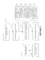
- FIG. 1illustrates a manufacturing system, including an Advanced Process Control (APC) framework, in accordance with one embodiment of the present invention
- FIG. 2depicts a block diagram of the manufacturing system of FIG. 1 employing a processing tool, in accordance with one embodiment of the present invention.
- FIG. 3illustrates a flow diagram of a method that may be implemented in the manufacturing system of FIG. 1 to associate process-related data with workpieces, in accordance with one embodiment of the present invention.
- FIG. 1a block diagram of a manufacturing system 100 for a semiconductor fabrication process is illustrated in accordance with one embodiment of the present invention.
- the inventionis described as it may be implemented in a semiconductor fabrication facility, the invention is not so limited and may be applied to other manufacturing environments.
- the techniques described hereinmay be applied to a variety of workpieces including, but not limited to, microprocessors, memory devices, digital signal processors, application specific integrated circuits (ASICs), or other similar devices.
- the techniquesmay also be applied to workpieces other than semiconductor devices.
- the system 100includes a plurality of processing tools 105 ( 1 - n ).
- the processing tools 105 ( 1 - n )are coupled to respective equipment interfaces (EI) 110 (shown as EI 110 ( 1 - n ) in FIG. 1 ).
- EIequipment interfaces
- Each of the equipment interfaces 110retrieves various operational data from its respective processing tool 105 , and communicates this data to an Advanced Process Control (APC) framework 120 to determine whether the processing tool 105 is experiencing faulty operation.
- APCAdvanced Process Control
- Each equipment interface 110may further receive control signals from the APC framework 120 that may be used to control the respective processing tool 105 .
- a control signal from the APC framework 120may be used to shut down the first processing tool 105 ( 1 ) if the operational data that was sent by the first equipment interface 110 ( 1 ) was deemed faulty by the APC framework 120 .
- operational datamay include data related to the processing of the workpieces, metrology data, and the like.
- Exemplary processing tools 105 ( 1 - n ) for a semiconductor device fabrication environmentinclude photolithography steppers, etch tools, deposition tools, polishing tools, rapid thermal processing tools, test-equipment tools, implantation tools, etc.
- the processing tool 105may be a multi-chambered processing tool.
- the processing tools 105 ( 1 - n )may be downstream to each other. That is, the second processing tool 105 ( 2 ) may be downstream to the first processing tool 105 ( 1 ), the third processing tool 105 ( 3 ), (not shown), may be downstream to the second processing tool 105 ( 2 ), and so forth.
- a workpiece that is processed by the first processing tool 105 ( 1 )may, for example, be provided to the second processing tool 105 ( 2 ), which may further process the workpiece before it is processed by the next processing tool 105 ( n ). This process may continue until the last processing tool 105 ( n ) has completed processing the workpiece.
- the processing tools 105 ( 1 - n ) of the system 100may perform various processing steps to create a packaged semiconductor device.
- the processing tools 105 ( 1 - n )may be used for manufacturing the raw semiconductor material, slicing the semiconductor crystal ingot into individual wafers, fabricating (e.g., etching, doping, ion implanting) the wafers, testing and packaging the completed semiconductor devices, and the like.
- the number of processing tools 105 ( 1 - n ) employed in the system 100may be implementation specific, and thus may vary from one embodiment to another depending on the particular processing steps desired.
- each processing tool 105performs selected processing steps in accordance with a recipe defined for the workpiece to be processed in the processing tool 105 .
- each recipemay define more than one processing step that can be performed by the processing tool 105 .
- the processing tool 105may process a plurality of workpieces at any given time under the control of a recipe, where, for example, the workpieces may be at varying process stages as they are processed by the processing tool 105 .
- the concept of accepting and then processing more than one workpiece at any given timeis sometimes referred to as “batch processing.”
- the “workpieces”are semiconductor wafers that are capable of being processed by the processing tools 105 ( 1 - n ).
- the processing tools 105may include one or more internal sensors (not shown) for measuring operational data, which may then be transmitted through the associated EI 110 of the processing tools 105 ( 1 - n ).
- the processing tools 105may also be coupled to respective external sensors 115 ( 1 - n ).
- the sensors 115 ( 1 - n )measure additional operational data that may or may not be ascertained by the associated processing tool 105 itself.
- the sensor 115may be used to determine a temperature range or other environmental or ambient data near or around the associated processing tool 105 .
- the sensor 115may be used to sense various other operational parameters associated with the processing tool 105 , and, thus, need not be limited to the aforementioned examples. It should be appreciated that, in one embodiment, some or all of the features of the sensors 115 ( 1 - n ) may be integrated within the processing tools 105 ( 1 - n ) themselves.
- the sensor 115may be embodied as a simple data acquisition program, such as a C++ standalone program acquiring data from a thermocouple wire. Alternatively, the sensor 115 may be embodied as a full-fledged LABVIEW application, acquiring data through multiple transducers (not shown). It will further be appreciated that the sensor 115 need not be used at all, and the APC framework 120 may rely upon the operational data forwarded from the processing tool 105 . If used, in one embodiment, the sensor 115 forwards the additional operational data to the APC framework 120 for analysis.
- the APC framework 120may be any one of a variety of arrangements that facilitates communications to and from the processing tools 105 ( 1 - n ).
- An exemplary information exchange and process control framework suitable for use in the manufacturing system 100is an Advanced Process Control (APC) framework, such as may be implemented using the Catalyst system offered by KLA-Tencor, Inc.
- the Catalyst systemuses Semiconductor Equipment and Materials International (SEMI) Computer Integrated Manufacturing (CIM) Framework compliant system technologies and is based on the Advanced Process Control (APC) Framework.
- SEMI E81-0699Provisional Specification for CIM Framework Domain Architecture
- APCSEMI E93-0999—Provisional Specification for CIM Framework Advanced Process Control Component
- the APC framework 120may include a control unit 121 that manages the communications to and from the APC framework 120 .
- the control unit 121may also control the overall operations of one or more of the processing tools 105 ( 1 - n ).
- Wafersmay take a variety of paths through the manufacturing system 100 as they are processed by various processing tools 105 ( 1 - n ) before arriving at the final product. Often, after the wafers are processed, several measurements of the final product may be taken to determine if the final product is compliant with the desired specification. These measurements are hereinafter referred to as “yield data.” Generally, if the yield data is outside the acceptable parameters, a fab technician may attempt to determine the source or cause of the process deviation in the manufacturing system 100 . However, the ability to identify the source or cause of the process deviation may depend in part on the amount and type of data that is collected as the wafers were processed.
- a limited amount and type of collected datamay inhibit or hamper the ability to properly identify the source of the problem that caused the undesirable results (e.g., process defects).
- a variety of types of operational dataare collected during the processing of the wafers. This variety of types of operation data enables a fab technician to more readily identify the potential source(s) of process deviations that may have ultimately affected the desired yield.
- the system 100includes a processor-based system 122 having a control unit 123 and a storage unit 124 .
- the processor-based system 122may include an interface to communicatively couple with the processing tool 105 via the APC framework 120 .
- the processor-based system 122receives the operational data associated with the processing tools 105 and processes the data to determine if a fault occurred in the manufacturing system 100 .
- the operational data that is associated with the processing tool 105may be received through the EI 110 , the sensor 115 , or any other desirable source.
- the illustrated components shown in the block diagram of the system 100 in FIG. 1are illustrative only, and that, in alternative embodiments, additional or fewer components may be utilized without deviating from the spirit or scope of the invention.
- the one or more processing tools 105may not have an external sensor 115 .
- various components, such as the equipment interface 110 of the system 100 of FIG. 1are shown as stand-alone components, in alternative embodiments, such components may be integrated into the processing tool 105 .
- the processor-based system 122may be integrated into the APC framework 120 .
- FIG. 2a block diagram of the manufacturing system 100 , including the processing tool 105 , the processor-based system 122 , and the APC framework 120 , is shown in accordance with one embodiment of the present invention.
- the processing tool 105is shown in FIG. 2 , although it should be appreciated that in other embodiments more than one processing tool 105 may be employed.
- the processing tool 105is shown having a controller 205 for managing the overall operation of the processing tool 105 .
- the processing tool 105 in the illustrated embodimentalso includes a plurality (three in this case) of processing chambers 220 ( 1 - 3 ). While three processing chambers 220 ( 1 - 3 ) are shown in FIG. 2 , it should be appreciated that in alternative embodiments, the processing tool 105 may have more or fewer processing chambers 220 ( 1 - 3 ).
- Each processing chamber 220 of the processing tool 105may perform one or more selected steps of the process as defined by the recipe. The particular type of process steps performed by the processing chambers 220 ( 1 - 3 ) depends in part on the type of processing tool 105 employed.
- a processing tool 105 that is an etching toolmay have an etching chamber, a stripping chamber, and a cool down chamber.
- a deposition toolfor example, may have a pre-depth etching chamber, a TI chemical vapor deposition chamber, and a TIN chemical vapor deposition chamber.
- the chambers 220 ( 1 - 3 ), in one embodiment,may have one or more chamber zones 225 associated therewith.
- the first chamber 220 ( 1 )has six chamber zones 225
- the second chamber 220 ( 2 )has two chamber zones 225
- the third chamber 220 ( 3 )has one chamber zone 225 .
- the number of zones 225 within the chamber 220may vary, depending on the particular implementation. It is not necessary that the incoming wafers be subjected to all of the zones 225 within a given chamber 220 .
- the number of zones 225 to which the incoming wafers may be exposed tomay depend, in part, on the process step called for by the recipe.
- An example of a processing tool 105 having one or more chambers 220includes a furnace tool, where the various “zones” may be temperature zones that are created as the wafer moves away from the heating element of the furnace tool.
- the processing tool 105 of FIG. 2may process a wafer, or, alternatively, a batch of wafers at a given time.
- each waferhas at least one identifier (hereinafter referred to as “wafer ID”) associated therewith.
- the processing tool 105may have an associated wafer ID reader 222 that is capable of identifying the wafers that enter the processing tool 105 .
- the wafer ID associated with each of the wafers that are processed by the processing tool 105is provided to the processor-based system 122 .
- a variety of informationis associated (or tagged) with the wafers that are processed by the processing tool 105 .
- This tagged informationmay be correlated to the processed wafers or a processed lot of wafers and used to improve the semiconductor process.
- the semiconductor processmay be improved, for example, by correlating the tagged information with the information collected from the processed wafers to identify one or more errors that may have caused deviations in the semiconductor process.
- FIG. 3a flow diagram of a method is illustrated, in accordance with one embodiment of the present invention.
- various types of process-related dataare collected while the wafers are processed by the processing tools 105 ( 1 - n ) in the manufacturing system 100 .
- the collected datain effect, “captures” at least a portion of the environment in which the wafers are processed.
- the processing tool 105receives (at 320 ) one or more wafers having an associated identifier (i.e., wafer ID).
- the processing tool 105may receive and process a batch of wafers. In one embodiment, the entire batch, as opposed to individual wafers, may have an associated ID.
- the processing tool 105processes (at 325 ) the one or more wafers.
- the processing tool 105associates (at 330 ) process-related data with one or more of the wafers as the wafers are processed by the processing tool 105 .
- process-related datamay be associated with (or tagged to) the wafers to preserve the characteristics of the environment in which the wafers are processed.
- associating (at 330 ) the process-related data with the wafersincludes associating (at 332 ) the type of the processing tool 105 (i.e., furnace, sink, implanter) that processes the wafers.
- associating (at 330 ) the process-related datamay include associating (at 334 ) data related to the various process steps that are performed by the processing tool 105 while processing the wafers during selected times.
- an implanting toolmay perform steps such as beam setup, beam tuning, and implanting.
- a rapid thermal anneal processing toolmay perform the steps of increasing a control value, such as voltage or temperature, to a preselected value, waiting a preselected interval before increasing the control value to a new preselected value, and detecting if the control value is within a desired range and letting the wafer cook or until the implanted impurities anneal.
- associating (at 330 ) the process-related datamay include associating (at 336 ) data identifying the chambers 220 ( 1 - 3 ) that process the wafers. Tagging chamber-level data to the wafers allows a fab technician to later determine, for example, the particular path the processed wafers traversed.
- associating (at 330 ) the process-related datamay include associating (at 338 ) data related to the chamber zones 225 of the processing tool 105 through which the wafers traverse as they are processed. It may be desirable to associate chamber zone-information with the wafers for subsequent die-level analysis of the processed wafers.
- Examples of various types of zonesmay include temperature zones or track zones. As mentioned, the type and number of zones may vary from one implementation to another, depending on the particular processing tool 105 . For instance, in a polishing tool the zones may be defined based on the mechanics of the polishing tool, such as whether the tool polishes sideways along the wafer, circular, and the like.
- associating (at 330 ) the process-related datamay include associating (at 340 ) data relating to the orientation of the wafer or wafers.
- This orientation datamay aid in reconstructing the relative position of the wafers inside the chamber zones 225 when the wafers were processed by the processing tool 105 .
- the orientation informationmay identify which portions of a wafer were exposed to which chamber zones 225 during processing.
- each waferhas a zero point of the wafer (i.e., the notch on the wafer) that defines its orientation.
- Associating wafer-orientation information with the wafersmay be useful for subsequent die-level analysis of the processed wafers.
- the controller 205 of the processing tool 105provides (at 345 ) the data associated (at 330 ) to the processor-based system 122 through the APC framework 120 for storage in the storage unit 124 .
- the stored datamay be readily accessed from the storage unit 124 of the processor-based system 122 for later use.
- a fab technicianmay acquire (at 350 ) yield data from the wafers that are processed by the processing tools 105 ( 1 - n ) of the manufacturing system 100 .
- the yield datamay be acquired (at 350 ) in any conventionally acceptable manner, and, in one embodiment, may be stored in the storage unit 124 of the processor-based system 122 .
- the process of acquiring the yield data (at 350 )may be an automated process.
- the processor-based system 122may execute one or more routines to obtain the yield data associated with the processed wafers.
- the data that was associated with the wafers during processing (at 330 )is correlated (at 360 ) with the yield data that is acquired (at 350 ) from the processed wafers.
- the processor-based system 122may be utilized to correlate (at 360 ) the collected data. Correlating the tagged data (at 360 ) with the yield data may be done for a variety of reasons, including identifying one or more sources that may have caused deviations in the semiconductor process or predicting yield impact. It may be possible to predict yield impact, for example, if an aberration in the processing of the wafer results in a particular, quantifiable yield.
- yield impactmay be predicted based on correlating the tagged data with the yield data. The ability to predict yield impact may allow fab technicians to refine the manufacturing process to obtain better results.
- control unitmay include a microprocessor, a microcontroller, a digital signal processor, a processor card (including one or more microprocessors or controllers), or other control or computing devices.
- the storage unit 124(see FIG. 1 ) referred to in this discussion may include one or more machine-readable storage media for storing data and instructions.
- the storage mediamay include different forms of memory including semiconductor memory devices such as dynamic or static random access memories (DRAMs or SRAMs), erasable and programmable read-only memories (EPROMs), electrically erasable and programmable read-only memories (EEPROMs) and flash memories; magnetic disks such as fixed, floppy, removable disks; other magnetic media including tape; and optical media such as compact disks (CDs) or digital video disks (DVDs).
- DRAMs or SRAMsdynamic or static random access memories
- EPROMserasable and programmable read-only memories
- EEPROMselectrically erasable and programmable read-only memories
- flash memoriessuch as fixed, floppy, removable disks
- CDscompact disks
- DVDsdigital video disks
Landscapes
- Engineering & Computer Science (AREA)
- General Engineering & Computer Science (AREA)
- Manufacturing & Machinery (AREA)
- Quality & Reliability (AREA)
- Physics & Mathematics (AREA)
- General Physics & Mathematics (AREA)
- Automation & Control Theory (AREA)
- General Factory Administration (AREA)
Abstract
Description
Claims (21)
Priority Applications (1)
| Application Number | Priority Date | Filing Date | Title |
|---|---|---|---|
| US10/185,468US8321048B1 (en) | 2002-06-28 | 2002-06-28 | Associating data with workpieces and correlating the data with yield data |
Applications Claiming Priority (1)
| Application Number | Priority Date | Filing Date | Title |
|---|---|---|---|
| US10/185,468US8321048B1 (en) | 2002-06-28 | 2002-06-28 | Associating data with workpieces and correlating the data with yield data |
Publications (1)
| Publication Number | Publication Date |
|---|---|
| US8321048B1true US8321048B1 (en) | 2012-11-27 |
Family
ID=47190955
Family Applications (1)
| Application Number | Title | Priority Date | Filing Date |
|---|---|---|---|
| US10/185,468Expired - Fee RelatedUS8321048B1 (en) | 2002-06-28 | 2002-06-28 | Associating data with workpieces and correlating the data with yield data |
Country Status (1)
| Country | Link |
|---|---|
| US (1) | US8321048B1 (en) |
Cited By (13)
| Publication number | Priority date | Publication date | Assignee | Title |
|---|---|---|---|---|
| US20060212740A1 (en)* | 2005-03-16 | 2006-09-21 | Jackson David B | Virtual Private Cluster |
| US9225663B2 (en) | 2005-03-16 | 2015-12-29 | Adaptive Computing Enterprises, Inc. | System and method providing a virtual private cluster |
| US10445146B2 (en) | 2006-03-16 | 2019-10-15 | Iii Holdings 12, Llc | System and method for managing a hybrid compute environment |
| US10608949B2 (en) | 2005-03-16 | 2020-03-31 | Iii Holdings 12, Llc | Simple integration of an on-demand compute environment |
| US11467883B2 (en) | 2004-03-13 | 2022-10-11 | Iii Holdings 12, Llc | Co-allocating a reservation spanning different compute resources types |
| US11496415B2 (en) | 2005-04-07 | 2022-11-08 | Iii Holdings 12, Llc | On-demand access to compute resources |
| US11494235B2 (en) | 2004-11-08 | 2022-11-08 | Iii Holdings 12, Llc | System and method of providing system jobs within a compute environment |
| US11522952B2 (en) | 2007-09-24 | 2022-12-06 | The Research Foundation For The State University Of New York | Automatic clustering for self-organizing grids |
| US11526304B2 (en) | 2009-10-30 | 2022-12-13 | Iii Holdings 2, Llc | Memcached server functionality in a cluster of data processing nodes |
| US11630704B2 (en) | 2004-08-20 | 2023-04-18 | Iii Holdings 12, Llc | System and method for a workload management and scheduling module to manage access to a compute environment according to local and non-local user identity information |
| US11652706B2 (en) | 2004-06-18 | 2023-05-16 | Iii Holdings 12, Llc | System and method for providing dynamic provisioning within a compute environment |
| US11720290B2 (en) | 2009-10-30 | 2023-08-08 | Iii Holdings 2, Llc | Memcached server functionality in a cluster of data processing nodes |
| US11960937B2 (en) | 2004-03-13 | 2024-04-16 | Iii Holdings 12, Llc | System and method for an optimizing reservation in time of compute resources based on prioritization function and reservation policy parameter |
Citations (23)
| Publication number | Priority date | Publication date | Assignee | Title |
|---|---|---|---|---|
| US5539752A (en)* | 1995-06-30 | 1996-07-23 | Advanced Micro Devices, Inc. | Method and system for automated analysis of semiconductor defect data |
| US5761065A (en)* | 1995-03-30 | 1998-06-02 | Advanced Micro Devices, Inc. | Arrangement and method for detecting sequential processing effects in manufacturing |
| US5856923A (en)* | 1997-03-24 | 1999-01-05 | Micron Technology, Inc. | Method for continuous, non lot-based integrated circuit manufacturing |
| US5923553A (en)* | 1995-12-21 | 1999-07-13 | Samsung Electronics Co., Ltd. | Method for controlling a semiconductor manufacturing process by failure analysis feedback |
| US5930138A (en)* | 1995-08-22 | 1999-07-27 | Advanced Micro Devices, Inc. | Arrangement and method for detecting sequential processing effects in manufacturing using predetermined sequences within runs |
| US5940300A (en)* | 1996-12-12 | 1999-08-17 | Mitsubishi Denki Kabushiki Kaisha | Method and apparatus for analyzing a fabrication line |
| US5993043A (en)* | 1996-11-29 | 1999-11-30 | Nec Corporation | Lithography processing apparatus for manufacturing semiconductor devices |
| US6180424B1 (en)* | 1997-12-05 | 2001-01-30 | Texas Instruments Incorporated | Method for improving wafer sleuth capability by adding wafer rotation tracking |
| US6298470B1 (en)* | 1999-04-15 | 2001-10-02 | Micron Technology, Inc. | Method for efficient manufacturing of integrated circuits |
| US6367040B1 (en)* | 1999-01-11 | 2002-04-02 | Siemens Aktiengesellschaft | System and method for determining yield impact for semiconductor devices |
| US6389323B1 (en)* | 1998-04-27 | 2002-05-14 | Taiwan Semiconductor Manufacturing Company | Method and system for yield loss analysis by yield management system |
| US20020069349A1 (en)* | 2000-12-04 | 2002-06-06 | Toprac Anthony J. | Method and apparatus for control of semiconductor processing for reducing effects of environmental effects |
| US6410351B1 (en)* | 2000-07-13 | 2002-06-25 | Advanced Micro Devices, Inc. | Method and apparatus for modeling thickness profiles and controlling subsequent etch process |
| US20020193902A1 (en)* | 2001-06-19 | 2002-12-19 | Applied Materials, Inc. | Integrating tool, module, and fab level control |
| US20030000922A1 (en)* | 2001-06-27 | 2003-01-02 | Ramkumar Subramanian | Using scatterometry to develop real time etch image |
| US20030014145A1 (en)* | 2001-07-16 | 2003-01-16 | Applied Materials, Inc. | Integration of fault detection with run-to-run control |
| US20030052084A1 (en)* | 2001-09-18 | 2003-03-20 | Tabery Cyrus E. | In-situ or ex-situ profile monitoring of phase openings on alternating phase shifting masks by scatterometry |
| US6662070B1 (en)* | 2000-03-08 | 2003-12-09 | Advanced Micro Devices, Inc. | Wafer rotation randomization in cluster tool processing |
| US20040005507A1 (en)* | 2000-05-04 | 2004-01-08 | Kla-Tencor, Inc. | Methods and systems for lithography process control |
| US6728591B1 (en)* | 2001-08-01 | 2004-04-27 | Advanced Micro Devices, Inc. | Method and apparatus for run-to-run control of trench profiles |
| US6766208B2 (en)* | 2001-09-24 | 2004-07-20 | Powerchip Semiconductor Corp. | Automatic production quality control method and system |
| US7082345B2 (en)* | 2001-06-19 | 2006-07-25 | Applied Materials, Inc. | Method, system and medium for process control for the matching of tools, chambers and/or other semiconductor-related entities |
| US20060246683A1 (en)* | 2002-06-11 | 2006-11-02 | Applied Materials, Inc. | Integrated equipment set for forming a low K dielectric interconnect on a substrate |
- 2002
- 2002-06-28USUS10/185,468patent/US8321048B1/ennot_activeExpired - Fee Related
Patent Citations (23)
| Publication number | Priority date | Publication date | Assignee | Title |
|---|---|---|---|---|
| US5761065A (en)* | 1995-03-30 | 1998-06-02 | Advanced Micro Devices, Inc. | Arrangement and method for detecting sequential processing effects in manufacturing |
| US5539752A (en)* | 1995-06-30 | 1996-07-23 | Advanced Micro Devices, Inc. | Method and system for automated analysis of semiconductor defect data |
| US5930138A (en)* | 1995-08-22 | 1999-07-27 | Advanced Micro Devices, Inc. | Arrangement and method for detecting sequential processing effects in manufacturing using predetermined sequences within runs |
| US5923553A (en)* | 1995-12-21 | 1999-07-13 | Samsung Electronics Co., Ltd. | Method for controlling a semiconductor manufacturing process by failure analysis feedback |
| US5993043A (en)* | 1996-11-29 | 1999-11-30 | Nec Corporation | Lithography processing apparatus for manufacturing semiconductor devices |
| US5940300A (en)* | 1996-12-12 | 1999-08-17 | Mitsubishi Denki Kabushiki Kaisha | Method and apparatus for analyzing a fabrication line |
| US5856923A (en)* | 1997-03-24 | 1999-01-05 | Micron Technology, Inc. | Method for continuous, non lot-based integrated circuit manufacturing |
| US6180424B1 (en)* | 1997-12-05 | 2001-01-30 | Texas Instruments Incorporated | Method for improving wafer sleuth capability by adding wafer rotation tracking |
| US6389323B1 (en)* | 1998-04-27 | 2002-05-14 | Taiwan Semiconductor Manufacturing Company | Method and system for yield loss analysis by yield management system |
| US6367040B1 (en)* | 1999-01-11 | 2002-04-02 | Siemens Aktiengesellschaft | System and method for determining yield impact for semiconductor devices |
| US6298470B1 (en)* | 1999-04-15 | 2001-10-02 | Micron Technology, Inc. | Method for efficient manufacturing of integrated circuits |
| US6662070B1 (en)* | 2000-03-08 | 2003-12-09 | Advanced Micro Devices, Inc. | Wafer rotation randomization in cluster tool processing |
| US20040005507A1 (en)* | 2000-05-04 | 2004-01-08 | Kla-Tencor, Inc. | Methods and systems for lithography process control |
| US6410351B1 (en)* | 2000-07-13 | 2002-06-25 | Advanced Micro Devices, Inc. | Method and apparatus for modeling thickness profiles and controlling subsequent etch process |
| US20020069349A1 (en)* | 2000-12-04 | 2002-06-06 | Toprac Anthony J. | Method and apparatus for control of semiconductor processing for reducing effects of environmental effects |
| US20020193902A1 (en)* | 2001-06-19 | 2002-12-19 | Applied Materials, Inc. | Integrating tool, module, and fab level control |
| US7082345B2 (en)* | 2001-06-19 | 2006-07-25 | Applied Materials, Inc. | Method, system and medium for process control for the matching of tools, chambers and/or other semiconductor-related entities |
| US20030000922A1 (en)* | 2001-06-27 | 2003-01-02 | Ramkumar Subramanian | Using scatterometry to develop real time etch image |
| US20030014145A1 (en)* | 2001-07-16 | 2003-01-16 | Applied Materials, Inc. | Integration of fault detection with run-to-run control |
| US6728591B1 (en)* | 2001-08-01 | 2004-04-27 | Advanced Micro Devices, Inc. | Method and apparatus for run-to-run control of trench profiles |
| US20030052084A1 (en)* | 2001-09-18 | 2003-03-20 | Tabery Cyrus E. | In-situ or ex-situ profile monitoring of phase openings on alternating phase shifting masks by scatterometry |
| US6766208B2 (en)* | 2001-09-24 | 2004-07-20 | Powerchip Semiconductor Corp. | Automatic production quality control method and system |
| US20060246683A1 (en)* | 2002-06-11 | 2006-11-02 | Applied Materials, Inc. | Integrated equipment set for forming a low K dielectric interconnect on a substrate |
Cited By (40)
| Publication number | Priority date | Publication date | Assignee | Title |
|---|---|---|---|---|
| US11467883B2 (en) | 2004-03-13 | 2022-10-11 | Iii Holdings 12, Llc | Co-allocating a reservation spanning different compute resources types |
| US12124878B2 (en) | 2004-03-13 | 2024-10-22 | Iii Holdings 12, Llc | System and method for scheduling resources within a compute environment using a scheduler process with reservation mask function |
| US11960937B2 (en) | 2004-03-13 | 2024-04-16 | Iii Holdings 12, Llc | System and method for an optimizing reservation in time of compute resources based on prioritization function and reservation policy parameter |
| US12009996B2 (en) | 2004-06-18 | 2024-06-11 | Iii Holdings 12, Llc | System and method for providing dynamic provisioning within a compute environment |
| US11652706B2 (en) | 2004-06-18 | 2023-05-16 | Iii Holdings 12, Llc | System and method for providing dynamic provisioning within a compute environment |
| US11630704B2 (en) | 2004-08-20 | 2023-04-18 | Iii Holdings 12, Llc | System and method for a workload management and scheduling module to manage access to a compute environment according to local and non-local user identity information |
| US11861404B2 (en) | 2004-11-08 | 2024-01-02 | Iii Holdings 12, Llc | System and method of providing system jobs within a compute environment |
| US11886915B2 (en) | 2004-11-08 | 2024-01-30 | Iii Holdings 12, Llc | System and method of providing system jobs within a compute environment |
| US12039370B2 (en) | 2004-11-08 | 2024-07-16 | Iii Holdings 12, Llc | System and method of providing system jobs within a compute environment |
| US12008405B2 (en) | 2004-11-08 | 2024-06-11 | Iii Holdings 12, Llc | System and method of providing system jobs within a compute environment |
| US11762694B2 (en) | 2004-11-08 | 2023-09-19 | Iii Holdings 12, Llc | System and method of providing system jobs within a compute environment |
| US11709709B2 (en) | 2004-11-08 | 2023-07-25 | Iii Holdings 12, Llc | System and method of providing system jobs within a compute environment |
| US11656907B2 (en) | 2004-11-08 | 2023-05-23 | Iii Holdings 12, Llc | System and method of providing system jobs within a compute environment |
| US11494235B2 (en) | 2004-11-08 | 2022-11-08 | Iii Holdings 12, Llc | System and method of providing system jobs within a compute environment |
| US11537434B2 (en) | 2004-11-08 | 2022-12-27 | Iii Holdings 12, Llc | System and method of providing system jobs within a compute environment |
| US11537435B2 (en) | 2004-11-08 | 2022-12-27 | Iii Holdings 12, Llc | System and method of providing system jobs within a compute environment |
| US11356385B2 (en) | 2005-03-16 | 2022-06-07 | Iii Holdings 12, Llc | On-demand compute environment |
| US8930536B2 (en)* | 2005-03-16 | 2015-01-06 | Adaptive Computing Enterprises, Inc. | Virtual private cluster |
| US12120040B2 (en) | 2005-03-16 | 2024-10-15 | Iii Holdings 12, Llc | On-demand compute environment |
| US9225663B2 (en) | 2005-03-16 | 2015-12-29 | Adaptive Computing Enterprises, Inc. | System and method providing a virtual private cluster |
| US10333862B2 (en) | 2005-03-16 | 2019-06-25 | Iii Holdings 12, Llc | Reserving resources in an on-demand compute environment |
| US9979672B2 (en) | 2005-03-16 | 2018-05-22 | Iii Holdings 12, Llc | System and method providing a virtual private cluster |
| US11134022B2 (en) | 2005-03-16 | 2021-09-28 | Iii Holdings 12, Llc | Simple integration of an on-demand compute environment |
| US9961013B2 (en) | 2005-03-16 | 2018-05-01 | Iii Holdings 12, Llc | Simple integration of on-demand compute environment |
| US11658916B2 (en) | 2005-03-16 | 2023-05-23 | Iii Holdings 12, Llc | Simple integration of an on-demand compute environment |
| US10608949B2 (en) | 2005-03-16 | 2020-03-31 | Iii Holdings 12, Llc | Simple integration of an on-demand compute environment |
| US20060212740A1 (en)* | 2005-03-16 | 2006-09-21 | Jackson David B | Virtual Private Cluster |
| US11765101B2 (en) | 2005-04-07 | 2023-09-19 | Iii Holdings 12, Llc | On-demand access to compute resources |
| US11831564B2 (en) | 2005-04-07 | 2023-11-28 | Iii Holdings 12, Llc | On-demand access to compute resources |
| US11496415B2 (en) | 2005-04-07 | 2022-11-08 | Iii Holdings 12, Llc | On-demand access to compute resources |
| US11522811B2 (en) | 2005-04-07 | 2022-12-06 | Iii Holdings 12, Llc | On-demand access to compute resources |
| US11533274B2 (en) | 2005-04-07 | 2022-12-20 | Iii Holdings 12, Llc | On-demand access to compute resources |
| US12155582B2 (en) | 2005-04-07 | 2024-11-26 | Iii Holdings 12, Llc | On-demand access to compute resources |
| US12160371B2 (en) | 2005-04-07 | 2024-12-03 | Iii Holdings 12, Llc | On-demand access to compute resources |
| US10445146B2 (en) | 2006-03-16 | 2019-10-15 | Iii Holdings 12, Llc | System and method for managing a hybrid compute environment |
| US11650857B2 (en) | 2006-03-16 | 2023-05-16 | Iii Holdings 12, Llc | System and method for managing a hybrid computer environment |
| US10977090B2 (en) | 2006-03-16 | 2021-04-13 | Iii Holdings 12, Llc | System and method for managing a hybrid compute environment |
| US11522952B2 (en) | 2007-09-24 | 2022-12-06 | The Research Foundation For The State University Of New York | Automatic clustering for self-organizing grids |
| US11526304B2 (en) | 2009-10-30 | 2022-12-13 | Iii Holdings 2, Llc | Memcached server functionality in a cluster of data processing nodes |
| US11720290B2 (en) | 2009-10-30 | 2023-08-08 | Iii Holdings 2, Llc | Memcached server functionality in a cluster of data processing nodes |
Similar Documents
| Publication | Publication Date | Title |
|---|---|---|
| KR101166209B1 (en) | Dynamic adaptive sampling rate for model prediction | |
| US8185230B2 (en) | Method and apparatus for predicting device electrical parameters during fabrication | |
| US7016750B2 (en) | Method, device, computer-readable storage medium and computer program element for monitoring of a manufacturing process | |
| US6647309B1 (en) | Method and apparatus for automated generation of test semiconductor wafers | |
| US6917849B1 (en) | Method and apparatus for predicting electrical parameters using measured and predicted fabrication parameters | |
| US6778873B1 (en) | Identifying a cause of a fault based on a process controller output | |
| US8321048B1 (en) | Associating data with workpieces and correlating the data with yield data | |
| KR101331249B1 (en) | Method and apparatus for manufacturing data indexing | |
| US6850811B1 (en) | Analyzing error signals based on fault detection | |
| US6804619B1 (en) | Process control based on tool health data | |
| US7051250B1 (en) | Routing workpieces based upon detecting a fault | |
| US20080275587A1 (en) | Fault detection on a multivariate sub-model | |
| US20060058979A1 (en) | Method and system for calibrating integrated metrology systems and stand-alone metrology systems that acquire wafer state data | |
| US7348187B2 (en) | Method, device, computer-readable storage medium and computer program element for the monitoring of a manufacturing process of a plurality of physical objects | |
| US6912433B1 (en) | Determining a next tool state based on fault detection information | |
| US7246290B1 (en) | Determining the health of a desired node in a multi-level system | |
| US8359494B2 (en) | Parallel fault detection | |
| US7130769B1 (en) | Method of dynamically designing a preventative maintenance schedule based upon sensor data, and system for accomplishing same | |
| US7337034B1 (en) | Method and apparatus for determining a root cause of a statistical process control failure | |
| US7236848B2 (en) | Data representation relating to a non-sampled workpiece | |
| US6988225B1 (en) | Verifying a fault detection result based on a process control state | |
| US7321993B1 (en) | Method and apparatus for fault detection classification of multiple tools based upon external data | |
| US6991945B1 (en) | Fault detection spanning multiple processes | |
| US6925347B1 (en) | Process control based on an estimated process result | |
| US7020535B1 (en) | Method and apparatus for providing excitation for a process controller |
Legal Events
| Date | Code | Title | Description |
|---|---|---|---|
| AS | Assignment | Owner name:ADVANCED MICRO DEVICES, INC., TEXAS Free format text:ASSIGNMENT OF ASSIGNORS INTEREST;ASSIGNORS:COSS, ELFIDO JR.;PETERSON, ANASTASIA O.;BODE, CHRISTOPHER A.;REEL/FRAME:013076/0231 Effective date:20020628 | |
| ZAAA | Notice of allowance and fees due | Free format text:ORIGINAL CODE: NOA | |
| ZAAB | Notice of allowance mailed | Free format text:ORIGINAL CODE: MN/=. | |
| STCF | Information on status: patent grant | Free format text:PATENTED CASE | |
| FPAY | Fee payment | Year of fee payment:4 | |
| MAFP | Maintenance fee payment | Free format text:PAYMENT OF MAINTENANCE FEE, 8TH YEAR, LARGE ENTITY (ORIGINAL EVENT CODE: M1552); ENTITY STATUS OF PATENT OWNER: LARGE ENTITY Year of fee payment:8 | |
| FEPP | Fee payment procedure | Free format text:MAINTENANCE FEE REMINDER MAILED (ORIGINAL EVENT CODE: REM.); ENTITY STATUS OF PATENT OWNER: LARGE ENTITY | |
| LAPS | Lapse for failure to pay maintenance fees | Free format text:PATENT EXPIRED FOR FAILURE TO PAY MAINTENANCE FEES (ORIGINAL EVENT CODE: EXP.); ENTITY STATUS OF PATENT OWNER: LARGE ENTITY | |
| STCH | Information on status: patent discontinuation | Free format text:PATENT EXPIRED DUE TO NONPAYMENT OF MAINTENANCE FEES UNDER 37 CFR 1.362 | |
| FP | Lapsed due to failure to pay maintenance fee | Effective date:20241127 |