US8319578B2 - Method and system for configurable differential or single-ended signaling in an integrated circuit - Google Patents
Method and system for configurable differential or single-ended signaling in an integrated circuitDownload PDFInfo
- Publication number
- US8319578B2 US8319578B2US13/306,555US201113306555AUS8319578B2US 8319578 B2US8319578 B2US 8319578B2US 201113306555 AUS201113306555 AUS 201113306555AUS 8319578 B2US8319578 B2US 8319578B2
- Authority
- US
- United States
- Prior art keywords
- balun
- signal
- integrated circuit
- unbalanced
- configurable
- Prior art date
- Legal status (The legal status is an assumption and is not a legal conclusion. Google has not performed a legal analysis and makes no representation as to the accuracy of the status listed.)
- Expired - Fee Related
Links
- 238000000034methodMethods0.000titleclaimsabstractdescription22
- 230000011664signalingEffects0.000titleabstractdescription12
- 230000005540biological transmissionEffects0.000claimsabstractdescription26
- 239000002184metalSubstances0.000claimsabstractdescription16
- 238000006243chemical reactionMethods0.000claimsabstractdescription15
- 239000003302ferromagnetic materialSubstances0.000claimsabstractdescription10
- 238000012545processingMethods0.000claimsdescription9
- 230000001939inductive effectEffects0.000claimsdescription7
- 230000008878couplingEffects0.000claimsdescription5
- 238000010168coupling processMethods0.000claimsdescription5
- 238000005859coupling reactionMethods0.000claimsdescription5
- 230000005291magnetic effectEffects0.000claimsdescription5
- 230000003321amplificationEffects0.000abstractdescription4
- 238000003199nucleic acid amplification methodMethods0.000abstractdescription4
- 238000010586diagramMethods0.000description8
- 238000004590computer programMethods0.000description4
- 239000003990capacitorSubstances0.000description3
- 230000001413cellular effectEffects0.000description3
- 230000003203everyday effectEffects0.000description3
- 238000010295mobile communicationMethods0.000description3
- 238000004804windingMethods0.000description3
- 239000004593EpoxySubstances0.000description2
- 238000005516engineering processMethods0.000description2
- 239000000463materialSubstances0.000description2
- 229910000679solderInorganic materials0.000description2
- 238000013459approachMethods0.000description1
- 238000013461designMethods0.000description1
- 239000004744fabricSubstances0.000description1
- 239000002902ferrimagnetic materialSubstances0.000description1
- 230000005294ferromagnetic effectEffects0.000description1
- 230000006870functionEffects0.000description1
- 238000010348incorporationMethods0.000description1
- 230000010365information processingEffects0.000description1
- 239000000696magnetic materialSubstances0.000description1
- 238000012986modificationMethods0.000description1
- 230000004048modificationEffects0.000description1
- 230000010287polarizationEffects0.000description1
- 230000008569processEffects0.000description1
Images

Classifications
- H—ELECTRICITY
- H03—ELECTRONIC CIRCUITRY
- H03H—IMPEDANCE NETWORKS, e.g. RESONANT CIRCUITS; RESONATORS
- H03H7/00—Multiple-port networks comprising only passive electrical elements as network components
- H03H7/42—Networks for transforming balanced signals into unbalanced signals and vice versa, e.g. baluns
- H03H7/422—Networks for transforming balanced signals into unbalanced signals and vice versa, e.g. baluns comprising distributed impedance elements together with lumped impedance elements
- H—ELECTRICITY
- H01—ELECTRIC ELEMENTS
- H01P—WAVEGUIDES; RESONATORS, LINES, OR OTHER DEVICES OF THE WAVEGUIDE TYPE
- H01P5/00—Coupling devices of the waveguide type
- H01P5/08—Coupling devices of the waveguide type for linking dissimilar lines or devices
- H01P5/10—Coupling devices of the waveguide type for linking dissimilar lines or devices for coupling balanced lines or devices with unbalanced lines or devices
- H—ELECTRICITY
- H03—ELECTRONIC CIRCUITRY
- H03H—IMPEDANCE NETWORKS, e.g. RESONANT CIRCUITS; RESONATORS
- H03H1/00—Constructional details of impedance networks whose electrical mode of operation is not specified or applicable to more than one type of network
- H03H2001/0021—Constructional details
- H03H2001/0085—Multilayer, e.g. LTCC, HTCC, green sheets
Definitions
- Certain embodiments of the inventionrelate to signal processing. More specifically, certain embodiments of the invention relate to a method and system for configurable differential or single-ended signaling in an integrated circuit.
- Mobile communicationshave changed the way people communicate and mobile phones have been transformed from a luxury item to an essential part of every day life.
- the use of mobile phonesis today dictated by social situations, rather than hampered by location or technology.
- voice connectionsfulfill the basic need to communicate, and mobile voice connections continue to filter even further into the fabric of every day life, the mobile Internet is the next step in the mobile communication revolution.
- the mobile Internetis poised to become a common source of everyday information, and easy, versatile mobile access to this data will be taken for granted.
- a system and/or method for configurable differential or single-ended signaling in an integrated circuitsubstantially as shown in and/or described in connection with at least one of the figures, as set forth more completely in the claims.
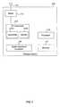
- FIG. 1is a block diagram illustrating an exemplary wireless device, in accordance with an embodiment of the invention.
- FIG. 2is a diagram of an exemplary balun transformer, in accordance with an embodiment of the invention.
- FIG. 3is a diagram illustrating an exemplary multi-layer balun, in accordance with an embodiment of the invention.
- FIG. 4is a diagram illustrating a cross-sectional view of a balun fabricated in an integrated circuit, in accordance with an embodiment of the invention.
- FIG. 5is a flow chart illustrating exemplary steps for converting between unbalanced and balanced signaling via an integrated balun, in accordance with an embodiment of the invention.
- baluncomprising one or more loops fabricated in a plurality of metal layers in an integrated circuit may enable conversion between unbalanced and balanced signals.
- balanced signal output by a power amplifiermay be converted to a balanced signal for transmission via an antenna.
- an unbalanced signal received by an antennamay be converted to a balanced signal for amplification by an amplifier with a balanced input.
- the loopsmay be fabricated in transmission line media such as microstrip and/or stripline.
- the loopsmay comprise ferromagnetic material which may be deposited on and/or within the IC. Signals converted via the balun may be in the 61 GHz-61.5 GHz ISM band.
- FIG. 1is a block diagram illustrating an exemplary wireless device, in accordance with an embodiment of the invention.
- a wireless device 120may comprise an RF transceiver 123 , a digital baseband processor 129 , a processor 425 , and a memory 127 .
- the transceiver 123may comprise a receiver 123 a and a transmitter 123 b .
- An antenna 121may be communicatively coupled to the RF transceiver 123 via the balun 112 .
- the wireless device 120may be operated in a system, such as the cellular network and/or digital video broadcast network, for example.
- the antenna 121may comprise one or more antenna elements which may be coupled and/or decoupled via one or more switching elements.
- the antenna 121may be configured based on factors comprising frequency, polarization, and/or gain.
- the antenna 121may be a phased array antenna.
- the directivity of the antennamay be controlled by adjusting the phase(s) of signals communicatively coupled to the antenna.
- the RF receiver 123 amay comprise suitable logic, circuitry, and/or code that may enable processing of received RF signals.
- the RF receiver 123 amay enable receiving RF signals in a plurality of frequency bands.
- the RF receiver 123 amay enable receiving signals in extremely high frequency (e.g., 60 GHz) bands.
- the receiver 123 amay be enabled to receive, filter, amplify, down-convert, and/or perform analog to digital conversion.
- the RF receiver 123 amay down convert a received RF signal.
- the RF receiver 123 amay perform direct down conversion of the received RF signal to a baseband or may convert the received RE signal to an intermediate frequency (IF).
- IFintermediate frequency
- the receiver 123 amay perform quadrature down-conversion where in-phase components and quadrature phase components may be processed in parallel.
- the receiver 123 amay be enabled to receive signals via the balun 112 , which may be configurable and provide a means for converting between differential and single ended signaling.
- the wireless device 120may comprise a plurality of the receivers 123 a and may thus support multiple frequency bands and or simultaneous reception of signals in the same frequency band.
- the digital baseband processor 129may comprise suitable logic, circuitry, and/or code that may enable processing and/or handling of baseband signals.
- the digital baseband processor 129may process or handle signals received from the RF receiver 123 a and/or signals to be transferred to the RF transmitter 123 b , when the RF transmitter 123 b is present, for transmission to the network.
- the digital baseband processor 129may also provide control and/or feedback information to the RF receiver 123 a and to the RF transmitter 123 b based on information from the processed signals.
- the baseband processor 129may provide one or more control signals for configuring the balun 112 via one or more switching elements.
- the digital baseband processor 129may communicate information and/or data from the processed signals to the processor 425 and/or to the memory 127 . Moreover, the digital baseband processor 129 may receive information from the processor 425 and/or to the memory 127 , which may be processed and transferred to the RF transmitter 123 b for transmission to the network.
- the RF transmitter 123 bmay comprise suitable logic, circuitry, and/or code that may enable processing of RF signals for transmission.
- the transmitter 123 bmay be enabled to transmit signals via the balun 112 , which may be configurable and provide a means for converting between single ended (unbalanced) and differential (balanced) signaling.
- the RF transmitter 123 bmay enable transmission of RF signals in a plurality of frequency bands.
- the RF transmitter 123 bmay enable transmitting signals in cellular frequency bands.
- Each frequency band supported by the RF transmitter 123 bmay have a corresponding front-end circuit for handling amplification and up conversion operations, for example.
- the RF transmitter 123 bmay be referred to as a multi-band transmitter when it supports more than one frequency band.
- the wireless device 120may comprise more than one RF transmitter 123 b , wherein each of the RF transmitters 123 b may be a single-band or a multi-band transmitter.
- the RF transmitter 123 bmay perform direct up conversion of the baseband signal to an RF signal. In some instances, the RF transmitter 123 b may enable digital-to-analog conversion of the baseband signal components received from the digital baseband processor 129 before up conversion. In other instances, the RF transmitter 123 b may receive baseband signal components in analog form.
- the processor 425may comprise suitable logic, circuitry, and/or code that may enable control and/or data processing operations for the wireless device 120 .
- the processor 425may be utilized to control at least a portion of the RF receiver 123 a , the RF transmitter 123 b , the digital baseband processor 129 , and/or the memory 127 .
- the processor 425may generate at least one signal for controlling operations within the wireless device 120 .
- the baseband processor 129may provide one or more control signals for configuring the balun 112 via one or more switching elements.
- the processor 425may also enable executing of applications that may be utilized by the wireless device 120 .
- the processor 425may execute applications that may enable displaying and/or interacting with content received via cellular transmission signals in the wireless device 120 .
- the memory 127may comprise suitable logic, circuitry, and/or code that may enable storage of data and/or other information utilized by the wireless device 120 .
- the memory 127may be utilized for storing processed data generated by the digital baseband processor 129 and/or the processor 425 .
- the memory 127may also be utilized to store information, such as configuration information, that may be utilized to control the operation of at least one block in the wireless device 120 .
- the memory 127may comprise information necessary to configure the balun 112 .
- the memorymay store control and/or configuration information for configuring the windings ratio of the transformer 112 via one or more switching elements.
- a wireless signalmay be received via the antenna 121 and conveyed to the transceiver 123 via the balun 112 fabricated in one or more metal layers of an integrated circuit in the wireless device 120 .
- the balunmay convert the unbalanced received signal from the antenna 121 to a balanced signal which may be processed by the transceiver.
- a signal transmitted by transceiver 123may be coupled to the antenna 121 via the balun 112 fabricated in one or more metal layers of an integrated circuit in the wireless device 120 .
- the balun 112may convert a balanced signal output by a power amplifier in the transceiver 123 into an unbalanced signal for transmission via the antenna 121 .
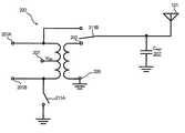
- FIG. 2is a diagram of an exemplary balun, in accordance with an embodiment of the invention.
- a balun 200there is shown a balun 200 , an antenna capacitor 207 , an antenna 121 , and switches 211 A and 211 B.
- the balun 200may comprise input terminals 201 A and 201 B, a DC bias tap 207 , and output terminals 203 and 205 .
- the antenna 121may be as described with respect to FIG. 1 .
- the antenna capacitor 207may enable improved impedance matching between the antenna 121 and the output impedance of the power amplifier in the transceiver 152 described with respect to FIG. 1 .
- the switches 211 B and 211 Bmay comprise microelectromechanical system (MEMS) switches or CMOS transistor switches on an integrated circuit, for example.
- MEMSmicroelectromechanical system
- an RF signal to be transmittedmay be communicated from a differential output power amplifier to the balanced inputs 201 A and 201 B of the balun 200 .
- the unbalanced output signalmay be communicated to the antenna 209 for transmission.
- the antenna capacitor 207may be configurable to adjust the impedance matching for different frequencies or different antennas in instances where more than one antenna may be utilized.
- an unbalanced signal suitable for transmissionmay be communicatively coupled to the terminal 201 a .
- the switch 211 Bmay be configured such that the input terminal 201 a may be coupled to the antenna 121 . Additionally the switch 211 a may communicatively couple the terminal 201 b to ground. In this manner, the balun 112 may be effectively bypassed.
- an unbalanced signal which may be unsuitable for transmission via the antenna 121may be communicatively coupled to the input terminal 201 a .
- the switch 211 amay communicatively couple the input terminal 201 b to ground and the switch 211 b may communicatively couple the output terminal 203 to the antenna 121 .
- the balun 112may provide impedance matching and/or otherwise condition the unbalanced signal for transmission via the antenna 121 .
- a balanced signalmay be communicatively coupled to the input terminals 201 . Accordingly, the switch 211 a may be open and the switch 211 b may communicatively couple the output terminal 203 to the antenna 121 . In this manner, the balanced signal may be converted to an unbalanced signal suitable for transmission via the antenna 121 .
- a signalmay be received via the antenna 121 and the switches 211 a and 211 b may be configured to impedance match the received signal to downstream circuitry, convert the received signal to a differential representation, or bypass the balun 112 .
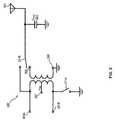
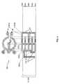
- FIG. 3is a diagram illustrating an exemplary multi-layer balun, in accordance with an embodiment of the invention.
- the balun 200comprising a plurality of conductive loops 304 a , 306 a , 304 b , 306 b , and 304 c arranged in a vertical stack and communicatively coupled via a plurality of vias 302 .
- the input terminals 201 A and 201 B, the DC bias tap 207 , and the output terminals 203 and 205may be as described with respect to FIG. 2 .
- a primary winding of the balun 200may comprise the loops 304 a , 304 b , and 304 c and a secondary winding may comprise the loops 306 a and 306 b .
- the integrated circuitmay comprise at least five metal layers, as described with respect to FIG. 4 .
- the integrated circuitmay be communicatively coupled to a multi-layer package.
- the integrated circuitmay be coupled to the package via a flip-chip bonding technique to reduce stray impedances.
- ferromagnetic materialmay be deposited in and/or on the integrated circuit 200 to improve the magnetic coupling of the loops in the balun 200 .
- the balun 200may be suited for processing signals in the 61-61.5 GHZ industrial, scientific, and medical (ISM) band.
- the inductive loops 304 and 306may be fabricated utilizing transmission line media such as stripline and/or microstrip.
- a differential RF signalmay be converted to a single ended signal by the balun 200 .
- the differential signalmay be communicatively coupled to the input terminals 201 a and 201 b via one or more metal layers and/or vias in the integrated circuit, as described with respect to FIG. 3 .
- FIG. 4is a diagram illustrating a cross-sectional view of a balun fabricated in an integrated circuit, in accordance with an embodiment of the invention.
- an integrated circuit 200there is shown an integrated circuit 200 , metal layers 402 , 404 , 406 , 408 and 410 , and interconnect 415 .
- the integrated circuit 200may, for example, comprise the transceiver 123 described with respect to FIG. 1 , or may also comprise any other integrated circuit within the wireless device 120 that may require conversion between single ended and differential signaling.
- the chip 401may be bump-bonded or flip-chip bonded to a multi-layer package via one or more solder balls. In this manner, wire bonds coupling the chip 200 to a multi-layer package may be eliminated, reducing and/or eliminating stray inductances due to wire bonds.
- the thermal conductance out of the chip 200may be greatly improved utilizing solder balls and thermal epoxy. Thermal epoxy may be electrically insulating but thermally conductive to allow for thermal energy to be conducted out of the chip 200 to the much larger thermal mass of a multilayer package.
- the loops 304 a , 306 a , 304 b , 306 b , and 304 cmay be fabricated in the metal layers 402 , 404 , 406 , 408 , and 410 , respectively.
- the metal layersmay comprise transmission line media such as strip-line and/or microstrip.
- the metal layers 402 , 404 , 406 , 408 , and 410may comprise ferromagnetic and/or ferrimagnetic materials utilized to improve magnetic coupling magnetic devices such as transformers, inductors, baluns, isolators, circulators, and gyrators.
- the magnetic materialsmay be deposited on the top, bottom and/or embedded within the integrated circuit 200 .
- the interconnects 415may comprise traces embedded in and/or deposited on the integrated circuit 200 that may be utilized as electrically conductive paths in the balun 200 and also to/from the balun 200 and other portions of the integrated circuit 200 .
- Various embodiments of the inventionmay comprise fewer and/or additional interconnects 415 , and thus the invention may not be limited to the number shown in FIG. 4 .
- the integrated circuit 200may comprise an RF front end, such as the RF transceiver 123 , described with respect to FIG. 1 , and may be utilized to transmit and receive RF signals. Additionally, the balun 200 may be configured, via one or more switches as described with respect to FIG. 2 , to perform differential to single ended conversion. For example, a balanced signal from a power amplifier may be communicatively coupled to the input terminals 201 a and 201 b via the metal layer 402 and/or one or more interconnects 415 . Accordingly, the balun 200 may convert the balanced signal into an unbalanced signal and may output the unbalanced signal to an antenna by way of the metal layers 404 and 408 and one or more interconnects 415 .
- a balanced signal from a power amplifiermay be communicatively coupled to the input terminals 201 a and 201 b via the metal layer 402 and/or one or more interconnects 415 . Accordingly, the balun 200 may convert the balanced signal into an unbalanced signal
- FIG. 5is a flow chart illustrating exemplary steps for converting between unbalanced and balanced signaling via an integrated balun, in accordance with an embodiment of the invention.
- the exemplary stepsmay advance to step 504 .
- the balun 200 of FIG. 2may be configured via one or more switching elements.
- the balun 20may be configured based on whether signals are to be received or transmitted via the antenna 121 .
- the balun 200may communicatively couple the antenna 121 to a unbalanced input of a low noise amplifier for reception and to a balanced output of a power amplifier for transmission.
- the exemplary stepsmay advance to step 506 .
- a signalmay be transmitted and/or received via the balun 200 and an associated antenna.
- a balunsuch as the balun 112 , comprising one or more loops fabricated in a plurality of metal layers in an integrated circuit, such as the IC 200 , may enable conversion between unbalanced and balanced signals.
- balanced signal output by a transmittersuch as the transmitter 123 a
- an antennasuch as the antenna 121
- an unbalanced signal received by the antenna 121may be converted to a balanced signal for amplification by a receiver, such as the receiver 123 b , with a balanced input.
- the loopsmay be fabricated in transmission line media such as microstrip and/or stripline.
- the loopsmay comprise ferromagnetic material which may be deposited on and/or within the IC.
- Signals converted via the balunmay be in the 61 GHz-61.5 GHz ISM band.
- Another embodiment of the inventionmay provide a machine-readable storage, having stored thereon, a computer program having at least one code section executable by a machine, thereby causing the machine to perform the steps as described herein for configurable differential or single-ended signaling in an integrated circuit.
- the present inventionmay be realized in hardware, software, or a combination of hardware and software.
- the present inventionmay be realized in a centralized fashion in at least one computer system, or in a distributed fashion where different elements are spread across several interconnected computer systems. Any kind of computer system or other apparatus adapted for carrying out the methods described herein is suited.
- a typical combination of hardware and softwaremay be a general-purpose computer system with a computer program that, when being loaded and executed, controls the computer system such that it carries out the methods described herein.
- the present inventionmay also be embedded in a computer program product, which comprises all the features enabling the implementation of the methods described herein, and which when loaded in a computer system is able to carry out these methods.
- Computer program in the present contextmeans any expression, in any language, code or notation, of a set of instructions intended to cause a system having an information processing capability to perform a particular function either directly or after either or both of the following: a) conversion to another language, code or notation; b) reproduction in a different material form.
Landscapes
- Transceivers (AREA)
- Semiconductor Integrated Circuits (AREA)
Abstract
Description
Claims (20)
Priority Applications (1)
| Application Number | Priority Date | Filing Date | Title |
|---|---|---|---|
| US13/306,555US8319578B2 (en) | 2008-03-27 | 2011-11-29 | Method and system for configurable differential or single-ended signaling in an integrated circuit |
Applications Claiming Priority (2)
| Application Number | Priority Date | Filing Date | Title |
|---|---|---|---|
| US12/056,525US8072287B2 (en) | 2008-03-27 | 2008-03-27 | Method and system for configurable differential or single-ended signaling in an integrated circuit |
| US13/306,555US8319578B2 (en) | 2008-03-27 | 2011-11-29 | Method and system for configurable differential or single-ended signaling in an integrated circuit |
Related Parent Applications (1)
| Application Number | Title | Priority Date | Filing Date |
|---|---|---|---|
| US12/056,525ContinuationUS8072287B2 (en) | 2008-03-27 | 2008-03-27 | Method and system for configurable differential or single-ended signaling in an integrated circuit |
Publications (2)
| Publication Number | Publication Date |
|---|---|
| US20120068782A1 US20120068782A1 (en) | 2012-03-22 |
| US8319578B2true US8319578B2 (en) | 2012-11-27 |
Family
ID=41116220
Family Applications (2)
| Application Number | Title | Priority Date | Filing Date |
|---|---|---|---|
| US12/056,525Expired - Fee RelatedUS8072287B2 (en) | 2008-03-27 | 2008-03-27 | Method and system for configurable differential or single-ended signaling in an integrated circuit |
| US13/306,555Expired - Fee RelatedUS8319578B2 (en) | 2008-03-27 | 2011-11-29 | Method and system for configurable differential or single-ended signaling in an integrated circuit |
Family Applications Before (1)
| Application Number | Title | Priority Date | Filing Date |
|---|---|---|---|
| US12/056,525Expired - Fee RelatedUS8072287B2 (en) | 2008-03-27 | 2008-03-27 | Method and system for configurable differential or single-ended signaling in an integrated circuit |
Country Status (1)
| Country | Link |
|---|---|
| US (2) | US8072287B2 (en) |
Cited By (2)
| Publication number | Priority date | Publication date | Assignee | Title |
|---|---|---|---|---|
| US10924139B2 (en)* | 2017-07-25 | 2021-02-16 | Guanddong Oppo Mobile Telecommunications Corp., Ltd. | Radio frequency circuit and electronic device |
| US12184311B2 (en) | 2021-03-25 | 2024-12-31 | Skyworks Solutions, Inc. | Antenna systems with both single-ended and differential signal feeds |
Families Citing this family (23)
| Publication number | Priority date | Publication date | Assignee | Title |
|---|---|---|---|---|
| US8583197B2 (en)* | 2007-12-12 | 2013-11-12 | Broadcom Corporation | Method and system for sharing antennas for high frequency and low frequency applications |
| US8270912B2 (en)* | 2007-12-12 | 2012-09-18 | Broadcom Corporation | Method and system for a transformer in an integrated circuit package |
| US7911388B2 (en)* | 2007-12-12 | 2011-03-22 | Broadcom Corporation | Method and system for configurable antenna in an integrated circuit package |
| US8144674B2 (en)* | 2008-03-27 | 2012-03-27 | Broadcom Corporation | Method and system for inter-PCB communications with wireline control |
| US7880677B2 (en)* | 2007-12-12 | 2011-02-01 | Broadcom Corporation | Method and system for a phased array antenna embedded in an integrated circuit package |
| US8494030B2 (en)* | 2008-06-19 | 2013-07-23 | Broadcom Corporation | Method and system for 60 GHz wireless clock distribution |
| US8106829B2 (en) | 2007-12-12 | 2012-01-31 | Broadcom Corporation | Method and system for an integrated antenna and antenna management |
| US8855093B2 (en)* | 2007-12-12 | 2014-10-07 | Broadcom Corporation | Method and system for chip-to-chip communications with wireline control |
| US8072287B2 (en)* | 2008-03-27 | 2011-12-06 | Broadcom Corporation | Method and system for configurable differential or single-ended signaling in an integrated circuit |
| US8086190B2 (en)* | 2008-03-27 | 2011-12-27 | Broadcom Corporation | Method and system for reconfigurable devices for multi-frequency coexistence |
| US8198714B2 (en)* | 2008-03-28 | 2012-06-12 | Broadcom Corporation | Method and system for configuring a transformer embedded in a multi-layer integrated circuit (IC) package |
| US8116676B2 (en)* | 2008-05-07 | 2012-02-14 | Broadcom Corporation | Method and system for inter IC communications utilizing a spatial multi-link repeater |
| US9264650B1 (en)* | 2009-05-16 | 2016-02-16 | Verint Video Solutions Inc. | Video encoder system |
| US8695884B2 (en) | 2011-08-25 | 2014-04-15 | Michael H. Baym | Systems, devices, admixtures, and methods including transponders for indication of food attributes |
| US9143366B2 (en) | 2012-09-07 | 2015-09-22 | The Aerospace Corporation | Galvanic isolation interface for high-speed data link for spacecraft electronics, and method of using same |
| US9431473B2 (en)* | 2012-11-21 | 2016-08-30 | Qualcomm Incorporated | Hybrid transformer structure on semiconductor devices |
| US10002700B2 (en)* | 2013-02-27 | 2018-06-19 | Qualcomm Incorporated | Vertical-coupling transformer with an air-gap structure |
| US9634645B2 (en) | 2013-03-14 | 2017-04-25 | Qualcomm Incorporated | Integration of a replica circuit and a transformer above a dielectric substrate |
| US9449753B2 (en) | 2013-08-30 | 2016-09-20 | Qualcomm Incorporated | Varying thickness inductor |
| US9906318B2 (en) | 2014-04-18 | 2018-02-27 | Qualcomm Incorporated | Frequency multiplexer |
| JP6769553B2 (en)* | 2017-06-30 | 2020-10-14 | 株式会社村田製作所 | Laminated balun |
| JP6769552B2 (en)* | 2017-06-30 | 2020-10-14 | 株式会社村田製作所 | Balun |
| US11876278B2 (en)* | 2021-03-29 | 2024-01-16 | Raytheon Company | Balun comprising stepped transitions between balance and unbalance connections, where the stepped transitions include ground rings of differing lengths connected by caged vias |
Citations (6)
| Publication number | Priority date | Publication date | Assignee | Title |
|---|---|---|---|---|
| US5015972A (en)* | 1989-08-17 | 1991-05-14 | Motorola, Inc. | Broadband RF transformer |
| US6603383B2 (en)* | 2000-12-22 | 2003-08-05 | Telefonaktiebolaget Lm Ericsson (Publ) | Multilayer balun transformer structure |
| US6982609B1 (en)* | 2002-05-15 | 2006-01-03 | Zeevo | System method and apparatus for a three-line balun with power amplifier bias |
| US7269391B2 (en)* | 2004-03-16 | 2007-09-11 | Broadcom Corporation | Tunable transceiver front end |
| US7859359B2 (en)* | 2008-02-25 | 2010-12-28 | Broadcom Corporation | Method and system for a balun embedded in an integrated circuit package |
| US8072287B2 (en)* | 2008-03-27 | 2011-12-06 | Broadcom Corporation | Method and system for configurable differential or single-ended signaling in an integrated circuit |
Family Cites Families (22)
| Publication number | Priority date | Publication date | Assignee | Title |
|---|---|---|---|---|
| JPH0319358A (en) | 1989-06-16 | 1991-01-28 | Matsushita Electron Corp | Semiconductor integrated circuit |
| US5003622A (en)* | 1989-09-26 | 1991-03-26 | Astec International Limited | Printed circuit transformer |
| US5861853A (en)* | 1997-05-07 | 1999-01-19 | Motorola, Inc. | Current balanced balun network with selectable port impedances |
| US6801114B2 (en)* | 2002-01-23 | 2004-10-05 | Broadcom Corp. | Integrated radio having on-chip transformer balun |
| US6809581B2 (en)* | 2002-04-23 | 2004-10-26 | Broadcom Corp. | Integrated circuit low noise amplifier and applications thereof |
| US7399661B2 (en)* | 2002-05-01 | 2008-07-15 | Amkor Technology, Inc. | Method for making an integrated circuit substrate having embedded back-side access conductors and vias |
| US7283793B1 (en)* | 2002-05-15 | 2007-10-16 | Broadcom Corporation | Package filter and combiner network |
| US7138884B2 (en)* | 2002-08-19 | 2006-11-21 | Dsp Group Inc. | Circuit package integrating passive radio frequency structure |
| US7141883B2 (en)* | 2002-10-15 | 2006-11-28 | Silicon Laboratories Inc. | Integrated circuit package configuration incorporating shielded circuit element structure |
| US7151506B2 (en)* | 2003-04-11 | 2006-12-19 | Qortek, Inc. | Electromagnetic energy coupling mechanism with matrix architecture control |
| US7180381B2 (en)* | 2004-04-21 | 2007-02-20 | Synergy Microwave Corporation | Wideband voltage controlled oscillator employing evanescent mode coupled-resonators |
| US7081800B2 (en)* | 2004-06-30 | 2006-07-25 | Intel Corporation | Package integrated one-quarter wavelength and three-quarter wavelength balun |
| US7129784B2 (en)* | 2004-10-28 | 2006-10-31 | Broadcom Corporation | Multilevel power amplifier architecture using multi-tap transformer |
| US7342499B2 (en)* | 2006-01-26 | 2008-03-11 | Printronix, Inc. | Multi-band RFID encoder |
| US7620175B2 (en)* | 2006-07-24 | 2009-11-17 | Motorola, Inc. | Handset device with audio porting |
| US7675465B2 (en)* | 2007-05-22 | 2010-03-09 | Sibeam, Inc. | Surface mountable integrated circuit packaging scheme |
| US8270912B2 (en)* | 2007-12-12 | 2012-09-18 | Broadcom Corporation | Method and system for a transformer in an integrated circuit package |
| US20090153260A1 (en)* | 2007-12-12 | 2009-06-18 | Ahmadreza Rofougaran | Method and system for a configurable transformer integrated on chip |
| US7911388B2 (en)* | 2007-12-12 | 2011-03-22 | Broadcom Corporation | Method and system for configurable antenna in an integrated circuit package |
| US7880677B2 (en)* | 2007-12-12 | 2011-02-01 | Broadcom Corporation | Method and system for a phased array antenna embedded in an integrated circuit package |
| US8106829B2 (en)* | 2007-12-12 | 2012-01-31 | Broadcom Corporation | Method and system for an integrated antenna and antenna management |
| US20090243741A1 (en)* | 2008-03-27 | 2009-10-01 | Ahmadreza Rofougaran | Method and system for processing signals via an oscillator load embedded in an integrated circuit (ic) package |
- 2008
- 2008-03-27USUS12/056,525patent/US8072287B2/ennot_activeExpired - Fee Related
- 2011
- 2011-11-29USUS13/306,555patent/US8319578B2/ennot_activeExpired - Fee Related
Patent Citations (6)
| Publication number | Priority date | Publication date | Assignee | Title |
|---|---|---|---|---|
| US5015972A (en)* | 1989-08-17 | 1991-05-14 | Motorola, Inc. | Broadband RF transformer |
| US6603383B2 (en)* | 2000-12-22 | 2003-08-05 | Telefonaktiebolaget Lm Ericsson (Publ) | Multilayer balun transformer structure |
| US6982609B1 (en)* | 2002-05-15 | 2006-01-03 | Zeevo | System method and apparatus for a three-line balun with power amplifier bias |
| US7269391B2 (en)* | 2004-03-16 | 2007-09-11 | Broadcom Corporation | Tunable transceiver front end |
| US7859359B2 (en)* | 2008-02-25 | 2010-12-28 | Broadcom Corporation | Method and system for a balun embedded in an integrated circuit package |
| US8072287B2 (en)* | 2008-03-27 | 2011-12-06 | Broadcom Corporation | Method and system for configurable differential or single-ended signaling in an integrated circuit |
Cited By (2)
| Publication number | Priority date | Publication date | Assignee | Title |
|---|---|---|---|---|
| US10924139B2 (en)* | 2017-07-25 | 2021-02-16 | Guanddong Oppo Mobile Telecommunications Corp., Ltd. | Radio frequency circuit and electronic device |
| US12184311B2 (en) | 2021-03-25 | 2024-12-31 | Skyworks Solutions, Inc. | Antenna systems with both single-ended and differential signal feeds |
Also Published As
| Publication number | Publication date |
|---|---|
| US20120068782A1 (en) | 2012-03-22 |
| US20090243749A1 (en) | 2009-10-01 |
| US8072287B2 (en) | 2011-12-06 |
Similar Documents
| Publication | Publication Date | Title |
|---|---|---|
| US8319578B2 (en) | Method and system for configurable differential or single-ended signaling in an integrated circuit | |
| US8855581B2 (en) | Integrated circuit package with transformer | |
| US8912639B2 (en) | IC package with embedded transformer | |
| US8106829B2 (en) | Method and system for an integrated antenna and antenna management | |
| US20090153260A1 (en) | Method and system for a configurable transformer integrated on chip | |
| US8174451B2 (en) | Method and system for configurable antenna in an integrated circuit package | |
| US8199060B2 (en) | Method and system for a phased array antenna embedded in an integrated circuit package | |
| US7944322B2 (en) | Method and system for flip chip configurable RF front end with an off-chip balun | |
| US7859359B2 (en) | Method and system for a balun embedded in an integrated circuit package | |
| US8659366B2 (en) | MEMS switches in an integrated circuit package | |
| US8768269B2 (en) | MEMS and switched capacitors configured for increased resolution switching | |
| TW202324609A (en) | Radio-frequency switch having redistribution layer inductance | |
| HK1138121B (en) | A method and system for transformer in ic package |
Legal Events
| Date | Code | Title | Description |
|---|---|---|---|
| STCF | Information on status: patent grant | Free format text:PATENTED CASE | |
| AS | Assignment | Owner name:BANK OF AMERICA, N.A., AS COLLATERAL AGENT, NORTH CAROLINA Free format text:PATENT SECURITY AGREEMENT;ASSIGNOR:BROADCOM CORPORATION;REEL/FRAME:037806/0001 Effective date:20160201 Owner name:BANK OF AMERICA, N.A., AS COLLATERAL AGENT, NORTH Free format text:PATENT SECURITY AGREEMENT;ASSIGNOR:BROADCOM CORPORATION;REEL/FRAME:037806/0001 Effective date:20160201 | |
| FPAY | Fee payment | Year of fee payment:4 | |
| AS | Assignment | Owner name:AVAGO TECHNOLOGIES GENERAL IP (SINGAPORE) PTE. LTD., SINGAPORE Free format text:ASSIGNMENT OF ASSIGNORS INTEREST;ASSIGNOR:BROADCOM CORPORATION;REEL/FRAME:041706/0001 Effective date:20170120 Owner name:AVAGO TECHNOLOGIES GENERAL IP (SINGAPORE) PTE. LTD Free format text:ASSIGNMENT OF ASSIGNORS INTEREST;ASSIGNOR:BROADCOM CORPORATION;REEL/FRAME:041706/0001 Effective date:20170120 | |
| AS | Assignment | Owner name:BROADCOM CORPORATION, CALIFORNIA Free format text:TERMINATION AND RELEASE OF SECURITY INTEREST IN PATENTS;ASSIGNOR:BANK OF AMERICA, N.A., AS COLLATERAL AGENT;REEL/FRAME:041712/0001 Effective date:20170119 | |
| AS | Assignment | Owner name:AVAGO TECHNOLOGIES INTERNATIONAL SALES PTE. LIMITE Free format text:MERGER;ASSIGNOR:AVAGO TECHNOLOGIES GENERAL IP (SINGAPORE) PTE. LTD.;REEL/FRAME:047230/0133 Effective date:20180509 | |
| AS | Assignment | Owner name:AVAGO TECHNOLOGIES INTERNATIONAL SALES PTE. LIMITE Free format text:CORRECTIVE ASSIGNMENT TO CORRECT THE EFFECTIVE DATE OF MERGER TO 09/05/2018 PREVIOUSLY RECORDED AT REEL: 047230 FRAME: 0133. ASSIGNOR(S) HEREBY CONFIRMS THE MERGER;ASSIGNOR:AVAGO TECHNOLOGIES GENERAL IP (SINGAPORE) PTE. LTD.;REEL/FRAME:047630/0456 Effective date:20180905 | |
| FEPP | Fee payment procedure | Free format text:MAINTENANCE FEE REMINDER MAILED (ORIGINAL EVENT CODE: REM.); ENTITY STATUS OF PATENT OWNER: LARGE ENTITY | |
| LAPS | Lapse for failure to pay maintenance fees | Free format text:PATENT EXPIRED FOR FAILURE TO PAY MAINTENANCE FEES (ORIGINAL EVENT CODE: EXP.); ENTITY STATUS OF PATENT OWNER: LARGE ENTITY | |
| STCH | Information on status: patent discontinuation | Free format text:PATENT EXPIRED DUE TO NONPAYMENT OF MAINTENANCE FEES UNDER 37 CFR 1.362 | |
| FP | Lapsed due to failure to pay maintenance fee | Effective date:20201127 |