US8319318B2 - Forming metal filled die back-side film for electromagnetic interference shielding with coreless packages - Google Patents
Forming metal filled die back-side film for electromagnetic interference shielding with coreless packagesDownload PDFInfo
- Publication number
- US8319318B2 US8319318B2US12/755,201US75520110AUS8319318B2US 8319318 B2US8319318 B2US 8319318B2US 75520110 AUS75520110 AUS 75520110AUS 8319318 B2US8319318 B2US 8319318B2
- Authority
- US
- United States
- Prior art keywords
- die
- dbf
- coreless
- coreless substrate
- top surface
- Prior art date
- Legal status (The legal status is an assumption and is not a legal conclusion. Google has not performed a legal analysis and makes no representation as to the accuracy of the status listed.)
- Active, expires
Links
Images


Classifications
- H—ELECTRICITY
- H01—ELECTRIC ELEMENTS
- H01L—SEMICONDUCTOR DEVICES NOT COVERED BY CLASS H10
- H01L23/00—Details of semiconductor or other solid state devices
- H01L23/58—Structural electrical arrangements for semiconductor devices not otherwise provided for, e.g. in combination with batteries
- H01L23/585—Structural electrical arrangements for semiconductor devices not otherwise provided for, e.g. in combination with batteries comprising conductive layers or plates or strips or rods or rings
- H—ELECTRICITY
- H01—ELECTRIC ELEMENTS
- H01L—SEMICONDUCTOR DEVICES NOT COVERED BY CLASS H10
- H01L21/00—Processes or apparatus adapted for the manufacture or treatment of semiconductor or solid state devices or of parts thereof
- H01L21/02—Manufacture or treatment of semiconductor devices or of parts thereof
- H01L21/04—Manufacture or treatment of semiconductor devices or of parts thereof the devices having potential barriers, e.g. a PN junction, depletion layer or carrier concentration layer
- H01L21/50—Assembly of semiconductor devices using processes or apparatus not provided for in a single one of the groups H01L21/18 - H01L21/326 or H10D48/04 - H10D48/07 e.g. sealing of a cap to a base of a container
- H01L21/56—Encapsulations, e.g. encapsulation layers, coatings
- H01L21/568—Temporary substrate used as encapsulation process aid
- H—ELECTRICITY
- H01—ELECTRIC ELEMENTS
- H01L—SEMICONDUCTOR DEVICES NOT COVERED BY CLASS H10
- H01L21/00—Processes or apparatus adapted for the manufacture or treatment of semiconductor or solid state devices or of parts thereof
- H01L21/67—Apparatus specially adapted for handling semiconductor or electric solid state devices during manufacture or treatment thereof; Apparatus specially adapted for handling wafers during manufacture or treatment of semiconductor or electric solid state devices or components ; Apparatus not specifically provided for elsewhere
- H01L21/683—Apparatus specially adapted for handling semiconductor or electric solid state devices during manufacture or treatment thereof; Apparatus specially adapted for handling wafers during manufacture or treatment of semiconductor or electric solid state devices or components ; Apparatus not specifically provided for elsewhere for supporting or gripping
- H01L21/6835—Apparatus specially adapted for handling semiconductor or electric solid state devices during manufacture or treatment thereof; Apparatus specially adapted for handling wafers during manufacture or treatment of semiconductor or electric solid state devices or components ; Apparatus not specifically provided for elsewhere for supporting or gripping using temporarily an auxiliary support
- H—ELECTRICITY
- H01—ELECTRIC ELEMENTS
- H01L—SEMICONDUCTOR DEVICES NOT COVERED BY CLASS H10
- H01L23/00—Details of semiconductor or other solid state devices
- H01L23/28—Encapsulations, e.g. encapsulating layers, coatings, e.g. for protection
- H01L23/31—Encapsulations, e.g. encapsulating layers, coatings, e.g. for protection characterised by the arrangement or shape
- H01L23/3107—Encapsulations, e.g. encapsulating layers, coatings, e.g. for protection characterised by the arrangement or shape the device being completely enclosed
- H01L23/3121—Encapsulations, e.g. encapsulating layers, coatings, e.g. for protection characterised by the arrangement or shape the device being completely enclosed a substrate forming part of the encapsulation
- H01L23/3128—Encapsulations, e.g. encapsulating layers, coatings, e.g. for protection characterised by the arrangement or shape the device being completely enclosed a substrate forming part of the encapsulation the substrate having spherical bumps for external connection
- H—ELECTRICITY
- H01—ELECTRIC ELEMENTS
- H01L—SEMICONDUCTOR DEVICES NOT COVERED BY CLASS H10
- H01L23/00—Details of semiconductor or other solid state devices
- H01L23/48—Arrangements for conducting electric current to or from the solid state body in operation, e.g. leads, terminal arrangements ; Selection of materials therefor
- H—ELECTRICITY
- H01—ELECTRIC ELEMENTS
- H01L—SEMICONDUCTOR DEVICES NOT COVERED BY CLASS H10
- H01L23/00—Details of semiconductor or other solid state devices
- H01L23/552—Protection against radiation, e.g. light or electromagnetic waves
- H—ELECTRICITY
- H01—ELECTRIC ELEMENTS
- H01L—SEMICONDUCTOR DEVICES NOT COVERED BY CLASS H10
- H01L2221/00—Processes or apparatus adapted for the manufacture or treatment of semiconductor or solid state devices or of parts thereof covered by H01L21/00
- H01L2221/67—Apparatus for handling semiconductor or electric solid state devices during manufacture or treatment thereof; Apparatus for handling wafers during manufacture or treatment of semiconductor or electric solid state devices or components; Apparatus not specifically provided for elsewhere
- H01L2221/683—Apparatus for handling semiconductor or electric solid state devices during manufacture or treatment thereof; Apparatus for handling wafers during manufacture or treatment of semiconductor or electric solid state devices or components; Apparatus not specifically provided for elsewhere for supporting or gripping
- H01L2221/68304—Apparatus for handling semiconductor or electric solid state devices during manufacture or treatment thereof; Apparatus for handling wafers during manufacture or treatment of semiconductor or electric solid state devices or components; Apparatus not specifically provided for elsewhere for supporting or gripping using temporarily an auxiliary support
- H01L2221/68345—Apparatus for handling semiconductor or electric solid state devices during manufacture or treatment thereof; Apparatus for handling wafers during manufacture or treatment of semiconductor or electric solid state devices or components; Apparatus not specifically provided for elsewhere for supporting or gripping using temporarily an auxiliary support used as a support during the manufacture of self supporting substrates
- H—ELECTRICITY
- H01—ELECTRIC ELEMENTS
- H01L—SEMICONDUCTOR DEVICES NOT COVERED BY CLASS H10
- H01L2224/00—Indexing scheme for arrangements for connecting or disconnecting semiconductor or solid-state bodies and methods related thereto as covered by H01L24/00
- H01L2224/01—Means for bonding being attached to, or being formed on, the surface to be connected, e.g. chip-to-package, die-attach, "first-level" interconnects; Manufacturing methods related thereto
- H01L2224/10—Bump connectors; Manufacturing methods related thereto
- H01L2224/12—Structure, shape, material or disposition of the bump connectors prior to the connecting process
- H01L2224/12105—Bump connectors formed on an encapsulation of the semiconductor or solid-state body, e.g. bumps on chip-scale packages
- H—ELECTRICITY
- H01—ELECTRIC ELEMENTS
- H01L—SEMICONDUCTOR DEVICES NOT COVERED BY CLASS H10
- H01L2224/00—Indexing scheme for arrangements for connecting or disconnecting semiconductor or solid-state bodies and methods related thereto as covered by H01L24/00
- H01L2224/01—Means for bonding being attached to, or being formed on, the surface to be connected, e.g. chip-to-package, die-attach, "first-level" interconnects; Manufacturing methods related thereto
- H01L2224/10—Bump connectors; Manufacturing methods related thereto
- H01L2224/12—Structure, shape, material or disposition of the bump connectors prior to the connecting process
- H01L2224/13—Structure, shape, material or disposition of the bump connectors prior to the connecting process of an individual bump connector
- H01L2224/13001—Core members of the bump connector
- H01L2224/1302—Disposition
- H01L2224/13021—Disposition the bump connector being disposed in a recess of the surface
- H—ELECTRICITY
- H01—ELECTRIC ELEMENTS
- H01L—SEMICONDUCTOR DEVICES NOT COVERED BY CLASS H10
- H01L2224/00—Indexing scheme for arrangements for connecting or disconnecting semiconductor or solid-state bodies and methods related thereto as covered by H01L24/00
- H01L2224/01—Means for bonding being attached to, or being formed on, the surface to be connected, e.g. chip-to-package, die-attach, "first-level" interconnects; Manufacturing methods related thereto
- H01L2224/18—High density interconnect [HDI] connectors; Manufacturing methods related thereto
- H01L2224/20—Structure, shape, material or disposition of high density interconnect preforms
- H01L2224/21—Structure, shape, material or disposition of high density interconnect preforms of an individual HDI interconnect
- H01L2224/2101—Structure
- H—ELECTRICITY
- H01—ELECTRIC ELEMENTS
- H01L—SEMICONDUCTOR DEVICES NOT COVERED BY CLASS H10
- H01L2224/00—Indexing scheme for arrangements for connecting or disconnecting semiconductor or solid-state bodies and methods related thereto as covered by H01L24/00
- H01L2224/01—Means for bonding being attached to, or being formed on, the surface to be connected, e.g. chip-to-package, die-attach, "first-level" interconnects; Manufacturing methods related thereto
- H01L2224/18—High density interconnect [HDI] connectors; Manufacturing methods related thereto
- H01L2224/20—Structure, shape, material or disposition of high density interconnect preforms
- H01L2224/22—Structure, shape, material or disposition of high density interconnect preforms of a plurality of HDI interconnects
- H01L2224/221—Disposition
- H—ELECTRICITY
- H01—ELECTRIC ELEMENTS
- H01L—SEMICONDUCTOR DEVICES NOT COVERED BY CLASS H10
- H01L24/00—Arrangements for connecting or disconnecting semiconductor or solid-state bodies; Methods or apparatus related thereto
- H01L24/01—Means for bonding being attached to, or being formed on, the surface to be connected, e.g. chip-to-package, die-attach, "first-level" interconnects; Manufacturing methods related thereto
- H01L24/18—High density interconnect [HDI] connectors; Manufacturing methods related thereto
- H01L24/19—Manufacturing methods of high density interconnect preforms
- H—ELECTRICITY
- H01—ELECTRIC ELEMENTS
- H01L—SEMICONDUCTOR DEVICES NOT COVERED BY CLASS H10
- H01L24/00—Arrangements for connecting or disconnecting semiconductor or solid-state bodies; Methods or apparatus related thereto
- H01L24/01—Means for bonding being attached to, or being formed on, the surface to be connected, e.g. chip-to-package, die-attach, "first-level" interconnects; Manufacturing methods related thereto
- H01L24/18—High density interconnect [HDI] connectors; Manufacturing methods related thereto
- H01L24/20—Structure, shape, material or disposition of high density interconnect preforms
- H—ELECTRICITY
- H01—ELECTRIC ELEMENTS
- H01L—SEMICONDUCTOR DEVICES NOT COVERED BY CLASS H10
- H01L2924/00—Indexing scheme for arrangements or methods for connecting or disconnecting semiconductor or solid-state bodies as covered by H01L24/00
- H01L2924/01—Chemical elements
- H01L2924/01006—Carbon [C]
- H—ELECTRICITY
- H01—ELECTRIC ELEMENTS
- H01L—SEMICONDUCTOR DEVICES NOT COVERED BY CLASS H10
- H01L2924/00—Indexing scheme for arrangements or methods for connecting or disconnecting semiconductor or solid-state bodies as covered by H01L24/00
- H01L2924/01—Chemical elements
- H01L2924/01029—Copper [Cu]
- H—ELECTRICITY
- H01—ELECTRIC ELEMENTS
- H01L—SEMICONDUCTOR DEVICES NOT COVERED BY CLASS H10
- H01L2924/00—Indexing scheme for arrangements or methods for connecting or disconnecting semiconductor or solid-state bodies as covered by H01L24/00
- H01L2924/01—Chemical elements
- H01L2924/01033—Arsenic [As]
- H—ELECTRICITY
- H01—ELECTRIC ELEMENTS
- H01L—SEMICONDUCTOR DEVICES NOT COVERED BY CLASS H10
- H01L2924/00—Indexing scheme for arrangements or methods for connecting or disconnecting semiconductor or solid-state bodies as covered by H01L24/00
- H01L2924/01—Chemical elements
- H01L2924/01047—Silver [Ag]
- H—ELECTRICITY
- H01—ELECTRIC ELEMENTS
- H01L—SEMICONDUCTOR DEVICES NOT COVERED BY CLASS H10
- H01L2924/00—Indexing scheme for arrangements or methods for connecting or disconnecting semiconductor or solid-state bodies as covered by H01L24/00
- H01L2924/01—Chemical elements
- H01L2924/01057—Lanthanum [La]
- H—ELECTRICITY
- H01—ELECTRIC ELEMENTS
- H01L—SEMICONDUCTOR DEVICES NOT COVERED BY CLASS H10
- H01L2924/00—Indexing scheme for arrangements or methods for connecting or disconnecting semiconductor or solid-state bodies as covered by H01L24/00
- H01L2924/10—Details of semiconductor or other solid state devices to be connected
- H01L2924/11—Device type
- H01L2924/14—Integrated circuits
- H—ELECTRICITY
- H01—ELECTRIC ELEMENTS
- H01L—SEMICONDUCTOR DEVICES NOT COVERED BY CLASS H10
- H01L2924/00—Indexing scheme for arrangements or methods for connecting or disconnecting semiconductor or solid-state bodies as covered by H01L24/00
- H01L2924/15—Details of package parts other than the semiconductor or other solid state devices to be connected
- H01L2924/181—Encapsulation
- H01L2924/1815—Shape
- H—ELECTRICITY
- H01—ELECTRIC ELEMENTS
- H01L—SEMICONDUCTOR DEVICES NOT COVERED BY CLASS H10
- H01L2924/00—Indexing scheme for arrangements or methods for connecting or disconnecting semiconductor or solid-state bodies as covered by H01L24/00
- H01L2924/30—Technical effects
- H01L2924/35—Mechanical effects
- H01L2924/351—Thermal stress
- H01L2924/3511—Warping
- H—ELECTRICITY
- H05—ELECTRIC TECHNIQUES NOT OTHERWISE PROVIDED FOR
- H05K—PRINTED CIRCUITS; CASINGS OR CONSTRUCTIONAL DETAILS OF ELECTRIC APPARATUS; MANUFACTURE OF ASSEMBLAGES OF ELECTRICAL COMPONENTS
- H05K1/00—Printed circuits
- H05K1/18—Printed circuits structurally associated with non-printed electric components
- H05K1/182—Printed circuits structurally associated with non-printed electric components associated with components mounted in the printed circuit board, e.g. insert mounted components [IMC]
- H05K1/185—Components encapsulated in the insulating substrate of the printed circuit or incorporated in internal layers of a multilayer circuit
- H—ELECTRICITY
- H05—ELECTRIC TECHNIQUES NOT OTHERWISE PROVIDED FOR
- H05K—PRINTED CIRCUITS; CASINGS OR CONSTRUCTIONAL DETAILS OF ELECTRIC APPARATUS; MANUFACTURE OF ASSEMBLAGES OF ELECTRICAL COMPONENTS
- H05K3/00—Apparatus or processes for manufacturing printed circuits
- H05K3/46—Manufacturing multilayer circuits
- H05K3/4644—Manufacturing multilayer circuits by building the multilayer layer by layer, i.e. build-up multilayer circuits
- H05K3/4682—Manufacture of core-less build-up multilayer circuits on a temporary carrier or on a metal foil
Definitions
- BBUL-Ccoreless bumpless build-up Layer
- FIGS. 1 a - 1 jrepresent methods of forming structures according to an embodiment of the present invention.
- FIG. 2represents a system according to an embodiment of the present invention.
- Those methodsmay include forming a cavity in a carrier material, attaching a die in the cavity, wherein a backside of the die comprises a metal filled die backside film (DBF), forming a dielectric material adjacent the die and on a bottom side of the carrier material, forming a coreless substrate by building up layers on the dielectric material, and removing the carrier material from the coreless substrate.
- DBFmetal filled die backside film
- FIGS. 1 a - 1 jillustrate embodiments of a method of forming a microelectronic structure, such as a package structure, for example.
- FIG. 1 aillustrates a carrier material 100 , 100 ′.
- the carrier material 100may comprise a multi-layer copper foil that may serve as a carrier, such as a microelectronic die carrier.
- the carrier materialmay comprise any suitable conductive carrier material 100 .
- the carrier material 100may comprise two layers, a top layer 100 and a bottom layer 100 ′ as shown, but may comprise one layer or greater than two layers in other embodiments.
- the carrier material 100may comprise two layers of a conductive material, such as but not limited to copper, for example, that may be separated by a thin etching barrier (stop) layer 102 .
- the etch stop layer 102may comprise such materials as nickel, for example, but may comprise any such material that may serve to comprise an etch stop layer to facilitate the stopping of an etch/removal process between carrier layers 100 , 100 ′.
- the etch stop layer 102may serve to aid in the formation of a cavity 104 ( FIG. 1 b ), especially during an etching process, for example.
- a thickness 103 of the bottom carrier material layer 100 ′may be dictated by the thickness and embedded depth of a die to be embedded into the carrier material 100 ′ in a subsequent assembly step.
- the cavity 104may be formed in one layer of the carrier material, such as by removing a portion of the bottom carrier material layer 100 ′.
- the cavity 104may be formed utilizing any suitable removal process, such as an etching process, such as are known in the art.
- a masking materialmay be laminated onto the bottom layer of the carrier material 100 ′ and the carrier material 100 ′ may be pattered to form the cavity 104 , wherein a die may be subsequently placed therein.
- the etch stop layer 102 between the carrier material layers 100 , 100 ′may serve as an etch stop for the cavity 104 formation and may define a flat surface to place the die on to.
- the carrier material 100 ′ with the cavity 104 as formedmay comprise a bottom portion 101 an angled portion 105 , and a top, flat portion 107 , wherein the top portion comprises a portion of the etch stop layer 102 .
- a die 106such as a microelectronic die 106 , for example, may comprise a die backside film (DBF) 109 ( FIG. 1 c ).
- the DBFmay comprise a mixture of a suitable adhesive 119 and a metallic particle filler 117 .
- the adhesive 119can be epoxy based in some cases.
- the metallic filler 117may comprise at least one of copper and silver, but other conductive materials may also be used, according to the particular application.
- a particle size of the metallic filler 117can be chosen depending on the thickness of the DBF 109 required. In an embodiment, the particle size of the metallic filler 117 may comprise less than about 10 microns.
- the DBF 109may also comprise a glass-cloth backbone to improve stiffness.
- the die 106may comprise a thin die 106 , and may comprise a thickness of below about 150 microns.
- the die 106may be attached to the top portion 107 of the carrier material 100 ′ comprising the cavity 104 ( FIG. 1 d ).
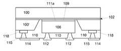
- the die 106may comprise at least one sidewall 108 , a back side 111 a and an active side 111 b .
- the back side 111 a of the die 106 comprising the DBF 109may be disposed on a portion of the etch stop layer 102 within the cavity 104 .
- the adhesive film of the DBF 109 and/or an attach processmay be used to attach the die 106 within the cavity 104 of the carrier material 100 ′.
- the carrier material 100 ′which may comprise a copper material in some cases, can be roughened to aid in the attachment of the die 106 .
- the adhesive film 119 of the DBF 109can be used as a permanent part of a final package to protect the backside 111 a of the die 106 , to provide a surface for marking, and/or to manage any warpage that may occur within the die 106 , for example.
- POP pads/land structures 118may be formed on the bottom of the carrier material 100 ′, in an embodiment ( FIG. 1 e ).
- a dielectric material 110may be formed on the carrier material 100 ′ and adjacent the die 106 and adjacent the PoP land structures 118 and within the cavity 104 of the carrier material 100 ′ ( FIG. 1 f ).
- the dielectric material 110may be formed by a laminating process, for example.
- the dielectric material 110may be formed on the bottom portion 101 of the carrier material 100 ′ comprising the cavity 104 , on the angled portion 105 of the carrier material 100 ′, and on a portion of the top portion 107 of the carrier material 100 ′ that surrounds the die 106 .
- the dielectric material 110may provide a level plane for a subsequent build-up process.
- the carrier material 100 ′may be roughened prior to lamination to aid with adhesion to the dielectric material 110 .
- vias 113may be formed in the dielectric material 110 in a die area landing of the die 106 , wherein die pads, for example copper die pads, may be exposed on the active side 111 b of the die 106 ( FIG. 1 g ).
- a semi-additive processSAP may be used to form die pad interconnect structures 112 on die pads of the die 106 and a first metal layer 114 may be formed on the dielectric material 110 adjacent the die 106 ( FIG. 1 h ).
- Interconnect structures 115may be formed to connect with the PoP structures 118 .
- Subsequent layersmay then be formed using standard substrate SAP build-up processing, for example, wherein further dielectric layers 110 ′ and metallization layers 114 ′ may be formed upon each other to form a coreless substrate portion 116 of a coreless package structure 120 by utilizing the buildup process ( FIG. 1 i ).
- the coreless package structure 120may comprise a BBUL coreless package structure 120
- the die 106may be embedded in the coreless package 120 .
- the carrier materialcomprising the top layer of the carrier material 100 , the etch stop layer 102 and the bottom layer of the carrier material 100 ′ may be removed ( FIG. 1 j ) from the coreless substrate 120 .
- the DBF 109may remain on/in the coreless substrate 120 , and may be attached/disposed onto the backside 111 a of the die 106 .
- the retained DBF 109may now serve as an EMI shield for the package 120 .
- the PoP structures 118may remain on/in the package structure 120 as well, since a portion of the PoP structures 118 are embedded in the dielectric material 110 of the coreless substrate 120 .
- a top surface 123 of the PoP structures 118may be flush/coplanar with a top surface 121 of the package 120 .
- the coreless package substrate 120may further comprise interconnect structures 125 , such as ball gird array (BGA) balls, that may be attached to the package structure 120 .
- the coreless package structure 120may comprise a fillet structure 127 of dielectric material 110 around the die 106 , wherein the dielectric material 110 may surround the sidewall 108 and the active side 111 b of the die 106 , but wherein the dielectric material 110 is absent on the back side 111 a of the die 106 , since the DBF 109 is disposed on the backside 111 b of the die 106 .
- a portion of the DBF 109may be embedded in the dielectric 110 of the coreless package 120 , and a top side of the DBF may be flush/coplanar with a top surface 128 of the filet structure 127 of the coreless package 120 , in an embodiment.
- a portion of the DBF 109may be embedded in the dielectric 110 of the coreless package 120 , and a top side of the DBF may be flush/coplanar with a top surface 128 of the filet structure 127 of the coreless package 120 , in an embodiment.
- the fillet structure 127may comprise a portion of the dielectric 110 that may be angled/raised in relation to the planar top portion 121 of the dielectric 110 of the coreless substrate 120 .
- the geometry of this fillet structure 127can be optimized to provide maximum reliability of the die/package, wherein an angle 129 of the fillet structure 127 may be varied to optimize reliability.
- FIG. 2shows a computer system according to an embodiment of the invention.
- System 200includes a processor 210 , a memory device 220 , a memory controller 230 , a graphics controller 240 , an input and output (I/O) controller 250 , a display 252 , a keyboard 254 , a pointing device 256 , and a peripheral device 258 , all of which may be communicatively coupled to each other through a bus 260 , in some embodiments.
- Processor 210may be a general purpose processor or an application specific integrated circuit (ASIC).
- I/O controller 250may include a communication module for wired or wireless communication.
- Memory device 220may be a dynamic random access memory (DRAM) device, a static random access memory (SRAM) device, a flash memory device, or a combination of these memory devices. Thus, in some embodiments, memory device 220 in system 200 does not have to include a DRAM device.
- DRAMdynamic random access memory
- SRAMstatic random access memory
- flash memory deviceor a combination of these memory devices.
- memory device 220 in system 200does not have to include a DRAM device.
- One or more of the components shown in system 200may be included in/and or may include one or more integrated circuit packages, such as the coreless package structure of FIG. 1 j , for example.
- processor 210 , or memory device 220 , or at least a portion of I/O controller 250 , or a combination of these componentsmay be included in an integrated circuit package that includes at least one embodiment of a structure, such as the various functionalized carrier material structures presented herein, described in the various embodiments.
- memory device 220may be used in some cases to provide long-term storage for the executable instructions for a method for forming packaged structures in accordance with embodiments of the present invention, and in other embodiments may be used to store on a shorter term basis the executable instructions of a method for forming package structures in accordance with embodiments of the present invention during execution by processor 210 .
- the instructionsmay be stored, or otherwise associated with, machine accessible mediums communicatively coupled with the system, such as compact disk read only memories (CD-ROMs), digital versatile disks (DVDs), and floppy disks, carrier waves, and/or other propagated signals, for example.
- memory device 220may supply the processor 210 with the executable instructions for execution.
- System 200may include computers (e.g., desktops, laptops, hand-helds, servers, Web appliances, routers, etc.), wireless communication devices (e.g., cellular phones, cordless phones, pagers, personal digital assistants, etc.), computer-related peripherals (e.g., printers, scanners, monitors, etc.), entertainment devices (e.g., televisions, radios, stereos, tape and compact disc players, video cassette recorders, camcorders, digital cameras, MP3 (Motion Picture Experts Group, Audio Layer 3) players, video games, watches, etc.), and the like.
- computerse.g., desktops, laptops, hand-helds, servers, Web appliances, routers, etc.
- wireless communication devicese.g., cellular phones, cordless phones, pagers, personal digital assistants, etc.
- computer-related peripheralse.g., printers, scanners, monitors, etc.
- entertainment devicese.g., televisions, radios, stereos, tape and
- Benefits of the embodimentsenable a new packaging architecture that can meet design requirements for future mobile/handheld system on a chip (SoC) processors at roughly half the cost of current package architectures.
- Various embodimentsenable the addition of EMI shielding into BBUL-C package structures without added post-package manufacturing cost.
- EMI shieldingmay be needed for some BBUL-C products that employ RF or other EMI generating devices containing other silicon devices sensitive to EMI.
- the filled DBFcan be used for electromagnetic interference (EMI) shielding for such RF components.
- EMIelectromagnetic interference
Landscapes
- Engineering & Computer Science (AREA)
- Physics & Mathematics (AREA)
- Microelectronics & Electronic Packaging (AREA)
- Power Engineering (AREA)
- Computer Hardware Design (AREA)
- General Physics & Mathematics (AREA)
- Condensed Matter Physics & Semiconductors (AREA)
- Manufacturing & Machinery (AREA)
- Health & Medical Sciences (AREA)
- Electromagnetism (AREA)
- Toxicology (AREA)
- Shielding Devices Or Components To Electric Or Magnetic Fields (AREA)
- Structures Or Materials For Encapsulating Or Coating Semiconductor Devices Or Solid State Devices (AREA)
Abstract
Description
As semiconductor technology advances for higher processor performance, advances in packaging architectures may include coreless bumpless build-up Layer (BBUL-C) package architectures and other such assemblies. Current process flows for BBUL-C packages involve building of the substrate on a temporary core/carrier capped with copper foil, which is etched off after the package is separated from the core.
While the specification concludes with claims particularly pointing out and distinctly claiming certain embodiments of the present invention, the advantages of this invention can be more readily ascertained from the following description of the invention when read in conjunction with the accompanying drawings in which:
In the following detailed description, reference is made to the accompanying drawings that show, by way of illustration, specific embodiments in which the methods may be practiced. These embodiments are described in sufficient detail to enable those skilled in the art to practice the embodiments. It is to be understood that the various embodiments, although different, are not necessarily mutually exclusive. For example, a particular feature, structure, or characteristic described herein, in connection with one embodiment, may be implemented within other embodiments without departing from the spirit and scope of the embodiments. In addition, it is to be understood that the location or arrangement of individual elements within each disclosed embodiment may be modified without departing from the spirit and scope of the embodiments. The following detailed description is, therefore, not to be taken in a limiting sense, and the scope of the embodiments is defined only by the appended claims, appropriately interpreted, along with the full range of equivalents to which the claims are entitled. In the drawings, like numerals refer to the same or similar functionality throughout the several views.
Methods and associated structures of forming and utilizing a microelectronic structure, such as a package structure, are described. Those methods may include forming a cavity in a carrier material, attaching a die in the cavity, wherein a backside of the die comprises a metal filled die backside film (DBF), forming a dielectric material adjacent the die and on a bottom side of the carrier material, forming a coreless substrate by building up layers on the dielectric material, and removing the carrier material from the coreless substrate. Methods of the embodiments enable the functionalizing of the DBF to create an EMI shield, for example.
In an embodiment, thecarrier material 100 may comprise two layers of a conductive material, such as but not limited to copper, for example, that may be separated by a thin etching barrier (stop)layer 102. In an embodiment, theetch stop layer 102 may comprise such materials as nickel, for example, but may comprise any such material that may serve to comprise an etch stop layer to facilitate the stopping of an etch/removal process betweencarrier layers etch stop layer 102 may serve to aid in the formation of a cavity104 (FIG. 1 b), especially during an etching process, for example. In an embodiment, athickness 103 of the bottomcarrier material layer 100′ may be dictated by the thickness and embedded depth of a die to be embedded into thecarrier material 100′ in a subsequent assembly step.
Thecavity 104 may be formed in one layer of the carrier material, such as by removing a portion of the bottomcarrier material layer 100′. Thecavity 104 may be formed utilizing any suitable removal process, such as an etching process, such as are known in the art. For example, a masking material may be laminated onto the bottom layer of thecarrier material 100′ and thecarrier material 100′ may be pattered to form thecavity 104, wherein a die may be subsequently placed therein. Theetch stop layer 102 between thecarrier material layers cavity 104 formation and may define a flat surface to place the die on to. Thecarrier material 100′ with thecavity 104 as formed may comprise abottom portion 101 anangled portion 105, and a top,flat portion 107, wherein the top portion comprises a portion of theetch stop layer 102.
In an embodiment, a die106, such as amicroelectronic die 106, for example, may comprise a die backside film (DBF)109 (FIG. 1 c). In an embodiment, the DBF may comprise a mixture of asuitable adhesive 119 and ametallic particle filler 117. Theadhesive 119 can be epoxy based in some cases. Themetallic filler 117 may comprise at least one of copper and silver, but other conductive materials may also be used, according to the particular application. A particle size of themetallic filler 117 can be chosen depending on the thickness of the DBF109 required. In an embodiment, the particle size of themetallic filler 117 may comprise less than about 10 microns.
In addition to the metallic fillers, other non-metallic fillers may also be used to improve the stiffness of the DBF109 to improve handling of the film and warpage of thedie 106 and the final packaged product. In an embodiment, the DBF109 may also comprise a glass-cloth backbone to improve stiffness. In an embodiment, the die106 may comprise athin die 106, and may comprise a thickness of below about 150 microns.
In an embodiment, the die106 may be attached to thetop portion 107 of thecarrier material 100′ comprising the cavity104 (FIG. 1 d). In an embodiment, the die106 may comprise at least onesidewall 108, aback side 111aand anactive side 111b. In an embodiment, theback side 111aof the die106 comprising the DBF109 may be disposed on a portion of theetch stop layer 102 within thecavity 104. In some cases, the adhesive film of theDBF 109 and/or an attach process may be used to attach thedie 106 within thecavity 104 of thecarrier material 100′. In an embodiment, thecarrier material 100′, which may comprise a copper material in some cases, can be roughened to aid in the attachment of the die106.
In an embodiment, theadhesive film 119 of the DBF109 can be used as a permanent part of a final package to protect thebackside 111aof thedie 106, to provide a surface for marking, and/or to manage any warpage that may occur within the die106, for example. POP pads/land structures 118 may be formed on the bottom of thecarrier material 100′, in an embodiment (FIG. 1 e).
Adielectric material 110 may be formed on thecarrier material 100′ and adjacent the die106 and adjacent thePoP land structures 118 and within thecavity 104 of thecarrier material 100′ (FIG. 1 f). In an embodiment, thedielectric material 110 may be formed by a laminating process, for example. Thedielectric material 110 may be formed on thebottom portion 101 of thecarrier material 100′ comprising thecavity 104, on theangled portion 105 of thecarrier material 100′, and on a portion of thetop portion 107 of thecarrier material 100′ that surrounds thedie 106. Thedielectric material 110 may provide a level plane for a subsequent build-up process. In an embodiment, thecarrier material 100′ may be roughened prior to lamination to aid with adhesion to thedielectric material 110.
In an embodiment,vias 113 may be formed in thedielectric material 110 in a die area landing of the die106, wherein die pads, for example copper die pads, may be exposed on theactive side 111bof the die106 (FIG. 1 g). In an embodiment, a semi-additive process (SAP) may be used to form diepad interconnect structures 112 on die pads of the die106 and afirst metal layer 114 may be formed on thedielectric material 110 adjacent the die106 (FIG. 1 h).Interconnect structures 115 may be formed to connect with thePoP structures 118. Subsequent layers may then be formed using standard substrate SAP build-up processing, for example, wherein furtherdielectric layers 110′ andmetallization layers 114′ may be formed upon each other to form acoreless substrate portion 116 of acoreless package structure 120 by utilizing the buildup process (FIG. 1 i). In an embodiment, thecoreless package structure 120 may comprise a BBULcoreless package structure 120, and the die106 may be embedded in thecoreless package 120.
In an embodiment, when the build-up is complete, the carrier material comprising the top layer of thecarrier material 100, theetch stop layer 102 and the bottom layer of thecarrier material 100′ may be removed (FIG. 1 j) from thecoreless substrate 120. The DBF109 may remain on/in thecoreless substrate 120, and may be attached/disposed onto thebackside 111aof thedie 106. The retained DBF109 may now serve as an EMI shield for thepackage 120. ThePoP structures 118 may remain on/in thepackage structure 120 as well, since a portion of thePoP structures 118 are embedded in thedielectric material 110 of thecoreless substrate 120.
Atop surface 123 of thePoP structures 118 may be flush/coplanar with atop surface 121 of thepackage 120. In an embodiment, thecoreless package substrate 120 may further compriseinterconnect structures 125, such as ball gird array (BGA) balls, that may be attached to thepackage structure 120. Thecoreless package structure 120 may comprise afillet structure 127 ofdielectric material 110 around the die106, wherein thedielectric material 110 may surround thesidewall 108 and theactive side 111bof thedie 106, but wherein thedielectric material 110 is absent on theback side 111aof the die106, since the DBF109 is disposed on thebackside 111bof the die106. A portion of theDBF 109 may be embedded in the dielectric110 of thecoreless package 120, and a top side of the DBF may be flush/coplanar with atop surface 128 of thefilet structure 127 of thecoreless package 120, in an embodiment.
is disposed on the backside111 of thedie 106. A portion of theDBF 109 may be embedded in the dielectric110 of thecoreless package 120, and a top side of the DBF may be flush/coplanar with atop surface 128 of thefilet structure 127 of thecoreless package 120, in an embodiment.
Thefillet structure 127 may comprise a portion of the dielectric110 that may be angled/raised in relation to the planartop portion 121 of the dielectric110 of thecoreless substrate 120. The geometry of thisfillet structure 127 can be optimized to provide maximum reliability of the die/package, wherein anangle 129 of thefillet structure 127 may be varied to optimize reliability.
One or more of the components shown insystem 200 may be included in/and or may include one or more integrated circuit packages, such as the coreless package structure ofFIG. 1 j, for example. For example,processor 210, ormemory device 220, or at least a portion of I/O controller 250, or a combination of these components may be included in an integrated circuit package that includes at least one embodiment of a structure, such as the various functionalized carrier material structures presented herein, described in the various embodiments.
These elements perform their conventional functions well known in the art. In particular,memory device 220 may be used in some cases to provide long-term storage for the executable instructions for a method for forming packaged structures in accordance with embodiments of the present invention, and in other embodiments may be used to store on a shorter term basis the executable instructions of a method for forming package structures in accordance with embodiments of the present invention during execution byprocessor 210. In addition, the instructions may be stored, or otherwise associated with, machine accessible mediums communicatively coupled with the system, such as compact disk read only memories (CD-ROMs), digital versatile disks (DVDs), and floppy disks, carrier waves, and/or other propagated signals, for example. In one embodiment,memory device 220 may supply theprocessor 210 with the executable instructions for execution.
Benefits of the embodiments enable a new packaging architecture that can meet design requirements for future mobile/handheld system on a chip (SoC) processors at roughly half the cost of current package architectures. Various embodiments enable the addition of EMI shielding into BBUL-C package structures without added post-package manufacturing cost. EMI shielding may be needed for some BBUL-C products that employ RF or other EMI generating devices containing other silicon devices sensitive to EMI. By functionalizing the DBF by filling it with metallic particles, the filled DBF can be used for electromagnetic interference (EMI) shielding for such RF components.
Although the foregoing description has specified certain steps and materials that may be used in the method of the present invention, those skilled in the art will appreciate that many modifications and substitutions may be made. Accordingly, it is intended that all such modifications, alterations, substitutions and additions be considered to fall within the spirit and scope of the invention as defined by the appended claims. In addition, it is appreciated that various microelectronic structures, such as package structures, are well known in the art. Therefore, the Figures provided herein illustrate only portions of an exemplary microelectronic device that pertains to the practice of the present invention. Thus the present invention is not limited to the structures described herein.
Claims (16)
1. A structure comprising:
a die embedded in a coreless substrate, wherein the coreless substrate includes; a dielectric material adjacent the die, and wherein the dielectric material includes a fillet portion;
die pad interconnect structures disposed in a die pad area of the die; and
a DBF disposed on a backside of the die, wherein a top surface of the DBF is coplanar with a top surface of the fillet portion.
2. The structure ofclaim 1 wherein the DBF comprises an EMI shield.
3. The structure ofclaim 1 wherein the coreless substrate comprises a portion of a coreless bumpless buildup package structure.
4. The structure ofclaim 1 wherein the DBF comprises an adhesive.
5. The structure ofclaim 1 wherein the DBF comprises metallic filler particles.
6. The structure ofclaim 5 wherein metallic filler particles comprise at least one of copper and silver.
7. The structure ofclaim 5 wherein the metallic filler particles comprise a particle size of less than about 10 microns.
8. A structure comprising:
a die embedded in a coreless substrate, wherein the coreless substrate includes a dielectric material adjacent the die, and wherein the dielectric material includes a fillet portion;
a DBF is disposed on a backside of the die, wherein a top surface of the DBF is coplanar with a top surface of the fillet portion;
die pad interconnect structures disposed in a die pad area of the die; and
vias in the coreless substrate disposed in a non-die area that are connected to PoP lands, wherein the PoP lands are disposed within the coreless substrate adjacent the die, and wherein a top surface of the PoP lands is coplanar with a top surface of the coreless substrate.
9. The structure ofclaim 7 wherein the DBF comprises an EMI shield.
10. The structure ofclaim 7 wherein the coreless substrate comprises a portion of a coreless bumpless buildup package structure.
11. The structure ofclaim 10 wherein the die is fully embedded in the coreless bumpless buildup package.
12. The structure ofclaim 11 wherein a portion of the DBF is embedded in the coreless bumpless buildup package.
13. The structure ofclaim 7 wherein the DBF comprises metallic particles.
14. The structure ofclaim 13 wherein the coreless bumpless buildup package comprises RF components.
15. The structure ofclaim 8 further comprising a system comprising:
a bus is communicatively coupled to the structure; and
a DRAM communicatively coupled to the bus.
16. The structure ofclaim 8 wherein the DBF comprises a glass cloth backbone.
Priority Applications (8)
| Application Number | Priority Date | Filing Date | Title |
|---|---|---|---|
| US12/755,201US8319318B2 (en) | 2010-04-06 | 2010-04-06 | Forming metal filled die back-side film for electromagnetic interference shielding with coreless packages |
| EP11766549.7AEP2556534B1 (en) | 2010-04-06 | 2011-04-04 | Forming metal filled die back-side film for electromagnetic interference shielding with coreless packages |
| PCT/US2011/031079WO2011126973A2 (en) | 2010-04-06 | 2011-04-04 | Forming metal filled die back-side film for electromagnetic interference shielding with coreless packages |
| KR1020127025222AKR101409094B1 (en) | 2010-04-06 | 2011-04-04 | Forming metal filled die back-side film for electromagnetic interference shielding with coreless packages |
| JP2013500250AJP5599934B2 (en) | 2010-04-06 | 2011-04-04 | Method for forming metal filled die backside film for electromagnetic interference shield with coreless package |
| CN201180017635.7ACN102822963B (en) | 2010-04-06 | 2011-04-04 | Centreless packaging part is utilized to form the metal filled die backside thin film for electromagnetic interference shield |
| TW100111819ATWI521667B (en) | 2010-04-06 | 2011-04-06 | Forming metal filled die back-side film for electromagnetic interference shielding with coreless packages |
| US13/660,095US8507324B2 (en) | 2010-04-06 | 2012-10-25 | Forming metal filled die back-side film for electromagnetic interference shielding with coreless packages |
Applications Claiming Priority (1)
| Application Number | Priority Date | Filing Date | Title |
|---|---|---|---|
| US12/755,201US8319318B2 (en) | 2010-04-06 | 2010-04-06 | Forming metal filled die back-side film for electromagnetic interference shielding with coreless packages |
Related Child Applications (1)
| Application Number | Title | Priority Date | Filing Date |
|---|---|---|---|
| US13/660,095DivisionUS8507324B2 (en) | 2010-04-06 | 2012-10-25 | Forming metal filled die back-side film for electromagnetic interference shielding with coreless packages |
Publications (2)
| Publication Number | Publication Date |
|---|---|
| US20110241186A1 US20110241186A1 (en) | 2011-10-06 |
| US8319318B2true US8319318B2 (en) | 2012-11-27 |
Family
ID=44708674
Family Applications (2)
| Application Number | Title | Priority Date | Filing Date |
|---|---|---|---|
| US12/755,201Active2030-10-10US8319318B2 (en) | 2010-04-06 | 2010-04-06 | Forming metal filled die back-side film for electromagnetic interference shielding with coreless packages |
| US13/660,095Expired - Fee RelatedUS8507324B2 (en) | 2010-04-06 | 2012-10-25 | Forming metal filled die back-side film for electromagnetic interference shielding with coreless packages |
Family Applications After (1)
| Application Number | Title | Priority Date | Filing Date |
|---|---|---|---|
| US13/660,095Expired - Fee RelatedUS8507324B2 (en) | 2010-04-06 | 2012-10-25 | Forming metal filled die back-side film for electromagnetic interference shielding with coreless packages |
Country Status (7)
| Country | Link |
|---|---|
| US (2) | US8319318B2 (en) |
| EP (1) | EP2556534B1 (en) |
| JP (1) | JP5599934B2 (en) |
| KR (1) | KR101409094B1 (en) |
| CN (1) | CN102822963B (en) |
| TW (1) | TWI521667B (en) |
| WO (1) | WO2011126973A2 (en) |
Cited By (22)
| Publication number | Priority date | Publication date | Assignee | Title |
|---|---|---|---|---|
| US20130003319A1 (en)* | 2011-06-30 | 2013-01-03 | Pramod Malatkar | Bumpless build-up layer package warpage reduction |
| US8507324B2 (en) | 2010-04-06 | 2013-08-13 | Intel Corporation | Forming metal filled die back-side film for electromagnetic interference shielding with coreless packages |
| US20130249104A1 (en)* | 2012-03-20 | 2013-09-26 | Stats Chippac, Ltd. | Semiconductor Device and Method of Forming Conductive Layer Over Metal Substrate for Electrical Interconnect of Semiconductor Die |
| US8580616B2 (en) | 2010-09-24 | 2013-11-12 | Intel Corporation | Methods of forming fully embedded bumpless build-up layer packages and structures formed thereby |
| US20140110866A1 (en)* | 2010-07-26 | 2014-04-24 | General Electric Company | System and method of chip package build-up |
| US8937382B2 (en) | 2011-06-27 | 2015-01-20 | Intel Corporation | Secondary device integration into coreless microelectronic device packages |
| US8969140B2 (en) | 2010-04-02 | 2015-03-03 | Intel Corporation | Embedded semiconductive chips in reconstituted wafers, and systems containing same |
| US8987065B2 (en) | 2010-04-16 | 2015-03-24 | Intel Corporation | Forming functionalized carrier structures with coreless packages |
| US9147669B2 (en) | 2009-12-29 | 2015-09-29 | Intel Corporation | Recessed and embedded die coreless package |
| US9257368B2 (en) | 2012-05-14 | 2016-02-09 | Intel Corporation | Microelectric package utilizing multiple bumpless build-up structures and through-silicon vias |
| US9266723B2 (en) | 2010-07-06 | 2016-02-23 | Intel Corporation | Misalignment correction for embedded microelectronic die applications |
| US9362253B2 (en) | 2010-08-26 | 2016-06-07 | Intel Corporation | Bumpless build-up layer package with pre-stacked microelectronic devices |
| US9425156B2 (en) | 2013-07-29 | 2016-08-23 | Samsung Electronics Co., Ltd. | Semiconductor packages having semiconductor chips disposed in opening in shielding core plate |
| US9530718B2 (en) | 2012-12-26 | 2016-12-27 | Intel Corporation | DBF film as a thermal interface material |
| US9601445B2 (en) | 2014-11-26 | 2017-03-21 | Samsung Electronics Co., Ltd. | Semiconductor packages |
| US9653438B2 (en) | 2014-08-21 | 2017-05-16 | General Electric Company | Electrical interconnect structure for an embedded semiconductor device package and method of manufacturing thereof |
| US9685390B2 (en) | 2012-06-08 | 2017-06-20 | Intel Corporation | Microelectronic package having non-coplanar, encapsulated microelectronic devices and a bumpless build-up layer |
| US9818719B2 (en) | 2010-06-30 | 2017-11-14 | Intel Corporation | Bumpless build-up layer package design with an interposer |
| US9847308B2 (en) | 2010-04-28 | 2017-12-19 | Intel Corporation | Magnetic intermetallic compound interconnect |
| US9929131B2 (en) | 2015-12-18 | 2018-03-27 | Samsung Electronics Co., Ltd. | Method of fabricating a semiconductor package having mold layer with curved corner |
| US11116083B2 (en)* | 2016-03-31 | 2021-09-07 | At&S (China) Co. Ltd. | Electronic component embedded by laminate sheet |
| US11189573B2 (en)* | 2016-03-31 | 2021-11-30 | Intel Corporation | Semiconductor package with electromagnetic interference shielding using metal layers and vias |
Families Citing this family (25)
| Publication number | Priority date | Publication date | Assignee | Title |
|---|---|---|---|---|
| US8901724B2 (en)* | 2009-12-29 | 2014-12-02 | Intel Corporation | Semiconductor package with embedded die and its methods of fabrication |
| US8431438B2 (en) | 2010-04-06 | 2013-04-30 | Intel Corporation | Forming in-situ micro-feature structures with coreless packages |
| US8939347B2 (en) | 2010-04-28 | 2015-01-27 | Intel Corporation | Magnetic intermetallic compound interconnect |
| US8313958B2 (en) | 2010-05-12 | 2012-11-20 | Intel Corporation | Magnetic microelectronic device attachment |
| US8434668B2 (en) | 2010-05-12 | 2013-05-07 | Intel Corporation | Magnetic attachment structure |
| US8609532B2 (en) | 2010-05-26 | 2013-12-17 | Intel Corporation | Magnetically sintered conductive via |
| TWI538071B (en)* | 2010-11-16 | 2016-06-11 | 星科金朋有限公司 | Integrated circuit packaging system with connection structure and method of manufacture thereof |
| US8581421B2 (en)* | 2010-12-20 | 2013-11-12 | Shinko Electric Industries Co., Ltd. | Semiconductor package manufacturing method and semiconductor package |
| US8421245B2 (en) | 2010-12-22 | 2013-04-16 | Intel Corporation | Substrate with embedded stacked through-silicon via die |
| WO2013074061A1 (en)* | 2011-11-14 | 2013-05-23 | Intel Corporation | Controlled solder-on-die integrations on packages and methods of assembling same |
| WO2013089754A1 (en)* | 2011-12-15 | 2013-06-20 | Intel Corporation | Packaged semiconductor die with bumpless die-package interface for bumpless build-up layer (bbul) packages |
| CN104160497B (en) | 2011-12-20 | 2017-10-27 | 英特尔公司 | Microelectronics Packaging and stacking micromodule and the computing system including the encapsulation and component |
| WO2013095405A1 (en)* | 2011-12-20 | 2013-06-27 | Intel Corporation | Enabling package-on-package (pop) pad surface finishes on bumpless build-up layer (bbul) package |
| JP6092555B2 (en)* | 2012-09-24 | 2017-03-08 | 新光電気工業株式会社 | Wiring board manufacturing method |
| US20140175657A1 (en)* | 2012-12-21 | 2014-06-26 | Mihir A. Oka | Methods to improve laser mark contrast on die backside film in embedded die packages |
| CN104299919B (en)* | 2013-07-15 | 2017-05-24 | 碁鼎科技秦皇岛有限公司 | Coreless package structure and method for manufacturing the same |
| US9985010B2 (en)* | 2015-05-22 | 2018-05-29 | Qualcomm Incorporated | System, apparatus, and method for embedding a device in a faceup workpiece |
| WO2016187748A1 (en)* | 2015-05-22 | 2016-12-01 | 3M Innovative Properties Company | Viscoelastic electromagnetic interference (emi), shock and vibration absorber and methods of making the same |
| US9811627B2 (en)* | 2015-12-08 | 2017-11-07 | Taiwan Semiconductor Manufacturing Co., Ltd. | Method of component partitions on system on chip and device thereof |
| US10541209B2 (en)* | 2017-08-03 | 2020-01-21 | General Electric Company | Electronics package including integrated electromagnetic interference shield and method of manufacturing thereof |
| US10541153B2 (en) | 2017-08-03 | 2020-01-21 | General Electric Company | Electronics package with integrated interconnect structure and method of manufacturing thereof |
| US10804115B2 (en) | 2017-08-03 | 2020-10-13 | General Electric Company | Electronics package with integrated interconnect structure and method of manufacturing thereof |
| KR102504293B1 (en) | 2017-11-29 | 2023-02-27 | 삼성전자 주식회사 | Package on package type semiconductor package |
| US12394683B2 (en)* | 2020-03-18 | 2025-08-19 | Advanced Micro Devices, Inc. | Molded semiconductor chip package with stair-step molding layer |
| US11398445B2 (en) | 2020-05-29 | 2022-07-26 | General Electric Company | Mechanical punched via formation in electronics package and electronics package formed thereby |
Citations (61)
| Publication number | Priority date | Publication date | Assignee | Title |
|---|---|---|---|---|
| US5151769A (en)* | 1991-04-04 | 1992-09-29 | General Electric Company | Optically patterned RF shield for an integrated circuit chip for analog and/or digital operation at microwave frequencies |
| US5353498A (en) | 1993-02-08 | 1994-10-11 | General Electric Company | Method for fabricating an integrated circuit module |
| US5355102A (en)* | 1990-04-05 | 1994-10-11 | General Electric Company | HDI impedance matched microwave circuit assembly |
| US5527741A (en) | 1994-10-11 | 1996-06-18 | Martin Marietta Corporation | Fabrication and structures of circuit modules with flexible interconnect layers |
| US5841193A (en) | 1996-05-20 | 1998-11-24 | Epic Technologies, Inc. | Single chip modules, repairable multichip modules, and methods of fabrication thereof |
| US6154366A (en) | 1999-11-23 | 2000-11-28 | Intel Corporation | Structures and processes for fabricating moisture resistant chip-on-flex packages |
| US6239482B1 (en) | 1999-06-21 | 2001-05-29 | General Electric Company | Integrated circuit package including window frame |
| US6242282B1 (en) | 1999-10-04 | 2001-06-05 | General Electric Company | Circuit chip package and fabrication method |
| US6271469B1 (en) | 1999-11-12 | 2001-08-07 | Intel Corporation | Direct build-up layer on an encapsulated die package |
| US6306680B1 (en) | 1999-02-22 | 2001-10-23 | General Electric Company | Power overlay chip scale packages for discrete power devices |
| US6396148B1 (en) | 2000-02-10 | 2002-05-28 | Epic Technologies, Inc. | Electroless metal connection structures and methods |
| US6423570B1 (en) | 2000-10-18 | 2002-07-23 | Intel Corporation | Method to protect an encapsulated die package during back grinding with a solder metallization layer and devices formed thereby |
| US6426545B1 (en) | 2000-02-10 | 2002-07-30 | Epic Technologies, Inc. | Integrated circuit structures and methods employing a low modulus high elongation photodielectric |
| US6489185B1 (en) | 2000-09-13 | 2002-12-03 | Intel Corporation | Protective film for the fabrication of direct build-up layers on an encapsulated die package |
| US6555906B2 (en) | 2000-12-15 | 2003-04-29 | Intel Corporation | Microelectronic package having a bumpless laminated interconnection layer |
| US6555908B1 (en) | 2000-02-10 | 2003-04-29 | Epic Technologies, Inc. | Compliant, solderable input/output bump structures |
| US6580611B1 (en) | 2001-12-21 | 2003-06-17 | Intel Corporation | Dual-sided heat removal system |
| US6586836B1 (en) | 2000-03-01 | 2003-07-01 | Intel Corporation | Process for forming microelectronic packages and intermediate structures formed therewith |
| US6586822B1 (en) | 2000-09-08 | 2003-07-01 | Intel Corporation | Integrated core microelectronic package |
| US6586276B2 (en) | 2001-07-11 | 2003-07-01 | Intel Corporation | Method for fabricating a microelectronic device using wafer-level adhesion layer deposition |
| US6617682B1 (en) | 2000-09-28 | 2003-09-09 | Intel Corporation | Structure for reducing die corner and edge stresses in microelectronic packages |
| US6703400B2 (en) | 2001-02-23 | 2004-03-09 | Schering Corporation | Methods for treating multidrug resistance |
| US6706553B2 (en) | 2001-03-26 | 2004-03-16 | Intel Corporation | Dispensing process for fabrication of microelectronic packages |
| US6709898B1 (en) | 2000-10-04 | 2004-03-23 | Intel Corporation | Die-in-heat spreader microelectronic package |
| US6713859B1 (en) | 2000-09-13 | 2004-03-30 | Intel Corporation | Direct build-up layer on an encapsulated die package having a moisture barrier structure |
| US6734534B1 (en) | 2000-08-16 | 2004-05-11 | Intel Corporation | Microelectronic substrate with integrated devices |
| US6838748B2 (en)* | 2002-05-22 | 2005-01-04 | Sharp Kabushiki Kaisha | Semiconductor element with electromagnetic shielding layer on back/side face(s) thereof |
| US6841413B2 (en) | 2002-01-07 | 2005-01-11 | Intel Corporation | Thinned die integrated circuit package |
| US6888240B2 (en) | 2001-04-30 | 2005-05-03 | Intel Corporation | High performance, low cost microelectronic circuit package with interposer |
| US6894399B2 (en) | 2001-04-30 | 2005-05-17 | Intel Corporation | Microelectronic device having signal distribution functionality on an interfacial layer thereof |
| US20050258537A1 (en) | 2003-05-14 | 2005-11-24 | Siliconware Precision Industries Co., Ltd. | Semiconductor package with build-up layers formed on chip and fabrication method of the semiconductor package |
| JP2006059863A (en) | 2004-08-17 | 2006-03-02 | Cmk Corp | Package substrate and manufacturing method thereof |
| US20060125080A1 (en) | 2004-12-09 | 2006-06-15 | Phoenix Precision Technology Corporation | Semiconductor package structure and method for fabricating the same |
| US7071024B2 (en) | 2001-05-21 | 2006-07-04 | Intel Corporation | Method for packaging a microelectronic device using on-die bond pad expansion |
| US7078788B2 (en) | 2000-08-16 | 2006-07-18 | Intel Corporation | Microelectronic substrates with integrated devices |
| US20060186536A1 (en) | 2005-02-02 | 2006-08-24 | Shih-Ping Hsu | Substrate assembly with direct electrical connection as a semiconductor package |
| US7109055B2 (en) | 2005-01-20 | 2006-09-19 | Freescale Semiconductor, Inc. | Methods and apparatus having wafer level chip scale package for sensing elements |
| US7160755B2 (en) | 2005-04-18 | 2007-01-09 | Freescale Semiconductor, Inc. | Method of forming a substrateless semiconductor package |
| US7183658B2 (en) | 2001-09-05 | 2007-02-27 | Intel Corporation | Low cost microelectronic circuit package |
| US7262444B2 (en)* | 2005-08-17 | 2007-08-28 | General Electric Company | Power semiconductor packaging method and structure |
| US20080192776A1 (en) | 2007-02-09 | 2008-08-14 | Fleming Kristoffer D | Mechanism for increasing UWB MAC efficiency and bandwidth via the period inclusion of PHY preambles for synchronization |
| US7425464B2 (en) | 2006-03-10 | 2008-09-16 | Freescale Semiconductor, Inc. | Semiconductor device packaging |
| US7442581B2 (en) | 2004-12-10 | 2008-10-28 | Freescale Semiconductor, Inc. | Flexible carrier and release method for high volume electronic package fabrication |
| US20080315391A1 (en) | 2007-06-25 | 2008-12-25 | Epic Technologies, Inc. | Integrated structures and methods of fabrication thereof with fan-out metallization on a chips-first chip layer |
| US20090007282A1 (en) | 1998-08-21 | 2009-01-01 | Kirin Pharma Kabushiki Kaisha | Method for modifying chromosomes |
| US7476563B2 (en) | 2006-11-17 | 2009-01-13 | Freescale Semiconductor, Inc. | Method of packaging a device using a dielectric layer |
| US20090072382A1 (en) | 2007-09-18 | 2009-03-19 | Guzek John S | Microelectronic package and method of forming same |
| US20090079063A1 (en) | 2007-09-26 | 2009-03-26 | Chrysler Gregory M | Microelectronic package and method of cooling an interconnect feature in same |
| US20090079064A1 (en) | 2007-09-25 | 2009-03-26 | Jiamiao Tang | Methods of forming a thin tim coreless high density bump-less package and structures formed thereby |
| US20090212416A1 (en) | 2008-02-22 | 2009-08-27 | Skeete Oswald L | Integrated circuit package and method of manufacturing same |
| US7588951B2 (en) | 2006-11-17 | 2009-09-15 | Freescale Semiconductor, Inc. | Method of packaging a semiconductor device and a prefabricated connector |
| US7595226B2 (en) | 2007-08-29 | 2009-09-29 | Freescale Semiconductor, Inc. | Method of packaging an integrated circuit die |
| US20090294942A1 (en) | 2008-06-03 | 2009-12-03 | Palmer Eric C | Package on package using a bump-less build up layer (bbul) package |
| US7632715B2 (en) | 2007-01-05 | 2009-12-15 | Freescale Semiconductor, Inc. | Method of packaging semiconductor devices |
| US7648858B2 (en) | 2007-06-19 | 2010-01-19 | Freescale Semiconductor, Inc. | Methods and apparatus for EMI shielding in multi-chip modules |
| US7651889B2 (en) | 2007-09-13 | 2010-01-26 | Freescale Semiconductor, Inc. | Electromagnetic shield formation for integrated circuit die package |
| US7659143B2 (en) | 2006-09-29 | 2010-02-09 | Intel Corporation | Dual-chip integrated heat spreader assembly, packages containing same, and systems containing same |
| US7723164B2 (en) | 2006-09-01 | 2010-05-25 | Intel Corporation | Dual heat spreader panel assembly method for bumpless die-attach packages, packages containing same, and systems containing same |
| US20100237477A1 (en)* | 2009-03-23 | 2010-09-23 | Stats Chippac, Ltd. | Semiconductor Device and Method of Mounting Pre-Fabricated Shielding Frame over Semiconductor Die |
| US20100278705A1 (en)* | 2008-05-12 | 2010-11-04 | Secretary, Dept. of Atomic Energy Gov't of India Anushakti Bhavan Chatrapathi Shivaji Maharaj Marg | Innovative cut-and-feed operation for enhancing the performance of ion-exchange chromatographic separation |
| WO2011126973A2 (en) | 2010-04-06 | 2011-10-13 | Intel Corporation | Forming metal filled die back-side film for electromagnetic interference shielding with coreless packages |
Family Cites Families (37)
| Publication number | Priority date | Publication date | Assignee | Title |
|---|---|---|---|---|
| JPH01258458A (en)* | 1988-04-08 | 1989-10-16 | Nec Corp | Wafer integration type integrated circuit |
| JPH04261029A (en)* | 1991-02-13 | 1992-09-17 | Hitachi Ltd | Pellet attachment method |
| US6740959B2 (en)* | 2001-08-01 | 2004-05-25 | International Business Machines Corporation | EMI shielding for semiconductor chip carriers |
| JP4094494B2 (en)* | 2002-08-23 | 2008-06-04 | 新光電気工業株式会社 | Semiconductor package |
| TWM249376U (en)* | 2003-11-06 | 2004-11-01 | Chipmos Technologies Inc | Image sensor with low noise |
| JP4271590B2 (en)* | 2004-01-20 | 2009-06-03 | 新光電気工業株式会社 | Semiconductor device and manufacturing method thereof |
| JP2006032379A (en)* | 2004-07-12 | 2006-02-02 | Akita Denshi Systems:Kk | Laminate semiconductor device and its manufacturing method |
| JP2006066612A (en)* | 2004-08-26 | 2006-03-09 | Seiko Epson Corp | Flip mounted high frequency module |
| CN101996962B (en)* | 2004-10-28 | 2013-01-16 | 京瓷株式会社 | Electronic component module and radio communications equipment |
| JP4602208B2 (en) | 2004-12-15 | 2010-12-22 | 新光電気工業株式会社 | Electronic component mounting structure and manufacturing method thereof |
| JP4810836B2 (en)* | 2005-02-14 | 2011-11-09 | 住友ベークライト株式会社 | Adhesive, semiconductor device, and method for manufacturing semiconductor device |
| JP4452222B2 (en)* | 2005-09-07 | 2010-04-21 | 新光電気工業株式会社 | Multilayer wiring board and manufacturing method thereof |
| JP2008010705A (en)* | 2006-06-30 | 2008-01-17 | Phoenix Precision Technology Corp | Package structure of chip built-in substrate |
| US8293584B2 (en)* | 2006-08-04 | 2012-10-23 | Stats Chippac Ltd. | Integrated circuit package system with filled wafer recess |
| DE102007020656B4 (en)* | 2007-04-30 | 2009-05-07 | Infineon Technologies Ag | Semiconductor chip workpiece, semiconductor device, and method of manufacturing a semiconductor chip workpiece |
| US8039309B2 (en)* | 2007-05-10 | 2011-10-18 | Texas Instruments Incorporated | Systems and methods for post-circuitization assembly |
| CN101689516B (en)* | 2007-06-28 | 2011-09-14 | 松下电器产业株式会社 | Method for manufacturing the semiconductor element mounting structure and pressurizing tool |
| US9941245B2 (en) | 2007-09-25 | 2018-04-10 | Intel Corporation | Integrated circuit packages including high density bump-less build up layers and a lesser density core or coreless substrate |
| JP5314889B2 (en)* | 2007-12-27 | 2013-10-16 | 新光電気工業株式会社 | Electronic device, manufacturing method thereof, wiring board, and manufacturing method thereof |
| JP5224845B2 (en)* | 2008-02-18 | 2013-07-03 | 新光電気工業株式会社 | Semiconductor device manufacturing method and semiconductor device |
| US8058723B2 (en)* | 2008-03-19 | 2011-11-15 | Phoenix Precision Technology Corporation | Package structure in which coreless substrate has direct electrical connections to semiconductor chip and manufacturing method thereof |
| US20110108999A1 (en) | 2009-11-06 | 2011-05-12 | Nalla Ravi K | Microelectronic package and method of manufacturing same |
| US8901724B2 (en) | 2009-12-29 | 2014-12-02 | Intel Corporation | Semiconductor package with embedded die and its methods of fabrication |
| US8742561B2 (en) | 2009-12-29 | 2014-06-03 | Intel Corporation | Recessed and embedded die coreless package |
| US8891246B2 (en) | 2010-03-17 | 2014-11-18 | Intel Corporation | System-in-package using embedded-die coreless substrates, and processes of forming same |
| US8535989B2 (en) | 2010-04-02 | 2013-09-17 | Intel Corporation | Embedded semiconductive chips in reconstituted wafers, and systems containing same |
| US8431438B2 (en) | 2010-04-06 | 2013-04-30 | Intel Corporation | Forming in-situ micro-feature structures with coreless packages |
| US8618652B2 (en) | 2010-04-16 | 2013-12-31 | Intel Corporation | Forming functionalized carrier structures with coreless packages |
| US8313958B2 (en) | 2010-05-12 | 2012-11-20 | Intel Corporation | Magnetic microelectronic device attachment |
| US20110316140A1 (en) | 2010-06-29 | 2011-12-29 | Nalla Ravi K | Microelectronic package and method of manufacturing same |
| US20120001339A1 (en) | 2010-06-30 | 2012-01-05 | Pramod Malatkar | Bumpless build-up layer package design with an interposer |
| US8372666B2 (en) | 2010-07-06 | 2013-02-12 | Intel Corporation | Misalignment correction for embedded microelectronic die applications |
| US8304913B2 (en)* | 2010-09-24 | 2012-11-06 | Intel Corporation | Methods of forming fully embedded bumpless build-up layer packages and structures formed thereby |
| US8786066B2 (en) | 2010-09-24 | 2014-07-22 | Intel Corporation | Die-stacking using through-silicon vias on bumpless build-up layer substrates including embedded-dice, and processes of forming same |
| US20120112336A1 (en) | 2010-11-05 | 2012-05-10 | Guzek John S | Encapsulated die, microelectronic package containing same, and method of manufacturing said microelectronic package |
| US20120139095A1 (en) | 2010-12-03 | 2012-06-07 | Manusharow Mathew J | Low-profile microelectronic package, method of manufacturing same, and electronic assembly containing same |
| US8508037B2 (en) | 2010-12-07 | 2013-08-13 | Intel Corporation | Bumpless build-up layer and laminated core hybrid structures and methods of assembling same |
- 2010
- 2010-04-06USUS12/755,201patent/US8319318B2/enactiveActive
- 2011
- 2011-04-04CNCN201180017635.7Apatent/CN102822963B/enactiveActive
- 2011-04-04JPJP2013500250Apatent/JP5599934B2/enactiveActive
- 2011-04-04KRKR1020127025222Apatent/KR101409094B1/ennot_activeExpired - Fee Related
- 2011-04-04EPEP11766549.7Apatent/EP2556534B1/enactiveActive
- 2011-04-04WOPCT/US2011/031079patent/WO2011126973A2/enactiveApplication Filing
- 2011-04-06TWTW100111819Apatent/TWI521667B/enactive
- 2012
- 2012-10-25USUS13/660,095patent/US8507324B2/ennot_activeExpired - Fee Related
Patent Citations (80)
| Publication number | Priority date | Publication date | Assignee | Title |
|---|---|---|---|---|
| US5355102A (en)* | 1990-04-05 | 1994-10-11 | General Electric Company | HDI impedance matched microwave circuit assembly |
| US5151769A (en)* | 1991-04-04 | 1992-09-29 | General Electric Company | Optically patterned RF shield for an integrated circuit chip for analog and/or digital operation at microwave frequencies |
| US5353498A (en) | 1993-02-08 | 1994-10-11 | General Electric Company | Method for fabricating an integrated circuit module |
| US5497033A (en) | 1993-02-08 | 1996-03-05 | Martin Marietta Corporation | Embedded substrate for integrated circuit modules |
| US5527741A (en) | 1994-10-11 | 1996-06-18 | Martin Marietta Corporation | Fabrication and structures of circuit modules with flexible interconnect layers |
| US5841193A (en) | 1996-05-20 | 1998-11-24 | Epic Technologies, Inc. | Single chip modules, repairable multichip modules, and methods of fabrication thereof |
| US6159767A (en) | 1996-05-20 | 2000-12-12 | Epic Technologies, Inc. | Single chip modules, repairable multichip modules, and methods of fabrication thereof |
| US20090007282A1 (en) | 1998-08-21 | 2009-01-01 | Kirin Pharma Kabushiki Kaisha | Method for modifying chromosomes |
| US6306680B1 (en) | 1999-02-22 | 2001-10-23 | General Electric Company | Power overlay chip scale packages for discrete power devices |
| US6239482B1 (en) | 1999-06-21 | 2001-05-29 | General Electric Company | Integrated circuit package including window frame |
| US6242282B1 (en) | 1999-10-04 | 2001-06-05 | General Electric Company | Circuit chip package and fabrication method |
| US6396153B2 (en) | 1999-10-04 | 2002-05-28 | General Electric Company | Circuit chip package and fabrication method |
| US6271469B1 (en) | 1999-11-12 | 2001-08-07 | Intel Corporation | Direct build-up layer on an encapsulated die package |
| US6154366A (en) | 1999-11-23 | 2000-11-28 | Intel Corporation | Structures and processes for fabricating moisture resistant chip-on-flex packages |
| US6396148B1 (en) | 2000-02-10 | 2002-05-28 | Epic Technologies, Inc. | Electroless metal connection structures and methods |
| US6818544B2 (en) | 2000-02-10 | 2004-11-16 | Epic Technologies, Inc. | Compliant, solderable input/output bump structures |
| US6426545B1 (en) | 2000-02-10 | 2002-07-30 | Epic Technologies, Inc. | Integrated circuit structures and methods employing a low modulus high elongation photodielectric |
| US7112467B2 (en) | 2000-02-10 | 2006-09-26 | Epic Technologies, Inc. | Structure and method for temporarily holding integrated circuit chips in accurate alignment |
| US6555908B1 (en) | 2000-02-10 | 2003-04-29 | Epic Technologies, Inc. | Compliant, solderable input/output bump structures |
| US7189596B1 (en) | 2000-03-01 | 2007-03-13 | Intel Corporation | Process for forming a direct build-up layer on an encapsulated die packages utilizing intermediate structures |
| US6586836B1 (en) | 2000-03-01 | 2003-07-01 | Intel Corporation | Process for forming microelectronic packages and intermediate structures formed therewith |
| US7078788B2 (en) | 2000-08-16 | 2006-07-18 | Intel Corporation | Microelectronic substrates with integrated devices |
| US6734534B1 (en) | 2000-08-16 | 2004-05-11 | Intel Corporation | Microelectronic substrate with integrated devices |
| US6586822B1 (en) | 2000-09-08 | 2003-07-01 | Intel Corporation | Integrated core microelectronic package |
| US6825063B2 (en) | 2000-09-08 | 2004-11-30 | Intel Corporation | Integrated core microelectronic package |
| US7416918B2 (en) | 2000-09-13 | 2008-08-26 | Intel Corporation | Direct build-up layer on an encapsulated die package having a moisture barrier structure |
| US6489185B1 (en) | 2000-09-13 | 2002-12-03 | Intel Corporation | Protective film for the fabrication of direct build-up layers on an encapsulated die package |
| US6713859B1 (en) | 2000-09-13 | 2004-03-30 | Intel Corporation | Direct build-up layer on an encapsulated die package having a moisture barrier structure |
| US6617682B1 (en) | 2000-09-28 | 2003-09-09 | Intel Corporation | Structure for reducing die corner and edge stresses in microelectronic packages |
| US6794223B2 (en) | 2000-09-28 | 2004-09-21 | Intel Corporation | Structure and process for reducing die corner and edge stresses in microelectronic packages |
| US6709898B1 (en) | 2000-10-04 | 2004-03-23 | Intel Corporation | Die-in-heat spreader microelectronic package |
| US6902950B2 (en) | 2000-10-18 | 2005-06-07 | Intel Corporation | Method to protect an encapsulated die package during back grinding with a solder metallization layer and devices formed thereby |
| US6423570B1 (en) | 2000-10-18 | 2002-07-23 | Intel Corporation | Method to protect an encapsulated die package during back grinding with a solder metallization layer and devices formed thereby |
| US6964889B2 (en) | 2000-10-18 | 2005-11-15 | Intel Corporation | Method to protect an encapsulated die package during back grinding with a solder metallization layer and devices formed thereby |
| US6555906B2 (en) | 2000-12-15 | 2003-04-29 | Intel Corporation | Microelectronic package having a bumpless laminated interconnection layer |
| US7067356B2 (en) | 2000-12-15 | 2006-06-27 | Intel Corporation | Method of fabricating microelectronic package having a bumpless laminated interconnection layer |
| US6703400B2 (en) | 2001-02-23 | 2004-03-09 | Schering Corporation | Methods for treating multidrug resistance |
| US6706553B2 (en) | 2001-03-26 | 2004-03-16 | Intel Corporation | Dispensing process for fabrication of microelectronic packages |
| US6888240B2 (en) | 2001-04-30 | 2005-05-03 | Intel Corporation | High performance, low cost microelectronic circuit package with interposer |
| US6894399B2 (en) | 2001-04-30 | 2005-05-17 | Intel Corporation | Microelectronic device having signal distribution functionality on an interfacial layer thereof |
| US7071024B2 (en) | 2001-05-21 | 2006-07-04 | Intel Corporation | Method for packaging a microelectronic device using on-die bond pad expansion |
| US6586276B2 (en) | 2001-07-11 | 2003-07-01 | Intel Corporation | Method for fabricating a microelectronic device using wafer-level adhesion layer deposition |
| US7183658B2 (en) | 2001-09-05 | 2007-02-27 | Intel Corporation | Low cost microelectronic circuit package |
| US6580611B1 (en) | 2001-12-21 | 2003-06-17 | Intel Corporation | Dual-sided heat removal system |
| US7420273B2 (en) | 2002-01-07 | 2008-09-02 | Intel Corporation | Thinned die integrated circuit package |
| US6841413B2 (en) | 2002-01-07 | 2005-01-11 | Intel Corporation | Thinned die integrated circuit package |
| US6838748B2 (en)* | 2002-05-22 | 2005-01-04 | Sharp Kabushiki Kaisha | Semiconductor element with electromagnetic shielding layer on back/side face(s) thereof |
| US20050258537A1 (en) | 2003-05-14 | 2005-11-24 | Siliconware Precision Industries Co., Ltd. | Semiconductor package with build-up layers formed on chip and fabrication method of the semiconductor package |
| JP2006059863A (en) | 2004-08-17 | 2006-03-02 | Cmk Corp | Package substrate and manufacturing method thereof |
| US20060125080A1 (en) | 2004-12-09 | 2006-06-15 | Phoenix Precision Technology Corporation | Semiconductor package structure and method for fabricating the same |
| US7442581B2 (en) | 2004-12-10 | 2008-10-28 | Freescale Semiconductor, Inc. | Flexible carrier and release method for high volume electronic package fabrication |
| US7109055B2 (en) | 2005-01-20 | 2006-09-19 | Freescale Semiconductor, Inc. | Methods and apparatus having wafer level chip scale package for sensing elements |
| US20060186536A1 (en) | 2005-02-02 | 2006-08-24 | Shih-Ping Hsu | Substrate assembly with direct electrical connection as a semiconductor package |
| US7160755B2 (en) | 2005-04-18 | 2007-01-09 | Freescale Semiconductor, Inc. | Method of forming a substrateless semiconductor package |
| US7262444B2 (en)* | 2005-08-17 | 2007-08-28 | General Electric Company | Power semiconductor packaging method and structure |
| US7425464B2 (en) | 2006-03-10 | 2008-09-16 | Freescale Semiconductor, Inc. | Semiconductor device packaging |
| US7723164B2 (en) | 2006-09-01 | 2010-05-25 | Intel Corporation | Dual heat spreader panel assembly method for bumpless die-attach packages, packages containing same, and systems containing same |
| US7659143B2 (en) | 2006-09-29 | 2010-02-09 | Intel Corporation | Dual-chip integrated heat spreader assembly, packages containing same, and systems containing same |
| US7476563B2 (en) | 2006-11-17 | 2009-01-13 | Freescale Semiconductor, Inc. | Method of packaging a device using a dielectric layer |
| US7588951B2 (en) | 2006-11-17 | 2009-09-15 | Freescale Semiconductor, Inc. | Method of packaging a semiconductor device and a prefabricated connector |
| US7655502B2 (en) | 2006-11-17 | 2010-02-02 | Freescale Semiconductor, Inc. | Method of packaging a semiconductor device and a prefabricated connector |
| US7632715B2 (en) | 2007-01-05 | 2009-12-15 | Freescale Semiconductor, Inc. | Method of packaging semiconductor devices |
| US20080192776A1 (en) | 2007-02-09 | 2008-08-14 | Fleming Kristoffer D | Mechanism for increasing UWB MAC efficiency and bandwidth via the period inclusion of PHY preambles for synchronization |
| US7648858B2 (en) | 2007-06-19 | 2010-01-19 | Freescale Semiconductor, Inc. | Methods and apparatus for EMI shielding in multi-chip modules |
| US20080315377A1 (en) | 2007-06-25 | 2008-12-25 | Epic Technologies, Inc. | Packaged electronic modules and fabrication methods thereof implementing a cell phone or other electronic system |
| US20080315391A1 (en) | 2007-06-25 | 2008-12-25 | Epic Technologies, Inc. | Integrated structures and methods of fabrication thereof with fan-out metallization on a chips-first chip layer |
| US20100044855A1 (en) | 2007-06-25 | 2010-02-25 | Epic Technologies, Inc. | Integrated thermal structures and fabrication methods thereof facilitating implementing a cell phone or other electronic system |
| US20100047970A1 (en) | 2007-06-25 | 2010-02-25 | Epic Technologies, Inc. | Integrated conductive structures and fabrication methods thereof facilitating implementing a cell phone or other electronic system |
| US7619901B2 (en) | 2007-06-25 | 2009-11-17 | Epic Technologies, Inc. | Integrated structures and fabrication methods thereof implementing a cell phone or other electronic system |
| US7595226B2 (en) | 2007-08-29 | 2009-09-29 | Freescale Semiconductor, Inc. | Method of packaging an integrated circuit die |
| US7651889B2 (en) | 2007-09-13 | 2010-01-26 | Freescale Semiconductor, Inc. | Electromagnetic shield formation for integrated circuit die package |
| US20090072382A1 (en) | 2007-09-18 | 2009-03-19 | Guzek John S | Microelectronic package and method of forming same |
| US20090079064A1 (en) | 2007-09-25 | 2009-03-26 | Jiamiao Tang | Methods of forming a thin tim coreless high density bump-less package and structures formed thereby |
| US20090079063A1 (en) | 2007-09-26 | 2009-03-26 | Chrysler Gregory M | Microelectronic package and method of cooling an interconnect feature in same |
| US20090212416A1 (en) | 2008-02-22 | 2009-08-27 | Skeete Oswald L | Integrated circuit package and method of manufacturing same |
| US20100278705A1 (en)* | 2008-05-12 | 2010-11-04 | Secretary, Dept. of Atomic Energy Gov't of India Anushakti Bhavan Chatrapathi Shivaji Maharaj Marg | Innovative cut-and-feed operation for enhancing the performance of ion-exchange chromatographic separation |
| US20090294942A1 (en) | 2008-06-03 | 2009-12-03 | Palmer Eric C | Package on package using a bump-less build up layer (bbul) package |
| US20100237477A1 (en)* | 2009-03-23 | 2010-09-23 | Stats Chippac, Ltd. | Semiconductor Device and Method of Mounting Pre-Fabricated Shielding Frame over Semiconductor Die |
| WO2011126973A2 (en) | 2010-04-06 | 2011-10-13 | Intel Corporation | Forming metal filled die back-side film for electromagnetic interference shielding with coreless packages |
| WO2011126973A3 (en) | 2010-04-06 | 2012-01-19 | Intel Corporation | Forming metal filled die back-side film for electromagnetic interference shielding with coreless packages |
Non-Patent Citations (19)
| Title |
|---|
| Crawford et al.; "Misalignment Correction for Embedded Microelectronic Die Applications", U.S. Appl. No. 12/830,875, filed Jul. 6, 2010, 41 pages. |
| Guzek et al.; "A Method for Improving the Reliability of an Embedded Die Coreless Package", unfiled US Patent Application. |
| Guzek et al.; "Die Stacking Using Through-Silicon Vias on a Bumpless Build-Up Layer Package", Unfiled US Patent Application. |
| Guzek et al.; "Semiconductor Package With Embedded Die and Its Methods of Fabrication", U.S. Appl. No. 12/655,335, filed Dec. 29, 2009, 36 pages. |
| Guzek et al.; "System-In-Package Using Embedded-Die Coreless Substrates, and Processes of Forming Same", U.S. Appl. No. 12/725,925, filed Mar. 17, 2010, 34 pages. |
| Guzek; "Recessed and Embedded Die Coreless Package", U.S. Appl. No. 12/655,321, filed Dec. 29, 2009, 26 pages. |
| International Search Report and Written Opinion received for PCT Patent Application No. PCT/US2011/031079, Nov. 29, 2011, 8 pages. |
| Ma et al.; "Direct Build-Up Layer on an Encapsulated Die Package", U.S. Appl. No. 09/640,961, filed Aug. 16, 2000, 70 pages. |
| Malatkar; "Bumpless Build-Up Layer Package Design With an Interposer", U.S. Appl. No. 12/827,323, filed Jun. 30, 2010, 28 pages. |
| Nalla et al.; "Dual Sided Fully Embedded Package Using Bumpless Build-Up Layer (BBUL) Technology", unfiled US Patent Application. |
| Nalla et al.; "Forming Functionalized Carrier Structures With Coreless Packages", U.S. Appl. No. 12/761,782, filed Apr. 16, 2010, 36 pages. |
| Nalla et al.; "Forming In-Situ Micro-Feature Structures With Coreless Packages", U.S. Appl. No. 12/755,183, filed Apr. 6, 2010, 21 pages. |
| Nalla et al.; "Inverted Package With Bumpless Build-Up Layer (BBUL) Technology for Low Power Applications", unfiled US Patent Application. |
| Nalla et al.; "Method for Making Laminated Core Products With Bumpless Build-Up Layer (BBUL) Technology", unfiled US Patent Application. |
| Nalla et al.; "Microelectronic Package and Method of Manufacturing Same", U.S. Appl. No. 12/590,350, filed Nov. 6, 2009, 20 pages. |
| Nalla et al.; "Microelectronic Package and Method of Manufacturing Same", U.S. Appl. No. 12/825,729, filed Sep. 29, 2009, 26 pages. |
| Sankman et al.; "Embedded Semiconductive Chips in Reconstituted Wafers, and Systems Containing Same", U.S. Appl. No. 12/753,637, filed Apr. 2, 2010, 34 pages. |
| Skeete et al.; "Integrated Circuit Packages Including High Density Bump-Less Build Up Layers and a Lesser Density Core or Coreless Substrate", U.S. Appl. No. 11/860,922, filed Sep. 25, 2007, 19 pages. |
| Swaminathan et al.; "Magnetic Microelectronic Device Attachment", U.S. Appl. No. 12/778,335, filed May 12, 2010, 43 pages. |
Cited By (42)
| Publication number | Priority date | Publication date | Assignee | Title |
|---|---|---|---|---|
| US9147669B2 (en) | 2009-12-29 | 2015-09-29 | Intel Corporation | Recessed and embedded die coreless package |
| US10163863B2 (en) | 2009-12-29 | 2018-12-25 | Intel Corporation | Recessed and embedded die coreless package |
| US9553075B2 (en) | 2009-12-29 | 2017-01-24 | Intel Corporation | Recessed and embedded die coreless package |
| US10541232B2 (en) | 2009-12-29 | 2020-01-21 | Intel Corporation | Recessed and embedded die coreless package |
| US11257688B2 (en) | 2010-04-02 | 2022-02-22 | Intel Corporation | Embedded semiconductive chips in reconstituted wafers, and systems containing same |
| US9847234B2 (en) | 2010-04-02 | 2017-12-19 | Intel Corporation | Embedded semiconductive chips in reconstituted wafers, and systems containing same |
| US8969140B2 (en) | 2010-04-02 | 2015-03-03 | Intel Corporation | Embedded semiconductive chips in reconstituted wafers, and systems containing same |
| US9646851B2 (en) | 2010-04-02 | 2017-05-09 | Intel Corporation | Embedded semiconductive chips in reconstituted wafers, and systems containing same |
| US10651051B2 (en) | 2010-04-02 | 2020-05-12 | Intel Corporation | Embedded semiconductive chips in reconstituted wafers, and systems containing same |
| US8507324B2 (en) | 2010-04-06 | 2013-08-13 | Intel Corporation | Forming metal filled die back-side film for electromagnetic interference shielding with coreless packages |
| US8987065B2 (en) | 2010-04-16 | 2015-03-24 | Intel Corporation | Forming functionalized carrier structures with coreless packages |
| US9257380B2 (en) | 2010-04-16 | 2016-02-09 | Intel Corporation | Forming functionalized carrier structures with coreless packages |
| US9847308B2 (en) | 2010-04-28 | 2017-12-19 | Intel Corporation | Magnetic intermetallic compound interconnect |
| US9818719B2 (en) | 2010-06-30 | 2017-11-14 | Intel Corporation | Bumpless build-up layer package design with an interposer |
| US9266723B2 (en) | 2010-07-06 | 2016-02-23 | Intel Corporation | Misalignment correction for embedded microelectronic die applications |
| US20140110866A1 (en)* | 2010-07-26 | 2014-04-24 | General Electric Company | System and method of chip package build-up |
| US8829690B2 (en)* | 2010-07-26 | 2014-09-09 | General Electric Company | System of chip package build-up |
| US9362253B2 (en) | 2010-08-26 | 2016-06-07 | Intel Corporation | Bumpless build-up layer package with pre-stacked microelectronic devices |
| US9831213B2 (en) | 2010-08-26 | 2017-11-28 | Intel Corporation | Bumpless build-up layer package with pre-stacked microelectronic devices |
| US8580616B2 (en) | 2010-09-24 | 2013-11-12 | Intel Corporation | Methods of forming fully embedded bumpless build-up layer packages and structures formed thereby |
| US8937382B2 (en) | 2011-06-27 | 2015-01-20 | Intel Corporation | Secondary device integration into coreless microelectronic device packages |
| US9686870B2 (en) | 2011-06-27 | 2017-06-20 | Intel Corporation | Method of forming a microelectronic device package |
| US20130003319A1 (en)* | 2011-06-30 | 2013-01-03 | Pramod Malatkar | Bumpless build-up layer package warpage reduction |
| US9627227B2 (en) | 2011-06-30 | 2017-04-18 | Intel Corporation | Bumpless build-up layer package warpage reduction |
| US8848380B2 (en)* | 2011-06-30 | 2014-09-30 | Intel Corporation | Bumpless build-up layer package warpage reduction |
| US20130249104A1 (en)* | 2012-03-20 | 2013-09-26 | Stats Chippac, Ltd. | Semiconductor Device and Method of Forming Conductive Layer Over Metal Substrate for Electrical Interconnect of Semiconductor Die |
| US8901755B2 (en)* | 2012-03-20 | 2014-12-02 | Stats Chippac, Ltd. | Semiconductor device and method of forming conductive layer over metal substrate for electrical interconnect of semiconductor die |
| US9613920B2 (en) | 2012-05-14 | 2017-04-04 | Intel Corporation | Microelectronic package utilizing multiple bumpless build-up structures and through-silicon vias |
| US9257368B2 (en) | 2012-05-14 | 2016-02-09 | Intel Corporation | Microelectric package utilizing multiple bumpless build-up structures and through-silicon vias |
| US9685390B2 (en) | 2012-06-08 | 2017-06-20 | Intel Corporation | Microelectronic package having non-coplanar, encapsulated microelectronic devices and a bumpless build-up layer |
| US9530718B2 (en) | 2012-12-26 | 2016-12-27 | Intel Corporation | DBF film as a thermal interface material |
| US9425156B2 (en) | 2013-07-29 | 2016-08-23 | Samsung Electronics Co., Ltd. | Semiconductor packages having semiconductor chips disposed in opening in shielding core plate |
| US10825776B2 (en) | 2013-07-29 | 2020-11-03 | Samsung Electronics Co., Ltd. | Semiconductor packages having semiconductor chips disposed in opening in shielding core plate |
| US10211159B2 (en) | 2013-07-29 | 2019-02-19 | Samsung Electronics Co., Ltd. | Semiconductor packages having semiconductor chips disposed in opening in shielding core plate |
| US9653438B2 (en) | 2014-08-21 | 2017-05-16 | General Electric Company | Electrical interconnect structure for an embedded semiconductor device package and method of manufacturing thereof |
| US9847236B2 (en) | 2014-08-21 | 2017-12-19 | General Electric Company | Electrical interconnect structure for an embedded electronics package |
| US10141203B2 (en) | 2014-08-21 | 2018-11-27 | General Electric Company | Electrical interconnect structure for an embedded electronics package |
| US9601445B2 (en) | 2014-11-26 | 2017-03-21 | Samsung Electronics Co., Ltd. | Semiconductor packages |
| US10147713B2 (en) | 2015-12-18 | 2018-12-04 | Samsung Electronics Co., Ltd. | Semiconductor package having mold layer with curved corner and method of fabricating same |
| US9929131B2 (en) | 2015-12-18 | 2018-03-27 | Samsung Electronics Co., Ltd. | Method of fabricating a semiconductor package having mold layer with curved corner |
| US11116083B2 (en)* | 2016-03-31 | 2021-09-07 | At&S (China) Co. Ltd. | Electronic component embedded by laminate sheet |
| US11189573B2 (en)* | 2016-03-31 | 2021-11-30 | Intel Corporation | Semiconductor package with electromagnetic interference shielding using metal layers and vias |
Also Published As
| Publication number | Publication date |
|---|---|
| US20110241186A1 (en) | 2011-10-06 |
| US8507324B2 (en) | 2013-08-13 |
| EP2556534A2 (en) | 2013-02-13 |
| WO2011126973A2 (en) | 2011-10-13 |
| TW201203493A (en) | 2012-01-16 |
| EP2556534A4 (en) | 2013-11-27 |
| JP5599934B2 (en) | 2014-10-01 |
| WO2011126973A3 (en) | 2012-01-19 |
| KR101409094B1 (en) | 2014-06-17 |
| KR20120132528A (en) | 2012-12-05 |
| US20130052776A1 (en) | 2013-02-28 |
| CN102822963B (en) | 2016-08-10 |
| JP2013522917A (en) | 2013-06-13 |
| TWI521667B (en) | 2016-02-11 |
| EP2556534B1 (en) | 2017-02-01 |
| CN102822963A (en) | 2012-12-12 |
Similar Documents
| Publication | Publication Date | Title |
|---|---|---|
| US8319318B2 (en) | Forming metal filled die back-side film for electromagnetic interference shielding with coreless packages | |
| US8618652B2 (en) | Forming functionalized carrier structures with coreless packages | |
| US10541232B2 (en) | Recessed and embedded die coreless package | |
| HK1179407B (en) | Forming metal filled die back-side film for electromagnetic interference shielding with coreless packages | |
| HK1179407A (en) | Forming metal filled die back-side film for electromagnetic interference shielding with coreless packages | |
| HK1179751B (en) | Microelectronic packaging structure and method of forming the same |
Legal Events
| Date | Code | Title | Description |
|---|---|---|---|
| AS | Assignment | Owner name:INTEL CORPORATION, CALIFORNIA Free format text:ASSIGNMENT OF ASSIGNORS INTEREST;ASSIGNORS:NALLA, RAVI K.;DELANEY, DREW;SIGNING DATES FROM 20100329 TO 20100330;REEL/FRAME:027767/0992 | |
| STCF | Information on status: patent grant | Free format text:PATENTED CASE | |
| CC | Certificate of correction | ||
| FPAY | Fee payment | Year of fee payment:4 | |
| MAFP | Maintenance fee payment | Free format text:PAYMENT OF MAINTENANCE FEE, 8TH YEAR, LARGE ENTITY (ORIGINAL EVENT CODE: M1552); ENTITY STATUS OF PATENT OWNER: LARGE ENTITY Year of fee payment:8 | |
| AS | Assignment | Owner name:TAHOE RESEARCH, LTD., IRELAND Free format text:ASSIGNMENT OF ASSIGNORS INTEREST;ASSIGNOR:INTEL CORPORATION;REEL/FRAME:061175/0176 Effective date:20220718 | |
| MAFP | Maintenance fee payment | Free format text:PAYMENT OF MAINTENANCE FEE, 12TH YEAR, LARGE ENTITY (ORIGINAL EVENT CODE: M1553); ENTITY STATUS OF PATENT OWNER: LARGE ENTITY Year of fee payment:12 |