US8319298B2 - Integrated circuit module - Google Patents
Integrated circuit moduleDownload PDFInfo
- Publication number
- US8319298B2 US8319298B2US12/701,684US70168410AUS8319298B2US 8319298 B2US8319298 B2US 8319298B2US 70168410 AUS70168410 AUS 70168410AUS 8319298 B2US8319298 B2US 8319298B2
- Authority
- US
- United States
- Prior art keywords
- integrated circuit
- circuit module
- carrier substrate
- antenna
- semiconductor die
- Prior art date
- Legal status (The legal status is an assumption and is not a legal conclusion. Google has not performed a legal analysis and makes no representation as to the accuracy of the status listed.)
- Expired - Fee Related, expires
Links
Images


Classifications
- H—ELECTRICITY
- H01—ELECTRIC ELEMENTS
- H01Q—ANTENNAS, i.e. RADIO AERIALS
- H01Q9/00—Electrically-short antennas having dimensions not more than twice the operating wavelength and consisting of conductive active radiating elements
- H01Q9/04—Resonant antennas
- H01Q9/30—Resonant antennas with feed to end of elongated active element, e.g. unipole
- H01Q9/42—Resonant antennas with feed to end of elongated active element, e.g. unipole with folded element, the folded parts being spaced apart a small fraction of the operating wavelength
- H—ELECTRICITY
- H01—ELECTRIC ELEMENTS
- H01L—SEMICONDUCTOR DEVICES NOT COVERED BY CLASS H10
- H01L23/00—Details of semiconductor or other solid state devices
- H01L23/48—Arrangements for conducting electric current to or from the solid state body in operation, e.g. leads, terminal arrangements ; Selection of materials therefor
- H—ELECTRICITY
- H01—ELECTRIC ELEMENTS
- H01L—SEMICONDUCTOR DEVICES NOT COVERED BY CLASS H10
- H01L23/00—Details of semiconductor or other solid state devices
- H01L23/552—Protection against radiation, e.g. light or electromagnetic waves
- H—ELECTRICITY
- H01—ELECTRIC ELEMENTS
- H01L—SEMICONDUCTOR DEVICES NOT COVERED BY CLASS H10
- H01L23/00—Details of semiconductor or other solid state devices
- H01L23/58—Structural electrical arrangements for semiconductor devices not otherwise provided for, e.g. in combination with batteries
- H01L23/64—Impedance arrangements
- H01L23/66—High-frequency adaptations
- H—ELECTRICITY
- H01—ELECTRIC ELEMENTS
- H01Q—ANTENNAS, i.e. RADIO AERIALS
- H01Q1/00—Details of, or arrangements associated with, antennas
- H01Q1/02—Arrangements for de-icing; Arrangements for drying-out ; Arrangements for cooling; Arrangements for preventing corrosion
- H—ELECTRICITY
- H01—ELECTRIC ELEMENTS
- H01Q—ANTENNAS, i.e. RADIO AERIALS
- H01Q23/00—Antennas with active circuits or circuit elements integrated within them or attached to them
- H—ELECTRICITY
- H01—ELECTRIC ELEMENTS
- H01L—SEMICONDUCTOR DEVICES NOT COVERED BY CLASS H10
- H01L2223/00—Details relating to semiconductor or other solid state devices covered by the group H01L23/00
- H01L2223/58—Structural electrical arrangements for semiconductor devices not otherwise provided for
- H01L2223/64—Impedance arrangements
- H01L2223/66—High-frequency adaptations
- H01L2223/6661—High-frequency adaptations for passive devices
- H01L2223/6677—High-frequency adaptations for passive devices for antenna, e.g. antenna included within housing of semiconductor device
- H—ELECTRICITY
- H01—ELECTRIC ELEMENTS
- H01L—SEMICONDUCTOR DEVICES NOT COVERED BY CLASS H10
- H01L2924/00—Indexing scheme for arrangements or methods for connecting or disconnecting semiconductor or solid-state bodies as covered by H01L24/00
- H01L2924/0001—Technical content checked by a classifier
- H01L2924/0002—Not covered by any one of groups H01L24/00, H01L24/00 and H01L2224/00
- H—ELECTRICITY
- H01—ELECTRIC ELEMENTS
- H01L—SEMICONDUCTOR DEVICES NOT COVERED BY CLASS H10
- H01L2924/00—Indexing scheme for arrangements or methods for connecting or disconnecting semiconductor or solid-state bodies as covered by H01L24/00
- H01L2924/10—Details of semiconductor or other solid state devices to be connected
- H01L2924/11—Device type
- H01L2924/14—Integrated circuits
- H—ELECTRICITY
- H01—ELECTRIC ELEMENTS
- H01L—SEMICONDUCTOR DEVICES NOT COVERED BY CLASS H10
- H01L2924/00—Indexing scheme for arrangements or methods for connecting or disconnecting semiconductor or solid-state bodies as covered by H01L24/00
- H01L2924/15—Details of package parts other than the semiconductor or other solid state devices to be connected
- H01L2924/151—Die mounting substrate
- H01L2924/153—Connection portion
- H01L2924/1531—Connection portion the connection portion being formed only on the surface of the substrate opposite to the die mounting surface
- H01L2924/15311—Connection portion the connection portion being formed only on the surface of the substrate opposite to the die mounting surface being a ball array, e.g. BGA
- H—ELECTRICITY
- H01—ELECTRIC ELEMENTS
- H01L—SEMICONDUCTOR DEVICES NOT COVERED BY CLASS H10
- H01L2924/00—Indexing scheme for arrangements or methods for connecting or disconnecting semiconductor or solid-state bodies as covered by H01L24/00
- H01L2924/30—Technical effects
- H01L2924/301—Electrical effects
- H01L2924/3025—Electromagnetic shielding
Definitions
- the present disclosurerelates to an integrated circuit module with an antenna.
- an integrated circuitalso known as IC, microcircuit, microchip, silicon chip, or chip
- ICintegrated circuit
- microcircuitmicrocircuit
- microchipsilicon chip
- passive componentsIntegrated circuits
- a conventional SiP integrated circuitincludes an antenna 2 embedded in an integrated circuit (IC) package 1 .
- the integrated circuitcan receive or transmit communication signals via the antenna 2 .
- the antenna 2 integrated in the IC package 1may cause signal interference and heat transfer deterioration in the integrated circuit.
- FIG. 1is a cross-sectional view of an integrated circuit module in accordance with an embodiment.
- FIG. 2illustrates the integrated circuit module of the present disclosure being attached on a circuit board.
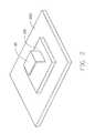
- FIG. 3is a view of a system-in-package integrated circuit according to the prior art.
- an embodiment of an integrated circuit (IC) module 100includes a carrier substrate 10 , a semiconductor die 20 mounted in the carrier substrate 10 , and an antenna 30 partially embedded in the carrier substrate 10 .
- the semiconductor die 20has a plurality of semiconductor elements integrated together for implementing major functions of the IC module 100 .
- the carrier substrate 10includes a plurality of package layers 11 , 12 , 13 , 14 . Each of the package layers 11 , 12 , 13 , 14 includes conductive traces and via-holes (not shown) that electrically connect to the semiconductor die 20 .
- the package layers 11 , 12 , 13 , 14provide electrical connections between the semiconductor die 20 and an external circuit.
- a plurality of solder balls 70is attached to a bottom surface of the carrier substrate 10 for electrically connecting the IC module 100 to a printed circuit board (PCB).
- PCBprinted circuit board
- a cavity 16is defined in a central portion of the carrier substrate 10 for receiving the semiconductor die 20 therein.
- a top surface of the semiconductor die 20lies in the same plane as that of the carrier substrate 10 .
- the IC module 100further includes a ground pad 40 disposed on the top surface of the carrier substrate 10 and the semiconductor die 20 .
- the ground pad 40provides shielding to the semiconductor die 20 from radiation emitting from the antenna 30 .
- the antenna 30includes an L-shaped main body and a ground layer 50 disposed on the ground pad 40 .
- the L-shaped main body of the antenna 30includes a support lever 32 perpendicular to the ground layer 50 and a planar portion 34 extending perpendicularly from a top edge of the support lever 32 for receiving communication signals.
- a lower end of the support lever 32 of the antenna 30extends through the ground pad 40 and extends into the carrier substrate 10 .
- the antenna 30is connected to the semiconductor die 20 via a plurality of bonding wires 60 and capable of communicating with the semiconductor die 20 .
- the antenna 30is made of heat conductive material (such as metal) and integrally formed.
- the ground layer 50 of the antenna 30can partially or fully contact the ground pad 40 for facilitating heat dissipation for the semiconductor die 20 .
- the IC module 100is attached on a circuit board 200 .
- the circuit board 200is configured to be attached in a portable electronic device (such as a cell phone).
- the antenna 30is partially extended out from the electronic device for receiving communication signals and capable of conducting the heat generated by the IC module 100 out from the electronic device, thereby preventing the semiconductor die 20 from overheating.
- the antenna 30performs two functions simultaneously.
Landscapes
- Physics & Mathematics (AREA)
- Condensed Matter Physics & Semiconductors (AREA)
- General Physics & Mathematics (AREA)
- Engineering & Computer Science (AREA)
- Computer Hardware Design (AREA)
- Microelectronics & Electronic Packaging (AREA)
- Power Engineering (AREA)
- Health & Medical Sciences (AREA)
- Electromagnetism (AREA)
- Toxicology (AREA)
- Cooling Or The Like Of Semiconductors Or Solid State Devices (AREA)
- Semiconductor Integrated Circuits (AREA)
Abstract
Description
1. Technical Field
The present disclosure relates to an integrated circuit module with an antenna.
2. Description of Related Art
In electronics, an integrated circuit (also known as IC, microcircuit, microchip, silicon chip, or chip) is a miniaturized electronic circuit (consisting mainly of semiconductor devices, as well as passive components) that has been manufactured on the surface of a thin substrate of semiconductor material. Integrated circuits are used in almost all electronic equipment in use today and have revolutionized the world of electronics.
Recently, in mobile devices, such as mobile phones and Personal Digital Assistants (PDAs), technology for System-in-Package (SiP), in which various systems and passive devices are implemented in the form of a single package to realize the small size of the mobile devices, and in which an antenna for data transmission/reception is also integrated in the package, has been widely used.
Referring toFIG. 3 , a conventional SiP integrated circuit, according to the prior art, includes anantenna 2 embedded in an integrated circuit (IC)package 1. The integrated circuit can receive or transmit communication signals via theantenna 2. However, theantenna 2 integrated in theIC package 1 may cause signal interference and heat transfer deterioration in the integrated circuit.
What is needed, therefore, is an integrated circuit module integrated with an antenna capable of decreasing signal interference and dissipating heat from the integrated circuit module.
The disclosure is illustrated by way of example and not by way of limitation in the figures of the accompanying drawings in which like references indicate similar elements. It should be noted that references to “an” or “one” embodiment in this disclosure are not necessarily to the same embodiment, and such references mean at least one.
Referring toFIG. 1 , an embodiment of an integrated circuit (IC)module 100 includes acarrier substrate 10, asemiconductor die 20 mounted in thecarrier substrate 10, and anantenna 30 partially embedded in thecarrier substrate 10. The semiconductor die20 has a plurality of semiconductor elements integrated together for implementing major functions of theIC module 100. Thecarrier substrate 10 includes a plurality ofpackage layers package layers package layers semiconductor die 20 and an external circuit. A plurality ofsolder balls 70 is attached to a bottom surface of thecarrier substrate 10 for electrically connecting theIC module 100 to a printed circuit board (PCB).
Acavity 16 is defined in a central portion of thecarrier substrate 10 for receiving the semiconductor die20 therein. A top surface of the semiconductor die20 lies in the same plane as that of thecarrier substrate 10.
TheIC module 100 further includes aground pad 40 disposed on the top surface of thecarrier substrate 10 and the semiconductor die20. Theground pad 40 provides shielding to the semiconductor die20 from radiation emitting from theantenna 30. Theantenna 30 includes an L-shaped main body and aground layer 50 disposed on theground pad 40.
The L-shaped main body of theantenna 30 includes asupport lever 32 perpendicular to theground layer 50 and aplanar portion 34 extending perpendicularly from a top edge of thesupport lever 32 for receiving communication signals. A lower end of thesupport lever 32 of theantenna 30 extends through theground pad 40 and extends into thecarrier substrate 10. Theantenna 30 is connected to the semiconductor die20 via a plurality ofbonding wires 60 and capable of communicating with the semiconductor die20.
In the embodiment, theantenna 30 is made of heat conductive material (such as metal) and integrally formed. Theground layer 50 of theantenna 30 can partially or fully contact theground pad 40 for facilitating heat dissipation for thesemiconductor die 20.
Referring toFIG. 2 , theIC module 100 is attached on acircuit board 200. Thecircuit board 200 is configured to be attached in a portable electronic device (such as a cell phone). Theantenna 30 is partially extended out from the electronic device for receiving communication signals and capable of conducting the heat generated by theIC module 100 out from the electronic device, thereby preventing the semiconductor die20 from overheating. Thus theantenna 30 performs two functions simultaneously.
While the present disclosure has been illustrated by the description of preferred embodiments thereof, and while the preferred embodiments have been described in considerable detail, it is not intended to restrict or in any way limit the scope of the appended claims to such details. Additional advantages and modifications within the spirit and scope of the present disclosure will readily appear to those skilled in the art. Therefore, the present disclosure is not limited to the specific details and illustrative examples shown and described.
Claims (15)
1. An integrated circuit module comprising:
a carrier substrate having an upper surface and a lower surface, the lower surface having a plurality of solder balls for electrically connecting to an external circuit;
a semiconductor die disposed in the carrier substrate;
a ground pad disposed on the upper surface that provides shielding to the semiconductor die; and
an antenna attached to the carrier substrate, wherein the antenna is capable of transmitting or receiving communication signals and comprises a ground layer in thermal contact with the ground pad for dissipating heat generated from the integrated circuit module.
2. The integrated circuit module ofclaim 1 , wherein the antenna further comprises an L-shaped main body that is connected to the ground layer.
3. The integrated circuit module ofclaim 2 , wherein the main body of the antenna comprises a support level that is perpendicular to the ground layer and a planar portion that extends perpendicularly from a top end of the support lever.
4. The integrated circuit module ofclaim 3 , wherein a lower end of the support lever extends through the ground pad and extends into the carrier substrate.
5. The integrated circuit module ofclaim 1 , wherein a top surface of the semiconductor die lies in the same plane as that of the carrier substrate.
6. The integrated circuit module ofclaim 1 , wherein the carrier substrate comprises a plurality of package layers that provides connections between the semiconductor die and the external circuit.
7. The integrated circuit module ofclaim 1 , wherein a cavity is defined in a central portion of the carrier substrate and receives the semiconductor die therein.
8. The integrated circuit module ofclaim 1 , wherein a lower end of the antenna is extended into the carrier substrate and connected with the semiconductor die via wire bonds.
9. An integrated circuit module comprising:
a carrier substrate with a cavity defined therein;
a semiconductor die mounted in the cavity of the carrier substrate;
a ground pad disposed on the carrier substrate and the semiconductor die; and
an antenna that is in communication with the semiconductor die, in contact with the ground pad, capable of conducting heat generated from the integrated circuit module, and extends into the carrier substrate.
10. The integrated circuit module ofclaim 9 , wherein the antenna further comprises a main body that is capable of receiving and transmitting signals, and a ground layer that is connected to the main body; the ground layer is in thermal contact with the ground pad.
11. The integrated circuit module ofclaim 10 , wherein the antenna is formed of a single piece of heat-conductive material.
12. The integrated circuit module ofclaim 10 , wherein an area of the ground layer of the antenna is same as that of the ground pad.
13. The integrated circuit module ofclaim 10 , wherein the main body of the antenna comprises a support level that is perpendicular to the ground layer and a planar portion that extends perpendicularly from a top end of the support lever.
14. The integrated circuit module ofclaim 13 , wherein a lower end of the support level extends through the ground pad and partially extended into the carrier substrate.
15. The integrated circuit module ofclaim 9 , wherein the carrier substrate comprises a plurality of package layers that provides connections between the semiconductor die and an external circuit.
Applications Claiming Priority (2)
| Application Number | Priority Date | Filing Date | Title |
|---|---|---|---|
| CN200920316151.2UCN201629397U (en) | 2009-11-30 | 2009-11-30 | IC Portfolio |
| CN200920316151.2 | 2009-11-30 |
Publications (2)
| Publication Number | Publication Date |
|---|---|
| US20110127665A1 US20110127665A1 (en) | 2011-06-02 |
| US8319298B2true US8319298B2 (en) | 2012-11-27 |
Family
ID=43060795
Family Applications (1)
| Application Number | Title | Priority Date | Filing Date |
|---|---|---|---|
| US12/701,684Expired - Fee RelatedUS8319298B2 (en) | 2009-11-30 | 2010-02-08 | Integrated circuit module |
Country Status (2)
| Country | Link |
|---|---|
| US (1) | US8319298B2 (en) |
| CN (1) | CN201629397U (en) |
Cited By (29)
| Publication number | Priority date | Publication date | Assignee | Title |
|---|---|---|---|---|
| US20140176392A1 (en)* | 2012-12-20 | 2014-06-26 | Samsung Electro-Mechanics Co., Ltd. | Antenna and front end module |
| US9064642B2 (en) | 2013-03-10 | 2015-06-23 | Apple Inc. | Rattle-free keyswitch mechanism |
| US9412533B2 (en) | 2013-05-27 | 2016-08-09 | Apple Inc. | Low travel switch assembly |
| US9449772B2 (en) | 2012-10-30 | 2016-09-20 | Apple Inc. | Low-travel key mechanisms using butterfly hinges |
| US9502193B2 (en) | 2012-10-30 | 2016-11-22 | Apple Inc. | Low-travel key mechanisms using butterfly hinges |
| US9640347B2 (en) | 2013-09-30 | 2017-05-02 | Apple Inc. | Keycaps with reduced thickness |
| US9704670B2 (en) | 2013-09-30 | 2017-07-11 | Apple Inc. | Keycaps having reduced thickness |
| US9704665B2 (en) | 2014-05-19 | 2017-07-11 | Apple Inc. | Backlit keyboard including reflective component |
| US9710069B2 (en) | 2012-10-30 | 2017-07-18 | Apple Inc. | Flexible printed circuit having flex tails upon which keyboard keycaps are coupled |
| US9715978B2 (en) | 2014-05-27 | 2017-07-25 | Apple Inc. | Low travel switch assembly |
| US9779889B2 (en) | 2014-03-24 | 2017-10-03 | Apple Inc. | Scissor mechanism features for a keyboard |
| US9793066B1 (en) | 2014-01-31 | 2017-10-17 | Apple Inc. | Keyboard hinge mechanism |
| US9870880B2 (en) | 2014-09-30 | 2018-01-16 | Apple Inc. | Dome switch and switch housing for keyboard assembly |
| US9908310B2 (en) | 2013-07-10 | 2018-03-06 | Apple Inc. | Electronic device with a reduced friction surface |
| US9927895B2 (en) | 2013-02-06 | 2018-03-27 | Apple Inc. | Input/output device with a dynamically adjustable appearance and function |
| US9934915B2 (en) | 2015-06-10 | 2018-04-03 | Apple Inc. | Reduced layer keyboard stack-up |
| US9971084B2 (en) | 2015-09-28 | 2018-05-15 | Apple Inc. | Illumination structure for uniform illumination of keys |
| US9997308B2 (en) | 2015-05-13 | 2018-06-12 | Apple Inc. | Low-travel key mechanism for an input device |
| US9997304B2 (en) | 2015-05-13 | 2018-06-12 | Apple Inc. | Uniform illumination of keys |
| US10083805B2 (en) | 2015-05-13 | 2018-09-25 | Apple Inc. | Keyboard for electronic device |
| US10082880B1 (en) | 2014-08-28 | 2018-09-25 | Apple Inc. | System level features of a keyboard |
| US10115544B2 (en) | 2016-08-08 | 2018-10-30 | Apple Inc. | Singulated keyboard assemblies and methods for assembling a keyboard |
| US10128064B2 (en) | 2015-05-13 | 2018-11-13 | Apple Inc. | Keyboard assemblies having reduced thicknesses and method of forming keyboard assemblies |
| US10211514B2 (en) | 2014-05-28 | 2019-02-19 | Samsung Electronics Co., Ltd. | Antenna using conductor and electronic device therefor |
| US10353485B1 (en) | 2016-07-27 | 2019-07-16 | Apple Inc. | Multifunction input device with an embedded capacitive sensing layer |
| US10755877B1 (en) | 2016-08-29 | 2020-08-25 | Apple Inc. | Keyboard for an electronic device |
| US10775850B2 (en) | 2017-07-26 | 2020-09-15 | Apple Inc. | Computer with keyboard |
| US10796863B2 (en) | 2014-08-15 | 2020-10-06 | Apple Inc. | Fabric keyboard |
| US11500538B2 (en) | 2016-09-13 | 2022-11-15 | Apple Inc. | Keyless keyboard with force sensing and haptic feedback |
Families Citing this family (2)
| Publication number | Priority date | Publication date | Assignee | Title |
|---|---|---|---|---|
| US9966653B2 (en) | 2015-08-28 | 2018-05-08 | Apple Inc. | Antennas for electronic device with heat spreader |
| US10593635B2 (en) | 2018-03-27 | 2020-03-17 | Nxp B.V. | Multi-die and antenna array device |
Citations (12)
| Publication number | Priority date | Publication date | Assignee | Title |
|---|---|---|---|---|
| US20040099940A1 (en)* | 2002-11-22 | 2004-05-27 | International Rectifier Corporation | Semiconductor device having clips for connecting to external elements |
| US6770955B1 (en)* | 2001-12-15 | 2004-08-03 | Skyworks Solutions, Inc. | Shielded antenna in a semiconductor package |
| US20050093145A1 (en)* | 2003-11-05 | 2005-05-05 | Interdigital Technology Corporation | Asic-embedded switchable antenna arrays |
| US6946726B1 (en)* | 2003-11-26 | 2005-09-20 | Actel Corporation | Chip carrier substrate with a land grid array and external bond terminals |
| US20070122960A1 (en)* | 2005-11-29 | 2007-05-31 | Semiconductor Energy Laboratory Co., Ltd. | Antenna and manufacturing method thereof, semiconductor device including antenna and manufacturing method thereof, and radio communication system |
| US20070200146A1 (en)* | 2006-02-28 | 2007-08-30 | Keiji Onishi | Electronic device, method for producing the same, and communication apparatus including the same |
| US20080217760A1 (en)* | 2007-03-08 | 2008-09-11 | Fuji Electric Device Technology Co., Ltd. | Semiconductor device and method of manufacturing same |
| US7470977B2 (en)* | 2002-07-03 | 2008-12-30 | Sony Corporation | Modular board device, high frequency module, and method of manufacturing same |
| US20090091018A1 (en)* | 2005-11-16 | 2009-04-09 | Kyocera Corporation | Electronic Component Sealing Substrate, Electronic Component Sealing Substrate to be Divided Into a Plurality of Pieces, Electronic Apparatus Including Electronic Component Sealing Substrate, and Method for Producing Electronic Apparatus |
| US20110062549A1 (en)* | 2009-09-11 | 2011-03-17 | Stats Chippac, Ltd. | Semiconductor Device and Method of Forming Integrated Passive Device |
| US20110068433A1 (en)* | 2009-09-24 | 2011-03-24 | Qualcomm Incorporated | Forming radio frequency integrated circuits |
| US8232621B2 (en)* | 2006-07-28 | 2012-07-31 | Semiconductor Energy Laboratory Co., Ltd. | Semiconductor device |
- 2009
- 2009-11-30CNCN200920316151.2Upatent/CN201629397U/ennot_activeExpired - Fee Related
- 2010
- 2010-02-08USUS12/701,684patent/US8319298B2/ennot_activeExpired - Fee Related
Patent Citations (13)
| Publication number | Priority date | Publication date | Assignee | Title |
|---|---|---|---|---|
| US6770955B1 (en)* | 2001-12-15 | 2004-08-03 | Skyworks Solutions, Inc. | Shielded antenna in a semiconductor package |
| US7470977B2 (en)* | 2002-07-03 | 2008-12-30 | Sony Corporation | Modular board device, high frequency module, and method of manufacturing same |
| US20040099940A1 (en)* | 2002-11-22 | 2004-05-27 | International Rectifier Corporation | Semiconductor device having clips for connecting to external elements |
| US20050093145A1 (en)* | 2003-11-05 | 2005-05-05 | Interdigital Technology Corporation | Asic-embedded switchable antenna arrays |
| US20070228548A1 (en)* | 2003-11-26 | 2007-10-04 | Actel Corporation | Chip carrier substrate with a land grid array and external bond terminals |
| US6946726B1 (en)* | 2003-11-26 | 2005-09-20 | Actel Corporation | Chip carrier substrate with a land grid array and external bond terminals |
| US20090091018A1 (en)* | 2005-11-16 | 2009-04-09 | Kyocera Corporation | Electronic Component Sealing Substrate, Electronic Component Sealing Substrate to be Divided Into a Plurality of Pieces, Electronic Apparatus Including Electronic Component Sealing Substrate, and Method for Producing Electronic Apparatus |
| US20070122960A1 (en)* | 2005-11-29 | 2007-05-31 | Semiconductor Energy Laboratory Co., Ltd. | Antenna and manufacturing method thereof, semiconductor device including antenna and manufacturing method thereof, and radio communication system |
| US20070200146A1 (en)* | 2006-02-28 | 2007-08-30 | Keiji Onishi | Electronic device, method for producing the same, and communication apparatus including the same |
| US8232621B2 (en)* | 2006-07-28 | 2012-07-31 | Semiconductor Energy Laboratory Co., Ltd. | Semiconductor device |
| US20080217760A1 (en)* | 2007-03-08 | 2008-09-11 | Fuji Electric Device Technology Co., Ltd. | Semiconductor device and method of manufacturing same |
| US20110062549A1 (en)* | 2009-09-11 | 2011-03-17 | Stats Chippac, Ltd. | Semiconductor Device and Method of Forming Integrated Passive Device |
| US20110068433A1 (en)* | 2009-09-24 | 2011-03-24 | Qualcomm Incorporated | Forming radio frequency integrated circuits |
Non-Patent Citations (1)
| Title |
|---|
| Rogier, H "Design of an on-package slot antenna for bluetooth applications" Conf. on Elec. Perf. of Elec. Pack. 2000 IEEE Oct. 25, 2000 pp. 292-295.* |
Cited By (55)
| Publication number | Priority date | Publication date | Assignee | Title |
|---|---|---|---|---|
| US9761389B2 (en) | 2012-10-30 | 2017-09-12 | Apple Inc. | Low-travel key mechanisms with butterfly hinges |
| US9916945B2 (en) | 2012-10-30 | 2018-03-13 | Apple Inc. | Low-travel key mechanisms using butterfly hinges |
| US10699856B2 (en) | 2012-10-30 | 2020-06-30 | Apple Inc. | Low-travel key mechanisms using butterfly hinges |
| US9449772B2 (en) | 2012-10-30 | 2016-09-20 | Apple Inc. | Low-travel key mechanisms using butterfly hinges |
| US9502193B2 (en) | 2012-10-30 | 2016-11-22 | Apple Inc. | Low-travel key mechanisms using butterfly hinges |
| US10211008B2 (en) | 2012-10-30 | 2019-02-19 | Apple Inc. | Low-travel key mechanisms using butterfly hinges |
| US10254851B2 (en) | 2012-10-30 | 2019-04-09 | Apple Inc. | Keyboard key employing a capacitive sensor and dome |
| US11023081B2 (en) | 2012-10-30 | 2021-06-01 | Apple Inc. | Multi-functional keyboard assemblies |
| US9710069B2 (en) | 2012-10-30 | 2017-07-18 | Apple Inc. | Flexible printed circuit having flex tails upon which keyboard keycaps are coupled |
| US9246209B2 (en)* | 2012-12-20 | 2016-01-26 | Samsung Electro-Mechanics Co., Ltd. | Antenna and front end module |
| US20140176392A1 (en)* | 2012-12-20 | 2014-06-26 | Samsung Electro-Mechanics Co., Ltd. | Antenna and front end module |
| US10114489B2 (en) | 2013-02-06 | 2018-10-30 | Apple Inc. | Input/output device with a dynamically adjustable appearance and function |
| US9927895B2 (en) | 2013-02-06 | 2018-03-27 | Apple Inc. | Input/output device with a dynamically adjustable appearance and function |
| US9064642B2 (en) | 2013-03-10 | 2015-06-23 | Apple Inc. | Rattle-free keyswitch mechanism |
| US10262814B2 (en) | 2013-05-27 | 2019-04-16 | Apple Inc. | Low travel switch assembly |
| US9412533B2 (en) | 2013-05-27 | 2016-08-09 | Apple Inc. | Low travel switch assembly |
| US10556408B2 (en) | 2013-07-10 | 2020-02-11 | Apple Inc. | Electronic device with a reduced friction surface |
| US9908310B2 (en) | 2013-07-10 | 2018-03-06 | Apple Inc. | Electronic device with a reduced friction surface |
| US9704670B2 (en) | 2013-09-30 | 2017-07-11 | Apple Inc. | Keycaps having reduced thickness |
| US10804051B2 (en) | 2013-09-30 | 2020-10-13 | Apple Inc. | Keycaps having reduced thickness |
| US11699558B2 (en) | 2013-09-30 | 2023-07-11 | Apple Inc. | Keycaps having reduced thickness |
| US10002727B2 (en) | 2013-09-30 | 2018-06-19 | Apple Inc. | Keycaps with reduced thickness |
| US10224157B2 (en) | 2013-09-30 | 2019-03-05 | Apple Inc. | Keycaps having reduced thickness |
| US9640347B2 (en) | 2013-09-30 | 2017-05-02 | Apple Inc. | Keycaps with reduced thickness |
| US9793066B1 (en) | 2014-01-31 | 2017-10-17 | Apple Inc. | Keyboard hinge mechanism |
| US9779889B2 (en) | 2014-03-24 | 2017-10-03 | Apple Inc. | Scissor mechanism features for a keyboard |
| US9704665B2 (en) | 2014-05-19 | 2017-07-11 | Apple Inc. | Backlit keyboard including reflective component |
| US9715978B2 (en) | 2014-05-27 | 2017-07-25 | Apple Inc. | Low travel switch assembly |
| US10211514B2 (en) | 2014-05-28 | 2019-02-19 | Samsung Electronics Co., Ltd. | Antenna using conductor and electronic device therefor |
| US10796863B2 (en) | 2014-08-15 | 2020-10-06 | Apple Inc. | Fabric keyboard |
| US10082880B1 (en) | 2014-08-28 | 2018-09-25 | Apple Inc. | System level features of a keyboard |
| US10192696B2 (en) | 2014-09-30 | 2019-01-29 | Apple Inc. | Light-emitting assembly for keyboard |
| US10134539B2 (en) | 2014-09-30 | 2018-11-20 | Apple Inc. | Venting system and shield for keyboard |
| US10879019B2 (en) | 2014-09-30 | 2020-12-29 | Apple Inc. | Light-emitting assembly for keyboard |
| US10128061B2 (en) | 2014-09-30 | 2018-11-13 | Apple Inc. | Key and switch housing for keyboard assembly |
| US9870880B2 (en) | 2014-09-30 | 2018-01-16 | Apple Inc. | Dome switch and switch housing for keyboard assembly |
| US10468211B2 (en) | 2015-05-13 | 2019-11-05 | Apple Inc. | Illuminated low-travel key mechanism for a keyboard |
| US10083806B2 (en) | 2015-05-13 | 2018-09-25 | Apple Inc. | Keyboard for electronic device |
| US10424446B2 (en) | 2015-05-13 | 2019-09-24 | Apple Inc. | Keyboard assemblies having reduced thickness and method of forming keyboard assemblies |
| US10083805B2 (en) | 2015-05-13 | 2018-09-25 | Apple Inc. | Keyboard for electronic device |
| US9997304B2 (en) | 2015-05-13 | 2018-06-12 | Apple Inc. | Uniform illumination of keys |
| US10128064B2 (en) | 2015-05-13 | 2018-11-13 | Apple Inc. | Keyboard assemblies having reduced thicknesses and method of forming keyboard assemblies |
| US9997308B2 (en) | 2015-05-13 | 2018-06-12 | Apple Inc. | Low-travel key mechanism for an input device |
| US9934915B2 (en) | 2015-06-10 | 2018-04-03 | Apple Inc. | Reduced layer keyboard stack-up |
| US10310167B2 (en) | 2015-09-28 | 2019-06-04 | Apple Inc. | Illumination structure for uniform illumination of keys |
| US9971084B2 (en) | 2015-09-28 | 2018-05-15 | Apple Inc. | Illumination structure for uniform illumination of keys |
| US10353485B1 (en) | 2016-07-27 | 2019-07-16 | Apple Inc. | Multifunction input device with an embedded capacitive sensing layer |
| US11282659B2 (en) | 2016-08-08 | 2022-03-22 | Apple Inc. | Singulated keyboard assemblies and methods for assembling a keyboard |
| US10115544B2 (en) | 2016-08-08 | 2018-10-30 | Apple Inc. | Singulated keyboard assemblies and methods for assembling a keyboard |
| US10755877B1 (en) | 2016-08-29 | 2020-08-25 | Apple Inc. | Keyboard for an electronic device |
| US11500538B2 (en) | 2016-09-13 | 2022-11-15 | Apple Inc. | Keyless keyboard with force sensing and haptic feedback |
| US10775850B2 (en) | 2017-07-26 | 2020-09-15 | Apple Inc. | Computer with keyboard |
| US11409332B2 (en) | 2017-07-26 | 2022-08-09 | Apple Inc. | Computer with keyboard |
| US11619976B2 (en) | 2017-07-26 | 2023-04-04 | Apple Inc. | Computer with keyboard |
| US12079043B2 (en) | 2017-07-26 | 2024-09-03 | Apple Inc. | Computer with keyboard |
Also Published As
| Publication number | Publication date |
|---|---|
| CN201629397U (en) | 2010-11-10 |
| US20110127665A1 (en) | 2011-06-02 |
Similar Documents
| Publication | Publication Date | Title |
|---|---|---|
| US8319298B2 (en) | Integrated circuit module | |
| EP1737068B1 (en) | Wireless local area network communications module and integrated chip package | |
| EP2626897B1 (en) | Transmission line transition having vertical structure and single chip package using land grid array joining | |
| US20150115467A1 (en) | Package-on-package device | |
| US10861812B2 (en) | Electronic apparatus | |
| CN102573279A (en) | Semiconductor package and method of forming the same | |
| US20080084677A1 (en) | Electronic apparatus | |
| CN112018101A (en) | Semiconductor packaging | |
| CN105762138A (en) | Integrated millimeter wave chip packaging structure | |
| KR20100010747A (en) | Semiconductor device package | |
| KR20050002659A (en) | Hybrid integrated circuit | |
| JP4284744B2 (en) | High frequency integrated circuit device | |
| JP2006120996A (en) | Circuit module | |
| KR20150076816A (en) | Electronic device module | |
| US11682660B2 (en) | Semiconductor structure | |
| US7352056B2 (en) | Semiconductor package structure with microstrip antennan | |
| US11791251B2 (en) | High power laminate RF package | |
| US8581394B2 (en) | Semiconductor package module and electric circuit assembly with the same | |
| KR20090129208A (en) | Semiconductor device and manufacturing method thereof | |
| TWM381844U (en) | Integrated circuit assembly | |
| KR20060020483A (en) | PCB | |
| KR20100023226A (en) | Multi-chip module package | |
| KR20100002723A (en) | Semiconductor package and method for manufacturing the semiconductor package |
Legal Events
| Date | Code | Title | Description |
|---|---|---|---|
| AS | Assignment | Owner name:HON HAI PRECISION INDUSTRY CO., LTD., TAIWAN Free format text:ASSIGNMENT OF ASSIGNORS INTEREST;ASSIGNOR:HSU, HSIUAN-JU;REEL/FRAME:023909/0478 Effective date:20100204 | |
| CC | Certificate of correction | ||
| REMI | Maintenance fee reminder mailed | ||
| LAPS | Lapse for failure to pay maintenance fees | ||
| STCH | Information on status: patent discontinuation | Free format text:PATENT EXPIRED DUE TO NONPAYMENT OF MAINTENANCE FEES UNDER 37 CFR 1.362 | |
| FP | Lapsed due to failure to pay maintenance fee | Effective date:20161127 |