US8316536B1 - Multi-level circuit substrate fabrication method - Google Patents
Multi-level circuit substrate fabrication methodDownload PDFInfo
- Publication number
- US8316536B1 US8316536B1US12/151,857US15185708AUS8316536B1US 8316536 B1US8316536 B1US 8316536B1US 15185708 AUS15185708 AUS 15185708AUS 8316536 B1US8316536 B1US 8316536B1
- Authority
- US
- United States
- Prior art keywords
- dielectric layer
- metal circuit
- plane
- level metal
- features
- Prior art date
- Legal status (The legal status is an assumption and is not a legal conclusion. Google has not performed a legal analysis and makes no representation as to the accuracy of the status listed.)
- Expired - Fee Related, expires
Links
Images


Classifications
- H—ELECTRICITY
- H01—ELECTRIC ELEMENTS
- H01L—SEMICONDUCTOR DEVICES NOT COVERED BY CLASS H10
- H01L24/00—Arrangements for connecting or disconnecting semiconductor or solid-state bodies; Methods or apparatus related thereto
- H01L24/73—Means for bonding being of different types provided for in two or more of groups H01L24/10, H01L24/18, H01L24/26, H01L24/34, H01L24/42, H01L24/50, H01L24/63, H01L24/71
- H—ELECTRICITY
- H01—ELECTRIC ELEMENTS
- H01L—SEMICONDUCTOR DEVICES NOT COVERED BY CLASS H10
- H01L21/00—Processes or apparatus adapted for the manufacture or treatment of semiconductor or solid state devices or of parts thereof
- H01L21/02—Manufacture or treatment of semiconductor devices or of parts thereof
- H01L21/04—Manufacture or treatment of semiconductor devices or of parts thereof the devices having potential barriers, e.g. a PN junction, depletion layer or carrier concentration layer
- H01L21/48—Manufacture or treatment of parts, e.g. containers, prior to assembly of the devices, using processes not provided for in a single one of the groups H01L21/18 - H01L21/326 or H10D48/04 - H10D48/07
- H01L21/4814—Conductive parts
- H01L21/4846—Leads on or in insulating or insulated substrates, e.g. metallisation
- H01L21/4857—Multilayer substrates
- H—ELECTRICITY
- H05—ELECTRIC TECHNIQUES NOT OTHERWISE PROVIDED FOR
- H05K—PRINTED CIRCUITS; CASINGS OR CONSTRUCTIONAL DETAILS OF ELECTRIC APPARATUS; MANUFACTURE OF ASSEMBLAGES OF ELECTRICAL COMPONENTS
- H05K3/00—Apparatus or processes for manufacturing printed circuits
- H05K3/10—Apparatus or processes for manufacturing printed circuits in which conductive material is applied to the insulating support in such a manner as to form the desired conductive pattern
- H05K3/107—Apparatus or processes for manufacturing printed circuits in which conductive material is applied to the insulating support in such a manner as to form the desired conductive pattern by filling grooves in the support with conductive material
- H—ELECTRICITY
- H05—ELECTRIC TECHNIQUES NOT OTHERWISE PROVIDED FOR
- H05K—PRINTED CIRCUITS; CASINGS OR CONSTRUCTIONAL DETAILS OF ELECTRIC APPARATUS; MANUFACTURE OF ASSEMBLAGES OF ELECTRICAL COMPONENTS
- H05K3/00—Apparatus or processes for manufacturing printed circuits
- H05K3/10—Apparatus or processes for manufacturing printed circuits in which conductive material is applied to the insulating support in such a manner as to form the desired conductive pattern
- H05K3/12—Apparatus or processes for manufacturing printed circuits in which conductive material is applied to the insulating support in such a manner as to form the desired conductive pattern using thick film techniques, e.g. printing techniques to apply the conductive material or similar techniques for applying conductive paste or ink patterns
- H05K3/1258—Apparatus or processes for manufacturing printed circuits in which conductive material is applied to the insulating support in such a manner as to form the desired conductive pattern using thick film techniques, e.g. printing techniques to apply the conductive material or similar techniques for applying conductive paste or ink patterns by using a substrate provided with a shape pattern, e.g. grooves, banks, resist pattern
- H—ELECTRICITY
- H05—ELECTRIC TECHNIQUES NOT OTHERWISE PROVIDED FOR
- H05K—PRINTED CIRCUITS; CASINGS OR CONSTRUCTIONAL DETAILS OF ELECTRIC APPARATUS; MANUFACTURE OF ASSEMBLAGES OF ELECTRICAL COMPONENTS
- H05K7/00—Constructional details common to different types of electric apparatus
- H05K7/02—Arrangements of circuit components or wiring on supporting structure
- H05K7/10—Plug-in assemblages of components, e.g. IC sockets
- H05K7/1053—Plug-in assemblages of components, e.g. IC sockets having interior leads
- H05K7/1061—Plug-in assemblages of components, e.g. IC sockets having interior leads co-operating by abutting
- H—ELECTRICITY
- H01—ELECTRIC ELEMENTS
- H01L—SEMICONDUCTOR DEVICES NOT COVERED BY CLASS H10
- H01L2224/00—Indexing scheme for arrangements for connecting or disconnecting semiconductor or solid-state bodies and methods related thereto as covered by H01L24/00
- H01L2224/01—Means for bonding being attached to, or being formed on, the surface to be connected, e.g. chip-to-package, die-attach, "first-level" interconnects; Manufacturing methods related thereto
- H01L2224/10—Bump connectors; Manufacturing methods related thereto
- H01L2224/15—Structure, shape, material or disposition of the bump connectors after the connecting process
- H01L2224/16—Structure, shape, material or disposition of the bump connectors after the connecting process of an individual bump connector
- H—ELECTRICITY
- H01—ELECTRIC ELEMENTS
- H01L—SEMICONDUCTOR DEVICES NOT COVERED BY CLASS H10
- H01L2224/00—Indexing scheme for arrangements for connecting or disconnecting semiconductor or solid-state bodies and methods related thereto as covered by H01L24/00
- H01L2224/01—Means for bonding being attached to, or being formed on, the surface to be connected, e.g. chip-to-package, die-attach, "first-level" interconnects; Manufacturing methods related thereto
- H01L2224/26—Layer connectors, e.g. plate connectors, solder or adhesive layers; Manufacturing methods related thereto
- H01L2224/31—Structure, shape, material or disposition of the layer connectors after the connecting process
- H01L2224/32—Structure, shape, material or disposition of the layer connectors after the connecting process of an individual layer connector
- H01L2224/321—Disposition
- H01L2224/32151—Disposition the layer connector connecting between a semiconductor or solid-state body and an item not being a semiconductor or solid-state body, e.g. chip-to-substrate, chip-to-passive
- H01L2224/32221—Disposition the layer connector connecting between a semiconductor or solid-state body and an item not being a semiconductor or solid-state body, e.g. chip-to-substrate, chip-to-passive the body and the item being stacked
- H01L2224/32225—Disposition the layer connector connecting between a semiconductor or solid-state body and an item not being a semiconductor or solid-state body, e.g. chip-to-substrate, chip-to-passive the body and the item being stacked the item being non-metallic, e.g. insulating substrate with or without metallisation
- H—ELECTRICITY
- H01—ELECTRIC ELEMENTS
- H01L—SEMICONDUCTOR DEVICES NOT COVERED BY CLASS H10
- H01L2224/00—Indexing scheme for arrangements for connecting or disconnecting semiconductor or solid-state bodies and methods related thereto as covered by H01L24/00
- H01L2224/01—Means for bonding being attached to, or being formed on, the surface to be connected, e.g. chip-to-package, die-attach, "first-level" interconnects; Manufacturing methods related thereto
- H01L2224/42—Wire connectors; Manufacturing methods related thereto
- H01L2224/47—Structure, shape, material or disposition of the wire connectors after the connecting process
- H01L2224/48—Structure, shape, material or disposition of the wire connectors after the connecting process of an individual wire connector
- H01L2224/4805—Shape
- H01L2224/4809—Loop shape
- H01L2224/48091—Arched
- H—ELECTRICITY
- H01—ELECTRIC ELEMENTS
- H01L—SEMICONDUCTOR DEVICES NOT COVERED BY CLASS H10
- H01L2224/00—Indexing scheme for arrangements for connecting or disconnecting semiconductor or solid-state bodies and methods related thereto as covered by H01L24/00
- H01L2224/01—Means for bonding being attached to, or being formed on, the surface to be connected, e.g. chip-to-package, die-attach, "first-level" interconnects; Manufacturing methods related thereto
- H01L2224/42—Wire connectors; Manufacturing methods related thereto
- H01L2224/47—Structure, shape, material or disposition of the wire connectors after the connecting process
- H01L2224/48—Structure, shape, material or disposition of the wire connectors after the connecting process of an individual wire connector
- H01L2224/481—Disposition
- H01L2224/48151—Connecting between a semiconductor or solid-state body and an item not being a semiconductor or solid-state body, e.g. chip-to-substrate, chip-to-passive
- H01L2224/48221—Connecting between a semiconductor or solid-state body and an item not being a semiconductor or solid-state body, e.g. chip-to-substrate, chip-to-passive the body and the item being stacked
- H01L2224/48225—Connecting between a semiconductor or solid-state body and an item not being a semiconductor or solid-state body, e.g. chip-to-substrate, chip-to-passive the body and the item being stacked the item being non-metallic, e.g. insulating substrate with or without metallisation
- H01L2224/48227—Connecting between a semiconductor or solid-state body and an item not being a semiconductor or solid-state body, e.g. chip-to-substrate, chip-to-passive the body and the item being stacked the item being non-metallic, e.g. insulating substrate with or without metallisation connecting the wire to a bond pad of the item
- H—ELECTRICITY
- H01—ELECTRIC ELEMENTS
- H01L—SEMICONDUCTOR DEVICES NOT COVERED BY CLASS H10
- H01L2224/00—Indexing scheme for arrangements for connecting or disconnecting semiconductor or solid-state bodies and methods related thereto as covered by H01L24/00
- H01L2224/73—Means for bonding being of different types provided for in two or more of groups H01L2224/10, H01L2224/18, H01L2224/26, H01L2224/34, H01L2224/42, H01L2224/50, H01L2224/63, H01L2224/71
- H01L2224/732—Location after the connecting process
- H01L2224/73251—Location after the connecting process on different surfaces
- H01L2224/73265—Layer and wire connectors
- H—ELECTRICITY
- H01—ELECTRIC ELEMENTS
- H01L—SEMICONDUCTOR DEVICES NOT COVERED BY CLASS H10
- H01L2924/00—Indexing scheme for arrangements or methods for connecting or disconnecting semiconductor or solid-state bodies as covered by H01L24/00
- H01L2924/01—Chemical elements
- H01L2924/01005—Boron [B]
- H—ELECTRICITY
- H01—ELECTRIC ELEMENTS
- H01L—SEMICONDUCTOR DEVICES NOT COVERED BY CLASS H10
- H01L2924/00—Indexing scheme for arrangements or methods for connecting or disconnecting semiconductor or solid-state bodies as covered by H01L24/00
- H01L2924/01—Chemical elements
- H01L2924/01006—Carbon [C]
- H—ELECTRICITY
- H01—ELECTRIC ELEMENTS
- H01L—SEMICONDUCTOR DEVICES NOT COVERED BY CLASS H10
- H01L2924/00—Indexing scheme for arrangements or methods for connecting or disconnecting semiconductor or solid-state bodies as covered by H01L24/00
- H01L2924/01—Chemical elements
- H01L2924/01029—Copper [Cu]
- H—ELECTRICITY
- H01—ELECTRIC ELEMENTS
- H01L—SEMICONDUCTOR DEVICES NOT COVERED BY CLASS H10
- H01L2924/00—Indexing scheme for arrangements or methods for connecting or disconnecting semiconductor or solid-state bodies as covered by H01L24/00
- H01L2924/01—Chemical elements
- H01L2924/01033—Arsenic [As]
- H—ELECTRICITY
- H01—ELECTRIC ELEMENTS
- H01L—SEMICONDUCTOR DEVICES NOT COVERED BY CLASS H10
- H01L2924/00—Indexing scheme for arrangements or methods for connecting or disconnecting semiconductor or solid-state bodies as covered by H01L24/00
- H01L2924/01—Chemical elements
- H01L2924/01047—Silver [Ag]
- H—ELECTRICITY
- H01—ELECTRIC ELEMENTS
- H01L—SEMICONDUCTOR DEVICES NOT COVERED BY CLASS H10
- H01L2924/00—Indexing scheme for arrangements or methods for connecting or disconnecting semiconductor or solid-state bodies as covered by H01L24/00
- H01L2924/01—Chemical elements
- H01L2924/01078—Platinum [Pt]
- H—ELECTRICITY
- H01—ELECTRIC ELEMENTS
- H01L—SEMICONDUCTOR DEVICES NOT COVERED BY CLASS H10
- H01L2924/00—Indexing scheme for arrangements or methods for connecting or disconnecting semiconductor or solid-state bodies as covered by H01L24/00
- H01L2924/01—Chemical elements
- H01L2924/01079—Gold [Au]
- H—ELECTRICITY
- H01—ELECTRIC ELEMENTS
- H01L—SEMICONDUCTOR DEVICES NOT COVERED BY CLASS H10
- H01L2924/00—Indexing scheme for arrangements or methods for connecting or disconnecting semiconductor or solid-state bodies as covered by H01L24/00
- H01L2924/01—Chemical elements
- H01L2924/01082—Lead [Pb]
- H—ELECTRICITY
- H01—ELECTRIC ELEMENTS
- H01L—SEMICONDUCTOR DEVICES NOT COVERED BY CLASS H10
- H01L2924/00—Indexing scheme for arrangements or methods for connecting or disconnecting semiconductor or solid-state bodies as covered by H01L24/00
- H01L2924/013—Alloys
- H01L2924/014—Solder alloys
- H—ELECTRICITY
- H01—ELECTRIC ELEMENTS
- H01L—SEMICONDUCTOR DEVICES NOT COVERED BY CLASS H10
- H01L2924/00—Indexing scheme for arrangements or methods for connecting or disconnecting semiconductor or solid-state bodies as covered by H01L24/00
- H01L2924/10—Details of semiconductor or other solid state devices to be connected
- H01L2924/11—Device type
- H01L2924/14—Integrated circuits
- H—ELECTRICITY
- H01—ELECTRIC ELEMENTS
- H01L—SEMICONDUCTOR DEVICES NOT COVERED BY CLASS H10
- H01L2924/00—Indexing scheme for arrangements or methods for connecting or disconnecting semiconductor or solid-state bodies as covered by H01L24/00
- H01L2924/15—Details of package parts other than the semiconductor or other solid state devices to be connected
- H01L2924/151—Die mounting substrate
- H01L2924/153—Connection portion
- H01L2924/1531—Connection portion the connection portion being formed only on the surface of the substrate opposite to the die mounting surface
- H01L2924/15311—Connection portion the connection portion being formed only on the surface of the substrate opposite to the die mounting surface being a ball array, e.g. BGA
- H—ELECTRICITY
- H01—ELECTRIC ELEMENTS
- H01L—SEMICONDUCTOR DEVICES NOT COVERED BY CLASS H10
- H01L2924/00—Indexing scheme for arrangements or methods for connecting or disconnecting semiconductor or solid-state bodies as covered by H01L24/00
- H01L2924/15—Details of package parts other than the semiconductor or other solid state devices to be connected
- H01L2924/151—Die mounting substrate
- H01L2924/156—Material
- H01L2924/157—Material with a principal constituent of the material being a metal or a metalloid, e.g. boron [B], silicon [Si], germanium [Ge], arsenic [As], antimony [Sb], tellurium [Te] and polonium [Po], and alloys thereof
- H01L2924/15738—Material with a principal constituent of the material being a metal or a metalloid, e.g. boron [B], silicon [Si], germanium [Ge], arsenic [As], antimony [Sb], tellurium [Te] and polonium [Po], and alloys thereof the principal constituent melting at a temperature of greater than or equal to 950 C and less than 1550 C
- H01L2924/15747—Copper [Cu] as principal constituent
- H—ELECTRICITY
- H01—ELECTRIC ELEMENTS
- H01L—SEMICONDUCTOR DEVICES NOT COVERED BY CLASS H10
- H01L2924/00—Indexing scheme for arrangements or methods for connecting or disconnecting semiconductor or solid-state bodies as covered by H01L24/00
- H01L2924/15—Details of package parts other than the semiconductor or other solid state devices to be connected
- H01L2924/181—Encapsulation
- H01L2924/1815—Shape
- H—ELECTRICITY
- H05—ELECTRIC TECHNIQUES NOT OTHERWISE PROVIDED FOR
- H05K—PRINTED CIRCUITS; CASINGS OR CONSTRUCTIONAL DETAILS OF ELECTRIC APPARATUS; MANUFACTURE OF ASSEMBLAGES OF ELECTRICAL COMPONENTS
- H05K1/00—Printed circuits
- H05K1/02—Details
- H05K1/03—Use of materials for the substrate
- H05K1/05—Insulated conductive substrates, e.g. insulated metal substrate
- H05K1/056—Insulated conductive substrates, e.g. insulated metal substrate the metal substrate being covered by an organic insulating layer
- H—ELECTRICITY
- H05—ELECTRIC TECHNIQUES NOT OTHERWISE PROVIDED FOR
- H05K—PRINTED CIRCUITS; CASINGS OR CONSTRUCTIONAL DETAILS OF ELECTRIC APPARATUS; MANUFACTURE OF ASSEMBLAGES OF ELECTRICAL COMPONENTS
- H05K2201/00—Indexing scheme relating to printed circuits covered by H05K1/00
- H05K2201/09—Shape and layout
- H05K2201/09009—Substrate related
- H05K2201/09036—Recesses or grooves in insulating substrate
- H—ELECTRICITY
- H05—ELECTRIC TECHNIQUES NOT OTHERWISE PROVIDED FOR
- H05K—PRINTED CIRCUITS; CASINGS OR CONSTRUCTIONAL DETAILS OF ELECTRIC APPARATUS; MANUFACTURE OF ASSEMBLAGES OF ELECTRICAL COMPONENTS
- H05K2201/00—Indexing scheme relating to printed circuits covered by H05K1/00
- H05K2201/09—Shape and layout
- H05K2201/09209—Shape and layout details of conductors
- H05K2201/095—Conductive through-holes or vias
- H05K2201/09554—Via connected to metal substrate
- H—ELECTRICITY
- H05—ELECTRIC TECHNIQUES NOT OTHERWISE PROVIDED FOR
- H05K—PRINTED CIRCUITS; CASINGS OR CONSTRUCTIONAL DETAILS OF ELECTRIC APPARATUS; MANUFACTURE OF ASSEMBLAGES OF ELECTRICAL COMPONENTS
- H05K2203/00—Indexing scheme relating to apparatus or processes for manufacturing printed circuits covered by H05K3/00
- H05K2203/07—Treatments involving liquids, e.g. plating, rinsing
- H05K2203/0703—Plating
- H05K2203/0723—Electroplating, e.g. finish plating
- H—ELECTRICITY
- H05—ELECTRIC TECHNIQUES NOT OTHERWISE PROVIDED FOR
- H05K—PRINTED CIRCUITS; CASINGS OR CONSTRUCTIONAL DETAILS OF ELECTRIC APPARATUS; MANUFACTURE OF ASSEMBLAGES OF ELECTRICAL COMPONENTS
- H05K3/00—Apparatus or processes for manufacturing printed circuits
- H05K3/0011—Working of insulating substrates or insulating layers
- H05K3/0017—Etching of the substrate by chemical or physical means
- H05K3/0026—Etching of the substrate by chemical or physical means by laser ablation
- H05K3/0032—Etching of the substrate by chemical or physical means by laser ablation of organic insulating material
- H05K3/0035—Etching of the substrate by chemical or physical means by laser ablation of organic insulating material of blind holes, i.e. having a metal layer at the bottom
- H—ELECTRICITY
- H05—ELECTRIC TECHNIQUES NOT OTHERWISE PROVIDED FOR
- H05K—PRINTED CIRCUITS; CASINGS OR CONSTRUCTIONAL DETAILS OF ELECTRIC APPARATUS; MANUFACTURE OF ASSEMBLAGES OF ELECTRICAL COMPONENTS
- H05K3/00—Apparatus or processes for manufacturing printed circuits
- H05K3/40—Forming printed elements for providing electric connections to or between printed circuits
- H05K3/42—Plated through-holes or plated via connections
- H05K3/423—Plated through-holes or plated via connections characterised by electroplating method
- Y—GENERAL TAGGING OF NEW TECHNOLOGICAL DEVELOPMENTS; GENERAL TAGGING OF CROSS-SECTIONAL TECHNOLOGIES SPANNING OVER SEVERAL SECTIONS OF THE IPC; TECHNICAL SUBJECTS COVERED BY FORMER USPC CROSS-REFERENCE ART COLLECTIONS [XRACs] AND DIGESTS
- Y10—TECHNICAL SUBJECTS COVERED BY FORMER USPC
- Y10T—TECHNICAL SUBJECTS COVERED BY FORMER US CLASSIFICATION
- Y10T29/00—Metal working
- Y10T29/49—Method of mechanical manufacture
- Y10T29/49002—Electrical device making
- Y10T29/49117—Conductor or circuit manufacturing
- Y10T29/49124—On flat or curved insulated base, e.g., printed circuit, etc.
- Y10T29/49126—Assembling bases
- Y—GENERAL TAGGING OF NEW TECHNOLOGICAL DEVELOPMENTS; GENERAL TAGGING OF CROSS-SECTIONAL TECHNOLOGIES SPANNING OVER SEVERAL SECTIONS OF THE IPC; TECHNICAL SUBJECTS COVERED BY FORMER USPC CROSS-REFERENCE ART COLLECTIONS [XRACs] AND DIGESTS
- Y10—TECHNICAL SUBJECTS COVERED BY FORMER USPC
- Y10T—TECHNICAL SUBJECTS COVERED BY FORMER US CLASSIFICATION
- Y10T29/00—Metal working
- Y10T29/49—Method of mechanical manufacture
- Y10T29/49002—Electrical device making
- Y10T29/49117—Conductor or circuit manufacturing
- Y10T29/49124—On flat or curved insulated base, e.g., printed circuit, etc.
- Y10T29/4913—Assembling to base an electrical component, e.g., capacitor, etc.
- Y10T29/49146—Assembling to base an electrical component, e.g., capacitor, etc. with encapsulating, e.g., potting, etc.
- Y—GENERAL TAGGING OF NEW TECHNOLOGICAL DEVELOPMENTS; GENERAL TAGGING OF CROSS-SECTIONAL TECHNOLOGIES SPANNING OVER SEVERAL SECTIONS OF THE IPC; TECHNICAL SUBJECTS COVERED BY FORMER USPC CROSS-REFERENCE ART COLLECTIONS [XRACs] AND DIGESTS
- Y10—TECHNICAL SUBJECTS COVERED BY FORMER USPC
- Y10T—TECHNICAL SUBJECTS COVERED BY FORMER US CLASSIFICATION
- Y10T29/00—Metal working
- Y10T29/49—Method of mechanical manufacture
- Y10T29/49002—Electrical device making
- Y10T29/49117—Conductor or circuit manufacturing
- Y10T29/49124—On flat or curved insulated base, e.g., printed circuit, etc.
- Y10T29/49155—Manufacturing circuit on or in base
- Y10T29/49165—Manufacturing circuit on or in base by forming conductive walled aperture in base
- Y10T29/49167—Manufacturing circuit on or in base by forming conductive walled aperture in base with deforming of conductive path
Definitions
- the present inventionrelates generally to semiconductor packaging, and more specifically, to a substrate having a printed circuit layer above laser-embedded conductive patterns for providing electrical inter-connection within an integrated circuit package.
- Semiconductors and other electronic and opto-electronic assembliesare fabricated in groups on a wafer.
- the individual devicesare cut from the wafer and are then bonded to a carrier.
- the diesmust be mechanically mounted and electrically connected to a circuit.
- many types of packaginghave been developed, including “flip-chip”, ball grid array and leaded grid array among other mounting configurations. These configurations typically use a planar printed circuit etched on the substrate with bonding pads and the connections to the die are made by either wire bonding or direct solder connection to the die.
- the resolution of the printed circuitis often the limiting factor controlling interconnect density.
- Photo-etch and other processes for developing a printed circuit on a substratehave resolution limitations and associated cost limitations that set the level of interconnect density at a level that is less than desirable for interfacing to present integrated circuit dies that may have hundreds of external connections.
- inter-conductor spacingAs the density of circuit traces interfacing an integrated circuit die are increased, the inter-conductor spacing must typically be decreased. However, reducing inter-conductor spacing has a disadvantage that migration and shorting may occur more frequently, thus setting another practical limit on the interconnect density.
- the above-incorporated parent patent applicationdiscloses techniques for embedding circuit patterns within a substrate for providing such high-density interconnection.
- One penalty that is paid for fully-embedded circuits such as those disclosed therein,is that large circuit areas require more laser-ablate time at the same line width and more careful control of the laser when producing large areas via multiple scans.
- Embedded terminalsalso sometimes must be plated up to provide a particular thickness above the substrate especially when the terminal is to project into a solder mask layer applied above the embedded circuits. It would be desirable to provide a method and substrate having further improved interconnect density with a low associated manufacturing cost, and further having easily generated large features above the surface of the substrate without requiring ablation of large areas or a second plate-up process.
- a substrate including a printed circuit layer having levels atop and within a dielectric and a method for manufacturing a substrateprovide increased circuit density and design flexibility for semiconductor packaging.
- a surface of a dielectric layeris laser-ablated to produce channels outlining a desired channel circuit pattern and conductive material is then plated over the surface of the dielectric layer and into the channels.
- a patternis imaged on the plated conductive material for simultaneously removing material above the channels and forming a circuit pattern above the substrate surface, yielding a two-layer homogeneous metal structure forming a conductive pattern having features beneath the surface and features atop the surface.
- the opposing surface of the substratemay be simultaneously prepared in the same manner, yielding a four-level substrate.
- the pattern above the substrate surfacemay include terminal lands only, or it may include an interconnect pattern, vias and other features as well.
- the processmay also be extended to include further layers generated on laminated dielectric layers to create a sandwich structure for multi-layer circuit applications.
- FIGS. 1A-1Kare a pictorial diagrams depicting cross sectional side views illustrating steps of making a substrate in accordance with an embodiment of the invention
- FIG. 2Ais a pictorial diagram depicting an integrated circuit in accordance with an embodiment of the invention.
- FIG. 2Bis a pictorial diagram depicting an integrated circuit in accordance with another embodiment of the invention.
- FIG. 3Ais a pictorial diagram depicting a substrate in accordance with another embodiment of the invention.
- FIG. 3Bis a pictorial diagram depicting a substrate in accordance with yet another embodiment of the invention.
- the above-incorporated parent patent applicationdiscloses a process and structure for manufacturing a low-cost substrate having high conductor density and electrical integrity by embedding the conductive patterns beneath the surface of a substrate.
- the substrateis a laser-ablated substrate that does not require custom tooling for producing channels for conductors within a substrate and provides a manufacturing process having low cost and high conductor density.
- the present inventionprovides an even higher-density routing capability by generating another etched level atop the dielectric surface(s) where the embedded conductors are located.
- the resulting metal circuitis a homogeneous metal structure having features atop the dielectric surface and features within the dielectric.
- the printed layercan contain large features that are generally time consuming to generate within channels and also in general are desirably located above or conformal with the substrate surface. Examples of such large features are: grid array lands, wire-bond pads and power distribution patterns.
- the channel level conductorscan include very fine-pitched interconnects due to the isolation provided between the channels and the increased depth of the conductors.
- One resulting effectis that die sizes can be substantially reduced by providing a finer wire-bond pad pitch and denser routing capability.
- Clad dielectric 10 Ais the first stage of preparation of the illustrated substrate, and is processed with etchant to provide the second stage of substrate 10 B, which is dielectric layer 12 without the cladding.
- alternativesinclude providing a dielectric film without cladding or other solid dielectric layer that can be processed in the steps illustrated subsequent to that of FIG. 1B .
- a controlled laseris used to produce features within and through substrate 10 B to produce substrate 10 C of FIG. 1C that includes via holes 14 B and channels 14 A in an ablated dielectric layer 12 A.
- an electro-less seed plating layer 16is generated on all surfaces of dielectric layer 12 A forming substrate 10 D.
- electroplatingis performed to generate metal circuit 18 , which is a homogeneous metal plated structure that fills channels 14 A, vias 14 B and covers the surface(s) of substrate 10 E.
- a photoresist film 17is applied to the plated metal forming substrate step 10 F as illustrated in FIG. 1F . Then, the photoresist is exposed and removed except in the above-surface feature areas 17 A and 17 B generating substrate 10 G as illustrated in FIG. 1G . Next, the substrate 10 G is etched to form substrate 10 H, which now includes the metal circuit above and within the dielectric 12 A, with film remaining in feature areas 17 A and 17 B. Finally, the remaining film is removed, yielding substrate 10 I in accordance with an embodiment of the invention. Substrate 10 I is illustrated as including a via 19 A, and laser-embedded conductive pathways 19 A and 19 B. However, FIG.
- 11is intended to be illustrative of a potential final step in the process and not an actual substrate, which will have hundreds of features and conductive pathways and will include regions where the metal circuit extends within the substrate and also atop the substrate, providing a two-level circuit that homogeneously bridges the two levels to provide an interconnection.
- Such featuresare distinguishable from metal applied in separate steps, as is well known in the art of metallurgy, as microscopic crystalline differences will exist for a metal circuit plated up in a continuous manner rather than being deposited in subsequent plating processes.
- a single layer of metalgenerally will also provide a more reliable, lower resistance pathway than one produced in multiple steps.
- solder mask 20 A and 20 Bmay be applied to the surfaces of substrate 10 I to protect channel conductors 19 B and facilitate attachment of solder balls and other features by providing surfaces that will not permit wicking and adhesion to covered areas.
- the regions where terminals will be formed on via 19 A (and other terminals not shown)are either laser-ablated or imaged open via a photo-sensitive solder mask process to form substrate 10 J.
- a platingsuch as OSP or nickel-gold may be applied to form terminals 21 A and 21 B to facilitate solder or wirebond attach, as well as protect the terminal areas from corrosion forming finished substrate 10 K as shown in FIG. 1K .
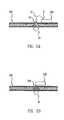
- FIG. 2Aa semiconductor package formed using substrate 10 K is shown.
- a die 30 Ais mounted to substrate 10 K, generally with an adhesive film or epoxy and wires 32 are bonded between electrical terminals 31 of the die 30 A and bond pads 33 on substrate 10 K.
- Solder balls 34are attached to lands on the bottom side of substrate 10 K to form a ball grid array package, which can then be encapsulated on the top side.
- FIG. 2BAn alternative semiconductor package is shown in FIG. 2B , where a die 30 B is mounted in a flip-chip configuration using solder balls 34 A or alternatively solder posts.
- FIGS. 2A and 2Bare intended to be illustrative of semiconductor packages (packaged integrated circuits) that may be manufactured in accordance with embodiments of the present invention and are thus not intended to be limiting.
- the techniques of the present inventionhave applications to other semiconductor package types and die types, as the two-level homogeneous metal circuit produced by the techniques of the present invention provides higher interconnect density in a low-cost manufacturing process.
- a dielectric layer 42includes metal circuit channel areas 44 formed within dielectric layer 42 (via laser-ablation, plating and etching) and metal circuit surface areas 46 formed atop dielectric layer 42 (via plating and etching).
- Area A 1illustrates an area where the metal circuit is channel level only
- area A 2illustrates an area where the metal circuit is above-surface level only (in the illustration, actually below the opposite surface)
- area A 3illustrates an area where the metal circuit bridges the two levels to provide a conductive path from a channel to a surface feature. All of the illustrations described above are for a double-sided substrate, but a single sided substrate may also be produced by selectively plating a dielectric layer that has been laser ablated on one side.
- FIG. 3Bdepicts an extension of the present invention to a multi-layer multi-level structure. Additional dielectric layers 52 A and 52 B may be laminated on a dielectric layer 52 prepared with two-level circuits in accordance with an embodiment of the present invention. Then, additional dielectric layers 52 A and 52 B may be subjected to the above-described process to generate two more outer two-level layers 56 A and 56 B having channels and surface-located features. Connections between circuit layers are provide by vias 54 A such as those vias 54 B used to connect the two-level structures on opposite sides of original dielectric layer 52 .
- circuit channels and terminalsWhile the figures illustrate conductive circuit channels and above surface features, the figures are depicting only a portion of the total substrate. Hundreds of circuit channels and terminals will generally be used in an integrated circuit design and may be oriented in any direction within the surface of the substrate. Similarly, the pattern above the substrate surface may include terminal lands only, or may include circuit patterns as well.
- the pattern atop the substrateshould be designed so that channel conductors are appropriately isolated when the metal is removed, and so unless two channels are to be electrically bridged, the pattern level above the substrate does not cross both of those channels, as electrical contact is made between a channel and the level above the substrate when any metal is present at both levels (i.e., when the circuit-positive photomask for the top layer intersects the channel ablating pattern at any point in the two-dimensional plane of the substrate surface).
Landscapes
- Engineering & Computer Science (AREA)
- Microelectronics & Electronic Packaging (AREA)
- Manufacturing & Machinery (AREA)
- Power Engineering (AREA)
- Computer Hardware Design (AREA)
- Condensed Matter Physics & Semiconductors (AREA)
- General Physics & Mathematics (AREA)
- Physics & Mathematics (AREA)
- Ceramic Engineering (AREA)
- Structures For Mounting Electric Components On Printed Circuit Boards (AREA)
- Manufacturing Of Printed Wiring (AREA)
- Manufacturing Of Printed Circuit Boards (AREA)
- Production Of Multi-Layered Print Wiring Board (AREA)
Abstract
Description
Claims (20)
Priority Applications (1)
| Application Number | Priority Date | Filing Date | Title |
|---|---|---|---|
| US12/151,857US8316536B1 (en) | 2002-05-01 | 2008-05-09 | Multi-level circuit substrate fabrication method |
Applications Claiming Priority (3)
| Application Number | Priority Date | Filing Date | Title |
|---|---|---|---|
| US10/138,225US6930256B1 (en) | 2002-05-01 | 2002-05-01 | Integrated circuit substrate having laser-embedded conductive patterns and method therefor |
| US4540205A | 2005-01-28 | 2005-01-28 | |
| US12/151,857US8316536B1 (en) | 2002-05-01 | 2008-05-09 | Multi-level circuit substrate fabrication method |
Related Parent Applications (1)
| Application Number | Title | Priority Date | Filing Date |
|---|---|---|---|
| US4540205AContinuation | 2002-05-01 | 2005-01-28 |
Publications (1)
| Publication Number | Publication Date |
|---|---|
| US8316536B1true US8316536B1 (en) | 2012-11-27 |
Family
ID=34825506
Family Applications (9)
| Application Number | Title | Priority Date | Filing Date |
|---|---|---|---|
| US10/138,225Expired - LifetimeUS6930256B1 (en) | 2001-06-19 | 2002-05-01 | Integrated circuit substrate having laser-embedded conductive patterns and method therefor |
| US10/806,640Expired - LifetimeUS7185426B1 (en) | 2002-05-01 | 2004-03-23 | Method of manufacturing a semiconductor package |
| US11/021,977Expired - LifetimeUS7312103B1 (en) | 2002-05-01 | 2004-12-22 | Method for making an integrated circuit substrate having laser-embedded conductive patterns |
| US11/166,005Expired - LifetimeUS7297562B1 (en) | 2002-05-01 | 2005-06-24 | Circuit-on-foil process for manufacturing a laminated semiconductor package substrate having embedded conductive patterns |
| US11/595,411Expired - LifetimeUS7671457B1 (en) | 2002-05-01 | 2006-11-09 | Semiconductor package including top-surface terminals for mounting another semiconductor package |
| US11/982,637Expired - LifetimeUS8322030B1 (en) | 2002-05-01 | 2007-11-01 | Circuit-on-foil process for manufacturing a laminated semiconductor package substrate having embedded conductive patterns |
| US12/151,857Expired - Fee RelatedUS8316536B1 (en) | 2002-05-01 | 2008-05-09 | Multi-level circuit substrate fabrication method |
| US12/655,724Expired - LifetimeUS8110909B1 (en) | 2002-05-01 | 2010-01-05 | Semiconductor package including top-surface terminals for mounting another semiconductor package |
| US12/802,661Expired - LifetimeUS8026587B1 (en) | 2002-05-01 | 2010-06-10 | Semiconductor package including top-surface terminals for mounting another semiconductor package |
Family Applications Before (6)
| Application Number | Title | Priority Date | Filing Date |
|---|---|---|---|
| US10/138,225Expired - LifetimeUS6930256B1 (en) | 2001-06-19 | 2002-05-01 | Integrated circuit substrate having laser-embedded conductive patterns and method therefor |
| US10/806,640Expired - LifetimeUS7185426B1 (en) | 2002-05-01 | 2004-03-23 | Method of manufacturing a semiconductor package |
| US11/021,977Expired - LifetimeUS7312103B1 (en) | 2002-05-01 | 2004-12-22 | Method for making an integrated circuit substrate having laser-embedded conductive patterns |
| US11/166,005Expired - LifetimeUS7297562B1 (en) | 2002-05-01 | 2005-06-24 | Circuit-on-foil process for manufacturing a laminated semiconductor package substrate having embedded conductive patterns |
| US11/595,411Expired - LifetimeUS7671457B1 (en) | 2002-05-01 | 2006-11-09 | Semiconductor package including top-surface terminals for mounting another semiconductor package |
| US11/982,637Expired - LifetimeUS8322030B1 (en) | 2002-05-01 | 2007-11-01 | Circuit-on-foil process for manufacturing a laminated semiconductor package substrate having embedded conductive patterns |
Family Applications After (2)
| Application Number | Title | Priority Date | Filing Date |
|---|---|---|---|
| US12/655,724Expired - LifetimeUS8110909B1 (en) | 2002-05-01 | 2010-01-05 | Semiconductor package including top-surface terminals for mounting another semiconductor package |
| US12/802,661Expired - LifetimeUS8026587B1 (en) | 2002-05-01 | 2010-06-10 | Semiconductor package including top-surface terminals for mounting another semiconductor package |
Country Status (1)
| Country | Link |
|---|---|
| US (9) | US6930256B1 (en) |
Cited By (6)
| Publication number | Priority date | Publication date | Assignee | Title |
|---|---|---|---|---|
| US9462704B1 (en) | 2009-01-09 | 2016-10-04 | Amkor Technology, Inc. | Extended landing pad substrate package structure and method |
| US9812386B1 (en) | 2002-05-01 | 2017-11-07 | Amkor Technology, Inc. | Encapsulated semiconductor package |
| CN110798987A (en)* | 2018-08-01 | 2020-02-14 | 宏启胜精密电子(秦皇岛)有限公司 | Circuit board and method for manufacturing the same |
| US10811277B2 (en) | 2004-03-23 | 2020-10-20 | Amkor Technology, Inc. | Encapsulated semiconductor package |
| US11081370B2 (en) | 2004-03-23 | 2021-08-03 | Amkor Technology Singapore Holding Pte. Ltd. | Methods of manufacturing an encapsulated semiconductor device |
| US11094560B1 (en) | 2004-03-23 | 2021-08-17 | Amkor Technology Singapore Holding Pte. Ltd. | Encapsulated semiconductor package |
Families Citing this family (290)
| Publication number | Priority date | Publication date | Assignee | Title |
|---|---|---|---|---|
| US6143981A (en) | 1998-06-24 | 2000-11-07 | Amkor Technology, Inc. | Plastic integrated circuit package and method and leadframe for making the package |
| US7332375B1 (en) | 1998-06-24 | 2008-02-19 | Amkor Technology, Inc. | Method of making an integrated circuit package |
| TW512467B (en)* | 1999-10-12 | 2002-12-01 | North Kk | Wiring circuit substrate and manufacturing method therefor |
| KR100369393B1 (en)* | 2001-03-27 | 2003-02-05 | 앰코 테크놀로지 코리아 주식회사 | Lead frame and semiconductor package using it and its manufacturing method |
| US6930256B1 (en) | 2002-05-01 | 2005-08-16 | Amkor Technology, Inc. | Integrated circuit substrate having laser-embedded conductive patterns and method therefor |
| US7670962B2 (en) | 2002-05-01 | 2010-03-02 | Amkor Technology, Inc. | Substrate having stiffener fabrication method |
| US7399661B2 (en)* | 2002-05-01 | 2008-07-15 | Amkor Technology, Inc. | Method for making an integrated circuit substrate having embedded back-side access conductors and vias |
| US20080043447A1 (en)* | 2002-05-01 | 2008-02-21 | Amkor Technology, Inc. | Semiconductor package having laser-embedded terminals |
| US7633765B1 (en) | 2004-03-23 | 2009-12-15 | Amkor Technology, Inc. | Semiconductor package including a top-surface metal layer for implementing circuit features |
| US20040011555A1 (en)* | 2002-07-22 | 2004-01-22 | Chiu Tsung Chin | Method for manufacturing printed circuit board with stacked wires and printed circuit board manufacturing according to the mehtod |
| US7361533B1 (en) | 2002-11-08 | 2008-04-22 | Amkor Technology, Inc. | Stacked embedded leadframe |
| US7723210B2 (en) | 2002-11-08 | 2010-05-25 | Amkor Technology, Inc. | Direct-write wafer level chip scale package |
| US6905914B1 (en) | 2002-11-08 | 2005-06-14 | Amkor Technology, Inc. | Wafer level package and fabrication method |
| US7371975B2 (en)* | 2002-12-18 | 2008-05-13 | Intel Corporation | Electronic packages and components thereof formed by substrate-imprinting |
| US7637008B2 (en)* | 2002-12-18 | 2009-12-29 | Intel Corporation | Methods for manufacturing imprinted substrates |
| US20040126547A1 (en)* | 2002-12-31 | 2004-07-01 | Coomer Boyd L. | Methods for performing substrate imprinting using thermoset resin varnishes and products formed therefrom |
| DE102004005300A1 (en)* | 2004-01-29 | 2005-09-08 | Atotech Deutschland Gmbh | Process for treating carrier material for the production of powder carriers and application of the process |
| JP2005317861A (en)* | 2004-04-30 | 2005-11-10 | Toshiba Corp | Semiconductor device and manufacturing method thereof |
| US7145238B1 (en) | 2004-05-05 | 2006-12-05 | Amkor Technology, Inc. | Semiconductor package and substrate having multi-level vias |
| US7553680B2 (en)* | 2004-08-09 | 2009-06-30 | Delphi Technologies, Inc. | Methods to provide and expose a diagnostic connector on overmolded electronic packages |
| DE102004049654B3 (en)* | 2004-10-11 | 2006-04-13 | Infineon Technologies Ag | Semiconductor device with plastic housing and method for producing the same |
| KR101313391B1 (en) | 2004-11-03 | 2013-10-01 | 테세라, 인코포레이티드 | Stacked packaging improvements |
| JP4649198B2 (en)* | 2004-12-20 | 2011-03-09 | 新光電気工業株式会社 | Wiring board manufacturing method |
| US8826531B1 (en) | 2005-04-05 | 2014-09-09 | Amkor Technology, Inc. | Method for making an integrated circuit substrate having laminated laser-embedded circuit layers |
| US7507603B1 (en) | 2005-12-02 | 2009-03-24 | Amkor Technology, Inc. | Etch singulated semiconductor package |
| US7572681B1 (en) | 2005-12-08 | 2009-08-11 | Amkor Technology, Inc. | Embedded electronic component package |
| US8058101B2 (en) | 2005-12-23 | 2011-11-15 | Tessera, Inc. | Microelectronic packages and methods therefor |
| SG135074A1 (en) | 2006-02-28 | 2007-09-28 | Micron Technology Inc | Microelectronic devices, stacked microelectronic devices, and methods for manufacturing such devices |
| US8072059B2 (en)* | 2006-04-19 | 2011-12-06 | Stats Chippac, Ltd. | Semiconductor device and method of forming UBM fixed relative to interconnect structure for alignment of semiconductor die |
| US7859098B2 (en)* | 2006-04-19 | 2010-12-28 | Stats Chippac Ltd. | Embedded integrated circuit package system |
| US8546929B2 (en)* | 2006-04-19 | 2013-10-01 | Stats Chippac Ltd. | Embedded integrated circuit package-on-package system |
| US7902660B1 (en) | 2006-05-24 | 2011-03-08 | Amkor Technology, Inc. | Substrate for semiconductor device and manufacturing method thereof |
| US7968998B1 (en) | 2006-06-21 | 2011-06-28 | Amkor Technology, Inc. | Side leaded, bottom exposed pad and bottom exposed lead fusion quad flat semiconductor package |
| US7459202B2 (en)* | 2006-07-03 | 2008-12-02 | Motorola, Inc. | Printed circuit board |
| TWI336502B (en)* | 2006-09-27 | 2011-01-21 | Advanced Semiconductor Eng | Semiconductor package and semiconductor device and the method of making the same |
| US7589398B1 (en) | 2006-10-04 | 2009-09-15 | Amkor Technology, Inc. | Embedded metal features structure |
| US7550857B1 (en) | 2006-11-16 | 2009-06-23 | Amkor Technology, Inc. | Stacked redistribution layer (RDL) die assembly package |
| US7608538B2 (en) | 2007-01-05 | 2009-10-27 | International Business Machines Corporation | Formation of vertical devices by electroplating |
| US7752752B1 (en) | 2007-01-09 | 2010-07-13 | Amkor Technology, Inc. | Method of fabricating an embedded circuit pattern |
| TWI335070B (en) | 2007-03-23 | 2010-12-21 | Advanced Semiconductor Eng | Semiconductor package and the method of making the same |
| US20080284045A1 (en)* | 2007-05-18 | 2008-11-20 | Texas Instruments Incorporated | Method for Fabricating Array-Molded Package-On-Package |
| JP4588046B2 (en)* | 2007-05-31 | 2010-11-24 | 三洋電機株式会社 | Circuit device and manufacturing method thereof |
| US7944034B2 (en)* | 2007-06-22 | 2011-05-17 | Texas Instruments Incorporated | Array molded package-on-package having redistribution lines |
| US7977774B2 (en) | 2007-07-10 | 2011-07-12 | Amkor Technology, Inc. | Fusion quad flat semiconductor package |
| US7687899B1 (en) | 2007-08-07 | 2010-03-30 | Amkor Technology, Inc. | Dual laminate package structure with embedded elements |
| JP5358077B2 (en)* | 2007-09-28 | 2013-12-04 | スパンション エルエルシー | Semiconductor device and manufacturing method thereof |
| US8481366B2 (en)* | 2007-09-28 | 2013-07-09 | Spansion Llc | Semiconductor device and manufacturing method therefor |
| US7777351B1 (en) | 2007-10-01 | 2010-08-17 | Amkor Technology, Inc. | Thin stacked interposer package |
| US8089159B1 (en) | 2007-10-03 | 2012-01-03 | Amkor Technology, Inc. | Semiconductor package with increased I/O density and method of making the same |
| KR101572600B1 (en) | 2007-10-10 | 2015-11-27 | 테세라, 인코포레이티드 | Robust multi-layer wiring elements and assemblies with embedded microelectronic elements |
| TWI360207B (en)* | 2007-10-22 | 2012-03-11 | Advanced Semiconductor Eng | Chip package structure and method of manufacturing |
| JP5081578B2 (en)* | 2007-10-25 | 2012-11-28 | ローム株式会社 | Resin-sealed semiconductor device |
| US7847386B1 (en) | 2007-11-05 | 2010-12-07 | Amkor Technology, Inc. | Reduced size stacked semiconductor package and method of making the same |
| US20090140408A1 (en)* | 2007-11-30 | 2009-06-04 | Taewoo Lee | Integrated circuit package-on-package system with stacking via interconnect |
| US8017436B1 (en)* | 2007-12-10 | 2011-09-13 | Amkor Technology, Inc. | Thin substrate fabrication method and structure |
| SG153762A1 (en)* | 2007-12-12 | 2009-07-29 | United Test & Assembly Ct Ltd | Package-on-package semiconductor structure |
| US7956453B1 (en) | 2008-01-16 | 2011-06-07 | Amkor Technology, Inc. | Semiconductor package with patterning layer and method of making same |
| US7723852B1 (en) | 2008-01-21 | 2010-05-25 | Amkor Technology, Inc. | Stacked semiconductor package and method of making same |
| US8120186B2 (en)* | 2008-02-15 | 2012-02-21 | Qimonda Ag | Integrated circuit and method |
| US7863755B2 (en)* | 2008-03-19 | 2011-01-04 | Stats Chippac Ltd. | Package-on-package system with via Z-interconnections |
| US8067821B1 (en) | 2008-04-10 | 2011-11-29 | Amkor Technology, Inc. | Flat semiconductor package with half package molding |
| US7768135B1 (en) | 2008-04-17 | 2010-08-03 | Amkor Technology, Inc. | Semiconductor package with fast power-up cycle and method of making same |
| US7808084B1 (en) | 2008-05-06 | 2010-10-05 | Amkor Technology, Inc. | Semiconductor package with half-etched locking features |
| US7888184B2 (en)* | 2008-06-20 | 2011-02-15 | Stats Chippac Ltd. | Integrated circuit packaging system with embedded circuitry and post, and method of manufacture thereof |
| TWI473553B (en)* | 2008-07-03 | 2015-02-11 | Advanced Semiconductor Eng | Chip package structure |
| TWI453877B (en)* | 2008-11-07 | 2014-09-21 | Advanced Semiconductor Eng | Structure and process of embedded chip package |
| US8441804B2 (en)* | 2008-07-25 | 2013-05-14 | Infineon Technologies Ag | Semiconductor device and method of manufacturing a semiconductor device |
| US8125064B1 (en) | 2008-07-28 | 2012-02-28 | Amkor Technology, Inc. | Increased I/O semiconductor package and method of making same |
| US8184453B1 (en) | 2008-07-31 | 2012-05-22 | Amkor Technology, Inc. | Increased capacity semiconductor package |
| US8132321B2 (en) | 2008-08-13 | 2012-03-13 | Unimicron Technology Corp. | Method for making embedded circuit structure |
| US8191248B2 (en)* | 2008-09-17 | 2012-06-05 | Unimicron Technology Corp. | Method for making an embedded structure |
| TWI430722B (en)* | 2008-09-05 | 2014-03-11 | Unimicron Technology Corp | Circuit structure of circuit board and process thereof |
| US9164404B2 (en) | 2008-09-19 | 2015-10-20 | Intel Corporation | System and process for fabricating semiconductor packages |
| US9165841B2 (en)* | 2008-09-19 | 2015-10-20 | Intel Corporation | System and process for fabricating semiconductor packages |
| US7842541B1 (en) | 2008-09-24 | 2010-11-30 | Amkor Technology, Inc. | Ultra thin package and fabrication method |
| US8076587B2 (en)* | 2008-09-26 | 2011-12-13 | Siemens Energy, Inc. | Printed circuit board for harsh environments |
| US7847392B1 (en) | 2008-09-30 | 2010-12-07 | Amkor Technology, Inc. | Semiconductor device including leadframe with increased I/O |
| US8365402B2 (en)* | 2008-09-30 | 2013-02-05 | Ibiden Co., Ltd. | Method for manufacturing printed wiring board |
| US7989933B1 (en) | 2008-10-06 | 2011-08-02 | Amkor Technology, Inc. | Increased I/O leadframe and semiconductor device including same |
| US8008758B1 (en) | 2008-10-27 | 2011-08-30 | Amkor Technology, Inc. | Semiconductor device with increased I/O leadframe |
| US8089145B1 (en) | 2008-11-17 | 2012-01-03 | Amkor Technology, Inc. | Semiconductor device including increased capacity leadframe |
| US8072050B1 (en) | 2008-11-18 | 2011-12-06 | Amkor Technology, Inc. | Semiconductor device with increased I/O leadframe including passive device |
| US7875963B1 (en) | 2008-11-21 | 2011-01-25 | Amkor Technology, Inc. | Semiconductor device including leadframe having power bars and increased I/O |
| US7982298B1 (en) | 2008-12-03 | 2011-07-19 | Amkor Technology, Inc. | Package in package semiconductor device |
| US8354304B2 (en)* | 2008-12-05 | 2013-01-15 | Stats Chippac, Ltd. | Semiconductor device and method of forming conductive posts embedded in photosensitive encapsulant |
| US8487420B1 (en) | 2008-12-08 | 2013-07-16 | Amkor Technology, Inc. | Package in package semiconductor device with film over wire |
| US20170117214A1 (en)* | 2009-01-05 | 2017-04-27 | Amkor Technology, Inc. | Semiconductor device with through-mold via |
| US8680656B1 (en) | 2009-01-05 | 2014-03-25 | Amkor Technology, Inc. | Leadframe structure for concentrated photovoltaic receiver package |
| TWI499024B (en)* | 2009-01-07 | 2015-09-01 | Advanced Semiconductor Eng | Package-on-package device, semiconductor package and method for manufacturing the same |
| US20100171206A1 (en)* | 2009-01-07 | 2010-07-08 | Chi-Chih Chu | Package-on-Package Device, Semiconductor Package, and Method for Manufacturing The Same |
| US8012797B2 (en)* | 2009-01-07 | 2011-09-06 | Advanced Semiconductor Engineering, Inc. | Method for forming stackable semiconductor device packages including openings with conductive bumps of specified geometries |
| KR101006603B1 (en)* | 2009-01-09 | 2011-01-07 | 삼성전기주식회사 | Printed circuit board and manufacturing method thereof |
| US8058715B1 (en) | 2009-01-09 | 2011-11-15 | Amkor Technology, Inc. | Package in package device for RF transceiver module |
| US20100193930A1 (en)* | 2009-02-02 | 2010-08-05 | Samsung Electronics Co., Ltd. | Multi-chip semiconductor devices having conductive vias and methods of forming the same |
| US8026589B1 (en) | 2009-02-23 | 2011-09-27 | Amkor Technology, Inc. | Reduced profile stackable semiconductor package |
| US7960818B1 (en) | 2009-03-04 | 2011-06-14 | Amkor Technology, Inc. | Conformal shield on punch QFN semiconductor package |
| TWI384925B (en)* | 2009-03-17 | 2013-02-01 | Advanced Semiconductor Eng | Structure of embedded-trace substrate and method of manufacturing the same |
| US8575742B1 (en) | 2009-04-06 | 2013-11-05 | Amkor Technology, Inc. | Semiconductor device with increased I/O leadframe including power bars |
| KR20100112446A (en)* | 2009-04-09 | 2010-10-19 | 삼성전자주식회사 | Stacked semiconductor package and manufacturing method thereof |
| US7960827B1 (en) | 2009-04-09 | 2011-06-14 | Amkor Technology, Inc. | Thermal via heat spreader package and method |
| US8623753B1 (en)* | 2009-05-28 | 2014-01-07 | Amkor Technology, Inc. | Stackable protruding via package and method |
| US9355962B2 (en)* | 2009-06-12 | 2016-05-31 | Stats Chippac Ltd. | Integrated circuit package stacking system with redistribution and method of manufacture thereof |
| US8222538B1 (en) | 2009-06-12 | 2012-07-17 | Amkor Technology, Inc. | Stackable via package and method |
| US8241955B2 (en) | 2009-06-19 | 2012-08-14 | Stats Chippac Ltd. | Integrated circuit packaging system with mountable inward and outward interconnects and method of manufacture thereof |
| US7927917B2 (en)* | 2009-06-19 | 2011-04-19 | Stats Chippac Ltd. | Integrated circuit packaging system with inward and outward interconnects and method of manufacture thereof |
| US8471154B1 (en) | 2009-08-06 | 2013-06-25 | Amkor Technology, Inc. | Stackable variable height via package and method |
| TWI469283B (en)* | 2009-08-31 | 2015-01-11 | Advanced Semiconductor Eng | Package structure and package process |
| US7923304B2 (en)* | 2009-09-10 | 2011-04-12 | Stats Chippac Ltd. | Integrated circuit packaging system with conductive pillars and method of manufacture thereof |
| US8264091B2 (en)* | 2009-09-21 | 2012-09-11 | Stats Chippac Ltd. | Integrated circuit packaging system with encapsulated via and method of manufacture thereof |
| US8796561B1 (en) | 2009-10-05 | 2014-08-05 | Amkor Technology, Inc. | Fan out build up substrate stackable package and method |
| KR20110044077A (en)* | 2009-10-22 | 2011-04-28 | 삼성전자주식회사 | Semiconductor package structure |
| US20110094778A1 (en)* | 2009-10-27 | 2011-04-28 | Cheng-Po Yu | Circuit board and fabrication method thereof |
| US9941195B2 (en)* | 2009-11-10 | 2018-04-10 | Taiwan Semiconductor Manufacturing Co., Ltd. | Vertical metal insulator metal capacitor |
| KR101047139B1 (en)* | 2009-11-11 | 2011-07-07 | 삼성전기주식회사 | Single Layer Board-on-Chip Package Substrate and Manufacturing Method Thereof |
| US8198131B2 (en)* | 2009-11-18 | 2012-06-12 | Advanced Semiconductor Engineering, Inc. | Stackable semiconductor device packages |
| US8327532B2 (en)* | 2009-11-23 | 2012-12-11 | Freescale Semiconductor, Inc. | Method for releasing a microelectronic assembly from a carrier substrate |
| US8937381B1 (en) | 2009-12-03 | 2015-01-20 | Amkor Technology, Inc. | Thin stackable package and method |
| US9691734B1 (en) | 2009-12-07 | 2017-06-27 | Amkor Technology, Inc. | Method of forming a plurality of electronic component packages |
| US8390108B2 (en)* | 2009-12-16 | 2013-03-05 | Stats Chippac Ltd. | Integrated circuit packaging system with stacking interconnect and method of manufacture thereof |
| US8987896B2 (en)* | 2009-12-16 | 2015-03-24 | Intel Corporation | High-density inter-package connections for ultra-thin package-on-package structures, and processes of forming same |
| US8508954B2 (en) | 2009-12-17 | 2013-08-13 | Samsung Electronics Co., Ltd. | Systems employing a stacked semiconductor package |
| TWI405515B (en)* | 2009-12-30 | 2013-08-11 | Unimicron Technology Corp | Circuit board and manufacturing method thereof |
| TWI408785B (en)* | 2009-12-31 | 2013-09-11 | Advanced Semiconductor Eng | Semiconductor package |
| US8569894B2 (en) | 2010-01-13 | 2013-10-29 | Advanced Semiconductor Engineering, Inc. | Semiconductor package with single sided substrate design and manufacturing methods thereof |
| US8536462B1 (en) | 2010-01-22 | 2013-09-17 | Amkor Technology, Inc. | Flex circuit package and method |
| US8320134B2 (en) | 2010-02-05 | 2012-11-27 | Advanced Semiconductor Engineering, Inc. | Embedded component substrate and manufacturing methods thereof |
| TWI419283B (en)* | 2010-02-10 | 2013-12-11 | Advanced Semiconductor Eng | Package structure |
| US8497575B2 (en)* | 2010-02-22 | 2013-07-30 | Stats Chippac Ltd. | Semiconductor packaging system with an aligned interconnect and method of manufacture thereof |
| TWI411075B (en) | 2010-03-22 | 2013-10-01 | Advanced Semiconductor Eng | Semiconductor package and manufacturing method thereof |
| US8643181B2 (en)* | 2010-03-24 | 2014-02-04 | Stats Chippac Ltd. | Integrated circuit packaging system with encapsulation and method of manufacture thereof |
| US8378476B2 (en)* | 2010-03-25 | 2013-02-19 | Stats Chippac Ltd. | Integrated circuit packaging system with stacking option and method of manufacture thereof |
| US8624374B2 (en) | 2010-04-02 | 2014-01-07 | Advanced Semiconductor Engineering, Inc. | Semiconductor device packages with fan-out and with connecting elements for stacking and manufacturing methods thereof |
| US8278746B2 (en) | 2010-04-02 | 2012-10-02 | Advanced Semiconductor Engineering, Inc. | Semiconductor device packages including connecting elements |
| US8324511B1 (en) | 2010-04-06 | 2012-12-04 | Amkor Technology, Inc. | Through via nub reveal method and structure |
| KR101078743B1 (en)* | 2010-04-14 | 2011-11-02 | 주식회사 하이닉스반도체 | stack package |
| KR101096271B1 (en) | 2010-04-21 | 2011-12-22 | 주식회사 하이닉스반도체 | Semiconductor package having a structure of package on package and method of fabricating the same |
| US8618731B2 (en)* | 2010-05-18 | 2013-12-31 | General Electric Company | Large-area flexible OLED light source |
| US8300423B1 (en) | 2010-05-25 | 2012-10-30 | Amkor Technology, Inc. | Stackable treated via package and method |
| US8294276B1 (en) | 2010-05-27 | 2012-10-23 | Amkor Technology, Inc. | Semiconductor device and fabricating method thereof |
| CN102310602B (en)* | 2010-06-30 | 2014-03-26 | 鸿富锦精密工业(深圳)有限公司 | Aluminium-plastic composite structure and manufacture method thereof |
| US8482111B2 (en) | 2010-07-19 | 2013-07-09 | Tessera, Inc. | Stackable molded microelectronic packages |
| US9159708B2 (en) | 2010-07-19 | 2015-10-13 | Tessera, Inc. | Stackable molded microelectronic packages with area array unit connectors |
| KR101119348B1 (en)* | 2010-07-23 | 2012-03-07 | 삼성전기주식회사 | Semiconductor module and manufactureing method thereof |
| TWI436713B (en)* | 2010-07-26 | 2014-05-01 | Via Tech Inc | Circuit substrate, fabricating process of circuit substrate |
| US8338229B1 (en) | 2010-07-30 | 2012-12-25 | Amkor Technology, Inc. | Stackable plasma cleaned via package and method |
| US8440554B1 (en) | 2010-08-02 | 2013-05-14 | Amkor Technology, Inc. | Through via connected backside embedded circuit features structure and method |
| US8717775B1 (en) | 2010-08-02 | 2014-05-06 | Amkor Technology, Inc. | Fingerprint sensor package and method |
| US8895440B2 (en)* | 2010-08-06 | 2014-11-25 | Stats Chippac, Ltd. | Semiconductor die and method of forming Fo-WLCSP vertical interconnect using TSV and TMV |
| KR20120031697A (en)* | 2010-09-27 | 2012-04-04 | 삼성전자주식회사 | Package stack structures and methods of fabricating the same |
| US8487445B1 (en) | 2010-10-05 | 2013-07-16 | Amkor Technology, Inc. | Semiconductor device having through electrodes protruding from dielectric layer |
| TWI501365B (en)* | 2010-10-13 | 2015-09-21 | Ind Tech Res Inst | Package unit, stacking structure thereof and manufacturing method thereof |
| KR101796116B1 (en) | 2010-10-20 | 2017-11-10 | 삼성전자 주식회사 | Semiconductor device, memory module and memory system having the same and operating method thereof |
| US8337657B1 (en) | 2010-10-27 | 2012-12-25 | Amkor Technology, Inc. | Mechanical tape separation package and method |
| US8263435B2 (en)* | 2010-10-28 | 2012-09-11 | Stats Chippac, Ltd. | Semiconductor device and method of stacking semiconductor die in mold laser package interconnected by bumps and conductive vias |
| TWI451546B (en) | 2010-10-29 | 2014-09-01 | Advanced Semiconductor Eng | Stacked semiconductor package, semiconductor package thereof and method for making a semiconductor package |
| US8482134B1 (en) | 2010-11-01 | 2013-07-09 | Amkor Technology, Inc. | Stackable package and method |
| US9748154B1 (en) | 2010-11-04 | 2017-08-29 | Amkor Technology, Inc. | Wafer level fan out semiconductor device and manufacturing method thereof |
| US8525318B1 (en) | 2010-11-10 | 2013-09-03 | Amkor Technology, Inc. | Semiconductor device and fabricating method thereof |
| KR101075241B1 (en) | 2010-11-15 | 2011-11-01 | 테세라, 인코포레이티드 | Microelectronic package with terminals in dielectric member |
| US8288202B2 (en) | 2010-11-22 | 2012-10-16 | STATS ChiPAC, Ltd. | Method of forming partially-etched conductive layer recessed within substrate for bonding to semiconductor die |
| US8791501B1 (en) | 2010-12-03 | 2014-07-29 | Amkor Technology, Inc. | Integrated passive device structure and method |
| US8557629B1 (en) | 2010-12-03 | 2013-10-15 | Amkor Technology, Inc. | Semiconductor device having overlapped via apertures |
| US8674485B1 (en) | 2010-12-08 | 2014-03-18 | Amkor Technology, Inc. | Semiconductor device including leadframe with downsets |
| US8502387B2 (en) | 2010-12-09 | 2013-08-06 | Stats Chippac Ltd. | Integrated circuit packaging system with vertical interconnection and method of manufacture thereof |
| US8535961B1 (en) | 2010-12-09 | 2013-09-17 | Amkor Technology, Inc. | Light emitting diode (LED) package and method |
| US20120146206A1 (en) | 2010-12-13 | 2012-06-14 | Tessera Research Llc | Pin attachment |
| US9406658B2 (en) | 2010-12-17 | 2016-08-02 | Advanced Semiconductor Engineering, Inc. | Embedded component device and manufacturing methods thereof |
| KR101719630B1 (en) | 2010-12-21 | 2017-04-04 | 삼성전자 주식회사 | Semiconductor package and package on package comprising them |
| KR101181048B1 (en)* | 2010-12-27 | 2012-09-07 | 엘지이노텍 주식회사 | The method for manufacturing the printed circuit board |
| US8390130B1 (en) | 2011-01-06 | 2013-03-05 | Amkor Technology, Inc. | Through via recessed reveal structure and method |
| TWI445155B (en) | 2011-01-06 | 2014-07-11 | Advanced Semiconductor Eng | Stacked semiconductor package and method for making the same |
| US8648450B1 (en) | 2011-01-27 | 2014-02-11 | Amkor Technology, Inc. | Semiconductor device including leadframe with a combination of leads and lands |
| TWI557183B (en) | 2015-12-16 | 2016-11-11 | 財團法人工業技術研究院 | Oxane composition, and photovoltaic device comprising the same |
| US9721872B1 (en) | 2011-02-18 | 2017-08-01 | Amkor Technology, Inc. | Methods and structures for increasing the allowable die size in TMV packages |
| US9171792B2 (en) | 2011-02-28 | 2015-10-27 | Advanced Semiconductor Engineering, Inc. | Semiconductor device packages having a side-by-side device arrangement and stacking functionality |
| US9013011B1 (en) | 2011-03-11 | 2015-04-21 | Amkor Technology, Inc. | Stacked and staggered die MEMS package and method |
| US8487426B2 (en) | 2011-03-15 | 2013-07-16 | Advanced Semiconductor Engineering, Inc. | Semiconductor package with embedded die and manufacturing methods thereof |
| TWI503060B (en)* | 2011-03-30 | 2015-10-01 | Mitsui Mining & Smelting Co | Method of manufacturing multi-layer printed wiring board and multi-layer printed wiring board obtained by the manufacturing method |
| KR101140113B1 (en) | 2011-04-26 | 2012-04-30 | 앰코 테크놀로지 코리아 주식회사 | Semiconductor device |
| KR101128063B1 (en) | 2011-05-03 | 2012-04-23 | 테세라, 인코포레이티드 | Package-on-package assembly with wire bonds to encapsulation surface |
| US8618659B2 (en) | 2011-05-03 | 2013-12-31 | Tessera, Inc. | Package-on-package assembly with wire bonds to encapsulation surface |
| US8476135B2 (en) | 2011-05-27 | 2013-07-02 | Stats Chippac Ltd. | Integrated circuit packaging system with vertical interconnects and method of manufacture thereof |
| US8765525B2 (en) | 2011-06-16 | 2014-07-01 | Stats Chippac Ltd. | Method of manufacturing an integrated circuit packaging system including lasering through encapsulant over interposer |
| US8633100B2 (en) | 2011-06-17 | 2014-01-21 | Stats Chippac Ltd. | Method of manufacturing integrated circuit packaging system with support structure |
| US8754514B2 (en) | 2011-08-10 | 2014-06-17 | Taiwan Semiconductor Manufacturing Company, Ltd. | Multi-chip wafer level package |
| US20130040423A1 (en)* | 2011-08-10 | 2013-02-14 | Taiwan Semiconductor Manufacturing Company, Ltd. | Method of Multi-Chip Wafer Level Packaging |
| US8872318B2 (en) | 2011-08-24 | 2014-10-28 | Tessera, Inc. | Through interposer wire bond using low CTE interposer with coarse slot apertures |
| US8916421B2 (en) | 2011-08-31 | 2014-12-23 | Freescale Semiconductor, Inc. | Semiconductor device packaging having pre-encapsulation through via formation using lead frames with attached signal conduits |
| US9142502B2 (en) | 2011-08-31 | 2015-09-22 | Zhiwei Gong | Semiconductor device packaging having pre-encapsulation through via formation using drop-in signal conduits |
| US8653674B1 (en) | 2011-09-15 | 2014-02-18 | Amkor Technology, Inc. | Electronic component package fabrication method and structure |
| US8513057B2 (en) | 2011-09-16 | 2013-08-20 | Stats Chippac Ltd. | Integrated circuit packaging system with routable underlayer and method of manufacture thereof |
| US8603859B2 (en) | 2011-09-16 | 2013-12-10 | Stats Chippac Ltd. | Integrated circuit packaging system with dual side mold and method of manufacture thereof |
| US8633598B1 (en) | 2011-09-20 | 2014-01-21 | Amkor Technology, Inc. | Underfill contacting stacking balls package fabrication method and structure |
| US8716065B2 (en) | 2011-09-23 | 2014-05-06 | Stats Chippac Ltd. | Integrated circuit packaging system with encapsulation and method of manufacture thereof |
| US8698297B2 (en) | 2011-09-23 | 2014-04-15 | Stats Chippac Ltd. | Integrated circuit packaging system with stack device |
| US9937526B2 (en)* | 2011-09-30 | 2018-04-10 | Apple Inc. | Antenna structures with molded and coated substrates |
| US9029962B1 (en) | 2011-10-12 | 2015-05-12 | Amkor Technology, Inc. | Molded cavity substrate MEMS package fabrication method and structure |
| US8836136B2 (en) | 2011-10-17 | 2014-09-16 | Invensas Corporation | Package-on-package assembly with wire bond vias |
| US8597983B2 (en) | 2011-11-18 | 2013-12-03 | Freescale Semiconductor, Inc. | Semiconductor device packaging having substrate with pre-encapsulation through via formation |
| US8552548B1 (en) | 2011-11-29 | 2013-10-08 | Amkor Technology, Inc. | Conductive pad on protruding through electrode semiconductor device |
| US9748203B2 (en) | 2011-12-15 | 2017-08-29 | STATS ChipPAC Pte. Ltd. | Integrated circuit packaging system with conductive pillars and method of manufacture thereof |
| TWI449152B (en) | 2011-12-21 | 2014-08-11 | Ind Tech Res Inst | Semiconductor device stacked structure |
| JP5884477B2 (en)* | 2011-12-27 | 2016-03-15 | 日立化成株式会社 | Semiconductor device manufacturing method, semiconductor device obtained thereby, and thermosetting resin composition used therefor |
| US8946757B2 (en) | 2012-02-17 | 2015-02-03 | Invensas Corporation | Heat spreading substrate with embedded interconnects |
| US9349706B2 (en) | 2012-02-24 | 2016-05-24 | Invensas Corporation | Method for package-on-package assembly with wire bonds to encapsulation surface |
| US8372741B1 (en) | 2012-02-24 | 2013-02-12 | Invensas Corporation | Method for package-on-package assembly with wire bonds to encapsulation surface |
| US9704725B1 (en) | 2012-03-06 | 2017-07-11 | Amkor Technology, Inc. | Semiconductor device with leadframe configured to facilitate reduced burr formation |
| US8853855B2 (en) | 2012-03-16 | 2014-10-07 | Stats Chippac Ltd. | Integrated circuit packaging system with conductive pillars and molded cavities and method of manufacture thereof |
| US9768102B2 (en)* | 2012-03-21 | 2017-09-19 | STATS ChipPAC Pte. Ltd. | Integrated circuit packaging system with support structure and method of manufacture thereof |
| US9082780B2 (en)* | 2012-03-23 | 2015-07-14 | Stats Chippac, Ltd. | Semiconductor device and method of forming a robust fan-out package including vertical interconnects and mechanical support layer |
| US9048298B1 (en) | 2012-03-29 | 2015-06-02 | Amkor Technology, Inc. | Backside warpage control structure and fabrication method |
| US9129943B1 (en) | 2012-03-29 | 2015-09-08 | Amkor Technology, Inc. | Embedded component package and fabrication method |
| US8835228B2 (en) | 2012-05-22 | 2014-09-16 | Invensas Corporation | Substrate-less stackable package with wire-bond interconnect |
| US9391008B2 (en) | 2012-07-31 | 2016-07-12 | Invensas Corporation | Reconstituted wafer-level package DRAM |
| US9502390B2 (en) | 2012-08-03 | 2016-11-22 | Invensas Corporation | BVA interposer |
| US8975738B2 (en) | 2012-11-12 | 2015-03-10 | Invensas Corporation | Structure for microelectronic packaging with terminals on dielectric mass |
| US9799592B2 (en) | 2013-11-19 | 2017-10-24 | Amkor Technology, Inc. | Semicondutor device with through-silicon via-less deep wells |
| KR101366461B1 (en) | 2012-11-20 | 2014-02-26 | 앰코 테크놀로지 코리아 주식회사 | Semiconductor device and manufacturing method thereof |
| US9406552B2 (en) | 2012-12-20 | 2016-08-02 | Advanced Semiconductor Engineering, Inc. | Semiconductor device having conductive via and manufacturing process |
| US8878353B2 (en) | 2012-12-20 | 2014-11-04 | Invensas Corporation | Structure for microelectronic packaging with bond elements to encapsulation surface |
| US9136254B2 (en) | 2013-02-01 | 2015-09-15 | Invensas Corporation | Microelectronic package having wire bond vias and stiffening layer |
| KR101488590B1 (en) | 2013-03-29 | 2015-01-30 | 앰코 테크놀로지 코리아 주식회사 | Semiconductor device and manufacturing method thereof |
| KR101486790B1 (en) | 2013-05-02 | 2015-01-28 | 앰코 테크놀로지 코리아 주식회사 | Micro Lead Frame for semiconductor package |
| US9023691B2 (en) | 2013-07-15 | 2015-05-05 | Invensas Corporation | Microelectronic assemblies with stack terminals coupled by connectors extending through encapsulation |
| US9034696B2 (en) | 2013-07-15 | 2015-05-19 | Invensas Corporation | Microelectronic assemblies having reinforcing collars on connectors extending through encapsulation |
| US8883563B1 (en) | 2013-07-15 | 2014-11-11 | Invensas Corporation | Fabrication of microelectronic assemblies having stack terminals coupled by connectors extending through encapsulation |
| CN103390563B (en)* | 2013-08-06 | 2016-03-30 | 江苏长电科技股份有限公司 | Erosion flip-chip of being first honored as a queen three-dimensional systematic metal circuit board structure &processes method |
| CN103489792B (en)* | 2013-08-06 | 2016-02-03 | 江苏长电科技股份有限公司 | First be honored as a queen and lose three-dimensional systematic flip chip encapsulation structure and process |
| US9167710B2 (en) | 2013-08-07 | 2015-10-20 | Invensas Corporation | Embedded packaging with preformed vias |
| US9685365B2 (en) | 2013-08-08 | 2017-06-20 | Invensas Corporation | Method of forming a wire bond having a free end |
| KR102184989B1 (en) | 2013-09-11 | 2020-12-01 | 삼성전자주식회사 | Semiconductor package And Method Of Fabricating The Same |
| US20150076714A1 (en) | 2013-09-16 | 2015-03-19 | Invensas Corporation | Microelectronic element with bond elements to encapsulation surface |
| US9365947B2 (en) | 2013-10-04 | 2016-06-14 | Invensas Corporation | Method for preparing low cost substrates |
| KR101563911B1 (en) | 2013-10-24 | 2015-10-28 | 앰코 테크놀로지 코리아 주식회사 | Semiconductor package |
| KR101607981B1 (en) | 2013-11-04 | 2016-03-31 | 앰코 테크놀로지 코리아 주식회사 | Interposer and method for manufacturing the same, and semiconductor package using the same |
| US9087815B2 (en) | 2013-11-12 | 2015-07-21 | Invensas Corporation | Off substrate kinking of bond wire |
| US9082753B2 (en) | 2013-11-12 | 2015-07-14 | Invensas Corporation | Severing bond wire by kinking and twisting |
| KR101631934B1 (en)* | 2013-11-13 | 2016-06-21 | 앰코 테크놀로지 코리아 주식회사 | Semiconductor package structure and manufacturing method thereof |
| KR102147354B1 (en) | 2013-11-14 | 2020-08-24 | 삼성전자 주식회사 | Semiconductor package and method for manufacturing the same |
| US9263394B2 (en) | 2013-11-22 | 2016-02-16 | Invensas Corporation | Multiple bond via arrays of different wire heights on a same substrate |
| CN105746003B (en)* | 2013-11-22 | 2018-12-21 | 三井金属矿业株式会社 | Manufacturing method of printed wiring board with embedded circuit and printed wiring board obtained by the manufacturing method |
| US9583456B2 (en) | 2013-11-22 | 2017-02-28 | Invensas Corporation | Multiple bond via arrays of different wire heights on a same substrate |
| US9379074B2 (en) | 2013-11-22 | 2016-06-28 | Invensas Corporation | Die stacks with one or more bond via arrays of wire bond wires and with one or more arrays of bump interconnects |
| US9583411B2 (en) | 2014-01-17 | 2017-02-28 | Invensas Corporation | Fine pitch BVA using reconstituted wafer with area array accessible for testing |
| US9373600B2 (en)* | 2014-01-27 | 2016-06-21 | Semiconductor Components Industries, Llc | Package substrate structure for enhanced signal transmission and method |
| US9214454B2 (en) | 2014-03-31 | 2015-12-15 | Invensas Corporation | Batch process fabrication of package-on-package microelectronic assemblies |
| US9673122B2 (en) | 2014-05-02 | 2017-06-06 | Amkor Technology, Inc. | Micro lead frame structure having reinforcing portions and method |
| US10381326B2 (en) | 2014-05-28 | 2019-08-13 | Invensas Corporation | Structure and method for integrated circuits packaging with increased density |
| US9646917B2 (en) | 2014-05-29 | 2017-05-09 | Invensas Corporation | Low CTE component with wire bond interconnects |
| US9412714B2 (en) | 2014-05-30 | 2016-08-09 | Invensas Corporation | Wire bond support structure and microelectronic package including wire bonds therefrom |
| TW201826893A (en)* | 2017-01-11 | 2018-07-16 | 思鷺科技股份有限公司 | Package structure and manufacturing method of package structure |
| KR102373809B1 (en)* | 2014-07-02 | 2022-03-14 | 삼성전기주식회사 | Package structure and manufacturing method thereof |
| CN104409364B (en)* | 2014-11-19 | 2017-12-01 | 清华大学 | Pinboard and preparation method thereof, encapsulating structure and the bonding method for pinboard |
| US9735084B2 (en) | 2014-12-11 | 2017-08-15 | Invensas Corporation | Bond via array for thermal conductivity |
| US9806066B2 (en) | 2015-01-23 | 2017-10-31 | Samsung Electronics Co., Ltd. | Semiconductor package including exposed connecting stubs |
| JP6489843B2 (en)* | 2015-01-26 | 2019-03-27 | 株式会社小糸製作所 | Light source unit |
| US9888579B2 (en) | 2015-03-05 | 2018-02-06 | Invensas Corporation | Pressing of wire bond wire tips to provide bent-over tips |
| US9502372B1 (en) | 2015-04-30 | 2016-11-22 | Invensas Corporation | Wafer-level packaging using wire bond wires in place of a redistribution layer |
| US9761554B2 (en) | 2015-05-07 | 2017-09-12 | Invensas Corporation | Ball bonding metal wire bond wires to metal pads |
| US9806052B2 (en)* | 2015-09-15 | 2017-10-31 | Qualcomm Incorporated | Semiconductor package interconnect |
| US9490222B1 (en) | 2015-10-12 | 2016-11-08 | Invensas Corporation | Wire bond wires for interference shielding |
| US10490528B2 (en) | 2015-10-12 | 2019-11-26 | Invensas Corporation | Embedded wire bond wires |
| US10332854B2 (en) | 2015-10-23 | 2019-06-25 | Invensas Corporation | Anchoring structure of fine pitch bva |
| US10181457B2 (en) | 2015-10-26 | 2019-01-15 | Invensas Corporation | Microelectronic package for wafer-level chip scale packaging with fan-out |
| CN106658977B (en)* | 2015-10-29 | 2019-11-12 | 碁鼎科技秦皇岛有限公司 | The circuit manufacturing method of circuit board and the circuit board made using this method |
| ITUB20155408A1 (en)* | 2015-11-10 | 2017-05-10 | St Microelectronics Srl | PACKAGING SUBSTRATE FOR SEMICONDUCTOR, EQUIPMENT AND CORRESPONDENT PROCEDURES |
| US10043779B2 (en) | 2015-11-17 | 2018-08-07 | Invensas Corporation | Packaged microelectronic device for a package-on-package device |
| US9659848B1 (en) | 2015-11-18 | 2017-05-23 | Invensas Corporation | Stiffened wires for offset BVA |
| WO2017111952A1 (en) | 2015-12-22 | 2017-06-29 | Intel Corporation | Ultra small molded module integrated with die by module-on-wafer assembly |
| US9984992B2 (en) | 2015-12-30 | 2018-05-29 | Invensas Corporation | Embedded wire bond wires for vertical integration with separate surface mount and wire bond mounting surfaces |
| DE102016205966A1 (en)* | 2016-04-11 | 2017-10-12 | Zf Friedrichshafen Ag | Electronic unit with ESD protection arrangement |
| US9659911B1 (en)* | 2016-04-20 | 2017-05-23 | Powertech Technology Inc. | Package structure and manufacturing method thereof |
| US9935075B2 (en) | 2016-07-29 | 2018-04-03 | Invensas Corporation | Wire bonding method and apparatus for electromagnetic interference shielding |
| US9960328B2 (en) | 2016-09-06 | 2018-05-01 | Amkor Technology, Inc. | Semiconductor device and manufacturing method thereof |
| US10299368B2 (en) | 2016-12-21 | 2019-05-21 | Invensas Corporation | Surface integrated waveguides and circuit structures therefor |
| KR20180086804A (en)* | 2017-01-23 | 2018-08-01 | 앰코 테크놀로지 인코포레이티드 | Semiconductor device and manufacturing method thereof |
| DE102017106055B4 (en)* | 2017-03-21 | 2021-04-08 | Tdk Corporation | Carrier substrate for stress-sensitive component and method of production |
| US10622326B2 (en)* | 2017-08-18 | 2020-04-14 | Industrial Technology Research Institute | Chip package structure |
| US10249567B2 (en)* | 2017-08-18 | 2019-04-02 | Industrial Technology Research Institute | Redistribution layer structure of semiconductor package |
| KR101922884B1 (en) | 2017-10-26 | 2018-11-28 | 삼성전기 주식회사 | Fan-out semiconductor package |
| CN107801310A (en)* | 2017-11-29 | 2018-03-13 | 瑞声声学科技(苏州)有限公司 | Circuit board manufacturing method and circuit board |
| US20190214327A1 (en)* | 2018-01-10 | 2019-07-11 | Sonja Koller | Thermal conduction devices and methods for embedded electronic devices |
| US10573573B2 (en)* | 2018-03-20 | 2020-02-25 | Taiwan Semiconductor Manufacturing Co., Ltd. | Package and package-on-package structure having elliptical conductive columns |
| KR102782972B1 (en)* | 2018-07-13 | 2025-03-18 | 삼성전자주식회사 | Memory card and memory card socket |
| US10555424B1 (en)* | 2019-02-26 | 2020-02-04 | Taiwan Semiconductor Manufacturing Co., Ltd. | Circuit board, semiconductor device including the same, and manufacturing method thereof |
| KR102728523B1 (en) | 2019-07-31 | 2024-11-13 | 삼성전자주식회사 | Semiconductor package |
| TWI749860B (en)* | 2020-11-10 | 2021-12-11 | 菱生精密工業股份有限公司 | Chip packaging method |
| US11610847B2 (en) | 2021-05-07 | 2023-03-21 | STATS ChipPAC Pte. Ltd. | Laser-based redistribution and multi-stacked packages |
| US11876040B2 (en) | 2021-05-25 | 2024-01-16 | Amkor Technology Singapore Holding Pte. Ltd. | Semiconductor devices and methods of manufacturing semiconductor devices |
| CN116031232A (en)* | 2021-10-27 | 2023-04-28 | 华为技术有限公司 | Encapsulation carrier, its preparation method, circuit substrate, encapsulation structure and electronic equipment |
Citations (169)
| Publication number | Priority date | Publication date | Assignee | Title |
|---|---|---|---|---|
| US3324014A (en) | 1962-12-03 | 1967-06-06 | United Carr Inc | Method for making flush metallic patterns |
| US3778900A (en) | 1970-09-04 | 1973-12-18 | Ibm | Method for forming interconnections between circuit layers of a multi-layer package |
| US3868724A (en) | 1973-11-21 | 1975-02-25 | Fairchild Camera Instr Co | Multi-layer connecting structures for packaging semiconductor devices mounted on a flexible carrier |
| US3916434A (en) | 1972-11-30 | 1975-10-28 | Power Hybrids Inc | Hermetically sealed encapsulation of semiconductor devices |
| US4322778A (en) | 1980-01-25 | 1982-03-30 | International Business Machines Corp. | High performance semiconductor package assembly |
| US4508754A (en) | 1982-08-19 | 1985-04-02 | Gte Automatic Electric Inc. | Method of adding fine line conductive/resistive patterns to a thick film microcircuit |
| US4532419A (en) | 1982-09-09 | 1985-07-30 | Sony Corporation | Memory card having static electricity protection |
| US4532152A (en) | 1982-03-05 | 1985-07-30 | Elarde Vito D | Fabrication of a printed circuit board with metal-filled channels |
| US4604799A (en)* | 1982-09-03 | 1986-08-12 | John Fluke Mfg. Co., Inc. | Method of making molded circuit board |
| US4642160A (en) | 1985-08-12 | 1987-02-10 | Interconnect Technology Inc. | Multilayer circuit board manufacturing |
| US4685033A (en) | 1984-08-28 | 1987-08-04 | Nec Corporation | Multilayer wiring substrate |
| US4706167A (en) | 1983-11-10 | 1987-11-10 | Telemark Co., Inc. | Circuit wiring disposed on solder mask coating |
| US4716049A (en) | 1985-12-20 | 1987-12-29 | Hughes Aircraft Company | Compressive pedestal for microminiature connections |
| US4786952A (en) | 1986-07-24 | 1988-11-22 | General Motors Corporation | High voltage depletion mode MOS power field effect transistor |
| US4806188A (en) | 1988-03-04 | 1989-02-21 | E. I. Du Pont De Nemours And Company | Method for fabricating multilayer circuits |
| US4811082A (en) | 1986-11-12 | 1989-03-07 | International Business Machines Corporation | High performance integrated circuit packaging structure |
| US4897338A (en) | 1987-08-03 | 1990-01-30 | Allied-Signal Inc. | Method for the manufacture of multilayer printed circuit boards |
| US4905124A (en) | 1987-03-31 | 1990-02-27 | Mitsubishi Denki Kabushiki Kaisha | IC card |
| US4915983A (en) | 1985-06-10 | 1990-04-10 | The Foxboro Company | Multilayer circuit board fabrication process |
| US4964212A (en) | 1988-09-29 | 1990-10-23 | Commissariat A L'energie Atomique | Process for producing electrical connections through a substrate |
| US4974120A (en) | 1989-01-12 | 1990-11-27 | Mitsubishi Denki Kabushiki Kaisha | IC card |
| US4996391A (en) | 1988-09-30 | 1991-02-26 | Siemens Aktiengesellschaft | Printed circuit board having an injection molded substrate |
| US5021047A (en) | 1989-08-29 | 1991-06-04 | Movern John B | Restricted use hypodermic syringe |
| US5053357A (en) | 1989-12-27 | 1991-10-01 | Motorola, Inc. | Method of aligning and mounting an electronic device on a printed circuit board using a flexible substrate having fixed lead arrays thereon |
| US5072075A (en) | 1989-06-28 | 1991-12-10 | Digital Equipment Corporation | Double-sided hybrid high density circuit board and method of making same |
| US5081520A (en) | 1989-05-16 | 1992-01-14 | Minolta Camera Kabushiki Kaisha | Chip mounting substrate having an integral molded projection and conductive pattern |
| US5108553A (en) | 1989-04-04 | 1992-04-28 | Olin Corporation | G-tab manufacturing process and the product produced thereby |
| US5110664A (en) | 1989-07-10 | 1992-05-05 | Hitachi, Ltd. | Thick film and thin film composite substrate and electronic circuit apparatus using it |
| US5191174A (en) | 1990-08-01 | 1993-03-02 | International Business Machines Corporation | High density circuit board and method of making same |
| US5229550A (en) | 1990-10-30 | 1993-07-20 | International Business Machines Corporation | Encapsulated circuitized power core alignment and lamination |
| US5239448A (en) | 1991-10-28 | 1993-08-24 | International Business Machines Corporation | Formulation of multichip modules |
| US5247429A (en) | 1990-11-21 | 1993-09-21 | Nippondenso Co., Ltd. | Display board |
| US5263243A (en) | 1992-01-28 | 1993-11-23 | Nec Corporation | Method for producing multilayer printed wiring boards |
| US5283459A (en) | 1989-11-15 | 1994-02-01 | Kabushiki Kaisha Toshiba | Semiconductor sensor including an aperture having a funnel shaped section intersecting a second section |
| US5293243A (en) | 1992-04-21 | 1994-03-08 | Degnan Donald E | Image splitter for security cameras |
| US5371654A (en) | 1992-10-19 | 1994-12-06 | International Business Machines Corporation | Three dimensional high performance interconnection package |
| US5379191A (en) | 1991-02-26 | 1995-01-03 | Microelectronics And Computer Technology Corporation | Compact adapter package providing peripheral to area translation for an integrated circuit chip |
| US5404044A (en) | 1992-09-29 | 1995-04-04 | International Business Machines Corporation | Parallel process interposer (PPI) |
| US5440805A (en) | 1992-03-09 | 1995-08-15 | Rogers Corporation | Method of manufacturing a multilayer circuit |
| US5463253A (en) | 1990-03-15 | 1995-10-31 | Fujitsu Limited | Semiconductor device having a plurality of chips |
| US5474957A (en) | 1994-05-09 | 1995-12-12 | Nec Corporation | Process of mounting tape automated bonded semiconductor chip on printed circuit board through bumps |
| US5474958A (en) | 1993-05-04 | 1995-12-12 | Motorola, Inc. | Method for making semiconductor device having no die supporting surface |
| US5508938A (en) | 1992-08-13 | 1996-04-16 | Fujitsu Limited | Special interconnect layer employing offset trace layout for advanced multi-chip module packages |
| US5530288A (en) | 1994-10-12 | 1996-06-25 | International Business Machines Corporation | Passive interposer including at least one passive electronic component |
| US5531020A (en) | 1989-11-14 | 1996-07-02 | Poly Flex Circuits, Inc. | Method of making subsurface electronic circuits |
| US5574309A (en) | 1991-11-25 | 1996-11-12 | Gemplus Card International | Integrated circuit card comprising means for the protection of the integrated circuit |
| US5581498A (en) | 1993-08-13 | 1996-12-03 | Irvine Sensors Corporation | Stack of IC chips in lieu of single IC chip |
| US5582858A (en) | 1991-10-07 | 1996-12-10 | International Business Machines Corporation | Adhesive layer in multi-level packaging and organic material as a metal diffusion barrier |
| US5616422A (en) | 1994-02-28 | 1997-04-01 | International Business Machines Corporation | Metallized substrate |
| US5637832A (en) | 1993-10-26 | 1997-06-10 | Pacific Microelectronics Corporation | Solder ball array and method of preparation |
| US5674785A (en) | 1995-11-27 | 1997-10-07 | Micron Technology, Inc. | Method of producing a single piece package for semiconductor die |
| US5719749A (en) | 1994-09-26 | 1998-02-17 | Sheldahl, Inc. | Printed circuit assembly with fine pitch flexible printed circuit overlay mounted to printed circuit board |
| US5739579A (en) | 1992-06-29 | 1998-04-14 | Intel Corporation | Method for forming interconnections for semiconductor fabrication and semiconductor device having such interconnections |
| US5739588A (en) | 1994-08-15 | 1998-04-14 | Citizen Watch Co., Ltd. | Semiconductor device |
| US5739581A (en) | 1995-11-17 | 1998-04-14 | National Semiconductor Corporation | High density integrated circuit package assembly with a heatsink between stacked dies |
| US5742479A (en) | 1994-03-09 | 1998-04-21 | Seiko Epson Corporation | Card-type electronic device with plastic frame sandwiched between printed circuit board and metal panel |
| US5774340A (en) | 1996-08-28 | 1998-06-30 | International Business Machines Corporation | Planar redistribution structure and printed wiring device |
| US5798014A (en) | 1995-02-02 | 1998-08-25 | Hestia Technologies, Inc. | Methods of making multi-tier laminate substrates for electronic device packaging |
| US5822190A (en) | 1996-06-11 | 1998-10-13 | Kabushiki Kaisha Toshiba | Card type memory device and a method for manufacturing the same |
| US5826330A (en) | 1995-12-28 | 1998-10-27 | Hitachi Aic Inc. | Method of manufacturing multilayer printed wiring board |
| US5835355A (en) | 1997-09-22 | 1998-11-10 | Lsi Logic Corporation | Tape ball grid array package with perforated metal stiffener |
| US5847453A (en) | 1996-03-27 | 1998-12-08 | Honda Giken Kogyo Kabushiki Kaisha | Microwave circuit package |
| US5894108A (en) | 1997-02-11 | 1999-04-13 | National Semiconductor Corporation | Plastic package with exposed die |
| US5903052A (en) | 1998-05-12 | 1999-05-11 | Industrial Technology Research Institute | Structure for semiconductor package for improving the efficiency of spreading heat |
| US5936843A (en) | 1997-10-14 | 1999-08-10 | Fujitsu Limited | Printed wiring board with mounted circuit element using a terminal density conversion board |
| US5952611A (en) | 1997-12-19 | 1999-09-14 | Texas Instruments Incorporated | Flexible pin location integrated circuit package |
| US5990546A (en) | 1994-12-29 | 1999-11-23 | Nitto Denko Corporation | Chip scale package type of semiconductor device |
| US6004619A (en) | 1996-11-07 | 1999-12-21 | Hewlett-Packard Company | Process for manufacturing printed circuit boards |
| US6013948A (en) | 1995-11-27 | 2000-01-11 | Micron Technology, Inc. | Stackable chip scale semiconductor package with mating contacts on opposed surfaces |
| US6021564A (en) | 1996-11-08 | 2000-02-08 | W. L. Gore & Associates, Inc. | Method for reducing via inductance in an electronic assembly and article |
| US6028364A (en) | 1994-09-20 | 2000-02-22 | Hitachi, Ltd. | Semiconductor device having a stress relieving mechanism |
| US6034427A (en) | 1998-01-28 | 2000-03-07 | Prolinx Labs Corporation | Ball grid array structure and method for packaging an integrated circuit chip |
| US6035527A (en) | 1996-05-18 | 2000-03-14 | Ingenieurbuero Tamm Factory Innovations | Method for the production of printed circuit boards |
| US6040622A (en) | 1998-06-11 | 2000-03-21 | Sandisk Corporation | Semiconductor package using terminals formed on a conductive layer of a circuit board |
| US6039889A (en) | 1999-01-12 | 2000-03-21 | Fujitsu Limited | Process flows for formation of fine structure layer pairs on flexible films |
| US6060778A (en) | 1997-05-17 | 2000-05-09 | Hyundai Electronics Industries Co. Ltd. | Ball grid array package |
| US6069407A (en) | 1998-11-18 | 2000-05-30 | Vlsi Technology, Inc. | BGA package using PCB and tape in a die-up configuration |
| US6072243A (en) | 1996-11-26 | 2000-06-06 | Sharp Kabushiki Kaisha | Semiconductor integrated circuit device capable of surely electrically insulating two semiconductor chips from each other and fabricating method thereof |
| US6081036A (en) | 1996-04-19 | 2000-06-27 | Matsushita Electronics Corp. | Semiconductor device |
| US6115910A (en) | 1997-05-08 | 2000-09-12 | Lsi Logic Corporation | Misregistration fidutial |
| US6122171A (en) | 1999-07-30 | 2000-09-19 | Micron Technology, Inc. | Heat sink chip package and method of making |
| US6119338A (en) | 1998-03-19 | 2000-09-19 | Industrial Technology Research Institute | Method for manufacturing high-density multilayer printed circuit boards |
| US6127250A (en) | 1996-11-08 | 2000-10-03 | W. L. Gore & Associates, Inc. | Method of increasing package reliability by designing in plane CTE gradients |
| US6127833A (en) | 1999-01-04 | 2000-10-03 | Taiwan Semiconductor Manufacturing Co. | Test carrier for attaching a semiconductor device |
| US6160705A (en) | 1997-05-09 | 2000-12-12 | Texas Instruments Incorporated | Ball grid array package and method using enhanced power and ground distribution circuitry |
| US6162365A (en) | 1998-03-04 | 2000-12-19 | International Business Machines Corporation | Pd etch mask for copper circuitization |
| US6172419B1 (en) | 1998-02-24 | 2001-01-09 | Micron Technology, Inc. | Low profile ball grid array package |
| US6175087B1 (en) | 1998-12-02 | 2001-01-16 | International Business Machines Corporation | Composite laminate circuit structure and method of forming the same |
| US6184463B1 (en) | 1998-04-13 | 2001-02-06 | Harris Corporation | Integrated circuit package for flip chip |
| US6194250B1 (en) | 1998-09-14 | 2001-02-27 | Motorola, Inc. | Low-profile microelectronic package |
| US6204453B1 (en) | 1998-12-02 | 2001-03-20 | International Business Machines Corporation | Two signal one power plane circuit board |
| US6214641B1 (en) | 1996-06-25 | 2001-04-10 | Micron Technology, Inc. | Method of fabricating a multi-chip module |
| US6239485B1 (en) | 1998-11-13 | 2001-05-29 | Fujitsu Limited | Reduced cross-talk noise high density signal interposer with power and ground wrap |
| USD445096S1 (en) | 1998-04-01 | 2001-07-17 | Sandisk Corporation | Removable memory card for use with portable electronic devices |
| US6274821B1 (en) | 1998-09-16 | 2001-08-14 | Denso Corporation | Shock-resistive printed circuit board and electronic device including the same |
| USD446525S1 (en) | 1999-08-24 | 2001-08-14 | Kabushiki Kaisha Toshiba | IC memory card |
| US6280641B1 (en) | 1998-06-02 | 2001-08-28 | Mitsubishi Gas Chemical Company, Inc. | Printed wiring board having highly reliably via hole and process for forming via hole |
| US6316285B1 (en) | 1998-09-02 | 2001-11-13 | Micron Technology, Inc. | Passivation layer for packaged integrated circuits |
| US20010041436A1 (en) | 1998-10-01 | 2001-11-15 | Applied Materials, Inc. | Techniques for triple and quadruple damascene fabrication |
| US20020017712A1 (en) | 1998-06-04 | 2002-02-14 | Yoshihiro Bessho | Method for fabricating a semiconductor package with a semiconductor device attached to a multilayered substrate |
| US6351031B1 (en) | 1999-10-12 | 2002-02-26 | Fujitsu Limited | Semiconductor device and method for manufacturing substrate of the same |
| US6352914B2 (en) | 1998-06-11 | 2002-03-05 | Intel Corporation | Interleaved signal trace routing |
| US6353999B1 (en) | 1999-03-09 | 2002-03-12 | Unimicron Taiwan Corp. | Method of making mechanical-laser structure |
| US6365975B1 (en) | 1997-04-02 | 2002-04-02 | Tessera, Inc. | Chip with internal signal routing in external element |
| US6368967B1 (en) | 2000-05-04 | 2002-04-09 | Advanced Micro Devices, Inc. | Method to control mechanical stress of copper interconnect line using post-plating copper anneal |
| US6376906B1 (en) | 1997-02-12 | 2002-04-23 | Denso Corporation | Mounting structure of semiconductor element |
| US6378201B1 (en)* | 1990-09-27 | 2002-04-30 | International Business Machines Corporation | Method for making a printed circuit board |
| US6392160B1 (en) | 1998-11-25 | 2002-05-21 | Lucent Technologies Inc. | Backplane for radio frequency signals |
| US6395578B1 (en) | 1999-05-20 | 2002-05-28 | Amkor Technology, Inc. | Semiconductor package and method for fabricating the same |
| US6406942B2 (en) | 2000-03-09 | 2002-06-18 | Nec Corporation | Flip chip type semiconductor device and method for manufacturing the same |
| US6407930B1 (en) | 1999-06-23 | 2002-06-18 | Asustek Computer Inc. | Structure of printed circuit board with stacked daughter board |
| US6407341B1 (en) | 2000-04-25 | 2002-06-18 | International Business Machines Corporation | Conductive substructures of a multilayered laminate |
| US6405431B1 (en) | 1996-06-27 | 2002-06-18 | Samsung Electro-Mechanics Co., Ltd. | Method for manufacturing build-up multi-layer printed circuit board by using yag laser |
| US6418615B1 (en) | 1999-03-11 | 2002-07-16 | Shinko Electronics Industries, Co., Ltd. | Method of making multilayered substrate for semiconductor device |
| US20020140105A1 (en) | 2001-02-16 | 2002-10-03 | Higgins Leo M. | High strength vias |
| US6472306B1 (en) | 2000-09-05 | 2002-10-29 | Industrial Technology Research Institute | Method of forming a dual damascene opening using CVD Low-K material and spin-on-polymer |
| US6479762B2 (en) | 2000-11-20 | 2002-11-12 | Alps Electric Co., Ltd. | Printed circuit board having a pattern of traces formed by screen-printing |
| US6497943B1 (en) | 2000-02-14 | 2002-12-24 | International Business Machines Corporation | Surface metal balancing to reduce chip carrier flexing |
| US20030000738A1 (en) | 2001-06-25 | 2003-01-02 | Rumsey Brad D. | Solder resist opening to define a combination pin one indicator and fiducial |
| US6502774B1 (en) | 2000-03-08 | 2003-01-07 | J + L Fiber Services, Inc. | Refiner disk sensor and sensor refiner disk |
| US6517995B1 (en) | 1999-09-14 | 2003-02-11 | Massachusetts Institute Of Technology | Fabrication of finely featured devices by liquid embossing |
| US6528874B1 (en) | 1999-10-12 | 2003-03-04 | North Corporation | Wiring circuit substrate and manufacturing method thereof |
| US6534723B1 (en) | 1999-11-26 | 2003-03-18 | Ibiden Co., Ltd. | Multilayer printed-circuit board and semiconductor device |
| US6534391B1 (en) | 2001-08-17 | 2003-03-18 | Amkor Technology, Inc. | Semiconductor package having substrate with laser-formed aperture through solder mask layer |
| US6544638B2 (en) | 1996-11-08 | 2003-04-08 | Gore Enterprise Holdings, Inc. | Electronic chip package |
| US6570258B2 (en) | 1996-04-29 | 2003-05-27 | Micron Technology, Inc. | Method for reducing capacitive coupling between conductive lines |
| US6574106B2 (en) | 1998-06-10 | 2003-06-03 | Nec Corporation | Mounting structure of semiconductor device |
| US6586682B2 (en) | 2000-02-23 | 2003-07-01 | Kulicke & Soffa Holdings, Inc. | Printed wiring board with controlled line impedance |
| US20030128096A1 (en) | 2002-01-10 | 2003-07-10 | Joseph Mazzochette | Temperature compensating device with integral sheet thermistors |
| US6608757B1 (en) | 2002-03-18 | 2003-08-19 | International Business Machines Corporation | Method for making a printed wiring board |
| US6637105B1 (en) | 1999-08-16 | 2003-10-28 | Sony Corporation | Method of manufacturing a multilayer printed wiring board |
| US6660559B1 (en) | 2001-06-25 | 2003-12-09 | Amkor Technology, Inc. | Method of making a chip carrier package using laser ablation |
| US6715204B1 (en) | 1998-07-08 | 2004-04-06 | Ibiden Co., Ltd. | Printed wiring board and method for producing the same |
| US6727645B2 (en) | 2002-05-24 | 2004-04-27 | International Business Machines Corporation | Organic LED device |
| US6730857B2 (en) | 2001-03-13 | 2004-05-04 | International Business Machines Corporation | Structure having laser ablated features and method of fabricating |
| US6740964B2 (en) | 2000-11-17 | 2004-05-25 | Oki Electric Industry Co., Ltd. | Semiconductor package for three-dimensional mounting, fabrication method thereof, and semiconductor device |
| US6753612B2 (en) | 2001-04-05 | 2004-06-22 | International Business Machines Corporation | Economical high density chip carrier |
| US6787443B1 (en) | 2003-05-20 | 2004-09-07 | Intel Corporation | PCB design and method for providing vented blind vias |
| US6803528B1 (en) | 1999-11-05 | 2004-10-12 | 3M Innovative Properties Company | Multi-layer double-sided wiring board and method of fabricating the same |
| US6804881B1 (en) | 2000-05-12 | 2004-10-19 | Shipley Company, L.L.C. | Multilayer circuit board manufacturing process |
| US6815709B2 (en) | 2001-05-23 | 2004-11-09 | International Business Machines Corporation | Structure having flush circuitry features and method of making |
| US6815739B2 (en) | 2001-05-18 | 2004-11-09 | Corporation For National Research Initiatives | Radio frequency microelectromechanical systems (MEMS) devices on low-temperature co-fired ceramic (LTCC) substrates |
| US6822334B2 (en) | 2000-05-30 | 2004-11-23 | Renesas Technology Corp. | Semiconductor device having a layered wiring structure with hard mask covering |
| US6891261B2 (en) | 2000-12-06 | 2005-05-10 | Sharp Kabushiki Kaisha | Semiconductor device and method of manufacturing the same |
| US6908863B2 (en) | 2003-09-29 | 2005-06-21 | Intel Corporation | Sacrificial dielectric planarization layer |
| US6913952B2 (en) | 2003-07-03 | 2005-07-05 | Micron Technology, Inc. | Methods of forming circuit traces and contact pads for interposers utilized in semiconductor packages |
| US6930257B1 (en) | 2002-05-01 | 2005-08-16 | Amkor Technology, Inc. | Integrated circuit substrate having laminated laser-embedded circuit layers |
| US6930256B1 (en)* | 2002-05-01 | 2005-08-16 | Amkor Technology, Inc. | Integrated circuit substrate having laser-embedded conductive patterns and method therefor |
| US20050194353A1 (en) | 2001-02-12 | 2005-09-08 | Johnson Morgan T. | Laser micromachining and electrical structures formed thereby |
| US20050205295A1 (en) | 2004-03-19 | 2005-09-22 | Tsuk Michael J | Apparatuses, systems and/or methods to affect impedance |
| US6989593B2 (en) | 2000-12-22 | 2006-01-24 | Broadcom Corporation | Die-up ball grid array package with patterned stiffener opening |
| US6998335B2 (en) | 2003-12-13 | 2006-02-14 | Chartered Semiconductor Manufacturing, Ltd | Structure and method for fabricating a bond pad structure |
| US7028400B1 (en) | 2002-05-01 | 2006-04-18 | Amkor Technology, Inc. | Integrated circuit substrate having laser-exposed terminals |
| US7033928B2 (en) | 2002-03-20 | 2006-04-25 | Nec Electronics Corporation | Method of fabricating semiconductor device |
| US7061095B2 (en) | 2001-09-26 | 2006-06-13 | Intel Corporation | Printed circuit board conductor channeling |
| US20060157854A1 (en) | 2005-01-14 | 2006-07-20 | Nec Electronics Corporation | Semiconductor device featuring copper wiring layers of different widths having metal capping layers of different thickness formed thereon, and method for manufacturing the same |
| US20060197228A1 (en) | 2005-03-04 | 2006-09-07 | International Business Machines Corporation | Single mask process for variable thickness dual damascene structures, other grey-masking processes, and structures made using grey-masking |
| US7145238B1 (en) | 2004-05-05 | 2006-12-05 | Amkor Technology, Inc. | Semiconductor package and substrate having multi-level vias |
| US7214609B2 (en) | 2002-12-05 | 2007-05-08 | Texas Instruments Incorporated | Methods for forming single damascene via or trench cavities and for forming dual damascene via cavities |
| US20070114203A1 (en) | 2005-11-18 | 2007-05-24 | Samsung Electro-Mechanics Co., Ltd. | High density printed circuit board and method of manufacturing the same |
| US7242081B1 (en) | 2006-04-24 | 2007-07-10 | Advanced Semiconductor Engineering Inc. | Stacked package structure |
| US7292056B2 (en) | 2004-10-08 | 2007-11-06 | Matsushita Electric Industrial Co., Ltd. | Membrane with bumps, method of manufacturing the same, and method of testing electrical circuit |
| US20070273049A1 (en) | 2006-05-12 | 2007-11-29 | Broadcom Corporation | Interconnect structure and formation for package stacking of molded plastic area array package |
| US20070290376A1 (en) | 2006-06-20 | 2007-12-20 | Broadcom Corporation | Integrated circuit (IC) package stacking and IC packages formed by same |
| US7345361B2 (en) | 2003-12-04 | 2008-03-18 | Intel Corporation | Stackable integrated circuit packaging |
| US7372151B1 (en) | 2003-09-12 | 2008-05-13 | Asat Ltd. | Ball grid array package and process for manufacturing same |
| US20080230887A1 (en) | 2007-03-23 | 2008-09-25 | Advanced Semiconductor Engineering, Inc. | Semiconductor package and the method of making the same |
| US7435352B2 (en) | 2003-06-03 | 2008-10-14 | Samsung Electro-Mechanics Co., Ltd. | Method of forming solder resist pattern |
| US7752752B1 (en)* | 2007-01-09 | 2010-07-13 | Amkor Technology, Inc. | Method of fabricating an embedded circuit pattern |
Family Cites Families (61)
| Publication number | Priority date | Publication date | Assignee | Title |
|---|---|---|---|---|
| US4366342A (en)* | 1978-06-21 | 1982-12-28 | Minnesota Mining And Manufacturing Company | Conductively coated embossed articles |
| US4645552A (en) | 1984-11-19 | 1987-02-24 | Hughes Aircraft Company | Process for fabricating dimensionally stable interconnect boards |
| JPH0717175B2 (en) | 1985-08-20 | 1995-03-01 | 金井重要工業株式会社 | Automotive interior ceiling material for molding |
| US5072520A (en) | 1990-10-23 | 1991-12-17 | Rogers Corporation | Method of manufacturing an interconnect device having coplanar contact bumps |
| US5091769A (en)* | 1991-03-27 | 1992-02-25 | Eichelberger Charles W | Configuration for testing and burn-in of integrated circuit chips |
| US5250843A (en)* | 1991-03-27 | 1993-10-05 | Integrated System Assemblies Corp. | Multichip integrated circuit modules |
| JPH05109975A (en) | 1991-10-14 | 1993-04-30 | Hitachi Ltd | Resin-sealed type semiconductor device |
| JPH05136323A (en) | 1991-11-13 | 1993-06-01 | Nec Corp | Integrated circuit device |
| US5278726A (en)* | 1992-01-22 | 1994-01-11 | Motorola, Inc. | Method and apparatus for partially overmolded integrated circuit package |
| US5353498A (en)* | 1993-02-08 | 1994-10-11 | General Electric Company | Method for fabricating an integrated circuit module |
| JPH0717175A (en) | 1993-06-22 | 1995-01-20 | Seiko Epson Corp | memory card |
| JPH07335783A (en)* | 1994-06-13 | 1995-12-22 | Fujitsu Ltd | Semiconductor device and semiconductor device unit |
| US5546654A (en)* | 1994-08-29 | 1996-08-20 | General Electric Company | Vacuum fixture and method for fabricating electronic assemblies |
| JPH08190615A (en) | 1995-01-09 | 1996-07-23 | Seiko Epson Corp | memory card |
| US5612513A (en) | 1995-09-19 | 1997-03-18 | Micron Communications, Inc. | Article and method of manufacturing an enclosed electrical circuit using an encapsulant |
| JPH09130009A (en) | 1995-10-27 | 1997-05-16 | Mitsubishi Electric Corp | Hybrid integrated circuit device and manufacturing method thereof |
| US5682065A (en) | 1996-03-12 | 1997-10-28 | Micron Technology, Inc. | Hermetic chip and method of manufacture |
| US5898219A (en)* | 1997-04-02 | 1999-04-27 | Intel Corporation | Custom corner attach heat sink design for a plastic ball grid array integrated circuit package |
| IL120866A0 (en)* | 1997-05-20 | 1997-09-30 | Micro Components Systems Ltd | Process for producing an aluminum substrate |
| JPH10334205A (en) | 1997-05-30 | 1998-12-18 | Toshiba Corp | IC card and memory package |
| US6586835B1 (en)* | 1998-08-31 | 2003-07-01 | Micron Technology, Inc. | Compact system module with built-in thermoelectric cooling |
| US6717819B1 (en) | 1999-06-01 | 2004-04-06 | Amerasia International Technology, Inc. | Solderable flexible adhesive interposer as for an electronic package, and method for making same |
| US6350664B1 (en) | 1999-09-02 | 2002-02-26 | Matsushita Electric Industrial Co., Ltd. | Semiconductor device and method of manufacturing the same |
| JP3346752B2 (en) | 1999-11-15 | 2002-11-18 | 日本電気株式会社 | High frequency package |
| US6963141B2 (en) | 1999-12-31 | 2005-11-08 | Jung-Yu Lee | Semiconductor package for efficient heat spreading |
| US6365485B1 (en) | 2000-04-19 | 2002-04-02 | Promos Tech., Inc, | DRAM technology of buried plate formation of bottle-shaped deep trench |
| US6667229B1 (en)* | 2000-10-13 | 2003-12-23 | Bridge Semiconductor Corporation | Method of connecting a bumped compliant conductive trace and an insulative base to a semiconductor chip |
| JP3798620B2 (en)* | 2000-12-04 | 2006-07-19 | 富士通株式会社 | Manufacturing method of semiconductor device |
| TW511405B (en)* | 2000-12-27 | 2002-11-21 | Matsushita Electric Industrial Co Ltd | Device built-in module and manufacturing method thereof |
| JP3718131B2 (en) | 2001-03-16 | 2005-11-16 | 松下電器産業株式会社 | High frequency module and manufacturing method thereof |
| US6888240B2 (en)* | 2001-04-30 | 2005-05-03 | Intel Corporation | High performance, low cost microelectronic circuit package with interposer |
| US6900528B2 (en) | 2001-06-21 | 2005-05-31 | Micron Technology, Inc. | Stacked mass storage flash memory package |
| TW502406B (en) | 2001-08-01 | 2002-09-11 | Siliconware Precision Industries Co Ltd | Ultra-thin package having stacked die |
| US7049693B2 (en)* | 2001-08-29 | 2006-05-23 | Micron Technology, Inc. | Electrical contact array for substrate assemblies |
| US6660945B2 (en) | 2001-10-16 | 2003-12-09 | International Business Machines Corporation | Interconnect structure and method of making same |
| SG104293A1 (en) | 2002-01-09 | 2004-06-21 | Micron Technology Inc | Elimination of rdl using tape base flip chip on flex for die stacking |
| TW200302685A (en) | 2002-01-23 | 2003-08-01 | Matsushita Electric Industrial Co Ltd | Circuit component built-in module and method of manufacturing the same |
| TWI268581B (en) | 2002-01-25 | 2006-12-11 | Advanced Semiconductor Eng | Stack type flip-chip package including a substrate board, a first chip, a second chip, multiple conductive wire, an underfill, and a packaging material |
| SG121705A1 (en) | 2002-02-21 | 2006-05-26 | United Test & Assembly Ct Ltd | Semiconductor package |
| US7548430B1 (en) | 2002-05-01 | 2009-06-16 | Amkor Technology, Inc. | Buildup dielectric and metallization process and semiconductor package |
| US7633765B1 (en) | 2004-03-23 | 2009-12-15 | Amkor Technology, Inc. | Semiconductor package including a top-surface metal layer for implementing circuit features |
| US6906415B2 (en) | 2002-06-27 | 2005-06-14 | Micron Technology, Inc. | Semiconductor device assemblies and packages including multiple semiconductor devices and methods |
| US7053476B2 (en) | 2002-09-17 | 2006-05-30 | Chippac, Inc. | Semiconductor multi-package module having package stacked over die-down flip chip ball grid array package and having wire bond interconnect between stacked packages |
| SG137651A1 (en) | 2003-03-14 | 2007-12-28 | Micron Technology Inc | Microelectronic devices and methods for packaging microelectronic devices |
| US6841883B1 (en) | 2003-03-31 | 2005-01-11 | Micron Technology, Inc. | Multi-dice chip scale semiconductor components and wafer level methods of fabrication |
| US6921975B2 (en) | 2003-04-18 | 2005-07-26 | Freescale Semiconductor, Inc. | Circuit device with at least partial packaging, exposed active surface and a voltage reference plane |
| US6838776B2 (en) | 2003-04-18 | 2005-01-04 | Freescale Semiconductor, Inc. | Circuit device with at least partial packaging and method for forming |
| TWI225299B (en) | 2003-05-02 | 2004-12-11 | Advanced Semiconductor Eng | Stacked flip chip package |
| KR100537892B1 (en) | 2003-08-26 | 2005-12-21 | 삼성전자주식회사 | Chip stack package and manufacturing method thereof |
| US7030469B2 (en) | 2003-09-25 | 2006-04-18 | Freescale Semiconductor, Inc. | Method of forming a semiconductor package and structure thereof |
| JP3904541B2 (en) | 2003-09-26 | 2007-04-11 | 沖電気工業株式会社 | Manufacturing method of semiconductor device embedded substrate |
| JP4103796B2 (en) | 2003-12-25 | 2008-06-18 | 沖電気工業株式会社 | Semiconductor chip package and multi-chip package |
| US7015075B2 (en) | 2004-02-09 | 2006-03-21 | Freescale Semiconuctor, Inc. | Die encapsulation using a porous carrier |
| US20050242425A1 (en) | 2004-04-30 | 2005-11-03 | Leal George R | Semiconductor device with a protected active die region and method therefor |
| US7420809B2 (en) | 2004-06-22 | 2008-09-02 | Lsi Corporation | Heat spreader in integrated circuit package |
| WO2006047028A2 (en) | 2004-10-23 | 2006-05-04 | Freescale Semiconductor, Inc. | Packaged device and method of forming same |
| KR100688769B1 (en) | 2004-12-30 | 2007-03-02 | 삼성전기주식회사 | Chip embedded printed circuit board by plating and manufacturing method thereof |
| US7429786B2 (en) | 2005-04-29 | 2008-09-30 | Stats Chippac Ltd. | Semiconductor package including second substrate and having exposed substrate surfaces on upper and lower sides |
| US7682972B2 (en) | 2006-06-01 | 2010-03-23 | Amitec-Advanced Multilayer Interconnect Technoloiges Ltd. | Advanced multilayer coreless support structures and method for their fabrication |
| US7459202B2 (en) | 2006-07-03 | 2008-12-02 | Motorola, Inc. | Printed circuit board |
| US7550857B1 (en) | 2006-11-16 | 2009-06-23 | Amkor Technology, Inc. | Stacked redistribution layer (RDL) die assembly package |
- 2002
- 2002-05-01USUS10/138,225patent/US6930256B1/ennot_activeExpired - Lifetime
- 2004
- 2004-03-23USUS10/806,640patent/US7185426B1/ennot_activeExpired - Lifetime
- 2004-12-22USUS11/021,977patent/US7312103B1/ennot_activeExpired - Lifetime
- 2005
- 2005-06-24USUS11/166,005patent/US7297562B1/ennot_activeExpired - Lifetime
- 2006
- 2006-11-09USUS11/595,411patent/US7671457B1/ennot_activeExpired - Lifetime
- 2007
- 2007-11-01USUS11/982,637patent/US8322030B1/ennot_activeExpired - Lifetime
- 2008
- 2008-05-09USUS12/151,857patent/US8316536B1/ennot_activeExpired - Fee Related
- 2010
- 2010-01-05USUS12/655,724patent/US8110909B1/ennot_activeExpired - Lifetime
- 2010-06-10USUS12/802,661patent/US8026587B1/ennot_activeExpired - Lifetime
Patent Citations (178)
| Publication number | Priority date | Publication date | Assignee | Title |
|---|---|---|---|---|
| US3324014A (en) | 1962-12-03 | 1967-06-06 | United Carr Inc | Method for making flush metallic patterns |
| US3778900A (en) | 1970-09-04 | 1973-12-18 | Ibm | Method for forming interconnections between circuit layers of a multi-layer package |
| US3916434A (en) | 1972-11-30 | 1975-10-28 | Power Hybrids Inc | Hermetically sealed encapsulation of semiconductor devices |
| US3868724A (en) | 1973-11-21 | 1975-02-25 | Fairchild Camera Instr Co | Multi-layer connecting structures for packaging semiconductor devices mounted on a flexible carrier |
| US4322778A (en) | 1980-01-25 | 1982-03-30 | International Business Machines Corp. | High performance semiconductor package assembly |
| US4532152A (en) | 1982-03-05 | 1985-07-30 | Elarde Vito D | Fabrication of a printed circuit board with metal-filled channels |
| US4508754A (en) | 1982-08-19 | 1985-04-02 | Gte Automatic Electric Inc. | Method of adding fine line conductive/resistive patterns to a thick film microcircuit |
| US4604799A (en)* | 1982-09-03 | 1986-08-12 | John Fluke Mfg. Co., Inc. | Method of making molded circuit board |
| US4532419A (en) | 1982-09-09 | 1985-07-30 | Sony Corporation | Memory card having static electricity protection |
| US4706167A (en) | 1983-11-10 | 1987-11-10 | Telemark Co., Inc. | Circuit wiring disposed on solder mask coating |
| US4685033A (en) | 1984-08-28 | 1987-08-04 | Nec Corporation | Multilayer wiring substrate |
| US4915983A (en) | 1985-06-10 | 1990-04-10 | The Foxboro Company | Multilayer circuit board fabrication process |
| US4642160A (en) | 1985-08-12 | 1987-02-10 | Interconnect Technology Inc. | Multilayer circuit board manufacturing |
| US4716049A (en) | 1985-12-20 | 1987-12-29 | Hughes Aircraft Company | Compressive pedestal for microminiature connections |
| US4786952A (en) | 1986-07-24 | 1988-11-22 | General Motors Corporation | High voltage depletion mode MOS power field effect transistor |
| US4811082A (en) | 1986-11-12 | 1989-03-07 | International Business Machines Corporation | High performance integrated circuit packaging structure |
| US4905124A (en) | 1987-03-31 | 1990-02-27 | Mitsubishi Denki Kabushiki Kaisha | IC card |
| US4897338A (en) | 1987-08-03 | 1990-01-30 | Allied-Signal Inc. | Method for the manufacture of multilayer printed circuit boards |
| US4806188A (en) | 1988-03-04 | 1989-02-21 | E. I. Du Pont De Nemours And Company | Method for fabricating multilayer circuits |
| US4964212A (en) | 1988-09-29 | 1990-10-23 | Commissariat A L'energie Atomique | Process for producing electrical connections through a substrate |
| US4996391A (en) | 1988-09-30 | 1991-02-26 | Siemens Aktiengesellschaft | Printed circuit board having an injection molded substrate |
| US4974120A (en) | 1989-01-12 | 1990-11-27 | Mitsubishi Denki Kabushiki Kaisha | IC card |
| US5108553A (en) | 1989-04-04 | 1992-04-28 | Olin Corporation | G-tab manufacturing process and the product produced thereby |
| US5081520A (en) | 1989-05-16 | 1992-01-14 | Minolta Camera Kabushiki Kaisha | Chip mounting substrate having an integral molded projection and conductive pattern |
| US5072075A (en) | 1989-06-28 | 1991-12-10 | Digital Equipment Corporation | Double-sided hybrid high density circuit board and method of making same |
| US5110664A (en) | 1989-07-10 | 1992-05-05 | Hitachi, Ltd. | Thick film and thin film composite substrate and electronic circuit apparatus using it |
| US5021047A (en) | 1989-08-29 | 1991-06-04 | Movern John B | Restricted use hypodermic syringe |
| US5531020A (en) | 1989-11-14 | 1996-07-02 | Poly Flex Circuits, Inc. | Method of making subsurface electronic circuits |
| US5283459A (en) | 1989-11-15 | 1994-02-01 | Kabushiki Kaisha Toshiba | Semiconductor sensor including an aperture having a funnel shaped section intersecting a second section |
| US5053357A (en) | 1989-12-27 | 1991-10-01 | Motorola, Inc. | Method of aligning and mounting an electronic device on a printed circuit board using a flexible substrate having fixed lead arrays thereon |
| US5463253A (en) | 1990-03-15 | 1995-10-31 | Fujitsu Limited | Semiconductor device having a plurality of chips |
| US5191174A (en) | 1990-08-01 | 1993-03-02 | International Business Machines Corporation | High density circuit board and method of making same |
| US6378201B1 (en)* | 1990-09-27 | 2002-04-30 | International Business Machines Corporation | Method for making a printed circuit board |
| US5229550A (en) | 1990-10-30 | 1993-07-20 | International Business Machines Corporation | Encapsulated circuitized power core alignment and lamination |
| US5247429A (en) | 1990-11-21 | 1993-09-21 | Nippondenso Co., Ltd. | Display board |
| US5379191A (en) | 1991-02-26 | 1995-01-03 | Microelectronics And Computer Technology Corporation | Compact adapter package providing peripheral to area translation for an integrated circuit chip |
| US5582858A (en) | 1991-10-07 | 1996-12-10 | International Business Machines Corporation | Adhesive layer in multi-level packaging and organic material as a metal diffusion barrier |
| US5239448A (en) | 1991-10-28 | 1993-08-24 | International Business Machines Corporation | Formulation of multichip modules |
| US5574309A (en) | 1991-11-25 | 1996-11-12 | Gemplus Card International | Integrated circuit card comprising means for the protection of the integrated circuit |
| US5263243A (en) | 1992-01-28 | 1993-11-23 | Nec Corporation | Method for producing multilayer printed wiring boards |
| US5440805A (en) | 1992-03-09 | 1995-08-15 | Rogers Corporation | Method of manufacturing a multilayer circuit |
| US5293243A (en) | 1992-04-21 | 1994-03-08 | Degnan Donald E | Image splitter for security cameras |
| US5739579A (en) | 1992-06-29 | 1998-04-14 | Intel Corporation | Method for forming interconnections for semiconductor fabrication and semiconductor device having such interconnections |
| US5508938A (en) | 1992-08-13 | 1996-04-16 | Fujitsu Limited | Special interconnect layer employing offset trace layout for advanced multi-chip module packages |
| US5404044A (en) | 1992-09-29 | 1995-04-04 | International Business Machines Corporation | Parallel process interposer (PPI) |
| US5371654A (en) | 1992-10-19 | 1994-12-06 | International Business Machines Corporation | Three dimensional high performance interconnection package |
| US5474958A (en) | 1993-05-04 | 1995-12-12 | Motorola, Inc. | Method for making semiconductor device having no die supporting surface |
| US5581498A (en) | 1993-08-13 | 1996-12-03 | Irvine Sensors Corporation | Stack of IC chips in lieu of single IC chip |
| US5637832A (en) | 1993-10-26 | 1997-06-10 | Pacific Microelectronics Corporation | Solder ball array and method of preparation |
| US5616422A (en) | 1994-02-28 | 1997-04-01 | International Business Machines Corporation | Metallized substrate |
| US5742479A (en) | 1994-03-09 | 1998-04-21 | Seiko Epson Corporation | Card-type electronic device with plastic frame sandwiched between printed circuit board and metal panel |
| US5784259A (en) | 1994-03-09 | 1998-07-21 | Seiko Epson Corporation | Card-type electronic device with plastic frame sandwiched between printed circuit boarding metal panel |
| US5474957A (en) | 1994-05-09 | 1995-12-12 | Nec Corporation | Process of mounting tape automated bonded semiconductor chip on printed circuit board through bumps |
| US5739588A (en) | 1994-08-15 | 1998-04-14 | Citizen Watch Co., Ltd. | Semiconductor device |
| US6028364A (en) | 1994-09-20 | 2000-02-22 | Hitachi, Ltd. | Semiconductor device having a stress relieving mechanism |
| US5719749A (en) | 1994-09-26 | 1998-02-17 | Sheldahl, Inc. | Printed circuit assembly with fine pitch flexible printed circuit overlay mounted to printed circuit board |
| US5530288A (en) | 1994-10-12 | 1996-06-25 | International Business Machines Corporation | Passive interposer including at least one passive electronic component |
| US5990546A (en) | 1994-12-29 | 1999-11-23 | Nitto Denko Corporation | Chip scale package type of semiconductor device |
| US5798014A (en) | 1995-02-02 | 1998-08-25 | Hestia Technologies, Inc. | Methods of making multi-tier laminate substrates for electronic device packaging |
| US5739581A (en) | 1995-11-17 | 1998-04-14 | National Semiconductor Corporation | High density integrated circuit package assembly with a heatsink between stacked dies |
| US6235554B1 (en) | 1995-11-27 | 2001-05-22 | Micron Technology, Inc. | Method for fabricating stackable chip scale semiconductor package |
| US5739585A (en) | 1995-11-27 | 1998-04-14 | Micron Technology, Inc. | Single piece package for semiconductor die |
| US5674785A (en) | 1995-11-27 | 1997-10-07 | Micron Technology, Inc. | Method of producing a single piece package for semiconductor die |
| US6013948A (en) | 1995-11-27 | 2000-01-11 | Micron Technology, Inc. | Stackable chip scale semiconductor package with mating contacts on opposed surfaces |
| US5826330A (en) | 1995-12-28 | 1998-10-27 | Hitachi Aic Inc. | Method of manufacturing multilayer printed wiring board |
| US5847453A (en) | 1996-03-27 | 1998-12-08 | Honda Giken Kogyo Kabushiki Kaisha | Microwave circuit package |
| US6081036A (en) | 1996-04-19 | 2000-06-27 | Matsushita Electronics Corp. | Semiconductor device |
| US6570258B2 (en) | 1996-04-29 | 2003-05-27 | Micron Technology, Inc. | Method for reducing capacitive coupling between conductive lines |
| US6035527A (en) | 1996-05-18 | 2000-03-14 | Ingenieurbuero Tamm Factory Innovations | Method for the production of printed circuit boards |
| US5822190A (en) | 1996-06-11 | 1998-10-13 | Kabushiki Kaisha Toshiba | Card type memory device and a method for manufacturing the same |
| US6214641B1 (en) | 1996-06-25 | 2001-04-10 | Micron Technology, Inc. | Method of fabricating a multi-chip module |
| US6405431B1 (en) | 1996-06-27 | 2002-06-18 | Samsung Electro-Mechanics Co., Ltd. | Method for manufacturing build-up multi-layer printed circuit board by using yag laser |
| US5774340A (en) | 1996-08-28 | 1998-06-30 | International Business Machines Corporation | Planar redistribution structure and printed wiring device |
| US6004619A (en) | 1996-11-07 | 1999-12-21 | Hewlett-Packard Company | Process for manufacturing printed circuit boards |
| US6544638B2 (en) | 1996-11-08 | 2003-04-08 | Gore Enterprise Holdings, Inc. | Electronic chip package |
| US6127250A (en) | 1996-11-08 | 2000-10-03 | W. L. Gore & Associates, Inc. | Method of increasing package reliability by designing in plane CTE gradients |
| US6021564A (en) | 1996-11-08 | 2000-02-08 | W. L. Gore & Associates, Inc. | Method for reducing via inductance in an electronic assembly and article |
| US6072243A (en) | 1996-11-26 | 2000-06-06 | Sharp Kabushiki Kaisha | Semiconductor integrated circuit device capable of surely electrically insulating two semiconductor chips from each other and fabricating method thereof |
| US5894108A (en) | 1997-02-11 | 1999-04-13 | National Semiconductor Corporation | Plastic package with exposed die |
| US6376906B1 (en) | 1997-02-12 | 2002-04-23 | Denso Corporation | Mounting structure of semiconductor element |
| US6365975B1 (en) | 1997-04-02 | 2002-04-02 | Tessera, Inc. | Chip with internal signal routing in external element |
| US6115910A (en) | 1997-05-08 | 2000-09-12 | Lsi Logic Corporation | Misregistration fidutial |
| US6160705A (en) | 1997-05-09 | 2000-12-12 | Texas Instruments Incorporated | Ball grid array package and method using enhanced power and ground distribution circuitry |
| US6060778A (en) | 1997-05-17 | 2000-05-09 | Hyundai Electronics Industries Co. Ltd. | Ball grid array package |
| US5835355A (en) | 1997-09-22 | 1998-11-10 | Lsi Logic Corporation | Tape ball grid array package with perforated metal stiffener |
| US5936843A (en) | 1997-10-14 | 1999-08-10 | Fujitsu Limited | Printed wiring board with mounted circuit element using a terminal density conversion board |
| US5952611A (en) | 1997-12-19 | 1999-09-14 | Texas Instruments Incorporated | Flexible pin location integrated circuit package |
| US6034427A (en) | 1998-01-28 | 2000-03-07 | Prolinx Labs Corporation | Ball grid array structure and method for packaging an integrated circuit chip |
| US6172419B1 (en) | 1998-02-24 | 2001-01-09 | Micron Technology, Inc. | Low profile ball grid array package |
| US6162365A (en) | 1998-03-04 | 2000-12-19 | International Business Machines Corporation | Pd etch mask for copper circuitization |
| US6119338A (en) | 1998-03-19 | 2000-09-19 | Industrial Technology Research Institute | Method for manufacturing high-density multilayer printed circuit boards |
| USD445096S1 (en) | 1998-04-01 | 2001-07-17 | Sandisk Corporation | Removable memory card for use with portable electronic devices |
| US6184463B1 (en) | 1998-04-13 | 2001-02-06 | Harris Corporation | Integrated circuit package for flip chip |
| US5903052A (en) | 1998-05-12 | 1999-05-11 | Industrial Technology Research Institute | Structure for semiconductor package for improving the efficiency of spreading heat |
| US6280641B1 (en) | 1998-06-02 | 2001-08-28 | Mitsubishi Gas Chemical Company, Inc. | Printed wiring board having highly reliably via hole and process for forming via hole |
| US20020017712A1 (en) | 1998-06-04 | 2002-02-14 | Yoshihiro Bessho | Method for fabricating a semiconductor package with a semiconductor device attached to a multilayered substrate |
| US6574106B2 (en) | 1998-06-10 | 2003-06-03 | Nec Corporation | Mounting structure of semiconductor device |
| US6352914B2 (en) | 1998-06-11 | 2002-03-05 | Intel Corporation | Interleaved signal trace routing |
| US6040622A (en) | 1998-06-11 | 2000-03-21 | Sandisk Corporation | Semiconductor package using terminals formed on a conductive layer of a circuit board |
| US6426550B2 (en) | 1998-06-11 | 2002-07-30 | Intel Corporation | Interleaved signal trace routing |
| US6715204B1 (en) | 1998-07-08 | 2004-04-06 | Ibiden Co., Ltd. | Printed wiring board and method for producing the same |
| US6316285B1 (en) | 1998-09-02 | 2001-11-13 | Micron Technology, Inc. | Passivation layer for packaged integrated circuits |
| US6194250B1 (en) | 1998-09-14 | 2001-02-27 | Motorola, Inc. | Low-profile microelectronic package |
| US6274821B1 (en) | 1998-09-16 | 2001-08-14 | Denso Corporation | Shock-resistive printed circuit board and electronic device including the same |
| US20010041436A1 (en) | 1998-10-01 | 2001-11-15 | Applied Materials, Inc. | Techniques for triple and quadruple damascene fabrication |
| US6940170B2 (en) | 1998-10-01 | 2005-09-06 | Applied Materials, Inc. | Techniques for triple and quadruple damascene fabrication |
| US6239485B1 (en) | 1998-11-13 | 2001-05-29 | Fujitsu Limited | Reduced cross-talk noise high density signal interposer with power and ground wrap |
| US6069407A (en) | 1998-11-18 | 2000-05-30 | Vlsi Technology, Inc. | BGA package using PCB and tape in a die-up configuration |
| US6392160B1 (en) | 1998-11-25 | 2002-05-21 | Lucent Technologies Inc. | Backplane for radio frequency signals |
| US6175087B1 (en) | 1998-12-02 | 2001-01-16 | International Business Machines Corporation | Composite laminate circuit structure and method of forming the same |
| US6204453B1 (en) | 1998-12-02 | 2001-03-20 | International Business Machines Corporation | Two signal one power plane circuit board |
| US6451509B2 (en) | 1998-12-02 | 2002-09-17 | International Business Machines Corporation | Composite laminate circuit structure and method of forming the same |
| US6127833A (en) | 1999-01-04 | 2000-10-03 | Taiwan Semiconductor Manufacturing Co. | Test carrier for attaching a semiconductor device |
| US6039889A (en) | 1999-01-12 | 2000-03-21 | Fujitsu Limited | Process flows for formation of fine structure layer pairs on flexible films |
| US6353999B1 (en) | 1999-03-09 | 2002-03-12 | Unimicron Taiwan Corp. | Method of making mechanical-laser structure |
| US6418615B1 (en) | 1999-03-11 | 2002-07-16 | Shinko Electronics Industries, Co., Ltd. | Method of making multilayered substrate for semiconductor device |
| US6395578B1 (en) | 1999-05-20 | 2002-05-28 | Amkor Technology, Inc. | Semiconductor package and method for fabricating the same |
| US6407930B1 (en) | 1999-06-23 | 2002-06-18 | Asustek Computer Inc. | Structure of printed circuit board with stacked daughter board |
| US6122171A (en) | 1999-07-30 | 2000-09-19 | Micron Technology, Inc. | Heat sink chip package and method of making |
| US6637105B1 (en) | 1999-08-16 | 2003-10-28 | Sony Corporation | Method of manufacturing a multilayer printed wiring board |
| USD446525S1 (en) | 1999-08-24 | 2001-08-14 | Kabushiki Kaisha Toshiba | IC memory card |
| US6517995B1 (en) | 1999-09-14 | 2003-02-11 | Massachusetts Institute Of Technology | Fabrication of finely featured devices by liquid embossing |
| US6528874B1 (en) | 1999-10-12 | 2003-03-04 | North Corporation | Wiring circuit substrate and manufacturing method thereof |
| US6351031B1 (en) | 1999-10-12 | 2002-02-26 | Fujitsu Limited | Semiconductor device and method for manufacturing substrate of the same |
| US6803528B1 (en) | 1999-11-05 | 2004-10-12 | 3M Innovative Properties Company | Multi-layer double-sided wiring board and method of fabricating the same |
| US6534723B1 (en) | 1999-11-26 | 2003-03-18 | Ibiden Co., Ltd. | Multilayer printed-circuit board and semiconductor device |
| US6497943B1 (en) | 2000-02-14 | 2002-12-24 | International Business Machines Corporation | Surface metal balancing to reduce chip carrier flexing |
| US6586682B2 (en) | 2000-02-23 | 2003-07-01 | Kulicke & Soffa Holdings, Inc. | Printed wiring board with controlled line impedance |
| US6502774B1 (en) | 2000-03-08 | 2003-01-07 | J + L Fiber Services, Inc. | Refiner disk sensor and sensor refiner disk |
| US6406942B2 (en) | 2000-03-09 | 2002-06-18 | Nec Corporation | Flip chip type semiconductor device and method for manufacturing the same |
| US6407341B1 (en) | 2000-04-25 | 2002-06-18 | International Business Machines Corporation | Conductive substructures of a multilayered laminate |
| US6368967B1 (en) | 2000-05-04 | 2002-04-09 | Advanced Micro Devices, Inc. | Method to control mechanical stress of copper interconnect line using post-plating copper anneal |
| US6804881B1 (en) | 2000-05-12 | 2004-10-19 | Shipley Company, L.L.C. | Multilayer circuit board manufacturing process |
| US6822334B2 (en) | 2000-05-30 | 2004-11-23 | Renesas Technology Corp. | Semiconductor device having a layered wiring structure with hard mask covering |
| US6472306B1 (en) | 2000-09-05 | 2002-10-29 | Industrial Technology Research Institute | Method of forming a dual damascene opening using CVD Low-K material and spin-on-polymer |
| US6740964B2 (en) | 2000-11-17 | 2004-05-25 | Oki Electric Industry Co., Ltd. | Semiconductor package for three-dimensional mounting, fabrication method thereof, and semiconductor device |
| US6479762B2 (en) | 2000-11-20 | 2002-11-12 | Alps Electric Co., Ltd. | Printed circuit board having a pattern of traces formed by screen-printing |
| US6891261B2 (en) | 2000-12-06 | 2005-05-10 | Sharp Kabushiki Kaisha | Semiconductor device and method of manufacturing the same |
| US6989593B2 (en) | 2000-12-22 | 2006-01-24 | Broadcom Corporation | Die-up ball grid array package with patterned stiffener opening |
| US20050194353A1 (en) | 2001-02-12 | 2005-09-08 | Johnson Morgan T. | Laser micromachining and electrical structures formed thereby |
| US20020140105A1 (en) | 2001-02-16 | 2002-10-03 | Higgins Leo M. | High strength vias |
| US6919514B2 (en) | 2001-03-13 | 2005-07-19 | International Business Machines Corporation | Structure having laser ablated features and method of fabricating |
| US6730857B2 (en) | 2001-03-13 | 2004-05-04 | International Business Machines Corporation | Structure having laser ablated features and method of fabricating |
| US6753612B2 (en) | 2001-04-05 | 2004-06-22 | International Business Machines Corporation | Economical high density chip carrier |
| US6815739B2 (en) | 2001-05-18 | 2004-11-09 | Corporation For National Research Initiatives | Radio frequency microelectromechanical systems (MEMS) devices on low-temperature co-fired ceramic (LTCC) substrates |
| US6815709B2 (en) | 2001-05-23 | 2004-11-09 | International Business Machines Corporation | Structure having flush circuitry features and method of making |
| US20030000738A1 (en) | 2001-06-25 | 2003-01-02 | Rumsey Brad D. | Solder resist opening to define a combination pin one indicator and fiducial |
| US6660559B1 (en) | 2001-06-25 | 2003-12-09 | Amkor Technology, Inc. | Method of making a chip carrier package using laser ablation |
| US6534391B1 (en) | 2001-08-17 | 2003-03-18 | Amkor Technology, Inc. | Semiconductor package having substrate with laser-formed aperture through solder mask layer |
| US7061095B2 (en) | 2001-09-26 | 2006-06-13 | Intel Corporation | Printed circuit board conductor channeling |
| US20030128096A1 (en) | 2002-01-10 | 2003-07-10 | Joseph Mazzochette | Temperature compensating device with integral sheet thermistors |
| US6608757B1 (en) | 2002-03-18 | 2003-08-19 | International Business Machines Corporation | Method for making a printed wiring board |
| US7033928B2 (en) | 2002-03-20 | 2006-04-25 | Nec Electronics Corporation | Method of fabricating semiconductor device |
| US6930256B1 (en)* | 2002-05-01 | 2005-08-16 | Amkor Technology, Inc. | Integrated circuit substrate having laser-embedded conductive patterns and method therefor |
| US6930257B1 (en) | 2002-05-01 | 2005-08-16 | Amkor Technology, Inc. | Integrated circuit substrate having laminated laser-embedded circuit layers |
| US7028400B1 (en) | 2002-05-01 | 2006-04-18 | Amkor Technology, Inc. | Integrated circuit substrate having laser-exposed terminals |
| US7297562B1 (en) | 2002-05-01 | 2007-11-20 | Amkor Technology, Inc. | Circuit-on-foil process for manufacturing a laminated semiconductor package substrate having embedded conductive patterns |
| US6727645B2 (en) | 2002-05-24 | 2004-04-27 | International Business Machines Corporation | Organic LED device |
| US7214609B2 (en) | 2002-12-05 | 2007-05-08 | Texas Instruments Incorporated | Methods for forming single damascene via or trench cavities and for forming dual damascene via cavities |
| US6787443B1 (en) | 2003-05-20 | 2004-09-07 | Intel Corporation | PCB design and method for providing vented blind vias |
| US7435352B2 (en) | 2003-06-03 | 2008-10-14 | Samsung Electro-Mechanics Co., Ltd. | Method of forming solder resist pattern |
| US6913952B2 (en) | 2003-07-03 | 2005-07-05 | Micron Technology, Inc. | Methods of forming circuit traces and contact pads for interposers utilized in semiconductor packages |
| US7372151B1 (en) | 2003-09-12 | 2008-05-13 | Asat Ltd. | Ball grid array package and process for manufacturing same |
| US6908863B2 (en) | 2003-09-29 | 2005-06-21 | Intel Corporation | Sacrificial dielectric planarization layer |
| US7345361B2 (en) | 2003-12-04 | 2008-03-18 | Intel Corporation | Stackable integrated circuit packaging |
| US6998335B2 (en) | 2003-12-13 | 2006-02-14 | Chartered Semiconductor Manufacturing, Ltd | Structure and method for fabricating a bond pad structure |
| US20050205295A1 (en) | 2004-03-19 | 2005-09-22 | Tsuk Michael J | Apparatuses, systems and/or methods to affect impedance |
| US7145238B1 (en) | 2004-05-05 | 2006-12-05 | Amkor Technology, Inc. | Semiconductor package and substrate having multi-level vias |
| US7365006B1 (en) | 2004-05-05 | 2008-04-29 | Amkor Technology, Inc. | Semiconductor package and substrate having multi-level vias fabrication method |
| US7292056B2 (en) | 2004-10-08 | 2007-11-06 | Matsushita Electric Industrial Co., Ltd. | Membrane with bumps, method of manufacturing the same, and method of testing electrical circuit |
| US20060157854A1 (en) | 2005-01-14 | 2006-07-20 | Nec Electronics Corporation | Semiconductor device featuring copper wiring layers of different widths having metal capping layers of different thickness formed thereon, and method for manufacturing the same |
| US20060197228A1 (en) | 2005-03-04 | 2006-09-07 | International Business Machines Corporation | Single mask process for variable thickness dual damascene structures, other grey-masking processes, and structures made using grey-masking |
| US20070114203A1 (en) | 2005-11-18 | 2007-05-24 | Samsung Electro-Mechanics Co., Ltd. | High density printed circuit board and method of manufacturing the same |
| US7242081B1 (en) | 2006-04-24 | 2007-07-10 | Advanced Semiconductor Engineering Inc. | Stacked package structure |
| US20070273049A1 (en) | 2006-05-12 | 2007-11-29 | Broadcom Corporation | Interconnect structure and formation for package stacking of molded plastic area array package |
| US20070290376A1 (en) | 2006-06-20 | 2007-12-20 | Broadcom Corporation | Integrated circuit (IC) package stacking and IC packages formed by same |
| US7752752B1 (en)* | 2007-01-09 | 2010-07-13 | Amkor Technology, Inc. | Method of fabricating an embedded circuit pattern |
| US20080230887A1 (en) | 2007-03-23 | 2008-09-25 | Advanced Semiconductor Engineering, Inc. | Semiconductor package and the method of making the same |
Non-Patent Citations (16)
| Title |
|---|
| Berry et al., "Thin Stacked Interposer Package", U.S. Appl. No. 11/865,617, filed Oct. 1, 2007. |
| Hiner et al., "Extended Landing Pad Substrate Package Structure and Method", U.S. Appl. No. 12/351,596, filed Jan. 9, 2009. |
| Hiner et al., U.S. Appl. No. 11/098,995, filed Apr. 5, 2005, entitled "Method for Making an Integrated Circuit Substrate Having Laminated Laser-Embedded Circuit Layers". |
| Huemoeller et al., "Integral Plated Semiconductor Package Substrate Stiffener", U.S. Appl. No. 11/189,593, filed Jul. 26, 2005. |
| Huemoeller et al., "Method and Structure for Creating Embedded Metal Features", U.S. Appl. No. 12/462,665, filed Aug. 5, 2009. |
| Huemoeller et al., "Semiconductor Package Having Laser-Embedded Terminals", U.S. Appl. No. 11/182,985, filed Jul. 14, 2005. |
| Huemoeller et al., "Semiconductor Package Substrate Having a Printed Circuit Pattern Atop and Within a Dielectric and Method for Making a Substrate", U.S. Appl. No. 11/045,402, filed Jan. 28, 2005. |
| Huemoeller et al., U.S. Appl. No. 10/947,124, filed Sep. 22, 2004, entitled "Method for Making an Integrated Circuit Substrate Having Embedded Back-Side Access Conductors and Vias". |
| Huemoeller et al., U.S. Appl. No. 11/543,540, filed Oct. 4, 2006, entitled "Method and Structure for Creating Embedded Metal Features". |
| Huemoeller et al., U.S. Appl. No. 11/903,002, filed Sep. 19, 2007, entitled "Substrate Having Stiffener Fabrication Method". |
| Huemoeller et al., U.S. Appl. No. 11/982,637, filed Nov. 1, 2007, entitled "Circuit-on-Foil Process for Manufacturing a Laminated Semiconductor Package Substrate Having Embedded Conductive Patterns". |
| IBM Technical Disclosure Bulletin, "Microstructure Solder Mask by Means of a Laser", vol. 36, Issue 11, p. 589, Nov. 1, 1993. (NN9311589). |
| Kim et al., "Application of Through Mold Via (TMV) as PoP base package", 58th ECTC Proceedings, May 2008, Lake Buena Vista, FL, 6 pages, IEEE. |
| Rusli et al., U.S. Appl. No. 11/621,402, filed Jan. 9, 2007, entitled "Embedded Circuit Pattern Fabrication Method and Structure". |
| Scanlan, "Package-on-package (PoP) with Through-mold Vias", Advanced Packaging, Jan. 2008, 3 pages, vol. 17, Issue 1, PennWell Corporation. |
| Wolf et al., "Silicon Processing for the VLSI Era: vol. 1-Process Technology", 1986, pp. 407-408. |
Cited By (8)
| Publication number | Priority date | Publication date | Assignee | Title |
|---|---|---|---|---|
| US9812386B1 (en) | 2002-05-01 | 2017-11-07 | Amkor Technology, Inc. | Encapsulated semiconductor package |
| US10461006B1 (en) | 2002-05-01 | 2019-10-29 | Amkor Technology, Inc. | Encapsulated semiconductor package |
| US10811277B2 (en) | 2004-03-23 | 2020-10-20 | Amkor Technology, Inc. | Encapsulated semiconductor package |
| US11081370B2 (en) | 2004-03-23 | 2021-08-03 | Amkor Technology Singapore Holding Pte. Ltd. | Methods of manufacturing an encapsulated semiconductor device |
| US11094560B1 (en) | 2004-03-23 | 2021-08-17 | Amkor Technology Singapore Holding Pte. Ltd. | Encapsulated semiconductor package |
| US11848214B2 (en) | 2006-08-01 | 2023-12-19 | Amkor Technology Singapore Holding Pte. Ltd. | Encapsulated semiconductor package |
| US9462704B1 (en) | 2009-01-09 | 2016-10-04 | Amkor Technology, Inc. | Extended landing pad substrate package structure and method |
| CN110798987A (en)* | 2018-08-01 | 2020-02-14 | 宏启胜精密电子(秦皇岛)有限公司 | Circuit board and method for manufacturing the same |
Also Published As
| Publication number | Publication date |
|---|---|
| US7671457B1 (en) | 2010-03-02 |
| US8322030B1 (en) | 2012-12-04 |
| US7297562B1 (en) | 2007-11-20 |
| US6930256B1 (en) | 2005-08-16 |
| US7185426B1 (en) | 2007-03-06 |
| US8026587B1 (en) | 2011-09-27 |
| US8110909B1 (en) | 2012-02-07 |
| US7312103B1 (en) | 2007-12-25 |
Similar Documents
| Publication | Publication Date | Title |
|---|---|---|
| US8316536B1 (en) | Multi-level circuit substrate fabrication method | |
| US6930257B1 (en) | Integrated circuit substrate having laminated laser-embedded circuit layers | |
| US8227338B1 (en) | Semiconductor package including a top-surface metal layer for implementing circuit features | |
| US9812386B1 (en) | Encapsulated semiconductor package | |
| US7028400B1 (en) | Integrated circuit substrate having laser-exposed terminals | |
| US7029953B2 (en) | Semiconductor package for three-dimensional mounting, fabrication method thereof, and semiconductor device | |
| US5260518A (en) | Multilayer circuit board for mounting ICs and method of manufacturing the same | |
| KR100213857B1 (en) | Manufacturing Method of Semiconductor Device and Package of Semiconductor Device | |
| US5636104A (en) | Printed circuit board having solder ball mounting groove pads and a ball grid array package using such a board | |
| US6831371B1 (en) | Integrated circuit substrate having embedded wire conductors and method therefor | |
| US8455994B2 (en) | Electronic module with feed through conductor between wiring patterns | |
| US9089041B2 (en) | Method of fabricating a wiring board | |
| US7399661B2 (en) | Method for making an integrated circuit substrate having embedded back-side access conductors and vias | |
| JPH0774281A (en) | Packaged integrated circuit and formation thereof | |
| US11094560B1 (en) | Encapsulated semiconductor package | |
| US11081370B2 (en) | Methods of manufacturing an encapsulated semiconductor device | |
| JP2008172267A (en) | Integrated circuit package manufacturing method and integrated circuit package | |
| US6340841B2 (en) | Build-up board package for semiconductor devices | |
| US5882957A (en) | Ball grid array packaging method for an integrated circuit and structure realized by the method | |
| EP1171915B1 (en) | Electrical conductor system of a semiconductor device and manufacturing method thereof | |
| JP3899059B2 (en) | Electronic package having low resistance and high density signal line and method of manufacturing the same | |
| US10811277B2 (en) | Encapsulated semiconductor package | |
| US20080043447A1 (en) | Semiconductor package having laser-embedded terminals | |
| US8826531B1 (en) | Method for making an integrated circuit substrate having laminated laser-embedded circuit layers | |
| US7061084B2 (en) | Lead-bond type chip package and manufacturing method thereof |
Legal Events
| Date | Code | Title | Description |
|---|---|---|---|
| AS | Assignment | Owner name:BANK OF AMERICA, N.A., TEXAS Free format text:PATENT SECURITY AGREEMENT;ASSIGNOR:AMKOR TECHNOLOGY, INC.;REEL/FRAME:022764/0864 Effective date:20090416 | |
| ZAAA | Notice of allowance and fees due | Free format text:ORIGINAL CODE: NOA | |
| ZAAB | Notice of allowance mailed | Free format text:ORIGINAL CODE: MN/=. | |
| ZAAA | Notice of allowance and fees due | Free format text:ORIGINAL CODE: NOA | |
| STCF | Information on status: patent grant | Free format text:PATENTED CASE | |
| FPAY | Fee payment | Year of fee payment:4 | |
| AS | Assignment | Owner name:BANK OF AMERICA, N.A., AS AGENT, CALIFORNIA Free format text:SECURITY INTEREST;ASSIGNOR:AMKOR TECHNOLOGY, INC.;REEL/FRAME:046683/0139 Effective date:20180713 | |
| MAFP | Maintenance fee payment | Free format text:PAYMENT OF MAINTENANCE FEE, 8TH YEAR, LARGE ENTITY (ORIGINAL EVENT CODE: M1552); ENTITY STATUS OF PATENT OWNER: LARGE ENTITY Year of fee payment:8 | |
| AS | Assignment | Owner name:AMKOR TECHNOLOGY SINGAPORE HOLDING PTE.LTD., SINGAPORE Free format text:ASSIGNMENT OF ASSIGNORS INTEREST;ASSIGNOR:AMKOR TECHNOLOGY, INC.;REEL/FRAME:054067/0135 Effective date:20191119 | |
| AS | Assignment | Owner name:AMKOR TECHNOLOGY, INC., ARIZONA Free format text:ASSIGNMENT OF ASSIGNORS INTEREST;ASSIGNORS:HUEMOELLER, RONALD PATRICK;HINER, DAVID JON;LIE, RUSS;REEL/FRAME:067121/0229 Effective date:20050127 | |
| FEPP | Fee payment procedure | Free format text:MAINTENANCE FEE REMINDER MAILED (ORIGINAL EVENT CODE: REM.); ENTITY STATUS OF PATENT OWNER: LARGE ENTITY | |
| LAPS | Lapse for failure to pay maintenance fees | Free format text:PATENT EXPIRED FOR FAILURE TO PAY MAINTENANCE FEES (ORIGINAL EVENT CODE: EXP.); ENTITY STATUS OF PATENT OWNER: LARGE ENTITY | |
| STCH | Information on status: patent discontinuation | Free format text:PATENT EXPIRED DUE TO NONPAYMENT OF MAINTENANCE FEES UNDER 37 CFR 1.362 | |
| FP | Lapsed due to failure to pay maintenance fee | Effective date:20241127 |