US8316277B2 - Apparatus, system, and method for ensuring data validity in a data storage process - Google Patents
Apparatus, system, and method for ensuring data validity in a data storage processDownload PDFInfo
- Publication number
- US8316277B2 US8316277B2US12/098,427US9842708AUS8316277B2US 8316277 B2US8316277 B2US 8316277B2US 9842708 AUS9842708 AUS 9842708AUS 8316277 B2US8316277 B2US 8316277B2
- Authority
- US
- United States
- Prior art keywords
- data
- storage block
- ecc
- parity
- storage
- Prior art date
- Legal status (The legal status is an assumption and is not a legal conclusion. Google has not performed a legal analysis and makes no representation as to the accuracy of the status listed.)
- Active, expires
Links
Images


Classifications
- G—PHYSICS
- G06—COMPUTING OR CALCULATING; COUNTING
- G06F—ELECTRIC DIGITAL DATA PROCESSING
- G06F3/00—Input arrangements for transferring data to be processed into a form capable of being handled by the computer; Output arrangements for transferring data from processing unit to output unit, e.g. interface arrangements
- G06F3/06—Digital input from, or digital output to, record carriers, e.g. RAID, emulated record carriers or networked record carriers
- G06F3/0601—Interfaces specially adapted for storage systems
- G06F3/0628—Interfaces specially adapted for storage systems making use of a particular technique
- G06F3/0638—Organizing or formatting or addressing of data
- G06F3/064—Management of blocks
- G—PHYSICS
- G06—COMPUTING OR CALCULATING; COUNTING
- G06F—ELECTRIC DIGITAL DATA PROCESSING
- G06F11/00—Error detection; Error correction; Monitoring
- G06F11/07—Responding to the occurrence of a fault, e.g. fault tolerance
- G06F11/08—Error detection or correction by redundancy in data representation, e.g. by using checking codes
- G06F11/10—Adding special bits or symbols to the coded information, e.g. parity check, casting out 9's or 11's
- G06F11/1008—Adding special bits or symbols to the coded information, e.g. parity check, casting out 9's or 11's in individual solid state devices
- G06F11/1048—Adding special bits or symbols to the coded information, e.g. parity check, casting out 9's or 11's in individual solid state devices using arrangements adapted for a specific error detection or correction feature
- G—PHYSICS
- G06—COMPUTING OR CALCULATING; COUNTING
- G06F—ELECTRIC DIGITAL DATA PROCESSING
- G06F3/00—Input arrangements for transferring data to be processed into a form capable of being handled by the computer; Output arrangements for transferring data from processing unit to output unit, e.g. interface arrangements
- G06F3/06—Digital input from, or digital output to, record carriers, e.g. RAID, emulated record carriers or networked record carriers
- G06F3/0601—Interfaces specially adapted for storage systems
- G06F3/0602—Interfaces specially adapted for storage systems specifically adapted to achieve a particular effect
- G06F3/0614—Improving the reliability of storage systems
- G06F3/0619—Improving the reliability of storage systems in relation to data integrity, e.g. data losses, bit errors
- G—PHYSICS
- G06—COMPUTING OR CALCULATING; COUNTING
- G06F—ELECTRIC DIGITAL DATA PROCESSING
- G06F3/00—Input arrangements for transferring data to be processed into a form capable of being handled by the computer; Output arrangements for transferring data from processing unit to output unit, e.g. interface arrangements
- G06F3/06—Digital input from, or digital output to, record carriers, e.g. RAID, emulated record carriers or networked record carriers
- G06F3/0601—Interfaces specially adapted for storage systems
- G06F3/0668—Interfaces specially adapted for storage systems adopting a particular infrastructure
- G06F3/0671—In-line storage system
- G06F3/0673—Single storage device
- G06F3/0674—Disk device
- G—PHYSICS
- G06—COMPUTING OR CALCULATING; COUNTING
- G06F—ELECTRIC DIGITAL DATA PROCESSING
- G06F3/00—Input arrangements for transferring data to be processed into a form capable of being handled by the computer; Output arrangements for transferring data from processing unit to output unit, e.g. interface arrangements
- G06F3/06—Digital input from, or digital output to, record carriers, e.g. RAID, emulated record carriers or networked record carriers
- G06F3/0601—Interfaces specially adapted for storage systems
- G06F3/0668—Interfaces specially adapted for storage systems adopting a particular infrastructure
- G06F3/0671—In-line storage system
- G06F3/0683—Plurality of storage devices
- G06F3/0688—Non-volatile semiconductor memory arrays
- G—PHYSICS
- G06—COMPUTING OR CALCULATING; COUNTING
- G06F—ELECTRIC DIGITAL DATA PROCESSING
- G06F9/00—Arrangements for program control, e.g. control units
- G06F9/06—Arrangements for program control, e.g. control units using stored programs, i.e. using an internal store of processing equipment to receive or retain programs
- G06F9/46—Multiprogramming arrangements
- G06F9/52—Program synchronisation; Mutual exclusion, e.g. by means of semaphores
- H—ELECTRICITY
- H05—ELECTRIC TECHNIQUES NOT OTHERWISE PROVIDED FOR
- H05K—PRINTED CIRCUITS; CASINGS OR CONSTRUCTIONAL DETAILS OF ELECTRIC APPARATUS; MANUFACTURE OF ASSEMBLAGES OF ELECTRICAL COMPONENTS
- H05K7/00—Constructional details common to different types of electric apparatus
- H05K7/14—Mounting supporting structure in casing or on frame or rack
- H05K7/1438—Back panels or connecting means therefor; Terminals; Coding means to avoid wrong insertion
- H05K7/1439—Back panel mother boards
- H05K7/1444—Complex or three-dimensional-arrangements; Stepped or dual mother boards
- H—ELECTRICITY
- H04—ELECTRIC COMMUNICATION TECHNIQUE
- H04L—TRANSMISSION OF DIGITAL INFORMATION, e.g. TELEGRAPHIC COMMUNICATION
- H04L67/00—Network arrangements or protocols for supporting network services or applications
- H04L67/01—Protocols
- H04L67/10—Protocols in which an application is distributed across nodes in the network
- H04L67/1097—Protocols in which an application is distributed across nodes in the network for distributed storage of data in networks, e.g. transport arrangements for network file system [NFS], storage area networks [SAN] or network attached storage [NAS]
Definitions
- This inventionrelates to storing data and more particularly relates to ensuring data validity in a data storage process.
- ECCError correcting code
- the present inventionhas been developed in response to the present state of the art, and in particular, in response to the problems and needs in the art that have not yet been fully solved by currently available data storage systems. Accordingly, the present invention has been developed to provide an apparatus, system, and method for extending data protection that overcome many or all of the above-discussed shortcomings in the art.
- the apparatus to extend data protectionis provided with a plurality of modules configured to functionally execute the necessary steps of ensuring data validity in a data storage process.
- These modules in the described embodimentsinclude a data receiver module, an ECC generation module, a pre-storage consistency module, and a data storage module.
- the data receiver modulereceives a storage block and existing parity information for the storage block.
- the storage blockincludes data stored together on a data storage device.
- the storage blockincludes at least a portion of one or more data packets.
- the existing parity informationis generated for the data of the storage block.
- the ECC generation modulegenerates error correcting code (“ECC”) check bits for the data of the storage block in response to the data receiver module receiving the storage block and the existing parity information.
- ECC check bits for the storage blockare generated using a block code, a convolutional code, etc.
- the pre-storage consistency moduleuses the data of the storage block, the existing parity information, and the ECC check bits to determine if the data of the storage block, the existing parity information, and the ECC check bits are consistent.
- the data storage modulestores the data of the storage block and the ECC check bits for the storage block on the data storage device.
- the existing parity information for the storage blockis not stored on the data storage device.
- the pre-storage consistency moduleis independent of the ECC generation module.
- the apparatusincludes an ECC check bit parity module that uses the ECC check bits to generate ECC check bit parity information.
- the pre-storage consistency moduleuses the ECC check bit parity information to determine consistency.
- the pre-storage consistency moduleuses the data of the storage block and the existing parity information in a function independent from the ECC generation module and the ECC check bit parity module to generate alternate parity information that is checked against the ECC check bit parity information to determine consistency.
- the apparatusin a particular embodiment, includes a data retriever module, a parity generation module, an ECC detection module, and a post-storage consistency module.
- the data retriever moduleretrieves a storage block with data from one or more data packets stored on the data storage device and ECC check bits for the storage block in response to a read request.
- the parity generation modulegenerates parity information for the data of the retrieved storage block and for the ECC check bits.
- the ECC detection moduleuses the ECC check bits stored in conjunction with the storage block to generate an ECC syndrome to determine if the data of the retrieved storage block and the generated parity has an error.
- the post-storage consistency moduleuses the data from the retrieved storage block, the generated parity information generated by the parity generation module, and the ECC syndrome to determine if the data, generated parity information, and the ECC syndrome are consistent.
- the apparatusincludes an ECC correction module that corrects one or more errors in the data of the storage block and updates one or more of parity bits in response to the ECC detection module determining that the data of the retrieved storage block and the generated parity has an error.
- the post-storage consistency moduleis independent of the ECC detection module.
- the apparatusincludes an ECC syndrome parity module that uses the ECC syndrome to generate ECC syndrome parity information and the post-storage consistency module uses the ECC syndrome parity information to determine consistency.
- the post-storage consistency moduleuses the data of the retrieved storage block and the generated parity information in a function independent from the ECC detection module and the ECC syndrome parity module to generate alternate parity information that is checked against the ECC syndrome parity information to determine consistency.
- the apparatusincludes a post-retrieval parity check module that checks parity of the retrieved storage block and the ECC check bits using the generated parity information from the retrieved storage block and ECC check bits in response to the ECC detection module completing determining if the data of the retrieved storage block has an error.
- the apparatusincludes a pre-storage parity check module that checks parity of the data of the storage block received by the data receiver module using the existing parity information and the parity of the ECC check bits. The parity check module checks parity prior to the data storage module storing the storage block and ECC check bits.
- the ECC generation moduleincludes generating an error checking code for the existing parity information of the storage block, the error checking code stored with the ECC check bits for the storage block.
- the error checking code for the existing parity informationincludes parity check bits, check code, and/or ECC check bits.
- the ECC generation moduleincludes generating ECC check bits for the data of the storage block combined with the existing parity information such that the generated ECC check bits do not distinguish between data and parity information.
- a data packetincludes at least a portion of a data segment received in conjunction with a storage request and the apparatus includes a decoding module that decodes data of the data segment, resulting in parity and un-encoded data of the data segment, in a single process step such that there is no gap in error detection capability.
- the apparatusincludes a parity consistency module that maintains no gap in error detection capability by using parity information for the data of the data segment from the decoding module generating the parity until the data receiver module receives the parity and the data in the form of the storage block, wherein the parity consistency module maintains parity through at least one of encrypting the data, compressing the data, and a user-defined, application-specific function.
- the ECC check bits for the storage blockare generated using one of a BCH code, Reed-Solomon code, and a turbo code.
- the data storage moduledoes not store parity information of the ECC check bits.
- a system of the present inventionis also presented to extend data protection.
- the systemmay be embodied by a data storage device and a storage controller that controls storage of data in the data storage device.
- the systemin one embodiment, includes a data receiver module, an ECC generation module, a pre-storage consistency module, and a data storage module.
- the data receiver modulereceives a storage block and existing parity information for the storage block.
- the storage blockincludes data stored together on the data storage device.
- the storage blockincludes at least a portion of one or more data packets.
- the existing parity informationis generated for the data of the storage block.
- the ECC generation modulegenerates ECC check bits for the data of the storage block in response to the data receiver module receiving the storage block and the existing parity information.
- the ECC check bits for the storage blockare generated using a block code, a convolutional code, etc.
- the pre-storage consistency moduleuses the data of the storage block, the existing parity information, and the ECC check bits to determine if the data of the storage block, the existing parity information, and the ECC check bits are consistent.
- the data storage modulestores the data of the storage block and the ECC check bits for the storage block on the data storage device.
- the existing parity information for the storage blockis not stored on the data storage device.
- the systemincludes one or more system buses and networks.
- the storage controllerreceives a data segment from a CPU and/or a memory over a system bus or a network and the data segment includes the data of the one or more data packets.
- the data segmentis received in conjunction with a storage request to store the data segment.
- the systemincludes an overall consistency module that maintains protection of the data with no gap in error detection capability from receipt of the data by the system until the data storage module stores the data of the data segment.
- the overall consistency moduleincludes a sub-module associated with each transition from one data protection scheme to another.
- the overall consistency moduleincludes a decoding module that decodes data of the data segment, resulting in parity and un-encoded data of the data segment, in a single process step such that there is no gap in error detection capability from when the data is in an encoded form to when the data includes parity information.
- the overall consistency moduleincludes an encoding module that encodes data of the data segment protected with parity information, resulting in encoded data of the data segment, in a single process step such that there is no gap in error detection capability from when the data includes parity information to when the data is in an encoded form.
- the overall consistency moduleincludes a parity consistency module that maintains no gap in error detection capability by using parity information for the data of the data segment from when parity information is generated for the data of the data segment until the data receiver module receives the existing parity information and the data in the form of the storage block.
- the parity consistency modulemaintains no gap in error detection capability from when the data retriever module retrieves the storage block and the parity generation module generates parity information for the data until the data protected using parity information is encoded by an encoding module that encodes data of the data segment.
- the parity consistency modulemaintains parity through at least one of encrypting the data, compressing the data, decrypting the data, decompressing the data, and a user-defined, application-specific function.
- systemfurther includes at least one of a CPU and a memory from which the storage controller receives the data segment.
- overall consistency modulealso maintains protection of the data with no gap in error detection capability from when the data is retrieved from the data storage device until the data is delivered from the system.
- a method of the present inventionis also presented for extending data protection.
- the method in the disclosed embodimentssubstantially includes the steps necessary to carry out the functions presented above with respect to the operation of the described apparatus and system.
- the methodincludes receiving a storage block and existing parity information for the storage block.
- the storage blockincludes data stored together on a data storage device.
- the storage blockincludes at least a portion of one or more data packets.
- the existing parity informationis generated for the data of the storage block.
- the methodincludes generating ECC check bits for the data of the storage block in response to receiving the storage block and the existing parity information.
- the ECC check bits for the storage blockare generated using a block code, a convolutional code, etc.
- the methodincludes using the data of the storage block, the existing parity information, and the ECC check bits to determine if the data of the storage block, the existing parity information, and the ECC check bits are consistent.
- the methodincludes storing the data of the storage block and the ECC check bits for the storage block on the data storage device in response to determining that the data of the storage block, the existing parity information, and the ECC check bits are consistent, wherein the existing parity information for the storage block is not stored on the data storage device.
- FIG. 1is a schematic block diagram illustrating one embodiment of a system for increasing data protection in a data storage process in accordance with the present invention
- FIG. 2is a schematic block diagram illustrating one embodiment of an apparatus for increasing data protection in a data storage process in accordance with the present invention
- FIG. 3is a schematic block diagram illustrating one embodiment of another apparatus for increasing data protection in a data storage process in accordance with the present invention
- FIG. 4Ais a first part of an example of determining if data, parity, and ECC are consistent in accordance with the present invention
- FIG. 4Bis a second part of an example of determining if data, parity, and ECC are consistent in accordance with the present invention.
- FIG. 5is a schematic flow chart diagram illustrating one embodiment of a method for increasing data protection while storing data in accordance with the present invention
- FIG. 6is a schematic flow chart diagram illustrating one embodiment of a method for increasing data protection from receipt of the data to storage of the data in accordance with the present invention.
- FIG. 7is a schematic flow chart diagram illustrating one embodiment of a method for increasing data protection from retrieval of data to delivering the data in accordance with the present invention.
- modulesmay be implemented as a hardware circuit comprising custom VLSI circuits or gate arrays, off-the-shelf semiconductors such as logic chips, transistors, or other discrete components.
- a modulemay also be implemented in programmable hardware devices such as field programmable gate arrays, programmable array logic, programmable logic devices or the like.
- Modulesmay also be implemented in software for execution by various types of processors.
- An identified module of executable codemay, for instance, comprise one or more physical or logical blocks of computer instructions which may, for instance, be organized as an object, procedure, or function. Nevertheless, the executables of an identified module need not be physically located together, but may comprise disparate instructions stored in different locations which, when joined logically together, comprise the module and achieve the stated purpose for the module.
- a module of executable codemay be a single instruction, or many instructions, and may even be distributed over several different code segments, among different programs, and across several memory devices.
- operational datamay be identified and illustrated herein within modules, and may be embodied in any suitable form and organized within any suitable type of data structure. The operational data may be collected as a single data set, or may be distributed over different locations including over different storage devices, and may exist, at least partially, merely as electronic signals on a system or network.
- the software portionsare stored on one or more computer readable media.
- Reference to a computer readable mediummay take any form capable of storing machine-readable instructions on a digital processing apparatus.
- a computer readable mediummay be embodied by a transmission line, a compact disk, digital-video disk, a magnetic tape, a Bernoulli drive, a magnetic disk, a punch card, flash memory, integrated circuits, or other digital processing apparatus memory device.
- the schematic flow chart diagrams included hereinare generally set forth as logical flow chart diagrams. As such, the depicted order and labeled steps are indicative of one embodiment of the presented method. Other steps and methods may be conceived that are equivalent in function, logic, or effect to one or more steps, or portions thereof, of the illustrated method. Additionally, the format and symbols employed are provided to explain the logical steps of the method and are understood not to limit the scope of the method. Although various arrow types and line types may be employed in the flow chart diagrams, they are understood not to limit the scope of the corresponding method. Indeed, some arrows or other connectors may be used to indicate only the logical flow of the method. For instance, an arrow may indicate a waiting or monitoring period of unspecified duration between enumerated steps of the depicted method. Additionally, the order in which a particular method occurs may or may not strictly adhere to the order of the corresponding steps shown.
- FIG. 1is a schematic block diagram illustrating one embodiment of a system 100 for increasing data protection in a data storage process in accordance with the present invention.
- the system 100includes a storage device 102 that includes a storage controller 104 and a data storage device 106 .
- the storage device 102is within a server 108 connected to one or more clients 110 through a computer network 112 .
- the system 100includes a storage device 102 with a storage controller 104 and a data storage device 106 .
- the storage controller 104 and data storage device 106may be included in a single enclosure that is the storage device 102 .
- the storage controller 104 and the data storage device 106are separate.
- the storage controller 104typically controls data storage and access for the data storage device 106 .
- the data storage device 106in one embodiment, is capable of substantially similar access times to data throughout the data storage device 106 .
- the data storage device 106may be a solid-state storage device, such as flash memory, nano random access memory (“nano RAM or NRAM”), magneto-resistive RAM (“MRAM”), dynamic RAM (“DRAM”), phase change RAM (“PRAM”), etc.
- the data storage device 102may also be a hard disk drive, a compact disk (“CD”) drive, an optical drive, and the like.
- the data storage device 106may include two or more storage devices.
- the data storage devices 106may be configured as a redundant array of independent drives (“RAID”), just a bunch of disks (“JBOD”), and the like.
- the data storage devices 106may be configured with one or more data storage devices 106 , such as solid-state storage, configured as high-performance, short-term storage and one or more data storage devices 106 , such as hard disk drives, configured as lower-performance, long-term storage.
- the storage controller 104may manage the various types of data storage devices 106 .
- One of skill in the artwill appreciate other types and configurations of data storage devices 106 .
- the storage controller 104may control one or more data storage devices 106 and may be a RAID controller, a controller for a storage area network (“SAN”), etc.
- the storage controller 104may include one or more sub-controllers.
- the storage controller 104may be integrated with the storage device 106 or may be separate.
- the storage controller 104may be integrated together or distributed.
- a portion of the storage controller 104may be a master controller and other portions of the storage controller 104 may be sub-controllers or slave controllers.
- the master controllermay be a device in communication with other sub-controllers that in turn control data storage devices 106 , or may be a master controller that controls slave controllers as well as a data storage device 106 .
- One of skill in the artwill recognize other forms and functions of a storage controller 104 .
- the storage device 102is included in a server 108 .
- either the storage controller 104 or data storage device 106 or bothmay be located external to the server 108 .
- the server 108may be connected to the storage controller 104 or the storage controller may be connected to the data storage device 106 over a system bus, such as a peripheral component interconnect express (“PCI-e”) bus, a Serial Advanced Technology Attachment (“serial ATA”) bus, or the like.
- PCI-eperipheral component interconnect express
- serial ATASerial Advanced Technology Attachment
- the solid-state storage device 102is external to the server 108 or storage device 102 and may be connected through a universal serial bus (“USB”) connection, an Institute of Electrical and Electronics Engineers (“IEEE”) 1394 bus (“FireWire”), etc.
- the storage device 102is connected to the server 108 or the storage controller 104 is connected to the data storage device 106 using a peripheral component interconnect (“PCI”) express bus using an external electrical or optical bus extension or networking solution such as Ethernet, Fibre Channel, Infiniband, or PCI Express Advanced Switching (“PCIe-AS”), or the like.
- PCIePCI Express Advanced Switching
- the server 108may also instead be a personal computer, lap-top computer, mainframe computer, workstation, electronic device, etc.
- the server 108may include a client 110 or be connected to a client 110 over a computer network 112 .
- the system 100may include any number of computers, clients 110 , computer networks 112 , or other electronic device, as long as the system 100 is capable of transmitting a storage request to the storage device 102 .
- the client 110may be a process running on the server 108 or on another computer or electronic device.
- the client 110may also be a personal computer, lap-top computer, mainframe computer, workstation, electronic device, etc.
- One of skill in the artwill recognize other components and configurations of a system 100 capable of transmitting a storage request to the storage device 102 .
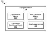
- FIG. 2is a schematic block diagram illustrating one embodiment of an apparatus 200 for increasing data protection in a data storage process in accordance with the present invention.
- the apparatus 200includes a data receiver module 202 , an ECC generation module 204 , a pre-storage consistency module 206 , and a data storage module 208 , which are described below. While the modules 202 - 208 are depicted in a storage controller, all or a portion of each module 202 - 208 may be located external to the storage controller 104 . For example, all or a portion of the modules 202 - 208 may be located in the data storage device 106 .
- the apparatus 200includes a data receiver module 202 that receives a storage block and existing parity information for the storage block.
- the storage blockincludes data that is intended to be stored together on the data storage device 106 .
- the storage blockmay be any convenient size for storing the data of the storage block.
- the storage blockfor example, may include data of a data packet that has been processed, encrypted, compressed, etc. and then divided into an appropriate size convenient for storage on the data storage device 106 .
- the storage blockmay include at least a portion of one or more data packets.
- a data packetmay include data from a file or object.
- the data from the file or objectmay be transmitted to the storage controller 104 as a data segment that may include complete file or object or a portion of the file or object.
- the storage controller 104may divide data of a data segment into data packets of a uniform size and adds a data packet header.
- the data packet headermay include one or more of a logical address of the file or object, an offset, and a data length.
- the storage controller 104receives a data segment over some type of transmission means such as a system bus (not shown) or computer network 112 (“network”).
- the data segmentis encoded using some error detection method such as 8b10b protection.
- parity bitsmay be generated in multiple dimensions to form the parity information.
- the parity informationcan then be used to check the data to determine if any bit errors exist.
- One of skill in the artwill recognize other ways to generate parity information and to use the parity information to check for bit errors in the data.
- the data receiver module 202receives existing parity information that was generated for the data of the storage block in a process prior to storing the data on the data storage device 106 .
- the apparatus 200includes an ECC generation module 204 that generates error correcting code (“ECC”) check bits for the data of the storage block in response to the data receiver module 202 receiving the storage block and the existing parity information.
- ECC check bits for the storage blockmay be generated by the ECC generation module 204 using a block code, such as a BCH code or Reed-Solomon Code, a convolutional code, such as a turbo code, or other standard code.
- the selected ECCtypically detects a certain number of bit errors and is capable of correcting a certain number of bit errors. For example, an ECC may detect five bit errors and may correct two bit errors.
- the ECC generation module 204generates ECC check bits that are stored with the data of the storage block so that when the storage block with the data and ECC check bits is later read, the ECC check bits can then be used to detect and correct bit errors that may have been introduced in the storage process, read process, or while the data is stored on the data storage device 106 .
- One of skill in the artwill recognize other error correcting codes and will understand how to implement an ECC to generate ECC check bits for a storage block.
- the apparatus 200includes a pre-storage consistency module 206 that uses the data of the storage block, the existing parity information, and the ECC check bits to determine if the data of the storage block, the existing parity information, and the ECC check bits are consistent.
- the pre-storage consistency module 206operates independently from the ECC generation module 204 providing redundancy in the error detection process.
- the pre-storage consistency module 206 and the ECC generation module 204are implemented with different logic hardware and/or different executable code so that an error in logic in the ECC does not cause the same error in the pre-storage consistency module 206 .
- this redundancyprovides a robust error detection capability that has no gaps in error detection and checks both data errors and logic errors.
- the apparatus 200include a data storage module 208 that stores the data of the storage block and the ECC check bits for the storage block on the data storage device 106 and the existing parity information for the storage block is not stored on the data storage device 106 .
- a data storage module 208that stores the data of the storage block and the ECC check bits for the storage block on the data storage device 106 and the existing parity information for the storage block is not stored on the data storage device 106 .
- the existing parity informationcan be dropped. Parity can then be regenerated when the data is read and the ECC check bits can be used to correct errors that may have occurred after the pre-storage consistency module 206 checks consistency of the data, existing parity, and ECC check bits.
- FIG. 3is a schematic block diagram illustrating one embodiment of another apparatus 300 for increasing data protection in a data storage process in accordance with the present invention.
- the apparatus 300includes a data receiver module 202 , an ECC generation module 204 , a pre-storage consistency module 206 , and a data storage module 208 , which are substantially similar to those described in relation to the apparatus 200 of FIG. 2 .
- the apparatus 300includes an ECC check bit parity module 302 , a data retriever module 304 , a parity generation module 306 , an ECC detection module 308 , a post-storage consistency module 310 , an ECC correction module 312 , an ECC syndrome parity module 314 , a pre-storage parity check module 316 , a post-retrieval parity check module 318 , and an overall consistency module 320 that includes a decoding module 322 , an encoding module 324 , and a parity consistency module 326 , which are described below.
- the modules 302 - 326are depicted in the storage controller 104 but all or a portion of each module 302 - 326 may be located external to the storage controller 104 , such as in the data storage device 106 or in a driver in a client 110 or server 108 .
- the pre-storage consistency module 206determines consistency using ECC parity information.
- the apparatus 300includes an ECC check bit parity module 302 that generates ECC parity information from the ECC check bits.
- the ECC check bit parity module 302generates ECC parity information by XORing the ECC check bits. Where the ECC check bits are a single column, the ECC parity information may be reduced to a single ECC parity bit that is the parity of the ECC check bits.
- the pre-storage consistency module 206determines if the ECC parity information is consistent with alternate parity information derived using independent logic from the data of the storage block and the existing parity information for the data.
- the pre-storage consistency module 206may determine if the ECC parity information is consistent with the alternate parity information by XORing the ECC parity information and the alternate parity information. Where there is a single ECC parity bit and the alternate parity information is a single bit, XORing the bits will typically represent a consistent result if the output of the XOR function is zero. If the output of the XOR function is a one, then the data, existing parity, and ECC check bits are not consistent and an error in at least one bit is present.
- FIGS. 4A and 4Bcollectively are an example 400 of determining if data, parity, and ECC are consistent in accordance with the present invention.
- the example 400depicts a simplified BCH(15,7,5) encoder and syndrome generation module.
- a 12 bit data blockis chosen comprising bits (d 0 -d 11 ) 402 in four rows and three columns.
- a parity bitis provided for each column (p 0 -p 2 ) 404 .
- the BCH encodergenerates 8 check bits, sufficient to correct 2 bit errors in the data block. While this may not be an especially attractive selection for a real world application, it enables sufficient explanation for one skilled in the art to extrapolate this to a larger and more sophisticated correction codes.
- the EncoderDataPrecalculator Modulecalculates nine intermediate solutions IS[0:8] for use as inputs d[0:8] to the Feedback Module, which are implemented in a pipeline fashion.
- the EncoderDataPrecalculator Module polynomialsare used to calculate IS[0:8].
- One column of data 402is input during a single clock cycle as i[0:3] with the input of the parity 404 as i[4].
- IS[8]is the parity of the intermediate solutions, IS[0:7].
- IS[8]is calculated using the data inputs i[0:3] and parity input i[4], not the intermediate solutions IS[0:7] or any subset of logic for any of the checkbit polynomials; this ensures that errors due to failures in the logic for IS[0:7] are not propagated to IS[8] and therefore undetectable.
- the polynomials for IS[0:7]have been obtained from generally available software.
- the polynomial for IS[8]is derived as follows:
- IS[8]is derived from the inputs i[0:4], not the intermediate solutions IS[0:7]. Additionally, the calculation for IS[8] includes as input the parity bit i[4], thus ensuring that the data protection is carried through this module and simultaneously ensuring that there is no shared logic that would negatively impact error detection.
- i[0:8]are initialized to zero and then the Intermediate Solutions, IS[0:8] from the EncoderDataPrecalculator Module are input one column at a time as d[0:8] as described above.
- i N+1 [0:8]o N [0:8].
- the polynomialis generated without use of the checkbit polynomials, and carries the parity information input as i[8] through to o[8]. To ensure this is the case, this logic must be synthesized in order to ensure the independence of the calculations in o[8] from those of o[0:7].
- the parity of each column of datais checked, in addition to checking that the parity o[8] matches a generated parity from the checkbits o[0:7].
- the decoder and syndrome moduleswork in the same way as encoding described above. This concludes the example 400 .
- the apparatus 300includes a data retriever module 304 , a parity generation module 306 , an ECC detection module 308 , a post-storage consistency module 310 , an ECC correction module 312 , and an ECC syndrome parity module 314 , which typically operate with regard to a read request and are described below.
- the data retriever module 304retrieves a storage block with data from one or more data packets stored on the data storage device 106 and ECC check bits for the storage block in response to a read request.
- the retrieved storage block and associated ECC check bitstypically were stored previously by the data storage module 208 after the ECC check bits were generated by the ECC generation module 204 and consistency checked by the pre-storage consistency module 206 .
- the parity generation module 306generates parity information for the data of the retrieved storage block and for the ECC check bits. Typically, the parity generation module 306 generates the parity information in the same form as the existing parity information that was dropped after the pre-storage consistency module 206 determines consistency. In addition, the parity generation module 306 generates parity for the ECC check bits.
- the ECC detection module 308uses the ECC check bits stored in conjunction with the storage block to generate an ECC syndrome to determine if the data of the retrieved storage block and the generated parity has an error.
- the apparatus 300typically includes an ECC correction module 312 that corrects one or more errors in the data of the storage block and updates one or more of parity bits in response to the ECC detection module 308 determining that the data of the retrieved storage block and the generated parity has an error.
- detection and correction of errorsis handled simultaneously using the generated ECC syndrome and a feedback function to iteratively detect and correct errors.
- the ECC check bitsare for the data of the storage block and do not include the parity bits. This is advantageous because if the ECC check bits are generated using both the data and the existing parity information, any error that occurs in the data will be reflected in the parity once the parity generation module 306 generates parity information after the storage block is read by the data retriever module 304 . If the ECC syndrome spans the data and the generated parity, one bit flip within the data will cause a change to the parity information so the ECC detection and correction modules 308 , 312 will have to use the syndrome to correct two bits; one in the data and then in the parity.
- the ECC generation module 204need not span the existing parity in addition to the data so that when the ECC detection module 308 generates the syndrome, the syndrome covers only the data and not the generated parity.
- the ECC correction module 308will typically regenerate the parity, at least for the column of the data with the corrected error.
- the present inventionmay include an embodiment where the ECC generation module 204 spans the existing parity along with the data.
- the post-storage consistency module 310uses the data from the retrieved storage block, the generated parity information generated by the parity generation module 306 , and the ECC syndrome to determine if the data, generated parity information, and the ECC syndrome are consistent.
- the post-storage consistency module 310is independent from the ECC detection and correction modules 308 , 312 . This redundancy provides a more robust error detection that helps to ensure data integrity as well as a check on the logic of the ECC and the post-storage consistency module 310 .
- the apparatus 300includes an ECC syndrome parity module 314 that uses the ECC syndrome to generate ECC syndrome parity information.
- the post-storage consistency module 310uses the ECC syndrome parity information to determine consistency. This is similar to the function of the ECC check bit parity module 302 and how the pre-storage consistency module 206 uses the ECC check bit parity information.
- the post-storage consistency module 310uses the data of the retrieved storage block and the generated parity information in a function independent from the ECC detection and correction modules 308 , 312 and the ECC syndrome parity module 314 to generate alternate parity information.
- the alternate parity informationis checked against the ECC syndrome parity information to determine consistency.
- the post-storage consistency module 310 and the ECC detection and correction modules 308 , 312use a process essentially similar to that described in the example depicted in FIG. 4 .
- the apparatus 300includes a pre-storage parity check module 316 that checks parity of the data of the storage block received by the data receiver module 202 using the existing parity information and the parity of the ECC check bits.
- the pre-storage parity check module 316checks parity prior to the data storage module 208 storing the storage block and ECC check bits.
- the pre-storage parity check module 316is typically another check that the received data does not have an error.
- Timing of the parity checkmay help to ensure no gap in error detection capability.
- the pre-storage parity check module 316may checks parity after the ECC generation module 204 has generated ECC check bits or as part of the ECC check bit generation process. By checking parity after or during the ECC check bit generation process, the pre-storage parity check module 316 helps to ensure that there have been no bit errors up to and including processing to generate ECC check bits where the data is then protected by the ECC check bits.
- the apparatus 300includes, in one embodiment, a post-retrieval parity check module 318 that checks parity of the retrieved storage block and the ECC check bits using the generated parity information from the retrieved storage block and ECC check bits after the ECC detection and correction modules 308 , 312 have completed determining if the data of the retrieved storage block has an error. Again, checking parity after ECC detection and correction typically ensures no gap in error detection capability.
- the apparatus 300includes an overall consistency module 320 that maintains protection of the data with no gap in error detection capability from receipt of the data by the system 100 until the data storage module 208 stores the data of the data segment.
- the overall consistency module 320typically includes a sub-module associated with each transition from one data protection scheme to another.
- the systemmay include the storage device 102 with the storage controller 104 and the data storage device 106 . The system 100 may then receive a data segment over a network 112 or a system bus (not shown).
- the data segmentwill be encoded to protect the data during transmission.
- the data segmentmay be protected using an 8b/10b protection scheme or similar data transmission protection scheme.
- the storage controller 104decodes the data and generates parity for the data.
- a portion of the overall consistency module 320ensures no gap in error detection capability through the decoding/parity generation processes.
- the overall consistency module 320may include a decoding module 322 that decodes data of the data segment, resulting in parity and un-encoded data of the data segment, in a single process step such that there is no gap in error detection capability from when the data is in an encoded form to when the data includes parity information.
- the decoding module 322includes a decoder that simultaneously generates parity so there is no gap in protection.
- the overall consistency module 320includes an encoding module 324 that encodes data of the data segment protected with parity information, resulting in encoded data of the data segment, in a single process step such that there is no gap in error detection capability from when the data includes parity information to when the data is in an encoded form.
- the parity generation module 306generates parity information for read data. After processing the data may then be transmitted to a requesting device such as the client 110 or server 108 . Typically the data is encoded and may be encoded again using an 8b/10b encoding scheme.
- the encoding module 324checks parity using the generated parity information and encodes the data in a single step so that there is no gap in error detection capability.
- the overall consistency module 320includes a parity consistency module 326 that maintains no gap in error detection capability by using parity information for the data of the data segment from when parity information is generated for the data of the data segment until the data receiver module 202 receives the existing parity information and the data in the form of the storage block.
- the parity consistency module 326maintains no gap in error detection capability from when the data retriever module 304 retrieves the storage block and the parity generation module 306 generates parity information for the data until the data protected using parity information is encoded by the encoding module 324 .
- the Parity Consistency Module 326maintains that there is no gap in data protection from the time the data is received and decoded by the Decoding Module 322 , through to storage in the Data Storage Device 106 , retrieval from the Data Storage Device 106 , and then transmitted by the Encoding Module 324 .
- the parity consistency module 326maintains parity through various processing steps such as encrypting the data, compressing the data, decrypting the data, decompressing the data, and/or a user-defined, application-specific function.
- the parity consistency module 326may work in conjunction with an encryption process so that there is no gap in protection during encryption.
- One of skill in the artwill recognize other processing steps where the parity consistency module 326 may maintain no gap in protection.
- the system 100may include a system bus, network 112 , or other devices and components.
- the overall consistency module 320may then include other decoding modules 322 , encoding modules 324 , modules similar to the parity consistency module 326 , or other modules and sub-modules to maintain consistency of protection such that there is no gap in error detection capability from a CPU or memory within the server 108 or other computer where the data segment is located, throughout processing and transmission, during storage, and throughout being read, processed, transmitted, etc. back to the CPU or memory.
- the CPU and/or memorymay include some error detection scheme and the overall consistency module 320 may maintain protection from inside the memory or CPU.
- One of skill in the artwill recognize other processes, devices, and components in the system 100 and modules or sub-modules that may work together with the overall consistency module 320 to ensure consistency such that there is no gap in error detection capability.
- FIG. 5is a schematic flow chart diagram illustrating one embodiment of a method 500 for increasing data protection while storing data in accordance with the present invention.
- the method 500begins and the data receiver module 202 receives 502 data in the form of a storage block and associated existing parity information.
- the ECC generation module 204generates 504 ECC check bits for the data of the storage block.
- the ECC check bitsare generated using a standard code such as a block code or convolutional code.
- the pre-storage consistency module 206uses 506 the data of the storage block, the existing parity information, and the ECC check bits to determine if the data of the storage block, the existing parity information, and the ECC check bits are consistent.
- the ECC check bit parity module 302generates ECC check bit parity information and an independent logic uses the data and existing parity information to generate alternate parity information that is checked against the ECC check bit parity information.
- the data storage module 208stores 510 the data as a storage block along with the ECC check bits. The existing parity information is dropped and not stored. If the pre-storage consistency module 206 determines 508 that the data, existing parity and ECC check bits are not consistent, the pre-storage consistency module 206 generates 512 an appropriate error and the method 500 ends. The storage controller 104 typically then takes appropriate action to correct the error or fail the storage request.
- FIG. 6is a schematic flow chart diagram illustrating one embodiment of a method 600 for increasing data protection from receipt of the data to storage of the data in accordance with the present invention.
- the method 600is for a system 100 that includes a storage device 102 with a storage controller 104 and a data storage device 106 .
- the method 600begins and the decode module 322 decodes 602 data of a data segment and generates parity information for the data such that there is no gap in error detection capability.
- the storage controller 104processes the data and the parity consistency module 326 maintains 604 parity protection such that there is no gap in parity protection for the data through encryption, compression, etc. until the data and existing parity are received by the data receiver module 202 .
- the data receiver module 202receives 606 the data and existing parity information and the ECC generation module 204 generates 608 ECC check bits for the data using a standard code such as a block code, a convolutional code, etc.
- the pre-storage consistency module 206uses 610 the data, ECC check bits, and existing parity information to determine consistency. If the data, parity information, and ECC check bits are consistent, the data storage module 208 stores 612 the data and ECC check bits on the data storage device 106 without storing the existing parity information and the method 600 ends.
- the storage controller 104any errors detecting during decoding, processing, generation of the ECC check bits, etc. will be handled appropriately by the storage controller 104 .
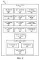
- FIG. 7is a schematic flow chart diagram illustrating one embodiment of a method 700 for increasing data protection from retrieval of data to delivering the data in accordance with the present invention.
- the method 700is for a system 100 that includes a storage device 102 with a storage controller 104 and a data storage device 106 .
- the method 700begins and the data retriever module 304 retrieves 702 a storage block stored on the data storage device 106 and ECC check bits for the storage block in response to a read request.
- the parity generation module 306generates 704 parity information for the data of the retrieved storage block and for the ECC check bits.
- the ECC detection module 308generates 706 an ECC syndrome using the data of the retrieved storage block and the corresponding ECC check bits and determines if there are one or more errors in the data.
- the ECC correction module 312typically works with the ECC detection module 308 to iteratively detect and correct errors.
- the post-storage consistency module 310uses 708 the ECC check bits, the generated parity information, and the ECC syndrome to determine if the data, parity, and ECC syndrome are consistent. If not, the storage controller 104 takes appropriate action or the ECC detection and correction modules 308 , 312 continue to iterate to correct the errors.
- the storage controller 104processes the read data and the parity consistency module 326 maintains 710 parity protection while the data is decrypted, decompressed, etc.
- the encoding module 324encodes 712 the data and checks parity in a single step so that there is no gap in error detection capability and the method 700 ends. Again, any errors detected through parity checks, ECC error detection, etc. are handled appropriately by the storage controller 104 .
Landscapes
- Engineering & Computer Science (AREA)
- Theoretical Computer Science (AREA)
- Physics & Mathematics (AREA)
- General Engineering & Computer Science (AREA)
- General Physics & Mathematics (AREA)
- Human Computer Interaction (AREA)
- Software Systems (AREA)
- Computer Security & Cryptography (AREA)
- Quality & Reliability (AREA)
- Microelectronics & Electronic Packaging (AREA)
- Detection And Correction Of Errors (AREA)
Abstract
Description
- 1. Each of the polynomials for IS[0:8] in the EncoderPreCalcData Module are repeated in tabular form in rows2-9 and
row 13, respectively in Table 1 inFIG. 4A . The polynomials for IS[0:7] are XORed together (row10). Since the XOR of the results of the polynomials is equal to the result of the XOR of the polynomials, this enables an independent calculation of the parity of the intermediate solutions. In Table 1, “1's” are placed in the cells of the table when the coefficients of the polynomials are “1,” and left blank when the coefficients are “0.” For example, the coefficient for i[0] in the XOR(IS[0:7]) polynomial (row10) is “0” because i[0] is used in an even number polynomials (e.g. the polynomials corresponding to IS[0,4,6,7]), and i[0] XORed with itself four times is “0”. The coefficient i[2] for the XOR(IS[0:7]) is “1” because i[2] is used in an odd number of polynomials (e.g. the polynomials corresponding to IS[1,2,5,6,7]). Note that the parity of the column of input data, i[4], is not included in this calculation. - 2. The Parity_1apolynomial (row11) contains only i[4] as an input, the identity function for i[4]. The Parity_2apolynomial (row12) has inputs i[0:3], which is the same function that i[4] was created from originally (not shown). Since Parity—1a=Parity—2a, XOR(Parity—1a,Parity—2a)=0. The Parity_1aand Parity_2apolynomials are therefore XORed with the XOR(IS[0:7]) polynomial (row10), resulting in IS[8] (row13). This is equivalent to inverting the coefficients of the XOR(IS[0:7]) polynomial (row10).
- 1. Each of the polynomials for IS[0:8] in the EncoderPreCalcData Module are repeated in tabular form in rows2-9 and
Claims (27)
Priority Applications (4)
| Application Number | Priority Date | Filing Date | Title |
|---|---|---|---|
| US12/098,427US8316277B2 (en) | 2007-12-06 | 2008-04-05 | Apparatus, system, and method for ensuring data validity in a data storage process |
| CN200980121155.8ACN102084343A (en) | 2008-04-05 | 2009-04-04 | A device, system and method for ensuring data validity during data storage |
| JP2011503238AJP2011516984A (en) | 2008-04-05 | 2009-04-04 | Apparatus, system and method for ensuring data validity in a data storage process |
| PCT/US2009/039572WO2009124304A1 (en) | 2008-04-05 | 2009-04-04 | Apparatus, system, and method for ensuring data validity in a data storage process |
Applications Claiming Priority (2)
| Application Number | Priority Date | Filing Date | Title |
|---|---|---|---|
| US11/952,091US8266496B2 (en) | 2006-12-06 | 2007-12-06 | Apparatus, system, and method for managing data using a data pipeline |
| US12/098,427US8316277B2 (en) | 2007-12-06 | 2008-04-05 | Apparatus, system, and method for ensuring data validity in a data storage process |
Related Parent Applications (1)
| Application Number | Title | Priority Date | Filing Date |
|---|---|---|---|
| US11/952,091Continuation-In-PartUS8266496B2 (en) | 2006-12-06 | 2007-12-06 | Apparatus, system, and method for managing data using a data pipeline |
Publications (2)
| Publication Number | Publication Date |
|---|---|
| US20090150744A1 US20090150744A1 (en) | 2009-06-11 |
| US8316277B2true US8316277B2 (en) | 2012-11-20 |
Family
ID=40722938
Family Applications (1)
| Application Number | Title | Priority Date | Filing Date |
|---|---|---|---|
| US12/098,427Active2030-09-16US8316277B2 (en) | 2007-12-06 | 2008-04-05 | Apparatus, system, and method for ensuring data validity in a data storage process |
Country Status (4)
| Country | Link |
|---|---|
| US (1) | US8316277B2 (en) |
| JP (1) | JP2011516984A (en) |
| CN (1) | CN102084343A (en) |
| WO (1) | WO2009124304A1 (en) |
Cited By (8)
| Publication number | Priority date | Publication date | Assignee | Title |
|---|---|---|---|---|
| US20120198312A1 (en)* | 2011-02-02 | 2012-08-02 | Seagate Technology Llc | Methods and devices to increase memory device data reliability |
| US9032269B2 (en) | 2011-07-22 | 2015-05-12 | Sandisk Technologies Inc. | Systems and methods of storing data |
| US9329926B1 (en) | 2013-09-13 | 2016-05-03 | Microsemi Storage Solutions (U.S.), Inc. | Overlapping data integrity for semiconductor devices |
| US9342518B1 (en)* | 2012-06-21 | 2016-05-17 | Emc Corporation | Declaring directives in a data store |
| US11362678B2 (en) | 2011-12-30 | 2022-06-14 | Streamscale, Inc. | Accelerated erasure coding system and method |
| US11500723B2 (en) | 2011-12-30 | 2022-11-15 | Streamscale, Inc. | Using parity data for concurrent data authentication, correction, compression, and encryption |
| US11586560B2 (en)* | 2016-12-27 | 2023-02-21 | Intel Corporation | Secure memory |
| US11886295B2 (en) | 2022-01-31 | 2024-01-30 | Pure Storage, Inc. | Intra-block error correction |
Families Citing this family (20)
| Publication number | Priority date | Publication date | Assignee | Title |
|---|---|---|---|---|
| JP4865016B2 (en)* | 2009-08-27 | 2012-02-01 | 株式会社東芝 | Processor |
| JP2011108306A (en)* | 2009-11-16 | 2011-06-02 | Sony Corp | Nonvolatile memory and memory system |
| US8850114B2 (en) | 2010-09-07 | 2014-09-30 | Daniel L Rosenband | Storage array controller for flash-based storage devices |
| US20120324143A1 (en) | 2011-06-15 | 2012-12-20 | Data Design Corporation | Methods and apparatus for data access by a reprogrammable circuit module |
| US9417894B1 (en) | 2011-06-15 | 2016-08-16 | Ryft Systems, Inc. | Methods and apparatus for a tablet computer system incorporating a reprogrammable circuit module |
| GB201114831D0 (en)* | 2011-08-26 | 2011-10-12 | Univ Oxford Brookes | Circuit with error correction |
| US9054840B2 (en)* | 2011-12-15 | 2015-06-09 | Lenovo Enterprise Solutions (Singapore) Pte. Ltd. | Error detection and correction of a data transmission |
| CN102567132B (en)* | 2011-12-30 | 2014-12-03 | 记忆科技(深圳)有限公司 | End-to-end chip data path protection device and method for the same |
| US8984373B2 (en)* | 2012-02-22 | 2015-03-17 | Silicon Motion, Inc. | Method for accessing flash memory and associated flash memory controller |
| KR102081980B1 (en)* | 2012-10-08 | 2020-02-27 | 삼성전자 주식회사 | Method for performing write operation or read operation in memory system |
| JP6212396B2 (en)* | 2014-01-08 | 2017-10-11 | ルネサスエレクトロニクス株式会社 | Data processing device |
| US20150311921A1 (en)* | 2014-04-25 | 2015-10-29 | Kabushiki Kaisha Toshiba | Memory controller, storage device and decoding method |
| US20160077959A1 (en)* | 2014-09-12 | 2016-03-17 | Qualcomm Incorporated | System and Method for Sharing a Solid-State Non-Volatile Memory Resource |
| US9530442B1 (en)* | 2015-09-23 | 2016-12-27 | Western Digital Technologies, Inc. | Enhanced low overhead data protection in data storage drives |
| CN106802837B (en)* | 2015-11-26 | 2020-02-21 | 华为技术有限公司 | A method and apparatus for updating error detection and correction ECC code |
| US10284230B2 (en)* | 2016-11-15 | 2019-05-07 | Western Digital Technologies, Inc. | Linked storage system and host system error correcting code |
| CN111062185A (en)* | 2019-11-27 | 2020-04-24 | 深圳壹账通智能科技有限公司 | External verification method and device for data format, computer equipment and storage medium |
| US11757472B1 (en)* | 2022-05-16 | 2023-09-12 | Seagate Technology Llc | Coarse interleaving |
| US11960397B2 (en)* | 2022-06-16 | 2024-04-16 | Western Digital Technologies, Inc. | Data mapping comparison for improved synchronization in data storage devices |
| CN117093411A (en)* | 2023-09-25 | 2023-11-21 | 北京地平线信息技术有限公司 | Data protection method and device, storage medium and electronic equipment |
Citations (120)
| Publication number | Priority date | Publication date | Assignee | Title |
|---|---|---|---|---|
| US5151905A (en) | 1988-10-14 | 1992-09-29 | Sony Corporation | Data recording method |
| US5261068A (en) | 1990-05-25 | 1993-11-09 | Dell Usa L.P. | Dual path memory retrieval system for an interleaved dynamic RAM memory unit |
| US5291496A (en) | 1990-10-18 | 1994-03-01 | The United States Of America As Represented By The United States Department Of Energy | Fault-tolerant corrector/detector chip for high-speed data processing |
| US5313475A (en) | 1991-10-31 | 1994-05-17 | International Business Machines Corporation | ECC function with self-contained high performance partial write or read/modify/write and parity look-ahead interface scheme |
| US5325509A (en) | 1991-03-05 | 1994-06-28 | Zitel Corporation | Method of operating a cache memory including determining desirability of cache ahead or cache behind based on a number of available I/O operations |
| US5404485A (en) | 1993-03-08 | 1995-04-04 | M-Systems Flash Disk Pioneers Ltd. | Flash file system |
| US5438671A (en) | 1991-07-19 | 1995-08-01 | Dell U.S.A., L.P. | Method and system for transferring compressed bytes of information between separate hard disk drive units |
| US5504882A (en) | 1994-06-20 | 1996-04-02 | International Business Machines Corporation | Fault tolerant data storage subsystem employing hierarchically arranged controllers |
| US5559988A (en) | 1993-12-30 | 1996-09-24 | Intel Corporation | Method and circuitry for queuing snooping, prioritizing and suspending commands |
| US5594883A (en) | 1993-04-14 | 1997-01-14 | International Business Machines Corporation | Hierarchical data storage system employing contemporaneous transfer of designated data pages to long write and short read cycle memory |
| US5603001A (en) | 1994-05-09 | 1997-02-11 | Kabushiki Kaisha Toshiba | Semiconductor disk system having a plurality of flash memories |
| US5701434A (en) | 1995-03-16 | 1997-12-23 | Hitachi, Ltd. | Interleave memory controller with a common access queue |
| US5754563A (en) | 1995-09-11 | 1998-05-19 | Ecc Technologies, Inc. | Byte-parallel system for implementing reed-solomon error-correcting codes |
| US5845313A (en) | 1995-07-31 | 1998-12-01 | Lexar | Direct logical block addressing flash memory mass storage architecture |
| US5845329A (en) | 1993-01-29 | 1998-12-01 | Sanyo Electric Co., Ltd. | Parallel computer |
| US5907856A (en) | 1995-07-31 | 1999-05-25 | Lexar Media, Inc. | Moving sectors within a block of information in a flash memory mass storage architecture |
| US5930815A (en) | 1995-07-31 | 1999-07-27 | Lexar Media, Inc. | Moving sequential sectors within a block of information in a flash memory mass storage architecture |
| US5960462A (en) | 1996-09-26 | 1999-09-28 | Intel Corporation | Method and apparatus for analyzing a main memory configuration to program a memory controller |
| US5961660A (en) | 1997-03-03 | 1999-10-05 | International Business Machines Corporation | Method and apparatus for optimizing ECC memory performance |
| US5969986A (en) | 1998-06-23 | 1999-10-19 | Invox Technology | High-bandwidth read and write architectures for non-volatile memories |
| US6000019A (en) | 1995-06-06 | 1999-12-07 | Hewlett-Packard Company | SDRAM data allocation system and method utilizing dual bank storage and retrieval |
| US6105076A (en) | 1999-04-23 | 2000-08-15 | International Business Machines Corporation | Method, system, and program for performing data transfer operations on user data |
| US6128695A (en) | 1995-07-31 | 2000-10-03 | Lexar Media, Inc. | Identification and verification of a sector within a block of mass storage flash memory |
| US6141249A (en) | 1999-04-01 | 2000-10-31 | Lexar Media, Inc. | Organization of blocks within a nonvolatile memory unit to effectively decrease sector write operation time |
| US6170047B1 (en) | 1994-11-16 | 2001-01-02 | Interactive Silicon, Inc. | System and method for managing system memory and/or non-volatile memory using a memory controller with integrated compression and decompression capabilities |
| US6170039B1 (en) | 1997-05-16 | 2001-01-02 | Nec Corporation | Memory controller for interchanging memory against memory error in interleave memory system |
| US6172906B1 (en) | 1995-07-31 | 2001-01-09 | Lexar Media, Inc. | Increasing the memory performance of flash memory devices by writing sectors simultaneously to multiple flash memory devices |
| US6173381B1 (en) | 1994-11-16 | 2001-01-09 | Interactive Silicon, Inc. | Memory controller including embedded data compression and decompression engines |
| US6185654B1 (en) | 1998-07-17 | 2001-02-06 | Compaq Computer Corporation | Phantom resource memory address mapping system |
| US6240040B1 (en) | 2000-03-15 | 2001-05-29 | Advanced Micro Devices, Inc. | Multiple bank simultaneous operation for a flash memory |
| GB0123416D0 (en) | 2001-09-28 | 2001-11-21 | Memquest Ltd | Non-volatile memory control |
| US6330688B1 (en) | 1995-10-31 | 2001-12-11 | Intel Corporation | On chip error correction for devices in a solid state drive |
| US6385710B1 (en) | 1996-02-23 | 2002-05-07 | Sun Microsystems, Inc. | Multiple-mode external cache subsystem |
| US20020069318A1 (en) | 2000-12-01 | 2002-06-06 | Chow Yan Chiew | Real time application accelerator and method of operating the same |
| US6404647B1 (en) | 2000-08-24 | 2002-06-11 | Hewlett-Packard Co. | Solid-state mass memory storage device |
| US6412080B1 (en) | 1999-02-23 | 2002-06-25 | Microsoft Corporation | Lightweight persistent storage system for flash memory devices |
| US6418478B1 (en) | 1997-10-30 | 2002-07-09 | Commvault Systems, Inc. | Pipelined high speed data transfer mechanism |
| US20020194451A1 (en) | 2001-06-19 | 2002-12-19 | Tdk Corporation | Memory controller, flash memory system employing memory controller and method for controlling flash memory device |
| US6523102B1 (en) | 2000-04-14 | 2003-02-18 | Interactive Silicon, Inc. | Parallel compression/decompression system and method for implementation of in-memory compressed cache improving storage density and access speed for industry standard memory subsystems and in-line memory modules |
| US20030061296A1 (en) | 2001-09-24 | 2003-03-27 | International Business Machines Corporation | Memory semantic storage I/O |
| US20030093741A1 (en) | 2001-11-14 | 2003-05-15 | Cenk Argon | Parallel decoder for product codes |
| US6587915B1 (en) | 1999-09-29 | 2003-07-01 | Samsung Electronics Co., Ltd. | Flash memory having data blocks, spare blocks, a map block and a header block and a method for controlling the same |
| US6601211B1 (en) | 1996-10-15 | 2003-07-29 | Micron Technology, Inc. | Write reduction in flash memory systems through ECC usage |
| US6625685B1 (en) | 2000-09-20 | 2003-09-23 | Broadcom Corporation | Memory controller with programmable configuration |
| US20030198084A1 (en) | 2002-04-18 | 2003-10-23 | Hitachi, Ltd. | Nonvolatile semiconductor memory |
| US6671757B1 (en) | 2000-01-26 | 2003-12-30 | Fusionone, Inc. | Data transfer and synchronization system |
| US6675349B1 (en) | 2000-05-11 | 2004-01-06 | International Business Machines Corporation | Error correction coding of data blocks with included parity bits |
| US6715046B1 (en) | 2001-11-29 | 2004-03-30 | Cisco Technology, Inc. | Method and apparatus for reading from and writing to storage using acknowledged phases of sets of data |
| US6728851B1 (en) | 1995-07-31 | 2004-04-27 | Lexar Media, Inc. | Increasing the memory performance of flash memory devices by writing sectors simultaneously to multiple flash memory devices |
| US6754774B2 (en) | 2001-07-06 | 2004-06-22 | Juniper Networks, Inc. | Streaming output engine facilitating data transfers between application engines and memory |
| US6757800B1 (en) | 1995-07-31 | 2004-06-29 | Lexar Media, Inc. | Increasing the memory performance of flash memory devices by writing sectors simultaneously to multiple flash memory devices |
| US6779088B1 (en) | 2000-10-24 | 2004-08-17 | International Business Machines Corporation | Virtual uncompressed cache size control in compressed memory systems |
| US6785785B2 (en) | 2000-01-25 | 2004-08-31 | Hewlett-Packard Development Company, L.P. | Method for supporting multi-level stripping of non-homogeneous memory to maximize concurrency |
| US20040186946A1 (en) | 2003-03-19 | 2004-09-23 | Jinaeon Lee | Flash file system |
| US6801979B1 (en) | 1995-07-31 | 2004-10-05 | Lexar Media, Inc. | Method and apparatus for memory control circuit |
| US20040268359A1 (en) | 2003-06-27 | 2004-12-30 | Hanes David H. | Computer-readable medium, method and computer system for processing input/output requests |
| US20050002263A1 (en) | 2003-05-20 | 2005-01-06 | Yasuaki Iwase | Writing control method and writing control system of semiconductor storage device, and portable electronic apparatus |
| US20050015539A1 (en) | 2002-01-09 | 2005-01-20 | Takashi Horii | Memory system and memory card |
| US20050055497A1 (en) | 1995-07-31 | 2005-03-10 | Petro Estakhri | Faster write operations to nonvolatile memory by manipulation of frequently-accessed sectors |
| US6871257B2 (en) | 2002-02-22 | 2005-03-22 | Sandisk Corporation | Pipelined parallel programming operation in a non-volatile memory system |
| US6883079B1 (en) | 2000-09-01 | 2005-04-19 | Maxtor Corporation | Method and apparatus for using data compression as a means of increasing buffer bandwidth |
| US20050132259A1 (en) | 2003-12-12 | 2005-06-16 | Emmot Darel N. | Error correction method and system |
| US20050132148A1 (en) | 2003-12-10 | 2005-06-16 | International Business Machines Corp. | Method and system for thread-based memory speculation in a memory subsystem of a data processing system |
| US6910170B2 (en) | 2001-01-08 | 2005-06-21 | Samsung Electronics Co., Ltd. | Pre-decoder for a turbo decoder, for recovering punctured parity symbols, and a method for recovering a turbo code |
| US20050144361A1 (en) | 2003-12-30 | 2005-06-30 | Gonzalez Carlos J. | Adaptive mode switching of flash memory address mapping based on host usage characteristics |
| US20050149819A1 (en) | 2003-12-15 | 2005-07-07 | Daewoo Electronics Corporation | Three-dimensional error correction method |
| US20050149618A1 (en) | 2003-12-23 | 2005-07-07 | Mobile Action Technology Inc. | System and method of transmitting electronic files over to a mobile phone |
| US6938133B2 (en) | 2001-09-28 | 2005-08-30 | Hewlett-Packard Development Company, L.P. | Memory latency and bandwidth optimizations |
| US20050229090A1 (en) | 2004-04-05 | 2005-10-13 | Ba-Zhong Shen | LDPC (Low Density Parity Check) coded signal decoding using parallel and simultaneous bit node and check node processing |
| US20050240713A1 (en) | 2004-04-22 | 2005-10-27 | V-Da Technology | Flash memory device with ATA/ATAPI/SCSI or proprietary programming interface on PCI express |
| US20050246510A1 (en) | 2003-11-13 | 2005-11-03 | Retnamma Manoj V | System and method for combining data streams in pipelined storage operations in a storage network |
| US6978342B1 (en) | 1995-07-31 | 2005-12-20 | Lexar Media, Inc. | Moving sectors within a block of information in a flash memory mass storage architecture |
| US6977599B2 (en) | 2001-05-08 | 2005-12-20 | International Business Machines Corporation | 8B/10B encoding and decoding for high speed applications |
| US20060004955A1 (en) | 2002-06-20 | 2006-01-05 | Rambus Inc. | Dynamic memory supporting simultaneous refresh and data-access transactions |
| US6996676B2 (en) | 2002-11-14 | 2006-02-07 | International Business Machines Corporation | System and method for implementing an adaptive replacement cache policy |
| US7000063B2 (en) | 2001-10-05 | 2006-02-14 | Matrix Semiconductor, Inc. | Write-many memory device and method for limiting a number of writes to the write-many memory device |
| US7010662B2 (en) | 2002-02-27 | 2006-03-07 | Microsoft Corporation | Dynamic data structures for tracking file system free space in a flash memory device |
| US20060059326A1 (en) | 2002-11-21 | 2006-03-16 | Microsoft Corporation | Dynamic data structures for tracking file system free space in a flash memory device |
| US20060075057A1 (en) | 2004-08-30 | 2006-04-06 | International Business Machines Corporation | Remote direct memory access system and method |
| US20060107097A1 (en) | 2004-10-22 | 2006-05-18 | Ofir Zohar | Data protection in a mass storage system |
| US7058769B1 (en) | 2002-08-07 | 2006-06-06 | Nvidia Corporation | Method and system of improving disk access time by compression |
| US7076723B2 (en) | 2003-03-14 | 2006-07-11 | Quantum Corporation | Error correction codes |
| US20060152981A1 (en) | 2005-01-11 | 2006-07-13 | Ryu Dong-Ryul | Solid state disk controller apparatus |
| US7082495B2 (en) | 2002-06-27 | 2006-07-25 | Microsoft Corporation | Method and apparatus to reduce power consumption and improve read/write performance of hard disk drives using non-volatile memory |
| US7085879B2 (en) | 2002-02-27 | 2006-08-01 | Microsoft Corporation | Dynamic data structures for tracking data stored in a flash memory device |
| US7089391B2 (en) | 2000-04-14 | 2006-08-08 | Quickshift, Inc. | Managing a codec engine for memory compression/decompression operations using a data movement engine |
| US7096321B2 (en) | 2003-10-21 | 2006-08-22 | International Business Machines Corporation | Method and system for a cache replacement technique with adaptive skipping |
| US20060248387A1 (en) | 2005-04-15 | 2006-11-02 | Microsoft Corporation | In-line non volatile memory disk read cache and write buffer |
| US7149947B1 (en) | 2003-09-04 | 2006-12-12 | Emc Corporation | Method of and system for validating an error correction code and parity information associated with a data word |
| US20070016699A1 (en) | 2005-07-14 | 2007-01-18 | Canon Kabushiki Kaisha | Memory control apparatus and method |
| US7178081B2 (en) | 2002-12-24 | 2007-02-13 | Electronics And Telecommunications Research Institute | Simplified message-passing decoder for low-density parity-check codes |
| US7181572B2 (en) | 2002-12-02 | 2007-02-20 | Silverbrook Research Pty Ltd | Cache updating method and apparatus |
| US20070050571A1 (en) | 2005-09-01 | 2007-03-01 | Shuji Nakamura | Storage system, storage device, and control method thereof |
| US20070074092A1 (en)* | 2005-09-23 | 2007-03-29 | Intel Corporation | Techniques to determine integrity of information |
| US20070086260A1 (en) | 2005-10-13 | 2007-04-19 | Sinclair Alan W | Method of storing transformed units of data in a memory system having fixed sized storage blocks |
| US7219238B2 (en) | 2002-03-20 | 2007-05-15 | Seiko Epson Corporation | Data transfer control device, electronic instrument, and data transfer control method |
| US7243203B2 (en) | 2003-06-13 | 2007-07-10 | Sandisk 3D Llc | Pipeline circuit for low latency memory |
| US20070162830A1 (en) | 2002-01-21 | 2007-07-12 | Koninklijke Philips Electronics, N.V. | Method of encoding and decoding |
| US7246179B2 (en) | 2000-10-17 | 2007-07-17 | Microsoft Corporation | System and method for controlling mass storage class digital imaging devices |
| US20070204197A1 (en) | 2005-12-20 | 2007-08-30 | Takashi Yokokawa | Decoding device, control method, and program |
| US20070204199A1 (en)* | 2006-02-13 | 2007-08-30 | Samsung Electronics Co., Ltd. | Semiconductor memory device and memory system including the same |
| US20070233937A1 (en) | 2006-03-31 | 2007-10-04 | Coulson Richard L | Reliability of write operations to a non-volatile memory |
| US20070245217A1 (en) | 2006-03-28 | 2007-10-18 | Stmicroelectronics S.R.L. | Low-density parity check decoding |
| US20070271572A1 (en) | 1998-12-18 | 2007-11-22 | Emc Corporation | Messaging mechanism for inter processor communication |
| US20070271468A1 (en) | 2006-05-05 | 2007-11-22 | Mckenney Paul E | Method and Apparatus for Maintaining Data Integrity When Switching Between Different Data Protection Methods |
| US7305520B2 (en) | 2004-01-30 | 2007-12-04 | Hewlett-Packard Development Company, L.P. | Storage system with capability to allocate virtual storage segments among a plurality of controllers |
| US20070300008A1 (en) | 2006-06-23 | 2007-12-27 | Microsoft Corporation | Flash management techniques |
| US20080022187A1 (en)* | 2006-06-30 | 2008-01-24 | Intel Corporation | Memory device that reflects back error detection signals |
| US7340566B2 (en) | 2002-10-21 | 2008-03-04 | Microsoft Corporation | System and method for initializing a memory device from block oriented NAND flash |
| US20080141043A1 (en) | 2006-12-06 | 2008-06-12 | David Flynn | Apparatus, system, and method for managing data using a data pipeline |
| US7450420B2 (en) | 2005-08-03 | 2008-11-11 | Sandisk Corporation | Reclaiming data storage capacity in flash memories |
| US7480766B2 (en) | 2005-08-03 | 2009-01-20 | Sandisk Corporation | Interfacing systems operating through a logical address space and on a direct data file basis |
| US7487320B2 (en) | 2004-12-15 | 2009-02-03 | International Business Machines Corporation | Apparatus and system for dynamically allocating main memory among a plurality of applications |
| US20090083485A1 (en) | 2007-09-25 | 2009-03-26 | Cheng Steven S | Nonvolatile memory with self recovery |
| US7516267B2 (en) | 2005-11-03 | 2009-04-07 | Intel Corporation | Recovering from a non-volatile memory failure |
| US7552271B2 (en) | 2005-08-03 | 2009-06-23 | Sandisk Corporation | Nonvolatile memory with block management |
| US7644239B2 (en) | 2004-05-03 | 2010-01-05 | Microsoft Corporation | Non-volatile memory cache performance improvement |
| US20100091535A1 (en) | 2007-03-12 | 2010-04-15 | Anobit Technologies Ltd | Adaptive estimation of memory cell read thresholds |
| US7725628B1 (en) | 2004-04-20 | 2010-05-25 | Lexar Media, Inc. | Direct secondary device interface by a host |
| US20110182119A1 (en) | 2010-01-27 | 2011-07-28 | Fusion-Io, Inc. | Apparatus, system, and method for determining a read voltage threshold for solid-state storage media |
- 2008
- 2008-04-05USUS12/098,427patent/US8316277B2/enactiveActive
- 2009
- 2009-04-04CNCN200980121155.8Apatent/CN102084343A/enactivePending
- 2009-04-04WOPCT/US2009/039572patent/WO2009124304A1/enactiveApplication Filing
- 2009-04-04JPJP2011503238Apatent/JP2011516984A/ennot_activeWithdrawn
Patent Citations (158)
| Publication number | Priority date | Publication date | Assignee | Title |
|---|---|---|---|---|
| US5151905A (en) | 1988-10-14 | 1992-09-29 | Sony Corporation | Data recording method |
| US5261068A (en) | 1990-05-25 | 1993-11-09 | Dell Usa L.P. | Dual path memory retrieval system for an interleaved dynamic RAM memory unit |
| US5291496A (en) | 1990-10-18 | 1994-03-01 | The United States Of America As Represented By The United States Department Of Energy | Fault-tolerant corrector/detector chip for high-speed data processing |
| US5325509A (en) | 1991-03-05 | 1994-06-28 | Zitel Corporation | Method of operating a cache memory including determining desirability of cache ahead or cache behind based on a number of available I/O operations |
| US5438671A (en) | 1991-07-19 | 1995-08-01 | Dell U.S.A., L.P. | Method and system for transferring compressed bytes of information between separate hard disk drive units |
| US5313475A (en) | 1991-10-31 | 1994-05-17 | International Business Machines Corporation | ECC function with self-contained high performance partial write or read/modify/write and parity look-ahead interface scheme |
| US5845329A (en) | 1993-01-29 | 1998-12-01 | Sanyo Electric Co., Ltd. | Parallel computer |
| US5404485A (en) | 1993-03-08 | 1995-04-04 | M-Systems Flash Disk Pioneers Ltd. | Flash file system |
| US5594883A (en) | 1993-04-14 | 1997-01-14 | International Business Machines Corporation | Hierarchical data storage system employing contemporaneous transfer of designated data pages to long write and short read cycle memory |
| US5559988A (en) | 1993-12-30 | 1996-09-24 | Intel Corporation | Method and circuitry for queuing snooping, prioritizing and suspending commands |
| US5603001A (en) | 1994-05-09 | 1997-02-11 | Kabushiki Kaisha Toshiba | Semiconductor disk system having a plurality of flash memories |
| US5504882A (en) | 1994-06-20 | 1996-04-02 | International Business Machines Corporation | Fault tolerant data storage subsystem employing hierarchically arranged controllers |
| US6370631B1 (en) | 1994-11-16 | 2002-04-09 | Interactive Silicon, Inc. | Memory controller including compression/decompression capabilities for improved data access |
| US6173381B1 (en) | 1994-11-16 | 2001-01-09 | Interactive Silicon, Inc. | Memory controller including embedded data compression and decompression engines |
| US6170047B1 (en) | 1994-11-16 | 2001-01-02 | Interactive Silicon, Inc. | System and method for managing system memory and/or non-volatile memory using a memory controller with integrated compression and decompression capabilities |
| US5701434A (en) | 1995-03-16 | 1997-12-23 | Hitachi, Ltd. | Interleave memory controller with a common access queue |
| US6000019A (en) | 1995-06-06 | 1999-12-07 | Hewlett-Packard Company | SDRAM data allocation system and method utilizing dual bank storage and retrieval |
| US20090204750A1 (en) | 1995-07-31 | 2009-08-13 | Petro Estakhri | Direct logical block addressing flash memory mass storage architecture |
| US6393513B2 (en) | 1995-07-31 | 2002-05-21 | Lexar Media, Inc. | Identification and verification of a sector within a block of mass storage flash memory |
| US20050055497A1 (en) | 1995-07-31 | 2005-03-10 | Petro Estakhri | Faster write operations to nonvolatile memory by manipulation of frequently-accessed sectors |
| US6912618B2 (en) | 1995-07-31 | 2005-06-28 | Lexar Media, Inc. | Direct logical block addressing flash memory mass storage architecture |
| US5930815A (en) | 1995-07-31 | 1999-07-27 | Lexar Media, Inc. | Moving sequential sectors within a block of information in a flash memory mass storage architecture |
| US5907856A (en) | 1995-07-31 | 1999-05-25 | Lexar Media, Inc. | Moving sectors within a block of information in a flash memory mass storage architecture |
| US6128695A (en) | 1995-07-31 | 2000-10-03 | Lexar Media, Inc. | Identification and verification of a sector within a block of mass storage flash memory |
| US6801979B1 (en) | 1995-07-31 | 2004-10-05 | Lexar Media, Inc. | Method and apparatus for memory control circuit |
| US6145051A (en) | 1995-07-31 | 2000-11-07 | Lexar Media, Inc. | Moving sectors within a block of information in a flash memory mass storage architecture |
| US5845313A (en) | 1995-07-31 | 1998-12-01 | Lexar | Direct logical block addressing flash memory mass storage architecture |
| US20090235017A1 (en) | 1995-07-31 | 2009-09-17 | Petro Estakhri | Increasing the memory performance of flash memory devices by writing sectors simultaneously to multiple flash memory devices |
| US6172906B1 (en) | 1995-07-31 | 2001-01-09 | Lexar Media, Inc. | Increasing the memory performance of flash memory devices by writing sectors simultaneously to multiple flash memory devices |
| US20090043952A1 (en) | 1995-07-31 | 2009-02-12 | Lexar Media, Inc. | Moving sectors within a block of information in a flash memory mass storage architecture |
| US5924113A (en) | 1995-07-31 | 1999-07-13 | Lexar Media, Inc. | Direct logical block addressing flash memory mass storage architecture |
| US7523249B1 (en) | 1995-07-31 | 2009-04-21 | Lexar Media, Inc. | Direct logical block addressing flash memory mass storage architecture |
| US6728851B1 (en) | 1995-07-31 | 2004-04-27 | Lexar Media, Inc. | Increasing the memory performance of flash memory devices by writing sectors simultaneously to multiple flash memory devices |
| US6223308B1 (en) | 1995-07-31 | 2001-04-24 | Lexar Media, Inc. | Identification and verification of a sector within a block of mass STO rage flash memory |
| US7549013B2 (en) | 1995-07-31 | 2009-06-16 | Lexar Media, Inc. | Increasing the memory performance of flash memory devices by writing sectors simultaneously to multiple flash memory devices |
| US6978342B1 (en) | 1995-07-31 | 2005-12-20 | Lexar Media, Inc. | Moving sectors within a block of information in a flash memory mass storage architecture |
| US6230234B1 (en) | 1995-07-31 | 2001-05-08 | Lexar Media, Inc. | Direct logical block addressing flash memory mass storage architecture |
| US7441090B2 (en) | 1995-07-31 | 2008-10-21 | Lexar Media, Inc. | System and method for updating data sectors in a non-volatile memory using logical block addressing |
| US7111140B2 (en) | 1995-07-31 | 2006-09-19 | Lexar Media, Inc. | Increasing the memory performance of flash memory devices by writing sectors simultaneously to multiple flash memory devices |
| US6757800B1 (en) | 1995-07-31 | 2004-06-29 | Lexar Media, Inc. | Increasing the memory performance of flash memory devices by writing sectors simultaneously to multiple flash memory devices |
| US7424593B2 (en) | 1995-07-31 | 2008-09-09 | Micron Technology, Inc. | Increasing the memory performance of flash memory devices by writing sectors simultaneously to multiple flash memory devices |
| US5754563A (en) | 1995-09-11 | 1998-05-19 | Ecc Technologies, Inc. | Byte-parallel system for implementing reed-solomon error-correcting codes |
| US6330688B1 (en) | 1995-10-31 | 2001-12-11 | Intel Corporation | On chip error correction for devices in a solid state drive |
| US6385710B1 (en) | 1996-02-23 | 2002-05-07 | Sun Microsystems, Inc. | Multiple-mode external cache subsystem |
| US6356986B1 (en) | 1996-09-26 | 2002-03-12 | Intel Corporation | Method and apparatus for analyzing a main memory configuration |
| US5960462A (en) | 1996-09-26 | 1999-09-28 | Intel Corporation | Method and apparatus for analyzing a main memory configuration to program a memory controller |
| US6601211B1 (en) | 1996-10-15 | 2003-07-29 | Micron Technology, Inc. | Write reduction in flash memory systems through ECC usage |
| US5961660A (en) | 1997-03-03 | 1999-10-05 | International Business Machines Corporation | Method and apparatus for optimizing ECC memory performance |
| US6170039B1 (en) | 1997-05-16 | 2001-01-02 | Nec Corporation | Memory controller for interchanging memory against memory error in interleave memory system |
| US6418478B1 (en) | 1997-10-30 | 2002-07-09 | Commvault Systems, Inc. | Pipelined high speed data transfer mechanism |
| US5969986A (en) | 1998-06-23 | 1999-10-19 | Invox Technology | High-bandwidth read and write architectures for non-volatile memories |
| US6185654B1 (en) | 1998-07-17 | 2001-02-06 | Compaq Computer Corporation | Phantom resource memory address mapping system |
| US20070271572A1 (en) | 1998-12-18 | 2007-11-22 | Emc Corporation | Messaging mechanism for inter processor communication |
| US6412080B1 (en) | 1999-02-23 | 2002-06-25 | Microsoft Corporation | Lightweight persistent storage system for flash memory devices |
| US6141249A (en) | 1999-04-01 | 2000-10-31 | Lexar Media, Inc. | Organization of blocks within a nonvolatile memory unit to effectively decrease sector write operation time |
| US6105076A (en) | 1999-04-23 | 2000-08-15 | International Business Machines Corporation | Method, system, and program for performing data transfer operations on user data |
| US6587915B1 (en) | 1999-09-29 | 2003-07-01 | Samsung Electronics Co., Ltd. | Flash memory having data blocks, spare blocks, a map block and a header block and a method for controlling the same |
| US6785785B2 (en) | 2000-01-25 | 2004-08-31 | Hewlett-Packard Development Company, L.P. | Method for supporting multi-level stripping of non-homogeneous memory to maximize concurrency |
| US7010652B2 (en) | 2000-01-25 | 2006-03-07 | Hewlett-Packard Development Company, L.P. | Method for supporting multi-level striping of non-homogeneous memory to maximize concurrency |
| US20050027951A1 (en) | 2000-01-25 | 2005-02-03 | Piccirillo Gary J. | Method for supporting multi-level striping of non-homogeneous memory to maximize concurrency |
| US6671757B1 (en) | 2000-01-26 | 2003-12-30 | Fusionone, Inc. | Data transfer and synchronization system |
| US6240040B1 (en) | 2000-03-15 | 2001-05-29 | Advanced Micro Devices, Inc. | Multiple bank simultaneous operation for a flash memory |
| US6523102B1 (en) | 2000-04-14 | 2003-02-18 | Interactive Silicon, Inc. | Parallel compression/decompression system and method for implementation of in-memory compressed cache improving storage density and access speed for industry standard memory subsystems and in-line memory modules |
| US7089391B2 (en) | 2000-04-14 | 2006-08-08 | Quickshift, Inc. | Managing a codec engine for memory compression/decompression operations using a data movement engine |
| US6675349B1 (en) | 2000-05-11 | 2004-01-06 | International Business Machines Corporation | Error correction coding of data blocks with included parity bits |
| US6404647B1 (en) | 2000-08-24 | 2002-06-11 | Hewlett-Packard Co. | Solid-state mass memory storage device |
| US6883079B1 (en) | 2000-09-01 | 2005-04-19 | Maxtor Corporation | Method and apparatus for using data compression as a means of increasing buffer bandwidth |
| US6625685B1 (en) | 2000-09-20 | 2003-09-23 | Broadcom Corporation | Memory controller with programmable configuration |
| US6877076B1 (en) | 2000-09-20 | 2005-04-05 | Broadcom Corporation | Memory controller with programmable configuration |
| US7246179B2 (en) | 2000-10-17 | 2007-07-17 | Microsoft Corporation | System and method for controlling mass storage class digital imaging devices |
| US6779088B1 (en) | 2000-10-24 | 2004-08-17 | International Business Machines Corporation | Virtual uncompressed cache size control in compressed memory systems |
| US20020069318A1 (en) | 2000-12-01 | 2002-06-06 | Chow Yan Chiew | Real time application accelerator and method of operating the same |
| US20020069317A1 (en) | 2000-12-01 | 2002-06-06 | Chow Yan Chiew | E-RAID system and method of operating the same |
| US6910170B2 (en) | 2001-01-08 | 2005-06-21 | Samsung Electronics Co., Ltd. | Pre-decoder for a turbo decoder, for recovering punctured parity symbols, and a method for recovering a turbo code |
| US6977599B2 (en) | 2001-05-08 | 2005-12-20 | International Business Machines Corporation | 8B/10B encoding and decoding for high speed applications |
| US20020194451A1 (en) | 2001-06-19 | 2002-12-19 | Tdk Corporation | Memory controller, flash memory system employing memory controller and method for controlling flash memory device |
| US6754774B2 (en) | 2001-07-06 | 2004-06-22 | Juniper Networks, Inc. | Streaming output engine facilitating data transfers between application engines and memory |
| US6880049B2 (en) | 2001-07-06 | 2005-04-12 | Juniper Networks, Inc. | Sharing a second tier cache memory in a multi-processor |
| US20030061296A1 (en) | 2001-09-24 | 2003-03-27 | International Business Machines Corporation | Memory semantic storage I/O |
| US20050193166A1 (en) | 2001-09-28 | 2005-09-01 | Johnson Jerome J. | Memory latency and bandwidth optimizations |
| US6938133B2 (en) | 2001-09-28 | 2005-08-30 | Hewlett-Packard Development Company, L.P. | Memory latency and bandwidth optimizations |
| GB0123416D0 (en) | 2001-09-28 | 2001-11-21 | Memquest Ltd | Non-volatile memory control |
| US7194577B2 (en) | 2001-09-28 | 2007-03-20 | Hewlett-Packard Development Company, L.P. | Memory latency and bandwidth optimizations |
| US6751155B2 (en) | 2001-09-28 | 2004-06-15 | Lexar Media, Inc. | Non-volatile memory control |
| US7944762B2 (en) | 2001-09-28 | 2011-05-17 | Micron Technology, Inc. | Non-volatile memory control |
| US20070274150A1 (en) | 2001-09-28 | 2007-11-29 | Lexar Media, Inc. | Non-volatile memory control |
| US7215580B2 (en) | 2001-09-28 | 2007-05-08 | Lexar Media, Inc. | Non-volatile memory control |
| US7000063B2 (en) | 2001-10-05 | 2006-02-14 | Matrix Semiconductor, Inc. | Write-many memory device and method for limiting a number of writes to the write-many memory device |
| US20030093741A1 (en) | 2001-11-14 | 2003-05-15 | Cenk Argon | Parallel decoder for product codes |
| US6715046B1 (en) | 2001-11-29 | 2004-03-30 | Cisco Technology, Inc. | Method and apparatus for reading from and writing to storage using acknowledged phases of sets of data |
| US20070198770A1 (en) | 2002-01-09 | 2007-08-23 | Takashi Horii | Memory system and memory card |
| US20050015539A1 (en) | 2002-01-09 | 2005-01-20 | Takashi Horii | Memory system and memory card |
| US20070162830A1 (en) | 2002-01-21 | 2007-07-12 | Koninklijke Philips Electronics, N.V. | Method of encoding and decoding |
| US6871257B2 (en) | 2002-02-22 | 2005-03-22 | Sandisk Corporation | Pipelined parallel programming operation in a non-volatile memory system |
| US7010662B2 (en) | 2002-02-27 | 2006-03-07 | Microsoft Corporation | Dynamic data structures for tracking file system free space in a flash memory device |
| US7085879B2 (en) | 2002-02-27 | 2006-08-01 | Microsoft Corporation | Dynamic data structures for tracking data stored in a flash memory device |
| US7219238B2 (en) | 2002-03-20 | 2007-05-15 | Seiko Epson Corporation | Data transfer control device, electronic instrument, and data transfer control method |
| US20030198084A1 (en) | 2002-04-18 | 2003-10-23 | Hitachi, Ltd. | Nonvolatile semiconductor memory |
| US6775185B2 (en) | 2002-04-18 | 2004-08-10 | Renesas Technology Corp. | Nonvolatile semiconductor memory |
| US7043599B1 (en) | 2002-06-20 | 2006-05-09 | Rambus Inc. | Dynamic memory supporting simultaneous refresh and data-access transactions |
| US20060004955A1 (en) | 2002-06-20 | 2006-01-05 | Rambus Inc. | Dynamic memory supporting simultaneous refresh and data-access transactions |
| US7082495B2 (en) | 2002-06-27 | 2006-07-25 | Microsoft Corporation | Method and apparatus to reduce power consumption and improve read/write performance of hard disk drives using non-volatile memory |
| US7058769B1 (en) | 2002-08-07 | 2006-06-06 | Nvidia Corporation | Method and system of improving disk access time by compression |
| US7340566B2 (en) | 2002-10-21 | 2008-03-04 | Microsoft Corporation | System and method for initializing a memory device from block oriented NAND flash |
| US7167953B2 (en) | 2002-11-14 | 2007-01-23 | International Business Machines Corporation | System and method for adaptively managing pages in a memory |
| US6996676B2 (en) | 2002-11-14 | 2006-02-07 | International Business Machines Corporation | System and method for implementing an adaptive replacement cache policy |
| US7093101B2 (en) | 2002-11-21 | 2006-08-15 | Microsoft Corporation | Dynamic data structures for tracking file system free space in a flash memory device |
| US20060059326A1 (en) | 2002-11-21 | 2006-03-16 | Microsoft Corporation | Dynamic data structures for tracking file system free space in a flash memory device |
| US7082512B2 (en) | 2002-11-21 | 2006-07-25 | Microsoft Corporation | Dynamic data structures for tracking file system free space in a flash memory device |
| US7181572B2 (en) | 2002-12-02 | 2007-02-20 | Silverbrook Research Pty Ltd | Cache updating method and apparatus |
| US7178081B2 (en) | 2002-12-24 | 2007-02-13 | Electronics And Telecommunications Research Institute | Simplified message-passing decoder for low-density parity-check codes |
| US7076723B2 (en) | 2003-03-14 | 2006-07-11 | Quantum Corporation | Error correction codes |
| US20040186946A1 (en) | 2003-03-19 | 2004-09-23 | Jinaeon Lee | Flash file system |
| US20050002263A1 (en) | 2003-05-20 | 2005-01-06 | Yasuaki Iwase | Writing control method and writing control system of semiconductor storage device, and portable electronic apparatus |
| US7050337B2 (en) | 2003-05-20 | 2006-05-23 | Sharp Kabushiki Kaisha | Writing control method and writing control system of semiconductor storage device, and portable electronic apparatus |
| US7243203B2 (en) | 2003-06-13 | 2007-07-10 | Sandisk 3D Llc | Pipeline circuit for low latency memory |
| US20040268359A1 (en) | 2003-06-27 | 2004-12-30 | Hanes David H. | Computer-readable medium, method and computer system for processing input/output requests |
| US7149947B1 (en) | 2003-09-04 | 2006-12-12 | Emc Corporation | Method of and system for validating an error correction code and parity information associated with a data word |
| US7096321B2 (en) | 2003-10-21 | 2006-08-22 | International Business Machines Corporation | Method and system for a cache replacement technique with adaptive skipping |
| US20050246510A1 (en) | 2003-11-13 | 2005-11-03 | Retnamma Manoj V | System and method for combining data streams in pipelined storage operations in a storage network |
| US20050132148A1 (en) | 2003-12-10 | 2005-06-16 | International Business Machines Corp. | Method and system for thread-based memory speculation in a memory subsystem of a data processing system |
| US20050132259A1 (en) | 2003-12-12 | 2005-06-16 | Emmot Darel N. | Error correction method and system |
| US20050149819A1 (en) | 2003-12-15 | 2005-07-07 | Daewoo Electronics Corporation | Three-dimensional error correction method |
| US20050149618A1 (en) | 2003-12-23 | 2005-07-07 | Mobile Action Technology Inc. | System and method of transmitting electronic files over to a mobile phone |
| US20050144361A1 (en) | 2003-12-30 | 2005-06-30 | Gonzalez Carlos J. | Adaptive mode switching of flash memory address mapping based on host usage characteristics |
| US7631138B2 (en) | 2003-12-30 | 2009-12-08 | Sandisk Corporation | Adaptive mode switching of flash memory address mapping based on host usage characteristics |
| US7305520B2 (en) | 2004-01-30 | 2007-12-04 | Hewlett-Packard Development Company, L.P. | Storage system with capability to allocate virtual storage segments among a plurality of controllers |
| US20050229090A1 (en) | 2004-04-05 | 2005-10-13 | Ba-Zhong Shen | LDPC (Low Density Parity Check) coded signal decoding using parallel and simultaneous bit node and check node processing |
| US7725628B1 (en) | 2004-04-20 | 2010-05-25 | Lexar Media, Inc. | Direct secondary device interface by a host |
| US20050240713A1 (en) | 2004-04-22 | 2005-10-27 | V-Da Technology | Flash memory device with ATA/ATAPI/SCSI or proprietary programming interface on PCI express |
| US7644239B2 (en) | 2004-05-03 | 2010-01-05 | Microsoft Corporation | Non-volatile memory cache performance improvement |
| US20060075057A1 (en) | 2004-08-30 | 2006-04-06 | International Business Machines Corporation | Remote direct memory access system and method |
| US7565569B2 (en) | 2004-10-22 | 2009-07-21 | International Business Machines Corporation | Data protection in a mass storage system |
| US20060107097A1 (en) | 2004-10-22 | 2006-05-18 | Ofir Zohar | Data protection in a mass storage system |
| US7487320B2 (en) | 2004-12-15 | 2009-02-03 | International Business Machines Corporation | Apparatus and system for dynamically allocating main memory among a plurality of applications |
| US20060152981A1 (en) | 2005-01-11 | 2006-07-13 | Ryu Dong-Ryul | Solid state disk controller apparatus |
| US20060248387A1 (en) | 2005-04-15 | 2006-11-02 | Microsoft Corporation | In-line non volatile memory disk read cache and write buffer |
| US20070016699A1 (en) | 2005-07-14 | 2007-01-18 | Canon Kabushiki Kaisha | Memory control apparatus and method |
| US7480766B2 (en) | 2005-08-03 | 2009-01-20 | Sandisk Corporation | Interfacing systems operating through a logical address space and on a direct data file basis |
| US7450420B2 (en) | 2005-08-03 | 2008-11-11 | Sandisk Corporation | Reclaiming data storage capacity in flash memories |
| US7552271B2 (en) | 2005-08-03 | 2009-06-23 | Sandisk Corporation | Nonvolatile memory with block management |
| US20070050571A1 (en) | 2005-09-01 | 2007-03-01 | Shuji Nakamura | Storage system, storage device, and control method thereof |
| US20070074092A1 (en)* | 2005-09-23 | 2007-03-29 | Intel Corporation | Techniques to determine integrity of information |
| US7529905B2 (en) | 2005-10-13 | 2009-05-05 | Sandisk Corporation | Method of storing transformed units of data in a memory system having fixed sized storage blocks |
| US20070086260A1 (en) | 2005-10-13 | 2007-04-19 | Sinclair Alan W | Method of storing transformed units of data in a memory system having fixed sized storage blocks |
| US7516267B2 (en) | 2005-11-03 | 2009-04-07 | Intel Corporation | Recovering from a non-volatile memory failure |
| US20070204197A1 (en) | 2005-12-20 | 2007-08-30 | Takashi Yokokawa | Decoding device, control method, and program |
| US20070204199A1 (en)* | 2006-02-13 | 2007-08-30 | Samsung Electronics Co., Ltd. | Semiconductor memory device and memory system including the same |
| US20070245217A1 (en) | 2006-03-28 | 2007-10-18 | Stmicroelectronics S.R.L. | Low-density parity check decoding |
| US20070233937A1 (en) | 2006-03-31 | 2007-10-04 | Coulson Richard L | Reliability of write operations to a non-volatile memory |
| US20070271468A1 (en) | 2006-05-05 | 2007-11-22 | Mckenney Paul E | Method and Apparatus for Maintaining Data Integrity When Switching Between Different Data Protection Methods |
| US20070300008A1 (en) | 2006-06-23 | 2007-12-27 | Microsoft Corporation | Flash management techniques |
| US20080022187A1 (en)* | 2006-06-30 | 2008-01-24 | Intel Corporation | Memory device that reflects back error detection signals |
| US20080141043A1 (en) | 2006-12-06 | 2008-06-12 | David Flynn | Apparatus, system, and method for managing data using a data pipeline |
| US20100091535A1 (en) | 2007-03-12 | 2010-04-15 | Anobit Technologies Ltd | Adaptive estimation of memory cell read thresholds |
| US20090083485A1 (en) | 2007-09-25 | 2009-03-26 | Cheng Steven S | Nonvolatile memory with self recovery |
| US7873803B2 (en) | 2007-09-25 | 2011-01-18 | Sandisk Corporation | Nonvolatile memory with self recovery |
| US20110182119A1 (en) | 2010-01-27 | 2011-07-28 | Fusion-Io, Inc. | Apparatus, system, and method for determining a read voltage threshold for solid-state storage media |
Non-Patent Citations (40)
| Title |
|---|
| "File System Primer", http://wiki.novell.com/index.php/File-System-Primer, Jul. 2006. |
| "Method for fault tolerance in nonvolatile storage", Ip.com, IPCOM000042269D, Feb. 2005. |
| "Pivot3 RAIGE Cluster: Technology Overview", White Paper, www.pivot3.com, Jun. 2007, pp. 1-17. |
| "White Paper: S2A9550 Overview", DataDirect Networks, www.datadirectnet.com, 2007, 17 pages. |
| "White Paper: S2A9550 Overview", DataDirect Networks, www.datadirectnet.com, Jun. 2007, 17 pages. |
| Am29DL332D/323D/324D Data Sheet, Spansion, Octover 7, 2004, www.amd.com. |
| Ari, Gottwals, Henze, "Performance Boosting and Workload Isolation in Storage Area Networks with SANcache", Hewlett Packard Laboratories, Proceedings of the 23rd IEEE/ 14th NASA Goddard Conference on Mass Storage Systems Technologies (MSST 2006), May 2006, pp. 263-273. |
| ASPMC-660, Asine Group, http://www.asinegroup.com/products/aspmc660.html, copyright 2002, downloaded on Nov. 18 2009. |
| Benjauthrit, et al., "An overview of error control codes for data storage", Nonvolatile Memory Technology Conference, 1996, Sixth Biennial, IEEE International, vol. No. pp. 120-126, Jun. 24-26, 1996. |
| BiTMICRO Introduces E-Disk PMC Flash Disk Module at Military & Aerospace Electronics East, May 18, 2004, BiTMICRO, http://www.bitmicro.com/press-news-releases-20040518-prt.php. |
| Cardarilli, et al., "Design of fault-tolerant solid state mass memory", Defect and Fault Tolerance in VLSI Systems, 1999, DFT 1999, International Symposium, vol. No. pp. 302-310, Nov. 1999. |
| Dan, Singer, Implementing MLC NAND Flash for Cost-Effective, High-Capacity Memory, M-systems White paper, Sep. 2003. |
| ECC Algorithm, The Leader in Memory Technology, Samsung Electronics, Mar. 2005, http://www.samsung.com/global/business/semiconductor/products/flash/FlashApplicationNote.html. |
| File System Primer, CoolSolutionsWiki, Downloaded Oct. 18, 2006, http://wiki.novell.com/index.php/File-System-Primer. |
| First Office Action, App. No. 200780050974.9, Jul. 27, 2011. |
| Hensbergen, "Dynamic Policy Disk Caching for Storage Networking", Nov. 2006. |
| High Speed Elevated Board Stacking, Samtec Inc., 2007. |
| High Speed Elevated Board Stacking, Samtec Inc., Apr. 2007. |
| Introduction to Samsungs Linux Flash File System-RFS, Samsung Electronics, Nov. 2006. |
| Ismail Ari et al., Performance Boosting and Workload Isolation in Storage Area Networks with SANCache, Proceedings of the 23rd IEEE/14th NASA Goddard Conference on Mass Storage Systems and Technologies, May 2006, pp. 263-273, College Park, MD. |
| Leventhal, Flash Storage Memory, Communications of the ACM, Jul. 2008, pp. 47-51, vol. 51, No. 7. |
| Mesnier, Ganger, Riedel, "Object-Based Storage", IEEE Comm Magazine, Aug. 2003, pp. 84-90. |
| Method for fault tolerance in nonvolatile storage, IP.com PriorArt Database Technical Disclosure, Feb. 3, 2005, IP.com Electric Publication, www.ip.com. |
| Morgenstern, David, "Is there a Flash Memory RAID in your Future?", Nov. 2006. |
| Morgenstern, Is There a Flash Memory Raid in Your Future, Nov. 8, 2006, Ziff Davis Enterprise Holdings Inc., http://www.eweek.com. |
| NAND Flash 101: An Introduction to NAND Flash and How to Design It in to Your Next Product, Micron, pp. 1-28, Micron Technology Nov. 2006. |
| Notice of Allowance Received from USPTO, U.S. Appl. No. 12/981,394, Oct. 12, 2011. |
| Office Action Received from USPTO, U.S. Appl. No. 11/952,091, Feb. 7, 2012. |
| PCT/US2007/039572, 2380.2.20pct, International Preliminary Report on Patentability, Oct. 14, 2010. |
| PCT/US2007/086683, International Preliminary Report on Patentability, Nov. 5, 2009. |
| PCT/US2007/086683, International Search Report and Written Opinion, Oct. 26, 2009. |
| PCT/US2007/086686, 2380.2.2pct, International Preliminary Report on Patentability, Dec. 16, 2008. |
| PCT/US2007/086686, 2380.2.2pct, International Search Report and Written Opinion, Apr. 28, 2008. |
| PCT/US2009/039572, 2380.2.20pct, International Preliminary Report on Patentability, Oct. 14, 2010. |
| PCT/US2009/039572, International Search Report and Written Opinion, Jul. 30, 2009. |
| Plank, A Tutorial on Reed-Solomon Coding for Fault-Tolerance in RAID-like Systems, University of Tennessee Department of Computer Science Technical Report CS-96-332, Jul. 1996. |
| Plank, James S, "A Tutorial on Reed-Solomon coding for Fault Tolerance in RAID-like Systems", Dept. of computer Science, Univ. of Tennessee, Sep. 1997, pp. 995-1012. |
| Ralph O. Weber, SCSI Object-Based Storage Device Commands (OSD), ANSI, Jul. 30, 2004, pp. 0-74, Part 1 of 3. |
| Ralph O. Weber, SCSI Object-Based Storage Device Commands (OSD), ANSI, Jul. 30, 2004, pp. 165-171, Part 3 of 3. |
| Ralph O. Weber, SCSI Object-Based Storage Device Commands (OSD), ANSI, Jul. 30, 2004, pp. 75-164, Part 2 of 3. |
Cited By (17)
| Publication number | Priority date | Publication date | Assignee | Title |
|---|---|---|---|---|
| US8631294B2 (en)* | 2011-02-02 | 2014-01-14 | Seagate Technology Llc | Methods and devices to increase memory device data reliability |
| US20140129891A1 (en)* | 2011-02-02 | 2014-05-08 | Seagate Technology Llc | Methods and devices to increase memory device data reliability |
| US9164830B2 (en)* | 2011-02-02 | 2015-10-20 | Seagate Technology Llc | Methods and devices to increase memory device data reliability |
| US20120198312A1 (en)* | 2011-02-02 | 2012-08-02 | Seagate Technology Llc | Methods and devices to increase memory device data reliability |
| US9390774B2 (en) | 2011-07-22 | 2016-07-12 | Sandisk Technologies Llc | Systems and methods of storing data |
| US9032269B2 (en) | 2011-07-22 | 2015-05-12 | Sandisk Technologies Inc. | Systems and methods of storing data |
| US9311969B2 (en) | 2011-07-22 | 2016-04-12 | Sandisk Technologies Inc. | Systems and methods of storing data |
| US9311970B2 (en) | 2011-07-22 | 2016-04-12 | Sandisk Technologies Inc. | Systems and methods of storing data |
| US9318166B2 (en) | 2011-07-22 | 2016-04-19 | SanDisk Technologies, Inc. | Systems and methods of storing data |
| US11500723B2 (en) | 2011-12-30 | 2022-11-15 | Streamscale, Inc. | Using parity data for concurrent data authentication, correction, compression, and encryption |
| US11362678B2 (en) | 2011-12-30 | 2022-06-14 | Streamscale, Inc. | Accelerated erasure coding system and method |
| US11736125B2 (en) | 2011-12-30 | 2023-08-22 | Streamscale, Inc. | Accelerated erasure coding system and method |
| US12199637B2 (en) | 2011-12-30 | 2025-01-14 | Streamscale, Inc. | Accelerated erasure coding system and method |
| US9342518B1 (en)* | 2012-06-21 | 2016-05-17 | Emc Corporation | Declaring directives in a data store |
| US9329926B1 (en) | 2013-09-13 | 2016-05-03 | Microsemi Storage Solutions (U.S.), Inc. | Overlapping data integrity for semiconductor devices |
| US11586560B2 (en)* | 2016-12-27 | 2023-02-21 | Intel Corporation | Secure memory |
| US11886295B2 (en) | 2022-01-31 | 2024-01-30 | Pure Storage, Inc. | Intra-block error correction |
Also Published As
| Publication number | Publication date |
|---|---|
| WO2009124304A1 (en) | 2009-10-08 |
| CN102084343A (en) | 2011-06-01 |
| JP2011516984A (en) | 2011-05-26 |
| US20090150744A1 (en) | 2009-06-11 |
Similar Documents
| Publication | Publication Date | Title |
|---|---|---|
| US8316277B2 (en) | Apparatus, system, and method for ensuring data validity in a data storage process | |
| US20210342223A1 (en) | Systems and methods for adaptive error-correction coding | |
| KR102645583B1 (en) | Predictive memory maintenance | |
| US8892980B2 (en) | Apparatus, system, and method for providing error correction | |
| US11170869B1 (en) | Dual data protection in storage devices | |
| US9495244B2 (en) | Dynamic per-decoder control of log likelihood ratio and decoding parameters | |
| US9912355B2 (en) | Distributed concatenated error correction | |
| US8234553B2 (en) | Performing multiple Reed-Solomon (RS) software error correction coding (ECC) Galois field computations simultaneously | |
| US8185800B2 (en) | System for error control coding for memories of different types and associated methods | |
| US20100211834A1 (en) | Data integrity in memory controllers and methods | |
| US20030066010A1 (en) | Xor processing incorporating error correction code data protection | |
| US10417088B2 (en) | Data protection techniques for a non-volatile memory array | |
| US20100293437A1 (en) | System to Improve Memory Failure Management and Associated Methods | |
| US9250995B2 (en) | Protection of data in memory | |
| US10698765B2 (en) | Techniques to recover data in a network storage system | |
| US9030771B2 (en) | Compressed data verification | |
| WO2022103584A1 (en) | System and method for data integrity in memory systems that include quasi-volatile memory circuits | |
| CN117331746A (en) | Devices for redundant array of independent disks | |
| JP7249719B2 (en) | Common high random bit error and low random bit error correction logic | |
| US9286156B2 (en) | Data storage device and method for processing error correction code thereof | |
| JP6491482B2 (en) | Method and / or apparatus for interleaving code words across multiple flash surfaces | |
| US9400715B1 (en) | System and method for interconnecting storage elements | |
| CN117850667A (en) | Data protection and recovery | |
| US10114569B2 (en) | Computing system with shift expandable coding mechanism and method of operation thereof | |
| CN117331747A (en) | Uncached data transfer |
Legal Events
| Date | Code | Title | Description |
|---|---|---|---|
| AS | Assignment | Owner name:FUSION MULTISYSTEMS, INC. DBA FUSION-IO, UTAH Free format text:ASSIGNMENT OF ASSIGNORS INTEREST;ASSIGNORS:FLYNN, DAVID;THATCHER, JONATHAN;STRASSER, JOHN;REEL/FRAME:022885/0278;SIGNING DATES FROM 20080916 TO 20080926 Owner name:FUSION MULTISYSTEMS, INC. DBA FUSION-IO, UTAH Free format text:ASSIGNMENT OF ASSIGNORS INTEREST;ASSIGNORS:FLYNN, DAVID;THATCHER, JONATHAN;STRASSER, JOHN;SIGNING DATES FROM 20080916 TO 20080926;REEL/FRAME:022885/0278 | |
| AS | Assignment | Owner name:FUSION-IO, INC., UTAH Free format text:CHANGE OF NAME;ASSIGNOR:FUSION MULTISYSTEMS, INC.;REEL/FRAME:024651/0914 Effective date:20100622 | |
| STCF | Information on status: patent grant | Free format text:PATENTED CASE | |
| AS | Assignment | Owner name:INTELLECTUAL PROPERTY HOLDINGS 2 LLC, DELAWARE Free format text:ASSIGNMENT OF ASSIGNORS INTEREST;ASSIGNOR:FUSION-IO, INC.;REEL/FRAME:033389/0511 Effective date:20140722 | |
| AS | Assignment | Owner name:FUSION-IO, INC., UTAH Free format text:SECURITY INTEREST;ASSIGNOR:INTELLIGENT INTELLECTUAL PROPERTY HOLDINGS 2 LLC;REEL/FRAME:033410/0158 Effective date:20140723 | |
| AS | Assignment | Owner name:INTELLIGENT INTELLECTUAL PROPERTY HOLDINGS 2 LLC, Free format text:ASSIGNMENT OF ASSIGNORS INTEREST;ASSIGNOR:FUSION-IO, INC.;REEL/FRAME:033419/0748 Effective date:20140722 | |
| FEPP | Fee payment procedure | Free format text:PAYOR NUMBER ASSIGNED (ORIGINAL EVENT CODE: ASPN); ENTITY STATUS OF PATENT OWNER: LARGE ENTITY | |
| AS | Assignment | Owner name:PS12 LUXCO S.A.R.L., LUXEMBOURG Free format text:ASSIGNMENT OF ASSIGNORS INTEREST;ASSIGNOR:INTELLIGENT INTELLECTUAL PROPERTY HOLDINGS 2 LLC;REEL/FRAME:038362/0575 Effective date:20141107 Owner name:LONGITUDE ENTERPRISE FLASH S.A.R.L., LUXEMBOURG Free format text:ASSIGNMENT OF ASSIGNORS INTEREST;ASSIGNOR:PS12 LUXCO S.A.R.L.;REEL/FRAME:038362/0604 Effective date:20141107 | |
| AS | Assignment | Owner name:SANDISK CORPORATION, CALIFORNIA Free format text:RELEASE BY SECURED PARTY;ASSIGNOR:FUSION-IO, INC.;REEL/FRAME:038748/0880 Effective date:20160421 | |
| FPAY | Fee payment | Year of fee payment:4 | |
| AS | Assignment | Owner name:FIO SEMICONDUCTOR TECHNOLOGIES LIMITED, TEXAS Free format text:ASSIGNMENT OF ASSIGNORS INTEREST;ASSIGNOR:LONGITUDE ENTERPRISE FLASH S.A.R.I.;REEL/FRAME:047702/0413 Effective date:20181116 | |
| AS | Assignment | Owner name:FIO SEMICONDUCTOR TECHNOLOGIES, LLC, TEXAS Free format text:CORRECTIVE ASSIGNMENT TO CORRECT THE INCORRECT DOCUMENT FILED PREVIOUSLY RECORDED ON REEL 047702 FRAME 0413. ASSIGNOR(S) HEREBY CONFIRMS THE ASSIGNMENT;ASSIGNOR:LONGITUDE ENTERPRISE FLASH S.A.R.I.;REEL/FRAME:048918/0035 Effective date:20181116 | |
| AS | Assignment | Owner name:UNIFICATION TECHNOLOGIES LLC, TEXAS Free format text:ASSIGNMENT OF ASSIGNORS INTEREST;ASSIGNOR:ACACIA RESEARCH GROUP LLC;REEL/FRAME:052096/0225 Effective date:20200227 Owner name:ACACIA RESEARCH GROUP LLC, TEXAS Free format text:ASSIGNMENT OF ASSIGNORS INTEREST;ASSIGNOR:FIO SEMICONDUCTOR TECHNOLOGIES, LLC;REEL/FRAME:052095/0903 Effective date:20200217 | |
| MAFP | Maintenance fee payment | Free format text:PAYMENT OF MAINTENANCE FEE, 8TH YEAR, LARGE ENTITY (ORIGINAL EVENT CODE: M1552); ENTITY STATUS OF PATENT OWNER: LARGE ENTITY Year of fee payment:8 | |
| AS | Assignment | Owner name:STARBOARD VALUE INTERMEDIATE FUND LP, AS COLLATERAL AGENT, NEW YORK Free format text:PATENT SECURITY AGREEMENT;ASSIGNORS:ACACIA RESEARCH GROUP LLC;AMERICAN VEHICULAR SCIENCES LLC;BONUTTI SKELETAL INNOVATIONS LLC;AND OTHERS;REEL/FRAME:052853/0153 Effective date:20200604 | |
| AS | Assignment | Owner name:NEXUS DISPLAY TECHNOLOGIES LLC, TEXAS Free format text:RELEASE OF SECURITY INTEREST IN PATENTS;ASSIGNOR:STARBOARD VALUE INTERMEDIATE FUND LP;REEL/FRAME:053654/0254 Effective date:20200630 Owner name:UNIFICATION TECHNOLOGIES LLC, TEXAS Free format text:RELEASE OF SECURITY INTEREST IN PATENTS;ASSIGNOR:STARBOARD VALUE INTERMEDIATE FUND LP;REEL/FRAME:053654/0254 Effective date:20200630 Owner name:INNOVATIVE DISPLAY TECHNOLOGIES LLC, TEXAS Free format text:RELEASE OF SECURITY INTEREST IN PATENTS;ASSIGNOR:STARBOARD VALUE INTERMEDIATE FUND LP;REEL/FRAME:053654/0254 Effective date:20200630 Owner name:TELECONFERENCE SYSTEMS LLC, TEXAS Free format text:RELEASE OF SECURITY INTEREST IN PATENTS;ASSIGNOR:STARBOARD VALUE INTERMEDIATE FUND LP;REEL/FRAME:053654/0254 Effective date:20200630 Owner name:ACACIA RESEARCH GROUP LLC, NEW YORK Free format text:RELEASE OF SECURITY INTEREST IN PATENTS;ASSIGNOR:STARBOARD VALUE INTERMEDIATE FUND LP;REEL/FRAME:053654/0254 Effective date:20200630 Owner name:BONUTTI SKELETAL INNOVATIONS LLC, TEXAS Free format text:RELEASE OF SECURITY INTEREST IN PATENTS;ASSIGNOR:STARBOARD VALUE INTERMEDIATE FUND LP;REEL/FRAME:053654/0254 Effective date:20200630 Owner name:MONARCH NETWORKING SOLUTIONS LLC, CALIFORNIA Free format text:RELEASE OF SECURITY INTEREST IN PATENTS;ASSIGNOR:STARBOARD VALUE INTERMEDIATE FUND LP;REEL/FRAME:053654/0254 Effective date:20200630 Owner name:MOBILE ENHANCEMENT SOLUTIONS LLC, TEXAS Free format text:RELEASE OF SECURITY INTEREST IN PATENTS;ASSIGNOR:STARBOARD VALUE INTERMEDIATE FUND LP;REEL/FRAME:053654/0254 Effective date:20200630 Owner name:R2 SOLUTIONS LLC, TEXAS Free format text:RELEASE OF SECURITY INTEREST IN PATENTS;ASSIGNOR:STARBOARD VALUE INTERMEDIATE FUND LP;REEL/FRAME:053654/0254 Effective date:20200630 Owner name:PARTHENON UNIFIED MEMORY ARCHITECTURE LLC, TEXAS Free format text:RELEASE OF SECURITY INTEREST IN PATENTS;ASSIGNOR:STARBOARD VALUE INTERMEDIATE FUND LP;REEL/FRAME:053654/0254 Effective date:20200630 Owner name:CELLULAR COMMUNICATIONS EQUIPMENT LLC, TEXAS Free format text:RELEASE OF SECURITY INTEREST IN PATENTS;ASSIGNOR:STARBOARD VALUE INTERMEDIATE FUND LP;REEL/FRAME:053654/0254 Effective date:20200630 Owner name:SUPER INTERCONNECT TECHNOLOGIES LLC, TEXAS Free format text:RELEASE OF SECURITY INTEREST IN PATENTS;ASSIGNOR:STARBOARD VALUE INTERMEDIATE FUND LP;REEL/FRAME:053654/0254 Effective date:20200630 Owner name:SAINT LAWRENCE COMMUNICATIONS LLC, TEXAS Free format text:RELEASE OF SECURITY INTEREST IN PATENTS;ASSIGNOR:STARBOARD VALUE INTERMEDIATE FUND LP;REEL/FRAME:053654/0254 Effective date:20200630 Owner name:STINGRAY IP SOLUTIONS LLC, TEXAS Free format text:RELEASE OF SECURITY INTEREST IN PATENTS;ASSIGNOR:STARBOARD VALUE INTERMEDIATE FUND LP;REEL/FRAME:053654/0254 Effective date:20200630 Owner name:AMERICAN VEHICULAR SCIENCES LLC, TEXAS Free format text:RELEASE OF SECURITY INTEREST IN PATENTS;ASSIGNOR:STARBOARD VALUE INTERMEDIATE FUND LP;REEL/FRAME:053654/0254 Effective date:20200630 Owner name:LIMESTONE MEMORY SYSTEMS LLC, CALIFORNIA Free format text:RELEASE OF SECURITY INTEREST IN PATENTS;ASSIGNOR:STARBOARD VALUE INTERMEDIATE FUND LP;REEL/FRAME:053654/0254 Effective date:20200630 Owner name:LIFEPORT SCIENCES LLC, TEXAS Free format text:RELEASE OF SECURITY INTEREST IN PATENTS;ASSIGNOR:STARBOARD VALUE INTERMEDIATE FUND LP;REEL/FRAME:053654/0254 Effective date:20200630 | |
| AS | Assignment | Owner name:STARBOARD VALUE INTERMEDIATE FUND LP, AS COLLATERAL AGENT, NEW YORK Free format text:CORRECTIVE ASSIGNMENT TO CORRECT THE ASSIGNOR NAME PREVIOUSLY RECORDED AT REEL: 052853 FRAME: 0153. ASSIGNOR(S) HEREBY CONFIRMS THE PATENT SECURITY AGREEMENT;ASSIGNOR:UNIFICATION TECHNOLOGIES LLC;REEL/FRAME:058223/0001 Effective date:20200604 Owner name:UNIFICATION TECHNOLOGIES LLC, TEXAS Free format text:CORRECTIVE ASSIGNMENT TO CORRECT THE ASSIGNEE NAME PREVIOUSLY RECORDED AT REEL: 053654 FRAME: 0254. ASSIGNOR(S) HEREBY CONFIRMS THE ASSIGNMENT;ASSIGNOR:STARBOARD VALUE INTERMEDIATE FUND LP, AS COLLATERAL AGENT;REEL/FRAME:058134/0001 Effective date:20200630 | |
| MAFP | Maintenance fee payment | Free format text:PAYMENT OF MAINTENANCE FEE, 12TH YEAR, LARGE ENTITY (ORIGINAL EVENT CODE: M1553); ENTITY STATUS OF PATENT OWNER: LARGE ENTITY Year of fee payment:12 |