US8313819B2 - Ultra-thin multi-layer packaging - Google Patents
Ultra-thin multi-layer packagingDownload PDFInfo
- Publication number
- US8313819B2 US8313819B2US12/854,298US85429810AUS8313819B2US 8313819 B2US8313819 B2US 8313819B2US 85429810 AUS85429810 AUS 85429810AUS 8313819 B2US8313819 B2US 8313819B2
- Authority
- US
- United States
- Prior art keywords
- layers
- medical device
- implantable medical
- components
- layer
- Prior art date
- Legal status (The legal status is an assumption and is not a legal conclusion. Google has not performed a legal analysis and makes no representation as to the accuracy of the status listed.)
- Active, expires
Links
Images


Classifications
- H—ELECTRICITY
- H05—ELECTRIC TECHNIQUES NOT OTHERWISE PROVIDED FOR
- H05K—PRINTED CIRCUITS; CASINGS OR CONSTRUCTIONAL DETAILS OF ELECTRIC APPARATUS; MANUFACTURE OF ASSEMBLAGES OF ELECTRICAL COMPONENTS
- H05K3/00—Apparatus or processes for manufacturing printed circuits
- H05K3/22—Secondary treatment of printed circuits
- H05K3/28—Applying non-metallic protective coatings
- H05K3/284—Applying non-metallic protective coatings for encapsulating mounted components
- H—ELECTRICITY
- H01—ELECTRIC ELEMENTS
- H01L—SEMICONDUCTOR DEVICES NOT COVERED BY CLASS H10
- H01L23/00—Details of semiconductor or other solid state devices
- H01L23/28—Encapsulations, e.g. encapsulating layers, coatings, e.g. for protection
- H01L23/31—Encapsulations, e.g. encapsulating layers, coatings, e.g. for protection characterised by the arrangement or shape
- H01L23/3107—Encapsulations, e.g. encapsulating layers, coatings, e.g. for protection characterised by the arrangement or shape the device being completely enclosed
- H01L23/3121—Encapsulations, e.g. encapsulating layers, coatings, e.g. for protection characterised by the arrangement or shape the device being completely enclosed a substrate forming part of the encapsulation
- H—ELECTRICITY
- H01—ELECTRIC ELEMENTS
- H01L—SEMICONDUCTOR DEVICES NOT COVERED BY CLASS H10
- H01L2924/00—Indexing scheme for arrangements or methods for connecting or disconnecting semiconductor or solid-state bodies as covered by H01L24/00
- H01L2924/0001—Technical content checked by a classifier
- H01L2924/0002—Not covered by any one of groups H01L24/00, H01L24/00 and H01L2224/00
- H—ELECTRICITY
- H05—ELECTRIC TECHNIQUES NOT OTHERWISE PROVIDED FOR
- H05K—PRINTED CIRCUITS; CASINGS OR CONSTRUCTIONAL DETAILS OF ELECTRIC APPARATUS; MANUFACTURE OF ASSEMBLAGES OF ELECTRICAL COMPONENTS
- H05K2201/00—Indexing scheme relating to printed circuits covered by H05K1/00
- H05K2201/09—Shape and layout
- H05K2201/09818—Shape or layout details not covered by a single group of H05K2201/09009 - H05K2201/09809
- H05K2201/09872—Insulating conformal coating
- Y—GENERAL TAGGING OF NEW TECHNOLOGICAL DEVELOPMENTS; GENERAL TAGGING OF CROSS-SECTIONAL TECHNOLOGIES SPANNING OVER SEVERAL SECTIONS OF THE IPC; TECHNICAL SUBJECTS COVERED BY FORMER USPC CROSS-REFERENCE ART COLLECTIONS [XRACs] AND DIGESTS
- Y10—TECHNICAL SUBJECTS COVERED BY FORMER USPC
- Y10T—TECHNICAL SUBJECTS COVERED BY FORMER US CLASSIFICATION
- Y10T428/00—Stock material or miscellaneous articles
- Y10T428/23—Sheet including cover or casing
- Y10T428/239—Complete cover or casing
Definitions
- the inventionrelates to hermetic biocompatible packaging and more particularly to packaging that is deposited in successive layers over three-dimensional structures.
- Packagingwhich is cost-effective and compatible with miniaturization is an important factor in the production of an implantable medical device. There is a need for a reliable, cost-effective batch-manufacturing packaging process such as a wafer level packaging, to protect components such as electronic- and mechanical components, micro-electronic- and mechanical systems, micro-electro-mechanical systems and substrates carrying such components.
- the mentioned packagingmust be mechanically and chemically stable to protect the body tissue from potentially toxic dissolvents, and also to protect the components of the implanted device from corrosion or degradation created by bodily fluids.
- Encapsulation of organic light emitting diodes by at least one barrier stackis disclosed in U.S. Pat. No. 6,570,325 by Graff et al.
- the barrier stackincludes at least one barrier layer and at least one decoupling layer.
- Other protective barrierswhich include parylene for opto-electronic devices are disclosed by Lee et al. in U.S. Patent Application Publication Nos. 2005/0146267, now U.S. Pat. No. 7,364,925, and 2007/0216300, now abandoned.
- An object of the present inventionis to provide improved, lower-cost multi-layer packaging having low permeability to bodily fluids to protect both the patient and components beneath the packaging.
- Another object of the present inventionis to provide such packaging which can be applied to medical devices substantially at room temperature to protect the medical devices against temperature defects which may otherwise occur at higher application temperatures.
- This inventionfeatures an implantable medical device including a plurality of components on a substrate, and a biocompatible multi-layer coating applied by vapour deposition to conform to and sealingly cover at least a portion of the components.
- the coatingis applied in at least two sets, each set having at least first, second and third layers. At least one of the first, second and third layers consist essentially of a polymer such as parylene and at least one of the other two layers of the set consist essentially of inorganic material such that each layer differs in at least one diffusion barrier property from the other layers in the set and adds to the overall barrier effect of the coating.
- a barrier property for the transport of impuritiesis dominated more by the interface between two adjacent layers than by the thickness of each individual layer, and diffusion through each layer differs from that of the other layers in the set.
- the inorganic materialis supplied by vapour deposition.
- the multi-layer coatingconforms to and sealingly covers at least substantially all of the components, some or all of which may be three-dimensional, and may cover some or all of the substrate as well.
- the inorganic materialis generated from a downstream plasma enhanced chemical vapour deposition, and in other embodiments from an in-situ plasma in a reactor.
- the polymeris a type of parylene
- the inorganic layersare selected from the group consisting of metals, metal oxides, metal nitrides, metal carbides, metal oxynitrides, metal oxyborides, semi-metals, semi-metal oxides, semi-metal nitrides, semi-metal carbides, semi-metal oxynitrides and combinations thereof.
- FIG. 1is a schematic cross-sectional view of complex, three-dimensional components and a substrate coated with multiple layers according to the present invention
- FIG. 2is an enlarged cross-sectional view of multiple layers according to the present invention protecting a component on a substrate
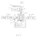
- FIG. 3is a schematic diagram of a reactor system for producing multi-layer packaging according to the present invention.
- FIG. 1illustrates an example of components and a substrate of an implantable medical device 20 with three-dimensional conformal packaging according to the present invention.
- Device 20includes a plurality of three-dimensional components, such as transistor 8 , micro-electro-mechanical system 9 and conductive bonding 10 , on a substrate 23 which can be flexible or rigid as desired.
- a biocompatible multi-layer coating 22 applied by vapour depositionconforms to and sealingly covers at least a portion of the components 8 , 9 , 10 and the substrate 23 .
- the coating 22is applied in at least two sets 24 , 26 , as illustrated schematically in FIG. 2 , to form coating 22 a over component 2 of device 20 a with substrate 23 a .
- Each sethas at least first, second and third layers, such as layers 3 , 4 and 5 of set 24 .
- At least one of the first, second and third layersconsist essentially of a polymer such as parylene and at least one of the other two layers of the set consist essentially of inorganic material such that each layer differs in at least one diffusion barrier property from the other layers in the set, for example differing in diffusion behaviour through each layer relative to the other layers.
- the barrier property for the transport of impuritiesis dominated more by the interface between two adjacent layers than by the thickness of each individual layer.
- the diffusion behaviour of each layeris additive to that of the other layers, and set 26 repeats the same sequence of layers with layers 6 , 7 , 7 ′ (not shown) etc. As many sets of layers can be applied as desired.
- an additional treatmentsuch as a gas plasma, or an additional layer is added to improve the interface between two layers, especially with respect to impurity diffusion.
- Deposition chamber 103can be utilized for a thermal process, such as a conventional Gorham process, or a plasma enhanced process.
- a thermal processsuch as for parylene deposition
- a vaporization chamber 101is provided to vaporize a solid parylene precursor, for example a stable di-cyclic dimer, di-p-xylylene, or halogenated derivatives at temperature between 110° and 200° C.
- the vaporized precursorthen passes to a pyrolysis chamber 102 to decompose the dimer in reactive species, such as monomers, at temperatures between 400° C. and 700° C.
- reactive speciessuch as monomers
- typical parametersare 150° C.
- the pyrolized precursorthen passes from the pyrolysis chamber through a gate valve 108 to the medical devices to be treated on a sample holder 111 in the deposition chamber 103 .
- Typical parylene layer thicknessis between 10 nm-100 microns.
- the precursor vapour pressure in the deposition chamber 103is approximately between 1 and 10 Pa, typically 7 Pa, and the substrate temperature is substantially at room temperature.
- the remaining vapour mixturethen passes from deposition chamber 103 to a cold trap 104 connected to a vacuum pump 105 .
- gate valves 107 and 112are closed.
- the deposition process performed in chamber 103can be either an external downstream plasma enhanced chemical vapour deposition (PECVD) facility or an in-situ plasma enhanced process.
- the downstream reactoris composed of a plasma tube 113 and a coil 114 around the plasma tube connected to the RF generator 115 .
- the tube 113is in gaseous communication with the gas source 116 and the deposition chamber 103 .
- the desired amounts and proportions of gases supplied by gas source 116 introduced into the plasma tube 113may be regulated using one or more mass flow controllers.
- the capacitively and/or inductively coupled high frequency plasmais utilized to excite and/or dissociate most of the entering process gas created by organic or inorganic precursors.
- This reactive gasis then injected in the deposition chamber 103 through a valve 112 that is alternatively opened and closed in counter phase with the gate valve 108 for parylene deposition.
- the valve 107is open to evacuate parylene via a bypass 106 to the cold trap 104 .
- the power of the generatoris between 10 to 500 Watts according to the specific reactor size.
- controlled plasmais formed adjacent to the medical device wafers by RF energy applied to sample holder 111 from RF generator 109 , with the deposition chamber 103 grounded, via a high frequency sealed pass-through connector 110 .
- RF generator 109can supply a high RF frequency of typically 13.56 MHz or 2.45 GHz to the sample holder 111 to enhance the decomposition and/or excitation of reactive species introduced into chamber.
- one of the inorganic layersis SiNx for its low permeability and low film stress characteristics.
- the deposition conditionsare 130 sccm of SiH4 (5% in argon), 20 sccm NH3, 100-180 W RF power, 800 mTorr chamber pressure, and 80-120° C. substrate temperature.
- thicknesses between 10-300 nmare deposited.
- Other gasescould be used, as for example SiH4/NH3/H2 or SiH4/N2.
- one of the inorganic layersis SiOx for its well established process.
- the deposition conditionsare 150 sccm SiH4, 100 sccm N2O, 30-80 W RF power, 800 mTorr pressure, and 80° C. substrate temperature.
- thicknesses between 10-300 nmare deposited.
- gasescould be used, as for example SiH4/N2O/Ar or HMDS/O2.
- metalsinclude, but are not limited to, titanium, aurum, platinum, argentum, ferrum, aluminum, nickel, indium, tantalum, tin, zirconium, chromium, zinc, barium, calcium, sodium, alloys thereof, and combinations thereof.
- Metal oxidesinclude, but are not limited to a compound of oxygen and the metals mentioned above and combinations thereof. Some examples are titanium oxide, aluminum oxide, calcium oxide, sodium oxide, zirconium oxide.
- Metal nitridesinclude, but are not limited to a compound of nitrogen and the metals mentioned above and combinations thereof. Some examples are aluminum nitride titanium nitride.
- Metal carbidesinclude, but are not limited to a compound of carbon and the metals mentioned above and combinations thereof.
- Metal oxynitridesinclude, but are not limited to a compound of oxygen, nitrogen and the metals mentioned above and combinations thereof.
- Other inorganic materialscould be used, but not limited to, are semi-metals, semi-metal oxides, semi-metal nitrides, semi-metalcarbides, semi-metal oxynitrides and combinations thereof.
- materialsare, but not limited to, silicon, germanium, boron, silicon oxide, silicon nitride, silicon oxynitride, germanium oxide, germanium nitride, germanium oxynitride, boron oxide, boron nitride, boron oxynitride and combinations thereof.
- Other inorganic biocompatible materials which can be depositedare calcium phosphate, barium sulfides, and barium oxysulfides.
- amorphous materialsare based on, but not limited to, silicon, boron, carbon, titanium, aluminum, zirconium and hydroxylapatite and combinations thereof.
- Layer on substrate adhesion or layer on layer adhesioncould be improved by different processes.
- silanization or gas plasma treatmentare used for example oxygen, nitrogen or air plasma is applied directly in the deposition chamber 103 before coating.
- other adhesion layer or plasma enhanced deposition layercan be used.
- a well known adhesion layer based on silanesare composed of vinyl trichlorosilane in either xylene, isopropyl alcohol or a chlorofluorocarbon gas.
- gammamethacryloxypropyltrimethoxysilane in a methanol-water solventhave been successfully used.
- Silanescan also be vapour phase applied if non-liquid application is preferred.
Landscapes
- Engineering & Computer Science (AREA)
- Manufacturing & Machinery (AREA)
- Microelectronics & Electronic Packaging (AREA)
- Laminated Bodies (AREA)
- Materials For Medical Uses (AREA)
- Prostheses (AREA)
- Chemical Vapour Deposition (AREA)
Abstract
Description
Claims (13)
Priority Applications (6)
| Application Number | Priority Date | Filing Date | Title |
|---|---|---|---|
| US12/854,298US8313819B2 (en) | 2009-08-12 | 2010-08-11 | Ultra-thin multi-layer packaging |
| CA2770611ACA2770611C (en) | 2009-08-12 | 2010-08-12 | Ultra-thin multi-layer packaging |
| PCT/IB2010/002197WO2011018709A2 (en) | 2009-08-12 | 2010-08-12 | Ultra-thin multi-layer packaging |
| AU2010283553AAU2010283553B2 (en) | 2009-08-12 | 2010-08-12 | Ultra-thin multi-layer packaging |
| EP10760419.1AEP2464421B1 (en) | 2009-08-12 | 2010-08-12 | Ultra-thin multi-layer packaging |
| PL10760419TPL2464421T3 (en) | 2009-08-12 | 2010-08-12 | Ultra-thin multi-layer packaging |
Applications Claiming Priority (2)
| Application Number | Priority Date | Filing Date | Title |
|---|---|---|---|
| US23339509P | 2009-08-12 | 2009-08-12 | |
| US12/854,298US8313819B2 (en) | 2009-08-12 | 2010-08-11 | Ultra-thin multi-layer packaging |
Publications (2)
| Publication Number | Publication Date |
|---|---|
| US20110039050A1 US20110039050A1 (en) | 2011-02-17 |
| US8313819B2true US8313819B2 (en) | 2012-11-20 |
Family
ID=43128352
Family Applications (1)
| Application Number | Title | Priority Date | Filing Date |
|---|---|---|---|
| US12/854,298Active2031-01-05US8313819B2 (en) | 2009-08-12 | 2010-08-11 | Ultra-thin multi-layer packaging |
Country Status (6)
| Country | Link |
|---|---|
| US (1) | US8313819B2 (en) |
| EP (1) | EP2464421B1 (en) |
| AU (1) | AU2010283553B2 (en) |
| CA (1) | CA2770611C (en) |
| PL (1) | PL2464421T3 (en) |
| WO (1) | WO2011018709A2 (en) |
Cited By (5)
| Publication number | Priority date | Publication date | Assignee | Title |
|---|---|---|---|---|
| US20210137379A1 (en)* | 2018-10-17 | 2021-05-13 | Jean-Noel Fehr | Intraocular lenses with embedded intraocular pressure sensors |
| US11122975B2 (en) | 2017-05-12 | 2021-09-21 | California Institute Of Technology | Implantable extracompartmental pressure sensor |
| US11291377B2 (en) | 2015-03-31 | 2022-04-05 | California Institute Of Technology | Biocompatible packaging for long term implantable sensors and electronics |
| US11497399B2 (en) | 2016-05-31 | 2022-11-15 | Qura, Inc. | Implantable intraocular pressure sensors and methods of use |
| US11701504B2 (en) | 2020-01-17 | 2023-07-18 | California Institute Of Technology | Implantable intracranial pressure sensor |
Families Citing this family (15)
| Publication number | Priority date | Publication date | Assignee | Title |
|---|---|---|---|---|
| US8361591B2 (en)* | 2009-08-12 | 2013-01-29 | Medos International Sarl | Packaging with active protection layer |
| US8313811B2 (en)* | 2009-08-12 | 2012-11-20 | Medos International S.A.R.L. | Plasma enhanced polymer ultra-thin multi-layer packaging |
| US8313819B2 (en) | 2009-08-12 | 2012-11-20 | Medos International S.A.R.L. | Ultra-thin multi-layer packaging |
| US8590387B2 (en) | 2011-03-31 | 2013-11-26 | DePuy Synthes Products, LLC | Absolute capacitive micro pressure sensor |
| US9156055B2 (en)* | 2012-01-10 | 2015-10-13 | Hzo, Inc. | Precursor supplies, material processing systems with which precursor supplies are configured to be used and associated methods |
| US9345813B2 (en)* | 2012-06-07 | 2016-05-24 | Medos International S.A.R.L. | Three dimensional packaging for medical implants |
| DE102016106137B4 (en)* | 2016-04-04 | 2023-12-28 | Infineon Technologies Ag | Electronic device housing comprising a dielectric layer and an encapsulating material |
| JP2019533179A (en)* | 2016-07-21 | 2019-11-14 | ジョンソン・アンド・ジョンソン・ビジョン・ケア・インコーポレイテッドJohnson & Johnson Vision Care, Inc. | Biomedical device including inclusion body |
| EP3319098A1 (en) | 2016-11-02 | 2018-05-09 | Abiomed Europe GmbH | Intravascular blood pump comprising corrosion resistant permanent magnet |
| FR3061404B1 (en)* | 2016-12-27 | 2022-09-23 | Packaging Sip | METHOD FOR THE COLLECTIVE MANUFACTURING OF HERMETIC ELECTRONIC MODULES |
| US11617891B2 (en)* | 2017-07-21 | 2023-04-04 | Shenzhen Cas-Envision Medical Technology Co., Ltd | Implantable medical device having package and method for packaging implantable medical device |
| DK3567619T3 (en)* | 2018-05-08 | 2021-01-04 | Abiomed Europe Gmbh | CORROSION RESISTANT PERMANENT MAGNET AND INTRAVASCULAR BLOOD PUMP INCLUDING MAGNET |
| WO2020023036A1 (en)* | 2018-07-25 | 2020-01-30 | Qura, Inc. | Implantable intraocular pressure sensors configured as capsular tension rings |
| NL2021497B1 (en) | 2018-08-24 | 2020-02-27 | Salvia Bioelectronics Bv | An electrical stimulation device for body tissue |
| WO2020114617A1 (en)* | 2018-12-07 | 2020-06-11 | Pixium Vision Sa | Hermetic packaging of electronic components |
Citations (60)
| Publication number | Priority date | Publication date | Assignee | Title |
|---|---|---|---|---|
| US4206762A (en) | 1976-06-21 | 1980-06-10 | Cosman Eric R | Telemetric differential pressure sensing method |
| US4237900A (en) | 1979-02-14 | 1980-12-09 | Pacesetter Systems, Inc. | Implantable calibration means and calibration method for an implantable body transducer |
| US4281667A (en) | 1976-06-21 | 1981-08-04 | Cosman Eric R | Single diaphragm telemetric differential pressure sensing system |
| US4676255A (en) | 1985-07-03 | 1987-06-30 | Cosman Eric R | Telemetric in-vivo calibration method and apparatus using a negative pressure applicator |
| US4954925A (en) | 1988-12-30 | 1990-09-04 | United Technologies Corporation | Capacitive sensor with minimized dielectric drift |
| US5142912A (en) | 1990-06-15 | 1992-09-01 | Honeywell Inc. | Semiconductor pressure sensor |
| US5361218A (en) | 1992-08-11 | 1994-11-01 | Itt Corporation | Self-calibrating sensor |
| US5444901A (en) | 1993-10-25 | 1995-08-29 | United Technologies Corporation | Method of manufacturing silicon pressure sensor having dual elements simultaneously mounted |
| US5609629A (en) | 1995-06-07 | 1997-03-11 | Med Institute, Inc. | Coated implantable medical device |
| US5629008A (en) | 1992-06-02 | 1997-05-13 | C.R. Bard, Inc. | Method and device for long-term delivery of drugs |
| EP0992609A1 (en) | 1998-09-30 | 2000-04-12 | Becton, Dickinson and Company | Process for depositing a barrier coating on plastic objects |
| US6144106A (en) | 1996-10-04 | 2000-11-07 | Dow Corning Corporation | Electronic coatings |
| US20020038134A1 (en) | 1999-03-24 | 2002-03-28 | Greenberg Robert J. | Package for an implantable medical device |
| US20020045921A1 (en) | 2000-10-16 | 2002-04-18 | Remon Medical Technologies Ltd. | Implantable pressure sensors and methods for making and using them |
| US20020172811A1 (en) | 2001-05-16 | 2002-11-21 | International Business Machines Corporation | Laminated diffusion barrier |
| US20020185712A1 (en) | 2001-06-08 | 2002-12-12 | Brian Stark | Circuit encapsulation technique utilizing electroplating |
| US6570325B2 (en) | 1998-12-16 | 2003-05-27 | Battelle Memorial Institute | Environmental barrier material for organic light emitting device and method of making |
| US6635014B2 (en) | 2000-01-21 | 2003-10-21 | Timothy J. Starkweather | Ambulatory medical apparatus and method having telemetry modifiable control software |
| US6703462B2 (en) | 2001-08-09 | 2004-03-09 | Dielectric Systems Inc. | Stabilized polymer film and its manufacture |
| US6709715B1 (en) | 1999-06-17 | 2004-03-23 | Applied Materials Inc. | Plasma enhanced chemical vapor deposition of copolymer of parylene N and comonomers with various double bonds |
| US6716444B1 (en) | 2000-09-28 | 2004-04-06 | Advanced Cardiovascular Systems, Inc. | Barriers for polymer-coated implantable medical devices and methods for making the same |
| US6774278B1 (en) | 1995-06-07 | 2004-08-10 | Cook Incorporated | Coated implantable medical device |
| US20040229051A1 (en) | 2003-05-15 | 2004-11-18 | General Electric Company | Multilayer coating package on flexible substrates for electro-optical devices |
| US7007551B2 (en) | 2003-12-11 | 2006-03-07 | Proteus Biomedical, Inc. | Pressure sensors having transducers positioned to provide for low drift |
| US20060083772A1 (en) | 2004-04-06 | 2006-04-20 | Dewitt David M | Coating compositions for bioactive agents |
| US20060111791A1 (en) | 2002-07-29 | 2006-05-25 | Peter Forsell | Durable implant |
| WO2006063157A2 (en) | 2004-12-09 | 2006-06-15 | Boston Scientific Scimed, Inc. | Medical devices having vapor deposited nanoporous coatings for controlled therapeutic agent delivery |
| US20060147492A1 (en) | 2003-11-10 | 2006-07-06 | Angiotech International Ag | Medical implants and anti-scarring agents |
| US20060173497A1 (en) | 2005-02-01 | 2006-08-03 | Brian Mech | Micro-miniature implantable coated device |
| US7131334B2 (en) | 2004-04-19 | 2006-11-07 | Celerity, Inc. | Pressure sensor device and method |
| US20070096281A1 (en) | 2005-11-02 | 2007-05-03 | Greenberg Robert J | Implantable microelectronic device and method of manufacture |
| US20070128420A1 (en) | 2005-12-07 | 2007-06-07 | Mariam Maghribi | Hybrid composite for biological tissue interface devices |
| US20070158100A1 (en) | 2002-08-09 | 2007-07-12 | Robert Greenberg | Insulated implantable electrical circuit |
| US20070216300A1 (en) | 2002-04-04 | 2007-09-20 | International Display Systems, Inc. | Organic opto-electronic device with environmentally protective barrier |
| US7334480B2 (en) | 2004-10-18 | 2008-02-26 | Silverbrook Research Pty Ltd | Dual membrane sensor for temperature compensated pressure sensing |
| US7347826B1 (en) | 2003-10-16 | 2008-03-25 | Pacesetter, Inc. | Packaging sensors for long term implant |
| WO2008039543A1 (en) | 2006-09-27 | 2008-04-03 | University Of Connecticut | Implantable biosensor and methods of use thereof |
| US7364925B2 (en) | 2002-04-04 | 2008-04-29 | International Display Systems, Inc. | Organic light emitting device having a protective barrier |
| US20080185173A1 (en) | 2007-02-07 | 2008-08-07 | Bedinger John M | Environmental Protection Coating System and Method |
| US7413547B1 (en) | 2004-11-08 | 2008-08-19 | Transoma Medical, Inc. | Reference sensor correction for implantable sensors |
| US20080200750A1 (en) | 2006-11-17 | 2008-08-21 | Natalie James | Polymer encapsulation for medical device |
| US20080306554A1 (en) | 2007-06-11 | 2008-12-11 | Mckinley Laurence M | Osseointegration and biointegration coatings for bone screw implants |
| US7464598B2 (en) | 2004-10-18 | 2008-12-16 | Silverbrook Research Pty Ltd | Method of pressure sensing with a pressure sensor having a sensor membrane and a compensation membrane |
| US20090004241A1 (en) | 2007-06-08 | 2009-01-01 | Northwestern University | Polymer nanofilm coatings |
| US20090036754A1 (en) | 2007-07-31 | 2009-02-05 | Captomed Eurl | Self-calibrating pressure sensor |
| US20090110892A1 (en) | 2004-06-30 | 2009-04-30 | General Electric Company | System and method for making a graded barrier coating |
| US20090124965A1 (en) | 2007-07-27 | 2009-05-14 | Greenberg Robert J | Implantable device for the brain |
| US20090142227A1 (en) | 2005-07-01 | 2009-06-04 | Manfred Fuchs | Parylene Coating and Method for the Production Thereof |
| US20090192580A1 (en) | 2008-01-28 | 2009-07-30 | Shrojalkumar Desai | Medical electrical lead with biocompatible lead body coating |
| US7580754B2 (en) | 2003-11-14 | 2009-08-25 | Cochlear Limited | Implantable acoustic sensor |
| US20090254146A1 (en) | 2008-04-03 | 2009-10-08 | Giorgio Bonmassar | Deep brain stimulation implant with microcoil array |
| US20090263641A1 (en) | 2008-04-16 | 2009-10-22 | Northeast Maritime Institute, Inc. | Method and apparatus to coat objects with parylene |
| US20090263581A1 (en) | 2008-04-16 | 2009-10-22 | Northeast Maritime Institute, Inc. | Method and apparatus to coat objects with parylene and boron nitride |
| US7611533B2 (en) | 1995-06-07 | 2009-11-03 | Cook Incorporated | Coated implantable medical device |
| US20090297813A1 (en) | 2004-06-30 | 2009-12-03 | General Electric Company | System and method for making a graded barrier coating |
| US20100005851A1 (en) | 2005-10-27 | 2010-01-14 | Advanced Research Corporation | Self-calibrating pressure sensor |
| US20110015686A1 (en) | 2009-07-16 | 2011-01-20 | Sule Kara | Sealing of an implantable medical device |
| US20110038131A1 (en) | 2009-08-12 | 2011-02-17 | Medos International Sarl | Packaging with active protection layer |
| US20110038130A1 (en) | 2009-08-12 | 2011-02-17 | Medos International Sarl | Plasma enhanced polymer ultra-thin multi-layer packaging |
| US20110039050A1 (en) | 2009-08-12 | 2011-02-17 | Medos International Sarl | Ultra-thin multi-layer protection |
Family Cites Families (1)
| Publication number | Priority date | Publication date | Assignee | Title |
|---|---|---|---|---|
| US5955161A (en)* | 1996-01-30 | 1999-09-21 | Becton Dickinson And Company | Blood collection tube assembly |
- 2010
- 2010-08-11USUS12/854,298patent/US8313819B2/enactiveActive
- 2010-08-12EPEP10760419.1Apatent/EP2464421B1/enactiveActive
- 2010-08-12CACA2770611Apatent/CA2770611C/enactiveActive
- 2010-08-12PLPL10760419Tpatent/PL2464421T3/enunknown
- 2010-08-12WOPCT/IB2010/002197patent/WO2011018709A2/enactiveApplication Filing
- 2010-08-12AUAU2010283553Apatent/AU2010283553B2/ennot_activeCeased
Patent Citations (65)
| Publication number | Priority date | Publication date | Assignee | Title |
|---|---|---|---|---|
| US4281667A (en) | 1976-06-21 | 1981-08-04 | Cosman Eric R | Single diaphragm telemetric differential pressure sensing system |
| US4206762A (en) | 1976-06-21 | 1980-06-10 | Cosman Eric R | Telemetric differential pressure sensing method |
| US4237900A (en) | 1979-02-14 | 1980-12-09 | Pacesetter Systems, Inc. | Implantable calibration means and calibration method for an implantable body transducer |
| US4676255A (en) | 1985-07-03 | 1987-06-30 | Cosman Eric R | Telemetric in-vivo calibration method and apparatus using a negative pressure applicator |
| US4954925A (en) | 1988-12-30 | 1990-09-04 | United Technologies Corporation | Capacitive sensor with minimized dielectric drift |
| US5142912A (en) | 1990-06-15 | 1992-09-01 | Honeywell Inc. | Semiconductor pressure sensor |
| US5629008A (en) | 1992-06-02 | 1997-05-13 | C.R. Bard, Inc. | Method and device for long-term delivery of drugs |
| US5361218A (en) | 1992-08-11 | 1994-11-01 | Itt Corporation | Self-calibrating sensor |
| US5444901A (en) | 1993-10-25 | 1995-08-29 | United Technologies Corporation | Method of manufacturing silicon pressure sensor having dual elements simultaneously mounted |
| US6774278B1 (en) | 1995-06-07 | 2004-08-10 | Cook Incorporated | Coated implantable medical device |
| US7611533B2 (en) | 1995-06-07 | 2009-11-03 | Cook Incorporated | Coated implantable medical device |
| US6096070A (en) | 1995-06-07 | 2000-08-01 | Med Institute Inc. | Coated implantable medical device |
| US5609629A (en) | 1995-06-07 | 1997-03-11 | Med Institute, Inc. | Coated implantable medical device |
| US20080132992A1 (en) | 1995-06-07 | 2008-06-05 | Cook Incorporated | Coated implantable medical device |
| US6144106A (en) | 1996-10-04 | 2000-11-07 | Dow Corning Corporation | Electronic coatings |
| EP0992609A1 (en) | 1998-09-30 | 2000-04-12 | Becton, Dickinson and Company | Process for depositing a barrier coating on plastic objects |
| US6570325B2 (en) | 1998-12-16 | 2003-05-27 | Battelle Memorial Institute | Environmental barrier material for organic light emitting device and method of making |
| US20020038134A1 (en) | 1999-03-24 | 2002-03-28 | Greenberg Robert J. | Package for an implantable medical device |
| US6709715B1 (en) | 1999-06-17 | 2004-03-23 | Applied Materials Inc. | Plasma enhanced chemical vapor deposition of copolymer of parylene N and comonomers with various double bonds |
| US6635014B2 (en) | 2000-01-21 | 2003-10-21 | Timothy J. Starkweather | Ambulatory medical apparatus and method having telemetry modifiable control software |
| US6716444B1 (en) | 2000-09-28 | 2004-04-06 | Advanced Cardiovascular Systems, Inc. | Barriers for polymer-coated implantable medical devices and methods for making the same |
| US20020045921A1 (en) | 2000-10-16 | 2002-04-18 | Remon Medical Technologies Ltd. | Implantable pressure sensors and methods for making and using them |
| US20020172811A1 (en) | 2001-05-16 | 2002-11-21 | International Business Machines Corporation | Laminated diffusion barrier |
| US20020185712A1 (en) | 2001-06-08 | 2002-12-12 | Brian Stark | Circuit encapsulation technique utilizing electroplating |
| US6703462B2 (en) | 2001-08-09 | 2004-03-09 | Dielectric Systems Inc. | Stabilized polymer film and its manufacture |
| US7364925B2 (en) | 2002-04-04 | 2008-04-29 | International Display Systems, Inc. | Organic light emitting device having a protective barrier |
| US20070216300A1 (en) | 2002-04-04 | 2007-09-20 | International Display Systems, Inc. | Organic opto-electronic device with environmentally protective barrier |
| US20060111791A1 (en) | 2002-07-29 | 2006-05-25 | Peter Forsell | Durable implant |
| US20070158100A1 (en) | 2002-08-09 | 2007-07-12 | Robert Greenberg | Insulated implantable electrical circuit |
| US20040229051A1 (en) | 2003-05-15 | 2004-11-18 | General Electric Company | Multilayer coating package on flexible substrates for electro-optical devices |
| US7347826B1 (en) | 2003-10-16 | 2008-03-25 | Pacesetter, Inc. | Packaging sensors for long term implant |
| US20060147492A1 (en) | 2003-11-10 | 2006-07-06 | Angiotech International Ag | Medical implants and anti-scarring agents |
| US7580754B2 (en) | 2003-11-14 | 2009-08-25 | Cochlear Limited | Implantable acoustic sensor |
| US7007551B2 (en) | 2003-12-11 | 2006-03-07 | Proteus Biomedical, Inc. | Pressure sensors having transducers positioned to provide for low drift |
| US20060083772A1 (en) | 2004-04-06 | 2006-04-20 | Dewitt David M | Coating compositions for bioactive agents |
| US7131334B2 (en) | 2004-04-19 | 2006-11-07 | Celerity, Inc. | Pressure sensor device and method |
| US20090297813A1 (en) | 2004-06-30 | 2009-12-03 | General Electric Company | System and method for making a graded barrier coating |
| US20090110892A1 (en) | 2004-06-30 | 2009-04-30 | General Electric Company | System and method for making a graded barrier coating |
| US7334480B2 (en) | 2004-10-18 | 2008-02-26 | Silverbrook Research Pty Ltd | Dual membrane sensor for temperature compensated pressure sensing |
| US7464598B2 (en) | 2004-10-18 | 2008-12-16 | Silverbrook Research Pty Ltd | Method of pressure sensing with a pressure sensor having a sensor membrane and a compensation membrane |
| US7413547B1 (en) | 2004-11-08 | 2008-08-19 | Transoma Medical, Inc. | Reference sensor correction for implantable sensors |
| WO2006063157A2 (en) | 2004-12-09 | 2006-06-15 | Boston Scientific Scimed, Inc. | Medical devices having vapor deposited nanoporous coatings for controlled therapeutic agent delivery |
| US20060173497A1 (en) | 2005-02-01 | 2006-08-03 | Brian Mech | Micro-miniature implantable coated device |
| US20080051862A1 (en) | 2005-02-01 | 2008-02-28 | Brian Mech | Micro-Miniature Implantable Coated Device |
| US20090142227A1 (en) | 2005-07-01 | 2009-06-04 | Manfred Fuchs | Parylene Coating and Method for the Production Thereof |
| US20100005851A1 (en) | 2005-10-27 | 2010-01-14 | Advanced Research Corporation | Self-calibrating pressure sensor |
| US20070096281A1 (en) | 2005-11-02 | 2007-05-03 | Greenberg Robert J | Implantable microelectronic device and method of manufacture |
| US20070128420A1 (en) | 2005-12-07 | 2007-06-07 | Mariam Maghribi | Hybrid composite for biological tissue interface devices |
| WO2008039543A1 (en) | 2006-09-27 | 2008-04-03 | University Of Connecticut | Implantable biosensor and methods of use thereof |
| US20080200750A1 (en) | 2006-11-17 | 2008-08-21 | Natalie James | Polymer encapsulation for medical device |
| US20090291200A1 (en) | 2007-02-07 | 2009-11-26 | Raytheon Company | Environmental Protection Coating System and Method |
| US20090288876A1 (en) | 2007-02-07 | 2009-11-26 | Raytheon Company | Environmental Protection Coating System and Method |
| US20080185173A1 (en) | 2007-02-07 | 2008-08-07 | Bedinger John M | Environmental Protection Coating System and Method |
| US20090004241A1 (en) | 2007-06-08 | 2009-01-01 | Northwestern University | Polymer nanofilm coatings |
| US20080306554A1 (en) | 2007-06-11 | 2008-12-11 | Mckinley Laurence M | Osseointegration and biointegration coatings for bone screw implants |
| US20090124965A1 (en) | 2007-07-27 | 2009-05-14 | Greenberg Robert J | Implantable device for the brain |
| US20090036754A1 (en) | 2007-07-31 | 2009-02-05 | Captomed Eurl | Self-calibrating pressure sensor |
| US20090192580A1 (en) | 2008-01-28 | 2009-07-30 | Shrojalkumar Desai | Medical electrical lead with biocompatible lead body coating |
| US20090254146A1 (en) | 2008-04-03 | 2009-10-08 | Giorgio Bonmassar | Deep brain stimulation implant with microcoil array |
| US20090263581A1 (en) | 2008-04-16 | 2009-10-22 | Northeast Maritime Institute, Inc. | Method and apparatus to coat objects with parylene and boron nitride |
| US20090263641A1 (en) | 2008-04-16 | 2009-10-22 | Northeast Maritime Institute, Inc. | Method and apparatus to coat objects with parylene |
| US20110015686A1 (en) | 2009-07-16 | 2011-01-20 | Sule Kara | Sealing of an implantable medical device |
| US20110038131A1 (en) | 2009-08-12 | 2011-02-17 | Medos International Sarl | Packaging with active protection layer |
| US20110038130A1 (en) | 2009-08-12 | 2011-02-17 | Medos International Sarl | Plasma enhanced polymer ultra-thin multi-layer packaging |
| US20110039050A1 (en) | 2009-08-12 | 2011-02-17 | Medos International Sarl | Ultra-thin multi-layer protection |
Non-Patent Citations (65)
| Title |
|---|
| Affinito, J.D. et al; A New Method for Fabricating Transparent Barrier Layers; Thin Solid Films (1996); pp. 63-67; 290-291; 1996 Published by Elsevier Science S.A. |
| Affinito, John., et al; Vacuum deposited polymer / metal multilayer films for optical application; Thin Solid Films; (1995); pp. 43-48; vol. 270; © 1995 Elsevier Science S.A., US. |
| Balestreri, M. et al; Impact of Intracranial Pressure and Cerebral Perfusion Pressure on Severe Disability and Mortality After Head Injury; Neurocritical Care; 2006; pp. 8-13; vol. 04: Humana Pess Inc.; ISSN 1541-6933/06/4:8-13. |
| Blenkiewicz, J.; Plasma-Enhanced Parylene Coating for Medical Device Applications; Medical Device Technology; Jan./Feb. 2006; pp. 10-11; vol. 17. No. 1; www.medicaldevicesonline.com; US. |
| Bork, T. et al; Development and in-vitro characterization of an implantable flow sensing transducer for hydrocephalus; Biomedical Microdevices, vol. 12, No. 4, 607-618, DOI: 10.1007/s10544-010-9413-6; SpringerLink Date: Mar. 13, 2010. |
| Boyd, B.; Advanced coating technologies for lead-free solders; Global SMT & Packaging. Jun. 2007, pp. 10-12; www.globalsmt.net. |
| Callahan, R. et al.; Etching parylene-N using a remote oxygen microwave plasma; J. Vac. Sci. Technol. B, Sep./Oct. 2002; pps. vol. 20, No. 5; pp. 1870-1877; © 2002 American Vacuum Society. |
| Callahan, Russell R.A. et al; Downstream oxygen etching characteristics of polymers from the parylene family; J. Vac. Sci. Technol. B, pp. 1496-1500; vol. 21, No. 4, Jul./Aug. 2003; © 2003 American Vacuum Society. |
| Chang, T.Y. et al; Cell and Protein Compatibility of Parylene-C Surfaces; Langmuir, 2007; pp. 11718-11725; vol. 23, No. 23; 2007 American Chemical Society Published on Web Oct. 4, 2007. |
| Charlson, E.M. et al; Temperature Selective Deposition of Parylene-C; IEEE Transactions on Biomedical Engineering; Feb. 1992; pp. 202-206; vol. 39, No. 2; IEEE, Piscataway, NJ US. |
| Chiang, C.C. et al; Deposition and permeation properties of SiNX/parylene multilayers on polymeric substrates; Surface & Coatings Technology 200 (2006) pp. 5843-5848; www.sciencedirect.com. |
| Chou, Chia-Man, et al; Preparation of Plasma-Polymerized Para-Xylene As an Alternative to Parylene Coating for Biomedical Surface Modification; Surface & Coatings Technology (2010); pp. 1631-1636; vol. 204; Elsevier Science B.V; www.elsevier.com/locate/surfcoat, US. |
| CODMAN® ICP Monitoring System Quick set-up Guide; Product Brochure © 2001 Codman & Shurtleff, Inc. |
| Czosnyka, M., et al; Monitoring and interpretation of intracranial pressure; J. Neurol. Neurosurg. Psychiatry 2004;75; pp. 813-821; Downloaded from jnnp.bmj.com on Sep. 2, 2009; DOI:10.1136/jnnp.2003.033126. |
| Czosnyka, M., et al; Monitoring of Cerebrovascular Autoregulation: Facts, Myths, and Missing Links; Neurocrit Care (2009) 10 pp. 373-386; Humana Press DOI 10.1007/s12028-008-9175-7. |
| Dribinskiy, Stanislav F. et al; Properties of Various Polyparylenes Deposited by Chemical Vapor Deposition; Paper PS3-TuP12; AVS 53rd International Symposium; Nov. 14, 2006; pp. 1-4; University of Applied Sciences, D-80335 Munich and Plasma-Parylene Coating Services, D-83022 Rosenheim; DE. |
| Feili, D. et al.; Flexible organic field effect transistors for biomedical microimplants using polyimide and parylene C as substrate and insulator layers; J. Micromech. Microeng. (2006); pp. 1555-1561; 16; Institute of Physics Publishing. |
| Hambrecht, F.T.; Biomaterials research in neural prostheses; Biomaterials Jul. 1982; pp. 187-188, vol. 3; Butterworth & Co (Publishers) Ltd. |
| Heetderks, Wiluam J.; RF Powering of Millimeter- and Submillimeter-Sized Neural Prosthetic Implants; IEEE Transactions on Biomedical Engineering; May 1988; pp. 323-327; vol. 35, No. 5; IEEE, Piscataway, NJ US. |
| Hemedex® Cerebral Blood Flow Monitoring System; Product Brochure ©2007 Codman & Shurtleff, Inc. |
| Hsu, Jui-Mei et al.; Characterization of Parylene-C film as an encapsulation material for neural interface devices; 4M Network of Excellence, 4M Knowledge base-papers; Submitted on Nov. 12, 2007-16:23. http://www.4m-net.org/files/papers/4M2007/374451/PID374451.pdf. |
| Huang, Sheng-Jean, et al.; Clinical outcome of severe head injury using three different ICP and CPP protocol-driven therapies; Journal of Clinical Neuroscience (2006)pp. 818-822; 13; Elsevier Ltd. |
| ICP Express(TM); Product Brochure © 2001 Codman & Shurtleff, Inc. |
| ICP Express™; Product Brochure © 2001 Codman & Shurtleff, Inc. |
| Khabari, A. et al: Partially Ionized Beam Deposition of Parylene; Journal of Non-Crystalline Solids (2005); pp. 3536-3541; vol. 351; 2005 Elsevier B.V. |
| Khabari, A., Partially ionized beam deposition of parylene; Journal of Non-Crystalline Solids (2005); pp. 3536-3541; 351; Elsevier B.V. |
| Kokko, K., et al; Composite coating structure in an implantable electronic device; Soldering & Surface Mount Technology; vol. 21 No. 3 (2009); pp. 24-29 © Emerald Group Publishing Limited [ISSN 0954-0911]. |
| Kumar, R.; New Developments in Parylene Technology for Medical Electronics Advancement; Proceedings of the SMTA Medical Electronics Symposium; May 15-17, 2006; pp. 9; Bloomington. Minnesota. USA. |
| Kumar, R: Advances in Adhesion Solutions for Medical Applications; Proceedings of the SMTA Medical Electronics Symposium, Jan. 29-31, 2008, Anaheim, California, USA; rkumar@scscoatings.com. |
| Lahann, J.; Vapor-based polymer coatings for potential biomedical applications; Polymer International (2006); pp. 1361-1370; 55; 2006 Society of Chemical Industry. |
| Lee, L. James; Polymer Nanoengineering for Biomedical Applications; Annals of Biomedical Engineering, Jan. 2006; pp. 75-88; vol. 34, No. 1. |
| Li, P.-Y, et al; A Parylene Bellows Electrochemical Actuator for Intraocular Drug Delivery; Transducers Jun. 21-25, 2009; pp. 1461-1464; 978-1-4244-4193-8/09; IEEE 2009, Piscataway, NJ, USA. |
| Mark, Herman F.; Xylylene Polymers; Concise Encyclopedia of Polymer Science and Technology; 2007; pp. 1384-1389, John Wiley & Sons, USA 2007. |
| Meng, E. et al; Plasma Removal of Parylene C; J. Micromech. Microeng. (2008), pp. 1-13; 18 045004; IOP Publishing; http://iopscience.iop.org, US. |
| Mitu, B., et al; Plasma-deposited parylene-like thin films: process and material properties; Surface and Coatings Technology (2003), pp. 174-175; Issue 124-130; Elsevier Science B.V; www.sciencedirect.com. |
| Mitu, B., et al; Plasma-Deposited Parylene-Like Thin Films: Process and Material Properties; Surface and Coatings Technology; (2003) pp. 124-130; 174-175; Elsevier Science B.V; www.sciencedirect.com, US. |
| Momentive Performance Materials: Silquest A-174* Silane Product Brochure; Copyright 2003-2007 Momentive Performance Materials Inc., Wilton, CT, USA. |
| Nicholas, M.F. et al; Functional Hermetic Encapsulation of Integrated Circuits; ISA, 1991-pp. 331-339; Paper 091-043 0067-8856/91; ISA Publishing; Research Triangle Park, NC, USA; The British Library, UK. |
| North, B.; Intracranial Pressure Monitoring; Head Injury; 1997; pp. 209-216; 10; Chapman & Hall, London. |
| Pang, C.; Parylene Technology for Neural Probes Applications; Thesis for the Degree of Doctor of Philosophy; Sep. 17, 2007; pp. vii-viii and pp. 1-139; California Institute of Technology, Pasadena, CA, USA 2008. |
| Pruden, K.G. et al; Ammonium chloride complex formation during downstream microwave ammonia plasma treatment of parylene-C; J. Vac. Sci. Technol. A, Nov./Dec. 2005; pp. 1605-1609; vol. 23, No. 6. |
| Pruden, K.G. et al; Characterization of Parylene-N and Parylene-C Photooxidation; Journal of Polymer Science: Part A: Polymer Chemistry, pp. 1486-1496; vol. 41, (2003) © 2003 Wiley Periodicals, Inc. |
| Ratanalert, Sanguansin, M.D. et al; ICP Threshold in CPP Management of Severe Head Injury Patients; Surg. Neurol.; 2004; pp. 429-434; 61; © 2004 Elsevier Inc. 360 Park Avenue South, New York, NY 10010-17. |
| Ratier, Bernard; Vapor Deposition Polymerization and Reactive Ion Beam Etching of poly(p-xylylene) Films for Waveguide Applications; Optical Materials; (1999); pp. 229-233; vol. 12; 1999 Elsevier Science B.V. |
| Rodger, D.C.; et al.; Flexible parylene-based multielectrode array technology for high-density neural stimulation and recording; Sensors and Actuators B (2008); pp. 449-460; 132; Elsevier B.V. |
| Ruckh, R. et al; Model Calculation of Polymer Heterostructures; Physica Scripta. 1988; pp. 122-124; vol. 38, Institute of Physics Publishing (IOP) on behalf of the Royal Swedish Academy of Sciences; Academies of Sciences and Physical Societies; Sweden. |
| Sadhir, R.K.et al.; The adhesion of glow-discharge polymers, Silastic and Parylene to implantable platinum electrodes: results of tensile pull tests after exposure to isotonic sodium chloride; Biomaterials 1981, pp. 239-243, vol. 2, October. |
| Senkevich, J.J. et al.; The facile surface modification of poly(p-xylylene) ultrathin Films; Colloids and Surfaces A: Physicochem. Eng. Aspects; (2003); pp. 167-173; 216; Elsevier Science B.V. |
| Seong, J.W. et al; Effects of ion bombardment with reactive gas environment on adhesion of Au films to Parylene C film; Thin Solid Films 476 (2005) pp. 386-390; © 2004 Elsevier B.V.; www.sciencedirect.com. |
| Seymour, John P, et al; The insulation performance of reactive parylene films in implantable electronic devices; Biomaterials (2009); pp. 6158-6167; 30; Elsevier Ltd. |
| Seymour, John P., et al; Neural Probe Design for Reduced Tissue Encapsulation in CNS; Biomaterials; (2007); pp. 3594-3607; vol. 28, Issue 25; doi:10.1016/j.biomaterials.2007.03.024; Copyright © 2007 Elsevier Ltd, US. |
| Sworecki, K. et al; Modification of Polymer Membranes by Ion Implantation; Nuclear Instruments and Methods in Physics Research; (2004); B 225; pp. 483-488; 2004 Elsevier B.V. |
| Tewari, P. et al; Control of interfaces on electrical properties of SiO2-Parylene-C laminar composite dielectrics; Journal of Colloid and Interface Science 332 (2009) pp. 65-73. |
| V&P Scientific, Inc; Solvent Resistance of Parylenes C,N,D; Technology Letter #10; Revised 05-85; Copyright © 2009, V&P Scientific, Inc. San Diego, CA; http://www.vp-scientific.com/solvent.htm. |
| Von Elm, Erik, et al; Severe traumatic brain injury in Switzerland-feasibility and first results of a cohort study; Swiss Med Wkly 2008;138 (23-24): pp. 327-334 www.smw.ch. |
| Wolgemuth, L.; A Look at Parylene Coatings in Drug-Eluting Technologies; Reprinted from Medical Device & Diagnostic Industry, Aug. 2005; Copyright © 2005 Canon Communications LLC. |
| Wolgemuth, L.; Parylenes: Advanced Polymers for Medical Devices; Specialty Coating Systems, 2006; pp. 1-4; 7645 Woodland Drive, Indianapolis, IN 46278 USA; lwolgemuth@scscoatings.com. |
| Wolgemuth, Lonny; A Look at Parylene Coatings in Drug-Eluting Technologies; Medical Device & Diagnostic Industry; Aug. 1, 2005; Copyright © 2005 Medical Device & Diagnostic Industry. |
| Wolgemuth, Lonny; The Truly Conformal Coating; Medical Device Developments; Apr. 4, 2008; 2 pages; vol. 1; http://www.medicaldevice-network.com/features/feature1818/; Copyright 2011 Net Resources International US. |
| Wright, Dylan, et al; Reusable, Reversibly Sealable Parylene Membranes for Cell and Protein Patterning; Journal of Biomedical Materials Research Part A; May 2008; pp. 530-538; vol. 85A; Article first published online: Aug. 29, 2007; Copyright © 2007 Wiley Periodicals, Inc., A Wiley Company; http://onlinelibrary.wiley.com/doi/10.1002/jbm.a.31281/abstract. |
| Xingding, Zhang; The relationship between GCS, ICP, CPP and glutamate in the cerebrospinal fluid following acute cerebral injury and brain edema in humans; Head Injury-Pathophysiology of Head Injury; Jul. 7, 1997; p. S71; p. 2-159. |
| Yamagishi, F. G.; Investigation of Plasma-Polymerized Films As Primers for Parylene-C Coatngs on Neural Prosthesis Materials; Metallurgical and Protective Layers Thin Solid Films, (1991) pp. 39 50; 202; Elsevier Sequoia/Printed in The Netherlands. |
| Yu, Qingsong et al.; Engineering the surface and interface of Parylene C coatings by low-temperature plasmas; Progress in Organic Coatings; (2001); pp. 247-253; 41; 2001 Elsevier Science B.V. |
| Zakar, E. et al; Patterning of Thick Parylene Films by Oxygen Plasma for Application as Exploding Foil Initiator Flyer Material; Army Research Laboratory; Sep. 2009; pp. 1-13; ARL-TR-4956; Adelphia, MD 20783-1197. |
| Zhang, X., et al; Crystallinity properties of parylene-n affecting its use as an ILD in submicron integrated circuit technology; Thin Solid Films 270 (1995) pp. 508-511; Elsevier Science S.A. |
Cited By (6)
| Publication number | Priority date | Publication date | Assignee | Title |
|---|---|---|---|---|
| US11291377B2 (en) | 2015-03-31 | 2022-04-05 | California Institute Of Technology | Biocompatible packaging for long term implantable sensors and electronics |
| US11497399B2 (en) | 2016-05-31 | 2022-11-15 | Qura, Inc. | Implantable intraocular pressure sensors and methods of use |
| US11122975B2 (en) | 2017-05-12 | 2021-09-21 | California Institute Of Technology | Implantable extracompartmental pressure sensor |
| US20210137379A1 (en)* | 2018-10-17 | 2021-05-13 | Jean-Noel Fehr | Intraocular lenses with embedded intraocular pressure sensors |
| US12178512B2 (en)* | 2018-10-17 | 2024-12-31 | Qura, Inc. | Implantable devices with embedded pressure sensors |
| US11701504B2 (en) | 2020-01-17 | 2023-07-18 | California Institute Of Technology | Implantable intracranial pressure sensor |
Also Published As
| Publication number | Publication date |
|---|---|
| WO2011018709A3 (en) | 2011-04-14 |
| EP2464421B1 (en) | 2016-10-05 |
| AU2010283553B2 (en) | 2015-05-07 |
| WO2011018709A2 (en) | 2011-02-17 |
| PL2464421T3 (en) | 2017-04-28 |
| EP2464421A2 (en) | 2012-06-20 |
| CA2770611C (en) | 2019-02-12 |
| AU2010283553A1 (en) | 2012-04-05 |
| CA2770611A1 (en) | 2011-02-17 |
| US20110039050A1 (en) | 2011-02-17 |
| WO2011018709A8 (en) | 2012-04-12 |
Similar Documents
| Publication | Publication Date | Title |
|---|---|---|
| US8313819B2 (en) | Ultra-thin multi-layer packaging | |
| AU2016201160A1 (en) | Ultra-thin multilayer packaging | |
| US8313811B2 (en) | Plasma enhanced polymer ultra-thin multi-layer packaging | |
| US8361591B2 (en) | Packaging with active protection layer | |
| US9345813B2 (en) | Three dimensional packaging for medical implants | |
| JP5473946B2 (en) | Method for manufacturing multilayer stack structure with improved WVTR barrier property | |
| TWI722987B (en) | Process for producing flexible organic-inorganic laminates | |
| KR20090087457A (en) | Hybrid Layers for Use on Coatings on Electronic Devices or Other Articles | |
| US12347652B2 (en) | Method for forming plasma coating | |
| KR102334075B1 (en) | Dual atmospheric pressure low-temperature plasma device and method for manufacturing an OLED element-modified encapsulation film using the same | |
| JP4556610B2 (en) | Surface-coated plastic material | |
| Raj et al. | Nanostructures for Enabling Implantable Bioelectronic Systems | |
| WO2025051532A1 (en) | Coupling agent, coating system comprising the same, related method and uses |
Legal Events
| Date | Code | Title | Description |
|---|---|---|---|
| AS | Assignment | Owner name:MEDOS INTERNATIONAL S.A.R.L., SWITZERLAND Free format text:ASSIGNMENT OF ASSIGNORS INTEREST;ASSIGNORS:HOGG, ANDREAS;KEPPNER, HERBERT;AELLEN, THEIRRY;AND OTHERS;REEL/FRAME:024942/0480 Effective date:20100903 | |
| STCF | Information on status: patent grant | Free format text:PATENTED CASE | |
| FPAY | Fee payment | Year of fee payment:4 | |
| AS | Assignment | Owner name:INTEGRA LIFESCIENCES SWITZERLAND SARL, SWITZERLAND Free format text:ASSIGNMENT OF ASSIGNORS INTEREST;ASSIGNOR:MEDOS INTERNATIONAL SARL;REEL/FRAME:044741/0552 Effective date:20171002 | |
| AS | Assignment | Owner name:COAT-X SA, SWITZERLAND Free format text:ASSIGNMENT OF ASSIGNORS INTEREST;ASSIGNOR:INTEGRA LIFESCIENCES SWITZERLAND SARL;REEL/FRAME:049481/0776 Effective date:20181214 | |
| FEPP | Fee payment procedure | Free format text:ENTITY STATUS SET TO SMALL (ORIGINAL EVENT CODE: SMAL); ENTITY STATUS OF PATENT OWNER: SMALL ENTITY | |
| MAFP | Maintenance fee payment | Free format text:PAYMENT OF MAINTENANCE FEE, 8TH YR, SMALL ENTITY (ORIGINAL EVENT CODE: M2552); ENTITY STATUS OF PATENT OWNER: SMALL ENTITY Year of fee payment:8 | |
| MAFP | Maintenance fee payment | Free format text:PAYMENT OF MAINTENANCE FEE, 12TH YR, SMALL ENTITY (ORIGINAL EVENT CODE: M2553); ENTITY STATUS OF PATENT OWNER: SMALL ENTITY Year of fee payment:12 |