US8313277B2 - Semiconductor manufacturing process modules - Google Patents
Semiconductor manufacturing process modulesDownload PDFInfo
- Publication number
- US8313277B2 US8313277B2US11/876,915US87691507AUS8313277B2US 8313277 B2US8313277 B2US 8313277B2US 87691507 AUS87691507 AUS 87691507AUS 8313277 B2US8313277 B2US 8313277B2
- Authority
- US
- United States
- Prior art keywords
- vacuum
- handling
- workpiece
- module
- robotic
- Prior art date
- Legal status (The legal status is an assumption and is not a legal conclusion. Google has not performed a legal analysis and makes no representation as to the accuracy of the status listed.)
- Active, expires
Links
Images


Classifications
- H—ELECTRICITY
- H01—ELECTRIC ELEMENTS
- H01L—SEMICONDUCTOR DEVICES NOT COVERED BY CLASS H10
- H01L21/00—Processes or apparatus adapted for the manufacture or treatment of semiconductor or solid state devices or of parts thereof
- H01L21/67—Apparatus specially adapted for handling semiconductor or electric solid state devices during manufacture or treatment thereof; Apparatus specially adapted for handling wafers during manufacture or treatment of semiconductor or electric solid state devices or components ; Apparatus not specifically provided for elsewhere
- H01L21/677—Apparatus specially adapted for handling semiconductor or electric solid state devices during manufacture or treatment thereof; Apparatus specially adapted for handling wafers during manufacture or treatment of semiconductor or electric solid state devices or components ; Apparatus not specifically provided for elsewhere for conveying, e.g. between different workstations
- H01L21/67703—Apparatus specially adapted for handling semiconductor or electric solid state devices during manufacture or treatment thereof; Apparatus specially adapted for handling wafers during manufacture or treatment of semiconductor or electric solid state devices or components ; Apparatus not specifically provided for elsewhere for conveying, e.g. between different workstations between different workstations
- B—PERFORMING OPERATIONS; TRANSPORTING
- B65—CONVEYING; PACKING; STORING; HANDLING THIN OR FILAMENTARY MATERIAL
- B65G—TRANSPORT OR STORAGE DEVICES, e.g. CONVEYORS FOR LOADING OR TIPPING, SHOP CONVEYOR SYSTEMS OR PNEUMATIC TUBE CONVEYORS
- B65G25/00—Conveyors comprising a cyclically-moving, e.g. reciprocating, carrier or impeller which is disengaged from the load during the return part of its movement
- B65G25/02—Conveyors comprising a cyclically-moving, e.g. reciprocating, carrier or impeller which is disengaged from the load during the return part of its movement the carrier or impeller having different forward and return paths of movement, e.g. walking beam conveyors
- B—PERFORMING OPERATIONS; TRANSPORTING
- B65—CONVEYING; PACKING; STORING; HANDLING THIN OR FILAMENTARY MATERIAL
- B65G—TRANSPORT OR STORAGE DEVICES, e.g. CONVEYORS FOR LOADING OR TIPPING, SHOP CONVEYOR SYSTEMS OR PNEUMATIC TUBE CONVEYORS
- B65G37/00—Combinations of mechanical conveyors of the same kind, or of different kinds, of interest apart from their application in particular machines or use in particular manufacturing processes
- H—ELECTRICITY
- H01—ELECTRIC ELEMENTS
- H01L—SEMICONDUCTOR DEVICES NOT COVERED BY CLASS H10
- H01L21/00—Processes or apparatus adapted for the manufacture or treatment of semiconductor or solid state devices or of parts thereof
- H01L21/67—Apparatus specially adapted for handling semiconductor or electric solid state devices during manufacture or treatment thereof; Apparatus specially adapted for handling wafers during manufacture or treatment of semiconductor or electric solid state devices or components ; Apparatus not specifically provided for elsewhere
- H01L21/67005—Apparatus not specifically provided for elsewhere
- H01L21/67011—Apparatus for manufacture or treatment
- H01L21/67155—Apparatus for manufacturing or treating in a plurality of work-stations
- H01L21/67161—Apparatus for manufacturing or treating in a plurality of work-stations characterized by the layout of the process chambers
- H—ELECTRICITY
- H01—ELECTRIC ELEMENTS
- H01L—SEMICONDUCTOR DEVICES NOT COVERED BY CLASS H10
- H01L21/00—Processes or apparatus adapted for the manufacture or treatment of semiconductor or solid state devices or of parts thereof
- H01L21/67—Apparatus specially adapted for handling semiconductor or electric solid state devices during manufacture or treatment thereof; Apparatus specially adapted for handling wafers during manufacture or treatment of semiconductor or electric solid state devices or components ; Apparatus not specifically provided for elsewhere
- H01L21/67005—Apparatus not specifically provided for elsewhere
- H01L21/67011—Apparatus for manufacture or treatment
- H01L21/67155—Apparatus for manufacturing or treating in a plurality of work-stations
- H01L21/6719—Apparatus for manufacturing or treating in a plurality of work-stations characterized by the construction of the processing chambers, e.g. modular processing chambers
- H—ELECTRICITY
- H01—ELECTRIC ELEMENTS
- H01L—SEMICONDUCTOR DEVICES NOT COVERED BY CLASS H10
- H01L21/00—Processes or apparatus adapted for the manufacture or treatment of semiconductor or solid state devices or of parts thereof
- H01L21/67—Apparatus specially adapted for handling semiconductor or electric solid state devices during manufacture or treatment thereof; Apparatus specially adapted for handling wafers during manufacture or treatment of semiconductor or electric solid state devices or components ; Apparatus not specifically provided for elsewhere
- H01L21/67005—Apparatus not specifically provided for elsewhere
- H01L21/67011—Apparatus for manufacture or treatment
- H01L21/67155—Apparatus for manufacturing or treating in a plurality of work-stations
- H01L21/67196—Apparatus for manufacturing or treating in a plurality of work-stations characterized by the construction of the transfer chamber
- H—ELECTRICITY
- H01—ELECTRIC ELEMENTS
- H01L—SEMICONDUCTOR DEVICES NOT COVERED BY CLASS H10
- H01L21/00—Processes or apparatus adapted for the manufacture or treatment of semiconductor or solid state devices or of parts thereof
- H01L21/67—Apparatus specially adapted for handling semiconductor or electric solid state devices during manufacture or treatment thereof; Apparatus specially adapted for handling wafers during manufacture or treatment of semiconductor or electric solid state devices or components ; Apparatus not specifically provided for elsewhere
- H01L21/677—Apparatus specially adapted for handling semiconductor or electric solid state devices during manufacture or treatment thereof; Apparatus specially adapted for handling wafers during manufacture or treatment of semiconductor or electric solid state devices or components ; Apparatus not specifically provided for elsewhere for conveying, e.g. between different workstations
- H01L21/67739—Apparatus specially adapted for handling semiconductor or electric solid state devices during manufacture or treatment thereof; Apparatus specially adapted for handling wafers during manufacture or treatment of semiconductor or electric solid state devices or components ; Apparatus not specifically provided for elsewhere for conveying, e.g. between different workstations into and out of processing chamber
- H01L21/67742—Mechanical parts of transfer devices
- H—ELECTRICITY
- H01—ELECTRIC ELEMENTS
- H01L—SEMICONDUCTOR DEVICES NOT COVERED BY CLASS H10
- H01L21/00—Processes or apparatus adapted for the manufacture or treatment of semiconductor or solid state devices or of parts thereof
- H01L21/67—Apparatus specially adapted for handling semiconductor or electric solid state devices during manufacture or treatment thereof; Apparatus specially adapted for handling wafers during manufacture or treatment of semiconductor or electric solid state devices or components ; Apparatus not specifically provided for elsewhere
- H01L21/677—Apparatus specially adapted for handling semiconductor or electric solid state devices during manufacture or treatment thereof; Apparatus specially adapted for handling wafers during manufacture or treatment of semiconductor or electric solid state devices or components ; Apparatus not specifically provided for elsewhere for conveying, e.g. between different workstations
- H01L21/67739—Apparatus specially adapted for handling semiconductor or electric solid state devices during manufacture or treatment thereof; Apparatus specially adapted for handling wafers during manufacture or treatment of semiconductor or electric solid state devices or components ; Apparatus not specifically provided for elsewhere for conveying, e.g. between different workstations into and out of processing chamber
- H01L21/67745—Apparatus specially adapted for handling semiconductor or electric solid state devices during manufacture or treatment thereof; Apparatus specially adapted for handling wafers during manufacture or treatment of semiconductor or electric solid state devices or components ; Apparatus not specifically provided for elsewhere for conveying, e.g. between different workstations into and out of processing chamber characterized by movements or sequence of movements of transfer devices
- H—ELECTRICITY
- H01—ELECTRIC ELEMENTS
- H01L—SEMICONDUCTOR DEVICES NOT COVERED BY CLASS H10
- H01L21/00—Processes or apparatus adapted for the manufacture or treatment of semiconductor or solid state devices or of parts thereof
- H01L21/67—Apparatus specially adapted for handling semiconductor or electric solid state devices during manufacture or treatment thereof; Apparatus specially adapted for handling wafers during manufacture or treatment of semiconductor or electric solid state devices or components ; Apparatus not specifically provided for elsewhere
- H01L21/677—Apparatus specially adapted for handling semiconductor or electric solid state devices during manufacture or treatment thereof; Apparatus specially adapted for handling wafers during manufacture or treatment of semiconductor or electric solid state devices or components ; Apparatus not specifically provided for elsewhere for conveying, e.g. between different workstations
- H01L21/67739—Apparatus specially adapted for handling semiconductor or electric solid state devices during manufacture or treatment thereof; Apparatus specially adapted for handling wafers during manufacture or treatment of semiconductor or electric solid state devices or components ; Apparatus not specifically provided for elsewhere for conveying, e.g. between different workstations into and out of processing chamber
- H01L21/67748—Apparatus specially adapted for handling semiconductor or electric solid state devices during manufacture or treatment thereof; Apparatus specially adapted for handling wafers during manufacture or treatment of semiconductor or electric solid state devices or components ; Apparatus not specifically provided for elsewhere for conveying, e.g. between different workstations into and out of processing chamber horizontal transfer of a single workpiece
- H—ELECTRICITY
- H01—ELECTRIC ELEMENTS
- H01L—SEMICONDUCTOR DEVICES NOT COVERED BY CLASS H10
- H01L21/00—Processes or apparatus adapted for the manufacture or treatment of semiconductor or solid state devices or of parts thereof
- H01L21/67—Apparatus specially adapted for handling semiconductor or electric solid state devices during manufacture or treatment thereof; Apparatus specially adapted for handling wafers during manufacture or treatment of semiconductor or electric solid state devices or components ; Apparatus not specifically provided for elsewhere
- H01L21/677—Apparatus specially adapted for handling semiconductor or electric solid state devices during manufacture or treatment thereof; Apparatus specially adapted for handling wafers during manufacture or treatment of semiconductor or electric solid state devices or components ; Apparatus not specifically provided for elsewhere for conveying, e.g. between different workstations
- H01L21/67763—Apparatus specially adapted for handling semiconductor or electric solid state devices during manufacture or treatment thereof; Apparatus specially adapted for handling wafers during manufacture or treatment of semiconductor or electric solid state devices or components ; Apparatus not specifically provided for elsewhere for conveying, e.g. between different workstations the wafers being stored in a carrier, involving loading and unloading
- H01L21/67772—Apparatus specially adapted for handling semiconductor or electric solid state devices during manufacture or treatment thereof; Apparatus specially adapted for handling wafers during manufacture or treatment of semiconductor or electric solid state devices or components ; Apparatus not specifically provided for elsewhere for conveying, e.g. between different workstations the wafers being stored in a carrier, involving loading and unloading involving removal of lid, door, cover
- H—ELECTRICITY
- H01—ELECTRIC ELEMENTS
- H01L—SEMICONDUCTOR DEVICES NOT COVERED BY CLASS H10
- H01L21/00—Processes or apparatus adapted for the manufacture or treatment of semiconductor or solid state devices or of parts thereof
- H01L21/67—Apparatus specially adapted for handling semiconductor or electric solid state devices during manufacture or treatment thereof; Apparatus specially adapted for handling wafers during manufacture or treatment of semiconductor or electric solid state devices or components ; Apparatus not specifically provided for elsewhere
- H01L21/683—Apparatus specially adapted for handling semiconductor or electric solid state devices during manufacture or treatment thereof; Apparatus specially adapted for handling wafers during manufacture or treatment of semiconductor or electric solid state devices or components ; Apparatus not specifically provided for elsewhere for supporting or gripping
- H01L21/687—Apparatus specially adapted for handling semiconductor or electric solid state devices during manufacture or treatment thereof; Apparatus specially adapted for handling wafers during manufacture or treatment of semiconductor or electric solid state devices or components ; Apparatus not specifically provided for elsewhere for supporting or gripping using mechanical means, e.g. chucks, clamps or pinches
- H01L21/68714—Apparatus specially adapted for handling semiconductor or electric solid state devices during manufacture or treatment thereof; Apparatus specially adapted for handling wafers during manufacture or treatment of semiconductor or electric solid state devices or components ; Apparatus not specifically provided for elsewhere for supporting or gripping using mechanical means, e.g. chucks, clamps or pinches the wafers being placed on a susceptor, stage or support
- H01L21/68792—Apparatus specially adapted for handling semiconductor or electric solid state devices during manufacture or treatment thereof; Apparatus specially adapted for handling wafers during manufacture or treatment of semiconductor or electric solid state devices or components ; Apparatus not specifically provided for elsewhere for supporting or gripping using mechanical means, e.g. chucks, clamps or pinches the wafers being placed on a susceptor, stage or support characterised by the construction of the shaft
- Y—GENERAL TAGGING OF NEW TECHNOLOGICAL DEVELOPMENTS; GENERAL TAGGING OF CROSS-SECTIONAL TECHNOLOGIES SPANNING OVER SEVERAL SECTIONS OF THE IPC; TECHNICAL SUBJECTS COVERED BY FORMER USPC CROSS-REFERENCE ART COLLECTIONS [XRACs] AND DIGESTS
- Y10—TECHNICAL SUBJECTS COVERED BY FORMER USPC
- Y10S—TECHNICAL SUBJECTS COVERED BY FORMER USPC CROSS-REFERENCE ART COLLECTIONS [XRACs] AND DIGESTS
- Y10S414/00—Material or article handling
- Y10S414/135—Associated with semiconductor wafer handling
- Y10S414/139—Associated with semiconductor wafer handling including wafer charging or discharging means for vacuum chamber
Definitions
- the invention herein disclosedgenerally relates to semiconductor processing systems in a vacuum environment, and specifically relates to configurations of handling and process chambers for semiconductor processing in a vacuum environment.
- a device disclosed hereinincludes a single entry shaped and sized for passage of a single wafer; an interior chamber adapted to hold a plurality of wafers in a side-by-side configuration; a slot valve operable to selectively isolate the interior chamber; and a tool for processing the plurality of wafers within the interior chamber.
- the plurality of wafersmay consist of two wafers.
- the two wafersmay be equidistant from the single entry.
- the two wafersmay be in line with the single entry.
- the plurality of wafersmay consist of three entries.
- the plurality of wafersmay be arranged in a triangle.
- the devicemay include a wafer handler within the interior chamber, the wafer handler rotatable to position one of the plurality of wafers nearest to the single entry.
- the toolmay process one of the plurality of wafers at a time.
- the devicemay include a single robotic arm adapted to place or retrieve any one of the plurality of wafers within the interior chamber.
- a device disclosed hereinincludes an interior chamber adapted to hold a plurality of wafers; a first entry to the interior chamber shaped and size for passage of a single wafer and selectively isolated with a first slot valve; a second entry to the interior chamber shaped and size for passage of a single wafer and selectively isolated with a second slot valve; and a tool for processing the plurality of wafers within the interior chamber.
- the first entry and the second entrymay be positioned for access by two robotic arms positioned for a robot-to-robot hand off.
- the first entry and the second entrymay be positioned for access by two robotic arms having center axes spaced apart by less than twice a wafer diameter.
- the first entry and the second entrymay be positioned for access by two adjacent robotic arms positioned for hand off using a buffer location.
- the devicemay include two robotic arms, each one of the robotic arms positioned to access one of the first and second entries, and the robotic arms operable to concurrently place at least two wafers into the interior chamber substantially simultaneously.
- the devicemay include two robotic arms and a buffer sharing a common isolation environment, each one of the robotic arms positioned to access one of the first and second entries and adapted to transfer one of the plurality of wafers to the other one of the robotic arms using the buffer.
- the devicemay include a third entry to the interior chamber shaped and size for passage of a single wafer and selectively isolated with a third slot valve.
- a device disclosed hereinincludes an entry shaped and size for passage of at least one wafer, the entry having a width substantially larger than the diameter of the at least one wafer; an interior chamber adapted to hold a plurality of wafers; a slot valve operable to selectively isolate the interior of the chamber; and a tool for processing the plurality of wafers within the interior chamber.
- the entrymay be adapted to accommodate linear access by a robot to a plurality of wafers within the interior chamber.
- the entrymay have a width at least twice the diameter of one of the plurality of wafers.
- a device disclosed hereinincludes a first entry shaped and sized for passage of a wafer; a first interior accessible through the first entry; a first slot valve operable to selectively isolate the first interior; a second entry shaped and sized for passage of the wafer; a second interior accessible through the second entry; and a second slot valve operable to selectively isolate the second interior.
- the devicemay include a robotic arm adapted to access the first interior and the second interior.
- the robotic armmay include a four-link SCARA arm.
- the devicemay include two robotic arms, including a first robotic arm adapted to access the first interior and a second robotic arm adapted to access the second interior.
- the first robotic arm and the second robotic armmay be separated by a buffer station.
- the first interiormay include a vacuum sub-chamber adapted for independent processing of wafers.
- the second interiormay include a second vacuum sub-chamber having a different processing tool than the first interior.
- the second interiormay be separated from the first interior by a wall.
- the first entry and the second entrymay be substantially coplanar.
- the first entrymay form a first plane angled to a second plane formed by the first entry.
- the devicemay include a robotic arm adapted to access the first entry and the second entry, wherein the first plane and the second plane are substantially normal to a line through a center axis of the robotic arm.
- the devicemay include a third entry shaped and sized for passage of a wafer, a third interior accessible through the third entry, and a third slot valve operable to selectively isolate the third interior.
- a device disclosed hereinincludes a first entry shaped and sized for passage of a wafer; an interior chamber adapted to hold a wafer; a second entry shaped and sized for passage of the wafer, the second entry on an opposing side of the interior chamber from the first entry; a slot valve at each of the first and second entries, the slot valves operable to selectively isolate the interior chamber; and a tool for processing the wafer within the interior chamber.
- the devices disclosed hereinmay be combined in various ways within a semiconductor fabrication system, for example to form fabrication facilities adapted to balance processing load among relatively fast and relatively slow processes, or between processes amenable to batch processing and processes that are dedicated to a single wafer.
- a system disclosed hereinincludes a plurality of process modules coupled together to form a vacuum environment, the plurality of process modules including at least one process module selected from the group consisting of an in-line process module, a dual-entry process module, and a wide-entry process module; one or more robot handlers within the vacuum environment adapted to transfer wafers among the plurality of process modules; and at least one load lock adapted to transfer wafers between the vacuum environment and an external environment.
- the systemmay include at least one multi-wafer process module having an entry shaped and sized for passage of a single wafer.
- FIG. 1depicts a generalized layout of a vacuum semiconductor manufacturing system.
- FIG. 2shows a multi-wafer process module.
- FIG. 3shows a multi-wafer process module.
- FIG. 4shows a multi-wafer process module.
- FIG. 5shows a multi-wafer process module.
- FIG. 6shows adjacent process modules sharing a controller.
- FIG. 7shows two robotic arms sharing a buffer.
- FIG. 8shows dual entry process modules.
- FIG. 9shows dual entry process modules.
- FIG. 10shows a process module with an oversized entry.
- FIG. 11shows side-by-side process modules.
- FIG. 12shows multi-process modules.
- FIG. 13shows multi-process modules.
- FIG. 14shows multi-process modules.
- FIG. 15shows an in-line process module in a layout.
- FIG. 16shows a layout using dual entry process modules.
- FIG. 17shows a layout using dual entry process modules.
- FIG. 18shows a process module containing a scanning electron microscope.
- FIG. 19shows a process module containing an ion implantation system.
- FIG. 20shows a layout using a scanning electron microscope module.
- FIG. 21shows a layout using an ion implantation module.
- FIG. 22illustrates a fabrication facility including the placement of optical sensors for detection of robotic arm position and materials in accordance with embodiments of the invention.
- FIGS. 23A , 23 B and 23 Cillustrate a fabrication facility in a cross-sectional side view showing optical beam paths and alternatives beam paths.
- FIGS. 24A and 24Billustrate how optical sensors can be used to determine the center of the material handled by a robotic arm.
- FIG. 25Ashows high-level components of a linear processing architecture for handling items in a manufacturing process.
- FIG. 25Billustrates a vertically arranged load lock assembly in accordance with embodiments of the invention.
- FIG. 25Cillustrates a vertically arranged load lock assembly at both sides of a wafer fabrication facility in accordance with embodiments of the invention.
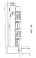
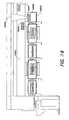
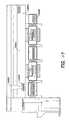
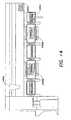
- FIG. 26shows a vertically arranged load lock and vertically stacked process modules in accordance with embodiments of the invention.
- FIG. 27shows a linearly arranged, two-level handling architecture with vertically stacked process modules in a cross-sectional side view in accordance with embodiments of the invention.
- FIG. 28shows the handling layout of FIG. 27 in a top view.
- FIG. 29shows an instrumented object on a robotic arm with sensors to detect proximity of the object to a target, in accordance with embodiments of the invention.
- FIG. 30illustrates how the movement of sensors over a target can allow the robotic arm to detect its position relative to the obstacle.
- FIG. 31shows how an instrumented object can use radio frequency communications in a vacuum environment to communicate position to a central controller.
- FIG. 32illustrates the output of a series of sensors as a function of position.
- FIGS. 33A-33Cshow a multi-shelf buffer for use in a batch processing system.
- FIG. 34shows an external return system for a handling system having a linear architecture.
- FIG. 34Ashows a U-shaped configuration for a linear handling system.
- FIG. 35shows certain details of an external return system for a handling system of FIG. 34 .
- FIG. 36shows additional details of an external return system for a handling system of FIG. 34 .
- FIG. 37shows movement of the output carrier in the return system of FIG. 34 .
- FIG. 38shows handling of an empty carrier in the return system of FIG. 34 .
- FIG. 39shows movement of the empty carrier in the return system of. FIG. 34 into a load lock position.
- FIG. 40shows the empty carrier lowered and evacuated and movement of the gripper in the return system of FIG. 34 .
- FIG. 41shows an empty carrier receiving material as a full carrier is being emptied in the return system of FIG. 34 .
- FIG. 42shows an empty carrier brought to a holding position, starting a new return cycle in the return system of FIG. 34 .
- FIG. 43shows an architecture for a handling facility for a manufacturing process, with a dual-arm robotic arm system and a return system in a linear architecture.
- FIG. 44shows an alternative embodiment of an overall system architecture for a handling method and system of the present invention.
- FIG. 45illustrates a fabrication facility including a mid-entry facility.
- FIG. 1shows a generalized layout of a semiconductor manufacturing system.
- the system 100may include one or more wafers 102 , a load lock 112 , one or more transfer robots 104 , one or more process modules 108 , one or more buffer modules 110 , and a plurality of slot valves 114 or other isolation valves for selectively isolated chambers of the system 100 , such as during various processing steps.
- the system 100operates to process wafers for use in, for example, semiconductor devices.
- Wafers 102may be moved from atmosphere to the vacuum environment through the load lock 112 for processing by the process modules 108 . It will be understood that, while the following description is generally directed to wafers, a variety of other objects may be handled within the system 100 including a production wafer, a test wafer, a cleaning wafer, a calibration wafer, or the like, as well as other substrates (such as for reticles, magnetic heads, flat panels, and the like), including square or rectangular substrates, that might usefully be processed in a vacuum or other controlled environment. All such workpieces are intended to fall within the scope of the term “wafer” as used herein unless a different meaning is explicitly provided or otherwise clear from the context.
- the transfer robots 104which may include robotic arms and the like, move wafers within the vacuum environment such as between process modules, or to and from the load lock 112 .
- the process modules 108may include any process modules suitable for use in a semiconductor manufacturing process.
- a process module 108includes at least one tool for processing a wafer 102 , such as tools for epitaxy, chemical vapor deposition, physical vapor deposition, etching, plasma processing, lithography, plating, cleaning, spin coating, and so forth.
- the particular tool or tools provided by a module 108are not important to the systems and methods disclosed herein, except to the extent that particular processes or tools have physical configuration requirements that constrain the module design 108 or wafer handling.
- references to a tool or process modulewill be understood to refer to any tool or process module suitable for use in a semiconductor manufacturing process unless a different meaning is explicitly provided or otherwise clear from the context.
- the process modules 108may have various widths, such as a standard width, a doublewide width, a stretched width, or the like.
- the widthmay be selected to accommodate other system components, such as two side-by-side transfer robot modules, two transfer robot modules separated by a buffer module, two transfer robot modules separated by a transfer station, or the like. It will be understood that the width may instead be selected to accommodate more robots, such as three robots, four robots, or more, either with or without buffers and/or transfer stations.
- a process module 108may accommodate a plurality of vacuum sub-chamber modules within the process module 108 , where access to the vacuum sub-chamber modules may be from a plurality of transfer robot modules through a plurality of isolation valves.
- Vacuum sub-chamber modulesmay also accommodate single wafers or groups of wafers. Each sub-chamber module may be individually controlled, to accommodate different processes running in different vacuum sub-chamber modules.
- a number of buffer modules 110may be employed in the system 100 to temporarily store wafers 102 , or facilitate transfer of wafers 102 between robots 104 .
- Buffer modules 110may be placed adjacent to a transfer robot module 104 , between two transfer robot modules 104 , between a transfer robot module 104 and an equipment front-end module (“EFEM”), between a plurality of robots 104 associated with modules, or the like.
- the buffer module 110may hold a plurality of wafers 102 , and the wafers 102 in the buffer module 110 may be accessed individually or in batches.
- the buffer module 110may also offer storage for a plurality of wafers 102 by incorporating a work piece elevator, or multi-level shelving (with suitable corresponding robotics). Wafers 102 may undergo a process step while in the buffer module 110 , such as heating, cooling, cleaning, testing, metrology, marking, handling, alignment, or the like.
- the load lock 112permits movement of wafers 102 into and out of the vacuum environment.
- a vacuum systemevacuates the load lock 112 before opening to a vacuum environment in the interior of the system, and vents the load lock 112 before opening to an exterior environment such as the atmosphere.
- the system 100may include a number of load locks at different locations, such as at the front of the system, back of the system, middle of the system, and the like. There may be a number of load locks 112 associated with one location within the system, such as multiple load locks 112 located at the front of the linear processing system.
- front-end load locks 112may have a dedicated robot and isolation valve associated with them for machine assisted loading and unloading of the system.
- These systemswhich may include EFEMs, front opening unified pods (“FOUPs”), and the like, are used to control wafer movement of wafers into and out of the vacuum processing environment.
- FOUPsfront opening unified pods
- the isolation valves 114are generally employed to isolate process modules during processing, or to otherwise isolate a portion of the vacuum environment from other interior regions. Isolation valves 114 may be placed between other components to temporarily isolate the environments of the system 100 , such as the interior chambers of process modules 108 during wafer processing. An isolation valve 114 may open and close, and provide a vacuum seal when closed. Isolation valves 114 may have a variety of sizes, and may control entrances that are serviced by one or more robots. A number of isolation valves 114 are described in greater detail below.
- the system 100may include a scanning electron microscope module, an ion implantation module, a flow through module, a multifunction module, a thermal bypass module, a vacuum extension module, a storage module, a transfer module, a metrology module, a heating or cooling station, or any other process module or the like.
- these modulesmay be vertically stacked, such as two load locks stacked one on top of the other, two process modules stacked one on top of the other, or the like.
- FIG. 1shows a particular arrangement of modules and so forth, that numerous combinations of process modules, robots, load locks, buffers, and the like may suitably be employed in a semiconductor manufacturing process.
- the components of the system 100may be changed, varied, and configured in numerous ways to accommodate different semiconductor processing schemes and customized to adapt to a unique function or group of functions. All such arrangements are intended to fall within this description.
- a number of process modulesare described below that may be used with a semiconductor processing system such as the system 100 described with reference to FIG. 1 .
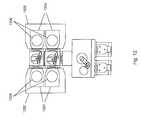
- FIG. 2shows a multi-wafer process module.
- the module 202may include a processing tool (not shown) for processing wafers 204 disposed in an interior thereof. Access to the interior may be through an entry 206 that includes an isolation valve or the like operable to selectively isolate the interior of the module 202 .
- a robot 208may be positioned outside the entry 206 , and adapted to place wafers 204 in the interior, or to retrieve the wafers 204 from the interior.
- the module 202is adapted to receive two wafers 204 side by side and substantially equidistant from the entry 206 and the robot 208 . In this arrangement, a clear access path is provided for the robot 208 to each wafer 204 , and the symmetry may advantageously simplify design of the module 202 .
- the size of the entry 206would be only wide enough and tall enough to accommodate a single wafer 204 , along with an end effector and any other portions of the robot that must pass into the interior during handling. This size may be optimized by having the robot 208 move wafers straight through a center of the entry 206 , which advantageously conserves valuable volume within the vacuum environment.
- the size of the wafer 204may vary. For example, while 300 mm is a conventional size for current wafers, new standards for semiconductor manufacturing provide for wafers over 400 mm in size.
- the shape and size of components (and voids) designed for wafer handlingmay vary, and one skilled in the art would understand how to adapt components such as the entry 206 to particular wafer dimensions.
- the entry 206may be positioned and sized to provide a straight-line path from the wafer's position within the module 202 and the wafer's position when at a center 210 of a chamber 212 housing the robot 208 . In other embodiments, the entry 206 may be positioned and sized to provide a straight-line path from the wafer's position within the module 202 and a center axis of the robot 208 (which will vary according to the type of robotic arm employed).
- FIG. 3shows a multi-wafer process module.
- the module 302typically includes one or more tools to process wafers 304 therein.
- the three wafers 304may be oriented in a triangle.
- the entry 306may be shaped and sized for passage of a single wafer, or may be somewhat wider to accommodate different paths for wafer passage in and out of an interior of the module 302 .
- other arrangements of three wafers 304may be employed, including wafers spaced radially equidistant from a center 310 of a robot handling module 312 , or linearly in various configurations.
- the robot 308has z-axis or vertical movement capability, the wafer 304 closest to the entrance 306 must generally be placed in last and removed first.
- FIG. 4shows a multi-wafer process module.
- This module 402positions two wafers 404 in-line with the entry 406 , which may advantageously permit the robot 408 to employ a single linear motion for accessing both wafers 404 .
- FIG. 5shows a multi-wafer process module.
- This module 502includes a wafer handler 520 adapted to move wafers 504 within the module 502 .
- the wafer handler 520may operate in a lazy-Suzan configuration to rotate one of the wafers 504 nearest to the entry 512 .
- the wafer handler 520may also rotate wafers 504 on the rotating handler 520 (using, for example, individual motors or a planetary gear train) to maintain rotational alignment of each wafer relative to the module 502 .
- a rotating handleris one possible configuration for the handler 520 that advantageously provides a relatively simple mechanical configuration
- other arrangementsare also possible including a conveyer belt, a Ferris wheel, a vertical conveyer belt with shelves for wafers, an elevator, and so forth.
- any mechanical system suitable for accommodating loading of multiple wafers into the module 502and preferable systems that accommodate use of an entry 512 sized for a single wafer and/or systems that reduce the required reach of robots into the module, may be useful employed in a multi-wafer process module as described herein.
- FIG. 6shows a controller shared by a number of process modules.
- each process modulehas a controller adapted specifically for control of hardware within the process module.
- the system 600 of FIG. 6includes a plurality of process modules 602 which may be any of the process modules described above, and may perform identical, similar, or different processes from one another. As depicted, two of the modules 602 are placed side-by-side and share a controller 604 .
- the controller 604may control hardware for both of the side-by-side modules 602 , and provide an interface for external access/control.
- sensorsmay be associated with the modules 602 to provide data to the controller 604 , as well as to recognize when a module is attached to an integrated processing system.
- a shared controller 604which may be a generic controller suitable for use with many different types of modules 602 or a module-specific controller, advantageously conserves space around process modules 602 permitting denser configurations of various tools, and may reduce costs associated with providing a separate controller for each process module 602 .
- the modules 602may also, or instead, share facilities such as a gas supply, exhaust(s), water, air, electricity, and the like.
- the shared controller 604may control shared facilities coupled to the modules 602 .
- FIG. 7shows two robotic arms sharing a buffer.
- two robots 702transfer wafers via a buffer 704 .
- no isolation valvesare employed between the robots 702 and/or the buffer 704 .
- This arrangementmay advantageously reduce or eliminate the need for direct robot-to-robot hand offs (due to the buffer 704 ), and permit closer spacing of robots 702 because no spacing is required for isolation valves.
- the buffer 704may include multiple shelves or other hardware for temporary storage of wafers.
- the buffer 704has a number of vertically stacked shelves, and remains stationary while robotic arms 702 move vertically to pick and place on different shelves.
- the buffer 704has a number of vertically stacked shelves, and the buffer 704 moves vertically to bring a specific shelf to the height of one of the robots 702 .
- each robotmay have an end effector or the like with a different elevation so that both robots 702 can access the buffer 704 simultaneously without collision.
- the end effectors of different robots 702may have complementary shapes to accommodate simultaneous linear access, or may have offset linear positions so that fingers of each end effector do not collide when both robots 702 are accessing the buffer 704 . More generally, it will be appreciated that numerous physical arrangements may be devised for a robotic system 700 that includes two or more robots 702 sharing a buffer 704 within a single isolation chamber. In other embodiments, two or more buffers 704 may also be employed. Each robot may also have multiple end effectors stacked vertically, which allows the robot to transfer multiple wafers simultaneously.
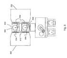
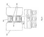
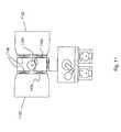
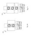
- FIG. 8shows a layout for dual-entry process modules.
- double-wide process modules 802include two different entries 804 , each having an isolation valve for selectively coupling an interior of the process module 802 to an external environment.
- the external environment of FIG. 8includes a single volume 806 (i.e., a shared or common environment without isolation valves) that contains two robots 808 and a buffer 810 .
- the robots 808may hand off to one another using shelves or the like within the buffer 810 , as generally described above. It will be understood that the robots 808 may also, or instead, directly hand off to one another.
- Each process module 802may concurrently hold and process a number of wafers, such as two wafers, three wafers, four wafers, and so forth. It will be readily understood that two wafers may be directly accessed by the two robots 808 and entries 804 , permitting parallel handling of wafers through the side-by-side entries 804 . Thus, for example, two wafers (or more wafers using, e.g., batch end effectors or the like), may be simultaneously transferred from the process module 802 depicted on the left of FIG. 8 and the process module 802 depicted on the right of FIG. 8 .
- the dual processing chambermay advantageously employ shared facilities, such as gasses, vacuum, water, electrical, and the like, which may reduce cost and overall footprint.
- This arrangementmay be particularly useful for a module 802 having long process times (for example, in the range of several minutes) by permitting concurrent processing and/or handling of multiple wafers.
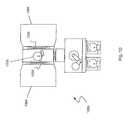
- FIG. 9shows a layout for a dual-entry process module.
- the robotic handlersare in chambers 902 isolated from one another by a buffer 904 with isolation valves 906 .
- This configuration of roboticsprovides significant advantages.
- the buffer 904may be isolated to accommodate interim processing steps such as metrology or alignment, and may physically accommodate more wafers.
- this arrangementpermits one of the robotic handlers to access a load lock/EFEM in isolation from the other robotic handler and process modules.
- this configurationrequires greater separation between the robotic handlers, and requires a correspondingly wider process module 908 .
- various internal transport mechanismsmay be provided within the process module 908 to permit movement of wafers within the module to a position close to the entry or entries.
- the process module 908may only process two wafers simultaneously.
- FIGS. 8-9may be readily adapted to accommodate three, four, or more entries with suitable modifications to entries, modules, and robotics. All such variations are intended to fall within the scope of this disclosure. As with other process modules described herein, these modules may also be readily adapted to batch processing by providing, for example, vertically stacked shelves and robots with dual or other multiple end effectors.
- FIG. 10shows a process module with an over-sized entry.
- an entry 1002 to a process module 1004may be substantially wider than the diameter of wafers handled by the system 1000 .
- the increased width of the entry 1002 and a corresponding isolation valvepermits linear access by a robot 1006 to more of the space within an interior chamber of the process module 1004 .
- the entry 1002may have a width that is 50% greater than the diameter of a wafer, twice the diameter of a wafer, or more than twice the diameter of a wafer.
- the entry 1002has a width determined by clearance for linear robotic access (with a wafer) to predetermined positions within the process module 1004 , such as the corners of the module 1004 opposing the entry 1002 , or other positions within the module 1004 . While it is possible for robots to reach around corners and the like, linear access or substantially linear access simplifies robotic handling and requires less total length of links within a robotic arm. In one aspect, two such process modules 1004 may share a robotic handler, thereby permitting a high degree of flexibility in placement and retrieval motions for wafers among the modules 1004 .
- FIG. 11shows a dual entry process module.
- Each process module 1102may be a dual-entry process module having two entries as described, for example with reference to FIG. 9 above.
- a single robot 1104may service each entry 1106 of one or more of the process modules 1102 . Due to the long reach requirements, the robot 1104 may include a four-link SCARA arm, a combination of telescoping and SCARA components, or any other combination of robotic links suitable for reaching into each entry 1106 to place and retrieve wafers in the process module(s) 1102 .
- FIG. 12shows multi-process modules.
- a process module 1202may include two (or more) vacuum sub-chambers 1204 for independently processing wafers 1206 .
- Each vacuum sub-chamber 1204may be separated from the other by a wall or similar divider that forms two isolated interiors within the module 1202 .
- Each vacuum sub-chamber 1204may, for example include one or more independent processing tools and an independent vacuum environment in the corresponding interior chamber selectively isolated with an isolation valve.
- each sub-chamber 1204may include a shared tool that independently processes each wafer 1206 , so that a single environment is employed within the process module 1202 even through wafers are processed separately and/or independently.
- the isolation entries and/or isolation valvesmay be substantially coplanar, such as to abut linearly arranged robotic handlers or other planar surfaces of handling systems.
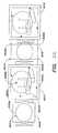
- FIG. 14shows multi-process modules.
- each process module 1402may include a number of entries 1404 for selective isolation of the processing environment within the process modules 1402 .
- the entries 1404 for each module 1402form planes that are angled with respect to one another. In one embodiment, these planes are oriented substantially normal to a ray from a wafer center within the module 1402 to a center of the robotic handler 1408 or a center axis of the robotic handler 1408 .
- This configurationprovides a number of advantages. For example, in this arrangement, a single robot 1408 may have linear access to each process module 1402 sub-chamber. Further, three process modules 1402 may be arranged around a single robot 1408 .
- this general configurationaffords the versatility of a cluster tool in combination with the modularity of individual process modules. It will be understood that while FIG. 14 depicts each entry 1404 as servicing a single sub-chamber within a process module 1402 , the process module 1402 may have a single, common interior where multiple wafers are exposed to a single process.
- FIG. 15shows an in-line process module in a layout.
- each linear process module 1502includes two entries 1504 on substantially opposite sides of the module 1502 .
- This configurationfacilitates linear arrangements of modules by permitting a wafer to be passed into the module 1502 on one side, processed with a tool (which may be, for example, any of the tools described above, and retrieved from the module 1502 on an opposing side so that multiple linear modules 1502 and/or other modules may be linked together in a manner that effectively permits processing during transport from one EFEM 1506 (or the like) to another EFEM 1508 .
- a toolwhich may be, for example, any of the tools described above
- the in-line process modulesmay provide processes used for all wafers in the system 1500 , while the other process modules may provide optional processes used only on some of the wafers.
- this layoutpermits use of a common system for different processes having partially similar processing requirements.
- FIG. 16shows a layout using dual entry process modules.
- two dual-entry process modulesshare a robotic handling system with a conventional, single process module.
- the dual-entry process modulesmay implement relatively long processes, while the conventional module provides a single, short process.
- the roboticsmay quickly transfer a series of wafers between the buffer and the short process module while a number of wafers are being processed in the dual entry process modules.
- FIG. 17shows a layout using dual entry process modules.
- this system 1700two additional process modules are added. This may be useful, for example, to balance the duty cycles of various process modules thereby providing higher utilization of each module, or provide for more efficient integration of relatively fast and slow processes or process modules within a single environment.
- FIG. 18shows a process module containing a scanning electron microscope.
- the system 1800may include an EFEM or FOUP 1802 , an entry 1804 including an isolation valve, a robotic handler 1806 , and a scanning electron microscope 1808 .
- the entry 1804may provide selective isolation to the robotic handler 1806 and/or microscope 1808 , and the robotic handler 1806 may transfer wafers between the microscope 1808 and the rest of the system 1800 .
- This general configurationmay be employed to add a scanning electron microscope to a semiconductor manufacturing system in a manner similar to any other process module, which advantageously permits microscopic inspection of wafers without removing wafers from the vacuum environment, or to add a stand-alone microscope to a vacuum environment fabrication facility
- FIG. 19shows a process module containing an ion implantation system.
- the system 1900may include an EFEM or FOUP 1902 , an entry 1904 including an isolation valve, a robotic handler 1906 , and an ion implantation system 1908 .
- the entry 1904may provide selective isolation to the robotic handler 1906 and/or ion implantation system 1908 , and the robotic handler 1906 may transfer wafers between the ion implantation system 1908 and the rest of the system 1900 .
- This general configurationmay be employed to add an ion implantation tool to a semiconductor manufacturing system in a manner similar to any other process module, which advantageously permits ion implantation on wafers without removing wafers from the vacuum environment, or to add a stand-alone implantation system to a vacuum environment fabrication facility.
- FIG. 20shows a layout using a scanning electron microscope module.
- the system 2000includes a scanning electron microscope module 2002 with an integrated transfer robot 2004 .
- This hardwareis incorporated into the semiconductor processing system 2000 , including additional transfer robotics, process modules, and EFEM. Such an embodiment may be useful for handling and setup of a microscopic scanning function within a vacuum processing environment, allowing the semiconductor work piece to be kept in vacuum throughout the process, including intermittent or final inspection using electron microscopy.
- the illustrated system 2000includes two dual-entry process modules as additional processing hardware, it will be understood that any suitable combination of process modules may be employed with the systems described herein.
- FIG. 21shows a layout using an ion implantation module.
- the system 2100includes an ion implantation system 2102 and two robotic handlers 2104 .
- This hardwareis incorporated into the semiconductor processing system 2100 , which includes additional transfer robotics, process modules, and two EFEMs.
- Such an embodimentmay be useful for handling and setup of ion implantation within a vacuum-processing environment, allowing the wafer to be kept in vacuum throughout a multi-step process that includes one or more ion implantation steps.
- the process systemis configured such that wafers that do not require ion implantation may bypass the ion implantation system through two robots and a buffer. Such a wafer may nonetheless be processed in other process modules connected to the system 2100 .
- a linear process module 2106may also be provided. This configuration may be particularly useful in high-throughput processes so that a bottleneck is avoided at either entry to or exit from the vacuum environment. In addition, the linear process module 2106 may be simultaneously or nearly simultaneously loaded from one entry while being unloaded from the other entry.
- FIG. 22illustrates a fabrication facility including a series of sensors 35002 .
- sensors 35002are commonly used to detect whether a material 35014 is still present on a robotic arm 35018 .
- Such sensors 35002may be commonly placed at each vacuum chamber 4012 entry and exit point.
- Such sensors 35002may consist of a vertical optical beam, either employing an emitter and detector, or employing a combination emitter/detector and a reflector.
- the training of robotic stationsis commonly accomplished by a skilled operator who views the position of the robot arm and materials and adjusts the robot position to ensure that the material 35014 is deposited in the correct location.
- frequently these positionsare very difficult to observe, and parallax and other optical problems present significant obstacles in properly training a robotic system.
- a training procedurecan consume many hours of equipment downtime.
- a series of sensors 35002 - 35010may include horizontal sensors 35004 - 35010 and vertical sensors 35002 .
- This combination of sensors 35002 - 35010may allow detection, for example through optical beam breaking, of either a robotic end effector, arm, or a handled object.
- the vertical sensor 35002may be placed slightly outside the area of the wafer 31008 when the robotic arm 3501 8 is in a retracted position.
- the vertical sensor 35002may also, or instead, be placed in a location such as a point 35012 within the wafer that is centered in front of the entrance opening and covered by the wafer when the robot is fully retracted. In this position the sensor may be able to tell the robotic controller that it has successfully picked up a wafer 31008 from a peripheral module.
- Horizontal sensors 35004 - 35010may also be advantageously employed.
- horizontal sensors 35004 - 35010are sometimes impractical due to the large diameter of the vacuum chamber, which may make alignment of the horizontal sensors 35004 - 35010 more complicated.
- the chamber sizemay be reduced significantly, thus may make it practical to include one or more horizontal sensors 35004 - 35010 .
- FIG. 23A-Cillustrates other possible locations of the horizontal sensors 35004 - 35010 and vertical sensors 35002 , such as straight across the chamber ( 36002 and 36008 ) and/or through mirrors 36006 placed inside the vacuum system.
- FIG. 24A-Billustrates a possible advantage of placing the sensor 35002 slightly outside the wafer 37001 radius when the robot arm is fully retracted.
- the sensor 35002detects the leading edge of the wafer 37001 at point “a” 37002 and the trailing edge at point “b” 37004 .
- These resultsmay indicate that the wafer 37001 was successfully retrieved, but by tying the sensor 35002 signal to the encoders, resolvers or other position elements present in the robotic drive, one can also calculate if the wafer 37001 is centered with respect to the end effector.
- the midpoint of the line segment “a-b” 37002 , 37004should correspond to the center of the end effector because of the circular geometry of a wafer 37001 . If the wafer 37001 slips on the end effector, inconsistent length measurements may reveal the slippage.
- a second line segment “c-d” 37008 , 37010may be detected when the wafer 37001 edges pass through the sensor. Again, the midpoint between “c” 37008 and “d” 37010 should coincide with the center of the end effector, and may permit a measurement or confirmation of wafer centering.
- the above methodmay allow the robot to detect the wafer 37001 as well as determine if the wafer 37001 is off-set from the expected location on the end effector.
- the combination of horizontal and vertical sensors 35002 - 35010may allow the system to be taught very rapidly using non-contact methods: the robotic arm and end effectors may be detected optically without the need for mechanical contact. Furthermore, the optical beams can be used during real-time wafer 37001 handling to verify that wafers 37001 are in the correct position during every wafer 37001 handling move.
- FIG. 25Ashows high-level components of a linear processing architecture 4000 for handling items in a manufacturing process.
- the architectureuses two or more stationary robots 4002 arranged in a linear fashion.
- the robots 4002can be either mounted in the bottom of the system or hang down from the chamber lid or both at the same time.
- the linear systemuses a vacuum chamber 4012 around the robot.
- the systemcould be comprised of multiple connected vacuum chambers 4012 , each with a vacuum chamber 4012 containing its own robot arranged in a linear fashion.
- a single controllercould be set up to handle one or more sections of the architecture.
- vacuum chambers 4012 sectionsare extensible; that is, a manufacturer can easily add additional sections/chambers 40 12 and thus add process capacity, much more easily than with cluster architectures.
- each sectionuses independent robot drives 4004 and arms 4002 , the throughput may stay high when additional sections and thus robots are added.
- cluster toolswhen the manufacturer adds process chambers 2002 , the system increases the load for the single robot, even if that robot is equipped with a dual arm, eventually the speed of the robot can become the limiting factor.
- systemsaddress this problem by adding additional robot arms 4002 into a single drive.
- Other manufacturershave used a 4-axis robot with two completely independent arms such as a dual SCARA or dual Frog-leg robots.
- the linear system disclosed hereinmay not be limited by robot capacity, since each section 4012 contains a robot, so each section 4012 is able to transport a much larger volume of material than with cluster tools.
- FIG. 25Bshows a stacked vacuum load lock 4008 , 40004 for entering materials into a vacuum environment.
- One limiting factor on bringing wafers 31008 into a vacuum systemis the speed with which the load lock can be evacuated to high vacuum. If the load lock is pumped too fast, condensation may occur in the air in the load lock chamber, resulting in precipitation of nuclei on the wafer 31008 surfaces, which can result in particles and can cause defects or poor device performance.
- Cluster toolsmay employ two load locks side by side, each of which is alternately evacuated. The pumping speed of each load lock can thus be slower, resulting in improved performance of the system. With two load locks 4008 , 40004 in a vertical stack, the equipment footprint stays very small, but retains the benefit of slower pumping speed.
- the load lock 40004can be added as an option.
- the robotic arms 4004 and 40006can each access either one of the two load locks 4008 , 40004 .
- the remaining handoff module 7008could be a single level handoff module.
- FIG. 25Cshows another load lock layout.
- wafers 31008can be entered and can exit at two levels on either side of the system, but follow a shared level in the rest of the system.
- FIG. 26details how the previous concept of stacked load locks 4008 , 40004 can be also implemented throughout a process by stacking two process modules 41006 , 41008 . Although such modules would not be compliant with the SEMI standard, such an architecture may offer significant benefits in equipment footprint and throughput.
- FIG. 27shows a system with two handling levels 4008 , 40004 , 4010 , 42004 : wafers may be independently transported between modules using either the top link 40006 or the bottom link 4004 .
- each handling levelmay have two load locks to provide the advantage of reduced evacuation speed noted above.
- a system with four input load locks, two handling levels, and optionally four output load locks,is also contemplated by description provided herein, as are systems with additional load lock and handling levels.
- FIG. 28shows a top view of the system of FIG. 27 .
- FIG. 29depicts a special instrumented object 44014 , such as a wafer.
- One or more sensors 44010may be integrated into the object 44014 , and may be able to detect environmental factors around the object 44014 .
- the sensors 44010may include proximity sensors such as capacitive, optical or magnetic proximity sensors.
- the sensors 44010may be connected to an amplifier/transmitter 44012 , which may use battery power to transmit radio frequency or other sensor signals, such as signals conforming to the 802.11b standard, to a receiver 44004 .
- the object 44014can be equipped with numerous sensors of different types and in different geometrically advantageous patterns.
- the sensors 1 through 6( 44010 ) are laid out in a radius equal to the radius of the target object 44008 .
- these sensorsare proximity sensors.
- By comparing the transient signals from the sensors 44010for example sensor 1 and sensor 6 , it can be determined if the object 44014 is approaching a target 44008 at the correct orientation. If the target 44008 is not approached correctly, one of the two sensors 44010 may show a premature trigger.
- the systemmay determine if the object 44010 is properly centered above the target 44008 before affecting a handoff.
- the sensors 44010can be arranged in any pattern according to, for example, efficiency of signal analysis or any other constraints. Radio frequency signals also advantageously operate in a vacuum environment.
- FIG. 30shows the system of , FIG. 29 in a side orientation illustrating the non-contact nature of orienting the instrumented object 44014 to a target 44008 .
- the sensors 44010may include other sensors for measuring properties of the target 44008 , such as temperature.
- FIG. 31depicts radio frequency communication with one or more sensors.
- a radio frequency sensor signal 440 16may be transmitted to an antenna 46002 within a vacuum. Appropriate selection of wavelengths may improve signal propagation with a fully metallic vacuum enclosure.
- the use of sensors in wireless communication with an external receiver and controllermay provide significant advantages. For example, this technique may reduce the time required for operations such as finding the center of a target, and information from the sensor(s) may be employed to provide visual feedback to an operator, or to automate certain operations using a robotic arm.
- the use of one or more sensorsmay permit measurements within the chamber that would otherwise require release of the vacuum to open to atmosphere and physically inspect the chamber. This may avoid costly or time consuming steps in conditioning the interior of the chamber, such as depressurization and baking (to drive out moisture or water vapor).
- FIG. 32illustrates the output from multiple sensors 44010 as a function of the robot movement.
- the motionmay result in the sensors providing information about, for example, distance to the target 44008 if the sensors are proximity sensors.
- the signalscan be individually or collectively analyzed to determine a location for the target 44008 relative to the sensors. Location or shape may be resolved in difference directions by moving the sensor(s) in two different directions and monitoring sensor signals, without physically contacting the target 44008 .
- FIG. 33A-Cillustrates how multiple transfer planes may be usefully employed to conserve floor space in a batch processing system.
- FIG. 33Ashows a linking module including multiple transfer planes to accommodate single or multiple access to wafers within the linking module. Slot valves or the like are provided to isolate the linking module.
- FIG. 33Bshows an alternative configuration in which multiple shelves are positioned between robots without isolation. In this configuration, the shelves may, for example, be positioned above the robots to permit a full range of robotic motion that might otherwise cause a collision between a robotic arm and wafers on the shelves. This configuration nonetheless provides batch processing and or multiple wafer buffering between robots.
- FIG. 33Cshows a top view of the embodiment of FIG. 33B . As visible in FIG.
- the small adapter with shelves between robots in FIG. 33Bpermits relatively close positioning of two robots without requiring direct robot-to-robot handoffs. Instead each wafer or group of wafers can be transferred to the elevated shelves for subsequent retrieval by an adjacent robot. As a significant advantage, this layout reduces the footprint of two adjacent robots while reducing or eliminating the extra complexity of coordinating direct robot-to-robot handoffs.
- FIG. 34shows an external return system for a handling system having a linear architecture 14000 .
- the return mechanismis optionally on the top of the linear vacuum chamber.
- the return pathis often through the same area as the entry path. This opens up the possibility of cross contamination, which occurs when clean wafers that are moving between process steps get contaminated by residuals entering the system from dirty wafers that are not yet cleaned. It also makes it necessary for the robot 4002 to handle materials going in as well as materials going out, and it makes it harder to control the vacuum environment.
- the air returnmay relatively cheap to implement; the air return may free up the vacuum robots 4002 because they do not have to handle materials going out; and the air return may keep clean finished materials out of the incoming areas, thereby lowering cross-contamination risks.
- Employing a small load lock 14010 in the rearmay add some costs, and so may the air tunnel 14012 , so in systems that are short and where vacuum levels and cross contamination are not so important, an air return may have less value, but in long systems with many integrated process steps the above-system air return could have significant benefits.
- the return systemcould also be a vacuum return, but that would be more expensive and more complicated to implement.
- a load lock 14010may be positioned at the end of a linear system, as depicted in FIG. 34 , the load lock 14010 could be positioned elsewhere, such as in the middle of the system.
- a manufacturing itemcould enter or exit the system at such another point in the system, such as to exit the system into the air return.
- the advantage of a mid-system exit pointmay be that in case of a partial system failure, materials or wafers can be recovered.
- the advantage of a mid-system entry pointmay be that wafers can be inserted in multiple places in the system, allowing for a significantly more flexible process flow.
- FIG. 34Ashows an example of a U-shaped linear system.
- an embodiment of the systemuses a dual carrier mechanism 14008 so that wafers that are finished can quickly be returned to the front of the system, but also so that an empty carrier 14008 can be placed where a full one was just removed.
- the air returnwill feature a carrier 14008 containing N wafers. N can be optimized depending on the throughput and cost requirements.
- the air return mechanismmay contain empty carriers 14008 so that when a full carrier 14018 is removed from the vacuum load lock 14010 , a new empty carrier 14008 can immediately be placed and load lock 14010 can evacuated to receive more materials.
- the air return mechanismmay be able to move wafers to the front of the system.
- a vertical lift 14004may be employed to lower the carrier to a level where the EFEM (Equipment Front End Module) robot can reach.
- the vertical lift 14004can lower to pick an empty carrier 14008 from the load lock.
- the air return mechanismmay feature a storage area 14014 for empty carriers 14008 , probably located at the very end and behind the location of the load lock 14010 .
- the gripper 14004can grip the carrier 14018 and move it forward slightly.
- the gripper 14004can then release the full carrier 14018 , move all the way back and retrieve an empty carrier 14008 , place it on the load lock 14010 .
- the load lock 14010can evacuate.
- the gripper 14004can now go back to the full carrier 14018 and move it all the way to the front of the system. Once the carrier 14018 has been emptied by the EFEM, it can be returned to the very back where it waits for the next cycle.
- FIG. 35shows certain additional details of an external return system for a handling system of FIG. 34 .
- FIG. 36shows additional details of an external return system for a handling system of FIG. 34 .
- FIG. 37shows movement of the output carrier 14018 in the return tunnel 14012 of FIG. 34 .
- the gripper 14004is shown in a position 17002 within the return tunnel 14012 away from the load lock 14010 . Once in the return tunnel 14012 the gripper 14004 may move to any available position 17012 within the return tunnel 14012 .
- FIG. 38shows handling of an empty carrier 14008 in the return system 14012 of FIG. 34 .
- FIG. 39shows movement of the empty carrier 14008 in the return tunnel 14012 of FIG. 34 into a load lock 14010 position.
- FIG. 40shows the empty carrier 14008 lowered and evacuated and movement of the gripper 14004 in the return system of FIG. 34 .
- FIG. 41shows an empty carrier 14008 receiving material as a full carrier 14018 is being emptied in the return tunnel 14012 of FIG. 34 .
- FIG. 42shows an empty carrier 14008 brought to a holding position, starting a new return cycle in the return tunnel 14012 of FIG. 34 .
- FIG. 43shows an architecture for a handling facility for a manufacturing process, with a dual-arm robotic arm system 23002 and a return system in a linear architecture.
- FIG. 44shows an alternative embodiment of an overall system architecture for a handling method and system of the present invention.
- FIG. 45illustrates a fabrication facility including a mid-entry point 33022 .
- the fabrication facilitymay include a load lock 14010 mid-stream 33002 where wafers 31008 can be taken out or entered.
- the air return system 14012can also take new wafers 31008 to the midpoint 33022 and enter wafers 31008 there.
- FIG. 12depicts two robots in a shared common environment handling wafers for the modules 1202 , a variety of other arrangements are possible.
- all of the entries 1204may be serviced by a single robot as described above with reference to FIG. 11 , or the entries 1204 may be serviced by a pair of robots separated by an isolated buffer as described above with reference to FIG. 9 .
- these conceptsmay be readily adapted to three entry or three process modules, or more generally, to any number of modules consistent with a particular fabrication facility or process.
- the devices disclosed hereinmay be combined in various ways within a semiconductor fabrication system, for example to form fabrication facilities adapted to balance processing load among relatively fast and relatively slow processes, or between processes amenable to batch processing and processes that are dedicated to a single wafer.
- fabrication facilitiesadapted to balance processing load among relatively fast and relatively slow processes, or between processes amenable to batch processing and processes that are dedicated to a single wafer.
Landscapes
- Engineering & Computer Science (AREA)
- Physics & Mathematics (AREA)
- Condensed Matter Physics & Semiconductors (AREA)
- General Physics & Mathematics (AREA)
- Manufacturing & Machinery (AREA)
- Computer Hardware Design (AREA)
- Microelectronics & Electronic Packaging (AREA)
- Power Engineering (AREA)
- Mechanical Engineering (AREA)
- Robotics (AREA)
- Container, Conveyance, Adherence, Positioning, Of Wafer (AREA)
Abstract
Description
Claims (15)
Priority Applications (2)
| Application Number | Priority Date | Filing Date | Title |
|---|---|---|---|
| US11/876,915US8313277B2 (en) | 2003-11-10 | 2007-10-23 | Semiconductor manufacturing process modules |
| US13/616,683US8870514B2 (en) | 2003-11-10 | 2012-09-14 | Semiconductor manufacturing process module |
Applications Claiming Priority (7)
| Application Number | Priority Date | Filing Date | Title |
|---|---|---|---|
| US51882303P | 2003-11-10 | 2003-11-10 | |
| US60764904P | 2004-09-07 | 2004-09-07 | |
| US10/985,834US7458763B2 (en) | 2003-11-10 | 2004-11-10 | Mid-entry load lock for semiconductor handling system |
| US77744306P | 2006-02-27 | 2006-02-27 | |
| US11/679,829US20070269297A1 (en) | 2003-11-10 | 2007-02-27 | Semiconductor wafer handling and transport |
| US11/681,978US20070286710A1 (en) | 2003-11-10 | 2007-03-05 | Semiconductor manufacturing process modules |
| US11/876,915US8313277B2 (en) | 2003-11-10 | 2007-10-23 | Semiconductor manufacturing process modules |
Related Parent Applications (2)
| Application Number | Title | Priority Date | Filing Date |
|---|---|---|---|
| US11/679,829Continuation-In-PartUS20070269297A1 (en) | 2003-11-10 | 2007-02-27 | Semiconductor wafer handling and transport |
| US11/681,978ContinuationUS20070286710A1 (en) | 2003-11-10 | 2007-03-05 | Semiconductor manufacturing process modules |
Related Child Applications (1)
| Application Number | Title | Priority Date | Filing Date |
|---|---|---|---|
| US13/616,683ContinuationUS8870514B2 (en) | 2003-11-10 | 2012-09-14 | Semiconductor manufacturing process module |
Publications (2)
| Publication Number | Publication Date |
|---|---|
| US20080124197A1 US20080124197A1 (en) | 2008-05-29 |
| US8313277B2true US8313277B2 (en) | 2012-11-20 |
Family
ID=46329541
Family Applications (2)
| Application Number | Title | Priority Date | Filing Date |
|---|---|---|---|
| US11/876,915Active2026-02-09US8313277B2 (en) | 2003-11-10 | 2007-10-23 | Semiconductor manufacturing process modules |
| US13/616,683Expired - LifetimeUS8870514B2 (en) | 2003-11-10 | 2012-09-14 | Semiconductor manufacturing process module |
Family Applications After (1)
| Application Number | Title | Priority Date | Filing Date |
|---|---|---|---|
| US13/616,683Expired - LifetimeUS8870514B2 (en) | 2003-11-10 | 2012-09-14 | Semiconductor manufacturing process module |
Country Status (1)
| Country | Link |
|---|---|
| US (2) | US8313277B2 (en) |
Cited By (13)
| Publication number | Priority date | Publication date | Assignee | Title |
|---|---|---|---|---|
| US20120014768A1 (en)* | 2010-07-13 | 2012-01-19 | Tokyo Electron Limited | Vacuum processing apparatus |
| US8897906B2 (en)* | 2011-08-23 | 2014-11-25 | Hitachi High-Technologies Corporation | Wafer processing based on sensor detection and system learning |
| US20180005907A1 (en)* | 2015-01-22 | 2018-01-04 | Lg Siltron Incorporated | Wafer transfer device |
| US20180286716A1 (en)* | 2017-03-31 | 2018-10-04 | Tokyo Electron Limited | Substrate Processing Apparatus |
| US10998209B2 (en) | 2019-05-31 | 2021-05-04 | Applied Materials, Inc. | Substrate processing platforms including multiple processing chambers |
| US11600507B2 (en) | 2020-09-09 | 2023-03-07 | Applied Materials, Inc. | Pedestal assembly for a substrate processing chamber |
| US11610799B2 (en) | 2020-09-18 | 2023-03-21 | Applied Materials, Inc. | Electrostatic chuck having a heating and chucking capabilities |
| US11674227B2 (en) | 2021-02-03 | 2023-06-13 | Applied Materials, Inc. | Symmetric pump down mini-volume with laminar flow cavity gas injection for high and low pressure |
| US11749542B2 (en) | 2020-07-27 | 2023-09-05 | Applied Materials, Inc. | Apparatus, system, and method for non-contact temperature monitoring of substrate supports |
| US11817331B2 (en) | 2020-07-27 | 2023-11-14 | Applied Materials, Inc. | Substrate holder replacement with protective disk during pasting process |
| US12002668B2 (en) | 2021-06-25 | 2024-06-04 | Applied Materials, Inc. | Thermal management hardware for uniform temperature control for enhanced bake-out for cluster tool |
| US12080571B2 (en) | 2020-07-08 | 2024-09-03 | Applied Materials, Inc. | Substrate processing module and method of moving a workpiece |
| US12195314B2 (en) | 2021-02-02 | 2025-01-14 | Applied Materials, Inc. | Cathode exchange mechanism to improve preventative maintenance time for cluster system |
Families Citing this family (399)
| Publication number | Priority date | Publication date | Assignee | Title |
|---|---|---|---|---|
| US20070269297A1 (en) | 2003-11-10 | 2007-11-22 | Meulen Peter V D | Semiconductor wafer handling and transport |
| US7458763B2 (en)* | 2003-11-10 | 2008-12-02 | Blueshift Technologies, Inc. | Mid-entry load lock for semiconductor handling system |
| US10086511B2 (en) | 2003-11-10 | 2018-10-02 | Brooks Automation, Inc. | Semiconductor manufacturing systems |
| US10378106B2 (en) | 2008-11-14 | 2019-08-13 | Asm Ip Holding B.V. | Method of forming insulation film by modified PEALD |
| US9394608B2 (en) | 2009-04-06 | 2016-07-19 | Asm America, Inc. | Semiconductor processing reactor and components thereof |
| US8802201B2 (en) | 2009-08-14 | 2014-08-12 | Asm America, Inc. | Systems and methods for thin-film deposition of metal oxides using excited nitrogen-oxygen species |
| US9004788B2 (en)* | 2010-06-08 | 2015-04-14 | Tokyo Electron Limited | Substrate processing apparatus, substrate processing method, and storage medium |
| US9312155B2 (en) | 2011-06-06 | 2016-04-12 | Asm Japan K.K. | High-throughput semiconductor-processing apparatus equipped with multiple dual-chamber modules |
| US9793148B2 (en) | 2011-06-22 | 2017-10-17 | Asm Japan K.K. | Method for positioning wafers in multiple wafer transport |
| US10364496B2 (en) | 2011-06-27 | 2019-07-30 | Asm Ip Holding B.V. | Dual section module having shared and unshared mass flow controllers |
| US10854498B2 (en) | 2011-07-15 | 2020-12-01 | Asm Ip Holding B.V. | Wafer-supporting device and method for producing same |
| US20130023129A1 (en) | 2011-07-20 | 2013-01-24 | Asm America, Inc. | Pressure transmitter for a semiconductor processing environment |
| US9017481B1 (en) | 2011-10-28 | 2015-04-28 | Asm America, Inc. | Process feed management for semiconductor substrate processing |
| US8946830B2 (en) | 2012-04-04 | 2015-02-03 | Asm Ip Holdings B.V. | Metal oxide protective layer for a semiconductor device |
| US9558931B2 (en) | 2012-07-27 | 2017-01-31 | Asm Ip Holding B.V. | System and method for gas-phase sulfur passivation of a semiconductor surface |
| US9659799B2 (en) | 2012-08-28 | 2017-05-23 | Asm Ip Holding B.V. | Systems and methods for dynamic semiconductor process scheduling |
| US10026044B1 (en) | 2012-09-10 | 2018-07-17 | Amazon Technologies, Inc. | System and method for arranging an order |
| US9021985B2 (en) | 2012-09-12 | 2015-05-05 | Asm Ip Holdings B.V. | Process gas management for an inductively-coupled plasma deposition reactor |
| US9324811B2 (en) | 2012-09-26 | 2016-04-26 | Asm Ip Holding B.V. | Structures and devices including a tensile-stressed silicon arsenic layer and methods of forming same |
| US9663293B2 (en)* | 2012-10-08 | 2017-05-30 | Amazon Technologies, Inc. | Replenishing a retail facility |
| US10714315B2 (en) | 2012-10-12 | 2020-07-14 | Asm Ip Holdings B.V. | Semiconductor reaction chamber showerhead |
| KR102143966B1 (en)* | 2012-12-03 | 2020-08-13 | 에이에스엠 아이피 홀딩 비.브이. | Modular vertical furnace processing system |
| US9640416B2 (en)* | 2012-12-26 | 2017-05-02 | Asm Ip Holding B.V. | Single-and dual-chamber module-attachable wafer-handling chamber |
| US20160376700A1 (en) | 2013-02-01 | 2016-12-29 | Asm Ip Holding B.V. | System for treatment of deposition reactor |
| US9484191B2 (en) | 2013-03-08 | 2016-11-01 | Asm Ip Holding B.V. | Pulsed remote plasma method and system |
| US9589770B2 (en) | 2013-03-08 | 2017-03-07 | Asm Ip Holding B.V. | Method and systems for in-situ formation of intermediate reactive species |
| US8993054B2 (en) | 2013-07-12 | 2015-03-31 | Asm Ip Holding B.V. | Method and system to reduce outgassing in a reaction chamber |
| US9018111B2 (en) | 2013-07-22 | 2015-04-28 | Asm Ip Holding B.V. | Semiconductor reaction chamber with plasma capabilities |
| US9793115B2 (en) | 2013-08-14 | 2017-10-17 | Asm Ip Holding B.V. | Structures and devices including germanium-tin films and methods of forming same |
| US9240412B2 (en) | 2013-09-27 | 2016-01-19 | Asm Ip Holding B.V. | Semiconductor structure and device and methods of forming same using selective epitaxial process |
| US9556516B2 (en) | 2013-10-09 | 2017-01-31 | ASM IP Holding B.V | Method for forming Ti-containing film by PEALD using TDMAT or TDEAT |
| US10179947B2 (en) | 2013-11-26 | 2019-01-15 | Asm Ip Holding B.V. | Method for forming conformal nitrided, oxidized, or carbonized dielectric film by atomic layer deposition |
| US11587813B2 (en) | 2013-12-17 | 2023-02-21 | Brooks Automation Us, Llc | Substrate transport apparatus |
| US10683571B2 (en) | 2014-02-25 | 2020-06-16 | Asm Ip Holding B.V. | Gas supply manifold and method of supplying gases to chamber using same |
| US9447498B2 (en) | 2014-03-18 | 2016-09-20 | Asm Ip Holding B.V. | Method for performing uniform processing in gas system-sharing multiple reaction chambers |
| US10167557B2 (en) | 2014-03-18 | 2019-01-01 | Asm Ip Holding B.V. | Gas distribution system, reactor including the system, and methods of using the same |
| US11015245B2 (en) | 2014-03-19 | 2021-05-25 | Asm Ip Holding B.V. | Gas-phase reactor and system having exhaust plenum and components thereof |
| US9404587B2 (en) | 2014-04-24 | 2016-08-02 | ASM IP Holding B.V | Lockout tagout for semiconductor vacuum valve |
| US10858737B2 (en) | 2014-07-28 | 2020-12-08 | Asm Ip Holding B.V. | Showerhead assembly and components thereof |
| US9543180B2 (en) | 2014-08-01 | 2017-01-10 | Asm Ip Holding B.V. | Apparatus and method for transporting wafers between wafer carrier and process tool under vacuum |
| US9890456B2 (en) | 2014-08-21 | 2018-02-13 | Asm Ip Holding B.V. | Method and system for in situ formation of gas-phase compounds |
| US10941490B2 (en) | 2014-10-07 | 2021-03-09 | Asm Ip Holding B.V. | Multiple temperature range susceptor, assembly, reactor and system including the susceptor, and methods of using the same |
| US9657845B2 (en) | 2014-10-07 | 2017-05-23 | Asm Ip Holding B.V. | Variable conductance gas distribution apparatus and method |
| KR102300403B1 (en) | 2014-11-19 | 2021-09-09 | 에이에스엠 아이피 홀딩 비.브이. | Method of depositing thin film |
| KR102263121B1 (en) | 2014-12-22 | 2021-06-09 | 에이에스엠 아이피 홀딩 비.브이. | Semiconductor device and manufacuring method thereof |
| US9478415B2 (en) | 2015-02-13 | 2016-10-25 | Asm Ip Holding B.V. | Method for forming film having low resistance and shallow junction depth |
| US10529542B2 (en) | 2015-03-11 | 2020-01-07 | Asm Ip Holdings B.V. | Cross-flow reactor and method |
| US10276355B2 (en) | 2015-03-12 | 2019-04-30 | Asm Ip Holding B.V. | Multi-zone reactor, system including the reactor, and method of using the same |
| US10458018B2 (en) | 2015-06-26 | 2019-10-29 | Asm Ip Holding B.V. | Structures including metal carbide material, devices including the structures, and methods of forming same |
| US10600673B2 (en) | 2015-07-07 | 2020-03-24 | Asm Ip Holding B.V. | Magnetic susceptor to baseplate seal |
| US10043661B2 (en) | 2015-07-13 | 2018-08-07 | Asm Ip Holding B.V. | Method for protecting layer by forming hydrocarbon-based extremely thin film |
| US9899291B2 (en) | 2015-07-13 | 2018-02-20 | Asm Ip Holding B.V. | Method for protecting layer by forming hydrocarbon-based extremely thin film |
| US10083836B2 (en) | 2015-07-24 | 2018-09-25 | Asm Ip Holding B.V. | Formation of boron-doped titanium metal films with high work function |
| US10087525B2 (en) | 2015-08-04 | 2018-10-02 | Asm Ip Holding B.V. | Variable gap hard stop design |
| US9647114B2 (en) | 2015-08-14 | 2017-05-09 | Asm Ip Holding B.V. | Methods of forming highly p-type doped germanium tin films and structures and devices including the films |
| US9711345B2 (en) | 2015-08-25 | 2017-07-18 | Asm Ip Holding B.V. | Method for forming aluminum nitride-based film by PEALD |
| JP2018529236A (en)* | 2015-09-22 | 2018-10-04 | アプライド マテリアルズ インコーポレイテッドApplied Materials,Incorporated | Large area dual substrate processing system |
| US9960072B2 (en) | 2015-09-29 | 2018-05-01 | Asm Ip Holding B.V. | Variable adjustment for precise matching of multiple chamber cavity housings |
| US9909214B2 (en) | 2015-10-15 | 2018-03-06 | Asm Ip Holding B.V. | Method for depositing dielectric film in trenches by PEALD |
| US10211308B2 (en) | 2015-10-21 | 2019-02-19 | Asm Ip Holding B.V. | NbMC layers |
| US10322384B2 (en) | 2015-11-09 | 2019-06-18 | Asm Ip Holding B.V. | Counter flow mixer for process chamber |
| US9455138B1 (en) | 2015-11-10 | 2016-09-27 | Asm Ip Holding B.V. | Method for forming dielectric film in trenches by PEALD using H-containing gas |
| US9905420B2 (en) | 2015-12-01 | 2018-02-27 | Asm Ip Holding B.V. | Methods of forming silicon germanium tin films and structures and devices including the films |
| US9607837B1 (en) | 2015-12-21 | 2017-03-28 | Asm Ip Holding B.V. | Method for forming silicon oxide cap layer for solid state diffusion process |
| US9735024B2 (en) | 2015-12-28 | 2017-08-15 | Asm Ip Holding B.V. | Method of atomic layer etching using functional group-containing fluorocarbon |
| US9627221B1 (en) | 2015-12-28 | 2017-04-18 | Asm Ip Holding B.V. | Continuous process incorporating atomic layer etching |
| US11139308B2 (en) | 2015-12-29 | 2021-10-05 | Asm Ip Holding B.V. | Atomic layer deposition of III-V compounds to form V-NAND devices |
| US9754779B1 (en) | 2016-02-19 | 2017-09-05 | Asm Ip Holding B.V. | Method for forming silicon nitride film selectively on sidewalls or flat surfaces of trenches |
| US10529554B2 (en) | 2016-02-19 | 2020-01-07 | Asm Ip Holding B.V. | Method for forming silicon nitride film selectively on sidewalls or flat surfaces of trenches |
| US10468251B2 (en) | 2016-02-19 | 2019-11-05 | Asm Ip Holding B.V. | Method for forming spacers using silicon nitride film for spacer-defined multiple patterning |
| US10501866B2 (en) | 2016-03-09 | 2019-12-10 | Asm Ip Holding B.V. | Gas distribution apparatus for improved film uniformity in an epitaxial system |
| US10343920B2 (en) | 2016-03-18 | 2019-07-09 | Asm Ip Holding B.V. | Aligned carbon nanotubes |
| US9892913B2 (en) | 2016-03-24 | 2018-02-13 | Asm Ip Holding B.V. | Radial and thickness control via biased multi-port injection settings |
| US10190213B2 (en) | 2016-04-21 | 2019-01-29 | Asm Ip Holding B.V. | Deposition of metal borides |
| US10087522B2 (en) | 2016-04-21 | 2018-10-02 | Asm Ip Holding B.V. | Deposition of metal borides |
| US10865475B2 (en) | 2016-04-21 | 2020-12-15 | Asm Ip Holding B.V. | Deposition of metal borides and silicides |
| US10367080B2 (en) | 2016-05-02 | 2019-07-30 | Asm Ip Holding B.V. | Method of forming a germanium oxynitride film |
| US10032628B2 (en) | 2016-05-02 | 2018-07-24 | Asm Ip Holding B.V. | Source/drain performance through conformal solid state doping |
| KR102592471B1 (en) | 2016-05-17 | 2023-10-20 | 에이에스엠 아이피 홀딩 비.브이. | Method of forming metal interconnection and method of fabricating semiconductor device using the same |
| US11453943B2 (en) | 2016-05-25 | 2022-09-27 | Asm Ip Holding B.V. | Method for forming carbon-containing silicon/metal oxide or nitride film by ALD using silicon precursor and hydrocarbon precursor |
| US10388509B2 (en) | 2016-06-28 | 2019-08-20 | Asm Ip Holding B.V. | Formation of epitaxial layers via dislocation filtering |
| US10612137B2 (en) | 2016-07-08 | 2020-04-07 | Asm Ip Holdings B.V. | Organic reactants for atomic layer deposition |
| US9859151B1 (en) | 2016-07-08 | 2018-01-02 | Asm Ip Holding B.V. | Selective film deposition method to form air gaps |
| US9793135B1 (en) | 2016-07-14 | 2017-10-17 | ASM IP Holding B.V | Method of cyclic dry etching using etchant film |
| US10714385B2 (en) | 2016-07-19 | 2020-07-14 | Asm Ip Holding B.V. | Selective deposition of tungsten |
| KR102354490B1 (en) | 2016-07-27 | 2022-01-21 | 에이에스엠 아이피 홀딩 비.브이. | Method of processing a substrate |
| US10177025B2 (en) | 2016-07-28 | 2019-01-08 | Asm Ip Holding B.V. | Method and apparatus for filling a gap |
| KR102532607B1 (en) | 2016-07-28 | 2023-05-15 | 에이에스엠 아이피 홀딩 비.브이. | Substrate processing apparatus and method of operating the same |
| US10395919B2 (en) | 2016-07-28 | 2019-08-27 | Asm Ip Holding B.V. | Method and apparatus for filling a gap |
| US9887082B1 (en) | 2016-07-28 | 2018-02-06 | Asm Ip Holding B.V. | Method and apparatus for filling a gap |
| US9812320B1 (en) | 2016-07-28 | 2017-11-07 | Asm Ip Holding B.V. | Method and apparatus for filling a gap |
| JP6830772B2 (en)* | 2016-08-04 | 2021-02-17 | 株式会社ジャパンディスプレイ | Laminated film manufacturing equipment and laminated film manufacturing method |
| US10090316B2 (en) | 2016-09-01 | 2018-10-02 | Asm Ip Holding B.V. | 3D stacked multilayer semiconductor memory using doped select transistor channel |
| US10410943B2 (en) | 2016-10-13 | 2019-09-10 | Asm Ip Holding B.V. | Method for passivating a surface of a semiconductor and related systems |
| US10643826B2 (en) | 2016-10-26 | 2020-05-05 | Asm Ip Holdings B.V. | Methods for thermally calibrating reaction chambers |
| US11532757B2 (en) | 2016-10-27 | 2022-12-20 | Asm Ip Holding B.V. | Deposition of charge trapping layers |
| US10229833B2 (en) | 2016-11-01 | 2019-03-12 | Asm Ip Holding B.V. | Methods for forming a transition metal nitride film on a substrate by atomic layer deposition and related semiconductor device structures |
| US10643904B2 (en) | 2016-11-01 | 2020-05-05 | Asm Ip Holdings B.V. | Methods for forming a semiconductor device and related semiconductor device structures |
| US10714350B2 (en) | 2016-11-01 | 2020-07-14 | ASM IP Holdings, B.V. | Methods for forming a transition metal niobium nitride film on a substrate by atomic layer deposition and related semiconductor device structures |
| US10435790B2 (en) | 2016-11-01 | 2019-10-08 | Asm Ip Holding B.V. | Method of subatmospheric plasma-enhanced ALD using capacitively coupled electrodes with narrow gap |
| US10134757B2 (en) | 2016-11-07 | 2018-11-20 | Asm Ip Holding B.V. | Method of processing a substrate and a device manufactured by using the method |
| KR102546317B1 (en) | 2016-11-15 | 2023-06-21 | 에이에스엠 아이피 홀딩 비.브이. | Gas supply unit and substrate processing apparatus including the same |
| US10340135B2 (en) | 2016-11-28 | 2019-07-02 | Asm Ip Holding B.V. | Method of topologically restricted plasma-enhanced cyclic deposition of silicon or metal nitride |
| KR102762543B1 (en) | 2016-12-14 | 2025-02-05 | 에이에스엠 아이피 홀딩 비.브이. | Substrate processing apparatus |
| US11447861B2 (en) | 2016-12-15 | 2022-09-20 | Asm Ip Holding B.V. | Sequential infiltration synthesis apparatus and a method of forming a patterned structure |
| US9916980B1 (en) | 2016-12-15 | 2018-03-13 | Asm Ip Holding B.V. | Method of forming a structure on a substrate |
| US11581186B2 (en) | 2016-12-15 | 2023-02-14 | Asm Ip Holding B.V. | Sequential infiltration synthesis apparatus |
| KR102700194B1 (en) | 2016-12-19 | 2024-08-28 | 에이에스엠 아이피 홀딩 비.브이. | Substrate processing apparatus |
| US10269558B2 (en) | 2016-12-22 | 2019-04-23 | Asm Ip Holding B.V. | Method of forming a structure on a substrate |
| US10867788B2 (en) | 2016-12-28 | 2020-12-15 | Asm Ip Holding B.V. | Method of forming a structure on a substrate |
| US11390950B2 (en) | 2017-01-10 | 2022-07-19 | Asm Ip Holding B.V. | Reactor system and method to reduce residue buildup during a film deposition process |
| US10655221B2 (en) | 2017-02-09 | 2020-05-19 | Asm Ip Holding B.V. | Method for depositing oxide film by thermal ALD and PEALD |
| US10468261B2 (en) | 2017-02-15 | 2019-11-05 | Asm Ip Holding B.V. | Methods for forming a metallic film on a substrate by cyclical deposition and related semiconductor device structures |
| US10283353B2 (en) | 2017-03-29 | 2019-05-07 | Asm Ip Holding B.V. | Method of reforming insulating film deposited on substrate with recess pattern |
| US10529563B2 (en) | 2017-03-29 | 2020-01-07 | Asm Ip Holdings B.V. | Method for forming doped metal oxide films on a substrate by cyclical deposition and related semiconductor device structures |
| US10103040B1 (en) | 2017-03-31 | 2018-10-16 | Asm Ip Holding B.V. | Apparatus and method for manufacturing a semiconductor device |
| USD830981S1 (en) | 2017-04-07 | 2018-10-16 | Asm Ip Holding B.V. | Susceptor for semiconductor substrate processing apparatus |
| KR102457289B1 (en) | 2017-04-25 | 2022-10-21 | 에이에스엠 아이피 홀딩 비.브이. | Method for depositing a thin film and manufacturing a semiconductor device |
| US10446393B2 (en) | 2017-05-08 | 2019-10-15 | Asm Ip Holding B.V. | Methods for forming silicon-containing epitaxial layers and related semiconductor device structures |
| US10770286B2 (en) | 2017-05-08 | 2020-09-08 | Asm Ip Holdings B.V. | Methods for selectively forming a silicon nitride film on a substrate and related semiconductor device structures |
| US10892156B2 (en) | 2017-05-08 | 2021-01-12 | Asm Ip Holding B.V. | Methods for forming a silicon nitride film on a substrate and related semiconductor device structures |
| US10504742B2 (en) | 2017-05-31 | 2019-12-10 | Asm Ip Holding B.V. | Method of atomic layer etching using hydrogen plasma |
| US10886123B2 (en) | 2017-06-02 | 2021-01-05 | Asm Ip Holding B.V. | Methods for forming low temperature semiconductor layers and related semiconductor device structures |
| US12040200B2 (en) | 2017-06-20 | 2024-07-16 | Asm Ip Holding B.V. | Semiconductor processing apparatus and methods for calibrating a semiconductor processing apparatus |
| US11306395B2 (en) | 2017-06-28 | 2022-04-19 | Asm Ip Holding B.V. | Methods for depositing a transition metal nitride film on a substrate by atomic layer deposition and related deposition apparatus |
| US10685834B2 (en) | 2017-07-05 | 2020-06-16 | Asm Ip Holdings B.V. | Methods for forming a silicon germanium tin layer and related semiconductor device structures |
| KR20190009245A (en) | 2017-07-18 | 2019-01-28 | 에이에스엠 아이피 홀딩 비.브이. | Methods for forming a semiconductor device structure and related semiconductor device structures |
| US10541333B2 (en) | 2017-07-19 | 2020-01-21 | Asm Ip Holding B.V. | Method for depositing a group IV semiconductor and related semiconductor device structures |
| US11374112B2 (en) | 2017-07-19 | 2022-06-28 | Asm Ip Holding B.V. | Method for depositing a group IV semiconductor and related semiconductor device structures |
| US11018002B2 (en) | 2017-07-19 | 2021-05-25 | Asm Ip Holding B.V. | Method for selectively depositing a Group IV semiconductor and related semiconductor device structures |
| US10605530B2 (en) | 2017-07-26 | 2020-03-31 | Asm Ip Holding B.V. | Assembly of a liner and a flange for a vertical furnace as well as the liner and the vertical furnace |
| US10590535B2 (en) | 2017-07-26 | 2020-03-17 | Asm Ip Holdings B.V. | Chemical treatment, deposition and/or infiltration apparatus and method for using the same |
| US10312055B2 (en) | 2017-07-26 | 2019-06-04 | Asm Ip Holding B.V. | Method of depositing film by PEALD using negative bias |
| TWI815813B (en) | 2017-08-04 | 2023-09-21 | 荷蘭商Asm智慧財產控股公司 | Showerhead assembly for distributing a gas within a reaction chamber |
| US10692741B2 (en) | 2017-08-08 | 2020-06-23 | Asm Ip Holdings B.V. | Radiation shield |
| US10770336B2 (en) | 2017-08-08 | 2020-09-08 | Asm Ip Holding B.V. | Substrate lift mechanism and reactor including same |
| US10249524B2 (en) | 2017-08-09 | 2019-04-02 | Asm Ip Holding B.V. | Cassette holder assembly for a substrate cassette and holding member for use in such assembly |
| US11139191B2 (en) | 2017-08-09 | 2021-10-05 | Asm Ip Holding B.V. | Storage apparatus for storing cassettes for substrates and processing apparatus equipped therewith |
| US11769682B2 (en) | 2017-08-09 | 2023-09-26 | Asm Ip Holding B.V. | Storage apparatus for storing cassettes for substrates and processing apparatus equipped therewith |
| US10236177B1 (en) | 2017-08-22 | 2019-03-19 | ASM IP Holding B.V.. | Methods for depositing a doped germanium tin semiconductor and related semiconductor device structures |
| USD900036S1 (en) | 2017-08-24 | 2020-10-27 | Asm Ip Holding B.V. | Heater electrical connector and adapter |
| US11830730B2 (en) | 2017-08-29 | 2023-11-28 | Asm Ip Holding B.V. | Layer forming method and apparatus |
| US11056344B2 (en) | 2017-08-30 | 2021-07-06 | Asm Ip Holding B.V. | Layer forming method |
| US11295980B2 (en) | 2017-08-30 | 2022-04-05 | Asm Ip Holding B.V. | Methods for depositing a molybdenum metal film over a dielectric surface of a substrate by a cyclical deposition process and related semiconductor device structures |
| KR102491945B1 (en) | 2017-08-30 | 2023-01-26 | 에이에스엠 아이피 홀딩 비.브이. | Substrate processing apparatus |
| KR102401446B1 (en) | 2017-08-31 | 2022-05-24 | 에이에스엠 아이피 홀딩 비.브이. | Substrate processing apparatus |
| US10607895B2 (en) | 2017-09-18 | 2020-03-31 | Asm Ip Holdings B.V. | Method for forming a semiconductor device structure comprising a gate fill metal |
| KR102630301B1 (en) | 2017-09-21 | 2024-01-29 | 에이에스엠 아이피 홀딩 비.브이. | Method of sequential infiltration synthesis treatment of infiltrateable material and structures and devices formed using same |
| US10844484B2 (en) | 2017-09-22 | 2020-11-24 | Asm Ip Holding B.V. | Apparatus for dispensing a vapor phase reactant to a reaction chamber and related methods |
| US10658205B2 (en) | 2017-09-28 | 2020-05-19 | Asm Ip Holdings B.V. | Chemical dispensing apparatus and methods for dispensing a chemical to a reaction chamber |
| US10403504B2 (en) | 2017-10-05 | 2019-09-03 | Asm Ip Holding B.V. | Method for selectively depositing a metallic film on a substrate |
| US10319588B2 (en) | 2017-10-10 | 2019-06-11 | Asm Ip Holding B.V. | Method for depositing a metal chalcogenide on a substrate by cyclical deposition |
| US10923344B2 (en) | 2017-10-30 | 2021-02-16 | Asm Ip Holding B.V. | Methods for forming a semiconductor structure and related semiconductor structures |
| KR102443047B1 (en) | 2017-11-16 | 2022-09-14 | 에이에스엠 아이피 홀딩 비.브이. | Method of processing a substrate and a device manufactured by the same |
| US10910262B2 (en) | 2017-11-16 | 2021-02-02 | Asm Ip Holding B.V. | Method of selectively depositing a capping layer structure on a semiconductor device structure |
| US11022879B2 (en) | 2017-11-24 | 2021-06-01 | Asm Ip Holding B.V. | Method of forming an enhanced unexposed photoresist layer |
| CN111344522B (en) | 2017-11-27 | 2022-04-12 | 阿斯莫Ip控股公司 | Including clean mini-environment device |
| WO2019103613A1 (en) | 2017-11-27 | 2019-05-31 | Asm Ip Holding B.V. | A storage device for storing wafer cassettes for use with a batch furnace |
| US10290508B1 (en) | 2017-12-05 | 2019-05-14 | Asm Ip Holding B.V. | Method for forming vertical spacers for spacer-defined patterning |
| US10872771B2 (en) | 2018-01-16 | 2020-12-22 | Asm Ip Holding B. V. | Method for depositing a material film on a substrate within a reaction chamber by a cyclical deposition process and related device structures |
| TWI799494B (en) | 2018-01-19 | 2023-04-21 | 荷蘭商Asm 智慧財產控股公司 | Deposition method |
| KR102695659B1 (en) | 2018-01-19 | 2024-08-14 | 에이에스엠 아이피 홀딩 비.브이. | Method for depositing a gap filling layer by plasma assisted deposition |
| USD903477S1 (en) | 2018-01-24 | 2020-12-01 | Asm Ip Holdings B.V. | Metal clamp |
| US11018047B2 (en) | 2018-01-25 | 2021-05-25 | Asm Ip Holding B.V. | Hybrid lift pin |
| US10535516B2 (en) | 2018-02-01 | 2020-01-14 | Asm Ip Holdings B.V. | Method for depositing a semiconductor structure on a surface of a substrate and related semiconductor structures |
| USD880437S1 (en) | 2018-02-01 | 2020-04-07 | Asm Ip Holding B.V. | Gas supply plate for semiconductor manufacturing apparatus |
| US11081345B2 (en) | 2018-02-06 | 2021-08-03 | Asm Ip Holding B.V. | Method of post-deposition treatment for silicon oxide film |
| US10896820B2 (en) | 2018-02-14 | 2021-01-19 | Asm Ip Holding B.V. | Method for depositing a ruthenium-containing film on a substrate by a cyclical deposition process |
| WO2019158960A1 (en) | 2018-02-14 | 2019-08-22 | Asm Ip Holding B.V. | A method for depositing a ruthenium-containing film on a substrate by a cyclical deposition process |
| US10731249B2 (en) | 2018-02-15 | 2020-08-04 | Asm Ip Holding B.V. | Method of forming a transition metal containing film on a substrate by a cyclical deposition process, a method for supplying a transition metal halide compound to a reaction chamber, and related vapor deposition apparatus |
| US10658181B2 (en) | 2018-02-20 | 2020-05-19 | Asm Ip Holding B.V. | Method of spacer-defined direct patterning in semiconductor fabrication |
| KR102636427B1 (en) | 2018-02-20 | 2024-02-13 | 에이에스엠 아이피 홀딩 비.브이. | Substrate processing method and apparatus |
| US10975470B2 (en) | 2018-02-23 | 2021-04-13 | Asm Ip Holding B.V. | Apparatus for detecting or monitoring for a chemical precursor in a high temperature environment |
| US11473195B2 (en) | 2018-03-01 | 2022-10-18 | Asm Ip Holding B.V. | Semiconductor processing apparatus and a method for processing a substrate |
| US11629406B2 (en) | 2018-03-09 | 2023-04-18 | Asm Ip Holding B.V. | Semiconductor processing apparatus comprising one or more pyrometers for measuring a temperature of a substrate during transfer of the substrate |
| US11114283B2 (en) | 2018-03-16 | 2021-09-07 | Asm Ip Holding B.V. | Reactor, system including the reactor, and methods of manufacturing and using same |
| KR102646467B1 (en) | 2018-03-27 | 2024-03-11 | 에이에스엠 아이피 홀딩 비.브이. | Method of forming an electrode on a substrate and a semiconductor device structure including an electrode |
| US11230766B2 (en) | 2018-03-29 | 2022-01-25 | Asm Ip Holding B.V. | Substrate processing apparatus and method |
| US11088002B2 (en) | 2018-03-29 | 2021-08-10 | Asm Ip Holding B.V. | Substrate rack and a substrate processing system and method |
| US10510536B2 (en) | 2018-03-29 | 2019-12-17 | Asm Ip Holding B.V. | Method of depositing a co-doped polysilicon film on a surface of a substrate within a reaction chamber |
| KR102501472B1 (en) | 2018-03-30 | 2023-02-20 | 에이에스엠 아이피 홀딩 비.브이. | Substrate processing method |
| KR102600229B1 (en) | 2018-04-09 | 2023-11-10 | 에이에스엠 아이피 홀딩 비.브이. | Substrate supporting device, substrate processing apparatus including the same and substrate processing method |
| US12025484B2 (en) | 2018-05-08 | 2024-07-02 | Asm Ip Holding B.V. | Thin film forming method |
| TWI811348B (en) | 2018-05-08 | 2023-08-11 | 荷蘭商Asm 智慧財產控股公司 | Methods for depositing an oxide film on a substrate by a cyclical deposition process and related device structures |
| US12272527B2 (en) | 2018-05-09 | 2025-04-08 | Asm Ip Holding B.V. | Apparatus for use with hydrogen radicals and method of using same |
| KR20190129718A (en) | 2018-05-11 | 2019-11-20 | 에이에스엠 아이피 홀딩 비.브이. | Methods for forming a doped metal carbide film on a substrate and related semiconductor device structures |
| KR102596988B1 (en) | 2018-05-28 | 2023-10-31 | 에이에스엠 아이피 홀딩 비.브이. | Method of processing a substrate and a device manufactured by the same |
| US11718913B2 (en) | 2018-06-04 | 2023-08-08 | Asm Ip Holding B.V. | Gas distribution system and reactor system including same |
| TWI840362B (en) | 2018-06-04 | 2024-05-01 | 荷蘭商Asm Ip私人控股有限公司 | Wafer handling chamber with moisture reduction |
| US11286562B2 (en) | 2018-06-08 | 2022-03-29 | Asm Ip Holding B.V. | Gas-phase chemical reactor and method of using same |
| US10797133B2 (en) | 2018-06-21 | 2020-10-06 | Asm Ip Holding B.V. | Method for depositing a phosphorus doped silicon arsenide film and related semiconductor device structures |
| KR102568797B1 (en) | 2018-06-21 | 2023-08-21 | 에이에스엠 아이피 홀딩 비.브이. | Substrate processing system |
| TWI873894B (en) | 2018-06-27 | 2025-02-21 | 荷蘭商Asm Ip私人控股有限公司 | Cyclic deposition methods for forming metal-containing material and films and structures including the metal-containing material |
| KR102854019B1 (en) | 2018-06-27 | 2025-09-02 | 에이에스엠 아이피 홀딩 비.브이. | Periodic deposition method for forming a metal-containing material and films and structures comprising the metal-containing material |
| US10612136B2 (en) | 2018-06-29 | 2020-04-07 | ASM IP Holding, B.V. | Temperature-controlled flange and reactor system including same |
| KR102686758B1 (en) | 2018-06-29 | 2024-07-18 | 에이에스엠 아이피 홀딩 비.브이. | Method for depositing a thin film and manufacturing a semiconductor device |
| US10388513B1 (en) | 2018-07-03 | 2019-08-20 | Asm Ip Holding B.V. | Method for depositing silicon-free carbon-containing film as gap-fill layer by pulse plasma-assisted deposition |
| US10755922B2 (en) | 2018-07-03 | 2020-08-25 | Asm Ip Holding B.V. | Method for depositing silicon-free carbon-containing film as gap-fill layer by pulse plasma-assisted deposition |
| US10767789B2 (en) | 2018-07-16 | 2020-09-08 | Asm Ip Holding B.V. | Diaphragm valves, valve components, and methods for forming valve components |
| US10483099B1 (en) | 2018-07-26 | 2019-11-19 | Asm Ip Holding B.V. | Method for forming thermally stable organosilicon polymer film |
| US11053591B2 (en) | 2018-08-06 | 2021-07-06 | Asm Ip Holding B.V. | Multi-port gas injection system and reactor system including same |
| US10883175B2 (en) | 2018-08-09 | 2021-01-05 | Asm Ip Holding B.V. | Vertical furnace for processing substrates and a liner for use therein |
| US10829852B2 (en) | 2018-08-16 | 2020-11-10 | Asm Ip Holding B.V. | Gas distribution device for a wafer processing apparatus |
| US11430674B2 (en) | 2018-08-22 | 2022-08-30 | Asm Ip Holding B.V. | Sensor array, apparatus for dispensing a vapor phase reactant to a reaction chamber and related methods |
| KR102707956B1 (en) | 2018-09-11 | 2024-09-19 | 에이에스엠 아이피 홀딩 비.브이. | Method for deposition of a thin film |
| US11024523B2 (en) | 2018-09-11 | 2021-06-01 | Asm Ip Holding B.V. | Substrate processing apparatus and method |
| US11049751B2 (en) | 2018-09-14 | 2021-06-29 | Asm Ip Holding B.V. | Cassette supply system to store and handle cassettes and processing apparatus equipped therewith |
| CN110970344B (en) | 2018-10-01 | 2024-10-25 | Asmip控股有限公司 | Substrate holding apparatus, system comprising the same and method of using the same |
| US11232963B2 (en) | 2018-10-03 | 2022-01-25 | Asm Ip Holding B.V. | Substrate processing apparatus and method |
| KR102592699B1 (en) | 2018-10-08 | 2023-10-23 | 에이에스엠 아이피 홀딩 비.브이. | Substrate support unit and apparatuses for depositing thin film and processing the substrate including the same |
| US10847365B2 (en) | 2018-10-11 | 2020-11-24 | Asm Ip Holding B.V. | Method of forming conformal silicon carbide film by cyclic CVD |
| US10811256B2 (en) | 2018-10-16 | 2020-10-20 | Asm Ip Holding B.V. | Method for etching a carbon-containing feature |
| KR102546322B1 (en) | 2018-10-19 | 2023-06-21 | 에이에스엠 아이피 홀딩 비.브이. | Substrate processing apparatus and substrate processing method |
| KR102605121B1 (en) | 2018-10-19 | 2023-11-23 | 에이에스엠 아이피 홀딩 비.브이. | Substrate processing apparatus and substrate processing method |
| USD948463S1 (en) | 2018-10-24 | 2022-04-12 | Asm Ip Holding B.V. | Susceptor for semiconductor substrate supporting apparatus |
| US10381219B1 (en) | 2018-10-25 | 2019-08-13 | Asm Ip Holding B.V. | Methods for forming a silicon nitride film |
| US12378665B2 (en) | 2018-10-26 | 2025-08-05 | Asm Ip Holding B.V. | High temperature coatings for a preclean and etch apparatus and related methods |
| US11087997B2 (en) | 2018-10-31 | 2021-08-10 | Asm Ip Holding B.V. | Substrate processing apparatus for processing substrates |
| KR102748291B1 (en) | 2018-11-02 | 2024-12-31 | 에이에스엠 아이피 홀딩 비.브이. | Substrate support unit and substrate processing apparatus including the same |
| US11572620B2 (en) | 2018-11-06 | 2023-02-07 | Asm Ip Holding B.V. | Methods for selectively depositing an amorphous silicon film on a substrate |
| US11031242B2 (en) | 2018-11-07 | 2021-06-08 | Asm Ip Holding B.V. | Methods for depositing a boron doped silicon germanium film |
| US10818758B2 (en) | 2018-11-16 | 2020-10-27 | Asm Ip Holding B.V. | Methods for forming a metal silicate film on a substrate in a reaction chamber and related semiconductor device structures |
| US10847366B2 (en) | 2018-11-16 | 2020-11-24 | Asm Ip Holding B.V. | Methods for depositing a transition metal chalcogenide film on a substrate by a cyclical deposition process |
| US10559458B1 (en) | 2018-11-26 | 2020-02-11 | Asm Ip Holding B.V. | Method of forming oxynitride film |
| US12040199B2 (en) | 2018-11-28 | 2024-07-16 | Asm Ip Holding B.V. | Substrate processing apparatus for processing substrates |
| US11217444B2 (en) | 2018-11-30 | 2022-01-04 | Asm Ip Holding B.V. | Method for forming an ultraviolet radiation responsive metal oxide-containing film |
| KR102636428B1 (en) | 2018-12-04 | 2024-02-13 | 에이에스엠 아이피 홀딩 비.브이. | A method for cleaning a substrate processing apparatus |
| US11158513B2 (en) | 2018-12-13 | 2021-10-26 | Asm Ip Holding B.V. | Methods for forming a rhenium-containing film on a substrate by a cyclical deposition process and related semiconductor device structures |
| TWI874340B (en) | 2018-12-14 | 2025-03-01 | 荷蘭商Asm Ip私人控股有限公司 | Method of forming device structure, structure formed by the method and system for performing the method |
| TWI866480B (en) | 2019-01-17 | 2024-12-11 | 荷蘭商Asm Ip 私人控股有限公司 | Methods of forming a transition metal containing film on a substrate by a cyclical deposition process |
| KR102727227B1 (en) | 2019-01-22 | 2024-11-07 | 에이에스엠 아이피 홀딩 비.브이. | Semiconductor processing device |
| CN111524788B (en) | 2019-02-01 | 2023-11-24 | Asm Ip私人控股有限公司 | Method for forming topologically selective films of silicon oxide |
| TWI873122B (en) | 2019-02-20 | 2025-02-21 | 荷蘭商Asm Ip私人控股有限公司 | Method of filling a recess formed within a surface of a substrate, semiconductor structure formed according to the method, and semiconductor processing apparatus |
| KR102626263B1 (en) | 2019-02-20 | 2024-01-16 | 에이에스엠 아이피 홀딩 비.브이. | Cyclical deposition method including treatment step and apparatus for same |
| TWI845607B (en) | 2019-02-20 | 2024-06-21 | 荷蘭商Asm Ip私人控股有限公司 | Cyclical deposition method and apparatus for filling a recess formed within a substrate surface |
| TWI838458B (en) | 2019-02-20 | 2024-04-11 | 荷蘭商Asm Ip私人控股有限公司 | Apparatus and methods for plug fill deposition in 3-d nand applications |
| TWI842826B (en) | 2019-02-22 | 2024-05-21 | 荷蘭商Asm Ip私人控股有限公司 | Substrate processing apparatus and method for processing substrate |
| US11742198B2 (en) | 2019-03-08 | 2023-08-29 | Asm Ip Holding B.V. | Structure including SiOCN layer and method of forming same |
| KR102782593B1 (en) | 2019-03-08 | 2025-03-14 | 에이에스엠 아이피 홀딩 비.브이. | Structure Including SiOC Layer and Method of Forming Same |
| KR102858005B1 (en) | 2019-03-08 | 2025-09-09 | 에이에스엠 아이피 홀딩 비.브이. | Method for Selective Deposition of Silicon Nitride Layer and Structure Including Selectively-Deposited Silicon Nitride Layer |
| JP2020167398A (en) | 2019-03-28 | 2020-10-08 | エーエスエム・アイピー・ホールディング・ベー・フェー | Door openers and substrate processing equipment provided with door openers |
| KR102809999B1 (en) | 2019-04-01 | 2025-05-19 | 에이에스엠 아이피 홀딩 비.브이. | Method of manufacturing semiconductor device |
| US11721564B2 (en)* | 2019-04-08 | 2023-08-08 | Tokyo Electron Limited | Substrate processing system and substrate transfer apparatus and method |
| KR20200123380A (en) | 2019-04-19 | 2020-10-29 | 에이에스엠 아이피 홀딩 비.브이. | Layer forming method and apparatus |
| KR20200125453A (en) | 2019-04-24 | 2020-11-04 | 에이에스엠 아이피 홀딩 비.브이. | Gas-phase reactor system and method of using same |
| KR20200130121A (en) | 2019-05-07 | 2020-11-18 | 에이에스엠 아이피 홀딩 비.브이. | Chemical source vessel with dip tube |
| US11289326B2 (en) | 2019-05-07 | 2022-03-29 | Asm Ip Holding B.V. | Method for reforming amorphous carbon polymer film |
| KR20200130652A (en) | 2019-05-10 | 2020-11-19 | 에이에스엠 아이피 홀딩 비.브이. | Method of depositing material onto a surface and structure formed according to the method |
| JP7612342B2 (en) | 2019-05-16 | 2025-01-14 | エーエスエム・アイピー・ホールディング・ベー・フェー | Wafer boat handling apparatus, vertical batch furnace and method |
| JP7598201B2 (en) | 2019-05-16 | 2024-12-11 | エーエスエム・アイピー・ホールディング・ベー・フェー | Wafer boat handling apparatus, vertical batch furnace and method |
| USD975665S1 (en) | 2019-05-17 | 2023-01-17 | Asm Ip Holding B.V. | Susceptor shaft |
| USD947913S1 (en) | 2019-05-17 | 2022-04-05 | Asm Ip Holding B.V. | Susceptor shaft |
| USD935572S1 (en) | 2019-05-24 | 2021-11-09 | Asm Ip Holding B.V. | Gas channel plate |
| USD922229S1 (en) | 2019-06-05 | 2021-06-15 | Asm Ip Holding B.V. | Device for controlling a temperature of a gas supply unit |
| KR20200141002A (en) | 2019-06-06 | 2020-12-17 | 에이에스엠 아이피 홀딩 비.브이. | Method of using a gas-phase reactor system including analyzing exhausted gas |
| KR20200141931A (en) | 2019-06-10 | 2020-12-21 | 에이에스엠 아이피 홀딩 비.브이. | Method for cleaning quartz epitaxial chambers |
| KR20200143254A (en) | 2019-06-11 | 2020-12-23 | 에이에스엠 아이피 홀딩 비.브이. | Method of forming an electronic structure using an reforming gas, system for performing the method, and structure formed using the method |
| USD944946S1 (en) | 2019-06-14 | 2022-03-01 | Asm Ip Holding B.V. | Shower plate |
| USD931978S1 (en) | 2019-06-27 | 2021-09-28 | Asm Ip Holding B.V. | Showerhead vacuum transport |
| KR20210005515A (en) | 2019-07-03 | 2021-01-14 | 에이에스엠 아이피 홀딩 비.브이. | Temperature control assembly for substrate processing apparatus and method of using same |
| JP7499079B2 (en) | 2019-07-09 | 2024-06-13 | エーエスエム・アイピー・ホールディング・ベー・フェー | Plasma device using coaxial waveguide and substrate processing method |
| CN112216646A (en) | 2019-07-10 | 2021-01-12 | Asm Ip私人控股有限公司 | Substrate supporting assembly and substrate processing device comprising same |
| KR20210010307A (en) | 2019-07-16 | 2021-01-27 | 에이에스엠 아이피 홀딩 비.브이. | Substrate processing apparatus |
| KR102860110B1 (en) | 2019-07-17 | 2025-09-16 | 에이에스엠 아이피 홀딩 비.브이. | Methods of forming silicon germanium structures |
| KR20210010816A (en) | 2019-07-17 | 2021-01-28 | 에이에스엠 아이피 홀딩 비.브이. | Radical assist ignition plasma system and method |
| US11643724B2 (en) | 2019-07-18 | 2023-05-09 | Asm Ip Holding B.V. | Method of forming structures using a neutral beam |
| KR20210010817A (en) | 2019-07-19 | 2021-01-28 | 에이에스엠 아이피 홀딩 비.브이. | Method of Forming Topology-Controlled Amorphous Carbon Polymer Film |
| TWI839544B (en) | 2019-07-19 | 2024-04-21 | 荷蘭商Asm Ip私人控股有限公司 | Method of forming topology-controlled amorphous carbon polymer film |
| TWI851767B (en) | 2019-07-29 | 2024-08-11 | 荷蘭商Asm Ip私人控股有限公司 | Methods for selective deposition utilizing n-type dopants and/or alternative dopants to achieve high dopant incorporation |
| CN112309900A (en) | 2019-07-30 | 2021-02-02 | Asm Ip私人控股有限公司 | Substrate processing apparatus |
| US12169361B2 (en) | 2019-07-30 | 2024-12-17 | Asm Ip Holding B.V. | Substrate processing apparatus and method |
| CN112309899A (en) | 2019-07-30 | 2021-02-02 | Asm Ip私人控股有限公司 | Substrate processing apparatus |
| US11587814B2 (en) | 2019-07-31 | 2023-02-21 | Asm Ip Holding B.V. | Vertical batch furnace assembly |
| US11227782B2 (en) | 2019-07-31 | 2022-01-18 | Asm Ip Holding B.V. | Vertical batch furnace assembly |
| US11587815B2 (en) | 2019-07-31 | 2023-02-21 | Asm Ip Holding B.V. | Vertical batch furnace assembly |
| CN112323048B (en) | 2019-08-05 | 2024-02-09 | Asm Ip私人控股有限公司 | Liquid level sensor for chemical source container |
| CN112342526A (en) | 2019-08-09 | 2021-02-09 | Asm Ip私人控股有限公司 | Heater assembly including cooling device and method of using same |
| USD965524S1 (en) | 2019-08-19 | 2022-10-04 | Asm Ip Holding B.V. | Susceptor support |
| USD965044S1 (en) | 2019-08-19 | 2022-09-27 | Asm Ip Holding B.V. | Susceptor shaft |
| JP2021031769A (en) | 2019-08-21 | 2021-03-01 | エーエスエム アイピー ホールディング ビー.ブイ. | Production apparatus of mixed gas of film deposition raw material and film deposition apparatus |
| USD940837S1 (en) | 2019-08-22 | 2022-01-11 | Asm Ip Holding B.V. | Electrode |
| USD930782S1 (en) | 2019-08-22 | 2021-09-14 | Asm Ip Holding B.V. | Gas distributor |
| KR20210024423A (en) | 2019-08-22 | 2021-03-05 | 에이에스엠 아이피 홀딩 비.브이. | Method for forming a structure with a hole |
| USD949319S1 (en) | 2019-08-22 | 2022-04-19 | Asm Ip Holding B.V. | Exhaust duct |
| USD979506S1 (en) | 2019-08-22 | 2023-02-28 | Asm Ip Holding B.V. | Insulator |
| US11286558B2 (en) | 2019-08-23 | 2022-03-29 | Asm Ip Holding B.V. | Methods for depositing a molybdenum nitride film on a surface of a substrate by a cyclical deposition process and related semiconductor device structures including a molybdenum nitride film |
| KR20210024420A (en) | 2019-08-23 | 2021-03-05 | 에이에스엠 아이피 홀딩 비.브이. | Method for depositing silicon oxide film having improved quality by peald using bis(diethylamino)silane |
| KR102806450B1 (en) | 2019-09-04 | 2025-05-12 | 에이에스엠 아이피 홀딩 비.브이. | Methods for selective deposition using a sacrificial capping layer |
| KR102733104B1 (en) | 2019-09-05 | 2024-11-22 | 에이에스엠 아이피 홀딩 비.브이. | Substrate processing apparatus |
| US11562901B2 (en) | 2019-09-25 | 2023-01-24 | Asm Ip Holding B.V. | Substrate processing method |
| CN112593212B (en) | 2019-10-02 | 2023-12-22 | Asm Ip私人控股有限公司 | Method for forming topologically selective silicon oxide film by cyclic plasma enhanced deposition process |
| KR20210042810A (en) | 2019-10-08 | 2021-04-20 | 에이에스엠 아이피 홀딩 비.브이. | Reactor system including a gas distribution assembly for use with activated species and method of using same |
| TW202128273A (en) | 2019-10-08 | 2021-08-01 | 荷蘭商Asm Ip私人控股有限公司 | Gas injection system, reactor system, and method of depositing material on surface of substratewithin reaction chamber |
| TWI846953B (en) | 2019-10-08 | 2024-07-01 | 荷蘭商Asm Ip私人控股有限公司 | Substrate processing device |
| TWI846966B (en) | 2019-10-10 | 2024-07-01 | 荷蘭商Asm Ip私人控股有限公司 | Method of forming a photoresist underlayer and structure including same |
| US12009241B2 (en) | 2019-10-14 | 2024-06-11 | Asm Ip Holding B.V. | Vertical batch furnace assembly with detector to detect cassette |
| TWI834919B (en) | 2019-10-16 | 2024-03-11 | 荷蘭商Asm Ip私人控股有限公司 | Method of topology-selective film formation of silicon oxide |
| US11637014B2 (en) | 2019-10-17 | 2023-04-25 | Asm Ip Holding B.V. | Methods for selective deposition of doped semiconductor material |
| KR102845724B1 (en) | 2019-10-21 | 2025-08-13 | 에이에스엠 아이피 홀딩 비.브이. | Apparatus and methods for selectively etching films |
| KR20210050453A (en) | 2019-10-25 | 2021-05-07 | 에이에스엠 아이피 홀딩 비.브이. | Methods for filling a gap feature on a substrate surface and related semiconductor structures |
| US11646205B2 (en) | 2019-10-29 | 2023-05-09 | Asm Ip Holding B.V. | Methods of selectively forming n-type doped material on a surface, systems for selectively forming n-type doped material, and structures formed using same |
| KR20210054983A (en) | 2019-11-05 | 2021-05-14 | 에이에스엠 아이피 홀딩 비.브이. | Structures with doped semiconductor layers and methods and systems for forming same |
| US11501968B2 (en) | 2019-11-15 | 2022-11-15 | Asm Ip Holding B.V. | Method for providing a semiconductor device with silicon filled gaps |
| KR102861314B1 (en) | 2019-11-20 | 2025-09-17 | 에이에스엠 아이피 홀딩 비.브이. | Method of depositing carbon-containing material on a surface of a substrate, structure formed using the method, and system for forming the structure |
| CN112951697B (en) | 2019-11-26 | 2025-07-29 | Asmip私人控股有限公司 | Substrate processing apparatus |
| US11450529B2 (en) | 2019-11-26 | 2022-09-20 | Asm Ip Holding B.V. | Methods for selectively forming a target film on a substrate comprising a first dielectric surface and a second metallic surface |
| CN112885692B (en) | 2019-11-29 | 2025-08-15 | Asmip私人控股有限公司 | Substrate processing apparatus |
| CN120432376A (en) | 2019-11-29 | 2025-08-05 | Asm Ip私人控股有限公司 | Substrate processing apparatus |
| JP7527928B2 (en) | 2019-12-02 | 2024-08-05 | エーエスエム・アイピー・ホールディング・ベー・フェー | Substrate processing apparatus and substrate processing method |
| KR20210070898A (en) | 2019-12-04 | 2021-06-15 | 에이에스엠 아이피 홀딩 비.브이. | Substrate processing apparatus |
| KR20210078405A (en) | 2019-12-17 | 2021-06-28 | 에이에스엠 아이피 홀딩 비.브이. | Method of forming vanadium nitride layer and structure including the vanadium nitride layer |
| KR20210080214A (en) | 2019-12-19 | 2021-06-30 | 에이에스엠 아이피 홀딩 비.브이. | Methods for filling a gap feature on a substrate and related semiconductor structures |
| JP7730637B2 (en) | 2020-01-06 | 2025-08-28 | エーエスエム・アイピー・ホールディング・ベー・フェー | Gas delivery assembly, components thereof, and reactor system including same |
| JP7636892B2 (en) | 2020-01-06 | 2025-02-27 | エーエスエム・アイピー・ホールディング・ベー・フェー | Channeled Lift Pins |
| US11993847B2 (en) | 2020-01-08 | 2024-05-28 | Asm Ip Holding B.V. | Injector |
| KR20210093163A (en) | 2020-01-16 | 2021-07-27 | 에이에스엠 아이피 홀딩 비.브이. | Method of forming high aspect ratio features |
| KR102675856B1 (en) | 2020-01-20 | 2024-06-17 | 에이에스엠 아이피 홀딩 비.브이. | Method of forming thin film and method of modifying surface of thin film |
| TWI889744B (en) | 2020-01-29 | 2025-07-11 | 荷蘭商Asm Ip私人控股有限公司 | Contaminant trap system, and baffle plate stack |
| TW202513845A (en) | 2020-02-03 | 2025-04-01 | 荷蘭商Asm Ip私人控股有限公司 | Semiconductor structures and methods for forming the same |
| KR20210100010A (en) | 2020-02-04 | 2021-08-13 | 에이에스엠 아이피 홀딩 비.브이. | Method and apparatus for transmittance measurements of large articles |
| US11776846B2 (en) | 2020-02-07 | 2023-10-03 | Asm Ip Holding B.V. | Methods for depositing gap filling fluids and related systems and devices |
| TW202146691A (en) | 2020-02-13 | 2021-12-16 | 荷蘭商Asm Ip私人控股有限公司 | Gas distribution assembly, shower plate assembly, and method of adjusting conductance of gas to reaction chamber |
| KR20210103956A (en) | 2020-02-13 | 2021-08-24 | 에이에스엠 아이피 홀딩 비.브이. | Substrate processing apparatus including light receiving device and calibration method of light receiving device |
| TWI855223B (en) | 2020-02-17 | 2024-09-11 | 荷蘭商Asm Ip私人控股有限公司 | Method for growing phosphorous-doped silicon layer |
| CN113410160A (en) | 2020-02-28 | 2021-09-17 | Asm Ip私人控股有限公司 | System specially used for cleaning parts |
| KR20210113043A (en) | 2020-03-04 | 2021-09-15 | 에이에스엠 아이피 홀딩 비.브이. | Alignment fixture for a reactor system |
| KR20210116240A (en) | 2020-03-11 | 2021-09-27 | 에이에스엠 아이피 홀딩 비.브이. | Substrate handling device with adjustable joints |
| US11876356B2 (en) | 2020-03-11 | 2024-01-16 | Asm Ip Holding B.V. | Lockout tagout assembly and system and method of using same |
| KR102775390B1 (en) | 2020-03-12 | 2025-02-28 | 에이에스엠 아이피 홀딩 비.브이. | Method for Fabricating Layer Structure Having Target Topological Profile |
| US12173404B2 (en) | 2020-03-17 | 2024-12-24 | Asm Ip Holding B.V. | Method of depositing epitaxial material, structure formed using the method, and system for performing the method |
| KR102755229B1 (en) | 2020-04-02 | 2025-01-14 | 에이에스엠 아이피 홀딩 비.브이. | Thin film forming method |
| TWI887376B (en) | 2020-04-03 | 2025-06-21 | 荷蘭商Asm Ip私人控股有限公司 | Method for manufacturing semiconductor device |
| TWI888525B (en) | 2020-04-08 | 2025-07-01 | 荷蘭商Asm Ip私人控股有限公司 | Apparatus and methods for selectively etching silcon oxide films |
| US11821078B2 (en) | 2020-04-15 | 2023-11-21 | Asm Ip Holding B.V. | Method for forming precoat film and method for forming silicon-containing film |
| KR20210128343A (en) | 2020-04-15 | 2021-10-26 | 에이에스엠 아이피 홀딩 비.브이. | Method of forming chromium nitride layer and structure including the chromium nitride layer |
| US11996289B2 (en) | 2020-04-16 | 2024-05-28 | Asm Ip Holding B.V. | Methods of forming structures including silicon germanium and silicon layers, devices formed using the methods, and systems for performing the methods |
| KR20210130646A (en) | 2020-04-21 | 2021-11-01 | 에이에스엠 아이피 홀딩 비.브이. | Method for processing a substrate |
| TW202208671A (en) | 2020-04-24 | 2022-03-01 | 荷蘭商Asm Ip私人控股有限公司 | Methods of forming structures including vanadium boride and vanadium phosphide layers |
| CN113555279A (en) | 2020-04-24 | 2021-10-26 | Asm Ip私人控股有限公司 | Methods of forming vanadium nitride-containing layers and structures comprising the same |
| KR20210132612A (en) | 2020-04-24 | 2021-11-04 | 에이에스엠 아이피 홀딩 비.브이. | Methods and apparatus for stabilizing vanadium compounds |
| KR102866804B1 (en) | 2020-04-24 | 2025-09-30 | 에이에스엠 아이피 홀딩 비.브이. | Vertical batch furnace assembly comprising a cooling gas supply |
| KR20210132600A (en) | 2020-04-24 | 2021-11-04 | 에이에스엠 아이피 홀딩 비.브이. | Methods and systems for depositing a layer comprising vanadium, nitrogen, and a further element |
| KR102783898B1 (en) | 2020-04-29 | 2025-03-18 | 에이에스엠 아이피 홀딩 비.브이. | Solid source precursor vessel |
| KR20210134869A (en) | 2020-05-01 | 2021-11-11 | 에이에스엠 아이피 홀딩 비.브이. | Fast FOUP swapping with a FOUP handler |
| JP7726664B2 (en) | 2020-05-04 | 2025-08-20 | エーエスエム・アイピー・ホールディング・ベー・フェー | Substrate processing system for processing a substrate |
| CN113644005A (en)* | 2020-05-11 | 2021-11-12 | 中微半导体设备(上海)股份有限公司 | Semiconductor processing system |
| KR102788543B1 (en) | 2020-05-13 | 2025-03-27 | 에이에스엠 아이피 홀딩 비.브이. | Laser alignment fixture for a reactor system |
| TW202146699A (en) | 2020-05-15 | 2021-12-16 | 荷蘭商Asm Ip私人控股有限公司 | Method of forming a silicon germanium layer, semiconductor structure, semiconductor device, method of forming a deposition layer, and deposition system |
| KR20210143653A (en) | 2020-05-19 | 2021-11-29 | 에이에스엠 아이피 홀딩 비.브이. | Substrate processing apparatus |
| KR20210145079A (en) | 2020-05-21 | 2021-12-01 | 에이에스엠 아이피 홀딩 비.브이. | Flange and apparatus for processing substrates |
| KR102795476B1 (en) | 2020-05-21 | 2025-04-11 | 에이에스엠 아이피 홀딩 비.브이. | Structures including multiple carbon layers and methods of forming and using same |
| TWI873343B (en) | 2020-05-22 | 2025-02-21 | 荷蘭商Asm Ip私人控股有限公司 | Reaction system for forming thin film on substrate |
| KR20210146802A (en) | 2020-05-26 | 2021-12-06 | 에이에스엠 아이피 홀딩 비.브이. | Method for depositing boron and gallium containing silicon germanium layers |
| TWI876048B (en) | 2020-05-29 | 2025-03-11 | 荷蘭商Asm Ip私人控股有限公司 | Substrate processing device |
| TW202212620A (en) | 2020-06-02 | 2022-04-01 | 荷蘭商Asm Ip私人控股有限公司 | Apparatus for processing substrate, method of forming film, and method of controlling apparatus for processing substrate |
| TW202208659A (en) | 2020-06-16 | 2022-03-01 | 荷蘭商Asm Ip私人控股有限公司 | Method for depositing boron containing silicon germanium layers |
| TW202218133A (en) | 2020-06-24 | 2022-05-01 | 荷蘭商Asm Ip私人控股有限公司 | Method for forming a layer provided with silicon |
| TWI873359B (en) | 2020-06-30 | 2025-02-21 | 荷蘭商Asm Ip私人控股有限公司 | Substrate processing method |
| US12431354B2 (en) | 2020-07-01 | 2025-09-30 | Asm Ip Holding B.V. | Silicon nitride and silicon oxide deposition methods using fluorine inhibitor |
| TW202202649A (en) | 2020-07-08 | 2022-01-16 | 荷蘭商Asm Ip私人控股有限公司 | Substrate processing method |
| KR20220010438A (en) | 2020-07-17 | 2022-01-25 | 에이에스엠 아이피 홀딩 비.브이. | Structures and methods for use in photolithography |
| KR20220011092A (en) | 2020-07-20 | 2022-01-27 | 에이에스엠 아이피 홀딩 비.브이. | Method and system for forming structures including transition metal layers |
| TWI878570B (en) | 2020-07-20 | 2025-04-01 | 荷蘭商Asm Ip私人控股有限公司 | Method and system for depositing molybdenum layers |
| US12322591B2 (en) | 2020-07-27 | 2025-06-03 | Asm Ip Holding B.V. | Thin film deposition process |
| KR20220021863A (en) | 2020-08-14 | 2022-02-22 | 에이에스엠 아이피 홀딩 비.브이. | Method for processing a substrate |
| US12040177B2 (en) | 2020-08-18 | 2024-07-16 | Asm Ip Holding B.V. | Methods for forming a laminate film by cyclical plasma-enhanced deposition processes |
| TW202228863A (en) | 2020-08-25 | 2022-08-01 | 荷蘭商Asm Ip私人控股有限公司 | Method for cleaning a substrate, method for selectively depositing, and reaction system |
| US11725280B2 (en) | 2020-08-26 | 2023-08-15 | Asm Ip Holding B.V. | Method for forming metal silicon oxide and metal silicon oxynitride layers |
| TW202229601A (en) | 2020-08-27 | 2022-08-01 | 荷蘭商Asm Ip私人控股有限公司 | Method of forming patterned structures, method of manipulating mechanical property, device structure, and substrate processing system |
| TW202217045A (en) | 2020-09-10 | 2022-05-01 | 荷蘭商Asm Ip私人控股有限公司 | Methods for depositing gap filing fluids and related systems and devices |
| USD990534S1 (en) | 2020-09-11 | 2023-06-27 | Asm Ip Holding B.V. | Weighted lift pin |
| KR20220036866A (en) | 2020-09-16 | 2022-03-23 | 에이에스엠 아이피 홀딩 비.브이. | Silicon oxide deposition method |
| USD1012873S1 (en) | 2020-09-24 | 2024-01-30 | Asm Ip Holding B.V. | Electrode for semiconductor processing apparatus |
| TWI889903B (en) | 2020-09-25 | 2025-07-11 | 荷蘭商Asm Ip私人控股有限公司 | Semiconductor processing method |
| US12009224B2 (en) | 2020-09-29 | 2024-06-11 | Asm Ip Holding B.V. | Apparatus and method for etching metal nitrides |
| KR20220045900A (en) | 2020-10-06 | 2022-04-13 | 에이에스엠 아이피 홀딩 비.브이. | Deposition method and an apparatus for depositing a silicon-containing material |
| CN114293174A (en) | 2020-10-07 | 2022-04-08 | Asm Ip私人控股有限公司 | Gas supply unit and substrate processing apparatus including the same |
| TW202229613A (en) | 2020-10-14 | 2022-08-01 | 荷蘭商Asm Ip私人控股有限公司 | Method of depositing material on stepped structure |
| TW202232565A (en) | 2020-10-15 | 2022-08-16 | 荷蘭商Asm Ip私人控股有限公司 | Method of manufacturing semiconductor device, and substrate treatment apparatus using ether-cat |
| TW202217037A (en) | 2020-10-22 | 2022-05-01 | 荷蘭商Asm Ip私人控股有限公司 | Method of depositing vanadium metal, structure, device and a deposition assembly |
| TW202223136A (en) | 2020-10-28 | 2022-06-16 | 荷蘭商Asm Ip私人控股有限公司 | Method for forming layer on substrate, and semiconductor processing system |
| TW202229620A (en) | 2020-11-12 | 2022-08-01 | 特文特大學 | Deposition system, method for controlling reaction condition, method for depositing |
| TW202229795A (en) | 2020-11-23 | 2022-08-01 | 荷蘭商Asm Ip私人控股有限公司 | A substrate processing apparatus with an injector |
| TW202235649A (en) | 2020-11-24 | 2022-09-16 | 荷蘭商Asm Ip私人控股有限公司 | Methods for filling a gap and related systems and devices |
| TW202235675A (en) | 2020-11-30 | 2022-09-16 | 荷蘭商Asm Ip私人控股有限公司 | Injector, and substrate processing apparatus |
| US12255053B2 (en) | 2020-12-10 | 2025-03-18 | Asm Ip Holding B.V. | Methods and systems for depositing a layer |
| TW202233884A (en) | 2020-12-14 | 2022-09-01 | 荷蘭商Asm Ip私人控股有限公司 | Method of forming structures for threshold voltage control |
| US11946137B2 (en) | 2020-12-16 | 2024-04-02 | Asm Ip Holding B.V. | Runout and wobble measurement fixtures |
| TW202232639A (en) | 2020-12-18 | 2022-08-16 | 荷蘭商Asm Ip私人控股有限公司 | Wafer processing apparatus with a rotatable table |
| TW202226899A (en) | 2020-12-22 | 2022-07-01 | 荷蘭商Asm Ip私人控股有限公司 | Plasma treatment device having matching box |
| TW202231903A (en) | 2020-12-22 | 2022-08-16 | 荷蘭商Asm Ip私人控股有限公司 | Transition metal deposition method, transition metal layer, and deposition assembly for depositing transition metal on substrate |
| TW202242184A (en) | 2020-12-22 | 2022-11-01 | 荷蘭商Asm Ip私人控股有限公司 | Precursor capsule, precursor vessel, vapor deposition assembly, and method of loading solid precursor into precursor vessel |
| USD1023959S1 (en) | 2021-05-11 | 2024-04-23 | Asm Ip Holding B.V. | Electrode for substrate processing apparatus |
| USD980814S1 (en) | 2021-05-11 | 2023-03-14 | Asm Ip Holding B.V. | Gas distributor for substrate processing apparatus |
| USD980813S1 (en) | 2021-05-11 | 2023-03-14 | Asm Ip Holding B.V. | Gas flow control plate for substrate processing apparatus |
| USD981973S1 (en) | 2021-05-11 | 2023-03-28 | Asm Ip Holding B.V. | Reactor wall for substrate processing apparatus |
| USD990441S1 (en) | 2021-09-07 | 2023-06-27 | Asm Ip Holding B.V. | Gas flow control plate |
| USD1060598S1 (en) | 2021-12-03 | 2025-02-04 | Asm Ip Holding B.V. | Split showerhead cover |
| CN120092316A (en)* | 2022-06-28 | 2025-06-03 | 英奇工厂股份有限公司 | Integrated benchtop semiconductor process units and semiconductor manufacturing production lines formed by such units and semiconductor tool libraries |
Citations (71)
| Publication number | Priority date | Publication date | Assignee | Title |
|---|---|---|---|---|
| US4664578A (en) | 1982-09-17 | 1987-05-12 | Hitachi, Ltd. | Semiconductor substrate transport system |
| US4722298A (en)* | 1986-05-19 | 1988-02-02 | Machine Technology, Inc. | Modular processing apparatus for processing semiconductor wafers |
| US5076205A (en)* | 1989-01-06 | 1991-12-31 | General Signal Corporation | Modular vapor processor system |
| EP0506045A2 (en) | 1991-03-26 | 1992-09-30 | Tokyo Electron Limited | Load-lock unit and wafer transfer system |
| US5310410A (en) | 1990-04-06 | 1994-05-10 | Sputtered Films, Inc. | Method for processing semi-conductor wafers in a multiple vacuum and non-vacuum chamber apparatus |
| EP0597637A1 (en) | 1992-11-12 | 1994-05-18 | Applied Materials, Inc. | System and method for automated positioning of a substrate in a processing chamber |
| US5405230A (en) | 1991-03-26 | 1995-04-11 | Tokyo Electron Limited | Load-lock unit and wafer transfer system |
| US5417537A (en)* | 1993-05-07 | 1995-05-23 | Miller; Kenneth C. | Wafer transport device |
| US5563798A (en) | 1994-04-05 | 1996-10-08 | Applied Materials, Inc. | Wafer positioning system |
| US5609689A (en) | 1995-06-09 | 1997-03-11 | Tokyo Electron Limited | Vacuum process apparaus |
| US5636960A (en) | 1992-07-29 | 1997-06-10 | Tokyo Electron Limited | Apparatus for detecting and aligning a substrate |
| US5695564A (en) | 1994-08-19 | 1997-12-09 | Tokyo Electron Limited | Semiconductor processing system |
| US5706201A (en) | 1996-05-07 | 1998-01-06 | Fortrend Engineering Corporation | Software to determine the position of the center of a wafer |
| US5900105A (en) | 1996-07-09 | 1999-05-04 | Gamma Precision Technology, Inc. | Wafer transfer system and method of using the same |
| US5917601A (en) | 1996-12-02 | 1999-06-29 | Kabushiki Kaisha Toyoda Jidoshokki Seisakusho | Position difference detecting device and method thereof |
| US5944857A (en) | 1997-05-08 | 1999-08-31 | Tokyo Electron Limited | Multiple single-wafer loadlock wafer processing apparatus and loading and unloading method therefor |
| US5980194A (en) | 1996-07-15 | 1999-11-09 | Applied Materials, Inc. | Wafer position error detection and correction system |
| US6045315A (en) | 1997-08-25 | 2000-04-04 | Shibaura Engineering Works Co., Ltd. | Robot apparatus and treating apparatus |
| US6053687A (en)* | 1997-09-05 | 2000-04-25 | Applied Materials, Inc. | Cost effective modular-linear wafer processing |
| US6053980A (en) | 1996-09-26 | 2000-04-25 | Kokusai Electric Co., Ltd. | Substrate processing apparatus |
| US6079927A (en) | 1998-04-22 | 2000-06-27 | Varian Semiconductor Equipment Associates, Inc. | Automated wafer buffer for use with wafer processing equipment |
| US6082950A (en) | 1996-11-18 | 2000-07-04 | Applied Materials, Inc. | Front end wafer staging with wafer cassette turntables and on-the-fly wafer center finding |
| US6105454A (en) | 1995-07-10 | 2000-08-22 | Kensington Laboratories, Inc. | Single and dual end effector, multiple link robot arm systems having triaxial drive motors |
| US6149367A (en) | 1995-11-07 | 2000-11-21 | Applied Science And Technology, Inc. | End effector assembly for inclusion in a system for producing uniform deposits on a wafer |
| US6198074B1 (en) | 1996-09-06 | 2001-03-06 | Mattson Technology, Inc. | System and method for rapid thermal processing with transitional heater |
| US6224312B1 (en) | 1996-11-18 | 2001-05-01 | Applied Materials, Inc. | Optimal trajectory robot motion |
| US6235634B1 (en) | 1997-10-08 | 2001-05-22 | Applied Komatsu Technology, Inc. | Modular substrate processing system |
| US20010002358A1 (en) | 1999-03-08 | 2001-05-31 | Gene Hempel | Dual purpose handoff station for workpiece polishing machine |
| US6312525B1 (en)* | 1997-07-11 | 2001-11-06 | Applied Materials, Inc. | Modular architecture for semiconductor wafer fabrication equipment |
| US6315512B1 (en) | 1997-11-28 | 2001-11-13 | Mattson Technology, Inc. | Systems and methods for robotic transfer of workpieces between a storage area and a processing chamber |
| US20010048867A1 (en) | 2000-03-29 | 2001-12-06 | Lebar Technology, Inc. | Method and apparatus for processing semiconductor wafers |
| US6339730B1 (en) | 1999-10-06 | 2002-01-15 | Tokyo Electron Limited | Processing system |
| US6405101B1 (en) | 1998-11-17 | 2002-06-11 | Novellus Systems, Inc. | Wafer centering system and method |
| US6440261B1 (en)* | 1999-05-25 | 2002-08-27 | Applied Materials, Inc. | Dual buffer chamber cluster tool for semiconductor wafer processing |
| US20020131848A1 (en) | 2000-09-14 | 2002-09-19 | Olympus Optical Co., Ltd. | Alignment apparatus |
| US20020192056A1 (en) | 2001-06-13 | 2002-12-19 | Applied Materials, Inc. | Method and apparatus for transferring a semiconductor substrate |
| US6502054B1 (en) | 1999-11-22 | 2002-12-31 | Lam Research Corporation | Method of and apparatus for dynamic alignment of substrates |
| US6503365B1 (en)* | 1998-04-21 | 2003-01-07 | Samsung Electronics Co., Ltd. | Multi-chamber system having compact installation set-up for an etching facility for semiconductor device manufacturing |
| US6516244B1 (en) | 2000-08-25 | 2003-02-04 | Wafermasters, Inc. | Wafer alignment system and method |
| US6519504B1 (en) | 1995-07-19 | 2003-02-11 | Hitachi, Ltd. | Vacuum processing apparatus and semiconductor manufacturing line using the same |
| US20030035705A1 (en) | 1999-09-29 | 2003-02-20 | Tokyo Electron Limited | Chuck transport method and system |
| US20030131458A1 (en)* | 2002-01-15 | 2003-07-17 | Applied Materials, Inc. | Apparatus and method for improving throughput in a cluster tool for semiconductor wafer processing |
| US20030168173A1 (en) | 2002-03-07 | 2003-09-11 | Naoyuki Tamura | Vacuum processing device and vacuum processing method |
| US20040013497A1 (en) | 1998-12-01 | 2004-01-22 | Hidenobu Shirai | Semiconductor transfer and manufacturing apparatus |
| US6697517B1 (en) | 1999-09-07 | 2004-02-24 | Applied Magerials, Inc. | Particle detection and embedded vision system to enhance substrate yield and throughput |
| US6707545B1 (en) | 1999-09-07 | 2004-03-16 | Applied Materials, Inc. | Optical signal routing method and apparatus providing multiple inspection collection points on semiconductor manufacturing systems |
| US6721045B1 (en) | 1999-09-07 | 2004-04-13 | Applied Materials, Inc. | Method and apparatus to provide embedded substrate process monitoring through consolidation of multiple process inspection techniques |
| US20040069225A1 (en) | 1996-11-18 | 2004-04-15 | Applied Materials, Inc. | Tandem process chamber |
| US6742980B2 (en) | 2000-10-11 | 2004-06-01 | Tokyo Electron Limited | Method for aligning conveying position of object processing system, and object processing system |
| US6742977B1 (en) | 1999-02-15 | 2004-06-01 | Kokusai Electric Co., Ltd. | Substrate processing device, substrate conveying device, and substrate processing method |
| US20040105737A1 (en) | 1998-11-17 | 2004-06-03 | Tokyo Electron Limited | Vacuum process system |
| US6788935B1 (en) | 1992-03-06 | 2004-09-07 | Aircell, Inc. | Aircraft-based network for wireless subscriber stations |
| US6813032B1 (en) | 1999-09-07 | 2004-11-02 | Applied Materials, Inc. | Method and apparatus for enhanced embedded substrate inspection through process data collection and substrate imaging techniques |
| US20040221871A1 (en) | 2003-05-07 | 2004-11-11 | Fletcher Matthew F. | Semiconductor wafer processing apparatus and method therefor |
| US6827788B2 (en) | 2000-12-27 | 2004-12-07 | Anelva Corporation | Substrate processing device and through-chamber |
| US6845292B2 (en) | 2001-02-20 | 2005-01-18 | Tokyo Electron Limited | Transfer apparatus and method for semiconductor process and semiconductor processing system |
| US6856858B2 (en) | 2002-06-21 | 2005-02-15 | Applied Materials, Inc. | Shared sensors for detecting substrate position/presence |
| US20050118000A1 (en) | 2002-02-28 | 2005-06-02 | Shigeru Kasai | Treatment subject receiving vessel body, and treating system |
| US6979165B2 (en) | 2001-11-13 | 2005-12-27 | Fsi International, Inc. | Reduced footprint tool for automated processing of microelectronic substrates |
| US7012684B1 (en) | 1999-09-07 | 2006-03-14 | Applied Materials, Inc. | Method and apparatus to provide for automated process verification and hierarchical substrate examination |
| US20060241813A1 (en) | 2005-04-22 | 2006-10-26 | Applied Materials, Inc. | Optimized cluster tool transfer process and collision avoidance design |
| US20060246683A1 (en) | 2002-06-11 | 2006-11-02 | Applied Materials, Inc. | Integrated equipment set for forming a low K dielectric interconnect on a substrate |
| US20070071581A1 (en) | 2005-07-11 | 2007-03-29 | Ulysses Gilchrist | Process apparatus with on-the-fly workpiece centering |
| US20070073430A1 (en) | 2005-09-29 | 2007-03-29 | Nirmal Govind | Optimization-based process scheduling method and system |
| US20070147979A1 (en) | 2005-12-22 | 2007-06-28 | Michael Rice | Substrate gripper for a substrate handling robot |
| US7387484B2 (en) | 2005-12-21 | 2008-06-17 | Taiwan Semiconductor Manufacturing Co., Ltd. | Wafer positioning systems and methods thereof |
| US20080147333A1 (en) | 2003-11-10 | 2008-06-19 | Van Der Meulen Peter | Wafer center finding |
| US7599691B1 (en) | 2000-01-28 | 2009-10-06 | Rockwell Collins, Inc. | System and method for internet access on a mobile platform |
| US7622006B2 (en) | 2001-12-25 | 2009-11-24 | Tokyo Electron Limited | Processed body carrying device, and processing system with carrying device |
| US7905960B2 (en) | 2004-03-24 | 2011-03-15 | Jusung Engineering Co., Ltd. | Apparatus for manufacturing substrate |
| US7959395B2 (en)* | 2002-07-22 | 2011-06-14 | Brooks Automation, Inc. | Substrate processing apparatus |
Family Cites Families (1)
| Publication number | Priority date | Publication date | Assignee | Title |
|---|---|---|---|---|
| CN1996553A (en)* | 2001-08-31 | 2007-07-11 | 阿赛斯特技术公司 | Unified frame for semiconductor material handling system |
- 2007
- 2007-10-23USUS11/876,915patent/US8313277B2/enactiveActive
- 2012
- 2012-09-14USUS13/616,683patent/US8870514B2/ennot_activeExpired - Lifetime
Patent Citations (76)
| Publication number | Priority date | Publication date | Assignee | Title |
|---|---|---|---|---|
| US4664578A (en) | 1982-09-17 | 1987-05-12 | Hitachi, Ltd. | Semiconductor substrate transport system |
| US4722298A (en)* | 1986-05-19 | 1988-02-02 | Machine Technology, Inc. | Modular processing apparatus for processing semiconductor wafers |
| US5076205A (en)* | 1989-01-06 | 1991-12-31 | General Signal Corporation | Modular vapor processor system |
| US5310410A (en) | 1990-04-06 | 1994-05-10 | Sputtered Films, Inc. | Method for processing semi-conductor wafers in a multiple vacuum and non-vacuum chamber apparatus |
| US5405230A (en) | 1991-03-26 | 1995-04-11 | Tokyo Electron Limited | Load-lock unit and wafer transfer system |
| EP0506045A2 (en) | 1991-03-26 | 1992-09-30 | Tokyo Electron Limited | Load-lock unit and wafer transfer system |
| US5435683A (en) | 1991-03-26 | 1995-07-25 | Tokyo Electron Limited | Load-lock unit and wafer transfer system |
| US6788935B1 (en) | 1992-03-06 | 2004-09-07 | Aircell, Inc. | Aircraft-based network for wireless subscriber stations |
| US5636960A (en) | 1992-07-29 | 1997-06-10 | Tokyo Electron Limited | Apparatus for detecting and aligning a substrate |
| EP0597637A1 (en) | 1992-11-12 | 1994-05-18 | Applied Materials, Inc. | System and method for automated positioning of a substrate in a processing chamber |
| US5483138A (en) | 1992-11-12 | 1996-01-09 | Applied Materials, Inc. | System and method for automated positioning of a substrate in a processing chamber |
| US5417537A (en)* | 1993-05-07 | 1995-05-23 | Miller; Kenneth C. | Wafer transport device |
| US5563798A (en) | 1994-04-05 | 1996-10-08 | Applied Materials, Inc. | Wafer positioning system |
| US5695564A (en) | 1994-08-19 | 1997-12-09 | Tokyo Electron Limited | Semiconductor processing system |
| US5609689A (en) | 1995-06-09 | 1997-03-11 | Tokyo Electron Limited | Vacuum process apparaus |
| US6105454A (en) | 1995-07-10 | 2000-08-22 | Kensington Laboratories, Inc. | Single and dual end effector, multiple link robot arm systems having triaxial drive motors |
| US6519504B1 (en) | 1995-07-19 | 2003-02-11 | Hitachi, Ltd. | Vacuum processing apparatus and semiconductor manufacturing line using the same |
| US6149367A (en) | 1995-11-07 | 2000-11-21 | Applied Science And Technology, Inc. | End effector assembly for inclusion in a system for producing uniform deposits on a wafer |
| US5706201A (en) | 1996-05-07 | 1998-01-06 | Fortrend Engineering Corporation | Software to determine the position of the center of a wafer |
| US5900105A (en) | 1996-07-09 | 1999-05-04 | Gamma Precision Technology, Inc. | Wafer transfer system and method of using the same |
| US5980194A (en) | 1996-07-15 | 1999-11-09 | Applied Materials, Inc. | Wafer position error detection and correction system |
| US6198074B1 (en) | 1996-09-06 | 2001-03-06 | Mattson Technology, Inc. | System and method for rapid thermal processing with transitional heater |
| US6053980A (en) | 1996-09-26 | 2000-04-25 | Kokusai Electric Co., Ltd. | Substrate processing apparatus |
| US6082950A (en) | 1996-11-18 | 2000-07-04 | Applied Materials, Inc. | Front end wafer staging with wafer cassette turntables and on-the-fly wafer center finding |
| US20040069225A1 (en) | 1996-11-18 | 2004-04-15 | Applied Materials, Inc. | Tandem process chamber |
| US6224312B1 (en) | 1996-11-18 | 2001-05-01 | Applied Materials, Inc. | Optimal trajectory robot motion |
| US5917601A (en) | 1996-12-02 | 1999-06-29 | Kabushiki Kaisha Toyoda Jidoshokki Seisakusho | Position difference detecting device and method thereof |
| US5944857A (en) | 1997-05-08 | 1999-08-31 | Tokyo Electron Limited | Multiple single-wafer loadlock wafer processing apparatus and loading and unloading method therefor |
| US6312525B1 (en)* | 1997-07-11 | 2001-11-06 | Applied Materials, Inc. | Modular architecture for semiconductor wafer fabrication equipment |
| US6045315A (en) | 1997-08-25 | 2000-04-04 | Shibaura Engineering Works Co., Ltd. | Robot apparatus and treating apparatus |
| US6053687A (en)* | 1997-09-05 | 2000-04-25 | Applied Materials, Inc. | Cost effective modular-linear wafer processing |
| US6235634B1 (en) | 1997-10-08 | 2001-05-22 | Applied Komatsu Technology, Inc. | Modular substrate processing system |
| US6315512B1 (en) | 1997-11-28 | 2001-11-13 | Mattson Technology, Inc. | Systems and methods for robotic transfer of workpieces between a storage area and a processing chamber |
| US6503365B1 (en)* | 1998-04-21 | 2003-01-07 | Samsung Electronics Co., Ltd. | Multi-chamber system having compact installation set-up for an etching facility for semiconductor device manufacturing |
| US6079927A (en) | 1998-04-22 | 2000-06-27 | Varian Semiconductor Equipment Associates, Inc. | Automated wafer buffer for use with wafer processing equipment |
| US7198448B2 (en) | 1998-11-17 | 2007-04-03 | Tokyo Electron Limited | Vacuum process system |
| US20040105737A1 (en) | 1998-11-17 | 2004-06-03 | Tokyo Electron Limited | Vacuum process system |
| US6405101B1 (en) | 1998-11-17 | 2002-06-11 | Novellus Systems, Inc. | Wafer centering system and method |
| US20040013497A1 (en) | 1998-12-01 | 2004-01-22 | Hidenobu Shirai | Semiconductor transfer and manufacturing apparatus |
| US6742977B1 (en) | 1999-02-15 | 2004-06-01 | Kokusai Electric Co., Ltd. | Substrate processing device, substrate conveying device, and substrate processing method |
| US20010002358A1 (en) | 1999-03-08 | 2001-05-31 | Gene Hempel | Dual purpose handoff station for workpiece polishing machine |
| US6440261B1 (en)* | 1999-05-25 | 2002-08-27 | Applied Materials, Inc. | Dual buffer chamber cluster tool for semiconductor wafer processing |
| US6721045B1 (en) | 1999-09-07 | 2004-04-13 | Applied Materials, Inc. | Method and apparatus to provide embedded substrate process monitoring through consolidation of multiple process inspection techniques |
| US7012684B1 (en) | 1999-09-07 | 2006-03-14 | Applied Materials, Inc. | Method and apparatus to provide for automated process verification and hierarchical substrate examination |
| US6813032B1 (en) | 1999-09-07 | 2004-11-02 | Applied Materials, Inc. | Method and apparatus for enhanced embedded substrate inspection through process data collection and substrate imaging techniques |
| US6697517B1 (en) | 1999-09-07 | 2004-02-24 | Applied Magerials, Inc. | Particle detection and embedded vision system to enhance substrate yield and throughput |
| US6707545B1 (en) | 1999-09-07 | 2004-03-16 | Applied Materials, Inc. | Optical signal routing method and apparatus providing multiple inspection collection points on semiconductor manufacturing systems |
| US20030035705A1 (en) | 1999-09-29 | 2003-02-20 | Tokyo Electron Limited | Chuck transport method and system |
| US6339730B1 (en) | 1999-10-06 | 2002-01-15 | Tokyo Electron Limited | Processing system |
| US6502054B1 (en) | 1999-11-22 | 2002-12-31 | Lam Research Corporation | Method of and apparatus for dynamic alignment of substrates |
| US7599691B1 (en) | 2000-01-28 | 2009-10-06 | Rockwell Collins, Inc. | System and method for internet access on a mobile platform |
| US20010048867A1 (en) | 2000-03-29 | 2001-12-06 | Lebar Technology, Inc. | Method and apparatus for processing semiconductor wafers |
| US6516244B1 (en) | 2000-08-25 | 2003-02-04 | Wafermasters, Inc. | Wafer alignment system and method |
| US20020131848A1 (en) | 2000-09-14 | 2002-09-19 | Olympus Optical Co., Ltd. | Alignment apparatus |
| US6549825B2 (en) | 2000-09-14 | 2003-04-15 | Olympus Optical Co., Ltd. | Alignment apparatus |
| US6742980B2 (en) | 2000-10-11 | 2004-06-01 | Tokyo Electron Limited | Method for aligning conveying position of object processing system, and object processing system |
| US6827788B2 (en) | 2000-12-27 | 2004-12-07 | Anelva Corporation | Substrate processing device and through-chamber |
| US6845292B2 (en) | 2001-02-20 | 2005-01-18 | Tokyo Electron Limited | Transfer apparatus and method for semiconductor process and semiconductor processing system |
| US20020192056A1 (en) | 2001-06-13 | 2002-12-19 | Applied Materials, Inc. | Method and apparatus for transferring a semiconductor substrate |
| US6979165B2 (en) | 2001-11-13 | 2005-12-27 | Fsi International, Inc. | Reduced footprint tool for automated processing of microelectronic substrates |
| US7622006B2 (en) | 2001-12-25 | 2009-11-24 | Tokyo Electron Limited | Processed body carrying device, and processing system with carrying device |
| US20030131458A1 (en)* | 2002-01-15 | 2003-07-17 | Applied Materials, Inc. | Apparatus and method for improving throughput in a cluster tool for semiconductor wafer processing |
| US20050118000A1 (en) | 2002-02-28 | 2005-06-02 | Shigeru Kasai | Treatment subject receiving vessel body, and treating system |
| US7331751B2 (en) | 2002-03-07 | 2008-02-19 | Hitachi High-Technologies Corporation | Vacuum processing method |
| US20030168173A1 (en) | 2002-03-07 | 2003-09-11 | Naoyuki Tamura | Vacuum processing device and vacuum processing method |
| US20060246683A1 (en) | 2002-06-11 | 2006-11-02 | Applied Materials, Inc. | Integrated equipment set for forming a low K dielectric interconnect on a substrate |
| US6856858B2 (en) | 2002-06-21 | 2005-02-15 | Applied Materials, Inc. | Shared sensors for detecting substrate position/presence |
| US7959395B2 (en)* | 2002-07-22 | 2011-06-14 | Brooks Automation, Inc. | Substrate processing apparatus |
| US20040221871A1 (en) | 2003-05-07 | 2004-11-11 | Fletcher Matthew F. | Semiconductor wafer processing apparatus and method therefor |
| US20080147333A1 (en) | 2003-11-10 | 2008-06-19 | Van Der Meulen Peter | Wafer center finding |
| US7905960B2 (en) | 2004-03-24 | 2011-03-15 | Jusung Engineering Co., Ltd. | Apparatus for manufacturing substrate |
| US20060241813A1 (en) | 2005-04-22 | 2006-10-26 | Applied Materials, Inc. | Optimized cluster tool transfer process and collision avoidance design |
| US20070071581A1 (en) | 2005-07-11 | 2007-03-29 | Ulysses Gilchrist | Process apparatus with on-the-fly workpiece centering |
| US20070073430A1 (en) | 2005-09-29 | 2007-03-29 | Nirmal Govind | Optimization-based process scheduling method and system |
| US7387484B2 (en) | 2005-12-21 | 2008-06-17 | Taiwan Semiconductor Manufacturing Co., Ltd. | Wafer positioning systems and methods thereof |
| US20070147979A1 (en) | 2005-12-22 | 2007-06-28 | Michael Rice | Substrate gripper for a substrate handling robot |
Cited By (17)
| Publication number | Priority date | Publication date | Assignee | Title |
|---|---|---|---|---|
| US20120014768A1 (en)* | 2010-07-13 | 2012-01-19 | Tokyo Electron Limited | Vacuum processing apparatus |
| US8897906B2 (en)* | 2011-08-23 | 2014-11-25 | Hitachi High-Technologies Corporation | Wafer processing based on sensor detection and system learning |
| US20180005907A1 (en)* | 2015-01-22 | 2018-01-04 | Lg Siltron Incorporated | Wafer transfer device |
| US10192794B2 (en)* | 2015-01-22 | 2019-01-29 | Sk Siltron Co., Ltd. | Wafer transfer device |
| US20180286716A1 (en)* | 2017-03-31 | 2018-10-04 | Tokyo Electron Limited | Substrate Processing Apparatus |
| US10679878B2 (en)* | 2017-03-31 | 2020-06-09 | Tokyo Electron Limited | Substrate processing apparatus |
| US10998209B2 (en) | 2019-05-31 | 2021-05-04 | Applied Materials, Inc. | Substrate processing platforms including multiple processing chambers |
| US12080571B2 (en) | 2020-07-08 | 2024-09-03 | Applied Materials, Inc. | Substrate processing module and method of moving a workpiece |
| US12266551B2 (en) | 2020-07-27 | 2025-04-01 | Applied Materials, Inc. | Apparatus, system, and method for non-contact temperature monitoring of substrate supports |
| US11749542B2 (en) | 2020-07-27 | 2023-09-05 | Applied Materials, Inc. | Apparatus, system, and method for non-contact temperature monitoring of substrate supports |
| US11817331B2 (en) | 2020-07-27 | 2023-11-14 | Applied Materials, Inc. | Substrate holder replacement with protective disk during pasting process |
| US11600507B2 (en) | 2020-09-09 | 2023-03-07 | Applied Materials, Inc. | Pedestal assembly for a substrate processing chamber |
| US11610799B2 (en) | 2020-09-18 | 2023-03-21 | Applied Materials, Inc. | Electrostatic chuck having a heating and chucking capabilities |
| US12195314B2 (en) | 2021-02-02 | 2025-01-14 | Applied Materials, Inc. | Cathode exchange mechanism to improve preventative maintenance time for cluster system |
| US12043896B2 (en) | 2021-02-03 | 2024-07-23 | Applied Materials, Inc. | Symmetric pump down mini-volume with laminar flow cavity gas injection for high and low pressure |
| US11674227B2 (en) | 2021-02-03 | 2023-06-13 | Applied Materials, Inc. | Symmetric pump down mini-volume with laminar flow cavity gas injection for high and low pressure |
| US12002668B2 (en) | 2021-06-25 | 2024-06-04 | Applied Materials, Inc. | Thermal management hardware for uniform temperature control for enhanced bake-out for cluster tool |
Also Published As
| Publication number | Publication date |
|---|---|
| US20080124197A1 (en) | 2008-05-29 |
| US8870514B2 (en) | 2014-10-28 |
| US20130121792A1 (en) | 2013-05-16 |
Similar Documents
| Publication | Publication Date | Title |
|---|---|---|
| US8313277B2 (en) | Semiconductor manufacturing process modules | |
| US8602716B2 (en) | Semiconductor manufacturing process modules | |
| US8696298B2 (en) | Semiconductor manufacturing process modules | |
| US8807905B2 (en) | Linear semiconductor processing facilities | |
| US9884726B2 (en) | Semiconductor wafer handling transport | |
| US7988399B2 (en) | Mid-entry load lock for semiconductor handling system | |
| US20080145192A1 (en) | Semiconductor manufacturing process modules |
Legal Events
| Date | Code | Title | Description |
|---|---|---|---|
| AS | Assignment | Owner name:BROOKS AUTOMATION, INC., MASSACHUSETTS Free format text:BILL OF SALE;ASSIGNOR:BLUESHIFT TECHNOLOGIES, INC.;REEL/FRAME:029134/0283 Effective date:20100127 | |
| STCF | Information on status: patent grant | Free format text:PATENTED CASE | |
| CC | Certificate of correction | ||
| FPAY | Fee payment | Year of fee payment:4 | |
| AS | Assignment | Owner name:WELLS FARGO BANK, NATIONAL ASSOCIATION, MASSACHUSETTS Free format text:SECURITY AGREEMENT;ASSIGNORS:BROOKS AUTOMATION, INC.;BIOSTORAGE TECHNOLOGIES;REEL/FRAME:038891/0765 Effective date:20160526 Owner name:WELLS FARGO BANK, NATIONAL ASSOCIATION, MASSACHUSE Free format text:SECURITY AGREEMENT;ASSIGNORS:BROOKS AUTOMATION, INC.;BIOSTORAGE TECHNOLOGIES;REEL/FRAME:038891/0765 Effective date:20160526 | |
| AS | Assignment | Owner name:MORGAN STANLEY SENIOR FUNDING, INC., MARYLAND Free format text:SECURITY INTEREST;ASSIGNORS:BROOKS AUTOMATION, INC.;BIOSTORAGE TECHNOLOGIES, INC.;REEL/FRAME:044142/0258 Effective date:20171004 | |
| MAFP | Maintenance fee payment | Free format text:PAYMENT OF MAINTENANCE FEE, 8TH YEAR, LARGE ENTITY (ORIGINAL EVENT CODE: M1552); ENTITY STATUS OF PATENT OWNER: LARGE ENTITY Year of fee payment:8 | |
| AS | Assignment | Owner name:BROOKS AUTOMATION US, LLC, MASSACHUSETTS Free format text:ASSIGNMENT OF ASSIGNORS INTEREST;ASSIGNOR:BROOKS AUTOMATION HOLDING, LLC;REEL/FRAME:058482/0001 Effective date:20211001 Owner name:BROOKS AUTOMATION HOLDING, LLC, MASSACHUSETTS Free format text:ASSIGNMENT OF ASSIGNORS INTEREST;ASSIGNOR:BROOKS AUTOMATION,INC;REEL/FRAME:058481/0740 Effective date:20211001 | |
| AS | Assignment | Owner name:GOLDMAN SACHS BANK USA, NEW YORK Free format text:SECOND LIEN PATENT SECURITY AGREEMENT;ASSIGNOR:BROOKS AUTOMATION US, LLC;REEL/FRAME:058945/0748 Effective date:20220201 Owner name:BARCLAYS BANK PLC, UNITED KINGDOM Free format text:FIRST LIEN PATENT SECURITY AGREEMENT;ASSIGNOR:BROOKS AUTOMATION US, LLC;REEL/FRAME:058950/0146 Effective date:20220201 | |
| MAFP | Maintenance fee payment | Free format text:PAYMENT OF MAINTENANCE FEE, 12TH YEAR, LARGE ENTITY (ORIGINAL EVENT CODE: M1553); ENTITY STATUS OF PATENT OWNER: LARGE ENTITY Year of fee payment:12 |