US8310154B2 - Devices including, methods using, and compositions of reflowable getters - Google Patents
Devices including, methods using, and compositions of reflowable gettersDownload PDFInfo
- Publication number
- US8310154B2 US8310154B2US13/193,033US201113193033AUS8310154B2US 8310154 B2US8310154 B2US 8310154B2US 201113193033 AUS201113193033 AUS 201113193033AUS 8310154 B2US8310154 B2US 8310154B2
- Authority
- US
- United States
- Prior art keywords
- getter
- reactive material
- cap
- layer
- reactive
- Prior art date
- Legal status (The legal status is an assumption and is not a legal conclusion. Google has not performed a legal analysis and makes no representation as to the accuracy of the status listed.)
- Expired - Fee Related
Links
- 238000000034methodMethods0.000titleabstractdescription15
- 239000000203mixtureSubstances0.000titledescription32
- 239000000463materialSubstances0.000claimsabstractdescription126
- 230000005693optoelectronicsEffects0.000claimsabstractdescription21
- 239000000758substrateSubstances0.000claimsdescription12
- 230000008018meltingEffects0.000claimsdescription9
- 238000002844meltingMethods0.000claimsdescription9
- 239000012188paraffin waxSubstances0.000claimsdescription6
- 230000008859changeEffects0.000claimsdescription5
- 229920001684low density polyethylenePolymers0.000claimsdescription4
- 239000004702low-density polyethyleneSubstances0.000claimsdescription4
- 230000004660morphological changeEffects0.000claimsdescription4
- 238000007789sealingMethods0.000abstractdescription14
- 230000004048modificationEffects0.000abstractdescription6
- 238000012986modificationMethods0.000abstractdescription6
- 239000004593EpoxySubstances0.000abstractdescription5
- 230000008901benefitEffects0.000abstractdescription5
- 239000007788liquidSubstances0.000abstractdescription5
- 230000000694effectsEffects0.000abstractdescription3
- 239000008247solid mixtureSubstances0.000abstract1
- 239000011230binding agentSubstances0.000description19
- POIUWJQBRNEFGX-XAMSXPGMSA-NcathelicidinChemical compoundC([C@@H](C(=O)N[C@@H](CCCNC(N)=N)C(=O)N[C@@H](CCCCN)C(=O)N[C@@H](CO)C(=O)N[C@@H](CCCCN)C(=O)N[C@@H](CCC(O)=O)C(=O)N[C@@H](CCCCN)C(=O)N[C@@H]([C@@H](C)CC)C(=O)NCC(=O)N[C@@H](CCCCN)C(=O)N[C@@H](CCC(O)=O)C(=O)N[C@@H](CC=1C=CC=CC=1)C(=O)N[C@@H](CCCCN)C(=O)N[C@@H](CCCNC(N)=N)C(=O)N[C@@H]([C@@H](C)CC)C(=O)N[C@@H](C(C)C)C(=O)N[C@@H](CCC(N)=O)C(=O)N[C@@H](CCCNC(N)=N)C(=O)N[C@@H]([C@@H](C)CC)C(=O)N[C@@H](CCCCN)C(=O)N[C@@H](CC(O)=O)C(=O)N[C@@H](CC=1C=CC=CC=1)C(=O)N[C@@H](CC(C)C)C(=O)N[C@@H](CCCNC(N)=N)C(=O)N[C@@H](CC(N)=O)C(=O)N[C@@H](CC(C)C)C(=O)N[C@@H](C(C)C)C(=O)N1[C@@H](CCC1)C(=O)N[C@@H](CCCNC(N)=N)C(=O)N[C@@H]([C@@H](C)O)C(=O)N[C@@H](CCC(O)=O)C(=O)N[C@@H](CO)C(O)=O)NC(=O)[C@H](CC=1C=CC=CC=1)NC(=O)[C@H](CC(O)=O)NC(=O)CNC(=O)[C@H](CC(C)C)NC(=O)[C@@H](N)CC(C)C)C1=CC=CC=C1POIUWJQBRNEFGX-XAMSXPGMSA-N0.000description18
- 239000001993waxSubstances0.000description15
- 239000000843powderSubstances0.000description14
- 229910052751metalInorganic materials0.000description9
- 239000002184metalSubstances0.000description9
- 238000004377microelectronicMethods0.000description9
- 239000011521glassSubstances0.000description6
- QVQLCTNNEUAWMS-UHFFFAOYSA-Nbarium oxideChemical compound[Ba]=OQVQLCTNNEUAWMS-UHFFFAOYSA-N0.000description5
- 238000004519manufacturing processMethods0.000description5
- QVGXLLKOCUKJST-UHFFFAOYSA-Natomic oxygenChemical compound[O]QVGXLLKOCUKJST-UHFFFAOYSA-N0.000description4
- 229910052788bariumInorganic materials0.000description4
- DSAJWYNOEDNPEQ-UHFFFAOYSA-Nbarium atomChemical compound[Ba]DSAJWYNOEDNPEQ-UHFFFAOYSA-N0.000description4
- 230000015556catabolic processEffects0.000description4
- 238000006731degradation reactionMethods0.000description4
- 238000005538encapsulationMethods0.000description4
- 239000001301oxygenSubstances0.000description4
- 229910052760oxygenInorganic materials0.000description4
- 235000019809paraffin waxNutrition0.000description4
- 239000002245particleSubstances0.000description4
- 239000008188pelletSubstances0.000description4
- 235000019271petrolatumNutrition0.000description4
- 238000002360preparation methodMethods0.000description4
- 229920003345Elvax®Polymers0.000description3
- VYPSYNLAJGMNEJ-UHFFFAOYSA-NSilicium dioxideChemical compoundO=[Si]=OVYPSYNLAJGMNEJ-UHFFFAOYSA-N0.000description3
- 238000010521absorption reactionMethods0.000description3
- 238000006243chemical reactionMethods0.000description3
- HNPSIPDUKPIQMN-UHFFFAOYSA-Ndioxosilane;oxo(oxoalumanyloxy)alumaneChemical compoundO=[Si]=O.O=[Al]O[Al]=OHNPSIPDUKPIQMN-UHFFFAOYSA-N0.000description3
- 238000005247getteringMethods0.000description3
- 238000010438heat treatmentMethods0.000description3
- 150000002739metalsChemical class0.000description3
- 229920005989resinPolymers0.000description3
- 239000011347resinSubstances0.000description3
- 230000004044responseEffects0.000description3
- -1waxesChemical class0.000description3
- 239000010457zeoliteSubstances0.000description3
- 229910021536ZeoliteInorganic materials0.000description2
- 238000007792additionMethods0.000description2
- PNEYBMLMFCGWSK-UHFFFAOYSA-Naluminium oxideInorganic materials[O-2].[O-2].[O-2].[Al+3].[Al+3]PNEYBMLMFCGWSK-UHFFFAOYSA-N0.000description2
- 238000003491arrayMethods0.000description2
- ODINCKMPIJJUCX-UHFFFAOYSA-Ncalcium oxideInorganic materials[Ca]=OODINCKMPIJJUCX-UHFFFAOYSA-N0.000description2
- 239000000292calcium oxideSubstances0.000description2
- 239000011248coating agentSubstances0.000description2
- 238000000576coating methodMethods0.000description2
- 230000000052comparative effectEffects0.000description2
- 230000008020evaporationEffects0.000description2
- 238000001704evaporationMethods0.000description2
- 238000005304joiningMethods0.000description2
- 238000002156mixingMethods0.000description2
- 239000004814polyurethaneSubstances0.000description2
- 229920002635polyurethanePolymers0.000description2
- 230000008707rearrangementEffects0.000description2
- 239000000565sealantSubstances0.000description2
- 239000007787solidSubstances0.000description2
- OYPRJOBELJOOCE-UHFFFAOYSA-NCalciumChemical compound[Ca]OYPRJOBELJOOCE-UHFFFAOYSA-N0.000description1
- 229920003171Poly (ethylene oxide)Polymers0.000description1
- 239000004952PolyamideSubstances0.000description1
- 239000004698PolyethyleneSubstances0.000description1
- 239000004743PolypropyleneSubstances0.000description1
- 238000002679ablationMethods0.000description1
- 150000001252acrylic acid derivativesChemical class0.000description1
- 229910052784alkaline earth metalInorganic materials0.000description1
- 229910000287alkaline earth metal oxideInorganic materials0.000description1
- 150000001342alkaline earth metalsChemical class0.000description1
- 239000000956alloySubstances0.000description1
- 229910045601alloyInorganic materials0.000description1
- 239000005391art glassSubstances0.000description1
- 229910052791calciumInorganic materials0.000description1
- 239000011575calciumSubstances0.000description1
- BRPQOXSCLDDYGP-UHFFFAOYSA-Ncalcium oxideChemical compound[O-2].[Ca+2]BRPQOXSCLDDYGP-UHFFFAOYSA-N0.000description1
- 238000005229chemical vapour depositionMethods0.000description1
- 229920001577copolymerPolymers0.000description1
- 230000009849deactivationEffects0.000description1
- 229920006332epoxy adhesivePolymers0.000description1
- 150000002148estersChemical class0.000description1
- 239000010408filmSubstances0.000description1
- 239000012530fluidSubstances0.000description1
- 239000007789gasSubstances0.000description1
- 229930195733hydrocarbonNatural products0.000description1
- 150000002430hydrocarbonsChemical class0.000description1
- 239000000155meltSubstances0.000description1
- 229910044991metal oxideInorganic materials0.000description1
- 150000004706metal oxidesChemical class0.000description1
- 239000004200microcrystalline waxSubstances0.000description1
- 235000019808microcrystalline waxNutrition0.000description1
- 229920002120photoresistant polymerPolymers0.000description1
- 238000005240physical vapour depositionMethods0.000description1
- 229920002647polyamidePolymers0.000description1
- 229920001083polybutenePolymers0.000description1
- 229920000573polyethylenePolymers0.000description1
- 229920000098polyolefinPolymers0.000description1
- 229920005672polyolefin resinPolymers0.000description1
- 229920001155polypropylenePolymers0.000description1
- 229920001451polypropylene glycolPolymers0.000description1
- 230000008569processEffects0.000description1
- 239000003566sealing materialSubstances0.000description1
- 239000000377silicon dioxideSubstances0.000description1
- 229920002050silicone resinPolymers0.000description1
- 239000002904solventSubstances0.000description1
- 238000004544sputter depositionMethods0.000description1
- 238000002207thermal evaporationMethods0.000description1
- 239000010409thin filmSubstances0.000description1
- 230000009974thixotropic effectEffects0.000description1
- XLYOFNOQVPJJNP-UHFFFAOYSA-NwaterChemical compoundOXLYOFNOQVPJJNP-UHFFFAOYSA-N0.000description1
Images


Classifications
- B—PERFORMING OPERATIONS; TRANSPORTING
- B81—MICROSTRUCTURAL TECHNOLOGY
- B81C—PROCESSES OR APPARATUS SPECIALLY ADAPTED FOR THE MANUFACTURE OR TREATMENT OF MICROSTRUCTURAL DEVICES OR SYSTEMS
- B81C1/00—Manufacture or treatment of devices or systems in or on a substrate
- B81C1/00015—Manufacture or treatment of devices or systems in or on a substrate for manufacturing microsystems
- B81C1/00261—Processes for packaging MEMS devices
- B81C1/00277—Processes for packaging MEMS devices for maintaining a controlled atmosphere inside of the cavity containing the MEMS
- B81C1/00285—Processes for packaging MEMS devices for maintaining a controlled atmosphere inside of the cavity containing the MEMS using materials for controlling the level of pressure, contaminants or moisture inside of the package, e.g. getters
- H—ELECTRICITY
- H01—ELECTRIC ELEMENTS
- H01L—SEMICONDUCTOR DEVICES NOT COVERED BY CLASS H10
- H01L23/00—Details of semiconductor or other solid state devices
- H01L23/16—Fillings or auxiliary members in containers or encapsulations, e.g. centering rings
- H01L23/18—Fillings characterised by the material, its physical or chemical properties, or its arrangement within the complete device
- H01L23/26—Fillings characterised by the material, its physical or chemical properties, or its arrangement within the complete device including materials for absorbing or reacting with moisture or other undesired substances, e.g. getters
- H—ELECTRICITY
- H10—SEMICONDUCTOR DEVICES; ELECTRIC SOLID-STATE DEVICES NOT OTHERWISE PROVIDED FOR
- H10K—ORGANIC ELECTRIC SOLID-STATE DEVICES
- H10K50/00—Organic light-emitting devices
- H10K50/80—Constructional details
- H10K50/84—Passivation; Containers; Encapsulations
- H—ELECTRICITY
- H10—SEMICONDUCTOR DEVICES; ELECTRIC SOLID-STATE DEVICES NOT OTHERWISE PROVIDED FOR
- H10K—ORGANIC ELECTRIC SOLID-STATE DEVICES
- H10K50/00—Organic light-emitting devices
- H10K50/80—Constructional details
- H10K50/84—Passivation; Containers; Encapsulations
- H10K50/841—Self-supporting sealing arrangements
- H—ELECTRICITY
- H10—SEMICONDUCTOR DEVICES; ELECTRIC SOLID-STATE DEVICES NOT OTHERWISE PROVIDED FOR
- H10K—ORGANIC ELECTRIC SOLID-STATE DEVICES
- H10K50/00—Organic light-emitting devices
- H10K50/80—Constructional details
- H10K50/84—Passivation; Containers; Encapsulations
- H10K50/844—Encapsulations
- H—ELECTRICITY
- H10—SEMICONDUCTOR DEVICES; ELECTRIC SOLID-STATE DEVICES NOT OTHERWISE PROVIDED FOR
- H10K—ORGANIC ELECTRIC SOLID-STATE DEVICES
- H10K50/00—Organic light-emitting devices
- H10K50/80—Constructional details
- H10K50/84—Passivation; Containers; Encapsulations
- H10K50/846—Passivation; Containers; Encapsulations comprising getter material or desiccants
- H—ELECTRICITY
- H10—SEMICONDUCTOR DEVICES; ELECTRIC SOLID-STATE DEVICES NOT OTHERWISE PROVIDED FOR
- H10K—ORGANIC ELECTRIC SOLID-STATE DEVICES
- H10K59/00—Integrated devices, or assemblies of multiple devices, comprising at least one organic light-emitting element covered by group H10K50/00
- H10K59/80—Constructional details
- H10K59/87—Passivation; Containers; Encapsulations
- H10K59/873—Encapsulations
- H—ELECTRICITY
- H10—SEMICONDUCTOR DEVICES; ELECTRIC SOLID-STATE DEVICES NOT OTHERWISE PROVIDED FOR
- H10K—ORGANIC ELECTRIC SOLID-STATE DEVICES
- H10K59/00—Integrated devices, or assemblies of multiple devices, comprising at least one organic light-emitting element covered by group H10K50/00
- H10K59/80—Constructional details
- H10K59/87—Passivation; Containers; Encapsulations
- H10K59/874—Passivation; Containers; Encapsulations including getter material or desiccant
- H—ELECTRICITY
- H10—SEMICONDUCTOR DEVICES; ELECTRIC SOLID-STATE DEVICES NOT OTHERWISE PROVIDED FOR
- H10K—ORGANIC ELECTRIC SOLID-STATE DEVICES
- H10K71/00—Manufacture or treatment specially adapted for the organic devices covered by this subclass
- H—ELECTRICITY
- H01—ELECTRIC ELEMENTS
- H01L—SEMICONDUCTOR DEVICES NOT COVERED BY CLASS H10
- H01L2924/00—Indexing scheme for arrangements or methods for connecting or disconnecting semiconductor or solid-state bodies as covered by H01L24/00
- H01L2924/0001—Technical content checked by a classifier
- H01L2924/0002—Not covered by any one of groups H01L24/00, H01L24/00 and H01L2224/00
- H—ELECTRICITY
- H01—ELECTRIC ELEMENTS
- H01L—SEMICONDUCTOR DEVICES NOT COVERED BY CLASS H10
- H01L2924/00—Indexing scheme for arrangements or methods for connecting or disconnecting semiconductor or solid-state bodies as covered by H01L24/00
- H01L2924/10—Details of semiconductor or other solid state devices to be connected
- H01L2924/11—Device type
- H01L2924/12—Passive devices, e.g. 2 terminal devices
- H01L2924/1204—Optical Diode
- H01L2924/12044—OLED
- Y—GENERAL TAGGING OF NEW TECHNOLOGICAL DEVELOPMENTS; GENERAL TAGGING OF CROSS-SECTIONAL TECHNOLOGIES SPANNING OVER SEVERAL SECTIONS OF THE IPC; TECHNICAL SUBJECTS COVERED BY FORMER USPC CROSS-REFERENCE ART COLLECTIONS [XRACs] AND DIGESTS
- Y10—TECHNICAL SUBJECTS COVERED BY FORMER USPC
- Y10T—TECHNICAL SUBJECTS COVERED BY FORMER US CLASSIFICATION
- Y10T428/00—Stock material or miscellaneous articles
- Y10T428/24—Structurally defined web or sheet [e.g., overall dimension, etc.]
- Y10T428/24479—Structurally defined web or sheet [e.g., overall dimension, etc.] including variation in thickness
- Y10T428/24612—Composite web or sheet
Definitions
- the inventionrelates generally to the field of microelectronics fabrication. More particularly, the invention relates to gettering of moisture, oxygen and other harmful species in encapsulated microelectronics devices.
- Microelectronics devices including Organic Light Emitting Diodescontain thin layers of materials very sensitive to oxygen and moisture. These devices are typically encapsulated, and a getter is usually placed in the cavity of these devices.
- the gettercan be a zeolite tablet or powder, an oxide (BaO, CaO), or a reactive metal (such as Ba and its alloys with other metals such as Al).
- zeolitesOnce the zeolites have been activated at high temperature, they must be handled and processed under rigorously dry conditions. Reactive metals and oxides must also be handled under controlled conditions so they do not react or lose their activity.
- FIG. 1Aillustrates placement of an activated powder and molten wax getter composition within an encapsulated device prior to reflow, representing an embodiment of the invention.
- FIG. 1Billustrates placement of an activated getter and molten wax getter composition within an encapsulated device after reflow of the getter composition, representing an embodiment of the invention.
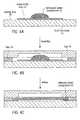
- FIG. 2Aillustrates a prior art glass cap with a cavity.
- FIG. 2Billustrates a glass cap including an active getter, according to an embodiment of the invention.
- FIG. 2Cillustrates a glass cap including an active getter and an adjacent binder layer, representing an embodiment of the invention.
- FIG. 3Aillustrates a microelectronics device assembly including the cap of FIG. 2C , representing an embodiment of the invention.
- FIG. 3Billustrates a microelectronics device assembly after the inert layer has been removed from the active getter, representing an embodiment of the invention.
- FIG. 4Aillustrates the placement of a reflowable getter composition onto a microelectronic device prior to encapsulation, representing an embodiment of the invention.
- FIG. 4Billustrates a microelectronic device assembly with the getter composition after encapsulation, and sealing.
- FIG. 4Cillustrates a microelectronic device assembly after reflow of the getter composition so that the getter composition covers the entire active area of the microelectronic device.
- Coupledis defined as connected, although not necessarily directly, and not necessarily mechanically.
- substantiallyis defined as approximately (e.g., preferably within 10% of, more preferably within 1% of, most preferably within 0.1% of).
- Some embodiments according to a first aspect of the inventionprovide a method for protecting circuit device materials. Examples of these embodiments are depicted in FIGS. 1A , 1 B, 3 A, 3 B, 4 A, 4 B, and 4 C.
- the methodcomprises mixing a reactive material 12 A with a comparatively inert material 12 B to form a getter 12 ; placing the getter in the device 10 ; applying energy to the getter; and responsive to applying the energy, distributing the getter inside the device.
- the comparative inertnessis relative to the reactive material.
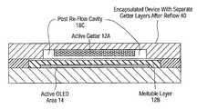
- a reflowed getter composition 22covers an active OLED area 14 .
- the reflowed getter compositioncan also be used to cover active areas of other optoelectronic devices including light detector arrays or solar cell arrays.
- the inert material 12 Bcan comprise a binder.
- the placingcan be accomplished by automated means.
- the method for protecting circuit device materialsfurther comprises sealing the device.
- the devicecan comprise an optoelectronic device.
- the optoelectronic devicecan include a substrate 16 and an active OLED area 14 .
- placing the getter 12can include placing the getter on a surface of a cap 18 , sealing the device includes joining the cap to the substrate.
- Distributing the getter 12can include transferring at least a portion of the getter to cover the active OLED area 14 . Transferring at least a portion of the getter 12 to cover the active OLED area 14 can include heating the getter to a temperature in the range of 75 to 300 degrees Celsius, and can provide an encapsulated device after reflow of the getter 20 as shown in FIG. 1B .
- the portion of the getter 12 transferred to cover the active OLED area 14can be greater than approximately eighty percent.
- the active OLED area 14can include a central portion and a periphery. Distributing the getter 12 can include covering at least 50% of the periphery of the active OLED area 14 . The distributing can occur after final assembly of an encapsulated device before reflow of the getter 10 as shown in FIG. 1A .
- Some embodiments according to a second aspect of the inventionprovide a method for protecting circuit device materials. Examples of these embodiments are depicted in FIGS. 3A and 3B .
- the methodcomprises placing a reactive material 12 A on an interior surface of the device 10 ; placing a meltable material 12 B upon the reactive material to substantially cover the reactive material; and in response to an application of energy to the meltable material, removing at least a portion of the meltable material, the removing exposing at least a portion of the reactive material.
- the circuit devicecan comprise an optoelectronic device including an active OLED area 14 .
- the removing stepcan include heating the meltable material 12 B to a temperature in the range of 75 to 300 degrees Celsius.
- the removing stepcan further comprise covering substantially all of the active OLED area 14 with the meltable material 12 B.
- the methodcan further comprise sealing the device.
- the methods for protecting circuit devicesprovide more flexible handling of the getter 12 during fabrication of optoelectronic devices.
- the comparative size and shape of a getter 12 with respect to the size and shape of the encapsulating cavityhas an impact on the performance of the getter. and thus potentially the degradation of the optoelectronic device.
- the permeation of water vapor and other potentially harmful gaseous species through the seal 19may cause some non-uniform degradation of the display at the periphery of the device if the getter 12 is placed only at the center of the device.
- the present inventionenables modification of the shape and activity of the getter 12 after sealing of the device.
- the optoelectronic devicecomprises a substrate 16 ; an active device area placed on the substrate; and a getter 12 .
- the getter 12includes a first material 12 B and a reactive material 12 A.
- the first material 12 Bcan be adapted to respond to energy input by at least one of: melting, phase change, or morphological change.
- An example of the active device areais shown in FIG. 3B as an active OLED area 14 .
- the optoelectronic devicecan further comprise a seal 19 joining the substrate 16 to a cap 18 .
- the at least one of: melting, phase change, and morphological changecan result in reflowing of the first material 12 B.
- the getter 12Prior to the reflowing, the getter 12 can be disposed on a recessed surface of the cap 18 . After the reflowing, the getter 12 can be disposed to cover a substantial portion of the active OLED area 14 .
- the first material 12 Bcan comprise at least one of paraffin wax, low-density polyethylene, or Elvax resin.
- the first material 12 Bcan comprise a binder, and the reactive material 12 A can be substantially dispersed within the binder.
- Some embodiments according to a fourth aspect of the inventionprovide a cap 18 for enclosing an optoelectronic device. Examples of these embodiments are depicted in FIG. 2C .
- the cap 18comprises a reactive material 12 A disposed on a cap surface; and an inert material 12 B placed to cover more than approximately fifty percent of the reactive material.
- the inert material 12 Bcan be adapted to flow in response to application of energy to the inert material.
- the cap 18can include an interior surface having a recessed portion.
- the inert material 12 Bcan cover at least some of the recessed portion. In response to the application of energy, the inert material 12 B can melt.
- the inert material 12 Bcan cover less than the entire recessed portion thereby leaving a cavity between the inert material and at least one sidewall 18 D of the recessed portion.
- the reflowable getter composition 12can be formed as a reactive material 12 A dispersed within an inert binder 12 B.
- the getter compositioncan comprise: a reactive material 12 A disposed in an encapsulated device 10 , and an inert material 12 B disposed in the encapsulated device.
- the reactive material 12 Ais more reactive than at least one device material to desorbed matter and matter from a space within the device.
- the desorbed mattercan be desorbed from at least one of: a substrate, a film disposed upon the substrate, and an encapsulation surface.
- the inert material 12 Bcan be adapted to respond to energy input by at least one of: melting, phase change, or morphological change.
- the reactive material 12 Acan comprise an activated powder containing at least one of activated alumina, silica, zeolite, barium oxide, calcium oxide, calcium, and barium.
- the inert material 12 Bcan comprise at least one of paraffin wax, low-density polyethylene, or Elvax® resin.
- the inert material 12 Bcan comprise a binder, and the reactive material 12 A, e.g. activated powder can be mixed with the binder so that the reactive material is substantially dispersed in the binder.
- the inert material 12 Bresponds to energy input by melting. Upon removal of the energy, the inert material 12 B solidifies. In some of these embodiments, each device material is adapted to provide enhanced performance of an optoelectronic device.
- a getter 12comprised of an reactive material 12 A (activated powder) mixed with a inert material 12 B (binder) is selected to provide an equilibrium minimum humidity level lower than a humidity level to which the OLED device is sensitive when sealingly enclosed by an enclosure containing the getter;
- the activated powdercan have a particle size range of about 0.1 to about 200 micrometers.
- the bindercan be chosen for dispersing the selected activated powder therein.
- the inert material 12 B (binder)can be chosen from various classes of materials so that the binder can have a low moisture absorption rate; e.g., if the binder is selected from non polar hydrocarbons such as waxes, paraffins, polyolefins. Alternatively, the inert material 12 B (binder) can have a higher moisture absorption rate if selected from more polar materials such as low molecular weight acrylates, polyurethanes, polyamides. During reflow of the inert material 12 B, the moisture absorption rate of the binder may change.
- the inert material 12 Bcan be selected so that a blend can be formed of the reactive material 12 A (activated powder) and the inert material 12 B (e.g., wax) in a preferred weight fraction of the activated powder in the blend in a range of approximately 10% to 90%.
- a measured amount of the getter 12 blendcan then be applied on a portion of the upper interior surface of a glass cap 18 by dispensing a measured amount of the getter 12 blend above the blend's melting point with a heated syringe dispensing system until the dispensed blend has spread along the interior surface to form a reflowable getter layer 12 .
- the dispensed blendcan have any shape (such as a droplet), so that there is no need to initially dispense the blend uniformly onto the surface of the enclosure.
- the getter 12 compositioncan be shaped as a thin pellet whose shape and dimension are such that the pellet can fit in the cavity of the device to be protected, and this pellet can be placed inside the device cavity.
- the pelletcan be placed directly on top of the active OLED area 14 , or in the cap 18 . The placement can be accomplished either manually or through use of automatic pick-and-place equipment.
- the preparation of the getter 12 according to other embodiments of the invention, as shown in FIGS. 2C , 3 A, and 3 B,is as follows:
- a reactive material 12 Ae.g., an active getter, is selected to provide an equilibrium minimum humidity level lower than a humidity level to which the device is sensitive when sealingly enclosed by an enclosure containing the active getter.
- the reactive material 12 Acan be a reactive metal such as barium.
- Reactive material 12 Acan be deposited onto the cap 18 by physical vapor deposition techniques, e.g., thermal evaporation or sputter deposition; or by chemical vapor deposition techniques.
- reactive material 12 Acan be a finely-divided powder of a reactive metal or an alkaline metal oxide and has a preferred particle size range of about 0.1 to about 200 micrometers. In some embodiments the particle size range is from 0.3 to 50 micrometers.
- a meltable inert material 12 Be.g., a molten wax, can be chosen for coating the reactive material 12 A before reflow, and for coating the active OLED area 14 after reflow.
- a measured amount of the reactive material 12 Acan be applied on a portion of the recessed interior surface of the cap 18 , for example by evaporation of a reactive metal, until the reactive material 12 A has formed a layer along the desired area of the recessed portion of the interior surface of the cap.
- the capPrior to placement of the reactive material 12 A on the cap 18 , the cap has a pre-getter placement cavity 18 A.
- the portion of the recessed interior surface covered by the reactive material 12 Ais in a range of 25% to 90%.
- the portion of the inner surface covered by the reactive material 12 Acan be in the range of 10% to 99%.
- a volume of space underneath the cap after application of reactive material 12 Ais bounded by a cap sidewall 18 D and the lateral extent of the inert material 12 B, and is referred to as the pre-reflow cavity 18 B.
- inert material 12 Bhas transferred to the active OLED area 14 , the remaining reactive material 12 A extends towards the sidewall 18 D, and the volume of space underneath cap is referred to as the post re-flow cavity 18 C.
- the reactive material 12 A layerhas a thickness in the range of about 0.1 micron to 10 microns.
- meltable inert material 12 BUnder controlled conditions (e.g., low moisture atmosphere) a measured amount of inert material 12 B, e.g., meltable material, is then placed upon the reactive material 12 A (active getter).
- the meltable inert material 12 Bcovers substantially all of the reactive material 12 A, and in some embodiments also extends to cover a portion of the recessed portion of the interior surface of the cap 18 .
- the meltable inert material 12 Bdoes not cover the entire length of the recessed portion of the interior surface.
- the active getter layerbecomes much less susceptible to deactivation by ambient conditions (i.e., the active getter layer is less susceptible to loss of gettering capacity due to reactions with ambient gases), and thus the caps can be easier to handle in a mass production process.
- the reactive material 12 Acan be uncovered by melting and displacing the meltable inert material 12 B as needed to regain its gettering function.
- a reflowable getter composition 12can be made (under controlled conditions, e.g, using a glove box where the oxygen and moisture concentration can be reduced to a very low level when mixing a reactive material 12 A (e.g., activated powder) with an inert material 12 B (e.g., molten wax).
- the activated powder 12 Acan be activated silica gel, alumina, activated zeolite powder, barium oxide (BaO) or other alkaline earth metal oxides, or barium (Ba) powder or other alkaline metals or alkaline earth metals.
- the inert material 12 Bcan be natural or synthetic waxes, paraffin waxes, microcrystalline waxes, polyolefin resin waxes such as polyethylene, polypropylene, polybutene, polyethylene oxide, polypropylene oxide and their copolymers such as Elvax® resin from DuPont; ester waxes, polyurethane waxes, silicone resin waxes.
- the getter composition 12can be shaped as a thin tablet and placed into the enclosure of the device to be protected, such as encapsulated device before reflow 10 .
- the sealed encapsulated device before reflow 10includes: reflowable getter composition 12 , an active OLED area 14 , an OLED substrate 16 , a glass cap with a cavity 18 , and at least one epoxy seal 19 .
- the reflowable getter composition 12can melt and distribute itself evenly inside the device to form an encapsulated device after getter reflow 20 , as shown in FIG. 1B .
- the getter materialmay be uniformly distributed on the entire inner surface of the device. It has been observed that the shape of the getter material is important to protect such a display from degradation. If the getter material is placed in the center of the display, some degradation is observed on the periphery of the active area of the display.
- the getter compositioncan be melted so that it distributes itself evenly inside the cavity, the periphery of the active layers of the display will be better protected since any moisture of oxygen permeating inside the device through the epoxy seal on the periphery will react first with the getter material.
- an reactive material 12 Acan be deposited (by evaporation or other means) onto a glass cap 18 .
- the active gettercan be a reactive metal, such as barium.
- the reactive material 12 Acan then be protected with a thin film of a metlable inert layer 12 B, such as paraffin wax, so that the cap 18 can be manufactured and handled easily.
- the cap 18can then be used to encapsulate a device, using an epoxy seal 19 or other conventional means.
- the assemblyis then subjected to thermal, or other, energy so that the metlable inert layer 12 B melts, exposing the reactive material 12 A to the atmosphere of the device on the one hand, and further protecting the active parts of the device by covering the inside of the device with a thin layer of wax, as shown in FIG. 3B .
- the reflowable getter 12can be advantageously used in the production of OLEDs.
- An appropriate amount of the getter 12 composition as described in Example 1can be dispensed as a hot liquid onto a glass or a metal cap 18 with a heated syringe and cooled down to room temperature so that the liquid getter composition solidifies.
- the substrate 16 having the active OLED area 14can then be sealed with this cap 18 using a sealant such as a UV-curable epoxy adhesive. Once cured, the OLED assembly can be heated above the melting point of the inert material 12 B (wax/binder), thus causing the reflowable getter composition to flow inside the entire inner cavity, and evenly distributing the getter particles inside the device cavity.
- the inert material 12 Be.g., wax or binder
- the inert material 12 Bcan wet and spread itself inside the device cavity because of the inert material's low surface tension, especially where the getter 12 , in its molten state, is reasonably fluid and does not behave as a thixotropic liquid.
- the inert material 12 Be.g., wax
- the inert material 12 Bcan provide additional protection to the active OLED area 14 .
- the reflowable getter 12can be placed (as a liquid droplet or as a solid tablet) directly on top of the active OLED area 14 , as shown in FIG. 4A .
- the cap 18can then be placed onto the OLED device with the appropriate sealant such as a UV-curable epoxy.
- the sealing surfaces in contact with the sealing materialare preferably very clean and not contaminated with materials used in the manufacturing process of the active OLED area, such as photoresists, solvents, or organic light emitting materials.
- the sealing areais cleaned by an ablation process just before encapsulation.
- the reflowable getter 12can be heated above its melting point, causing the getter to flow inside the cavity up to the edge of the sealing area. Such edge coverage is otherwise difficult to achieve without the risk of contaminating the sealing area.
- the effectiveness of a getter 12 in an OLED devicecan be evaluated by measuring the dimensions of the light emitting areas (pixels) after exposure to a testing environment, with respect to the initial light emitting areas.
- the shrinkage of the light emitting areasis more severe at the periphery of the OLED display, close to the sealing area, especially when the getter is placed at the center of the cap.
- Uniformly reflowing the getter 12 inside the OLED cavityprovides more uniform shrinkage of the light emitting areas.
- the inert binder material 12 Bprovides additional protection to the active OLED area, in the case where the inert binder material has been reflowed over the active OLED area 14 , as shown in FIGS. 3B and 4C .
Landscapes
- Engineering & Computer Science (AREA)
- Microelectronics & Electronic Packaging (AREA)
- Physics & Mathematics (AREA)
- Manufacturing & Machinery (AREA)
- Optics & Photonics (AREA)
- Condensed Matter Physics & Semiconductors (AREA)
- General Physics & Mathematics (AREA)
- Computer Hardware Design (AREA)
- Power Engineering (AREA)
- Electroluminescent Light Sources (AREA)
Abstract
Description
Claims (7)
Priority Applications (3)
| Application Number | Priority Date | Filing Date | Title |
|---|---|---|---|
| US13/193,033US8310154B2 (en) | 2003-03-24 | 2011-07-28 | Devices including, methods using, and compositions of reflowable getters |
| US13/633,332US8905808B2 (en) | 2003-03-24 | 2012-10-02 | Devices including, methods using, and compositions of reflowable getters |
| US14/561,754US9318724B2 (en) | 2003-03-24 | 2014-12-05 | Devices including, methods using, and compositions of reflowable getters |
Applications Claiming Priority (4)
| Application Number | Priority Date | Filing Date | Title |
|---|---|---|---|
| US45740403P | 2003-03-24 | 2003-03-24 | |
| US10/606,726US20040189195A1 (en) | 2003-03-24 | 2003-06-26 | Devices including, methods using, and compositions of reflowable getters |
| US11/845,719US8013526B2 (en) | 2003-03-24 | 2007-08-27 | Devices including, methods using, and compositions of reflowable getters |
| US13/193,033US8310154B2 (en) | 2003-03-24 | 2011-07-28 | Devices including, methods using, and compositions of reflowable getters |
Related Parent Applications (1)
| Application Number | Title | Priority Date | Filing Date |
|---|---|---|---|
| US11/845,719ContinuationUS8013526B2 (en) | 2003-03-24 | 2007-08-27 | Devices including, methods using, and compositions of reflowable getters |
Related Child Applications (1)
| Application Number | Title | Priority Date | Filing Date |
|---|---|---|---|
| US13/633,332ContinuationUS8905808B2 (en) | 2003-03-24 | 2012-10-02 | Devices including, methods using, and compositions of reflowable getters |
Publications (2)
| Publication Number | Publication Date |
|---|---|
| US20110285004A1 US20110285004A1 (en) | 2011-11-24 |
| US8310154B2true US8310154B2 (en) | 2012-11-13 |
Family
ID=32994842
Family Applications (6)
| Application Number | Title | Priority Date | Filing Date |
|---|---|---|---|
| US10/606,726AbandonedUS20040189195A1 (en) | 2003-03-24 | 2003-06-26 | Devices including, methods using, and compositions of reflowable getters |
| US11/845,719Expired - Fee RelatedUS8013526B2 (en) | 2003-03-24 | 2007-08-27 | Devices including, methods using, and compositions of reflowable getters |
| US13/193,033Expired - Fee RelatedUS8310154B2 (en) | 2003-03-24 | 2011-07-28 | Devices including, methods using, and compositions of reflowable getters |
| US13/197,299Expired - Fee RelatedUS8310155B2 (en) | 2003-03-24 | 2011-08-03 | Devices including, methods using, and compositions of reflowable getters |
| US13/633,332Expired - LifetimeUS8905808B2 (en) | 2003-03-24 | 2012-10-02 | Devices including, methods using, and compositions of reflowable getters |
| US14/561,754Expired - Fee RelatedUS9318724B2 (en) | 2003-03-24 | 2014-12-05 | Devices including, methods using, and compositions of reflowable getters |
Family Applications Before (2)
| Application Number | Title | Priority Date | Filing Date |
|---|---|---|---|
| US10/606,726AbandonedUS20040189195A1 (en) | 2003-03-24 | 2003-06-26 | Devices including, methods using, and compositions of reflowable getters |
| US11/845,719Expired - Fee RelatedUS8013526B2 (en) | 2003-03-24 | 2007-08-27 | Devices including, methods using, and compositions of reflowable getters |
Family Applications After (3)
| Application Number | Title | Priority Date | Filing Date |
|---|---|---|---|
| US13/197,299Expired - Fee RelatedUS8310155B2 (en) | 2003-03-24 | 2011-08-03 | Devices including, methods using, and compositions of reflowable getters |
| US13/633,332Expired - LifetimeUS8905808B2 (en) | 2003-03-24 | 2012-10-02 | Devices including, methods using, and compositions of reflowable getters |
| US14/561,754Expired - Fee RelatedUS9318724B2 (en) | 2003-03-24 | 2014-12-05 | Devices including, methods using, and compositions of reflowable getters |
Country Status (1)
| Country | Link |
|---|---|
| US (6) | US20040189195A1 (en) |
Cited By (1)
| Publication number | Priority date | Publication date | Assignee | Title |
|---|---|---|---|---|
| US11889713B2 (en)* | 2018-10-02 | 2024-01-30 | Sony Semiconductor Solutions Corporation | Display device and electronic apparatus including seal part outside recess |
Families Citing this family (38)
| Publication number | Priority date | Publication date | Assignee | Title |
|---|---|---|---|---|
| US7508132B2 (en)* | 2003-10-20 | 2009-03-24 | Hewlett-Packard Development Company, L.P. | Device having a getter structure and a photomask |
| JP2005190703A (en)* | 2003-12-24 | 2005-07-14 | Tohoku Pioneer Corp | Organic EL panel and manufacturing method thereof |
| US7164520B2 (en)* | 2004-05-12 | 2007-01-16 | Idc, Llc | Packaging for an interferometric modulator |
| US7710629B2 (en)* | 2004-09-27 | 2010-05-04 | Qualcomm Mems Technologies, Inc. | System and method for display device with reinforcing substance |
| US20060076632A1 (en)* | 2004-09-27 | 2006-04-13 | Lauren Palmateer | System and method for display device with activated desiccant |
| FR2883099B1 (en) | 2005-03-14 | 2007-04-13 | Commissariat Energie Atomique | PROTECTION OF A THIN LAYER GETTER |
| US20080087323A1 (en)* | 2005-05-09 | 2008-04-17 | Kenji Araki | Concentrator Solar Photovoltaic Power Generating Apparatus |
| WO2007120887A2 (en) | 2006-04-13 | 2007-10-25 | Qualcomm Mems Technologies, Inc | Packaging a mems device using a frame |
| WO2007123039A1 (en)* | 2006-04-18 | 2007-11-01 | Komatsu Seiren Co., Ltd. | Hot-melt type member and organic el display panel |
| WO2007136706A1 (en)* | 2006-05-17 | 2007-11-29 | Qualcomm Mems Technologies Inc. | Desiccant in a mems device |
| KR100826011B1 (en)* | 2006-10-24 | 2008-04-29 | 엘지디스플레이 주식회사 | Display elements |
| US7816164B2 (en)* | 2006-12-01 | 2010-10-19 | Qualcomm Mems Technologies, Inc. | MEMS processing |
| EP2064148A1 (en)* | 2007-09-28 | 2009-06-03 | Qualcomm Mems Technologies, Inc | Optimization of desiccant usage in a mems package |
| ITMI20071903A1 (en)* | 2007-10-04 | 2009-04-05 | Getters Spa | METHOD FOR THE PRODUCTION OF SOLAR PANELS THROUGH THE USE OF A POLYMER TRISTRATE INCLUDING A COMPOSITE GETTER SYSTEM |
| US8410690B2 (en)* | 2009-02-13 | 2013-04-02 | Qualcomm Mems Technologies, Inc. | Display device with desiccant |
| KR101086880B1 (en)* | 2009-05-28 | 2011-11-24 | 네오뷰코오롱 주식회사 | Method for manufacturing organic light emitting display device having getter layer |
| KR20130008100A (en)* | 2011-06-22 | 2013-01-22 | 삼성디스플레이 주식회사 | Organic light emitting diode lighting apparatus |
| FR2981198B1 (en)* | 2011-10-11 | 2014-04-04 | Commissariat Energie Atomique | ELECTRONIC DEVICE ENCAPSULATION STRUCTURE AND METHOD FOR PRODUCING SUCH STRUCTURE |
| FR2982073B1 (en) | 2011-10-28 | 2014-10-10 | Commissariat Energie Atomique | HERMETIC ENCAPSULATION STRUCTURE OF A DEVICE AND AN ELECTRONIC COMPONENT |
| ITMI20111987A1 (en) | 2011-11-03 | 2013-05-04 | Getters Spa | IMPROVED COMPOSITE GETTERS |
| US20130154471A1 (en)* | 2011-12-15 | 2013-06-20 | General Electric Company | Oled devices |
| DE102012214411B4 (en)* | 2012-08-14 | 2022-05-25 | Osram Oled Gmbh | DEVICE AND METHOD FOR MAKING HERMETICALLY TIGHT CAVITIES |
| TWI518896B (en)* | 2013-09-05 | 2016-01-21 | 元太科技工業股份有限公司 | Organic light-emitting display device |
| CN103490016B (en)* | 2013-09-24 | 2016-10-05 | 京东方科技集团股份有限公司 | A kind of encapsulating structure of OLED |
| CN103762296B (en)* | 2014-01-08 | 2017-03-29 | 广东工业大学 | A kind of package structure for LED |
| EP3034548A1 (en)* | 2014-12-18 | 2016-06-22 | Nederlandse Organisatie voor toegepast- natuurwetenschappelijk onderzoek TNO | Barrier film laminate comprising submicron getter particles and electronic device comprising such a laminate |
| CN104934550A (en)* | 2015-05-07 | 2015-09-23 | 京东方科技集团股份有限公司 | OLED device packaging structure, packaging method and electronic device |
| EP3252444B1 (en) | 2016-06-01 | 2023-12-20 | Sonion Nederland B.V. | Vibration or acceleration sensor applying squeeze film damping |
| WO2018093653A1 (en)* | 2016-11-15 | 2018-05-24 | Corning Incorporated | Apparatus and method for processing the apparatus |
| EP3702322A1 (en)* | 2016-12-30 | 2020-09-02 | Sonion Nederland B.V. | Micro-electromechanical transducer |
| US10942257B2 (en) | 2016-12-31 | 2021-03-09 | Innovusion Ireland Limited | 2D scanning high precision LiDAR using combination of rotating concave mirror and beam steering devices |
| US11579300B1 (en) | 2018-08-21 | 2023-02-14 | Innovusion, Inc. | Dual lens receive path for LiDAR system |
| US11614526B1 (en) | 2018-08-24 | 2023-03-28 | Innovusion, Inc. | Virtual windows for LIDAR safety systems and methods |
| CN109728192B (en)* | 2018-11-30 | 2021-01-26 | 云谷(固安)科技有限公司 | Packaging structure and display device |
| US12204033B2 (en) | 2022-03-25 | 2025-01-21 | Seyond, Inc. | Multimodal detection with integrated sensors |
| US20230324308A1 (en)* | 2022-04-08 | 2023-10-12 | Advanced Semiconductor Engineering, Inc. | Electronic package |
| CN116387654B (en)* | 2023-06-05 | 2023-09-26 | 厦门海辰储能科技股份有限公司 | Energy storage devices and electrical equipment |
| CN116387714B (en)* | 2023-06-05 | 2023-08-25 | 厦门海辰储能科技股份有限公司 | End cover assembly, energy storage device and electrical equipment |
Citations (25)
| Publication number | Priority date | Publication date | Assignee | Title |
|---|---|---|---|---|
| US4671889A (en) | 1982-08-10 | 1987-06-09 | Horst Schreiner | Molded getter bodies and method of producing the same |
| US5244707A (en) | 1992-01-10 | 1993-09-14 | Shores A Andrew | Enclosure for electronic devices |
| US5304419A (en) | 1990-07-06 | 1994-04-19 | Alpha Fry Ltd | Moisture and particle getter for enclosures |
| US5840142A (en) | 1996-11-22 | 1998-11-24 | Stevenson; Michael J. | Decoration and printing on polyolefin surfaces |
| US6059860A (en) | 1996-06-21 | 2000-05-09 | 3M Innovative Properties Company | Sorptive articles |
| US6077404A (en) | 1998-02-17 | 2000-06-20 | Applied Material, Inc. | Reflow chamber and process |
| US6112888A (en) | 1996-06-28 | 2000-09-05 | W. R. Grace & Co.-Conn. | Non-reclosable packages containing desiccant matrix |
| US6124006A (en) | 1995-04-19 | 2000-09-26 | Capitol Specialty Plastics, Inc. | Modified polymers having controlled transmission rates |
| US6180708B1 (en) | 1996-06-28 | 2001-01-30 | W. R. Grace & Co.-Conn. | Thermoplastic adsorbent compositions containing wax and insulating glass units containing such compositions |
| US6226890B1 (en) | 2000-04-07 | 2001-05-08 | Eastman Kodak Company | Desiccation of moisture-sensitive electronic devices |
| US20010033946A1 (en) | 2000-03-23 | 2001-10-25 | Hiroaki Mashiko | Fixing member, electroluminescent device using the member and backing substrate for the device |
| US20020155320A1 (en)* | 2001-04-20 | 2002-10-24 | Lg.Philips Lcd Co., Ltd. | Organic electroluminescent device |
| US6470594B1 (en) | 2001-09-21 | 2002-10-29 | Eastman Kodak Company | Highly moisture-sensitive electronic device element and method for fabrication utilizing vent holes or gaps |
| US20020181866A1 (en) | 2001-04-25 | 2002-12-05 | Crook Russell A. | Low cost adhesive bonding of getter |
| US6562452B2 (en) | 1998-08-14 | 2003-05-13 | Truseal Technologies, Inc. | Dispensable non-adhesive desiccated matrix system for insulating glass units |
| US6737176B1 (en) | 1999-07-15 | 2004-05-18 | Nec Corporation | Organic electroluminescent device and method for fabricating same |
| US20040099862A1 (en)* | 2002-11-27 | 2004-05-27 | Harumi Suzuki | Organic EL device and repair method thereof |
| US20040108811A1 (en) | 2002-09-11 | 2004-06-10 | Hagen Klausmann | OLED Devices with Improved Encapsulation |
| US6835950B2 (en) | 2002-04-12 | 2004-12-28 | Universal Display Corporation | Organic electronic devices with pressure sensitive adhesive layer |
| US6843936B1 (en) | 1998-10-22 | 2005-01-18 | Texas Instruments Incorporated | Getter for enhanced micromechanical device performance |
| US6936131B2 (en) | 2002-01-31 | 2005-08-30 | 3M Innovative Properties Company | Encapsulation of organic electronic devices using adsorbent loaded adhesives |
| US6967640B2 (en) | 2001-07-27 | 2005-11-22 | E Ink Corporation | Microencapsulated electrophoretic display with integrated driver |
| US7309747B2 (en) | 2002-02-21 | 2007-12-18 | Idemitsu Kosan Co., Ltd. | Highly flowable 1-butene polymer and process for producing the same |
| US20090174304A1 (en) | 2006-04-18 | 2009-07-09 | Komatsu Seiren Co., Ltd. | Hot-melt type member and organic el display panel |
| US7589465B2 (en) | 2004-08-12 | 2009-09-15 | Osram Opto Semiconductors Gmbh | Getter material |
Family Cites Families (10)
| Publication number | Priority date | Publication date | Assignee | Title |
|---|---|---|---|---|
| US4950193A (en)* | 1988-10-27 | 1990-08-21 | Samsung Electron Devices Co., Ltd. | Manufacturing method for fluorescent indicator panel |
| KR930008616B1 (en)* | 1990-06-25 | 1993-09-10 | 삼성전관 주식회사 | Manufacturing Method of Color Brown Tube |
| US5308533A (en)* | 1991-11-29 | 1994-05-03 | The United States Of America As Represented By The Secretary Of The Air Force | Aerogel mesh getter |
| RU2118231C1 (en)* | 1997-03-28 | 1998-08-27 | Товарищество с ограниченной ответственностью "ТЕХНОВАК+" | Method of preparing non-evaporant getter and getter prepared by this method |
| JP4434411B2 (en)* | 2000-02-16 | 2010-03-17 | 出光興産株式会社 | Active drive type organic EL light emitting device and manufacturing method thereof |
| US6407408B1 (en)* | 2001-03-12 | 2002-06-18 | Universal Display Corporation | Method for patterning devices |
| US6900470B2 (en)* | 2001-04-20 | 2005-05-31 | Kabushiki Kaisha Toshiba | Display device and method of manufacturing the same |
| US6808828B2 (en)* | 2001-08-23 | 2004-10-26 | Tohoku Pioneer Corporation | Organic electroluminescent display panel |
| JP3922374B2 (en)* | 2002-09-25 | 2007-05-30 | セイコーエプソン株式会社 | Electro-optical device, matrix substrate, and electronic apparatus |
| US7789949B2 (en)* | 2005-11-23 | 2010-09-07 | Integrated Sensing Systems, Inc. | Getter device |
- 2003
- 2003-06-26USUS10/606,726patent/US20040189195A1/ennot_activeAbandoned
- 2007
- 2007-08-27USUS11/845,719patent/US8013526B2/ennot_activeExpired - Fee Related
- 2011
- 2011-07-28USUS13/193,033patent/US8310154B2/ennot_activeExpired - Fee Related
- 2011-08-03USUS13/197,299patent/US8310155B2/ennot_activeExpired - Fee Related
- 2012
- 2012-10-02USUS13/633,332patent/US8905808B2/ennot_activeExpired - Lifetime
- 2014
- 2014-12-05USUS14/561,754patent/US9318724B2/ennot_activeExpired - Fee Related
Patent Citations (29)
| Publication number | Priority date | Publication date | Assignee | Title |
|---|---|---|---|---|
| US4671889A (en) | 1982-08-10 | 1987-06-09 | Horst Schreiner | Molded getter bodies and method of producing the same |
| US5304419A (en) | 1990-07-06 | 1994-04-19 | Alpha Fry Ltd | Moisture and particle getter for enclosures |
| US5591379A (en) | 1990-07-06 | 1997-01-07 | Alpha Fry Limited | Moisture getting composition for hermetic microelectronic devices |
| US5244707A (en) | 1992-01-10 | 1993-09-14 | Shores A Andrew | Enclosure for electronic devices |
| US5401536A (en) | 1992-01-10 | 1995-03-28 | Shores; A. Andrew | Method of providing moisture-free enclosure for electronic device |
| US6124006A (en) | 1995-04-19 | 2000-09-26 | Capitol Specialty Plastics, Inc. | Modified polymers having controlled transmission rates |
| US6059860A (en) | 1996-06-21 | 2000-05-09 | 3M Innovative Properties Company | Sorptive articles |
| US6777481B2 (en) | 1996-06-28 | 2004-08-17 | W. R. Grace & Co.-Conn. | Thermoplastic adsorbent compositions containing wax and insulating glass units containing such compositions |
| US6112888A (en) | 1996-06-28 | 2000-09-05 | W. R. Grace & Co.-Conn. | Non-reclosable packages containing desiccant matrix |
| US6180708B1 (en) | 1996-06-28 | 2001-01-30 | W. R. Grace & Co.-Conn. | Thermoplastic adsorbent compositions containing wax and insulating glass units containing such compositions |
| US5840142A (en) | 1996-11-22 | 1998-11-24 | Stevenson; Michael J. | Decoration and printing on polyolefin surfaces |
| US6077404A (en) | 1998-02-17 | 2000-06-20 | Applied Material, Inc. | Reflow chamber and process |
| US6299689B1 (en) | 1998-02-17 | 2001-10-09 | Applied Materials, Inc. | Reflow chamber and process |
| US6562452B2 (en) | 1998-08-14 | 2003-05-13 | Truseal Technologies, Inc. | Dispensable non-adhesive desiccated matrix system for insulating glass units |
| US6843936B1 (en) | 1998-10-22 | 2005-01-18 | Texas Instruments Incorporated | Getter for enhanced micromechanical device performance |
| US6737176B1 (en) | 1999-07-15 | 2004-05-18 | Nec Corporation | Organic electroluminescent device and method for fabricating same |
| US20010033946A1 (en) | 2000-03-23 | 2001-10-25 | Hiroaki Mashiko | Fixing member, electroluminescent device using the member and backing substrate for the device |
| US6226890B1 (en) | 2000-04-07 | 2001-05-08 | Eastman Kodak Company | Desiccation of moisture-sensitive electronic devices |
| US20020155320A1 (en)* | 2001-04-20 | 2002-10-24 | Lg.Philips Lcd Co., Ltd. | Organic electroluminescent device |
| US20020181866A1 (en) | 2001-04-25 | 2002-12-05 | Crook Russell A. | Low cost adhesive bonding of getter |
| US6967640B2 (en) | 2001-07-27 | 2005-11-22 | E Ink Corporation | Microencapsulated electrophoretic display with integrated driver |
| US6470594B1 (en) | 2001-09-21 | 2002-10-29 | Eastman Kodak Company | Highly moisture-sensitive electronic device element and method for fabrication utilizing vent holes or gaps |
| US6936131B2 (en) | 2002-01-31 | 2005-08-30 | 3M Innovative Properties Company | Encapsulation of organic electronic devices using adsorbent loaded adhesives |
| US7309747B2 (en) | 2002-02-21 | 2007-12-18 | Idemitsu Kosan Co., Ltd. | Highly flowable 1-butene polymer and process for producing the same |
| US6835950B2 (en) | 2002-04-12 | 2004-12-28 | Universal Display Corporation | Organic electronic devices with pressure sensitive adhesive layer |
| US20040108811A1 (en) | 2002-09-11 | 2004-06-10 | Hagen Klausmann | OLED Devices with Improved Encapsulation |
| US20040099862A1 (en)* | 2002-11-27 | 2004-05-27 | Harumi Suzuki | Organic EL device and repair method thereof |
| US7589465B2 (en) | 2004-08-12 | 2009-09-15 | Osram Opto Semiconductors Gmbh | Getter material |
| US20090174304A1 (en) | 2006-04-18 | 2009-07-09 | Komatsu Seiren Co., Ltd. | Hot-melt type member and organic el display panel |
Cited By (1)
| Publication number | Priority date | Publication date | Assignee | Title |
|---|---|---|---|---|
| US11889713B2 (en)* | 2018-10-02 | 2024-01-30 | Sony Semiconductor Solutions Corporation | Display device and electronic apparatus including seal part outside recess |
Also Published As
| Publication number | Publication date |
|---|---|
| US8013526B2 (en) | 2011-09-06 |
| US8905808B2 (en) | 2014-12-09 |
| US20150139864A1 (en) | 2015-05-21 |
| US20130089971A1 (en) | 2013-04-11 |
| US20110284916A1 (en) | 2011-11-24 |
| US20080042561A1 (en) | 2008-02-21 |
| US8310155B2 (en) | 2012-11-13 |
| US20110285004A1 (en) | 2011-11-24 |
| US9318724B2 (en) | 2016-04-19 |
| US20040189195A1 (en) | 2004-09-30 |
Similar Documents
| Publication | Publication Date | Title |
|---|---|---|
| US9318724B2 (en) | Devices including, methods using, and compositions of reflowable getters | |
| US6740145B2 (en) | Desiccants and desiccant packages for highly moisture-sensitive electronic devices | |
| TW560033B (en) | Highly moisture-sensitive electronic device element and method for fabrication | |
| US6226890B1 (en) | Desiccation of moisture-sensitive electronic devices | |
| TW560025B (en) | Sealing structure for highly moisture sensitive electronic device element and method for fabrication | |
| US6470594B1 (en) | Highly moisture-sensitive electronic device element and method for fabrication utilizing vent holes or gaps | |
| US4426769A (en) | Moisture getter for integrated circuit packages | |
| CN1894790B (en) | Method for adhering getter material to a surface for use in electronic devices | |
| EP3019441A1 (en) | Wafer level package solder barrier used as vacuum getter | |
| US20090011582A1 (en) | Method for Depositing a Vapour Deposition Material | |
| US20090317641A1 (en) | Methods of processing a thermal interface material | |
| US7589465B2 (en) | Getter material | |
| US6020645A (en) | Semiconductor device with semiconductor chip bonded face down on circuit-carrying substrate | |
| JPS61236871A (en) | Adhesive | |
| HK1095428B (en) | A method for adhering getter material to a surface for use in electronic devices | |
| JPS5816553A (en) | Semiconductor device and manufacture thereof |
Legal Events
| Date | Code | Title | Description |
|---|---|---|---|
| AS | Assignment | Owner name:OSRAM OPTO SEMICONDUCTORS GMBH, GERMANY Free format text:ASSIGNMENT OF ASSIGNORS INTEREST;ASSIGNOR:ALLEMAND, PIERRE-MARC;REEL/FRAME:027167/0878 Effective date:20030624 | |
| ZAAA | Notice of allowance and fees due | Free format text:ORIGINAL CODE: NOA | |
| ZAAB | Notice of allowance mailed | Free format text:ORIGINAL CODE: MN/=. | |
| STCF | Information on status: patent grant | Free format text:PATENTED CASE | |
| FEPP | Fee payment procedure | Free format text:PAYOR NUMBER ASSIGNED (ORIGINAL EVENT CODE: ASPN); ENTITY STATUS OF PATENT OWNER: LARGE ENTITY | |
| FPAY | Fee payment | Year of fee payment:4 | |
| MAFP | Maintenance fee payment | Free format text:PAYMENT OF MAINTENANCE FEE, 8TH YEAR, LARGE ENTITY (ORIGINAL EVENT CODE: M1552); ENTITY STATUS OF PATENT OWNER: LARGE ENTITY Year of fee payment:8 | |
| AS | Assignment | Owner name:DOLYA HOLDCO 5 LIMITED, IRELAND Free format text:ASSIGNMENT OF ASSIGNORS INTEREST;ASSIGNOR:OSRAM GMBH;REEL/FRAME:053464/0330 Effective date:20200703 Owner name:PICTIVA DISPLAYS INTERNATIONAL LIMITED, IRELAND Free format text:CHANGE OF NAME;ASSIGNOR:DOLYA HOLDCO 5 LIMITED;REEL/FRAME:053464/0327 Effective date:20200717 | |
| AS | Assignment | Owner name:OSRAM GMBH, GERMANY Free format text:NUNC PRO TUNC ASSIGNMENT;ASSIGNOR:OSRAM OPTO SEMICONDUCTORS GMBH;REEL/FRAME:058960/0821 Effective date:20220131 | |
| LAPS | Lapse for failure to pay maintenance fees | Free format text:PATENT EXPIRED FOR FAILURE TO PAY MAINTENANCE FEES (ORIGINAL EVENT CODE: EXP.); ENTITY STATUS OF PATENT OWNER: LARGE ENTITY | |
| STCH | Information on status: patent discontinuation | Free format text:PATENT EXPIRED DUE TO NONPAYMENT OF MAINTENANCE FEES UNDER 37 CFR 1.362 | |
| FP | Lapsed due to failure to pay maintenance fee | Effective date:20241113 |