US8307539B1 - Method for modeling devices in a wafer - Google Patents
Method for modeling devices in a waferDownload PDFInfo
- Publication number
- US8307539B1 US8307539B1US12/571,261US57126109AUS8307539B1US 8307539 B1US8307539 B1US 8307539B1US 57126109 AUS57126109 AUS 57126109AUS 8307539 B1US8307539 B1US 8307539B1
- Authority
- US
- United States
- Prior art keywords
- devices
- stripe height
- wafer
- resistance
- data set
- Prior art date
- Legal status (The legal status is an assumption and is not a legal conclusion. Google has not performed a legal analysis and makes no representation as to the accuracy of the status listed.)
- Expired - Fee Related, expires
Links
Images


Classifications
- G—PHYSICS
- G11—INFORMATION STORAGE
- G11B—INFORMATION STORAGE BASED ON RELATIVE MOVEMENT BETWEEN RECORD CARRIER AND TRANSDUCER
- G11B5/00—Recording by magnetisation or demagnetisation of a record carrier; Reproducing by magnetic means; Record carriers therefor
- G11B5/127—Structure or manufacture of heads, e.g. inductive
- G11B5/31—Structure or manufacture of heads, e.g. inductive using thin films
- G11B5/3163—Fabrication methods or processes specially adapted for a particular head structure, e.g. using base layers for electroplating, using functional layers for masking, using energy or particle beams for shaping the structure or modifying the properties of the basic layers
- G11B5/3169—Working or finishing the interfacing surface of heads, e.g. lapping of heads
- G—PHYSICS
- G11—INFORMATION STORAGE
- G11B—INFORMATION STORAGE BASED ON RELATIVE MOVEMENT BETWEEN RECORD CARRIER AND TRANSDUCER
- G11B5/00—Recording by magnetisation or demagnetisation of a record carrier; Reproducing by magnetic means; Record carriers therefor
- G11B5/127—Structure or manufacture of heads, e.g. inductive
- G11B5/31—Structure or manufacture of heads, e.g. inductive using thin films
- G11B5/3163—Fabrication methods or processes specially adapted for a particular head structure, e.g. using base layers for electroplating, using functional layers for masking, using energy or particle beams for shaping the structure or modifying the properties of the basic layers
- G11B5/3166—Testing or indicating in relation thereto, e.g. before the fabrication is completed
- G—PHYSICS
- G11—INFORMATION STORAGE
- G11B—INFORMATION STORAGE BASED ON RELATIVE MOVEMENT BETWEEN RECORD CARRIER AND TRANSDUCER
- G11B5/00—Recording by magnetisation or demagnetisation of a record carrier; Reproducing by magnetic means; Record carriers therefor
- G11B5/127—Structure or manufacture of heads, e.g. inductive
- G11B5/31—Structure or manufacture of heads, e.g. inductive using thin films
- G11B5/3163—Fabrication methods or processes specially adapted for a particular head structure, e.g. using base layers for electroplating, using functional layers for masking, using energy or particle beams for shaping the structure or modifying the properties of the basic layers
- G11B5/3173—Batch fabrication, i.e. producing a plurality of head structures in one batch
- Y—GENERAL TAGGING OF NEW TECHNOLOGICAL DEVELOPMENTS; GENERAL TAGGING OF CROSS-SECTIONAL TECHNOLOGIES SPANNING OVER SEVERAL SECTIONS OF THE IPC; TECHNICAL SUBJECTS COVERED BY FORMER USPC CROSS-REFERENCE ART COLLECTIONS [XRACs] AND DIGESTS
- Y10—TECHNICAL SUBJECTS COVERED BY FORMER USPC
- Y10T—TECHNICAL SUBJECTS COVERED BY FORMER US CLASSIFICATION
- Y10T29/00—Metal working
- Y10T29/49—Method of mechanical manufacture
- Y10T29/49002—Electrical device making
- Y10T29/4902—Electromagnet, transformer or inductor
- Y10T29/49021—Magnetic recording reproducing transducer [e.g., tape head, core, etc.]
- Y10T29/49032—Fabricating head structure or component thereof
- Y10T29/49036—Fabricating head structure or component thereof including measuring or testing
- Y10T29/49037—Using reference point/surface to facilitate measuring
- Y—GENERAL TAGGING OF NEW TECHNOLOGICAL DEVELOPMENTS; GENERAL TAGGING OF CROSS-SECTIONAL TECHNOLOGIES SPANNING OVER SEVERAL SECTIONS OF THE IPC; TECHNICAL SUBJECTS COVERED BY FORMER USPC CROSS-REFERENCE ART COLLECTIONS [XRACs] AND DIGESTS
- Y10—TECHNICAL SUBJECTS COVERED BY FORMER USPC
- Y10T—TECHNICAL SUBJECTS COVERED BY FORMER US CLASSIFICATION
- Y10T29/00—Metal working
- Y10T29/49—Method of mechanical manufacture
- Y10T29/49002—Electrical device making
- Y10T29/4902—Electromagnet, transformer or inductor
- Y10T29/49021—Magnetic recording reproducing transducer [e.g., tape head, core, etc.]
- Y10T29/49032—Fabricating head structure or component thereof
- Y10T29/49036—Fabricating head structure or component thereof including measuring or testing
- Y10T29/49041—Fabricating head structure or component thereof including measuring or testing with significant slider/housing shaping or treating
Definitions
- the present inventiongenerally relates to hard disk drives and, in particular, relates to the characterization of resistance vs. stripe height from wafer level test data.
- Magnetic disk drivesare used to store and retrieve data for digital electronic apparatuses such as computers.
- a magnetic disk drive 10 of the prior artincludes a sealed enclosure 12 , a disk drive motor 14 , a magnetic disk 16 , supported for rotation by a spindle S 1 of motor 14 , an actuator 18 and an arm 20 attached to a spindle S 2 of actuator 18 .
- a suspension 22is coupled at one end to the arm 20 , and at its other end to a read/write head or transducer 24 .
- the transducer 24typically includes an inductive write element with a magnetoresistive read element (shown in FIG. 1C ).
- FIG. 1Cdepicts a magnetic read/write head 30 including a write element 32 and read element 34 .
- the edges of the write element 32 and read element 34also define an air bearing surface ABS in a plane 33 , which flies above the surface of the magnetic disk 16 during operation.
- Read element 34includes a first shield 44 , a second shield 48 , an intermediate layer 38 and a read sensor 46 located between the first shield 44 and the second shield 48 .
- the read sensor 46has a particular stripe height, SH, and a particular location between the first shield 44 and the second shield 48 , both of which are chosen to attain particular read performance. Control of stripe height is important in controlling device resistance, device output amplitude, device bias point and consequently many related measures of performance.
- MR sensorscan be used with a variety of stripe heights, with a typical SH being smaller than 2 microns, including much less than 1 micron.
- the read sensor 46is shown as a shielded single element vertical read sensor, the read element 34 can take a variety of forms as is known to those skilled in the art. The design and manufacture of magnetoresistive heads, such as read sensor 46 , are well known to those skilled in the art.
- Write element 32is typically an inductive write element including the intermediate layer 38 which shields the read element and may serve as a secondary return pole, a first yoke element or pole 36 which serves as the primary write pole, and a second yoke element or pole 37 which serves as the primary return pole and a write gap 40 which separates the first yoke element 36 and the second yoke element 37 .
- the first yoke element 36 and the second yoke element 37are configured and arranged relative to each other such that the write gap 40 has a particular throat height, TH.
- the nose length, NLas typically used in describing a perpendicular write element is parallel to the plane shown and is typically determined solely within the first yoke element 36 .
- a conductive coil 42that is positioned within a dielectric medium 43 . As is well know to those skilled in the art, these elements operate to magnetically write data on a magnetic medium such as a magnetic disk 16 .
- a read/write head 30begins with a wafer 50 , as shown in FIG. 1D , which includes, formed over a substrate, sets of several layers or films of various materials that form an array of read/write heads (not shown), including the elements of the read/write head 30 that are shown in FIG. 1C .
- the wafer 50is then divided into multiple slider bars 52 such that each slider bar 52 has a first cut surface, or edge, 54 and a second cut surface, or edge, 56 substantially parallel to each other.
- each slider bar 52may include several read/write heads 60 in series along the bar.
- a typical slider barmay include about fifty to sixty (50-60) read/write heads 60 .
- the read/write heads 60can be of different configuration, however, alternatively each of the write/read heads 60 along the slider bar 52 can be of approximately the same configuration.
- the second cut surface 56is formed such that the read/write heads 60 extend through to the second cut surface 56 .
- the read/write heads 60are exposed and therefore available for removing material along the second cut surface 56 in a process termed lapping.
- the read/write heads 60can extend to near the second cut surface 56 , without being initially exposed. In such a case, the read/write heads 60 can become exposed and material can be removed therefrom during the lapping process.
- the goal of lappingis to remove material from the second cut surface 56 , which defines a lapping plane L, to form the ABS (also shown in FIG. 1C ) of each of the read/write heads 60 in the plane 33 . More particularly, it is the objective of the lapping process to define the ABS at a precise predetermined distance from the upper edge 64 of the read sensor 46 where the upper edge 64 is defined by wafer processes. In this way, the stripe height SH of the read sensor 46 (shown in FIG. 1C ) is defined substantially orthogonal to the lapping plane L, and the nose length NL is similarly defined substantially orthogonal to the lapping plane L. After lapping, the read/write heads are then each cut from the slider bar to form individual read/write heads.
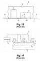
- FIG. 1Fshows a typical lapping machine 70 .
- the slider bar 52is held along the first cut surface 54 by a jig 72 .
- the jig 72is contacted by pistons 74 at various bending points 76 along the length of the jig 72 .
- Pistons 74may be, for example, dual action air cylinders, and are configured to deflect the jig 72 at the bending points 76 by a particular amount.
- a controller 78is used to regulate the operation of the pistons 74 .
- the slider bar 52is further oriented such that the second cut surface 56 lies substantially parallel to an upper surface 80 of a lapping plate 82 .
- an abrasive materialfor example a diamond slurry, is introduced between the second cut surface 56 of the slider bar 52 and the upper surface 80 of the lapping plate 82 .
- the slider bar 52 and the lapping plate 82are moved relative to each other within the plane defined by the second cut surface 56 and the upper surface 80 . This movement, along with the forces acting to press together the upper surface 80 and the second cut surface 56 and with the abrasive material placed therebetween, acts to abrasively lap the second cut surface 56 and thereby the read/write heads 60 .
- ELGelectronic lapping guide
- the ELGincludes a resistive element connected through leads to a device that monitors the resistance of the ELG.
- the resistive elementhas a height orthogonal to the lapping surface, next to which it is disposed, such that during the lapping operation, the resistive element is lapped away, increasing the resistance of the ELG.
- the resistance of the ELGreaches a predetermined resistance value corresponding to a desired stripe height/nose length in the nearby device, the lapping operation is stopped.
- a model that relates the measured resistance of an ELG to the remaining height of the resistive element of the ELGmay be used.
- To create such modelrequires multiple data points, which may be obtained by imaging cross-sections of partially-lapped ELGs to correlate the measured resistance of the ELGs with different remaining resistive element heights. This approach, however, relying as it does upon scanning electron microscopy, is complicated and slow, and can only be accomplished after a wafer has been cut into slider bars, and after the slider bars have been at least partially lapped.
- Various embodiments of the present inventionsolve the foregoing problems by providing a non-destructive wafer-level resistance modeling technique that correlates the resistance and inverse stripe height of a device, such as an ELG or even a read head, to be modeled based on measurements taken from an intact wafer.
- the approachinvolves a uniquely designed wafer in which otherwise similar devices in different regions have different initial stripe heights, whereby multiple data points correlating measured resistance and stripe height can be determined.
- a method for modeling devices in a wafercomprises the step of providing the wafer comprising a first plurality of devices having a track width TW and a first stripe height SH 1 , a second plurality of devices having the track width TW and a second stripe height SH 2 , and a third plurality of devices having the track width TW and a third stripe height SH 3 .
- the methodfurther comprises the steps of measuring resistance values for the first, second and third plurality of devices to obtain a data set correlating a stripe height and a resistance value for each of the first, second and third plurality of devices, and estimating a linear relationship between resistance and inverse stripe height for the first, second and third plurality of devices based on the data set.
- a wafercomprises a first plurality of devices having a track width TW and a first stripe height SH 1 , a second plurality of devices having the track width TW and a second stripe height SH 2 , and a third plurality of devices having the track width TW and a third stripe height SH 3 .
- the first, second and third plurality of devicesare arranged in corresponding first, second and third rows.
- FIG. 1Ais a partial cross-sectional front elevation view of a magnetic disk drive assembly
- FIG. 1Bis a top plan view taken along line 1 B- 1 B of FIG. 1A ;
- FIG. 1Cis a cross-sectional side view of a read-write head incorporating a shielded magnetoresistive read sensor
- FIG. 1Dis a plan view of a wafer including multiple slider bars that incorporate multiple read-write heads
- FIG. 1Eis a partial plan view of an individual one of the slider bars shown in FIG. 1D ;
- FIG. 1Fis a schematic diagram of a lapping machine in which a slider bar is positioned
- FIG. 2illustrates a wafer in accordance with one aspect of the subject disclosure
- FIG. 3illustrates a closer partial view of a wafer in accordance with one aspect of the subject disclosure.
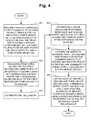
- FIG. 4is a flow chart illustrating a method of modeling devices in a wafer in accordance with one aspect of the subject disclosure.
- FIG. 2illustrates a wafer in accordance with one aspect of the subject disclosure, in which different regions of the wafer include devices with different stripe heights.
- region 201includes a plurality of ELGs 211 , 212 and 213 with a first resistive element stripe height
- region 202includes a plurality of ELGs with a second resistive element stripe height
- region 203includes a plurality of ELGs with a third resistive element stripe height.
- Region 201further includes a plurality of read heads 221 , 222 and 223 with a first reader stripe height, while region 202 includes a plurality of read heads with a second reader stripe height, and region 203 includes a plurality of read heads with a third reader stripe height.
- the remaining regions on the wafermay repeat this sequential pattern, such that each region (other than the outermost) abuts two regions with devices having different stripe heights.
- the regions of the wafermay be organized into rows that may be cut apart to form slider bars, such that each slider bar has ELGs with the same resistive element stripe height and read heads with the same reader stripe height. According to alternative embodiments of the subject disclosure, however, the regions may be organized in any one of a number of arrangements, including columns, grids, or the like.
- the scope of the present inventionis not limited to such an arrangement. Rather, as will be readily apparent to those of skill in the art in view of the subject disclosure, the present invention has application to wafers with any one of a number of different designs. For example, there may be more than three unique regions in a wafer, each having devices with different stripe heights. In accordance with one exemplary embodiment, for example, there may be devices with five different stripe heights in repeating sequences of five rows. Moreover, the rows may not necessarily be arranged in a repeating sequence, but may be arranged in any one of a number of other manners.
- the pattern of regionsmay be arranged such that each region abuts regions with devices having only incremental differences in stripe height (e.g., rows arranged with SH 1 , SH 2 , SH 3 , SH 4 , SH 3 , SH 2 , SH 1 , SH 2 , etc., instead of SH 1 , SH 2 , SH 3 , SH 4 , SH 1 , SH 2 , etc.).
- the waferincludes one or more devices, such as reader 311 and ELG 321 , which have stripe heights differing from similar devices in region 302 and 303 .
- reader 311 in region 301has a stripe height SH R1
- reader 312 in region 302has a stripe height SH R2
- reader 313 in region 303has a stripe height SH R3 , where SH R1 >SH R2 >SH R3 .
- ELG 321 in region 301has a resistive element 321 a with a stripe height SH G1
- ELG 322 in region 302has a resistive element 322 a with a stripe height SH G2
- ELG 323 in region 303has a resistive element 323 a with a stripe height SH G3 , where SH G1 >SH G2 >SH G3 .
- a measurement of the resistance of each ELGmay be made by probing the leads thereof (such as leads 321 b , 322 b and 323 b ) at the wafer level.
- a data set based on these measured resistances(R G1 for ELG 321 , R G2 for ELG 322 , and R G3 for ELG 323 ) and the inverse stripe height of each ELG (1/SH G1 for ELG 321 , 1/SH G2 for ELG 322 and 1/SH G3 for ELG 323 ) may be used to determine the slope and line values for this linear relationship as follows.
- the slope of the linemay be calculated according to the equation:
- the stripe heights of the ELGsmay be incremented in 1 micron steps from 4 microns to 8 microns.
- the stripe heights of the read headsmay be incremented in 30 nm steps from 150 nm to 270 nm.
- Such an arrangementmay facilitate the estimation of the stripe heights used in calculating the relationship between resistance and stripe height of the devices.
- the stripe heightsmay be estimated based upon resistance measurements made at the wafer level.
- a similar methodmay be used to estimate the stripe heights of devices when a wafer includes devices with more than three stripe heights separated by a fixed increment.
- a similar calculationcan be made to estimate the stripe heights.
- the resistance of the ELG at which lapping should be stoppedis easily calculated.
- the foregoing exemplary technique for modeling the relationship between the resistance and stripe height of a devicecan also be applied to devices other than ELGs.
- the slope and intercept of the lineare then calculated as set forth above for the ELG example.
- a wafermay include m pluralities of devices (e.g., ELGs or magnetoresistive read heads), each plurality of devices having a different stripe height than other ones of the plurality of devices, where m is any integer greater than or equal to 3.
- Providing a wafer with more than three different devicesmay enable evaluation of a correlation coefficient of the data set obtained as set forth above to assess whether the generated coefficients for the slope and intercept represent a good statistical fit to the data.
- a data set of values correlating measured resistances with estimated stripe heightsmay include information from every device on a wafer.
- the data setmay contain information from a subset of the devices on the wafer.
- multiple data setsmay be obtained to allow more local calibration to account for within-the-wafer (WIW) variation in fabrication.
- WIWwithin-the-wafer
- a correlation coefficientmay be calculated and used to detect erroneous data and re-calculate the required coefficients by either screening outliers or using the average of adjacent devices (e.g., devices in adjacent columns). This data can be evaluated at each column on a slider bar by either (i) calculating and assigning coefficient values in blocks of n bars where n>3, or (i) calculating and assigning coefficient values in rolling blocks of n bars where n>3.
- the flash fieldis an exposure field of the stepper, which may also be referred to as a stitch field.
- the majority of devicescan use coefficients generated by data measured within +/ ⁇ 2 rows of the device. Alternatively a single set of coefficients could be shared across all 5 devices. It should be noted that if n>5, the assumption that similar wafer level characteristics will apply to each member of the data set of n devices is progressively weakened due to the increased physical separation of the devices.
- the correlation coefficient r for a data setmay be calculated according to the formula
- r⁇ ( x - x _ ) ⁇ ( y - y _ ) ⁇ ( x - x _ ) 2 ⁇ ⁇ ( y - y _ ) 2 .
- one or more correlated stripe height and resistance valuesmay be removed from the data set before calculating the slope and intercept values.
- r 2is determined to be below a predetermined threshold, residuals within the data set may be calculated, such that the correlated stripe height and resistance value corresponding to the largest calculated residual can be rejected, and the Intercept, Slope and r 2 can be recalculated with the remaining data. If data is removed from the data set, the coefficients to be used at this location will be based on the remaining stripe height and resistance values in the data set.
- FIG. 4illustrates a method of modeling devices in a wafer in accordance with one aspect of the subject disclosure.
- the methodbegins with step 401 , in which a wafer is provided, the wafer comprising a first plurality of devices having a track width TW and a first stripe height SH 1 , a second plurality of devices having the track width TW and a second stripe height SH 2 , and a third plurality of devices having the track width TW and a third stripe height SH 3 .
- resistance values for the first, second and third plurality of devicesare measured to obtain a data set correlating a stripe height and a resistance value for each of the first, second and third plurality of devices.
- SH 1 , SH 2 , and SH 3may optionally be estimated based upon the measured resistance values.
- step 404a linear relationship between resistance and inverse stripe height is estimated for the first, second and third plurality of devices based on the data set.
- step 405the wafer is cut to separate first, second and third rows in which the corresponding first, second and third plurality of devices are arranged to form a first, a second and a third bar of devices.
- each of the first, second and third bar of devicesis lapped until a remaining stripe height for each of the corresponding plurality of devices therein is reached, based upon a measured change in resistance value and the estimated linear relationship.
- the foregoing techniques according to embodiments of the inventionmay be used in other applications in which it is desirable to characterize resistance versus strip height for controlling lapping and/or polishing of a write head, near field transducer or any other device.
- the techniquesmay be used to characterize resistance versus stripe height of ELGs for controlling lapping of a write head to achieve a desired nose length for the write head.
Landscapes
- Engineering & Computer Science (AREA)
- Manufacturing & Machinery (AREA)
- Magnetic Heads (AREA)
Abstract
Description
where n is a number of points in the data set, x is an inverse of a stripe height in the data set, and y is a resistance value in the data set. Similarly, the intercept of the line may be calculated according to the equation:
SH1+δH=SH3−δH=SH2=2δH((R3−R1)/(R3+R1−2R2))
wherein R1is a measured resistance value for one of the devices with the first stripe height SH1, R2is a measured resistance value for one of the devices with the second stripe height SH2, and R3is a measured resistance value for one of the devices with the third stripe height SH3.
If r2is determined to be below a predetermined threshold, one or more correlated stripe height and resistance values may be removed from the data set before calculating the slope and intercept values. In this regard, if r2is determined to be below a predetermined threshold, residuals within the data set may be calculated, such that the correlated stripe height and resistance value corresponding to the largest calculated residual can be rejected, and the Intercept, Slope and r2can be recalculated with the remaining data. If data is removed from the data set, the coefficients to be used at this location will be based on the remaining stripe height and resistance values in the data set.
Claims (20)
Priority Applications (1)
| Application Number | Priority Date | Filing Date | Title |
|---|---|---|---|
| US12/571,261US8307539B1 (en) | 2009-09-30 | 2009-09-30 | Method for modeling devices in a wafer |
Applications Claiming Priority (1)
| Application Number | Priority Date | Filing Date | Title |
|---|---|---|---|
| US12/571,261US8307539B1 (en) | 2009-09-30 | 2009-09-30 | Method for modeling devices in a wafer |
Publications (1)
| Publication Number | Publication Date |
|---|---|
| US8307539B1true US8307539B1 (en) | 2012-11-13 |
Family
ID=47114388
Family Applications (1)
| Application Number | Title | Priority Date | Filing Date |
|---|---|---|---|
| US12/571,261Expired - Fee RelatedUS8307539B1 (en) | 2009-09-30 | 2009-09-30 | Method for modeling devices in a wafer |
Country Status (1)
| Country | Link |
|---|---|
| US (1) | US8307539B1 (en) |
Cited By (137)
| Publication number | Priority date | Publication date | Assignee | Title |
|---|---|---|---|---|
| US8443510B1 (en) | 2009-05-28 | 2013-05-21 | Western Digital (Fremont), Llc | Method for utilizing an electronic lapping guide for a beveled pole in a magnetic recording transducer |
| US8717709B1 (en) | 2009-05-27 | 2014-05-06 | Western Digital (Fremont), Llc | System for calibrating an electronic lapping guide for a beveled pole in a magnetic recording transducer |
| US8830628B1 (en) | 2009-02-23 | 2014-09-09 | Western Digital (Fremont), Llc | Method and system for providing a perpendicular magnetic recording head |
| US8879207B1 (en) | 2011-12-20 | 2014-11-04 | Western Digital (Fremont), Llc | Method for providing a side shield for a magnetic recording transducer using an air bridge |
| US8883017B1 (en) | 2013-03-12 | 2014-11-11 | Western Digital (Fremont), Llc | Method and system for providing a read transducer having seamless interfaces |
| US8917581B1 (en) | 2013-12-18 | 2014-12-23 | Western Digital Technologies, Inc. | Self-anneal process for a near field transducer and chimney in a hard disk drive assembly |
| US8923102B1 (en) | 2013-07-16 | 2014-12-30 | Western Digital (Fremont), Llc | Optical grating coupling for interferometric waveguides in heat assisted magnetic recording heads |
| US8947985B1 (en) | 2013-07-16 | 2015-02-03 | Western Digital (Fremont), Llc | Heat assisted magnetic recording transducers having a recessed pole |
| US8953422B1 (en) | 2014-06-10 | 2015-02-10 | Western Digital (Fremont), Llc | Near field transducer using dielectric waveguide core with fine ridge feature |
| US8958272B1 (en) | 2014-06-10 | 2015-02-17 | Western Digital (Fremont), Llc | Interfering near field transducer for energy assisted magnetic recording |
| US8971160B1 (en) | 2013-12-19 | 2015-03-03 | Western Digital (Fremont), Llc | Near field transducer with high refractive index pin for heat assisted magnetic recording |
| US8970988B1 (en) | 2013-12-31 | 2015-03-03 | Western Digital (Fremont), Llc | Electric gaps and method for making electric gaps for multiple sensor arrays |
| US8976635B1 (en) | 2014-06-10 | 2015-03-10 | Western Digital (Fremont), Llc | Near field transducer driven by a transverse electric waveguide for energy assisted magnetic recording |
| US8980109B1 (en) | 2012-12-11 | 2015-03-17 | Western Digital (Fremont), Llc | Method for providing a magnetic recording transducer using a combined main pole and side shield CMP for a wraparound shield scheme |
| US8982508B1 (en) | 2011-10-31 | 2015-03-17 | Western Digital (Fremont), Llc | Method for providing a side shield for a magnetic recording transducer |
| US8984740B1 (en) | 2012-11-30 | 2015-03-24 | Western Digital (Fremont), Llc | Process for providing a magnetic recording transducer having a smooth magnetic seed layer |
| US8988825B1 (en) | 2014-02-28 | 2015-03-24 | Western Digital (Fremont, LLC | Method for fabricating a magnetic writer having half-side shields |
| US8988812B1 (en) | 2013-11-27 | 2015-03-24 | Western Digital (Fremont), Llc | Multi-sensor array configuration for a two-dimensional magnetic recording (TDMR) operation |
| US8995087B1 (en) | 2006-11-29 | 2015-03-31 | Western Digital (Fremont), Llc | Perpendicular magnetic recording write head having a wrap around shield |
| US8993217B1 (en) | 2013-04-04 | 2015-03-31 | Western Digital (Fremont), Llc | Double exposure technique for high resolution disk imaging |
| US9001628B1 (en) | 2013-12-16 | 2015-04-07 | Western Digital (Fremont), Llc | Assistant waveguides for evaluating main waveguide coupling efficiency and diode laser alignment tolerances for hard disk |
| US9001467B1 (en) | 2014-03-05 | 2015-04-07 | Western Digital (Fremont), Llc | Method for fabricating side shields in a magnetic writer |
| US8997832B1 (en) | 2010-11-23 | 2015-04-07 | Western Digital (Fremont), Llc | Method of fabricating micrometer scale components |
| US9007879B1 (en) | 2014-06-10 | 2015-04-14 | Western Digital (Fremont), Llc | Interfering near field transducer having a wide metal bar feature for energy assisted magnetic recording |
| US9007719B1 (en) | 2013-10-23 | 2015-04-14 | Western Digital (Fremont), Llc | Systems and methods for using double mask techniques to achieve very small features |
| US9007725B1 (en) | 2014-10-07 | 2015-04-14 | Western Digital (Fremont), Llc | Sensor with positive coupling between dual ferromagnetic free layer laminates |
| US9013836B1 (en) | 2013-04-02 | 2015-04-21 | Western Digital (Fremont), Llc | Method and system for providing an antiferromagnetically coupled return pole |
| US9042057B1 (en) | 2013-01-09 | 2015-05-26 | Western Digital (Fremont), Llc | Methods for providing magnetic storage elements with high magneto-resistance using Heusler alloys |
| US9042051B2 (en) | 2013-08-15 | 2015-05-26 | Western Digital (Fremont), Llc | Gradient write gap for perpendicular magnetic recording writer |
| US9042052B1 (en) | 2014-06-23 | 2015-05-26 | Western Digital (Fremont), Llc | Magnetic writer having a partially shunted coil |
| US9042058B1 (en) | 2013-10-17 | 2015-05-26 | Western Digital Technologies, Inc. | Shield designed for middle shields in a multiple sensor array |
| US9042208B1 (en) | 2013-03-11 | 2015-05-26 | Western Digital Technologies, Inc. | Disk drive measuring fly height by applying a bias voltage to an electrically insulated write component of a head |
| US9053735B1 (en) | 2014-06-20 | 2015-06-09 | Western Digital (Fremont), Llc | Method for fabricating a magnetic writer using a full-film metal planarization |
| US9064507B1 (en) | 2009-07-31 | 2015-06-23 | Western Digital (Fremont), Llc | Magnetic etch-stop layer for magnetoresistive read heads |
| US9064527B1 (en) | 2013-04-12 | 2015-06-23 | Western Digital (Fremont), Llc | High order tapered waveguide for use in a heat assisted magnetic recording head |
| US9065043B1 (en) | 2012-06-29 | 2015-06-23 | Western Digital (Fremont), Llc | Tunnel magnetoresistance read head with narrow shield-to-shield spacing |
| US9064528B1 (en) | 2013-05-17 | 2015-06-23 | Western Digital Technologies, Inc. | Interferometric waveguide usable in shingled heat assisted magnetic recording in the absence of a near-field transducer |
| US9070381B1 (en) | 2013-04-12 | 2015-06-30 | Western Digital (Fremont), Llc | Magnetic recording read transducer having a laminated free layer |
| US9082423B1 (en) | 2013-12-18 | 2015-07-14 | Western Digital (Fremont), Llc | Magnetic recording write transducer having an improved trailing surface profile |
| US9087527B1 (en) | 2014-10-28 | 2015-07-21 | Western Digital (Fremont), Llc | Apparatus and method for middle shield connection in magnetic recording transducers |
| US9087534B1 (en) | 2011-12-20 | 2015-07-21 | Western Digital (Fremont), Llc | Method and system for providing a read transducer having soft and hard magnetic bias structures |
| US9093087B2 (en) | 2013-09-16 | 2015-07-28 | International Business Machines Corporation | Apparatus with a lapping guide within a span of the transducer array |
| US9093639B2 (en) | 2012-02-21 | 2015-07-28 | Western Digital (Fremont), Llc | Methods for manufacturing a magnetoresistive structure utilizing heating and cooling |
| US9104107B1 (en) | 2013-04-03 | 2015-08-11 | Western Digital (Fremont), Llc | DUV photoresist process |
| US9111558B1 (en) | 2014-03-14 | 2015-08-18 | Western Digital (Fremont), Llc | System and method of diffractive focusing of light in a waveguide |
| US9111550B1 (en) | 2014-12-04 | 2015-08-18 | Western Digital (Fremont), Llc | Write transducer having a magnetic buffer layer spaced between a side shield and a write pole by non-magnetic layers |
| US9111564B1 (en) | 2013-04-02 | 2015-08-18 | Western Digital (Fremont), Llc | Magnetic recording writer having a main pole with multiple flare angles |
| US9123362B1 (en) | 2011-03-22 | 2015-09-01 | Western Digital (Fremont), Llc | Methods for assembling an electrically assisted magnetic recording (EAMR) head |
| US9123374B1 (en) | 2015-02-12 | 2015-09-01 | Western Digital (Fremont), Llc | Heat assisted magnetic recording writer having an integrated polarization rotation plate |
| US9123358B1 (en) | 2012-06-11 | 2015-09-01 | Western Digital (Fremont), Llc | Conformal high moment side shield seed layer for perpendicular magnetic recording writer |
| US9123359B1 (en) | 2010-12-22 | 2015-09-01 | Western Digital (Fremont), Llc | Magnetic recording transducer with sputtered antiferromagnetic coupling trilayer between plated ferromagnetic shields and method of fabrication |
| US9135937B1 (en) | 2014-05-09 | 2015-09-15 | Western Digital (Fremont), Llc | Current modulation on laser diode for energy assisted magnetic recording transducer |
| US9135930B1 (en) | 2014-03-06 | 2015-09-15 | Western Digital (Fremont), Llc | Method for fabricating a magnetic write pole using vacuum deposition |
| US9142233B1 (en) | 2014-02-28 | 2015-09-22 | Western Digital (Fremont), Llc | Heat assisted magnetic recording writer having a recessed pole |
| US9147408B1 (en) | 2013-12-19 | 2015-09-29 | Western Digital (Fremont), Llc | Heated AFM layer deposition and cooling process for TMR magnetic recording sensor with high pinning field |
| US9147404B1 (en) | 2015-03-31 | 2015-09-29 | Western Digital (Fremont), Llc | Method and system for providing a read transducer having a dual free layer |
| US9153260B1 (en) | 2008-03-27 | 2015-10-06 | Western Digital (Fremont), Llc | Electronic lapping guide in a magnetic recording transducer |
| US9153255B1 (en) | 2014-03-05 | 2015-10-06 | Western Digital (Fremont), Llc | Method for fabricating a magnetic writer having an asymmetric gap and shields |
| US9183854B2 (en) | 2014-02-24 | 2015-11-10 | Western Digital (Fremont), Llc | Method to make interferometric taper waveguide for HAMR light delivery |
| US9190085B1 (en) | 2014-03-12 | 2015-11-17 | Western Digital (Fremont), Llc | Waveguide with reflective grating for localized energy intensity |
| US9190079B1 (en) | 2014-09-22 | 2015-11-17 | Western Digital (Fremont), Llc | Magnetic write pole having engineered radius of curvature and chisel angle profiles |
| US9194692B1 (en) | 2013-12-06 | 2015-11-24 | Western Digital (Fremont), Llc | Systems and methods for using white light interferometry to measure undercut of a bi-layer structure |
| US9202480B2 (en) | 2009-10-14 | 2015-12-01 | Western Digital (Fremont), LLC. | Double patterning hard mask for damascene perpendicular magnetic recording (PMR) writer |
| US9202493B1 (en) | 2014-02-28 | 2015-12-01 | Western Digital (Fremont), Llc | Method of making an ultra-sharp tip mode converter for a HAMR head |
| US9213322B1 (en) | 2012-08-16 | 2015-12-15 | Western Digital (Fremont), Llc | Methods for providing run to run process control using a dynamic tuner |
| US9214172B2 (en) | 2013-10-23 | 2015-12-15 | Western Digital (Fremont), Llc | Method of manufacturing a magnetic read head |
| US9214165B1 (en) | 2014-12-18 | 2015-12-15 | Western Digital (Fremont), Llc | Magnetic writer having a gradient in saturation magnetization of the shields |
| US9214169B1 (en) | 2014-06-20 | 2015-12-15 | Western Digital (Fremont), Llc | Magnetic recording read transducer having a laminated free layer |
| US9230565B1 (en) | 2014-06-24 | 2016-01-05 | Western Digital (Fremont), Llc | Magnetic shield for magnetic recording head |
| US9236560B1 (en) | 2014-12-08 | 2016-01-12 | Western Digital (Fremont), Llc | Spin transfer torque tunneling magnetoresistive device having a laminated free layer with perpendicular magnetic anisotropy |
| US9245543B1 (en) | 2010-06-25 | 2016-01-26 | Western Digital (Fremont), Llc | Method for providing an energy assisted magnetic recording head having a laser integrally mounted to the slider |
| US9245562B1 (en) | 2015-03-30 | 2016-01-26 | Western Digital (Fremont), Llc | Magnetic recording writer with a composite main pole |
| US9245545B1 (en) | 2013-04-12 | 2016-01-26 | Wester Digital (Fremont), Llc | Short yoke length coils for magnetic heads in disk drives |
| US9251813B1 (en) | 2009-04-19 | 2016-02-02 | Western Digital (Fremont), Llc | Method of making a magnetic recording head |
| US9263067B1 (en) | 2013-05-29 | 2016-02-16 | Western Digital (Fremont), Llc | Process for making PMR writer with constant side wall angle |
| US9263071B1 (en) | 2015-03-31 | 2016-02-16 | Western Digital (Fremont), Llc | Flat NFT for heat assisted magnetic recording |
| US9269382B1 (en) | 2012-06-29 | 2016-02-23 | Western Digital (Fremont), Llc | Method and system for providing a read transducer having improved pinning of the pinned layer at higher recording densities |
| US9275657B1 (en) | 2013-08-14 | 2016-03-01 | Western Digital (Fremont), Llc | Process for making PMR writer with non-conformal side gaps |
| US9280990B1 (en) | 2013-12-11 | 2016-03-08 | Western Digital (Fremont), Llc | Method for fabricating a magnetic writer using multiple etches |
| US9286919B1 (en) | 2014-12-17 | 2016-03-15 | Western Digital (Fremont), Llc | Magnetic writer having a dual side gap |
| US9283651B2 (en) | 2013-09-06 | 2016-03-15 | Seagate Technology Llc | Apparatus including electrical lapping guide and methods of using the same |
| US9287494B1 (en) | 2013-06-28 | 2016-03-15 | Western Digital (Fremont), Llc | Magnetic tunnel junction (MTJ) with a magnesium oxide tunnel barrier |
| US9305583B1 (en) | 2014-02-18 | 2016-04-05 | Western Digital (Fremont), Llc | Method for fabricating a magnetic writer using multiple etches of damascene materials |
| US9312064B1 (en) | 2015-03-02 | 2016-04-12 | Western Digital (Fremont), Llc | Method to fabricate a magnetic head including ion milling of read gap using dual layer hard mask |
| US9318130B1 (en) | 2013-07-02 | 2016-04-19 | Western Digital (Fremont), Llc | Method to fabricate tunneling magnetic recording heads with extended pinned layer |
| US9336814B1 (en) | 2013-03-12 | 2016-05-10 | Western Digital (Fremont), Llc | Inverse tapered waveguide for use in a heat assisted magnetic recording head |
| US9343087B1 (en) | 2014-12-21 | 2016-05-17 | Western Digital (Fremont), Llc | Method for fabricating a magnetic writer having half shields |
| US9343098B1 (en) | 2013-08-23 | 2016-05-17 | Western Digital (Fremont), Llc | Method for providing a heat assisted magnetic recording transducer having protective pads |
| US9343086B1 (en) | 2013-09-11 | 2016-05-17 | Western Digital (Fremont), Llc | Magnetic recording write transducer having an improved sidewall angle profile |
| US9349394B1 (en) | 2013-10-18 | 2016-05-24 | Western Digital (Fremont), Llc | Method for fabricating a magnetic writer having a gradient side gap |
| US9349392B1 (en) | 2012-05-24 | 2016-05-24 | Western Digital (Fremont), Llc | Methods for improving adhesion on dielectric substrates |
| US9361913B1 (en) | 2013-06-03 | 2016-06-07 | Western Digital (Fremont), Llc | Recording read heads with a multi-layer AFM layer methods and apparatuses |
| US9361914B1 (en) | 2014-06-18 | 2016-06-07 | Western Digital (Fremont), Llc | Magnetic sensor with thin capping layer |
| US9368134B1 (en) | 2010-12-16 | 2016-06-14 | Western Digital (Fremont), Llc | Method and system for providing an antiferromagnetically coupled writer |
| US9384763B1 (en) | 2015-03-26 | 2016-07-05 | Western Digital (Fremont), Llc | Dual free layer magnetic reader having a rear bias structure including a soft bias layer |
| US9384765B1 (en) | 2015-09-24 | 2016-07-05 | Western Digital (Fremont), Llc | Method and system for providing a HAMR writer having improved optical efficiency |
| US9387568B1 (en)* | 2013-02-27 | 2016-07-12 | Western Digital Technologies, Inc. | Systems and methods for correcting fabrication error in magnetic recording heads using magnetic write width measurements |
| US9396743B1 (en) | 2014-02-28 | 2016-07-19 | Western Digital (Fremont), Llc | Systems and methods for controlling soft bias thickness for tunnel magnetoresistance readers |
| US9396742B1 (en) | 2012-11-30 | 2016-07-19 | Western Digital (Fremont), Llc | Magnetoresistive sensor for a magnetic storage system read head, and fabrication method thereof |
| US9406331B1 (en) | 2013-06-17 | 2016-08-02 | Western Digital (Fremont), Llc | Method for making ultra-narrow read sensor and read transducer device resulting therefrom |
| US9424866B1 (en) | 2015-09-24 | 2016-08-23 | Western Digital (Fremont), Llc | Heat assisted magnetic recording write apparatus having a dielectric gap |
| US9431047B1 (en) | 2013-05-01 | 2016-08-30 | Western Digital (Fremont), Llc | Method for providing an improved AFM reader shield |
| US9431038B1 (en) | 2015-06-29 | 2016-08-30 | Western Digital (Fremont), Llc | Method for fabricating a magnetic write pole having an improved sidewall angle profile |
| US9431032B1 (en) | 2013-08-14 | 2016-08-30 | Western Digital (Fremont), Llc | Electrical connection arrangement for a multiple sensor array usable in two-dimensional magnetic recording |
| US9431031B1 (en) | 2015-03-24 | 2016-08-30 | Western Digital (Fremont), Llc | System and method for magnetic transducers having multiple sensors and AFC shields |
| US9431039B1 (en) | 2013-05-21 | 2016-08-30 | Western Digital (Fremont), Llc | Multiple sensor array usable in two-dimensional magnetic recording |
| US9437251B1 (en) | 2014-12-22 | 2016-09-06 | Western Digital (Fremont), Llc | Apparatus and method having TDMR reader to reader shunts |
| US9443541B1 (en) | 2015-03-24 | 2016-09-13 | Western Digital (Fremont), Llc | Magnetic writer having a gradient in saturation magnetization of the shields and return pole |
| US9441938B1 (en) | 2013-10-08 | 2016-09-13 | Western Digital (Fremont), Llc | Test structures for measuring near field transducer disc length |
| US9449625B1 (en) | 2014-12-24 | 2016-09-20 | Western Digital (Fremont), Llc | Heat assisted magnetic recording head having a plurality of diffusion barrier layers |
| US9449621B1 (en) | 2015-03-26 | 2016-09-20 | Western Digital (Fremont), Llc | Dual free layer magnetic reader having a rear bias structure having a high aspect ratio |
| US9472216B1 (en) | 2015-09-23 | 2016-10-18 | Western Digital (Fremont), Llc | Differential dual free layer magnetic reader |
| US9484051B1 (en) | 2015-11-09 | 2016-11-01 | The Provost, Fellows, Foundation Scholars and the other members of Board, of the College of the Holy and Undivided Trinity of Queen Elizabeth near Dublin | Method and system for reducing undesirable reflections in a HAMR write apparatus |
| US9508372B1 (en) | 2015-06-03 | 2016-11-29 | Western Digital (Fremont), Llc | Shingle magnetic writer having a low sidewall angle pole |
| US9508365B1 (en) | 2015-06-24 | 2016-11-29 | Western Digital (Fremont), LLC. | Magnetic reader having a crystal decoupling structure |
| US9508363B1 (en) | 2014-06-17 | 2016-11-29 | Western Digital (Fremont), Llc | Method for fabricating a magnetic write pole having a leading edge bevel |
| US9530443B1 (en) | 2015-06-25 | 2016-12-27 | Western Digital (Fremont), Llc | Method for fabricating a magnetic recording device having a high aspect ratio structure |
| US9564150B1 (en) | 2015-11-24 | 2017-02-07 | Western Digital (Fremont), Llc | Magnetic read apparatus having an improved read sensor isolation circuit |
| US9595273B1 (en) | 2015-09-30 | 2017-03-14 | Western Digital (Fremont), Llc | Shingle magnetic writer having nonconformal shields |
| US9646639B2 (en) | 2015-06-26 | 2017-05-09 | Western Digital (Fremont), Llc | Heat assisted magnetic recording writer having integrated polarization rotation waveguides |
| US9666214B1 (en) | 2015-09-23 | 2017-05-30 | Western Digital (Fremont), Llc | Free layer magnetic reader that may have a reduced shield-to-shield spacing |
| US9721595B1 (en) | 2014-12-04 | 2017-08-01 | Western Digital (Fremont), Llc | Method for providing a storage device |
| US9741366B1 (en) | 2014-12-18 | 2017-08-22 | Western Digital (Fremont), Llc | Method for fabricating a magnetic writer having a gradient in saturation magnetization of the shields |
| US9740805B1 (en) | 2015-12-01 | 2017-08-22 | Western Digital (Fremont), Llc | Method and system for detecting hotspots for photolithographically-defined devices |
| US9754611B1 (en) | 2015-11-30 | 2017-09-05 | Western Digital (Fremont), Llc | Magnetic recording write apparatus having a stepped conformal trailing shield |
| US9767831B1 (en) | 2015-12-01 | 2017-09-19 | Western Digital (Fremont), Llc | Magnetic writer having convex trailing surface pole and conformal write gap |
| US9786301B1 (en) | 2014-12-02 | 2017-10-10 | Western Digital (Fremont), Llc | Apparatuses and methods for providing thin shields in a multiple sensor array |
| US9799351B1 (en) | 2015-11-30 | 2017-10-24 | Western Digital (Fremont), Llc | Short yoke length writer having assist coils |
| US9812155B1 (en) | 2015-11-23 | 2017-11-07 | Western Digital (Fremont), Llc | Method and system for fabricating high junction angle read sensors |
| US9842615B1 (en) | 2015-06-26 | 2017-12-12 | Western Digital (Fremont), Llc | Magnetic reader having a nonmagnetic insertion layer for the pinning layer |
| US9858951B1 (en) | 2015-12-01 | 2018-01-02 | Western Digital (Fremont), Llc | Method for providing a multilayer AFM layer in a read sensor |
| US9881638B1 (en) | 2014-12-17 | 2018-01-30 | Western Digital (Fremont), Llc | Method for providing a near-field transducer (NFT) for a heat assisted magnetic recording (HAMR) device |
| US9934811B1 (en) | 2014-03-07 | 2018-04-03 | Western Digital (Fremont), Llc | Methods for controlling stray fields of magnetic features using magneto-elastic anisotropy |
| US9953670B1 (en) | 2015-11-10 | 2018-04-24 | Western Digital (Fremont), Llc | Method and system for providing a HAMR writer including a multi-mode interference device |
| US10037770B1 (en) | 2015-11-12 | 2018-07-31 | Western Digital (Fremont), Llc | Method for providing a magnetic recording write apparatus having a seamless pole |
| US10074387B1 (en) | 2014-12-21 | 2018-09-11 | Western Digital (Fremont), Llc | Method and system for providing a read transducer having symmetric antiferromagnetically coupled shields |
| US11810602B2 (en) | 2021-09-09 | 2023-11-07 | International Business Machines Corporation | Mechanism to shift the head span of a tape head at a wafer level |
Citations (79)
| Publication number | Priority date | Publication date | Assignee | Title |
|---|---|---|---|---|
| US4157497A (en) | 1978-01-05 | 1979-06-05 | Rockwell International Corporation | Qualification test of gallium arsenide |
| US4670732A (en) | 1985-08-15 | 1987-06-02 | International Business Machines | Electrical lapping guide resistor |
| US4675986A (en) | 1985-07-29 | 1987-06-30 | International Business Machines | Electrical lapping guide for controlling the batch fabrication of thin film magnetic transducers |
| US5065483A (en) | 1991-02-19 | 1991-11-19 | International Business Machines Corporation | Method of lapping magnetic recording heads |
| US5210667A (en) | 1991-02-19 | 1993-05-11 | International Business Machines Corporation | Magnetic recording heads employing multiple lapping guides |
| US5361547A (en) | 1992-08-28 | 1994-11-08 | International Business Machines Corporation | Ultimate inductive head integrated lapping system |
| US5678086A (en) | 1996-07-22 | 1997-10-14 | Eastman Kodak Company | Patterned multi-track thin film heads for image area record/reproduce on magnetics-on-film |
| US5722155A (en) | 1996-01-11 | 1998-03-03 | Seagate Technology, Inc. | Machining guide method for magnetic recording reproduce heads |
| US5742995A (en)* | 1996-05-24 | 1998-04-28 | Seagate Technology, Inc. | Method to predict an accurate MR sensor dimension when viewed from abs |
| US5772493A (en) | 1995-07-31 | 1998-06-30 | Read-Rite Corporation | Method and apparatus for controlling the lapping of magnetic heads |
| US5876264A (en) | 1997-04-25 | 1999-03-02 | International Business Machines Corporation | Deposition process windage calibration |
| US6027397A (en) | 1997-04-25 | 2000-02-22 | International Business Machines Corporation | Dual element lapping guide system |
| JP2000067408A (en) | 1998-08-25 | 2000-03-03 | Fujitsu Ltd | Manufacturing method of magnetic head |
| US6047224A (en) | 1996-04-10 | 2000-04-04 | Seagate Techology, Inc. | Machining guide for magnetic recording reproduce heads |
| US6083081A (en) | 1997-08-07 | 2000-07-04 | Tdk Corporation | Lapping control sensor for magnetoresistive effect head, lapping control method using the sensor and manufacturing method of the sensor |
| US6193584B1 (en) | 1999-05-27 | 2001-02-27 | Read-Rite Corporation | Apparatus and method of device stripe height control |
| US20010004800A1 (en) | 1997-10-28 | 2001-06-28 | Tdk Corporation | Method for manufacturing thin-film magnetic head and manufacturing system of the head |
| US6288870B1 (en) | 1998-01-13 | 2001-09-11 | Quantum Corporation | Self-aligned metal film core multi-channel recording head for tape drives |
| US20010051491A1 (en) | 1996-12-13 | 2001-12-13 | Shanlin Hao | Multipoint bending apparatus for lapping heads of a data storage device |
| US20020012204A1 (en) | 2000-05-25 | 2002-01-31 | Zine-Eddine Boutaghou | Lapping sensor for recording heads |
| US6347983B1 (en) | 1999-06-09 | 2002-02-19 | Seagate Technology Llc | ELG for both MRE sensor height and resistance monitoring |
| US6364743B1 (en) | 1999-06-11 | 2002-04-02 | Seagate Technology Llc | Composite lapping monitor resistor |
| US6399401B1 (en) | 2001-07-24 | 2002-06-04 | Advanced Micro Devices, In. | Test structures for electrical linewidth measurement and processes for their formation |
| US20020173227A1 (en) | 2001-03-16 | 2002-11-21 | Lam Chuck Fai | Embedded lapping guide |
| US20030020467A1 (en) | 2001-07-30 | 2003-01-30 | Tdk Corporation | Lapping monitor element, combined magnetic transducer element and lapping monitor element, and method for manufacturing magnetic transducer element |
| US20030021069A1 (en) | 2001-07-30 | 2003-01-30 | Crawforth Linden James | Slider having integrated lapping guides |
| US6609948B1 (en) | 2000-11-27 | 2003-08-26 | International Business Machines Corporation | Method of making an electronic lapping guide (ELG) for lapping a read sensor |
| US6623330B2 (en) | 2001-02-08 | 2003-09-23 | Sae Magnetics (H. K.) Ltd. | Lapping sensor used in fabrication of magnetic head with magnetoresistive effect element and lapping control method using the sensor |
| US6674610B1 (en) | 2000-06-16 | 2004-01-06 | Western Digital (Fremont), Inc. | Thin film write head with universal coil design |
| US20040009739A1 (en) | 2002-07-12 | 2004-01-15 | Li-Yan Zhu | Dual-purpose lapping guide for the production of magneto-resistive heads |
| US6684171B2 (en) | 2002-04-22 | 2004-01-27 | International Business Machines Corporation | In-situ stripe height calibration of magneto resistive sensors |
| US6699102B2 (en) | 2001-01-12 | 2004-03-02 | International Business Machines Corporation | Lapping monitor for monitoring the lapping of transducers |
| US20040075942A1 (en) | 2002-05-30 | 2004-04-22 | Bajorek Christopher H. | Lapping a head while powered up to eliminate expansion of the head due to heating |
| US20040097173A1 (en) | 2002-11-19 | 2004-05-20 | International Business Machines Corporation | Onboard multiphase electronic lapping guide design for MR heads |
| US6793557B2 (en) | 2002-05-24 | 2004-09-21 | International Business Machines Corporation | Removable lapping guide for magnetic recording head and method of use |
| US6846222B2 (en) | 2003-03-04 | 2005-01-25 | Hitachi Global Storage Technologies Netherlands, B.V. | Multi-chambered, compliant apparatus for restraining workpiece and applying variable pressure thereto during lapping to improve flatness characteristics of workpiece |
| US20050023673A1 (en) | 2003-07-25 | 2005-02-03 | Stefan Nowak | Transistor module |
| US20050028354A1 (en) | 2000-06-16 | 2005-02-10 | Tdk Corporation | Device and method for measuring amount of grinding in magnetic head producing process |
| US20050070206A1 (en) | 2003-09-29 | 2005-03-31 | Prakash Kasiraj | Slider fabrication system for sliders with integrated electrical lapping guides |
| US6884148B1 (en) | 2004-05-26 | 2005-04-26 | Headway Technologies, Inc. | Independently controlled read and write head stripe height parameters in slider back end process |
| US20050180048A1 (en) | 2004-02-13 | 2005-08-18 | Hitachi Global Technologies Netherlands B.V. | Perpendicular magnetic recording head built using an air-bearing surface damascene process |
| US20050185345A1 (en) | 2004-02-20 | 2005-08-25 | Meng Ding | Electrical lapping guide embedded in a shield of a magnetic head |
| US6935923B2 (en) | 2003-03-12 | 2005-08-30 | Seagate Technology Llc | Sensor stripe encapsulation layer in a read/write head |
| US20050219752A1 (en) | 2004-04-05 | 2005-10-06 | Alps Electric Co., Ltd. | Vertical recording magnetic head and method of manufacturing the same |
| US6982042B2 (en) | 2003-02-28 | 2006-01-03 | Hitachi Global Storage Technologies Netherlands, B.V. | Ion bombardment of electrical lapping guides to decrease noise during lapping process |
| US20060028770A1 (en) | 2004-08-03 | 2006-02-09 | Hitachi Global Storage Technologies Netherlands B.V. | Magnetic head with electro lapping guide and manufacturing method |
| US20060034021A1 (en) | 2004-08-13 | 2006-02-16 | Wu Andrew L | Methods of manufacturing magnetic heads with reference and monitoring devices |
| US20060044683A1 (en) | 2004-09-01 | 2006-03-02 | Sae Magnetics (H.K.) Ltd. | Thin film magnetic head structure, method of manufacturing the same, and method of manufacturing thin film magnetic head |
| US20060103990A1 (en) | 2004-11-16 | 2006-05-18 | Sae Magnetics (H.K.) Ltd. | Magnetic head manufacturing method, magnetic head, angle setting device and lapping device |
| US20060126222A1 (en) | 2004-10-20 | 2006-06-15 | Tdk Corporation | Thin film magnetic head, method of manufacturing the same, and magnetic recording apparatus |
| US20060139802A1 (en) | 2004-12-28 | 2006-06-29 | Headway Technologies, Inc. | Method of manufacturing magnetic head, and magnetic head sub-structure |
| US20060168798A1 (en) | 2005-01-31 | 2006-08-03 | Kabushiki Kaisha Toshiba | Method of lapping row bar in which perpendicular magnetic heads are formed and lapping machine |
| US7139152B2 (en) | 2003-10-20 | 2006-11-21 | Quantum Corporation | Servo methods and systems using existing data structures and optical masks |
| US7149061B2 (en) | 2001-07-31 | 2006-12-12 | Hitachi, Ltd. | Magnetic head with electro-lapping guide |
| US20070070543A1 (en) | 2005-09-29 | 2007-03-29 | Hitachi Global Storage Technologies Netherlands B.V. | Lapping method and station to achieve tight dimension controls for both read and write elements of magnetic recording heads and magnetic storage device formed thereby |
| US7244169B2 (en) | 2004-09-30 | 2007-07-17 | Hitachi Global Storage Technologies Netherlands Bv | In-line contiguous resistive lapping guide for magnetic sensors |
| US7245459B2 (en) | 2004-09-30 | 2007-07-17 | Hitachi Global Storage Technologies Netherlands Bv | Critically exposed lapping of magnetic sensors for target signal output |
| US7272883B2 (en) | 2003-08-29 | 2007-09-25 | Hitachi Global Storage Technologies Netherlands B.V. | Methods of forming an electrical connection in a magnetic head using a damascene process |
| US20070246761A1 (en) | 2006-04-19 | 2007-10-25 | Beach Robert S | Electrical lapping guides made from tunneling magnetoresistive (tmr) material |
| US20080072418A1 (en) | 2006-09-01 | 2008-03-27 | Hitachi Global Storage Technologies Netherlands B.V. | Method for manufacturing a magnetic head slider |
| US7360296B2 (en) | 2004-09-30 | 2008-04-22 | Hitachi Global Storage Technologies Netherlands B.V. | Method for reducing damage to sliders during lapping |
| US20080144215A1 (en) | 2006-12-15 | 2008-06-19 | Hitachi Global Storage Technologies | Electrical lapping guide for flare point control and trailing shield throat height in a perpendicular magnetic write head |
| US7393262B2 (en) | 2001-08-23 | 2008-07-01 | International Business Machines Corporation | Apparatus including pin adapter for air bearing surface (ABS) lapping |
| US7422511B2 (en)* | 2006-06-12 | 2008-09-09 | Sae Magnetics (H.K.) Ltd. | Element for detecting the amount of lapping having a resistive film electrically connected to the substrate |
| US20080273275A1 (en) | 2007-05-04 | 2008-11-06 | Jeffrey S Lille | Fabricating a write head with multiple electronic lapping guides |
| US20090152235A1 (en) | 2007-12-13 | 2009-06-18 | Wen-Chien David Hsiao | Method of manufacturing a perpendicular magnetic write head with stepped trailing magnetic shield with electrical lapping guide control |
| US7551406B1 (en) | 2005-07-01 | 2009-06-23 | Western Digital (Fremont), Llc | Dual electrical lapping guides with common bonding pad |
| US7554767B1 (en) | 2005-07-01 | 2009-06-30 | Western Digital (Fremont), Llc | Electrical lapping guide disposed laterally relative to a shield pedestal |
| US20090211081A1 (en) | 2008-02-25 | 2009-08-27 | Boone Jr Thomas D | Controlled lapping for an abs damascene process |
| US7603762B2 (en) | 2006-12-15 | 2009-10-20 | Hitachi Global Storage Technologies Netherlands B.V. | Optical lapping guide for use in the manufacture of perpendicular magnetic write heads |
| US20090268348A1 (en) | 2008-04-28 | 2009-10-29 | Christian Rene Bonhote | Write head lapping guide about aligned to a non-magnetic layer surrounding a write pole and a method for making the same |
| US7643250B2 (en) | 2006-01-27 | 2010-01-05 | Hitachi Global Storage Technologies Netherlands B.V. | Pad slider design for on-slider ELGs |
| US7716814B2 (en)* | 2007-02-05 | 2010-05-18 | Headway Technologies, Inc. | Method of manufacturing magnetic head, and magnetic head substructure |
| US20100162556A1 (en) | 2008-12-30 | 2010-07-01 | Unal Murat Guruz | Electrical lapping guide for improving magnetic core width in a magnetic recording head |
| US20100165513A1 (en) | 2008-12-31 | 2010-07-01 | Christian Rene Bonhote | Write head with self-align layer and a method for making the same |
| US7770281B2 (en) | 2007-05-10 | 2010-08-10 | Hitachi Global Storage Technologies Netherlands B.V. | Method for redefining the trailing shield throat height in a perpendicular magnetic recording write head |
| US20100208391A1 (en) | 2009-02-13 | 2010-08-19 | Seagate Technology Llc | Lapping Guides For Magnetic Recording Heads |
| US8151441B1 (en) | 2008-03-27 | 2012-04-10 | Western Digital (Fremont), Llc | Method for providing and utilizing an electronic lapping guide in a magnetic recording transducer |
| US8165709B1 (en) | 2009-02-26 | 2012-04-24 | Western Digital (Fremont), Llc | Four pad self-calibrating electronic lapping guide |
- 2009
- 2009-09-30USUS12/571,261patent/US8307539B1/ennot_activeExpired - Fee Related
Patent Citations (104)
| Publication number | Priority date | Publication date | Assignee | Title |
|---|---|---|---|---|
| US4157497A (en) | 1978-01-05 | 1979-06-05 | Rockwell International Corporation | Qualification test of gallium arsenide |
| US4675986A (en) | 1985-07-29 | 1987-06-30 | International Business Machines | Electrical lapping guide for controlling the batch fabrication of thin film magnetic transducers |
| US4670732A (en) | 1985-08-15 | 1987-06-02 | International Business Machines | Electrical lapping guide resistor |
| US5065483A (en) | 1991-02-19 | 1991-11-19 | International Business Machines Corporation | Method of lapping magnetic recording heads |
| US5210667A (en) | 1991-02-19 | 1993-05-11 | International Business Machines Corporation | Magnetic recording heads employing multiple lapping guides |
| US5361547A (en) | 1992-08-28 | 1994-11-08 | International Business Machines Corporation | Ultimate inductive head integrated lapping system |
| US5597340A (en) | 1992-08-28 | 1997-01-28 | International Business Machines Corporation | Ultimate inductive head integrated lapping system |
| US5772493A (en) | 1995-07-31 | 1998-06-30 | Read-Rite Corporation | Method and apparatus for controlling the lapping of magnetic heads |
| US5722155A (en) | 1996-01-11 | 1998-03-03 | Seagate Technology, Inc. | Machining guide method for magnetic recording reproduce heads |
| US6047224A (en) | 1996-04-10 | 2000-04-04 | Seagate Techology, Inc. | Machining guide for magnetic recording reproduce heads |
| US5742995A (en)* | 1996-05-24 | 1998-04-28 | Seagate Technology, Inc. | Method to predict an accurate MR sensor dimension when viewed from abs |
| US6003361A (en) | 1996-05-24 | 1999-12-21 | Seagate Technology, Inc. | System for predicting accurate MR sensor height |
| US5678086A (en) | 1996-07-22 | 1997-10-14 | Eastman Kodak Company | Patterned multi-track thin film heads for image area record/reproduce on magnetics-on-film |
| US20010051491A1 (en) | 1996-12-13 | 2001-12-13 | Shanlin Hao | Multipoint bending apparatus for lapping heads of a data storage device |
| US6475064B2 (en) | 1996-12-13 | 2002-11-05 | Seagate Technology Llc | Multipoint bending apparatus for lapping heads of a data storage device |
| US5876264A (en) | 1997-04-25 | 1999-03-02 | International Business Machines Corporation | Deposition process windage calibration |
| US6027397A (en) | 1997-04-25 | 2000-02-22 | International Business Machines Corporation | Dual element lapping guide system |
| US6083081A (en) | 1997-08-07 | 2000-07-04 | Tdk Corporation | Lapping control sensor for magnetoresistive effect head, lapping control method using the sensor and manufacturing method of the sensor |
| US20010004800A1 (en) | 1997-10-28 | 2001-06-28 | Tdk Corporation | Method for manufacturing thin-film magnetic head and manufacturing system of the head |
| US6288870B1 (en) | 1998-01-13 | 2001-09-11 | Quantum Corporation | Self-aligned metal film core multi-channel recording head for tape drives |
| JP2000067408A (en) | 1998-08-25 | 2000-03-03 | Fujitsu Ltd | Manufacturing method of magnetic head |
| US6532646B2 (en) | 1998-08-25 | 2003-03-18 | Fujitsu Limited | Method of manufacturing magnetic head |
| US6193584B1 (en) | 1999-05-27 | 2001-02-27 | Read-Rite Corporation | Apparatus and method of device stripe height control |
| US6347983B1 (en) | 1999-06-09 | 2002-02-19 | Seagate Technology Llc | ELG for both MRE sensor height and resistance monitoring |
| US6364743B1 (en) | 1999-06-11 | 2002-04-02 | Seagate Technology Llc | Composite lapping monitor resistor |
| US6760197B2 (en) | 2000-05-25 | 2004-07-06 | Seagate Technology Llc | Lapping sensor for recording heads having guide element kept |
| US20020012204A1 (en) | 2000-05-25 | 2002-01-31 | Zine-Eddine Boutaghou | Lapping sensor for recording heads |
| US6674610B1 (en) | 2000-06-16 | 2004-01-06 | Western Digital (Fremont), Inc. | Thin film write head with universal coil design |
| US20050028354A1 (en) | 2000-06-16 | 2005-02-10 | Tdk Corporation | Device and method for measuring amount of grinding in magnetic head producing process |
| US6609948B1 (en) | 2000-11-27 | 2003-08-26 | International Business Machines Corporation | Method of making an electronic lapping guide (ELG) for lapping a read sensor |
| US6699102B2 (en) | 2001-01-12 | 2004-03-02 | International Business Machines Corporation | Lapping monitor for monitoring the lapping of transducers |
| US6623330B2 (en) | 2001-02-08 | 2003-09-23 | Sae Magnetics (H. K.) Ltd. | Lapping sensor used in fabrication of magnetic head with magnetoresistive effect element and lapping control method using the sensor |
| US20020173227A1 (en) | 2001-03-16 | 2002-11-21 | Lam Chuck Fai | Embedded lapping guide |
| US6950289B2 (en) | 2001-03-16 | 2005-09-27 | Lafe Computer Magnetics Ltd. | Embedded lapping guide for a magnetic head cluster |
| US20040179310A1 (en) | 2001-03-16 | 2004-09-16 | Lam Chuck Fai | Embedded lapping guide |
| US6399401B1 (en) | 2001-07-24 | 2002-06-04 | Advanced Micro Devices, In. | Test structures for electrical linewidth measurement and processes for their formation |
| US20030021069A1 (en) | 2001-07-30 | 2003-01-30 | Crawforth Linden James | Slider having integrated lapping guides |
| US6728067B2 (en) | 2001-07-30 | 2004-04-27 | Hitachi Global Storage Technologies Netherlands B.V. | Slider having integrated lapping guides |
| US20030020467A1 (en) | 2001-07-30 | 2003-01-30 | Tdk Corporation | Lapping monitor element, combined magnetic transducer element and lapping monitor element, and method for manufacturing magnetic transducer element |
| US7287316B2 (en) | 2001-07-30 | 2007-10-30 | Tdk Corporation | Lapping monitor device, system and method |
| US7149061B2 (en) | 2001-07-31 | 2006-12-12 | Hitachi, Ltd. | Magnetic head with electro-lapping guide |
| US20070008660A1 (en) | 2001-07-31 | 2007-01-11 | Hitachi Global Storage Technologies Japan Ltd. | Magnetic head and method of manufacturing the same |
| US7268976B2 (en) | 2001-07-31 | 2007-09-11 | Hitachi, Ltd. | Magnetic head and method of manufacturing the same |
| US7393262B2 (en) | 2001-08-23 | 2008-07-01 | International Business Machines Corporation | Apparatus including pin adapter for air bearing surface (ABS) lapping |
| US6684171B2 (en) | 2002-04-22 | 2004-01-27 | International Business Machines Corporation | In-situ stripe height calibration of magneto resistive sensors |
| US6793557B2 (en) | 2002-05-24 | 2004-09-21 | International Business Machines Corporation | Removable lapping guide for magnetic recording head and method of use |
| US6857937B2 (en) | 2002-05-30 | 2005-02-22 | Komag, Inc. | Lapping a head while powered up to eliminate expansion of the head due to heating |
| US20050164607A1 (en) | 2002-05-30 | 2005-07-28 | Bajorek Christopher H. | Lapping a head while powered up to eliminate expansion of the head due to heating |
| US20040075942A1 (en) | 2002-05-30 | 2004-04-22 | Bajorek Christopher H. | Lapping a head while powered up to eliminate expansion of the head due to heating |
| US20040009739A1 (en) | 2002-07-12 | 2004-01-15 | Li-Yan Zhu | Dual-purpose lapping guide for the production of magneto-resistive heads |
| US6758722B2 (en) | 2002-07-12 | 2004-07-06 | Sae Magentics, (H.K.) Ltd. | Dual-purpose lapping guide for the production of magneto-resistive heads |
| US6786803B2 (en)* | 2002-11-19 | 2004-09-07 | International Business Machines Corporation | Onboard multiphase electronic lapping guide design for MR heads |
| US20040097173A1 (en) | 2002-11-19 | 2004-05-20 | International Business Machines Corporation | Onboard multiphase electronic lapping guide design for MR heads |
| US7333300B2 (en) | 2003-02-28 | 2008-02-19 | Hitachi Global Storage Technologies Netherlands B.V. | Magnetoresistive device with lapping guide treated to eliminate magnetoresistive effect thereof |
| US6982042B2 (en) | 2003-02-28 | 2006-01-03 | Hitachi Global Storage Technologies Netherlands, B.V. | Ion bombardment of electrical lapping guides to decrease noise during lapping process |
| US20060027528A1 (en) | 2003-02-28 | 2006-02-09 | Hitachi Global Storage Technologies | Ion bombardment of electrical lapping guides to decrease noise during lapping process |
| US6846222B2 (en) | 2003-03-04 | 2005-01-25 | Hitachi Global Storage Technologies Netherlands, B.V. | Multi-chambered, compliant apparatus for restraining workpiece and applying variable pressure thereto during lapping to improve flatness characteristics of workpiece |
| US6935923B2 (en) | 2003-03-12 | 2005-08-30 | Seagate Technology Llc | Sensor stripe encapsulation layer in a read/write head |
| US20050023673A1 (en) | 2003-07-25 | 2005-02-03 | Stefan Nowak | Transistor module |
| US7272883B2 (en) | 2003-08-29 | 2007-09-25 | Hitachi Global Storage Technologies Netherlands B.V. | Methods of forming an electrical connection in a magnetic head using a damascene process |
| US20050070206A1 (en) | 2003-09-29 | 2005-03-31 | Prakash Kasiraj | Slider fabrication system for sliders with integrated electrical lapping guides |
| US7014530B2 (en) | 2003-09-29 | 2006-03-21 | Hitachi Global Storage Technologies Netherlands B.V. | Slider fabrication system for sliders with integrated electrical lapping guides |
| US7139152B2 (en) | 2003-10-20 | 2006-11-21 | Quantum Corporation | Servo methods and systems using existing data structures and optical masks |
| US7271982B2 (en) | 2004-02-13 | 2007-09-18 | Hitachi Global Storage Technologies Netherlands B.V. | Perpendicular magnetic recording head built using an air-bearing surface damascene process |
| US20050180048A1 (en) | 2004-02-13 | 2005-08-18 | Hitachi Global Technologies Netherlands B.V. | Perpendicular magnetic recording head built using an air-bearing surface damascene process |
| US20050185345A1 (en) | 2004-02-20 | 2005-08-25 | Meng Ding | Electrical lapping guide embedded in a shield of a magnetic head |
| US7206172B2 (en) | 2004-02-20 | 2007-04-17 | Hitachi Global Storage Technologies Netherlands B.V. | Electrical lapping guide embedded in a shield of a magnetic head |
| US20050219752A1 (en) | 2004-04-05 | 2005-10-06 | Alps Electric Co., Ltd. | Vertical recording magnetic head and method of manufacturing the same |
| US6884148B1 (en) | 2004-05-26 | 2005-04-26 | Headway Technologies, Inc. | Independently controlled read and write head stripe height parameters in slider back end process |
| US20060028770A1 (en) | 2004-08-03 | 2006-02-09 | Hitachi Global Storage Technologies Netherlands B.V. | Magnetic head with electro lapping guide and manufacturing method |
| US20080013219A1 (en) | 2004-08-13 | 2008-01-17 | Quantum Corporation | Methods of manufacturing magnetic heads with reference and monitoring devices |
| US20060034021A1 (en) | 2004-08-13 | 2006-02-16 | Wu Andrew L | Methods of manufacturing magnetic heads with reference and monitoring devices |
| US20060044683A1 (en) | 2004-09-01 | 2006-03-02 | Sae Magnetics (H.K.) Ltd. | Thin film magnetic head structure, method of manufacturing the same, and method of manufacturing thin film magnetic head |
| US7359152B2 (en) | 2004-09-01 | 2008-04-15 | Sae Magnetics, (H.K.) Ltd. | Thin film magnetic head structure, method of manufacturing the same, and method of manufacturing thin film magnetic head |
| US7244169B2 (en) | 2004-09-30 | 2007-07-17 | Hitachi Global Storage Technologies Netherlands Bv | In-line contiguous resistive lapping guide for magnetic sensors |
| US7360296B2 (en) | 2004-09-30 | 2008-04-22 | Hitachi Global Storage Technologies Netherlands B.V. | Method for reducing damage to sliders during lapping |
| US7245459B2 (en) | 2004-09-30 | 2007-07-17 | Hitachi Global Storage Technologies Netherlands Bv | Critically exposed lapping of magnetic sensors for target signal output |
| US20060126222A1 (en) | 2004-10-20 | 2006-06-15 | Tdk Corporation | Thin film magnetic head, method of manufacturing the same, and magnetic recording apparatus |
| US20060103990A1 (en) | 2004-11-16 | 2006-05-18 | Sae Magnetics (H.K.) Ltd. | Magnetic head manufacturing method, magnetic head, angle setting device and lapping device |
| US20060139802A1 (en) | 2004-12-28 | 2006-06-29 | Headway Technologies, Inc. | Method of manufacturing magnetic head, and magnetic head sub-structure |
| US20060168798A1 (en) | 2005-01-31 | 2006-08-03 | Kabushiki Kaisha Toshiba | Method of lapping row bar in which perpendicular magnetic heads are formed and lapping machine |
| US7551406B1 (en) | 2005-07-01 | 2009-06-23 | Western Digital (Fremont), Llc | Dual electrical lapping guides with common bonding pad |
| US7554767B1 (en) | 2005-07-01 | 2009-06-30 | Western Digital (Fremont), Llc | Electrical lapping guide disposed laterally relative to a shield pedestal |
| US20070070543A1 (en) | 2005-09-29 | 2007-03-29 | Hitachi Global Storage Technologies Netherlands B.V. | Lapping method and station to achieve tight dimension controls for both read and write elements of magnetic recording heads and magnetic storage device formed thereby |
| US7643250B2 (en) | 2006-01-27 | 2010-01-05 | Hitachi Global Storage Technologies Netherlands B.V. | Pad slider design for on-slider ELGs |
| US20070246761A1 (en) | 2006-04-19 | 2007-10-25 | Beach Robert S | Electrical lapping guides made from tunneling magnetoresistive (tmr) material |
| US7564110B2 (en) | 2006-04-19 | 2009-07-21 | Hitachi Global Storage Technologies Netherlands B.V. | Electrical lapping guides made from tunneling magnetoresistive (TMR) material |
| US7422511B2 (en)* | 2006-06-12 | 2008-09-09 | Sae Magnetics (H.K.) Ltd. | Element for detecting the amount of lapping having a resistive film electrically connected to the substrate |
| US20080072418A1 (en) | 2006-09-01 | 2008-03-27 | Hitachi Global Storage Technologies Netherlands B.V. | Method for manufacturing a magnetic head slider |
| US7603762B2 (en) | 2006-12-15 | 2009-10-20 | Hitachi Global Storage Technologies Netherlands B.V. | Optical lapping guide for use in the manufacture of perpendicular magnetic write heads |
| US7788796B2 (en) | 2006-12-15 | 2010-09-07 | Hitachi Global Storage Technologies Netherlands B.V. | Method FPR manufacturing a magnetic write head |
| US20080144215A1 (en) | 2006-12-15 | 2008-06-19 | Hitachi Global Storage Technologies | Electrical lapping guide for flare point control and trailing shield throat height in a perpendicular magnetic write head |
| US7716814B2 (en)* | 2007-02-05 | 2010-05-18 | Headway Technologies, Inc. | Method of manufacturing magnetic head, and magnetic head substructure |
| US20080273275A1 (en) | 2007-05-04 | 2008-11-06 | Jeffrey S Lille | Fabricating a write head with multiple electronic lapping guides |
| US7861400B2 (en) | 2007-05-04 | 2011-01-04 | Hitachi Global Storage Technologies Netherlands, B.V. | Fabricating a write head with multiple electronic lapping guides |
| US7770281B2 (en) | 2007-05-10 | 2010-08-10 | Hitachi Global Storage Technologies Netherlands B.V. | Method for redefining the trailing shield throat height in a perpendicular magnetic recording write head |
| US20090152235A1 (en) | 2007-12-13 | 2009-06-18 | Wen-Chien David Hsiao | Method of manufacturing a perpendicular magnetic write head with stepped trailing magnetic shield with electrical lapping guide control |
| US20090211081A1 (en) | 2008-02-25 | 2009-08-27 | Boone Jr Thomas D | Controlled lapping for an abs damascene process |
| US8151441B1 (en) | 2008-03-27 | 2012-04-10 | Western Digital (Fremont), Llc | Method for providing and utilizing an electronic lapping guide in a magnetic recording transducer |
| US20090268348A1 (en) | 2008-04-28 | 2009-10-29 | Christian Rene Bonhote | Write head lapping guide about aligned to a non-magnetic layer surrounding a write pole and a method for making the same |
| US20100162556A1 (en) | 2008-12-30 | 2010-07-01 | Unal Murat Guruz | Electrical lapping guide for improving magnetic core width in a magnetic recording head |
| US20100165513A1 (en) | 2008-12-31 | 2010-07-01 | Christian Rene Bonhote | Write head with self-align layer and a method for making the same |
| US20100208391A1 (en) | 2009-02-13 | 2010-08-19 | Seagate Technology Llc | Lapping Guides For Magnetic Recording Heads |
| US8165709B1 (en) | 2009-02-26 | 2012-04-24 | Western Digital (Fremont), Llc | Four pad self-calibrating electronic lapping guide |
Non-Patent Citations (1)
| Title |
|---|
| Matsushita, et al., "Elaborate Precision Machining Technologies for Creating High Added Value at Low Cost", Fujitsu Sci. Tech. J., 43, 1, pp. 67-75, Jan. 2007. |
Cited By (161)
| Publication number | Priority date | Publication date | Assignee | Title |
|---|---|---|---|---|
| US8995087B1 (en) | 2006-11-29 | 2015-03-31 | Western Digital (Fremont), Llc | Perpendicular magnetic recording write head having a wrap around shield |
| US9153260B1 (en) | 2008-03-27 | 2015-10-06 | Western Digital (Fremont), Llc | Electronic lapping guide in a magnetic recording transducer |
| US8830628B1 (en) | 2009-02-23 | 2014-09-09 | Western Digital (Fremont), Llc | Method and system for providing a perpendicular magnetic recording head |
| US9251813B1 (en) | 2009-04-19 | 2016-02-02 | Western Digital (Fremont), Llc | Method of making a magnetic recording head |
| US8717709B1 (en) | 2009-05-27 | 2014-05-06 | Western Digital (Fremont), Llc | System for calibrating an electronic lapping guide for a beveled pole in a magnetic recording transducer |
| US8443510B1 (en) | 2009-05-28 | 2013-05-21 | Western Digital (Fremont), Llc | Method for utilizing an electronic lapping guide for a beveled pole in a magnetic recording transducer |
| US9064507B1 (en) | 2009-07-31 | 2015-06-23 | Western Digital (Fremont), Llc | Magnetic etch-stop layer for magnetoresistive read heads |
| US9202480B2 (en) | 2009-10-14 | 2015-12-01 | Western Digital (Fremont), LLC. | Double patterning hard mask for damascene perpendicular magnetic recording (PMR) writer |
| US9245543B1 (en) | 2010-06-25 | 2016-01-26 | Western Digital (Fremont), Llc | Method for providing an energy assisted magnetic recording head having a laser integrally mounted to the slider |
| US9672847B2 (en) | 2010-11-23 | 2017-06-06 | Western Digital (Fremont), Llc | Micrometer scale components |
| US8997832B1 (en) | 2010-11-23 | 2015-04-07 | Western Digital (Fremont), Llc | Method of fabricating micrometer scale components |
| US9159345B1 (en) | 2010-11-23 | 2015-10-13 | Western Digital (Fremont), Llc | Micrometer scale components |
| US9368134B1 (en) | 2010-12-16 | 2016-06-14 | Western Digital (Fremont), Llc | Method and system for providing an antiferromagnetically coupled writer |
| US9123359B1 (en) | 2010-12-22 | 2015-09-01 | Western Digital (Fremont), Llc | Magnetic recording transducer with sputtered antiferromagnetic coupling trilayer between plated ferromagnetic shields and method of fabrication |
| US9123362B1 (en) | 2011-03-22 | 2015-09-01 | Western Digital (Fremont), Llc | Methods for assembling an electrically assisted magnetic recording (EAMR) head |
| US8982508B1 (en) | 2011-10-31 | 2015-03-17 | Western Digital (Fremont), Llc | Method for providing a side shield for a magnetic recording transducer |
| US9087534B1 (en) | 2011-12-20 | 2015-07-21 | Western Digital (Fremont), Llc | Method and system for providing a read transducer having soft and hard magnetic bias structures |
| US8879207B1 (en) | 2011-12-20 | 2014-11-04 | Western Digital (Fremont), Llc | Method for providing a side shield for a magnetic recording transducer using an air bridge |
| US9093639B2 (en) | 2012-02-21 | 2015-07-28 | Western Digital (Fremont), Llc | Methods for manufacturing a magnetoresistive structure utilizing heating and cooling |
| US9349392B1 (en) | 2012-05-24 | 2016-05-24 | Western Digital (Fremont), Llc | Methods for improving adhesion on dielectric substrates |
| US9940950B2 (en) | 2012-05-24 | 2018-04-10 | Western Digital (Fremont), Llc | Methods for improving adhesion on dielectric substrates |
| US9123358B1 (en) | 2012-06-11 | 2015-09-01 | Western Digital (Fremont), Llc | Conformal high moment side shield seed layer for perpendicular magnetic recording writer |
| US9065043B1 (en) | 2012-06-29 | 2015-06-23 | Western Digital (Fremont), Llc | Tunnel magnetoresistance read head with narrow shield-to-shield spacing |
| US9412400B2 (en) | 2012-06-29 | 2016-08-09 | Western Digital (Fremont), Llc | Tunnel magnetoresistance read head with narrow shield-to-shield spacing |
| US9269382B1 (en) | 2012-06-29 | 2016-02-23 | Western Digital (Fremont), Llc | Method and system for providing a read transducer having improved pinning of the pinned layer at higher recording densities |
| US9213322B1 (en) | 2012-08-16 | 2015-12-15 | Western Digital (Fremont), Llc | Methods for providing run to run process control using a dynamic tuner |
| US8984740B1 (en) | 2012-11-30 | 2015-03-24 | Western Digital (Fremont), Llc | Process for providing a magnetic recording transducer having a smooth magnetic seed layer |
| US9396742B1 (en) | 2012-11-30 | 2016-07-19 | Western Digital (Fremont), Llc | Magnetoresistive sensor for a magnetic storage system read head, and fabrication method thereof |
| US8980109B1 (en) | 2012-12-11 | 2015-03-17 | Western Digital (Fremont), Llc | Method for providing a magnetic recording transducer using a combined main pole and side shield CMP for a wraparound shield scheme |
| US9042057B1 (en) | 2013-01-09 | 2015-05-26 | Western Digital (Fremont), Llc | Methods for providing magnetic storage elements with high magneto-resistance using Heusler alloys |
| US9387568B1 (en)* | 2013-02-27 | 2016-07-12 | Western Digital Technologies, Inc. | Systems and methods for correcting fabrication error in magnetic recording heads using magnetic write width measurements |
| US9042208B1 (en) | 2013-03-11 | 2015-05-26 | Western Digital Technologies, Inc. | Disk drive measuring fly height by applying a bias voltage to an electrically insulated write component of a head |
| US8883017B1 (en) | 2013-03-12 | 2014-11-11 | Western Digital (Fremont), Llc | Method and system for providing a read transducer having seamless interfaces |
| US9336814B1 (en) | 2013-03-12 | 2016-05-10 | Western Digital (Fremont), Llc | Inverse tapered waveguide for use in a heat assisted magnetic recording head |
| US9013836B1 (en) | 2013-04-02 | 2015-04-21 | Western Digital (Fremont), Llc | Method and system for providing an antiferromagnetically coupled return pole |
| US9111564B1 (en) | 2013-04-02 | 2015-08-18 | Western Digital (Fremont), Llc | Magnetic recording writer having a main pole with multiple flare angles |
| US9104107B1 (en) | 2013-04-03 | 2015-08-11 | Western Digital (Fremont), Llc | DUV photoresist process |
| US8993217B1 (en) | 2013-04-04 | 2015-03-31 | Western Digital (Fremont), Llc | Double exposure technique for high resolution disk imaging |
| US9064527B1 (en) | 2013-04-12 | 2015-06-23 | Western Digital (Fremont), Llc | High order tapered waveguide for use in a heat assisted magnetic recording head |
| US9245545B1 (en) | 2013-04-12 | 2016-01-26 | Wester Digital (Fremont), Llc | Short yoke length coils for magnetic heads in disk drives |
| US9070381B1 (en) | 2013-04-12 | 2015-06-30 | Western Digital (Fremont), Llc | Magnetic recording read transducer having a laminated free layer |
| US9431047B1 (en) | 2013-05-01 | 2016-08-30 | Western Digital (Fremont), Llc | Method for providing an improved AFM reader shield |
| US9064528B1 (en) | 2013-05-17 | 2015-06-23 | Western Digital Technologies, Inc. | Interferometric waveguide usable in shingled heat assisted magnetic recording in the absence of a near-field transducer |
| US9431039B1 (en) | 2013-05-21 | 2016-08-30 | Western Digital (Fremont), Llc | Multiple sensor array usable in two-dimensional magnetic recording |
| US9263067B1 (en) | 2013-05-29 | 2016-02-16 | Western Digital (Fremont), Llc | Process for making PMR writer with constant side wall angle |
| US9361913B1 (en) | 2013-06-03 | 2016-06-07 | Western Digital (Fremont), Llc | Recording read heads with a multi-layer AFM layer methods and apparatuses |
| US9406331B1 (en) | 2013-06-17 | 2016-08-02 | Western Digital (Fremont), Llc | Method for making ultra-narrow read sensor and read transducer device resulting therefrom |
| US9287494B1 (en) | 2013-06-28 | 2016-03-15 | Western Digital (Fremont), Llc | Magnetic tunnel junction (MTJ) with a magnesium oxide tunnel barrier |
| US9318130B1 (en) | 2013-07-02 | 2016-04-19 | Western Digital (Fremont), Llc | Method to fabricate tunneling magnetic recording heads with extended pinned layer |
| US8923102B1 (en) | 2013-07-16 | 2014-12-30 | Western Digital (Fremont), Llc | Optical grating coupling for interferometric waveguides in heat assisted magnetic recording heads |
| US8947985B1 (en) | 2013-07-16 | 2015-02-03 | Western Digital (Fremont), Llc | Heat assisted magnetic recording transducers having a recessed pole |
| US9431032B1 (en) | 2013-08-14 | 2016-08-30 | Western Digital (Fremont), Llc | Electrical connection arrangement for a multiple sensor array usable in two-dimensional magnetic recording |
| US9275657B1 (en) | 2013-08-14 | 2016-03-01 | Western Digital (Fremont), Llc | Process for making PMR writer with non-conformal side gaps |
| US9042051B2 (en) | 2013-08-15 | 2015-05-26 | Western Digital (Fremont), Llc | Gradient write gap for perpendicular magnetic recording writer |
| US9343098B1 (en) | 2013-08-23 | 2016-05-17 | Western Digital (Fremont), Llc | Method for providing a heat assisted magnetic recording transducer having protective pads |
| US9283651B2 (en) | 2013-09-06 | 2016-03-15 | Seagate Technology Llc | Apparatus including electrical lapping guide and methods of using the same |
| US9343086B1 (en) | 2013-09-11 | 2016-05-17 | Western Digital (Fremont), Llc | Magnetic recording write transducer having an improved sidewall angle profile |
| US9093087B2 (en) | 2013-09-16 | 2015-07-28 | International Business Machines Corporation | Apparatus with a lapping guide within a span of the transducer array |
| US9441938B1 (en) | 2013-10-08 | 2016-09-13 | Western Digital (Fremont), Llc | Test structures for measuring near field transducer disc length |
| US9042058B1 (en) | 2013-10-17 | 2015-05-26 | Western Digital Technologies, Inc. | Shield designed for middle shields in a multiple sensor array |
| US9349394B1 (en) | 2013-10-18 | 2016-05-24 | Western Digital (Fremont), Llc | Method for fabricating a magnetic writer having a gradient side gap |
| US9830936B2 (en) | 2013-10-23 | 2017-11-28 | Western Digital (Fremont), Llc | Magnetic read head with antiferromagentic layer |
| US9007719B1 (en) | 2013-10-23 | 2015-04-14 | Western Digital (Fremont), Llc | Systems and methods for using double mask techniques to achieve very small features |
| US9214172B2 (en) | 2013-10-23 | 2015-12-15 | Western Digital (Fremont), Llc | Method of manufacturing a magnetic read head |
| US8988812B1 (en) | 2013-11-27 | 2015-03-24 | Western Digital (Fremont), Llc | Multi-sensor array configuration for a two-dimensional magnetic recording (TDMR) operation |
| US9194692B1 (en) | 2013-12-06 | 2015-11-24 | Western Digital (Fremont), Llc | Systems and methods for using white light interferometry to measure undercut of a bi-layer structure |
| US9280990B1 (en) | 2013-12-11 | 2016-03-08 | Western Digital (Fremont), Llc | Method for fabricating a magnetic writer using multiple etches |
| US9001628B1 (en) | 2013-12-16 | 2015-04-07 | Western Digital (Fremont), Llc | Assistant waveguides for evaluating main waveguide coupling efficiency and diode laser alignment tolerances for hard disk |
| US9082423B1 (en) | 2013-12-18 | 2015-07-14 | Western Digital (Fremont), Llc | Magnetic recording write transducer having an improved trailing surface profile |
| US8917581B1 (en) | 2013-12-18 | 2014-12-23 | Western Digital Technologies, Inc. | Self-anneal process for a near field transducer and chimney in a hard disk drive assembly |
| US8971160B1 (en) | 2013-12-19 | 2015-03-03 | Western Digital (Fremont), Llc | Near field transducer with high refractive index pin for heat assisted magnetic recording |
| US9147408B1 (en) | 2013-12-19 | 2015-09-29 | Western Digital (Fremont), Llc | Heated AFM layer deposition and cooling process for TMR magnetic recording sensor with high pinning field |
| US8970988B1 (en) | 2013-12-31 | 2015-03-03 | Western Digital (Fremont), Llc | Electric gaps and method for making electric gaps for multiple sensor arrays |
| US9305583B1 (en) | 2014-02-18 | 2016-04-05 | Western Digital (Fremont), Llc | Method for fabricating a magnetic writer using multiple etches of damascene materials |
| US9183854B2 (en) | 2014-02-24 | 2015-11-10 | Western Digital (Fremont), Llc | Method to make interferometric taper waveguide for HAMR light delivery |
| US9396743B1 (en) | 2014-02-28 | 2016-07-19 | Western Digital (Fremont), Llc | Systems and methods for controlling soft bias thickness for tunnel magnetoresistance readers |
| US8988825B1 (en) | 2014-02-28 | 2015-03-24 | Western Digital (Fremont, LLC | Method for fabricating a magnetic writer having half-side shields |
| US9142233B1 (en) | 2014-02-28 | 2015-09-22 | Western Digital (Fremont), Llc | Heat assisted magnetic recording writer having a recessed pole |
| US9202493B1 (en) | 2014-02-28 | 2015-12-01 | Western Digital (Fremont), Llc | Method of making an ultra-sharp tip mode converter for a HAMR head |
| US9001467B1 (en) | 2014-03-05 | 2015-04-07 | Western Digital (Fremont), Llc | Method for fabricating side shields in a magnetic writer |
| US9153255B1 (en) | 2014-03-05 | 2015-10-06 | Western Digital (Fremont), Llc | Method for fabricating a magnetic writer having an asymmetric gap and shields |
| US9349393B2 (en) | 2014-03-05 | 2016-05-24 | Western Digital (Fremont), Llc | Magnetic writer having an asymmetric gap and shields |
| US9135930B1 (en) | 2014-03-06 | 2015-09-15 | Western Digital (Fremont), Llc | Method for fabricating a magnetic write pole using vacuum deposition |
| US9934811B1 (en) | 2014-03-07 | 2018-04-03 | Western Digital (Fremont), Llc | Methods for controlling stray fields of magnetic features using magneto-elastic anisotropy |
| US9190085B1 (en) | 2014-03-12 | 2015-11-17 | Western Digital (Fremont), Llc | Waveguide with reflective grating for localized energy intensity |
| US9495984B2 (en) | 2014-03-12 | 2016-11-15 | Western Digital (Fremont), Llc | Waveguide with reflective grating for localized energy intensity |
| US9111558B1 (en) | 2014-03-14 | 2015-08-18 | Western Digital (Fremont), Llc | System and method of diffractive focusing of light in a waveguide |
| US9135937B1 (en) | 2014-05-09 | 2015-09-15 | Western Digital (Fremont), Llc | Current modulation on laser diode for energy assisted magnetic recording transducer |
| US8953422B1 (en) | 2014-06-10 | 2015-02-10 | Western Digital (Fremont), Llc | Near field transducer using dielectric waveguide core with fine ridge feature |
| US9007879B1 (en) | 2014-06-10 | 2015-04-14 | Western Digital (Fremont), Llc | Interfering near field transducer having a wide metal bar feature for energy assisted magnetic recording |
| US8958272B1 (en) | 2014-06-10 | 2015-02-17 | Western Digital (Fremont), Llc | Interfering near field transducer for energy assisted magnetic recording |
| US8976635B1 (en) | 2014-06-10 | 2015-03-10 | Western Digital (Fremont), Llc | Near field transducer driven by a transverse electric waveguide for energy assisted magnetic recording |
| US9311952B2 (en) | 2014-06-10 | 2016-04-12 | Western Digital (Fremont), Llc | Interfering near field transducer for energy assisted magnetic recording |
| US9159346B1 (en) | 2014-06-10 | 2015-10-13 | Western Digital (Fremont), Llc | Near field transducer using dielectric waveguide core with fine ridge feature |
| US9508363B1 (en) | 2014-06-17 | 2016-11-29 | Western Digital (Fremont), Llc | Method for fabricating a magnetic write pole having a leading edge bevel |
| US9361914B1 (en) | 2014-06-18 | 2016-06-07 | Western Digital (Fremont), Llc | Magnetic sensor with thin capping layer |
| US9214169B1 (en) | 2014-06-20 | 2015-12-15 | Western Digital (Fremont), Llc | Magnetic recording read transducer having a laminated free layer |
| US9053735B1 (en) | 2014-06-20 | 2015-06-09 | Western Digital (Fremont), Llc | Method for fabricating a magnetic writer using a full-film metal planarization |
| US9042052B1 (en) | 2014-06-23 | 2015-05-26 | Western Digital (Fremont), Llc | Magnetic writer having a partially shunted coil |
| US9230565B1 (en) | 2014-06-24 | 2016-01-05 | Western Digital (Fremont), Llc | Magnetic shield for magnetic recording head |
| US9190079B1 (en) | 2014-09-22 | 2015-11-17 | Western Digital (Fremont), Llc | Magnetic write pole having engineered radius of curvature and chisel angle profiles |
| US9007725B1 (en) | 2014-10-07 | 2015-04-14 | Western Digital (Fremont), Llc | Sensor with positive coupling between dual ferromagnetic free layer laminates |
| US9087527B1 (en) | 2014-10-28 | 2015-07-21 | Western Digital (Fremont), Llc | Apparatus and method for middle shield connection in magnetic recording transducers |
| US9786301B1 (en) | 2014-12-02 | 2017-10-10 | Western Digital (Fremont), Llc | Apparatuses and methods for providing thin shields in a multiple sensor array |
| US10460751B2 (en)* | 2014-12-04 | 2019-10-29 | Western Digital (Fremont), Llc | Stripe height lapping control structures for a multiple sensor array |
| US20180268847A1 (en)* | 2014-12-04 | 2018-09-20 | Western Digital (Fremont), Llc | Stripe height lapping control structures for a multiple sensor array |
| US9111550B1 (en) | 2014-12-04 | 2015-08-18 | Western Digital (Fremont), Llc | Write transducer having a magnetic buffer layer spaced between a side shield and a write pole by non-magnetic layers |
| US10008222B2 (en)* | 2014-12-04 | 2018-06-26 | Western Digital (Fremont), Llc | Stripe height lapping control structures for a multiple sensor array |
| US9721595B1 (en) | 2014-12-04 | 2017-08-01 | Western Digital (Fremont), Llc | Method for providing a storage device |
| US9705072B2 (en) | 2014-12-08 | 2017-07-11 | Western Digital (Fremont), Llc | Spin transfer torque tunneling magnetoresistive device having a laminated free layer with perpendicular magnetic anisotropy |
| US9236560B1 (en) | 2014-12-08 | 2016-01-12 | Western Digital (Fremont), Llc | Spin transfer torque tunneling magnetoresistive device having a laminated free layer with perpendicular magnetic anisotropy |
| US9286919B1 (en) | 2014-12-17 | 2016-03-15 | Western Digital (Fremont), Llc | Magnetic writer having a dual side gap |
| US9881638B1 (en) | 2014-12-17 | 2018-01-30 | Western Digital (Fremont), Llc | Method for providing a near-field transducer (NFT) for a heat assisted magnetic recording (HAMR) device |
| US10553241B2 (en) | 2014-12-17 | 2020-02-04 | Western Digital Technologies, Inc. | Near-field transducer (NFT) for a heat assisted magnetic recording (HAMR) device |
| US9741366B1 (en) | 2014-12-18 | 2017-08-22 | Western Digital (Fremont), Llc | Method for fabricating a magnetic writer having a gradient in saturation magnetization of the shields |
| US9214165B1 (en) | 2014-12-18 | 2015-12-15 | Western Digital (Fremont), Llc | Magnetic writer having a gradient in saturation magnetization of the shields |
| US9343087B1 (en) | 2014-12-21 | 2016-05-17 | Western Digital (Fremont), Llc | Method for fabricating a magnetic writer having half shields |
| US10074387B1 (en) | 2014-12-21 | 2018-09-11 | Western Digital (Fremont), Llc | Method and system for providing a read transducer having symmetric antiferromagnetically coupled shields |
| US9437251B1 (en) | 2014-12-22 | 2016-09-06 | Western Digital (Fremont), Llc | Apparatus and method having TDMR reader to reader shunts |
| US9449625B1 (en) | 2014-12-24 | 2016-09-20 | Western Digital (Fremont), Llc | Heat assisted magnetic recording head having a plurality of diffusion barrier layers |
| US9123374B1 (en) | 2015-02-12 | 2015-09-01 | Western Digital (Fremont), Llc | Heat assisted magnetic recording writer having an integrated polarization rotation plate |
| US9312064B1 (en) | 2015-03-02 | 2016-04-12 | Western Digital (Fremont), Llc | Method to fabricate a magnetic head including ion milling of read gap using dual layer hard mask |
| US9443541B1 (en) | 2015-03-24 | 2016-09-13 | Western Digital (Fremont), Llc | Magnetic writer having a gradient in saturation magnetization of the shields and return pole |
| US9754613B2 (en) | 2015-03-24 | 2017-09-05 | Western Digital (Fremont), Llc | Method for AFC shields for multiple sensor magnetic transducers and magnetic transducers having multiple sensors and AFC shields |
| US10115419B2 (en) | 2015-03-24 | 2018-10-30 | Western Digital (Fremont), Llc | Method for AFC shields for multiple sensor magnetic transducers and magnetic transducers having multiple sensors and AFC shields |
| US9431031B1 (en) | 2015-03-24 | 2016-08-30 | Western Digital (Fremont), Llc | System and method for magnetic transducers having multiple sensors and AFC shields |
| US9922672B1 (en) | 2015-03-26 | 2018-03-20 | Western Digital (Fremont), Llc | Dual free layer magnetic reader having a rear bias structure having a high aspect ratio |
| US9449621B1 (en) | 2015-03-26 | 2016-09-20 | Western Digital (Fremont), Llc | Dual free layer magnetic reader having a rear bias structure having a high aspect ratio |
| US9384763B1 (en) | 2015-03-26 | 2016-07-05 | Western Digital (Fremont), Llc | Dual free layer magnetic reader having a rear bias structure including a soft bias layer |
| US9245562B1 (en) | 2015-03-30 | 2016-01-26 | Western Digital (Fremont), Llc | Magnetic recording writer with a composite main pole |
| US9263071B1 (en) | 2015-03-31 | 2016-02-16 | Western Digital (Fremont), Llc | Flat NFT for heat assisted magnetic recording |
| US9147404B1 (en) | 2015-03-31 | 2015-09-29 | Western Digital (Fremont), Llc | Method and system for providing a read transducer having a dual free layer |
| US9508372B1 (en) | 2015-06-03 | 2016-11-29 | Western Digital (Fremont), Llc | Shingle magnetic writer having a low sidewall angle pole |
| US9508365B1 (en) | 2015-06-24 | 2016-11-29 | Western Digital (Fremont), LLC. | Magnetic reader having a crystal decoupling structure |
| US9530443B1 (en) | 2015-06-25 | 2016-12-27 | Western Digital (Fremont), Llc | Method for fabricating a magnetic recording device having a high aspect ratio structure |
| US9646639B2 (en) | 2015-06-26 | 2017-05-09 | Western Digital (Fremont), Llc | Heat assisted magnetic recording writer having integrated polarization rotation waveguides |
| US10242700B2 (en) | 2015-06-26 | 2019-03-26 | Western Digital (Fremont), Llc | Magnetic reader having a nonmagnetic insertion layer for the pinning layer |
| US10037773B2 (en) | 2015-06-26 | 2018-07-31 | Western Digital (Fremont), Llc | Heat assisted magnetic recording writer having integrated polarization rotation waveguides |
| US9842615B1 (en) | 2015-06-26 | 2017-12-12 | Western Digital (Fremont), Llc | Magnetic reader having a nonmagnetic insertion layer for the pinning layer |
| US9431038B1 (en) | 2015-06-29 | 2016-08-30 | Western Digital (Fremont), Llc | Method for fabricating a magnetic write pole having an improved sidewall angle profile |
| US10121501B2 (en) | 2015-09-23 | 2018-11-06 | Western Digital (Fremont), Llc | Free layer magnetic reader that may have a reduced shield-to-shield spacing |
| US9472216B1 (en) | 2015-09-23 | 2016-10-18 | Western Digital (Fremont), Llc | Differential dual free layer magnetic reader |
| US9666214B1 (en) | 2015-09-23 | 2017-05-30 | Western Digital (Fremont), Llc | Free layer magnetic reader that may have a reduced shield-to-shield spacing |
| US9384765B1 (en) | 2015-09-24 | 2016-07-05 | Western Digital (Fremont), Llc | Method and system for providing a HAMR writer having improved optical efficiency |
| US9424866B1 (en) | 2015-09-24 | 2016-08-23 | Western Digital (Fremont), Llc | Heat assisted magnetic recording write apparatus having a dielectric gap |
| US9595273B1 (en) | 2015-09-30 | 2017-03-14 | Western Digital (Fremont), Llc | Shingle magnetic writer having nonconformal shields |
| US9484051B1 (en) | 2015-11-09 | 2016-11-01 | The Provost, Fellows, Foundation Scholars and the other members of Board, of the College of the Holy and Undivided Trinity of Queen Elizabeth near Dublin | Method and system for reducing undesirable reflections in a HAMR write apparatus |
| US10381029B2 (en) | 2015-11-10 | 2019-08-13 | Western Digital (Fremont), Llc | Method and system for providing a HAMR writer including a multi-mode interference device |
| US9953670B1 (en) | 2015-11-10 | 2018-04-24 | Western Digital (Fremont), Llc | Method and system for providing a HAMR writer including a multi-mode interference device |
| US10037770B1 (en) | 2015-11-12 | 2018-07-31 | Western Digital (Fremont), Llc | Method for providing a magnetic recording write apparatus having a seamless pole |
| US9812155B1 (en) | 2015-11-23 | 2017-11-07 | Western Digital (Fremont), Llc | Method and system for fabricating high junction angle read sensors |
| US9564150B1 (en) | 2015-11-24 | 2017-02-07 | Western Digital (Fremont), Llc | Magnetic read apparatus having an improved read sensor isolation circuit |
| US9754611B1 (en) | 2015-11-30 | 2017-09-05 | Western Digital (Fremont), Llc | Magnetic recording write apparatus having a stepped conformal trailing shield |
| US10121495B2 (en) | 2015-11-30 | 2018-11-06 | Western Digital (Fremont), Llc | Magnetic recording write apparatus having a stepped conformal trailing shield |
| US9799351B1 (en) | 2015-11-30 | 2017-10-24 | Western Digital (Fremont), Llc | Short yoke length writer having assist coils |
| US9740805B1 (en) | 2015-12-01 | 2017-08-22 | Western Digital (Fremont), Llc | Method and system for detecting hotspots for photolithographically-defined devices |
| US9997177B2 (en) | 2015-12-01 | 2018-06-12 | Western Digital (Fremont), Llc | Magnetic writer having convex trailing surface pole and conformal write gap |
| US9767831B1 (en) | 2015-12-01 | 2017-09-19 | Western Digital (Fremont), Llc | Magnetic writer having convex trailing surface pole and conformal write gap |
| US9858951B1 (en) | 2015-12-01 | 2018-01-02 | Western Digital (Fremont), Llc | Method for providing a multilayer AFM layer in a read sensor |
| US11810602B2 (en) | 2021-09-09 | 2023-11-07 | International Business Machines Corporation | Mechanism to shift the head span of a tape head at a wafer level |
| US12073858B2 (en) | 2021-09-09 | 2024-08-27 | International Business Machines Corporation | Mechanism to shift the head span of a tape head at a wafer level |
Similar Documents
| Publication | Publication Date | Title |
|---|---|---|
| US8307539B1 (en) | Method for modeling devices in a wafer | |
| US6684171B2 (en) | In-situ stripe height calibration of magneto resistive sensors | |
| US6857937B2 (en) | Lapping a head while powered up to eliminate expansion of the head due to heating | |
| US6261165B1 (en) | Row carrier for precision lapping of disk drive heads and for handling of heads during the slider fab operation | |
| US8165709B1 (en) | Four pad self-calibrating electronic lapping guide | |
| CN100440319C (en) | Grinding method and grinding device for bar with vertical magnetic head formed inside | |
| US6884148B1 (en) | Independently controlled read and write head stripe height parameters in slider back end process | |
| US6347983B1 (en) | ELG for both MRE sensor height and resistance monitoring | |
| US7206172B2 (en) | Electrical lapping guide embedded in a shield of a magnetic head | |
| US6758722B2 (en) | Dual-purpose lapping guide for the production of magneto-resistive heads | |
| US20080013219A1 (en) | Methods of manufacturing magnetic heads with reference and monitoring devices | |
| EP1732064A2 (en) | Magnetic recording heads with bearing surface protections and methods of manufacture | |
| US8407882B2 (en) | Method for manufacturing thin film magnetic heads | |
| US8390962B2 (en) | Lapping method and station to achieve tight dimension controls for both read and write elements of magnetic recording heads and magnetic storage device formed thereby | |
| US7116519B2 (en) | Patterning of integrated closure for implementing pads connected to lapping elements | |
| US6515475B2 (en) | Determination of track width of magnetoresistive sensors during magnetic head fabrication using magnetic fields | |
| US6568992B1 (en) | Method for controlling MRE stripe height | |
| US6731110B2 (en) | Magneto-resistive device with built-in test structure and method for determining resistance and track width | |
| JP2007193902A (en) | Magnetic head inspection method, magnetic head manufacturing method, magnetic head, and magnetic disk device | |
| US20160071535A1 (en) | Methods of manufacturing magnetic heads using a trigger reader electronic lapping guide | |
| US6299507B1 (en) | Thin-film magnetic head manufacturing method and apparatus | |
| US11823712B2 (en) | Built-in resistance sensor for measuring slider level pole width at point “A” (PWA) for PMR/MAMR writers | |
| US20020066177A1 (en) | Method for manufacturing magneto-resistive effect type magnetic heads | |
| US6859678B1 (en) | Method and apparatus for manufacturing magnetoresistive element, software and system for controlling manufacturing of magnetoresistive element, software for estimating resistance value of magnetoresistive element, and computer system | |
| US10290314B1 (en) | Locating electrical contact pads on a slider body, and related row bars that include such slider bodies |
Legal Events
| Date | Code | Title | Description |
|---|---|---|---|
| AS | Assignment | Owner name:WESTERN DIGITAL (FREMONT), LLC, CALIFORNIA Free format text:ASSIGNMENT OF ASSIGNORS INTEREST;ASSIGNORS:RUDY, STEVEN C.;MCKIE, ERIC R.;MORAVEC, MARC D.;SIGNING DATES FROM 20091001 TO 20091008;REEL/FRAME:023658/0117 | |
| AS | Assignment | Owner name:WESTERN DIGITAL (FREMONT), LLC, CALIFORNIA Free format text:CORRECTIVE ASSIGNMENT TO CORRECT THE ASSIGNOR NAME FROM MARC D. MORAVEC TO MARK D. MORAVEC ON THE ASSIGNMENT PREVIOUSLY RECORDED ON REEL 023658 FRAME 0117. ASSIGNOR(S) HEREBY CONFIRMS THE NAME OF ASSIGNOR MARK D. MORAVEC WAS MISSPELLED DUE TO AN ERROR ON THE ORGINAL RECORDATION FORM COVER SHEET;ASSIGNORS:RUDY, STEVEN C.;MCKIE, ERIC R.;MORAVEC, MARK D.;SIGNING DATES FROM 20091001 TO 20091008;REEL/FRAME:023866/0959 | |
| STCF | Information on status: patent grant | Free format text:PATENTED CASE | |
| FPAY | Fee payment | Year of fee payment:4 | |
| AS | Assignment | Owner name:JPMORGAN CHASE BANK, N.A., AS COLLATERAL AGENT, IL Free format text:SECURITY AGREEMENT;ASSIGNOR:WESTERN DIGITAL (FREMONT), LLC;REEL/FRAME:038710/0845 Effective date:20160512 Owner name:U.S. BANK NATIONAL ASSOCIATION, AS COLLATERAL AGEN Free format text:SECURITY AGREEMENT;ASSIGNOR:WESTERN DIGITAL (FREMONT), LLC;REEL/FRAME:038744/0675 Effective date:20160512 Owner name:JPMORGAN CHASE BANK, N.A., AS COLLATERAL AGENT, IL Free format text:SECURITY AGREEMENT;ASSIGNOR:WESTERN DIGITAL (FREMONT), LLC;REEL/FRAME:038744/0755 Effective date:20160512 | |
| AS | Assignment | Owner name:WESTERN DIGITAL (FREMONT), LLC, CALIFORNIA Free format text:RELEASE BY SECURED PARTY;ASSIGNOR:U.S. BANK NATIONAL ASSOCIATION, AS COLLATERAL AGENT;REEL/FRAME:045501/0158 Effective date:20180227 | |
| AS | Assignment | Owner name:WESTERN DIGITAL TECHNOLOGIES, INC., CALIFORNIA Free format text:ASSIGNMENT OF ASSIGNORS INTEREST;ASSIGNOR:WESTERN DIGITAL (FREMONT), LLC;REEL/FRAME:050450/0582 Effective date:20190508 | |
| FEPP | Fee payment procedure | Free format text:MAINTENANCE FEE REMINDER MAILED (ORIGINAL EVENT CODE: REM.); ENTITY STATUS OF PATENT OWNER: LARGE ENTITY | |
| LAPS | Lapse for failure to pay maintenance fees | Free format text:PATENT EXPIRED FOR FAILURE TO PAY MAINTENANCE FEES (ORIGINAL EVENT CODE: EXP.); ENTITY STATUS OF PATENT OWNER: LARGE ENTITY | |
| STCH | Information on status: patent discontinuation | Free format text:PATENT EXPIRED DUE TO NONPAYMENT OF MAINTENANCE FEES UNDER 37 CFR 1.362 | |
| FP | Lapsed due to failure to pay maintenance fee | Effective date:20201113 | |
| AS | Assignment | Owner name:WESTERN DIGITAL TECHNOLOGIES, INC., CALIFORNIA Free format text:RELEASE OF SECURITY INTEREST AT REEL 038710 FRAME 0845;ASSIGNOR:JPMORGAN CHASE BANK, N.A.;REEL/FRAME:058965/0445 Effective date:20220203 Owner name:WESTERN DIGITAL (FREMONT), LLC, CALIFORNIA Free format text:RELEASE OF SECURITY INTEREST AT REEL 038710 FRAME 0845;ASSIGNOR:JPMORGAN CHASE BANK, N.A.;REEL/FRAME:058965/0445 Effective date:20220203 |