US8307180B2 - Extended utilization area for a memory device - Google Patents
Extended utilization area for a memory deviceDownload PDFInfo
- Publication number
- US8307180B2 US8307180B2US12/039,672US3967208AUS8307180B2US 8307180 B2US8307180 B2US 8307180B2US 3967208 AUS3967208 AUS 3967208AUS 8307180 B2US8307180 B2US 8307180B2
- Authority
- US
- United States
- Prior art keywords
- memory device
- access
- memory
- profiles
- accordance
- Prior art date
- Legal status (The legal status is an assumption and is not a legal conclusion. Google has not performed a legal analysis and makes no representation as to the accuracy of the status listed.)
- Active, expires
Links
Images


Classifications
- G—PHYSICS
- G06—COMPUTING OR CALCULATING; COUNTING
- G06F—ELECTRIC DIGITAL DATA PROCESSING
- G06F3/00—Input arrangements for transferring data to be processed into a form capable of being handled by the computer; Output arrangements for transferring data from processing unit to output unit, e.g. interface arrangements
- G06F3/06—Digital input from, or digital output to, record carriers, e.g. RAID, emulated record carriers or networked record carriers
- G06F3/0601—Interfaces specially adapted for storage systems
- G06F3/0602—Interfaces specially adapted for storage systems specifically adapted to achieve a particular effect
- G06F3/061—Improving I/O performance
- G—PHYSICS
- G06—COMPUTING OR CALCULATING; COUNTING
- G06F—ELECTRIC DIGITAL DATA PROCESSING
- G06F12/00—Accessing, addressing or allocating within memory systems or architectures
- G—PHYSICS
- G06—COMPUTING OR CALCULATING; COUNTING
- G06F—ELECTRIC DIGITAL DATA PROCESSING
- G06F12/00—Accessing, addressing or allocating within memory systems or architectures
- G06F12/02—Addressing or allocation; Relocation
- G06F12/06—Addressing a physical block of locations, e.g. base addressing, module addressing, memory dedication
- G06F12/0646—Configuration or reconfiguration
- G—PHYSICS
- G06—COMPUTING OR CALCULATING; COUNTING
- G06F—ELECTRIC DIGITAL DATA PROCESSING
- G06F12/00—Accessing, addressing or allocating within memory systems or architectures
- G06F12/14—Protection against unauthorised use of memory or access to memory
- G06F12/1458—Protection against unauthorised use of memory or access to memory by checking the subject access rights
- G—PHYSICS
- G06—COMPUTING OR CALCULATING; COUNTING
- G06F—ELECTRIC DIGITAL DATA PROCESSING
- G06F13/00—Interconnection of, or transfer of information or other signals between, memories, input/output devices or central processing units
- G06F13/14—Handling requests for interconnection or transfer
- G06F13/16—Handling requests for interconnection or transfer for access to memory bus
- G06F13/1668—Details of memory controller
- G06F13/1694—Configuration of memory controller to different memory types
- G—PHYSICS
- G06—COMPUTING OR CALCULATING; COUNTING
- G06F—ELECTRIC DIGITAL DATA PROCESSING
- G06F13/00—Interconnection of, or transfer of information or other signals between, memories, input/output devices or central processing units
- G06F13/14—Handling requests for interconnection or transfer
- G06F13/20—Handling requests for interconnection or transfer for access to input/output bus
- G06F13/28—Handling requests for interconnection or transfer for access to input/output bus using burst mode transfer, e.g. direct memory access DMA, cycle steal
- G—PHYSICS
- G06—COMPUTING OR CALCULATING; COUNTING
- G06F—ELECTRIC DIGITAL DATA PROCESSING
- G06F3/00—Input arrangements for transferring data to be processed into a form capable of being handled by the computer; Output arrangements for transferring data from processing unit to output unit, e.g. interface arrangements
- G06F3/06—Digital input from, or digital output to, record carriers, e.g. RAID, emulated record carriers or networked record carriers
- G06F3/0601—Interfaces specially adapted for storage systems
- G06F3/0628—Interfaces specially adapted for storage systems making use of a particular technique
- G06F3/0655—Vertical data movement, i.e. input-output transfer; data movement between one or more hosts and one or more storage devices
- G06F3/0659—Command handling arrangements, e.g. command buffers, queues, command scheduling
- G—PHYSICS
- G06—COMPUTING OR CALCULATING; COUNTING
- G06F—ELECTRIC DIGITAL DATA PROCESSING
- G06F3/00—Input arrangements for transferring data to be processed into a form capable of being handled by the computer; Output arrangements for transferring data from processing unit to output unit, e.g. interface arrangements
- G06F3/06—Digital input from, or digital output to, record carriers, e.g. RAID, emulated record carriers or networked record carriers
- G06F3/0601—Interfaces specially adapted for storage systems
- G06F3/0668—Interfaces specially adapted for storage systems adopting a particular infrastructure
- G06F3/0671—In-line storage system
- G06F3/0673—Single storage device
- G—PHYSICS
- G06—COMPUTING OR CALCULATING; COUNTING
- G06F—ELECTRIC DIGITAL DATA PROCESSING
- G06F9/00—Arrangements for program control, e.g. control units
- G06F9/06—Arrangements for program control, e.g. control units using stored programs, i.e. using an internal store of processing equipment to receive or retain programs
- G06F9/46—Multiprogramming arrangements
- G06F9/50—Allocation of resources, e.g. of the central processing unit [CPU]
- G—PHYSICS
- G11—INFORMATION STORAGE
- G11C—STATIC STORES
- G11C7/00—Arrangements for writing information into, or reading information out from, a digital store
- G11C7/20—Memory cell initialisation circuits, e.g. when powering up or down, memory clear, latent image memory
- G—PHYSICS
- G06—COMPUTING OR CALCULATING; COUNTING
- G06F—ELECTRIC DIGITAL DATA PROCESSING
- G06F12/00—Accessing, addressing or allocating within memory systems or architectures
- G06F12/14—Protection against unauthorised use of memory or access to memory
- G06F12/1416—Protection against unauthorised use of memory or access to memory by checking the object accessibility, e.g. type of access defined by the memory independently of subject rights
- G06F12/1425—Protection against unauthorised use of memory or access to memory by checking the object accessibility, e.g. type of access defined by the memory independently of subject rights the protection being physical, e.g. cell, word, block
- G06F12/1433—Protection against unauthorised use of memory or access to memory by checking the object accessibility, e.g. type of access defined by the memory independently of subject rights the protection being physical, e.g. cell, word, block for a module or a part of a module
- G—PHYSICS
- G06—COMPUTING OR CALCULATING; COUNTING
- G06F—ELECTRIC DIGITAL DATA PROCESSING
- G06F12/00—Accessing, addressing or allocating within memory systems or architectures
- G06F12/14—Protection against unauthorised use of memory or access to memory
- G06F12/1416—Protection against unauthorised use of memory or access to memory by checking the object accessibility, e.g. type of access defined by the memory independently of subject rights
- G06F12/1425—Protection against unauthorised use of memory or access to memory by checking the object accessibility, e.g. type of access defined by the memory independently of subject rights the protection being physical, e.g. cell, word, block
- G06F12/1441—Protection against unauthorised use of memory or access to memory by checking the object accessibility, e.g. type of access defined by the memory independently of subject rights the protection being physical, e.g. cell, word, block for a range
- G—PHYSICS
- G06—COMPUTING OR CALCULATING; COUNTING
- G06F—ELECTRIC DIGITAL DATA PROCESSING
- G06F21/00—Security arrangements for protecting computers, components thereof, programs or data against unauthorised activity
- G06F21/70—Protecting specific internal or peripheral components, in which the protection of a component leads to protection of the entire computer
- G06F21/78—Protecting specific internal or peripheral components, in which the protection of a component leads to protection of the entire computer to assure secure storage of data
- G06F21/79—Protecting specific internal or peripheral components, in which the protection of a component leads to protection of the entire computer to assure secure storage of data in semiconductor storage media, e.g. directly-addressable memories
- G—PHYSICS
- G06—COMPUTING OR CALCULATING; COUNTING
- G06F—ELECTRIC DIGITAL DATA PROCESSING
- G06F2212/00—Indexing scheme relating to accessing, addressing or allocation within memory systems or architectures
- G06F2212/10—Providing a specific technical effect
- G06F2212/1052—Security improvement
- Y—GENERAL TAGGING OF NEW TECHNOLOGICAL DEVELOPMENTS; GENERAL TAGGING OF CROSS-SECTIONAL TECHNOLOGIES SPANNING OVER SEVERAL SECTIONS OF THE IPC; TECHNICAL SUBJECTS COVERED BY FORMER USPC CROSS-REFERENCE ART COLLECTIONS [XRACs] AND DIGESTS
- Y02—TECHNOLOGIES OR APPLICATIONS FOR MITIGATION OR ADAPTATION AGAINST CLIMATE CHANGE
- Y02D—CLIMATE CHANGE MITIGATION TECHNOLOGIES IN INFORMATION AND COMMUNICATION TECHNOLOGIES [ICT], I.E. INFORMATION AND COMMUNICATION TECHNOLOGIES AIMING AT THE REDUCTION OF THEIR OWN ENERGY USE
- Y02D10/00—Energy efficient computing, e.g. low power processors, power management or thermal management
Definitions
- the present inventionrelates generally to memory devices.
- the present inventionrelates to providing systems, methods and devices for run-time configuration of mass memory devices.
- memory devicesare invoked for a variety of reasons, for example, to read, write, modify, delete, or change the attributes of the data that resides on a memory device.
- These operationsmay be targeted to access varying chunks of data according the needs of an application program that invokes the specific memory access operation. For example, an application may require access to a small chunk of data from random addresses, the same address, or sequential addresses on the memory device. Similarly, the same or a different application may require access to large chunks of data from random addresses, the same address, or sequential addresses on the memory device. Examples of the different applications that may access a memory device include file systems, different databases, kernel reading code pages, and other applications that use the memory device.
- a mass memory deviceis optimized for one kind of application, or a defined group of applications, with particular memory access characteristics.
- This optimizationmay entail optimization of data throughput, life time and/or power consumption associated with the memory device. Due to this fixed optimization strategy, when a memory device is placed into a different environment with new access demands, it may fail to optimally perform under the requirements of the new environment.
- the lack of flexibility in optimizing such memory devicesmay be partly due to inherent limitations that render these memory devices incapable of accommodating optimized functionalities for multiple kinds of access operations.
- the reason for electing to optimize a memory device for a defined, and thus limited, group of applicationsis to simplify the design, and to effect cost savings.
- itis generally very difficult for a memory device to predict access requirements that are necessitated by yet-to-be-determined future application needs.
- a method, system and memory deviceare therefore provided to overcome the deficiencies of the prior art systems by allowing run-time configuration of a mass memory device.
- a method for configuring access to a memory devicecomprises receiving one or more commands for activating one or more access profiles associated with said memory device, and configuring access to said memory device in accordance with at least one of said access profiles.
- the access profilesmay correspond to at least one of a random and a sequential mode of access.
- the access profilesmay further correspond to at least one of a read, a write, an erase, and a modify attribute operation.
- one or more access profilesare adapted to accommodate repeated access requests to an identical address of said memory device.
- one or more access profilesare adapted to produce an optimized performance associated with said memory device.
- the performancemay be optimized in accordance with at least one of: data throughput, lifetime, and power consumption associated with said memory device.
- one or more received commandscomprise a metadata portion for designating a preferred access profile corresponding to said command.
- a specific memory locationmay be utilized in accordance with said access profile.
- the specific memory locationmay comprise a section of said memory device with special characteristics. For example, it may include a more durable and performance-effective portion of the physical memory, or a portion of the memory that utilizes a specific memory technology.
- the specific memory locationmay comprise a separate physical memory chip.
- one or more access profilesare associated with one or more partitions of said memory device.
- the configuring of the memory deviceis adapted in parallel for two or more parallel access profiles. In one embodiment, such configuring is carried out in accordance with JESD84 standard for eMMC. This configuring may further comprise designating access priority levels to resolve simultaneous access conflicts to memory resources.
- the memory deviceis used to effect both mass memory and system memory implementations.
- a default access profilemay be used to configure said memory device upon power up.
- a memory devicethat comprises one or more registers for storing one or more predefined access profiles associated with said memory device.
- the memory devicealso comprises receiving means for receiving one or more commands for activating one or more access profiles associated with said memory device, and configuring means for configuring access to said memory device in accordance with at least one of said predefined access profiles.
- a currently active access profilemay reside in a designated memory register.
- one or more of said predefined access profilesmay be updated with a new version of said access profile.
- a computer program productembodied on a computer-readable medium.
- the computer program productcomprises a computer code for receiving one or more commands for activating one or more access profiles associated with said memory device, and a computer code for configuring access to said memory device in accordance with at least one of said access profiles.
- a system for accessing a memory deviceis disclosed.
- the systemcomprises an entity for receiving one or more commands for activating one or more access types associated with said memory device, and an entity for configuring access to said memory device in accordance with at least one of said access profiles.
- a system for accessing a memory deviceis disclosed.
- the systemcomprises a host for issuing one or more commands in accordance with access needs for said memory device, and an entity for receiving said commands and configuring access to said memory device in accordance with at least one or more access profiles.
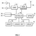
- FIG. 1illustrates a perspective view of an exemplary electronic device within which various embodiments of the present invention may be implemented
- FIG. 2illustrates an exemplary schematic representation of the circuitry which may be included in the electronic device of FIG. 1 .
- FIG. 3illustrates a flow diagram of an exemplary embodiment of the present invention.
- FIG. 4illustrates a flow diagram of another exemplary embodiment of the present invention.
- FIG. 5illustrates an exemplary device in accordance with an embodiment of the present invention.
- a systemmay utilize a mass memory device separate from a system memory device to accommodate different memory access demands.
- the various embodiments of the present inventiondisclose methods, systems and devices to enable run-time configuration of a memory device in accordance with certain memory access profiles.
- the configurationmay be effected for a portion of the memory device, a partition of the memory device, or even one single access location on the memory device. Since the system that accesses the memory device knows, or is capable of determining, the type of memory access needs (e.g., whether it is a read, write, erase, modify attribute, random, or a sequential operation), it can issue commands for configuring the memory device in accordance with an access profile that is most optimized/suitable for the particular access command.
- Such access profilesfor example, may be adapted for optimizing data throughput, lifetime and/or power consumption associated with particular uses of the memory device.
- a default access profilemay be defined to configure a memory device when, for example, the device or system initially boots up.
- Such a default profilewhile providing a starting point for potential future modifications, may be pre-selected to accommodate the most likely access needs for that memory device. This profile may remain in effect until the memory device is powered down, or it may be replaced by another profile in accordance with the embodiments of the present invention.
- the information regarding the nature and type of memory accessallows the memory device to organize itself in a manner that is most suited for a particular access command, resulting in improved performance and higher reliability. These improvements are largely due to the elimination of background operations and unnecessary data merging that are normally associated with traditional memory access methods.
- the techniques of the various embodiments of the present inventionmay be more effective in optimizing sequential memory access operations, where background processing and data merging are more abundant. These optimizations further extend the life of the storage device, and result in reduced energy consumption by the device.
- the embodiments of the present inventionfurther enable the utilization of the same memory device both as the mass storage memory and the system memory, thus eliminating the need for separate memory devices that are utilized in the systems of prior art.
- all non-volatile memory needs of a systemmay be accommodated using a single embedded Multimedia Card (eMMC) memory, where the Operating System image, user data, and other parameters may be stored on the same device.
- eMMCembedded Multimedia Card
- multimedia applicationsthat require very high density mass storage devices (e.g., in the order of several Gigabytes)
- the very same memory devicemay be used to store the various types of user applications, the Operating System and other system data files.
- This consolidationis expected to further spur the adoption of a standardized memory device with higher production volumes, and to eventually lead to lower-cost memory devices.
- the advent of such cost-effective, single-memory devicesare particularly beneficial to the development of mobile devices in which size and cost constraints are most significant.
- a memory device 500may comprise a physical memory 502 with one or more registers 504 for accommodating the predefined access profiles that are used to optimize the memory device.
- the memory device 500may further comprise a receiving means 510 that is adapted to receive one or more commands, through the communication interface 512 , for activating a particular access profile.
- the receiving means 510is illustrated as comprising a separate section of the controller 508 . However, it is understood that the receiving means 510 and the controller 508 may also be implemented as a single entity.
- the controller 508may configure the memory device 500 in accordance with one or more access profiles that reside in memory registers 504 .
- the communication between the controller 508 and the physical memory 502may be conducted through the interface 506 .
- one predefined access profilemay be a burst mode profile that facilitates high-speed transfer of large data chunks and provides a ‘ready’ indication to the host prior to, or after, such transfer.
- the needed flash memory management operationsmay take place subsequent to the transfer at a convenient time, for example, while no other activities or memory access operations are taking place.
- Another example of an access profileincludes a random mode profile which enables quick access to short, random memory locations on the device.
- the memory device in accordance with embodiments of the present inventionmay further comprise another register for accommodating the currently active access profile. This profile, which may be any one of the supported predefined profiles, governs the current access operations to the memory device.
- such registermay comprise a default profile that is activated during the boot up of the host system and/or the power up of the memory device.
- This active profilemay remain in effect until the memory device is powered down, or it may be replaced by another profile in accordance with the embodiments of the present invention.
- Run-time configurability of the memory device in accordance with the present inventionis effected by replacing the contents of the currently active profile register with one of the predefined profiles that resides on the first set of registers. Accordingly, when the need for a new type of memory access arises, a command may be issued to activate a suitable profile. The command may activate any one of the predefined access profiles, including but not limited to, the default profile.
- the various access profilesmay be updated or uploaded onto the memory device.
- an existing access profilemay be augmented (or completely replaced with a new version) to add or remove certain features and functionalities.
- an entirely new access profilemay be uploaded to the memory device, thus increasing the number of available access profiles that can be readily used to configure the memory device.
- an access profilemay be implemented as a binary file that further comprises the required logic to implement an access profile. This way, the access profile may be considered part of the memory device firmware responsible for handling specific accesses needs in an optimized fashion.
- FIGS. 1 and 2show one representative electronic device 12 within which embodiments of the present invention may be implemented. It should be understood, however, that the present invention is not intended to be limited to one particular type of device. In fact, the various embodiments of the present invention may be readily adapted for use in any stand-alone or embedded system that comprises or accesses a memory device.
- 1 and 2includes a housing 30 , a display 32 in the form of a liquid crystal display, a keypad 34 , a microphone 36 , an ear-piece 38 , a battery 40 , an infrared port 42 , an antenna 44 , a smart card 46 in the form of a UICC according to one embodiment, a card reader 48 , radio interface circuitry 52 , codec circuitry 54 , a controller 56 and a memory 58 .
- Individual circuits and elementsare all of a type well known in the art, for example in the Nokia range of mobile telephones.
- FIG. 3is an example flow diagram illustrating run-time configurability of a memory device in accordance to an embodiment of the present invention.
- the memory deviceupon boot up of the system in step 100 , the memory device in accordance with embodiments of the present invention organizes itself according to the default profile in step 102 .
- the exemplary default profile used in FIG. 3configures the memory device to accommodate the reading of large sequential data from the memory device.
- the systemreads a large amount of sequential data, which for example, may comprise the operating system of the host device.
- the systementers an idle state in step 106 .
- the memory devicein step 108 , is commanded to activate an access profile for reading/writing short random data.
- the systemrequires large sequential reads/writes.
- a mass storage devicemay, for example, include a stand-alone memory device such as a USB memory, or a PC or other electronic device that comprises one or more mass storage components.
- the memory devicein accordance with embodiments of the present invention, in step 112 , receives a command to activate the access profile that is optimized for reading/writing large sequential data.
- step 114the system conducts at least a portion of the large sequential read/write transfer. While the large data access operations may be completed without further interruptions, in one exemplary embodiment, the system of the present invention may need to access the memory device in short, random I/O access cycles, as illustrated in step 116 .
- the memory devicemay receive a command to suspend its current access profile, which is directed towards reading/writing long sequential data, and activate an alternate access profile that is optimized for reading/writing short random data.
- the memory devicein step 122 , may receive a subsequent command to revert back to the access profile for reading/writing large sequential data. The system may then resume reading/writing large sequential data in step 124 .
- FIG. 4illustrates an alternate embodiment of the present invention according to which two or more memory access operations (and their corresponding access profiles) may be implemented in parallel.
- steps 200 to 216represent similar operations as their counterparts in FIG. 3 .
- the memory device in accordance with embodiments of the present inventionorganizes itself according to the default profile in step 202 .
- the exemplary default profile used in FIG. 4configures the memory device to accommodate the reading of large sequential data from the memory device.
- step 204the system reads a large amount of sequential data, which for example, may comprise the operating system of the host device.
- the systemUpon completion of the large read operation, the system enters an idle state in step 206 . Since the majority of memory access operations during an idle state is likely to involve short random read/write operations, the memory device, in step 208 , is commanded to activate an access profile for reading/writing short random data. The system may then require access to large sequential reads/writes in step 210 . This need may arise, for example, in preparation for large data transfers to/from an external memory device.
- the memory devicein accordance with embodiments of the present invention, in step 212 , receives a command to activate the access profile that is optimized for reading/writing large sequential data.
- step 214the system conducts at least a portion of the large sequential read/write transfers before the system need for short read/write access cycles to the memory device arises in step 216 .
- the present embodiment in accordance with FIG. 4accommodates both memory access modes by commanding the memory device in accordance with embodiments of the present invention to activate a parallel access profile for reading/writing short random data in step 220 . Accordingly, while the system continues to read/write large sequential data in step 218 , it may simultaneously (or in an interleaved fashion) conduct short memory access operations in step 222 .
- JEDEC eMMCis a standardized mass storage device comprising a memory and a controller device.
- the controllerhandles block-management functions associated with the memory such as logical block allocation and wear leveling.
- the communication between the memory and the host deviceis also handled by the controller according to a standard protocol.
- This protocoldefines, among other signals, a bidirectional command signal, CMD, that is used for device initialization, and transfer of commands between the host and memory device. More specifically, CMD23 (SET_BLOCK_COUNT) defines the number of blocks (read/write) and the reliable writer parameter (write) for a block read/write command. CMD23 includes a 32 bit argument field, of which bits 15 to 0 are allocated for setting the number of blocks for the corresponding read/write command, and bits 30 to 16 are designated as stuff bits. In accordance to one embodiment of the present invention, these stuff bits may be utilized to designate different access profiles for the memory device.
- one profilemay be defined as a burst profile mode, corresponding to a fast, contiguous data access mode.
- the memory deviceimmediately after receiving all the data, may indicate “exit busy” and set the transfer mode to “transfer state,” thus facilitating faster execution of subsequent accesses by the host.
- the memory devicemay also enable the host to send additional commands corresponding to a different access profile. This way, a degree of parallelism in the I/O operations is established.
- access priority levelsmay be defined to resolve access conflicts, where two or more profiles run in parallel and require access to the same memory resource at the same time. Examples of such a memory resources include a RAM buffer, a Flash bus, and other memory resources.
- the access profile associated with a media devicemay be adapted to comprise different control and/or setting profiles that are associated with different partitions of the memory device.
- partitionsmay comprise logical or physical partitions of the memory device. For example, one partition may be configured for random read/write operations while another partition may be configured to provide sequential access.
- a memory access (e.g., an I/O read/write) commandmay be configured to comprise a metadata portion for designating a preferred access profile corresponding to that access command.
- the system in accordance with the present inventionmay recognize that one address is being continuously and frequently updated, and accordingly, it may set an appropriate access profile for that memory command.
- the memory devicedepending on its internal implementations and capabilities—may map such sustained and specific access operations to certain sections of the physical memory with special characteristics. For example, the mapping may be directed to a more a more durable and performance-effective portion of the physical memory, a portion of the memory that utilizes a specific memory technology, or to a separate physical chip that is more suitably designed for such repeated access operations.
- the memory device firmwaremay take an action in accordance with the access profile request of an embodiment of the present invention and handle the I/O operation in a different way.
- the various embodiments of the present inventionare equally applicable to both the embedded memory devices, such as NAND, mass memory, XiP, and similar devices, as well as to removable memory cards.
- a computer-readable mediummay include removable and non-removable storage devices including, but not limited to, Read Only Memory (ROM), Random Access Memory (RAM), compact discs (CDs), digital versatile discs (DVD), etc.
- program modulesmay include routines, programs, objects, components, data structures, etc. that perform particular tasks or implement particular abstract data types.
- Computer-executable instructions, associated data structures, and program modulesrepresent examples of program code for executing steps of the methods disclosed herein. The particular sequence of such executable instructions or associated data structures represents examples of corresponding acts for implementing the functions described in such steps or processes.
Landscapes
- Engineering & Computer Science (AREA)
- Theoretical Computer Science (AREA)
- Physics & Mathematics (AREA)
- General Engineering & Computer Science (AREA)
- General Physics & Mathematics (AREA)
- Human Computer Interaction (AREA)
- Computer Security & Cryptography (AREA)
- Software Systems (AREA)
- Techniques For Improving Reliability Of Storages (AREA)
- Memory System (AREA)
- Information Retrieval, Db Structures And Fs Structures Therefor (AREA)
- Telephone Function (AREA)
- Memory System Of A Hierarchy Structure (AREA)
Abstract
Description
Claims (37)
Priority Applications (26)
| Application Number | Priority Date | Filing Date | Title |
|---|---|---|---|
| US12/039,672US8307180B2 (en) | 2008-02-28 | 2008-02-28 | Extended utilization area for a memory device |
| KR1020137002338AKR101468824B1 (en) | 2008-02-28 | 2009-01-30 | Extended utilization area for a memory device |
| CN200980106241.1ACN101952808B (en) | 2008-02-28 | 2009-01-30 | Extended utilization area for storage devices |
| KR1020107021534AKR101281326B1 (en) | 2008-02-28 | 2009-01-30 | Extended utilization area for a memory device |
| JP2010548134AJP5663720B2 (en) | 2008-02-28 | 2009-01-30 | Extended usage range for memory devices |
| EP18215330.4AEP3493067B1 (en) | 2008-02-28 | 2009-01-30 | Extended utilization area for a memory device |
| EP09715221.9AEP2248023B1 (en) | 2008-02-28 | 2009-01-30 | Extended utilization area for a memory device |
| PCT/FI2009/050083WO2009106680A1 (en) | 2008-02-28 | 2009-01-30 | Extended utilization area for a memory device |
| CN201510093389.3ACN104657284B (en) | 2008-02-28 | 2009-01-30 | Extended utilization area for storage devices |
| US13/645,588US8601228B2 (en) | 2008-02-28 | 2012-10-05 | Extended utilization area for a memory device |
| JP2013103695AJP2013211033A (en) | 2008-02-28 | 2013-05-16 | Expanded utilization range for memory device |
| US13/951,169US9063850B2 (en) | 2008-02-28 | 2013-07-25 | Extended utilization area for a memory device |
| JP2015099731AJP2015164074A (en) | 2008-02-28 | 2015-05-15 | Extended usage range for memory devices |
| US14/732,507US9367486B2 (en) | 2008-02-28 | 2015-06-05 | Extended utilization area for a memory device |
| HK15110890.3AHK1210296B (en) | 2008-02-28 | 2015-11-04 | Extended utilization area for a memory device |
| US15/181,293US10540094B2 (en) | 2008-02-28 | 2016-06-13 | Extended utilization area for a memory device |
| JP2017156699AJP6602823B2 (en) | 2008-02-28 | 2017-08-15 | Extended usage range for memory devices |
| JP2019185570AJP2020074079A (en) | 2008-02-28 | 2019-10-09 | Extended usage range for memory devices |
| US16/598,894US11550476B2 (en) | 2008-02-28 | 2019-10-10 | Extended utilization area for a memory device |
| US16/825,653US11182079B2 (en) | 2008-02-28 | 2020-03-20 | Extended utilization area for a memory device |
| JP2021069406AJP2021108199A (en) | 2008-02-28 | 2021-04-16 | Range of expansion usage for memory apparatus |
| US17/410,588US11494080B2 (en) | 2008-02-28 | 2021-08-24 | Extended utilization area for a memory device |
| US18/045,067US11907538B2 (en) | 2008-02-28 | 2022-10-07 | Extended utilization area for a memory device |
| US18/151,977US11829601B2 (en) | 2008-02-28 | 2023-01-09 | Extended utilization area for a memory device |
| JP2023021268AJP2023055992A (en) | 2008-02-28 | 2023-02-15 | Extended utilization range for memory device |
| US18/520,153US12417022B2 (en) | 2008-02-28 | 2023-11-27 | Extended utilization area for a memory device |
Applications Claiming Priority (1)
| Application Number | Priority Date | Filing Date | Title |
|---|---|---|---|
| US12/039,672US8307180B2 (en) | 2008-02-28 | 2008-02-28 | Extended utilization area for a memory device |
Related Parent Applications (1)
| Application Number | Title | Priority Date | Filing Date |
|---|---|---|---|
| US13/645,588ContinuationUS8601228B2 (en) | 2008-02-28 | 2012-10-05 | Extended utilization area for a memory device |
Related Child Applications (2)
| Application Number | Title | Priority Date | Filing Date |
|---|---|---|---|
| US13/645,588ContinuationUS8601228B2 (en) | 2008-02-28 | 2012-10-05 | Extended utilization area for a memory device |
| US13/951,169ContinuationUS9063850B2 (en) | 2008-02-28 | 2013-07-25 | Extended utilization area for a memory device |
Publications (2)
| Publication Number | Publication Date |
|---|---|
| US20090222639A1 US20090222639A1 (en) | 2009-09-03 |
| US8307180B2true US8307180B2 (en) | 2012-11-06 |
Family
ID=41014077
Family Applications (11)
| Application Number | Title | Priority Date | Filing Date |
|---|---|---|---|
| US12/039,672Active2031-02-22US8307180B2 (en) | 2008-02-28 | 2008-02-28 | Extended utilization area for a memory device |
| US13/645,588ActiveUS8601228B2 (en) | 2008-02-28 | 2012-10-05 | Extended utilization area for a memory device |
| US13/951,169ActiveUS9063850B2 (en) | 2008-02-28 | 2013-07-25 | Extended utilization area for a memory device |
| US14/732,507ActiveUS9367486B2 (en) | 2008-02-28 | 2015-06-05 | Extended utilization area for a memory device |
| US15/181,293ActiveUS10540094B2 (en) | 2008-02-28 | 2016-06-13 | Extended utilization area for a memory device |
| US16/598,894ActiveUS11550476B2 (en) | 2008-02-28 | 2019-10-10 | Extended utilization area for a memory device |
| US16/825,653Active2028-03-16US11182079B2 (en) | 2008-02-28 | 2020-03-20 | Extended utilization area for a memory device |
| US17/410,588ActiveUS11494080B2 (en) | 2008-02-28 | 2021-08-24 | Extended utilization area for a memory device |
| US18/045,067ActiveUS11907538B2 (en) | 2008-02-28 | 2022-10-07 | Extended utilization area for a memory device |
| US18/151,977ActiveUS11829601B2 (en) | 2008-02-28 | 2023-01-09 | Extended utilization area for a memory device |
| US18/520,153ActiveUS12417022B2 (en) | 2008-02-28 | 2023-11-27 | Extended utilization area for a memory device |
Family Applications After (10)
| Application Number | Title | Priority Date | Filing Date |
|---|---|---|---|
| US13/645,588ActiveUS8601228B2 (en) | 2008-02-28 | 2012-10-05 | Extended utilization area for a memory device |
| US13/951,169ActiveUS9063850B2 (en) | 2008-02-28 | 2013-07-25 | Extended utilization area for a memory device |
| US14/732,507ActiveUS9367486B2 (en) | 2008-02-28 | 2015-06-05 | Extended utilization area for a memory device |
| US15/181,293ActiveUS10540094B2 (en) | 2008-02-28 | 2016-06-13 | Extended utilization area for a memory device |
| US16/598,894ActiveUS11550476B2 (en) | 2008-02-28 | 2019-10-10 | Extended utilization area for a memory device |
| US16/825,653Active2028-03-16US11182079B2 (en) | 2008-02-28 | 2020-03-20 | Extended utilization area for a memory device |
| US17/410,588ActiveUS11494080B2 (en) | 2008-02-28 | 2021-08-24 | Extended utilization area for a memory device |
| US18/045,067ActiveUS11907538B2 (en) | 2008-02-28 | 2022-10-07 | Extended utilization area for a memory device |
| US18/151,977ActiveUS11829601B2 (en) | 2008-02-28 | 2023-01-09 | Extended utilization area for a memory device |
| US18/520,153ActiveUS12417022B2 (en) | 2008-02-28 | 2023-11-27 | Extended utilization area for a memory device |
Country Status (6)
| Country | Link |
|---|---|
| US (11) | US8307180B2 (en) |
| EP (2) | EP2248023B1 (en) |
| JP (7) | JP5663720B2 (en) |
| KR (2) | KR101468824B1 (en) |
| CN (2) | CN101952808B (en) |
| WO (1) | WO2009106680A1 (en) |
Cited By (7)
| Publication number | Priority date | Publication date | Assignee | Title |
|---|---|---|---|---|
| US20150160874A1 (en)* | 2012-06-07 | 2015-06-11 | Micron Technology, Inc. | Integrity of an address bus |
| US9311226B2 (en) | 2012-04-20 | 2016-04-12 | Memory Technologies Llc | Managing operational state data of a memory module using host memory in association with state change |
| US10048884B2 (en) | 2011-12-29 | 2018-08-14 | Memory Technologies Llc | Method for erasing data entity in memory module |
| US10101763B2 (en)* | 2015-07-29 | 2018-10-16 | Sandisk Technologies Inc. | Interface adjustment processes for a data storage device |
| US10402106B2 (en) | 2013-12-12 | 2019-09-03 | Memory Technologies Llc | Channel optimized storage modules |
| US10540094B2 (en) | 2008-02-28 | 2020-01-21 | Memory Technologies Llc | Extended utilization area for a memory device |
| US10983697B2 (en) | 2009-06-04 | 2021-04-20 | Memory Technologies Llc | Apparatus and method to share host system RAM with mass storage memory RAM |
Families Citing this family (21)
| Publication number | Priority date | Publication date | Assignee | Title |
|---|---|---|---|---|
| US8307151B1 (en)* | 2009-11-30 | 2012-11-06 | Micron Technology, Inc. | Multi-partitioning feature on e-MMC |
| WO2012065112A2 (en) | 2010-11-12 | 2012-05-18 | Apple Inc. | Apparatus and methods for recordation of device history across multiple software emulations |
| CN102170548A (en)* | 2011-01-28 | 2011-08-31 | 杭州海康威视数字技术股份有限公司 | Mutually exclusive resource remote-access method and digital video recorder |
| US8751728B1 (en) | 2011-04-29 | 2014-06-10 | Western Digital Technologies, Inc. | Storage system bus transfer optimization |
| US9417998B2 (en) | 2012-01-26 | 2016-08-16 | Memory Technologies Llc | Apparatus and method to provide cache move with non-volatile mass memory system |
| US8910017B2 (en) | 2012-07-02 | 2014-12-09 | Sandisk Technologies Inc. | Flash memory with random partition |
| US9519428B2 (en)* | 2012-09-26 | 2016-12-13 | Qualcomm Incorporated | Dynamically improving performance of a host memory controller and a memory device |
| US9569352B2 (en) | 2013-03-14 | 2017-02-14 | Sandisk Technologies Llc | Storage module and method for regulating garbage collection operations based on write activity of a host |
| US9471254B2 (en)* | 2014-04-16 | 2016-10-18 | Sandisk Technologies Llc | Storage module and method for adaptive burst mode |
| US9928169B2 (en) | 2014-05-07 | 2018-03-27 | Sandisk Technologies Llc | Method and system for improving swap performance |
| US9710198B2 (en) | 2014-05-07 | 2017-07-18 | Sandisk Technologies Llc | Method and computing device for controlling bandwidth of swap operations |
| US9665296B2 (en) | 2014-05-07 | 2017-05-30 | Sandisk Technologies Llc | Method and computing device for using both volatile memory and non-volatile swap memory to pre-load a plurality of applications |
| US9633233B2 (en) | 2014-05-07 | 2017-04-25 | Sandisk Technologies Llc | Method and computing device for encrypting data stored in swap memory |
| CN105337944B (en)* | 2014-08-12 | 2020-02-21 | 格马尔托股份有限公司 | Method for managing several profiles in a secure element |
| CN110727399B (en)* | 2015-09-18 | 2021-09-03 | 华为技术有限公司 | Storage array management method and device |
| US9977603B2 (en)* | 2016-05-02 | 2018-05-22 | Micron Technology, Inc. | Memory devices for detecting known initial states and related methods and electronic systems |
| US9990158B2 (en) | 2016-06-22 | 2018-06-05 | Sandisk Technologies Llc | Storage system and method for burst mode management using transfer RAM |
| KR102430983B1 (en) | 2017-09-22 | 2022-08-09 | 삼성전자주식회사 | Storage device and method of operating the same |
| FR3099258B1 (en)* | 2019-07-26 | 2022-06-24 | Idemia Identity & Security France | Dynamic adaptation of a secure element execution environment to profiles |
| US11516431B2 (en) | 2020-07-30 | 2022-11-29 | Microsoft Technology Licensing, Llc | Meeting privacy protection system |
| US11600312B1 (en) | 2021-08-16 | 2023-03-07 | Micron Technology, Inc. | Activate commands for memory preparation |
Citations (13)
| Publication number | Priority date | Publication date | Assignee | Title |
|---|---|---|---|---|
| JPH10228413A (en) | 1997-02-17 | 1998-08-25 | Ge Yokogawa Medical Syst Ltd | Memory access controlling method device therefor and memory system |
| US5809340A (en)* | 1993-04-30 | 1998-09-15 | Packard Bell Nec | Adaptively generating timing signals for access to various memory devices based on stored profiles |
| US6785764B1 (en) | 2000-05-11 | 2004-08-31 | Micron Technology, Inc. | Synchronous flash memory with non-volatile mode register |
| WO2004084231A1 (en) | 2003-03-19 | 2004-09-30 | Koninklijke Philips Electronics N.V. | Universal memory device having a profil storage unit |
| WO2005066773A1 (en) | 2003-12-31 | 2005-07-21 | Sandisk Corporation | Flash memory system startup operation |
| US20050204113A1 (en) | 2004-03-09 | 2005-09-15 | International Business Machines Corp. | Method, system and storage medium for dynamically selecting a page management policy for a memory controller |
| AU2005200855A1 (en) | 2004-02-27 | 2005-09-15 | Orga Systems Gmbh | Device and method for updating the configuration of mobile terminals |
| WO2005088468A2 (en) | 2004-03-10 | 2005-09-22 | Koninklijke Philips Electronics N.V. | Integrated circuit and method for memory access control |
| US20060179212A1 (en) | 2005-02-07 | 2006-08-10 | Kim Jin-Hyuk | Flash memory control devices that support multiple memory mapping schemes and methods of operating same |
| US20060184758A1 (en) | 2005-01-11 | 2006-08-17 | Sony Corporation | Storage device |
| US20060280077A1 (en)* | 2005-06-08 | 2006-12-14 | Fujitsu Limited | Disk recorder |
| US20080080688A1 (en)* | 2006-09-29 | 2008-04-03 | Motorola, Inc. | Method and system for associating a user profile to a caller identifier |
| US20080282030A1 (en) | 2007-05-10 | 2008-11-13 | Dot Hill Systems Corporation | Dynamic input/output optimization within a storage controller |
Family Cites Families (297)
| Publication number | Priority date | Publication date | Assignee | Title |
|---|---|---|---|---|
| US3653001A (en) | 1967-11-13 | 1972-03-28 | Bell Telephone Labor Inc | Time-shared computer graphics system having data processing means at display terminals |
| JPS59135563A (en) | 1983-01-24 | 1984-08-03 | Hitachi Ltd | Computer system with disk/cache device |
| JPS59135563U (en) | 1983-02-28 | 1984-09-10 | ダイセル化学工業株式会社 | optical disc container |
| CA1293819C (en) | 1986-08-29 | 1991-12-31 | Thinking Machines Corporation | Very large scale computer |
| JPS6464073A (en) | 1987-09-03 | 1989-03-09 | Minolta Camera Kk | Image memory |
| JPH0268671A (en)* | 1988-09-02 | 1990-03-08 | Matsushita Electric Ind Co Ltd | image memory |
| JP2804115B2 (en)* | 1988-09-19 | 1998-09-24 | 株式会社日立製作所 | Disk file system |
| JP2661224B2 (en) | 1988-12-23 | 1997-10-08 | 株式会社リコー | Memory expansion method |
| US5781753A (en) | 1989-02-24 | 1998-07-14 | Advanced Micro Devices, Inc. | Semi-autonomous RISC pipelines for overlapped execution of RISC-like instructions within the multiple superscalar execution units of a processor having distributed pipeline control for speculative and out-of-order execution of complex instructions |
| JP3038781B2 (en)* | 1989-04-21 | 2000-05-08 | 日本電気株式会社 | Memory access control circuit |
| JPH0679293B2 (en) | 1990-10-15 | 1994-10-05 | 富士通株式会社 | Computer system |
| US5680570A (en) | 1991-06-12 | 1997-10-21 | Quantum Corporation | Memory system with dynamically allocatable non-volatile storage capability |
| JP3407317B2 (en) | 1991-11-28 | 2003-05-19 | 株式会社日立製作所 | Storage device using flash memory |
| WO1993018461A1 (en) | 1992-03-09 | 1993-09-16 | Auspex Systems, Inc. | High-performance non-volatile ram protected write cache accelerator system |
| JPH06236681A (en)* | 1993-02-12 | 1994-08-23 | Toshiba Corp | Semiconductor memory |
| JPH07105095A (en) | 1993-10-04 | 1995-04-21 | Fuji Electric Co Ltd | Cache control method for disk storage device |
| EP0686971B1 (en) | 1994-06-07 | 2002-02-06 | Hitachi, Ltd. | Information storing device and method for controlling same to record/reproduce information by selecting one of working modes |
| US5710931A (en) | 1994-09-07 | 1998-01-20 | Canon Kabushiki Kaisha | Suspension state control for information processing devices such as battery powered computers |
| JP3687115B2 (en) | 1994-10-27 | 2005-08-24 | ソニー株式会社 | Playback device |
| JPH08161216A (en) | 1994-12-09 | 1996-06-21 | Toshiba Corp | Information processing device with high-speed memory clear function |
| US5586291A (en) | 1994-12-23 | 1996-12-17 | Emc Corporation | Disk controller with volatile and non-volatile cache memories |
| EP0749063A3 (en) | 1995-06-07 | 1999-01-13 | International Business Machines Corporation | Method and apparatus for suspend/resume operation in a computer |
| IT235879Y1 (en) | 1995-06-14 | 2000-07-18 | Olivetti & Co Spa | KEYBOARD FOR DATA INTRODUCTION WITH TRACK POSITIONER |
| US5845313A (en) | 1995-07-31 | 1998-12-01 | Lexar | Direct logical block addressing flash memory mass storage architecture |
| US6393492B1 (en) | 1995-11-03 | 2002-05-21 | Texas Instruments Incorporated | Method and arrangement for operating a mass memory storage peripheral computer device connected to a host computer |
| US5802069A (en) | 1995-11-13 | 1998-09-01 | Intel Corporation | Implementing mass storage device functions using host processor memory |
| US5822553A (en) | 1996-03-13 | 1998-10-13 | Diamond Multimedia Systems, Inc. | Multiple parallel digital data stream channel controller architecture |
| US5838873A (en) | 1996-05-31 | 1998-11-17 | Thomson Consumer Electronics, Inc. | Packetized data formats for digital data storage media |
| US5805882A (en) | 1996-07-19 | 1998-09-08 | Compaq Computer Corporation | Computer system and method for replacing obsolete or corrupt boot code contained within reprogrammable memory with new boot code supplied from an external source through a data port |
| JPH10240607A (en)* | 1997-02-26 | 1998-09-11 | Toshiba Corp | Memory system |
| US5933626A (en) | 1997-06-12 | 1999-08-03 | Advanced Micro Devices, Inc. | Apparatus and method for tracing microprocessor instructions |
| JPH11143643A (en) | 1997-11-06 | 1999-05-28 | Sony Corp | Reproducing device and cache processing method |
| US6226710B1 (en) | 1997-11-14 | 2001-05-01 | Utmc Microelectronic Systems Inc. | Content addressable memory (CAM) engine |
| US5924097A (en) | 1997-12-23 | 1999-07-13 | Unisys Corporation | Balanced input/output task management for use in multiprocessor transaction processing system |
| JP4310821B2 (en) | 1997-12-24 | 2009-08-12 | ソニー株式会社 | Information recording apparatus and method |
| JP3990485B2 (en) | 1997-12-26 | 2007-10-10 | 株式会社ルネサステクノロジ | Semiconductor nonvolatile memory device |
| JPH11259357A (en) | 1998-03-09 | 1999-09-24 | Seiko Epson Corp | Semiconductor integrated device and nonvolatile memory writing method |
| US5999876A (en) | 1998-04-01 | 1999-12-07 | Cummins Engine Company, Inc. | Method and system for communication with an engine control module in sleep mode |
| US6173425B1 (en) | 1998-04-15 | 2001-01-09 | Integrated Device Technology, Inc. | Methods of testing integrated circuits to include data traversal path identification information and related status information in test data streams |
| US6067300A (en) | 1998-06-11 | 2000-05-23 | Cabletron Systems, Inc. | Method and apparatus for optimizing the transfer of data packets between local area networks |
| JP3585091B2 (en)* | 1998-06-15 | 2004-11-04 | 富士通株式会社 | Storage device |
| US6021076A (en) | 1998-07-16 | 2000-02-01 | Rambus Inc | Apparatus and method for thermal regulation in memory subsystems |
| KR100319713B1 (en)* | 1998-07-31 | 2002-04-22 | 윤종용 | Programmable mode register for use in synchronized semiconductor memory device |
| JP2000057039A (en) | 1998-08-03 | 2000-02-25 | Canon Inc | Access control method and device, file system, and information processing device |
| US6721288B1 (en) | 1998-09-16 | 2004-04-13 | Openwave Systems Inc. | Wireless mobile devices having improved operation during network unavailability |
| CA2345123A1 (en) | 1998-09-28 | 2000-04-06 | T Squared G Incorporated | Multibyte random access mass storage/memory system |
| US6279114B1 (en) | 1998-11-04 | 2001-08-21 | Sandisk Corporation | Voltage negotiation in a single host multiple cards system |
| JP2000181784A (en)* | 1998-12-18 | 2000-06-30 | Hitachi Ltd | Rewritable nonvolatile storage device |
| JP2001006379A (en) | 1999-06-16 | 2001-01-12 | Fujitsu Ltd | Flash memory with copy and move functions |
| US7889544B2 (en) | 2004-04-05 | 2011-02-15 | Super Talent Electronics, Inc. | High-speed controller for phase-change memory peripheral device |
| US7702831B2 (en) | 2000-01-06 | 2010-04-20 | Super Talent Electronics, Inc. | Flash memory controller for electronic data flash card |
| US6513094B1 (en) | 1999-08-23 | 2003-01-28 | Advanced Micro Devices, Inc. | ROM/DRAM data bus sharing with write buffer and read prefetch activity |
| JP2001067786A (en)* | 1999-08-30 | 2001-03-16 | Matsushita Electric Ind Co Ltd | Recording and playback device |
| US6757797B1 (en) | 1999-09-30 | 2004-06-29 | Fujitsu Limited | Copying method between logical disks, disk-storage system and its storage medium |
| US6665747B1 (en) | 1999-10-22 | 2003-12-16 | Sun Microsystems, Inc. | Method and apparatus for interfacing with a secondary storage system |
| KR20020050270A (en) | 1999-11-09 | 2002-06-26 | 토토라노 제이. 빈센트 | Dynamically adjusting a processor's operational parameters according to its environment |
| US20060075395A1 (en) | 2004-10-01 | 2006-04-06 | Lee Charles C | Flash card system |
| US7552251B2 (en)* | 2003-12-02 | 2009-06-23 | Super Talent Electronics, Inc. | Single-chip multi-media card/secure digital (MMC/SD) controller reading power-on boot code from integrated flash memory for user storage |
| US6609182B1 (en) | 2000-01-20 | 2003-08-19 | Microsoft Corporation | Smart hibernation on an operating system with page translation |
| JP3955712B2 (en) | 2000-03-03 | 2007-08-08 | 株式会社ルネサステクノロジ | Semiconductor device |
| JP4524439B2 (en)* | 2000-03-30 | 2010-08-18 | ラウンド ロック リサーチ、エルエルシー | Synchronous flash memory with zero latency and zero bus turnaround functions |
| US20020000931A1 (en) | 2000-04-14 | 2002-01-03 | Mark Petronic | User interface for a two-way satellite communication system |
| US6396744B1 (en) | 2000-04-25 | 2002-05-28 | Multi Level Memory Technology | Flash memory with dynamic refresh |
| US6681304B1 (en) | 2000-06-30 | 2004-01-20 | Intel Corporation | Method and device for providing hidden storage in non-volatile memory |
| US6721843B1 (en) | 2000-07-07 | 2004-04-13 | Lexar Media, Inc. | Flash memory architecture implementing simultaneously programmable multiple flash memory banks that are host compatible |
| JP2002023962A (en) | 2000-07-07 | 2002-01-25 | Fujitsu Ltd | Disk device and its controlling method |
| JP3965874B2 (en) | 2000-07-17 | 2007-08-29 | セイコーエプソン株式会社 | Recording method for printing on recording medium using two liquids, recorded matter printed by this recording method, and recording apparatus comprising means for executing this recording method |
| DE10196440B4 (en)* | 2000-07-18 | 2006-03-23 | Intel Corporation, Santa Clara | Control access to multiple isolated storage in an isolated execution environment |
| WO2002026875A1 (en) | 2000-09-25 | 2002-04-04 | Stepan Company | Alkoxylated phosphate esters useful as secondary adhesion promoters, internal mold release agents and viscosity modifiers |
| JP2002108691A (en)* | 2000-09-29 | 2002-04-12 | Mitsubishi Electric Corp | Semiconductor storage device and method of controlling semiconductor storage device |
| US6804763B1 (en) | 2000-10-17 | 2004-10-12 | Igt | High performance battery backed ram interface |
| EP1199723B1 (en)* | 2000-10-18 | 2008-12-31 | STMicroelectronics S.r.l. | Interlaced memory device with random or sequential access |
| US6801994B2 (en)* | 2000-12-20 | 2004-10-05 | Microsoft Corporation | Software management systems and methods for automotive computing devices |
| US6934254B2 (en) | 2001-01-18 | 2005-08-23 | Motorola, Inc. | Method and apparatus for dynamically allocating resources in a communication system |
| US6510488B2 (en)* | 2001-02-05 | 2003-01-21 | M-Systems Flash Disk Pioneers Ltd. | Method for fast wake-up of a flash memory system |
| JP4722305B2 (en)* | 2001-02-27 | 2011-07-13 | 富士通セミコンダクター株式会社 | Memory system |
| US6779045B2 (en) | 2001-03-21 | 2004-08-17 | Intel Corporation | System and apparatus for increasing the number of operations per transmission for a media management system |
| US6883037B2 (en) | 2001-03-21 | 2005-04-19 | Microsoft Corporation | Fast data decoder that operates with reduced output buffer bounds checking |
| US6990571B2 (en) | 2001-04-25 | 2006-01-24 | Intel Corporation | Method for memory optimization in a digital signal processor |
| JP2002351741A (en)* | 2001-05-30 | 2002-12-06 | Matsushita Electric Ind Co Ltd | Semiconductor integrated circuit device |
| US6732221B2 (en) | 2001-06-01 | 2004-05-04 | M-Systems Flash Disk Pioneers Ltd | Wear leveling of static areas in flash memory |
| JP4370063B2 (en) | 2001-06-27 | 2009-11-25 | 富士通マイクロエレクトロニクス株式会社 | Semiconductor memory device control device and semiconductor memory device control method |
| US7668276B2 (en) | 2001-10-22 | 2010-02-23 | Rambus Inc. | Phase adjustment apparatus and method for a memory device signaling system |
| JP2003150445A (en) | 2001-11-13 | 2003-05-23 | Fujitsu Ltd | Computer system having external storage device |
| US6842829B1 (en) | 2001-12-06 | 2005-01-11 | Lsi Logic Corporation | Method and apparatus to manage independent memory systems as a shared volume |
| US6754129B2 (en)* | 2002-01-24 | 2004-06-22 | Micron Technology, Inc. | Memory module with integrated bus termination |
| US7085866B1 (en) | 2002-02-19 | 2006-08-01 | Hobson Richard F | Hierarchical bus structure and memory access protocol for multiprocessor systems |
| FI115562B (en) | 2002-03-27 | 2005-05-31 | Nokia Corp | Method and system for determining power consumption in connection with electronic device and electronic device |
| US6892311B2 (en) | 2002-05-08 | 2005-05-10 | Dell Usa, L.P. | System and method for shutting down a host and storage enclosure if the status of the storage enclosure is in a first condition and is determined that the storage enclosure includes a critical storage volume |
| AU2002304404A1 (en)* | 2002-05-31 | 2003-12-19 | Nokia Corporation | Method and memory adapter for handling data of a mobile device using non-volatile memory |
| JP2004021669A (en) | 2002-06-18 | 2004-01-22 | Sanyo Electric Co Ltd | Transfer control system and transfer controller and recording device and transfer control method |
| JP2004062928A (en) | 2002-07-25 | 2004-02-26 | Hitachi Ltd | Magnetic disk drive and storage system |
| JP4111789B2 (en) | 2002-09-13 | 2008-07-02 | 富士通株式会社 | Semiconductor memory device control method and semiconductor memory device |
| US6901298B1 (en) | 2002-09-30 | 2005-05-31 | Rockwell Automation Technologies, Inc. | Saving and restoring controller state and context in an open operating system |
| US7769893B2 (en) | 2002-10-08 | 2010-08-03 | Koninklijke Philips Electronics N.V. | Integrated circuit and method for establishing transactions |
| US7181611B2 (en) | 2002-10-28 | 2007-02-20 | Sandisk Corporation | Power management block for use in a non-volatile memory system |
| US20040088474A1 (en) | 2002-10-30 | 2004-05-06 | Lin Jin Shin | NAND type flash memory disk device and method for detecting the logical address |
| KR20100072067A (en) | 2002-10-31 | 2010-06-29 | 링 테크노로지 엔터프라이즈, 엘엘씨 | Methods and systems for a storage system |
| US7949777B2 (en) | 2002-11-01 | 2011-05-24 | Avid Technology, Inc. | Communication protocol for controlling transfer of temporal data over a bus between devices in synchronization with a periodic reference signal |
| US7478248B2 (en) | 2002-11-27 | 2009-01-13 | M-Systems Flash Disk Pioneers, Ltd. | Apparatus and method for securing data on a portable storage device |
| US7290093B2 (en) | 2003-01-07 | 2007-10-30 | Intel Corporation | Cache memory to support a processor's power mode of operation |
| US7181574B1 (en) | 2003-01-30 | 2007-02-20 | Veritas Operating Corporation | Server cluster using informed prefetching |
| FI117489B (en) | 2003-02-07 | 2006-10-31 | Nokia Corp | A method for indicating a memory card, a system using a memory card, and a memory card |
| US7233335B2 (en) | 2003-04-21 | 2007-06-19 | Nividia Corporation | System and method for reserving and managing memory spaces in a memory resource |
| US20040230317A1 (en)* | 2003-05-15 | 2004-11-18 | Sun Microsystems, Inc. | Method, system, and program for allocating storage resources |
| TW591372B (en) | 2003-05-15 | 2004-06-11 | High Tech Comp Corp | Power control method of portable electronic device, portable electronic device and electronic system |
| US6981123B2 (en) | 2003-05-22 | 2005-12-27 | Seagate Technology Llc | Device-managed host buffer |
| EP1482412B1 (en) | 2003-05-30 | 2006-08-23 | Agilent Technologies Inc | Shared storage arbitration |
| US7231537B2 (en)* | 2003-07-03 | 2007-06-12 | Micron Technology, Inc. | Fast data access mode in a memory device |
| KR100532448B1 (en) | 2003-07-12 | 2005-11-30 | 삼성전자주식회사 | Memory controller capable of controlling refresh period of memory and method thereof |
| US7822105B2 (en) | 2003-09-02 | 2010-10-26 | Sirf Technology, Inc. | Cross-correlation removal of carrier wave jamming signals |
| US20050071570A1 (en) | 2003-09-26 | 2005-03-31 | Takasugl Robin Alexis | Prefetch controller for controlling retrieval of data from a data storage device |
| US7321958B2 (en) | 2003-10-30 | 2008-01-22 | International Business Machines Corporation | System and method for sharing memory by heterogeneous processors |
| US7120766B2 (en) | 2003-12-22 | 2006-10-10 | Inernational Business Machines Corporation | Apparatus and method to initialize information disposed in an information storage and retrieval system |
| US9298472B2 (en) | 2004-01-27 | 2016-03-29 | Nec Corporation | High-speed restart method, information processing device, and program |
| JP4402997B2 (en) | 2004-03-26 | 2010-01-20 | 株式会社日立製作所 | Storage device |
| EP1870814B1 (en) | 2006-06-19 | 2014-08-13 | Texas Instruments France | Method and apparatus for secure demand paging for processor devices |
| US7152801B2 (en) | 2004-04-16 | 2006-12-26 | Sandisk Corporation | Memory cards having two standard sets of contacts |
| JP2005309653A (en) | 2004-04-20 | 2005-11-04 | Hitachi Global Storage Technologies Netherlands Bv | Disk device and cache control method |
| JP4740234B2 (en) | 2004-04-26 | 2011-08-03 | コーニンクレッカ フィリップス エレクトロニクス エヌ ヴィ | Integrated circuit and transaction transmission method |
| KR20070005730A (en) | 2004-04-28 | 2007-01-10 | 마츠시타 덴끼 산교 가부시키가이샤 | Nonvolatile Memory and Data Recording Method |
| US7480749B1 (en) | 2004-05-27 | 2009-01-20 | Nvidia Corporation | Main memory as extended disk buffer memory |
| US7958292B2 (en) | 2004-06-23 | 2011-06-07 | Marvell World Trade Ltd. | Disk drive system on chip with integrated buffer memory and support for host memory access |
| JP4768237B2 (en) | 2004-06-25 | 2011-09-07 | 株式会社東芝 | Portable electronic device and method for controlling portable electronic device |
| US7380095B2 (en) | 2004-06-30 | 2008-05-27 | Intel Corporation | System and method for simulating real-mode memory access with access to extended memory |
| US7427027B2 (en) | 2004-07-28 | 2008-09-23 | Sandisk Corporation | Optimized non-volatile storage systems |
| US8490102B2 (en)* | 2004-07-29 | 2013-07-16 | International Business Machines Corporation | Resource allocation management using IOC token requestor logic |
| US7233538B1 (en) | 2004-08-02 | 2007-06-19 | Sun Microsystems, Inc. | Variable memory refresh rate for DRAM |
| US8843727B2 (en) | 2004-09-30 | 2014-09-23 | Intel Corporation | Performance enhancement of address translation using translation tables covering large address spaces |
| US7334107B2 (en) | 2004-09-30 | 2008-02-19 | Intel Corporation | Caching support for direct memory access address translation |
| US20060120235A1 (en) | 2004-12-06 | 2006-06-08 | Teac Aerospace Technologies | System and method of erasing non-volatile recording media |
| US20060119602A1 (en) | 2004-12-07 | 2006-06-08 | Fisher Andrew J | Address based graphics protocol |
| US7243173B2 (en) | 2004-12-14 | 2007-07-10 | Rockwell Automation Technologies, Inc. | Low protocol, high speed serial transfer for intra-board or inter-board data communication |
| US7450456B2 (en) | 2005-03-30 | 2008-11-11 | Intel Corporation | Temperature determination and communication for multiple devices of a memory module |
| US7206230B2 (en) | 2005-04-01 | 2007-04-17 | Sandisk Corporation | Use of data latches in cache operations of non-volatile memories |
| KR100626391B1 (en) | 2005-04-01 | 2006-09-20 | 삼성전자주식회사 | OneNand Flash Memory and Data Processing System Including It |
| US7275140B2 (en) | 2005-05-12 | 2007-09-25 | Sandisk Il Ltd. | Flash memory management method that is resistant to data corruption by power loss |
| KR100706246B1 (en) | 2005-05-24 | 2007-04-11 | 삼성전자주식회사 | Memory card can improve read performance |
| US20060288130A1 (en) | 2005-06-21 | 2006-12-21 | Rajesh Madukkarumukumana | Address window support for direct memory access translation |
| US7610445B1 (en) | 2005-07-18 | 2009-10-27 | Palm, Inc. | System and method for improving data integrity and memory performance using non-volatile media |
| US7984084B2 (en) | 2005-08-03 | 2011-07-19 | SanDisk Technologies, Inc. | Non-volatile memory with scheduled reclaim operations |
| US7571295B2 (en)* | 2005-08-04 | 2009-08-04 | Intel Corporation | Memory manager for heterogeneous memory control |
| JP4305429B2 (en) | 2005-08-18 | 2009-07-29 | トヨタ自動車株式会社 | In-wheel suspension |
| JP2007052717A (en) | 2005-08-19 | 2007-03-01 | Fujitsu Ltd | Data transfer apparatus and data transfer method |
| JP4433311B2 (en)* | 2005-09-12 | 2010-03-17 | ソニー株式会社 | Semiconductor memory device, electronic device, and mode setting method |
| JP4685567B2 (en)* | 2005-09-15 | 2011-05-18 | 株式会社日立製作所 | Service providing system by information processing device |
| KR100673013B1 (en)* | 2005-09-21 | 2007-01-24 | 삼성전자주식회사 | Memory controller and data processing system including it |
| US20070079015A1 (en) | 2005-09-30 | 2007-04-05 | Intel Corporation | Methods and arrangements to interface a data storage device |
| CN101278354A (en) | 2005-09-30 | 2008-10-01 | 莫塞德技术公司 | Multiple independent serial link memories |
| JP4903415B2 (en) | 2005-10-18 | 2012-03-28 | 株式会社日立製作所 | Storage control system and storage control method |
| JP2007115382A (en)* | 2005-10-24 | 2007-05-10 | Renesas Technology Corp | Semiconductor integrated circuit, storage device, and control program |
| US7533242B1 (en) | 2005-10-31 | 2009-05-12 | Sun Microsystems, Inc. | Prefetch hardware efficiency via prefetch hint instructions |
| US7783845B2 (en) | 2005-11-14 | 2010-08-24 | Sandisk Corporation | Structures for the management of erase operations in non-volatile memories |
| JP2007156597A (en) | 2005-12-01 | 2007-06-21 | Hitachi Ltd | Storage device |
| US20070136523A1 (en) | 2005-12-08 | 2007-06-14 | Bonella Randy M | Advanced dynamic disk memory module special operations |
| US20070147115A1 (en) | 2005-12-28 | 2007-06-28 | Fong-Long Lin | Unified memory and controller |
| US7492368B1 (en) | 2006-01-24 | 2009-02-17 | Nvidia Corporation | Apparatus, system, and method for coalescing parallel memory requests |
| US20070226795A1 (en) | 2006-02-09 | 2007-09-27 | Texas Instruments Incorporated | Virtual cores and hardware-supported hypervisor integrated circuits, systems, methods and processes of manufacture |
| JP4887824B2 (en)* | 2006-02-16 | 2012-02-29 | 富士通セミコンダクター株式会社 | Memory system |
| US7951008B2 (en) | 2006-03-03 | 2011-05-31 | Igt | Non-volatile memory management technique implemented in a gaming machine |
| JP4167695B2 (en) | 2006-03-28 | 2008-10-15 | 株式会社Snkプレイモア | Game machine |
| US7925860B1 (en) | 2006-05-11 | 2011-04-12 | Nvidia Corporation | Maximized memory throughput using cooperative thread arrays |
| KR101392609B1 (en) | 2006-05-23 | 2014-05-08 | 컨버전트 인텔렉츄얼 프로퍼티 매니지먼트 인코포레이티드 | Apparatus and method for establishing device identifiers for serially interconnected devices |
| US7753281B2 (en)* | 2006-06-01 | 2010-07-13 | Hewlett-Packard Development Company, L.P. | System and method of updating a first version of a data file in a contactless flash memory device |
| JP4182993B2 (en) | 2006-06-30 | 2008-11-19 | Tdk株式会社 | MEMORY CONTROLLER, FLASH MEMORY SYSTEM HAVING MEMORY CONTROLLER, AND FLASH MEMORY CONTROL METHOD |
| JP4749255B2 (en) | 2006-07-03 | 2011-08-17 | 株式会社日立製作所 | Storage system control device having multiple types of storage devices |
| EP2047368A4 (en) | 2006-07-31 | 2009-09-23 | Toshiba Kk | Nonvolatile memory system, and data read/write method for nonvolatile memory system |
| US7676702B2 (en) | 2006-08-14 | 2010-03-09 | International Business Machines Corporation | Preemptive data protection for copy services in storage systems and applications |
| US9798528B2 (en) | 2006-09-13 | 2017-10-24 | International Business Machines Corporation | Software solution for cooperative memory-side and processor-side data prefetching |
| US20080082714A1 (en) | 2006-09-29 | 2008-04-03 | Nasa Hq's. | Systems, methods and apparatus for flash drive |
| US20080081609A1 (en) | 2006-09-29 | 2008-04-03 | Motorola, Inc. | Method and system for associating a user profile to a sim card |
| JP4933211B2 (en) | 2006-10-10 | 2012-05-16 | 株式会社日立製作所 | Storage device, control device, and control method |
| US8935302B2 (en) | 2006-12-06 | 2015-01-13 | Intelligent Intellectual Property Holdings 2 Llc | Apparatus, system, and method for data block usage information synchronization for a non-volatile storage volume |
| TWM317043U (en)* | 2006-12-27 | 2007-08-11 | Genesys Logic Inc | Cache device of the flash memory address transformation layer |
| KR101469512B1 (en) | 2007-01-10 | 2014-12-05 | 모바일 세미컨덕터 코오포레이션 | Adaptive memory system for performance enhancement of external computing devices |
| KR100849182B1 (en) | 2007-01-22 | 2008-07-30 | 삼성전자주식회사 | Semiconductor card package and method of forming the same |
| KR100896181B1 (en)* | 2007-01-26 | 2009-05-12 | 삼성전자주식회사 | Embedded Nand Flash Memory Control Device and Method |
| US8312559B2 (en) | 2007-01-26 | 2012-11-13 | Hewlett-Packard Development Company, L.P. | System and method of wireless security authentication |
| KR100823171B1 (en) | 2007-02-01 | 2008-04-18 | 삼성전자주식회사 | Computer system with partitioned flash translation layer and partitioning method of flash translation layer |
| KR100881052B1 (en) | 2007-02-13 | 2009-01-30 | 삼성전자주식회사 | Mapping Table Search System for Flash Memory and Search Method |
| US8316158B1 (en) | 2007-03-12 | 2012-11-20 | Cypress Semiconductor Corporation | Configuration of programmable device using a DMA controller |
| US20080235477A1 (en) | 2007-03-19 | 2008-09-25 | Rawson Andrew R | Coherent data mover |
| JP2008250961A (en)* | 2007-03-30 | 2008-10-16 | Nec Corp | Storage medium control device, data storage device, data storage system, method and control program |
| JP2008250718A (en) | 2007-03-30 | 2008-10-16 | Toshiba Corp | Storage device using nonvolatile cache memory and control method thereof |
| US7760569B2 (en) | 2007-04-05 | 2010-07-20 | Qimonda Ag | Semiconductor memory device with temperature control |
| KR100855578B1 (en) | 2007-04-30 | 2008-09-01 | 삼성전자주식회사 | Refresh cycle control circuit and refresh cycle control method of semiconductor memory device |
| ATE519320T1 (en) | 2007-05-07 | 2011-08-15 | Vorne Ind Inc | METHOD AND SYSTEM FOR EXPANDING THE CAPACITIES OF IMPLEMENTED DEVICES VIA NETWORK CLIENTS |
| JP2009003783A (en) | 2007-06-22 | 2009-01-08 | Toshiba Corp | Nonvolatile memory control device, control method, and storage device |
| WO2009011052A1 (en) | 2007-07-18 | 2009-01-22 | Fujitsu Limited | Memory refresh device and memory refresh method |
| US8527691B2 (en)* | 2007-07-31 | 2013-09-03 | Panasonic Corporation | Nonvolatile memory device and nonvolatile memory system with fast boot capability |
| US8166238B2 (en) | 2007-10-23 | 2012-04-24 | Samsung Electronics Co., Ltd. | Method, device, and system for preventing refresh starvation in shared memory bank |
| US7730248B2 (en) | 2007-12-13 | 2010-06-01 | Texas Instruments Incorporated | Interrupt morphing and configuration, circuits, systems and processes |
| US8185685B2 (en) | 2007-12-14 | 2012-05-22 | Hitachi Global Storage Technologies Netherlands B.V. | NAND flash module replacement for DRAM module |
| US8880483B2 (en) | 2007-12-21 | 2014-11-04 | Sandisk Technologies Inc. | System and method for implementing extensions to intelligently manage resources of a mass storage system |
| KR101077339B1 (en) | 2007-12-28 | 2011-10-26 | 가부시끼가이샤 도시바 | Semiconductor storage device |
| US8892831B2 (en)* | 2008-01-16 | 2014-11-18 | Apple Inc. | Memory subsystem hibernation |
| US8209463B2 (en)* | 2008-02-05 | 2012-06-26 | Spansion Llc | Expansion slots for flash memory based random access memory subsystem |
| US8332572B2 (en) | 2008-02-05 | 2012-12-11 | Spansion Llc | Wear leveling mechanism using a DRAM buffer |
| US7962684B2 (en) | 2008-02-14 | 2011-06-14 | Sandisk Corporation | Overlay management in a flash memory storage device |
| US8180975B2 (en) | 2008-02-26 | 2012-05-15 | Microsoft Corporation | Controlling interference in shared memory systems using parallelism-aware batch scheduling |
| JP4672742B2 (en)* | 2008-02-27 | 2011-04-20 | 株式会社東芝 | Memory controller and memory system |
| US8307180B2 (en)* | 2008-02-28 | 2012-11-06 | Nokia Corporation | Extended utilization area for a memory device |
| JP4643667B2 (en) | 2008-03-01 | 2011-03-02 | 株式会社東芝 | Memory system |
| US8775718B2 (en) | 2008-05-23 | 2014-07-08 | Netapp, Inc. | Use of RDMA to access non-volatile solid-state memory in a network storage system |
| KR101456976B1 (en) | 2008-06-09 | 2014-11-03 | 삼성전자 주식회사 | Memory test device and testing method for memory |
| US8099522B2 (en) | 2008-06-09 | 2012-01-17 | International Business Machines Corporation | Arrangements for I/O control in a virtualized system |
| US20090313420A1 (en) | 2008-06-13 | 2009-12-17 | Nimrod Wiesz | Method for saving an address map in a memory device |
| US9223642B2 (en) | 2013-03-15 | 2015-12-29 | Super Talent Technology, Corp. | Green NAND device (GND) driver with DRAM data persistence for enhanced flash endurance and performance |
| US8166229B2 (en)* | 2008-06-30 | 2012-04-24 | Intel Corporation | Apparatus and method for multi-level cache utilization |
| US8139430B2 (en) | 2008-07-01 | 2012-03-20 | International Business Machines Corporation | Power-on initialization and test for a cascade interconnect memory system |
| WO2010020992A1 (en) | 2008-08-21 | 2010-02-25 | Xsignnet Ltd. | Storage system and method of operating thereof |
| CN101667103B (en) | 2008-09-01 | 2011-05-04 | 智微科技股份有限公司 | Disk array 5 controller and access method |
| US8103830B2 (en) | 2008-09-30 | 2012-01-24 | Intel Corporation | Disabling cache portions during low voltage operations |
| US8181046B2 (en)* | 2008-10-29 | 2012-05-15 | Sandisk Il Ltd. | Transparent self-hibernation of non-volatile memory system |
| US8316201B2 (en) | 2008-12-18 | 2012-11-20 | Sandisk Il Ltd. | Methods for executing a command to write data from a source location to a destination location in a memory device |
| US8639874B2 (en) | 2008-12-22 | 2014-01-28 | International Business Machines Corporation | Power management of a spare DRAM on a buffered DIMM by issuing a power on/off command to the DRAM device |
| US20100161888A1 (en) | 2008-12-22 | 2010-06-24 | Unity Semiconductor Corporation | Data storage system with non-volatile memory using both page write and block program and block erase |
| US8239613B2 (en) | 2008-12-30 | 2012-08-07 | Intel Corporation | Hybrid memory device |
| US8094500B2 (en) | 2009-01-05 | 2012-01-10 | Sandisk Technologies Inc. | Non-volatile memory and method with write cache partitioning |
| US7830732B2 (en) | 2009-02-11 | 2010-11-09 | Stec, Inc. | Staged-backup flash backed dram module |
| US8832354B2 (en) | 2009-03-25 | 2014-09-09 | Apple Inc. | Use of host system resources by memory controller |
| US8533445B2 (en) | 2009-04-21 | 2013-09-10 | Hewlett-Packard Development Company, L.P. | Disabling a feature that prevents access to persistent secondary storage |
| DE112009004621B4 (en) | 2009-05-04 | 2018-08-23 | Hewlett-Packard Development Company, L.P. | Memory device clear command with a control field controllable by a requester device |
| US8806144B2 (en) | 2009-05-12 | 2014-08-12 | Stec, Inc. | Flash storage device with read cache |
| US8250282B2 (en) | 2009-05-14 | 2012-08-21 | Micron Technology, Inc. | PCM memories for storage bus interfaces |
| US8180981B2 (en)* | 2009-05-15 | 2012-05-15 | Oracle America, Inc. | Cache coherent support for flash in a memory hierarchy |
| US8533437B2 (en) | 2009-06-01 | 2013-09-10 | Via Technologies, Inc. | Guaranteed prefetch instruction |
| US8874824B2 (en) | 2009-06-04 | 2014-10-28 | Memory Technologies, LLC | Apparatus and method to share host system RAM with mass storage memory RAM |
| US20100332922A1 (en) | 2009-06-30 | 2010-12-30 | Mediatek Inc. | Method for managing device and solid state disk drive utilizing the same |
| JP2011022657A (en) | 2009-07-13 | 2011-02-03 | Fujitsu Ltd | Memory system and information processor |
| JP2011028537A (en) | 2009-07-27 | 2011-02-10 | Buffalo Inc | Method to speed up access to external storage device and external storage system |
| US8453021B2 (en) | 2009-07-29 | 2013-05-28 | Stec, Inc. | Wear leveling in solid-state device |
| US8266481B2 (en) | 2009-07-29 | 2012-09-11 | Stec, Inc. | System and method of wear-leveling in flash storage |
| JP5362010B2 (en) | 2009-07-29 | 2013-12-11 | パナソニック株式会社 | Memory device, host device, and memory system |
| JP2011039849A (en) | 2009-08-12 | 2011-02-24 | Canon Inc | Information processing device, control method therefor, and program |
| US8667225B2 (en) | 2009-09-11 | 2014-03-04 | Advanced Micro Devices, Inc. | Store aware prefetching for a datastream |
| US9952977B2 (en) | 2009-09-25 | 2018-04-24 | Nvidia Corporation | Cache operations and policies for a multi-threaded client |
| WO2011044154A1 (en) | 2009-10-05 | 2011-04-14 | Marvell Semiconductor, Inc. | Data caching in non-volatile memory |
| JP2011082911A (en) | 2009-10-09 | 2011-04-21 | Sony Corp | Peripheral device, and device connection system |
| JP5526697B2 (en) | 2009-10-14 | 2014-06-18 | ソニー株式会社 | Storage device and memory system |
| KR101602939B1 (en) | 2009-10-16 | 2016-03-15 | 삼성전자주식회사 | Nonvolatile memory system and method for managing data thereof |
| KR101638061B1 (en) | 2009-10-27 | 2016-07-08 | 삼성전자주식회사 | Flash memory system and flash defrag method thereof |
| US8335897B2 (en) | 2009-12-15 | 2012-12-18 | Seagate Technology Llc | Data storage management in heterogeneous memory systems |
| US8443263B2 (en) | 2009-12-30 | 2013-05-14 | Sandisk Technologies Inc. | Method and controller for performing a copy-back operation |
| US8364886B2 (en) | 2010-01-26 | 2013-01-29 | Seagate Technology Llc | Verifying whether metadata identifies a most current version of stored data in a memory space |
| US8255617B2 (en) | 2010-01-26 | 2012-08-28 | Seagate Technology Llc | Maintaining data integrity in a data storage device |
| US9128718B1 (en) | 2010-03-29 | 2015-09-08 | Amazon Technologies, Inc. | Suspend using internal rewriteable memory |
| US8291172B2 (en) | 2010-04-27 | 2012-10-16 | Via Technologies, Inc. | Multi-modal data prefetcher |
| JP4988007B2 (en) | 2010-05-13 | 2012-08-01 | 株式会社東芝 | Information processing apparatus and driver |
| US8966176B2 (en) | 2010-05-27 | 2015-02-24 | Sandisk Il Ltd. | Memory management storage to a host device |
| KR101734204B1 (en) | 2010-06-01 | 2017-05-12 | 삼성전자주식회사 | Flash memory device and system including program sequencer and program method thereof |
| US8397101B2 (en) | 2010-06-03 | 2013-03-12 | Seagate Technology Llc | Ensuring a most recent version of data is recovered from a memory |
| US8826051B2 (en) | 2010-07-26 | 2014-09-02 | Apple Inc. | Dynamic allocation of power budget to a system having non-volatile memory and a processor |
| CN101916201B (en) | 2010-08-06 | 2015-05-27 | 中兴通讯股份有限公司 | Android-based mobile terminal cold-boot method and device |
| WO2012021380A2 (en) | 2010-08-13 | 2012-02-16 | Rambus Inc. | Fast-wake memory |
| KR101736384B1 (en) | 2010-09-29 | 2017-05-16 | 삼성전자주식회사 | Nonvolatile Memory System |
| US8938574B2 (en) | 2010-10-26 | 2015-01-20 | Lsi Corporation | Methods and systems using solid-state drives as storage controller cache memory |
| KR101691091B1 (en) | 2010-11-08 | 2016-12-30 | 삼성전자주식회사 | Computing system and hibernation method thereof |
| TWI417727B (en) | 2010-11-22 | 2013-12-01 | Phison Electronics Corp | Memory storage device, memory controller thereof, and method for responding instruction sent from host thereof |
| CN103262054B (en) | 2010-12-13 | 2015-11-25 | 桑迪士克科技股份有限公司 | For automatically submitting device, the system and method for storer to |
| GB2486738B (en) | 2010-12-24 | 2018-09-19 | Qualcomm Technologies Int Ltd | Instruction execution |
| US20120179874A1 (en) | 2011-01-07 | 2012-07-12 | International Business Machines Corporation | Scalable cloud storage architecture |
| US20120209413A1 (en) | 2011-02-14 | 2012-08-16 | Microsoft Corporation | Background Audio on Mobile Devices |
| US8694764B2 (en) | 2011-02-24 | 2014-04-08 | Microsoft Corporation | Multi-phase resume from hibernate |
| US8706955B2 (en) | 2011-07-01 | 2014-04-22 | Apple Inc. | Booting a memory device from a host |
| US20130007348A1 (en) | 2011-07-01 | 2013-01-03 | Apple Inc. | Booting Raw Memory from a Host |
| US9645758B2 (en) | 2011-07-22 | 2017-05-09 | Sandisk Technologies Llc | Apparatus, system, and method for indexing data of an append-only, log-based structure |
| US9141394B2 (en) | 2011-07-29 | 2015-09-22 | Marvell World Trade Ltd. | Switching between processor cache and random-access memory |
| JP5762930B2 (en) | 2011-11-17 | 2015-08-12 | 株式会社東芝 | Information processing apparatus and semiconductor memory device |
| TWI521343B (en) | 2011-08-01 | 2016-02-11 | Toshiba Kk | An information processing device, a semiconductor memory device, and a semiconductor memory device |
| CN102511044B (en) | 2011-09-06 | 2013-10-02 | 华为技术有限公司 | A method and device for deleting data |
| US8719464B2 (en) | 2011-11-30 | 2014-05-06 | Advanced Micro Device, Inc. | Efficient memory and resource management |
| US20130145055A1 (en) | 2011-12-02 | 2013-06-06 | Andrew Kegel | Peripheral Memory Management |
| CN103975287B (en) | 2011-12-13 | 2017-04-12 | 英特尔公司 | Enhanced system sleep state support in servers using non-volatile random access memory |
| DE112011105984B4 (en) | 2011-12-20 | 2024-10-17 | Intel Corporation | Dynamic partial shutdown of a memory-side cache in a two-level memory hierarchy |
| CN104011755B (en) | 2011-12-22 | 2018-06-08 | 英特尔公司 | Multi-user electronic wallet and management thereof |
| US9389673B2 (en) | 2011-12-22 | 2016-07-12 | Sandisk Technologies Inc. | Systems and methods of performing a data save operation |
| US9069551B2 (en) | 2011-12-22 | 2015-06-30 | Sandisk Technologies Inc. | Systems and methods of exiting hibernation in response to a triggering event |
| US8879346B2 (en) | 2011-12-30 | 2014-11-04 | Intel Corporation | Mechanisms for enabling power management of embedded dynamic random access memory on a semiconductor integrated circuit package |
| CN102609378B (en) | 2012-01-18 | 2016-03-30 | 中国科学院计算技术研究所 | A kind of message type internal storage access device and access method thereof |
| US9417998B2 (en) | 2012-01-26 | 2016-08-16 | Memory Technologies Llc | Apparatus and method to provide cache move with non-volatile mass memory system |
| US9311226B2 (en) | 2012-04-20 | 2016-04-12 | Memory Technologies Llc | Managing operational state data of a memory module using host memory in association with state change |
| US8930633B2 (en) | 2012-06-14 | 2015-01-06 | International Business Machines Corporation | Reducing read latency using a pool of processing cores |
| US9164804B2 (en) | 2012-06-20 | 2015-10-20 | Memory Technologies Llc | Virtual memory module |
| JP2014044490A (en) | 2012-08-24 | 2014-03-13 | Toshiba Corp | Host device and memory device |
| US9116820B2 (en) | 2012-08-28 | 2015-08-25 | Memory Technologies Llc | Dynamic central cache memory |
| MX364783B (en) | 2012-11-20 | 2019-05-07 | Thstyme Bermuda Ltd | Solid state drive architectures. |
| US9652376B2 (en) | 2013-01-28 | 2017-05-16 | Radian Memory Systems, Inc. | Cooperative flash memory control |
| US9229854B1 (en) | 2013-01-28 | 2016-01-05 | Radian Memory Systems, LLC | Multi-array operation support and related devices, systems and software |
| KR102074329B1 (en) | 2013-09-06 | 2020-02-06 | 삼성전자주식회사 | Storage device and data porcessing method thereof |
| US10248587B2 (en) | 2013-11-08 | 2019-04-02 | Sandisk Technologies Llc | Reduced host data command processing |
| WO2015089230A1 (en) | 2013-12-10 | 2015-06-18 | Memory Technologies Llc | Unified memory type aware storage module |
| US9766823B2 (en) | 2013-12-12 | 2017-09-19 | Memory Technologies Llc | Channel optimized storage modules |
| CN103761988B (en) | 2013-12-27 | 2018-01-16 | 华为技术有限公司 | Solid state hard disc and data movement method |
| US10249351B2 (en) | 2016-11-06 | 2019-04-02 | Intel Corporation | Memory device with flexible internal data write control circuitry |
| KR102765251B1 (en) | 2016-11-16 | 2025-02-07 | 삼성전자주식회사 | Memory device and memory system performing unmap read |
| KR20250135372A (en) | 2024-03-05 | 2025-09-15 | 주식회사 카카오 | Method, server and user terminal for displaying combined content |
- 2008
- 2008-02-28USUS12/039,672patent/US8307180B2/enactiveActive
- 2009
- 2009-01-30EPEP09715221.9Apatent/EP2248023B1/enactiveActive
- 2009-01-30JPJP2010548134Apatent/JP5663720B2/enactiveActive
- 2009-01-30EPEP18215330.4Apatent/EP3493067B1/enactiveActive
- 2009-01-30CNCN200980106241.1Apatent/CN101952808B/enactiveActive
- 2009-01-30KRKR1020137002338Apatent/KR101468824B1/enactiveActive
- 2009-01-30WOPCT/FI2009/050083patent/WO2009106680A1/enactiveApplication Filing
- 2009-01-30CNCN201510093389.3Apatent/CN104657284B/enactiveActive
- 2009-01-30KRKR1020107021534Apatent/KR101281326B1/enactiveActive
- 2012
- 2012-10-05USUS13/645,588patent/US8601228B2/enactiveActive
- 2013
- 2013-05-16JPJP2013103695Apatent/JP2013211033A/enactivePending
- 2013-07-25USUS13/951,169patent/US9063850B2/enactiveActive
- 2015
- 2015-05-15JPJP2015099731Apatent/JP2015164074A/enactivePending
- 2015-06-05USUS14/732,507patent/US9367486B2/enactiveActive
- 2016
- 2016-06-13USUS15/181,293patent/US10540094B2/enactiveActive
- 2017
- 2017-08-15JPJP2017156699Apatent/JP6602823B2/enactiveActive
- 2019
- 2019-10-09JPJP2019185570Apatent/JP2020074079A/enactivePending
- 2019-10-10USUS16/598,894patent/US11550476B2/enactiveActive
- 2020
- 2020-03-20USUS16/825,653patent/US11182079B2/enactiveActive
- 2021
- 2021-04-16JPJP2021069406Apatent/JP2021108199A/enactivePending
- 2021-08-24USUS17/410,588patent/US11494080B2/enactiveActive
- 2022
- 2022-10-07USUS18/045,067patent/US11907538B2/enactiveActive
- 2023
- 2023-01-09USUS18/151,977patent/US11829601B2/enactiveActive
- 2023-02-15JPJP2023021268Apatent/JP2023055992A/enactivePending
- 2023-11-27USUS18/520,153patent/US12417022B2/enactiveActive
Patent Citations (14)
| Publication number | Priority date | Publication date | Assignee | Title |
|---|---|---|---|---|
| US5809340A (en)* | 1993-04-30 | 1998-09-15 | Packard Bell Nec | Adaptively generating timing signals for access to various memory devices based on stored profiles |
| JPH10228413A (en) | 1997-02-17 | 1998-08-25 | Ge Yokogawa Medical Syst Ltd | Memory access controlling method device therefor and memory system |
| US6785764B1 (en) | 2000-05-11 | 2004-08-31 | Micron Technology, Inc. | Synchronous flash memory with non-volatile mode register |
| WO2004084231A1 (en) | 2003-03-19 | 2004-09-30 | Koninklijke Philips Electronics N.V. | Universal memory device having a profil storage unit |
| US20060174056A1 (en) | 2003-03-19 | 2006-08-03 | Koninklijke Philips Electronics N.V. | Universal memory device having a profil storage unit |
| WO2005066773A1 (en) | 2003-12-31 | 2005-07-21 | Sandisk Corporation | Flash memory system startup operation |
| AU2005200855A1 (en) | 2004-02-27 | 2005-09-15 | Orga Systems Gmbh | Device and method for updating the configuration of mobile terminals |
| US20050204113A1 (en) | 2004-03-09 | 2005-09-15 | International Business Machines Corp. | Method, system and storage medium for dynamically selecting a page management policy for a memory controller |
| WO2005088468A2 (en) | 2004-03-10 | 2005-09-22 | Koninklijke Philips Electronics N.V. | Integrated circuit and method for memory access control |
| US20060184758A1 (en) | 2005-01-11 | 2006-08-17 | Sony Corporation | Storage device |
| US20060179212A1 (en) | 2005-02-07 | 2006-08-10 | Kim Jin-Hyuk | Flash memory control devices that support multiple memory mapping schemes and methods of operating same |
| US20060280077A1 (en)* | 2005-06-08 | 2006-12-14 | Fujitsu Limited | Disk recorder |
| US20080080688A1 (en)* | 2006-09-29 | 2008-04-03 | Motorola, Inc. | Method and system for associating a user profile to a caller identifier |
| US20080282030A1 (en) | 2007-05-10 | 2008-11-13 | Dot Hill Systems Corporation | Dynamic input/output optimization within a storage controller |
Non-Patent Citations (6)
| Title |
|---|
| English translation of Office Action for Korean Patent Application No. 10-2010-7021534, dated Sep. 30, 2011. |
| European Search Report for Application No. 09715221.9, dated Oct. 25, 2011. |
| International Search Report for PCT Application No. PCT/FI2009/050083 dated Jun. 3, 2009. |
| Japanese Search Report for corresponding Japanese Patent Application No. 2010-548134 mailed May 10, 2012. |
| JEDEC Standard, "Embedded MultiMediaCard (eMMC) eMMC/Card Product Standard, High Capacity, including Reliable Write, Boot, and Sleep Modes", (MMCA, 4.3), JSED84-A43, (Nov. 2007), (166 pages). |
| Office Action for Korean Patent Application No. 10-2010-7021534, dated Sep. 30, 2011. |
Cited By (25)
| Publication number | Priority date | Publication date | Assignee | Title |
|---|---|---|---|---|
| US11182079B2 (en) | 2008-02-28 | 2021-11-23 | Memory Technologies Llc | Extended utilization area for a memory device |
| US12417022B2 (en) | 2008-02-28 | 2025-09-16 | Memory Technologies Llc | Extended utilization area for a memory device |
| US11907538B2 (en) | 2008-02-28 | 2024-02-20 | Memory Technologies Llc | Extended utilization area for a memory device |
| US11829601B2 (en) | 2008-02-28 | 2023-11-28 | Memory Technologies Llc | Extended utilization area for a memory device |
| US10540094B2 (en) | 2008-02-28 | 2020-01-21 | Memory Technologies Llc | Extended utilization area for a memory device |
| US11550476B2 (en) | 2008-02-28 | 2023-01-10 | Memory Technologies Llc | Extended utilization area for a memory device |
| US11494080B2 (en) | 2008-02-28 | 2022-11-08 | Memory Technologies Llc | Extended utilization area for a memory device |
| US12360670B2 (en) | 2009-06-04 | 2025-07-15 | Memory Technologies Llc | Apparatus and method to share host system RAM with mass storage memory RAM |
| US11775173B2 (en) | 2009-06-04 | 2023-10-03 | Memory Technologies Llc | Apparatus and method to share host system RAM with mass storage memory RAM |
| US11733869B2 (en) | 2009-06-04 | 2023-08-22 | Memory Technologies Llc | Apparatus and method to share host system RAM with mass storage memory RAM |
| US10983697B2 (en) | 2009-06-04 | 2021-04-20 | Memory Technologies Llc | Apparatus and method to share host system RAM with mass storage memory RAM |
| US10048884B2 (en) | 2011-12-29 | 2018-08-14 | Memory Technologies Llc | Method for erasing data entity in memory module |
| US11782647B2 (en) | 2012-04-20 | 2023-10-10 | Memory Technologies Llc | Managing operational state data in memory module |
| US11226771B2 (en) | 2012-04-20 | 2022-01-18 | Memory Technologies Llc | Managing operational state data in memory module |
| US10042586B2 (en) | 2012-04-20 | 2018-08-07 | Memory Technologies Llc | Managing operational state data in memory module |
| US9311226B2 (en) | 2012-04-20 | 2016-04-12 | Memory Technologies Llc | Managing operational state data of a memory module using host memory in association with state change |
| US20150160874A1 (en)* | 2012-06-07 | 2015-06-11 | Micron Technology, Inc. | Integrity of an address bus |
| US9557926B2 (en)* | 2012-06-07 | 2017-01-31 | Micron Technology, Inc. | Integrity of an address bus |
| US11023142B2 (en) | 2013-12-12 | 2021-06-01 | Memory Technologies Llc | Channel optimized storage modules |
| US11016678B2 (en) | 2013-12-12 | 2021-05-25 | Memory Technologies Llc | Channel optimized storage modules |
| US10402106B2 (en) | 2013-12-12 | 2019-09-03 | Memory Technologies Llc | Channel optimized storage modules |
| US11809718B2 (en) | 2013-12-12 | 2023-11-07 | Memory Technologies Llc | Channel optimized storage modules |
| US12353727B2 (en) | 2013-12-12 | 2025-07-08 | Memory Technologies Llc | Channel optimized storage modules |
| US10635131B2 (en)* | 2015-07-29 | 2020-04-28 | Western Digital Technologies, Inc. | Interface adjustment processes for a data storage device |
| US10101763B2 (en)* | 2015-07-29 | 2018-10-16 | Sandisk Technologies Inc. | Interface adjustment processes for a data storage device |
Also Published As
Similar Documents
| Publication | Publication Date | Title |
|---|---|---|
| US12417022B2 (en) | Extended utilization area for a memory device | |
| CN101719103B (en) | Memory device and information processing method based on same | |
| JP2011513823A5 (en) | ||
| HK40009715A (en) | Extended utilization area for a memory device | |
| HK40009715B (en) | Extended utilization area for a memory device | |
| HK1210296B (en) | Extended utilization area for a memory device |
Legal Events
| Date | Code | Title | Description |
|---|---|---|---|
| AS | Assignment | Owner name:NOKIA CORPORATION, FINLAND Free format text:ASSIGNMENT OF ASSIGNORS INTEREST;ASSIGNORS:HYVONEN, JANI;MYLLY, KIMMO;HAKKINEN, JUSSI;AND OTHERS;REEL/FRAME:020937/0331;SIGNING DATES FROM 20080313 TO 20080317 Owner name:NOKIA CORPORATION, FINLAND Free format text:ASSIGNMENT OF ASSIGNORS INTEREST;ASSIGNORS:HYVONEN, JANI;MYLLY, KIMMO;HAKKINEN, JUSSI;AND OTHERS;SIGNING DATES FROM 20080313 TO 20080317;REEL/FRAME:020937/0331 | |
| FEPP | Fee payment procedure | Free format text:PAYOR NUMBER ASSIGNED (ORIGINAL EVENT CODE: ASPN); ENTITY STATUS OF PATENT OWNER: LARGE ENTITY Free format text:PAYER NUMBER DE-ASSIGNED (ORIGINAL EVENT CODE: RMPN); ENTITY STATUS OF PATENT OWNER: LARGE ENTITY | |
| STCF | Information on status: patent grant | Free format text:PATENTED CASE | |
| AS | Assignment | Owner name:MEMORY TECHNOLOGIES LLC, NEVADA Free format text:ASSIGNMENT OF ASSIGNORS INTEREST;ASSIGNOR:NOKIA INC.;REEL/FRAME:030190/0043 Effective date:20130325 Owner name:NOKIA INC., CALIFORNIA Free format text:ASSIGNMENT OF ASSIGNORS INTEREST;ASSIGNOR:NOKIA CORPORATION;REEL/FRAME:030189/0381 Effective date:20130324 | |
| FPAY | Fee payment | Year of fee payment:4 | |
| IPR | Aia trial proceeding filed before the patent and appeal board: inter partes review | Free format text:TRIAL NO: IPR2017-01360 Opponent name:SANDISK LLC, WESTERN DIGITAL CORPORATION, WESTERN Effective date:20170503 | |
| IPR | Aia trial proceeding filed before the patent and appeal board: inter partes review | Free format text:TRIAL NO: IPR2019-00642 Opponent name:KINGSTON TECHNOLOGY COMPANY, INC. Effective date:20190130 | |
| MAFP | Maintenance fee payment | Free format text:PAYMENT OF MAINTENANCE FEE, 8TH YEAR, LARGE ENTITY (ORIGINAL EVENT CODE: M1552); ENTITY STATUS OF PATENT OWNER: LARGE ENTITY Year of fee payment:8 | |
| MAFP | Maintenance fee payment | Free format text:PAYMENT OF MAINTENANCE FEE, 12TH YEAR, LARGE ENTITY (ORIGINAL EVENT CODE: M1553); ENTITY STATUS OF PATENT OWNER: LARGE ENTITY Year of fee payment:12 |