US8305790B2 - Electrical anti-fuse and related applications - Google Patents
Electrical anti-fuse and related applicationsDownload PDFInfo
- Publication number
- US8305790B2 US8305790B2US12/724,556US72455610AUS8305790B2US 8305790 B2US8305790 B2US 8305790B2US 72455610 AUS72455610 AUS 72455610AUS 8305790 B2US8305790 B2US 8305790B2
- Authority
- US
- United States
- Prior art keywords
- transistor
- finfet
- drain
- memory cell
- source
- Prior art date
- Legal status (The legal status is an assumption and is not a legal conclusion. Google has not performed a legal analysis and makes no representation as to the accuracy of the status listed.)
- Expired - Fee Related, expires
Links
Images


Classifications
- H—ELECTRICITY
- H01—ELECTRIC ELEMENTS
- H01L—SEMICONDUCTOR DEVICES NOT COVERED BY CLASS H10
- H01L23/00—Details of semiconductor or other solid state devices
- H01L23/52—Arrangements for conducting electric current within the device in operation from one component to another, i.e. interconnections, e.g. wires, lead frames
- H01L23/522—Arrangements for conducting electric current within the device in operation from one component to another, i.e. interconnections, e.g. wires, lead frames including external interconnections consisting of a multilayer structure of conductive and insulating layers inseparably formed on the semiconductor body
- H01L23/525—Arrangements for conducting electric current within the device in operation from one component to another, i.e. interconnections, e.g. wires, lead frames including external interconnections consisting of a multilayer structure of conductive and insulating layers inseparably formed on the semiconductor body with adaptable interconnections
- H01L23/5252—Arrangements for conducting electric current within the device in operation from one component to another, i.e. interconnections, e.g. wires, lead frames including external interconnections consisting of a multilayer structure of conductive and insulating layers inseparably formed on the semiconductor body with adaptable interconnections comprising anti-fuses, i.e. connections having their state changed from non-conductive to conductive
- G—PHYSICS
- G11—INFORMATION STORAGE
- G11C—STATIC STORES
- G11C17/00—Read-only memories programmable only once; Semi-permanent stores, e.g. manually-replaceable information cards
- G11C17/14—Read-only memories programmable only once; Semi-permanent stores, e.g. manually-replaceable information cards in which contents are determined by selectively establishing, breaking or modifying connecting links by permanently altering the state of coupling elements, e.g. PROM
- G11C17/16—Read-only memories programmable only once; Semi-permanent stores, e.g. manually-replaceable information cards in which contents are determined by selectively establishing, breaking or modifying connecting links by permanently altering the state of coupling elements, e.g. PROM using electrically-fusible links
- H—ELECTRICITY
- H01—ELECTRIC ELEMENTS
- H01L—SEMICONDUCTOR DEVICES NOT COVERED BY CLASS H10
- H01L2924/00—Indexing scheme for arrangements or methods for connecting or disconnecting semiconductor or solid-state bodies as covered by H01L24/00
- H01L2924/0001—Technical content checked by a classifier
- H01L2924/0002—Not covered by any one of groups H01L24/00, H01L24/00 and H01L2224/00
- H—ELECTRICITY
- H01—ELECTRIC ELEMENTS
- H01L—SEMICONDUCTOR DEVICES NOT COVERED BY CLASS H10
- H01L2924/00—Indexing scheme for arrangements or methods for connecting or disconnecting semiconductor or solid-state bodies as covered by H01L24/00
- H01L2924/30—Technical effects
- H01L2924/301—Electrical effects
- H01L2924/3011—Impedance
- H—ELECTRICITY
- H10—SEMICONDUCTOR DEVICES; ELECTRIC SOLID-STATE DEVICES NOT OTHERWISE PROVIDED FOR
- H10B—ELECTRONIC MEMORY DEVICES
- H10B20/00—Read-only memory [ROM] devices
- H—ELECTRICITY
- H10—SEMICONDUCTOR DEVICES; ELECTRIC SOLID-STATE DEVICES NOT OTHERWISE PROVIDED FOR
- H10D—INORGANIC ELECTRIC SEMICONDUCTOR DEVICES
- H10D30/00—Field-effect transistors [FET]
- H10D30/60—Insulated-gate field-effect transistors [IGFET]
- H10D30/62—Fin field-effect transistors [FinFET]
Definitions
- a fuseuses FinFET (Fin Field Effect Transistor) MOS (Metal-Oxide-Silicon) technology and is used in OTP (one-time programmable) memory.
- FinFETFin Field Effect Transistor
- MOSMetal-Oxide-Silicon
- An OTP (one-time programmable) memory in MOSgenerally takes advantages of thin-oxide breakdown, but experiences disadvantages, including unreliability for production. Because the heat generated in a P/N junction can easily be dissipated in a planar structure, spikes in the P/N junction that can be shorted due to dopant migration or inter-diffusion of the contact alloy require an extreme high current, such as an ESD zap, to reliably break the junction. Spikes usually result from a P/N junction being reverse-biased for a long time. An approach tying the gate to the drain and applying a high voltage to the source for using MOS as OTP is also unreliable.
- FIG. 1is a schematic perspective view of an anti-fuse in accordance with some embodiments.
- FIG. 2is a cross section of the anti-fuse of FIG. 1 .
- FIG. 3is a schematic electrical diagram of a memory cell using the anti-fuse of FIG. 1 in accordance with some embodiments.
- FIG. 4is a schematic electrical diagram of a memory cell using the anti-fuse of FIG. 1 in accordance with further embodiments.
- FIG. 5is a schematic electrical diagram of a memory array using the memory cell of FIG. 3 , in accordance with some embodiments.
- Some embodiments disclosed hereinare related to electrical anti-fuses, which can be advantageously used in an OTP memory.
- anti-fuseand “fuse” are used interchangeably in this application.
- a FinFET transistoris used as a (anti-) fuse, and its drain and source are considered two terminals of the fuse.
- the transistorIn normal conditions, the transistor is not operational, its drain and source are not electrically connected. The fuse is therefore open (e.g., its terminals are electrically open).
- the gate of the transistoris then controlled (e.g., to turn off the transistor), and a voltage with appropriate amplitude and duration is applied to the drain of the transistor causing the drain and the source to be electrically shorted. In effect, the two terminals of the fuse are electrically shorted.
- the transistorfunctions as an anti-fuse.
- the fuseis used in an OTP memory array. Other embodiments and related applications are also disclosed.
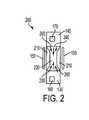
- FIG. 1shows an anti-fuse 100 and FIG. 2 shows a cross section 200 of anti-fuse 100 , in accordance with some embodiments.
- An anti-fuseis a fuse that is normally open (i.e., two terminals of the fuse are open circuit or high impedance). After being programmed, the two terminals of the fuse are electrically shorted allowing a current to flow between the two terminals.
- an “anti-fuse” in this applicationis also referred to as a “fuse.”
- Fuse 100 in FIG. 1is a FinFET transistor.
- fuse 100 or transistor 100are used interchangeably.
- Fuse (or transistor) 100includes a substrate 110 , a fin 120 , a drain 130 , a source 140 , a gate 150 , and two contact regions 160 and 170 .
- transistor 100is symmetrical. That is, a source (e.g., source 140 ) can be selected to be a drain (e.g., drain 130 ) while a drain (e.g., drain 130 ) can be selected to be a source (e.g., source 140 ). Further, drain 130 and source 140 are used as two terminals of fuse 100 .
- gate 150is doped with P implants while drain 130 and source 140 are doped with N+ implants.
- gate 150 , drain 130 , and source 140form two PN junctions 230 and 240 ( FIG. 2 ) including one PN junction 230 from gate 150 to drain 130 and another PN junction 240 from gate 150 to source 140 .
- transistor 100Before being programmed, transistor 100 is off, drain 130 and source 140 are open, the impedance between drain 130 and source 140 is high, and fuse 100 is in the open mode. As a result, there is no current flow between drain 130 and source 140 . After being programmed, drain 130 and source 140 are electrically shorted, fuse 100 is in the closed or shorted mode.
- gate 150 of fuse 100is controlled (e.g., to turn the fuse 100 on or off) and a voltage, e.g., voltage V PROGRAM , having appropriate amplitude and duration is applied to drain 130 .
- transistor 100is off when the voltage at gate 150 to source 140 (V GS of transistor 100 ) is less than a threshold voltage, e.g., voltage V T that turns transistor 100 on.
- V T for transistor 100is about 0.4V. That is, transistor 100 is turned on at about 0.4V.
- transistor 100is off.
- V GSWhen gate 130 is floated or applied with a negative voltage, transistor 100 is also off because V GS is less than V T . If a voltage applied at gate 150 so that V GS is between about 0.1V to 0.3V, transistor 100 is said to have a minor turn-on, a depletion region 210 is generated by this “small” gate voltage, narrows channel 220 and causes drain 130 and source 140 easier to be shorted.
- the amplitude for voltage V PROGRAMis in the range of 1.5-2.0V, and its programming duration is in the range of 50 to 100 microseconds (uS).
- the voltage to control gate 150(to turn if off, to minor turn it on, etc.) varies. Similarly, the amplitude and duration of V PROGRAM also vary.
- gate 150When fuse 100 is being programmed, a current spike occurs under gate 150 and a current flows from drain 130 to source 140 . This is because junction breakdown occurs at junctions 230 and 240 . Excess carriers are induced from drain 130 through channel 220 to source 140 . Because of the high-density current that are induced from drain 130 , the temperature at transistor 100 (e.g., drain 130 , source 140 , channel 220 , etc.), significantly increases. The high temperature and current spike cause oxide breakdown at gate 150 , resulting in drain 130 and source 140 to be electrically shorted. During the process, electrons 260 in contact regions 160 and 170 are removed, and electrons 260 in drain 130 are injected through gate region 150 into source region 140 . In effect, gate region 150 also includes N+ implants causing an N+ channel between drain 130 and source 140 .
- drain 130 and source 140are materialized in FinFET technology because fin 120 is thin, drain 130 and source 140 are small and isolated from substrate 110 such that a very low current can cause a spike, through the thin substrate (or body) region. As fin 120 is thin, the high temperature due to the current spike is retained in fin 120 , enabling a short-circuit between drain 130 and source 140 . This is a reliable and reproducible mechanism for shorting the fuse and thus enabling the use thereof in OTP. For other technologies (e.g., planar technology) without a thin fin, short-circuit between drain 130 and source 140 might not happen because the heat/temperature would dissipate among different parts of transistor 100 .
- planar technologywithout a thin fin
- applying voltage V PROGRAM to drain 130shorts fuse 100 .
- applying voltage V PROGRAM to source 140instead of drain 130 , also shorts fuse 100 .
- FIG. 1shows an NMOS FinFET 100 , but variations and modifications are within the scope of this disclosure.
- a PMOSinstead of an NMOS FinFET is used in some embodiments to create an anti-fuse.
- relevant mechanisms different from those for an NMOSare used, including, for example, connecting the gate of the PMOS FinFET to a positive voltage, to VDD, etc.
- a negative voltage closer to the negative threshold of the PMOS FinFETis used, etc. So that a drain and a source of a PMOS FinFET are shorted, a different voltage level and/or duration is/are used to create the depletion region. This disclosure is not limited to any particular mechanism or technology.
- the source and the drain of the FinFET transistor being used as the fuseare small and isolated from the substrate such that only a very low current can cause a spike through the also thin body region. Further, the thin silicon width can maintain the necessary temperature when a current spike occurs. As a result, mechanisms to short the fuse are reliable and reproducible, and the fuse can advantageously be used in an OTP memory.
- FIG. 3shows a first embodiment of a memory cell 305 for use in a memory array (e.g., array 500 below), in accordance with some embodiments.
- Cell 305includes a fuse 100 connected in series with a FinFET MOS transistor 300 , both of which are shown in circuit representation.
- Transistor 300includes a drain 330 , a source 340 and a gate 350 . Drain 130 is connected to a bit line BL. Source 140 is connected to drain 330 . Gate 350 is connected to a word line WL and source 340 is grounded.
- Transistor 300is also referred to herein as a selector or a selector transistor. When transistor 300 is off, it electrically isolates cell 305 from other components (e.g., of a memory array described below), but when it is on, it enables an electrical path though fuse 100 (e.g., to ground).
- word line WL and bit line BLallows accessing the status or logic level of cell 305 .
- word line WLis selected, which turns on transistor 300 , then bit line BL is sensed (e.g., by a sense amplifier) to detect the impedance of fuse 100 . If this impedance is high, then cell 305 is high. Conversely, if this impedance is low, then cell 305 is low.
- word line WLis selected to turn on transistor 300 .
- Fuse 100is then programmed as discussed above. As fuse 100 is programmed, cell 305 is programmed.
- FIG. 4shows a second embodiment of a memory cell 405 for use in a memory array (e.g., array 500 , below), in accordance with some further embodiments.
- Cell 405also includes a fuse 100 and a selector 300 .
- fuse 100is under (instead of above) selector 300 .
- word line WLwhen word line WL is selected, it turns selector 300 on and creates an electrical path from bit line BL to fuse 100 . Similar to the operation of cell 305 , when selector 300 is turned on, reading BL reveals the status or logic level of memory cell 405 .
- fuse 100is open (e.g., having high impedance) then reading bit line BL reveals the high impedance of fuse 100 . As a result, memory cell 405 is considered as having a high logic. Conversely, if fuse 100 is shorted (e.g., having low impedance) then reading bit line BL reveals the low impedance of fuse 100 , and memory cell 405 is considered as having a low logic.
- word line WLis also selected to turn on selector 300 and thus creates an electrical path from bit line BL to fuse 100 , and fuse 100 is programmed as explained above. Once fuse 100 is programmed, cell 405 is programmed.
- the reading time of memory cell 405is faster than that of cell 305 because selector 300 electrically isolates fuse 100 from other components, and, as a result, effects of parasitic capacitance of fuse 100 can be avoided.
- an NMOS fuse 100 and an NMOS selector 300are shown for illustration only. Variations and modifications are within the spirit and scope of this invention.
- a PMOSinstead of an NMOS transistor, is used as a selector in some embodiments.
- a fuse processed by different technologiese.g., NMOS, PMOS, etc.
- a selector processed by different technologiese.g., NMOS, PMOS, etc.
- This inventionis not limited to any particular combination and/or technology.
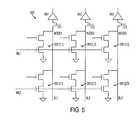
- FIG. 5shows a memory array 500 , in accordance with an embodiment.
- memory array 500includes 2 rows and 3 columns and thus 6 cells 305 , e.g., cells 305 ( 1 , 1 ), 305 ( 1 , 2 ), 305 ( 1 , 3 ), 305 ( 2 , 1 ), 305 ( 2 , 2 ) and 305 ( 2 , 3 ).
- cells 305e.g., cells 305 ( 1 , 1 ), 305 ( 1 , 2 ), 305 ( 1 , 3 ), 305 ( 2 , 1 ), 305 ( 2 , 2 ) and 305 ( 2 , 3 ).
- reference numbers for fuse 100 and transistor 300 and for each gate, drain and source of each fuse 100 and selector transistor 300are not shown.
- Sense amplifiers SA(e.g., SA 1 , SA 2 , SA 3 , etc) in conjunction with transistors TC (e.g., TC 1 , TC 2 , TC 3 ) are used to read the logic level of each cell 305 .
- sense amplifiers SAdetect the impedance at nodes NODE (e.g., NODE 1 , NODE 2 , NODE 3 , etc.) for a corresponding cell 305 . If the impedance is high, then the corresponding cell 305 is high. Conversely, if the impedance is low, then the corresponding cell 305 is low.
- a high at NODE 1indicates that cell 305 ( 1 , 1 ) is high, and a low at NODE 1 indicates that cell 305 ( 1 , 1 ) is low, etc.
- a high at NODE 1indicates that cell 305 ( 2 , 1 ) is high, and a low at NODE 1 indicates that cell 305 ( 2 , 1 ) is low, etc.
- the impedance at a nodeis in effect the impedance of the corresponding fuse 100 for a particular cell 305 .
- the impedance at NODE 1 for cell 305 ( 1 , 1 )is the impedance of fuse 100 ( 1 , 1 ).
- the impedance at NODE 1 for cell 305 ( 2 , 1 )is the impedance of fuse 100 ( 2 , 1 ), etc.
- cell 305 ( 1 , 1 )when cell 305 ( 1 , 1 ) is selected for reading, if fuse 100 ( 1 , 1 ) is high impedance (e.g., fuse 100 ( 1 , 1 ) is open), then cell 305 ( 1 , 1 ) is high, and if fuse 100 ( 1 , 1 ) is low impedance (e.g., fuse 100 ( 1 , 1 ) is shorted), then cell 305 ( 1 , 1 ) is low, etc.
- fuse 100 ( 1 , 1 )is high impedance (e.g., fuse 100 ( 1 , 1 ) is open)
- fuse 100 ( 1 , 1 )is low impedance
- cell 305 ( 1 , 1 )is low, etc.
- a corresponding word line WL and a transistor TCare selected, and a corresponding sense amplifier SA senses the corresponding node.
- a word line WL for a cellis selected (e.g., turns high), it in turn turns on the corresponding selector 300 for that particular cell.
- the corresponding word linee.g., word line WL 1
- transistor TC 1is also turned on.
- Sense amplifier SA 1then senses the impedance at NODE 1 .
- NODE 1If NODE 1 is high then cell 305 ( 1 , 1 ) is high, and if NODE 1 is low then cell 305 ( 1 , 1 ) is low. Similarly, to read cell 305 ( 1 , 2 ), word line WL 1 is selected, which turns on selector 300 ( 1 , 2 ). Further, transistor TC 2 is also turned on. Sense amplifier SA 2 then senses the impedance at NODE 2 . If NODE 2 is high then cell 300 ( 1 , 2 ) is high, and if NODE 2 is low then cell 305 ( 1 , 2 ) is low, etc.
- a corresponding word line WLis selected, and fuse 100 corresponding to that cell 305 is programmed as discussed above.
- transistor 100is turned off, and a voltage (e.g., V PROGRAM ) having appropriate amplitude and period is applied at the corresponding bit line BL.
- V PROGRAMvoltage
- a currentflows from the corresponding BL through the drain 130 and shorts the drain 130 and source 140 of that transistor 100 .
- fuse (or transistor) 100is programmed, the corresponding cell 305 is programmed.
- word line WL 1is selected, which turns on transistor 300 ( 1 , 1 ).
- Fuse (or transistor) 100 ( 1 , 1 )is turned off by having gate 150 floated or applied with a voltage less the threshold voltage V T .
- Voltage V PROGRAM having an amplitude of 1.5-2V and a period of between 50-100 uSis then applied at bit line BL 1 , which will cause a current to flow from bit line BL 1 through the drain 130 of fuse 100 ( 1 , 1 ) and shorts drain 130 and source 140 of fuse 100 ( 1 , 1 ).
- word lines WLmay be referred to as X-decoders while bit lines BL may be referred to as Y-decoders.
- memory array 500is shown to have 6 cells for illustration only, other embodiments include memory arrays having different configurations with different numbers of cells, rows and columns, and the operation of such memory arrays is apparent to a person of ordinary skill in the art from the above examples. Additionally, variations of cells 305 and 405 are used in memory arrays in accordance with one or more embodiments. The instant disclosure is not limited to any particular configuration or variation of a memory cell/array.
Landscapes
- Physics & Mathematics (AREA)
- Condensed Matter Physics & Semiconductors (AREA)
- General Physics & Mathematics (AREA)
- Engineering & Computer Science (AREA)
- Computer Hardware Design (AREA)
- Microelectronics & Electronic Packaging (AREA)
- Power Engineering (AREA)
- Read Only Memory (AREA)
Abstract
Description
Claims (23)
Priority Applications (4)
| Application Number | Priority Date | Filing Date | Title |
|---|---|---|---|
| US12/724,556US8305790B2 (en) | 2009-03-16 | 2010-03-16 | Electrical anti-fuse and related applications |
| US12/766,233US9484462B2 (en) | 2009-09-24 | 2010-04-23 | Fin structure of fin field effect transistor |
| US14/102,702US9660082B2 (en) | 2009-07-28 | 2013-12-11 | Integrated circuit transistor structure with high germanium concentration SiGe stressor |
| US15/339,258US10355108B2 (en) | 2009-09-24 | 2016-10-31 | Method of forming a fin field effect transistor comprising two etching steps to define a fin structure |
Applications Claiming Priority (2)
| Application Number | Priority Date | Filing Date | Title |
|---|---|---|---|
| US16049409P | 2009-03-16 | 2009-03-16 | |
| US12/724,556US8305790B2 (en) | 2009-03-16 | 2010-03-16 | Electrical anti-fuse and related applications |
Publications (2)
| Publication Number | Publication Date |
|---|---|
| US20100232203A1 US20100232203A1 (en) | 2010-09-16 |
| US8305790B2true US8305790B2 (en) | 2012-11-06 |
Family
ID=42730579
Family Applications (1)
| Application Number | Title | Priority Date | Filing Date |
|---|---|---|---|
| US12/724,556Expired - Fee RelatedUS8305790B2 (en) | 2009-03-16 | 2010-03-16 | Electrical anti-fuse and related applications |
Country Status (1)
| Country | Link |
|---|---|
| US (1) | US8305790B2 (en) |
Cited By (4)
| Publication number | Priority date | Publication date | Assignee | Title |
|---|---|---|---|---|
| US20150187431A1 (en)* | 2010-08-20 | 2015-07-02 | Shine C. Chung | ONE-TIME PROGRAMMABLE MEMORY DEVICES USING FinFET TECHNOLOGY |
| US9355740B2 (en) | 2014-03-12 | 2016-05-31 | Kabushiki Kaisha Toshiba | Semiconductor nonvolatile memory device with one-time programmable memories |
| US9502425B2 (en) | 2013-11-04 | 2016-11-22 | Samsung Electronics Co., Ltd. | Semiconductor device and method of manufacturing the same |
| US12414293B2 (en) | 2023-03-20 | 2025-09-09 | Ememory Technology Inc. | Antifuse-type one time programming memory with forksheet transistors |
Families Citing this family (60)
| Publication number | Priority date | Publication date | Assignee | Title |
|---|---|---|---|---|
| US9224496B2 (en) | 2010-08-11 | 2015-12-29 | Shine C. Chung | Circuit and system of aggregated area anti-fuse in CMOS processes |
| US10249379B2 (en) | 2010-08-20 | 2019-04-02 | Attopsemi Technology Co., Ltd | One-time programmable devices having program selector for electrical fuses with extended area |
| US8488359B2 (en) | 2010-08-20 | 2013-07-16 | Shine C. Chung | Circuit and system of using junction diode as program selector for one-time programmable devices |
| US9019742B2 (en) | 2010-08-20 | 2015-04-28 | Shine C. Chung | Multiple-state one-time programmable (OTP) memory to function as multi-time programmable (MTP) memory |
| US9496033B2 (en) | 2010-08-20 | 2016-11-15 | Attopsemi Technology Co., Ltd | Method and system of programmable resistive devices with read capability using a low supply voltage |
| US9042153B2 (en) | 2010-08-20 | 2015-05-26 | Shine C. Chung | Programmable resistive memory unit with multiple cells to improve yield and reliability |
| US10229746B2 (en) | 2010-08-20 | 2019-03-12 | Attopsemi Technology Co., Ltd | OTP memory with high data security |
| US9818478B2 (en) | 2012-12-07 | 2017-11-14 | Attopsemi Technology Co., Ltd | Programmable resistive device and memory using diode as selector |
| US9025357B2 (en) | 2010-08-20 | 2015-05-05 | Shine C. Chung | Programmable resistive memory unit with data and reference cells |
| US9236141B2 (en) | 2010-08-20 | 2016-01-12 | Shine C. Chung | Circuit and system of using junction diode of MOS as program selector for programmable resistive devices |
| US9251893B2 (en) | 2010-08-20 | 2016-02-02 | Shine C. Chung | Multiple-bit programmable resistive memory using diode as program selector |
| US10916317B2 (en) | 2010-08-20 | 2021-02-09 | Attopsemi Technology Co., Ltd | Programmable resistance memory on thin film transistor technology |
| US8830720B2 (en) | 2010-08-20 | 2014-09-09 | Shine C. Chung | Circuit and system of using junction diode as program selector and MOS as read selector for one-time programmable devices |
| US9070437B2 (en) | 2010-08-20 | 2015-06-30 | Shine C. Chung | Circuit and system of using junction diode as program selector for one-time programmable devices with heat sink |
| US8804398B2 (en) | 2010-08-20 | 2014-08-12 | Shine C. Chung | Reversible resistive memory using diodes formed in CMOS processes as program selectors |
| US9711237B2 (en) | 2010-08-20 | 2017-07-18 | Attopsemi Technology Co., Ltd. | Method and structure for reliable electrical fuse programming |
| US9824768B2 (en) | 2015-03-22 | 2017-11-21 | Attopsemi Technology Co., Ltd | Integrated OTP memory for providing MTP memory |
| US9431127B2 (en) | 2010-08-20 | 2016-08-30 | Shine C. Chung | Circuit and system of using junction diode as program selector for metal fuses for one-time programmable devices |
| US8488364B2 (en) | 2010-08-20 | 2013-07-16 | Shine C. Chung | Circuit and system of using a polysilicon diode as program selector for resistive devices in CMOS logic processes |
| US10923204B2 (en) | 2010-08-20 | 2021-02-16 | Attopsemi Technology Co., Ltd | Fully testible OTP memory |
| US9019791B2 (en) | 2010-11-03 | 2015-04-28 | Shine C. Chung | Low-pin-count non-volatile memory interface for 3D IC |
| US8913449B2 (en) | 2012-03-11 | 2014-12-16 | Shine C. Chung | System and method of in-system repairs or configurations for memories |
| US9076513B2 (en) | 2010-11-03 | 2015-07-07 | Shine C. Chung | Low-pin-count non-volatile memory interface with soft programming capability |
| US8988965B2 (en) | 2010-11-03 | 2015-03-24 | Shine C. Chung | Low-pin-count non-volatile memory interface |
| US9496265B2 (en) | 2010-12-08 | 2016-11-15 | Attopsemi Technology Co., Ltd | Circuit and system of a high density anti-fuse |
| US10586832B2 (en) | 2011-02-14 | 2020-03-10 | Attopsemi Technology Co., Ltd | One-time programmable devices using gate-all-around structures |
| US10192615B2 (en) | 2011-02-14 | 2019-01-29 | Attopsemi Technology Co., Ltd | One-time programmable devices having a semiconductor fin structure with a divided active region |
| US8848423B2 (en) | 2011-02-14 | 2014-09-30 | Shine C. Chung | Circuit and system of using FinFET for building programmable resistive devices |
| US8607019B2 (en) | 2011-02-15 | 2013-12-10 | Shine C. Chung | Circuit and method of a memory compiler based on subtractive approach |
| US8570811B2 (en)* | 2011-08-26 | 2013-10-29 | Broadcom Corporation | FinFET based one-time programmable device and related method |
| US9324849B2 (en) | 2011-11-15 | 2016-04-26 | Shine C. Chung | Structures and techniques for using semiconductor body to construct SCR, DIAC, or TRIAC |
| US8912576B2 (en) | 2011-11-15 | 2014-12-16 | Shine C. Chung | Structures and techniques for using semiconductor body to construct bipolar junction transistors |
| US9136261B2 (en) | 2011-11-15 | 2015-09-15 | Shine C. Chung | Structures and techniques for using mesh-structure diodes for electro-static discharge (ESD) protection |
| US8742457B2 (en) | 2011-12-16 | 2014-06-03 | Taiwan Semiconductor Manufacturing Company, Ltd. | Anti-fuses on semiconductor fins |
| US8917533B2 (en) | 2012-02-06 | 2014-12-23 | Shine C. Chung | Circuit and system for testing a one-time programmable (OTP) memory |
| US9007804B2 (en) | 2012-02-06 | 2015-04-14 | Shine C. Chung | Circuit and system of protective mechanisms for programmable resistive memories |
| US8861249B2 (en) | 2012-02-06 | 2014-10-14 | Shine C. Chung | Circuit and system of a low density one-time programmable memory |
| FR2993389B1 (en)* | 2012-07-10 | 2015-02-27 | Soitec Silicon On Insulator | antifuse |
| US9536883B2 (en)* | 2012-07-12 | 2017-01-03 | Broadcom Corporation | Dual anti-fuse |
| US9076526B2 (en) | 2012-09-10 | 2015-07-07 | Shine C. Chung | OTP memories functioning as an MTP memory |
| US9183897B2 (en) | 2012-09-30 | 2015-11-10 | Shine C. Chung | Circuits and methods of a self-timed high speed SRAM |
| US9324447B2 (en) | 2012-11-20 | 2016-04-26 | Shine C. Chung | Circuit and system for concurrently programming multiple bits of OTP memory devices |
| JP2015142175A (en)* | 2014-01-27 | 2015-08-03 | 株式会社東芝 | Programmable logic circuit and nonvolatile fpga |
| US9412473B2 (en) | 2014-06-16 | 2016-08-09 | Shine C. Chung | System and method of a novel redundancy scheme for OTP |
| US10038000B2 (en)* | 2015-09-17 | 2018-07-31 | Taiwan Semiconductor Manufacturing Co., Ltd. | Memory cell and fabricating method thereof |
| US10109364B2 (en)* | 2015-10-21 | 2018-10-23 | Avago Technologies General Ip (Singapore) Pte. Ltd. | Non-volatile memory cell having multiple signal pathways to provide access to an antifuse of the memory cell |
| US10014066B2 (en) | 2015-11-30 | 2018-07-03 | Taiwan Semiconductor Manufacturing Company, Ltd. | Anti-fuse cell structure including reading and programming devices with different gate dielectric thickness |
| US9773792B1 (en) | 2016-03-25 | 2017-09-26 | Taiwan Semiconductor Manufacturing Co., Ltd. | One-time programming cell |
| US10090027B2 (en) | 2016-05-25 | 2018-10-02 | Ememory Technology Inc. | Memory system with low read power |
| US10535413B2 (en) | 2017-04-14 | 2020-01-14 | Attopsemi Technology Co., Ltd | Low power read operation for programmable resistive memories |
| US11062786B2 (en) | 2017-04-14 | 2021-07-13 | Attopsemi Technology Co., Ltd | One-time programmable memories with low power read operation and novel sensing scheme |
| US11615859B2 (en) | 2017-04-14 | 2023-03-28 | Attopsemi Technology Co., Ltd | One-time programmable memories with ultra-low power read operation and novel sensing scheme |
| US10726914B2 (en) | 2017-04-14 | 2020-07-28 | Attopsemi Technology Co. Ltd | Programmable resistive memories with low power read operation and novel sensing scheme |
| EP3407383B1 (en)* | 2017-05-25 | 2020-11-18 | eMemory Technology Inc. | Non-volatile memory and method for programming and reading a memory array having the same |
| US10770160B2 (en) | 2017-11-30 | 2020-09-08 | Attopsemi Technology Co., Ltd | Programmable resistive memory formed by bit slices from a standard cell library |
| US10763269B2 (en) | 2018-10-28 | 2020-09-01 | Taiwan Semiconductor Manufacturing Co., Ltd. | Anti-fuse cell and chip having anti-fuse cells |
| US11404370B2 (en)* | 2019-11-27 | 2022-08-02 | Infineon Technologies Ag | Failure structure in semiconductor device |
| US11276469B2 (en)* | 2020-06-15 | 2022-03-15 | Taiwan Semiconductor Manufacturing Company, Ltd. | One time programmable memory |
| US11758714B2 (en) | 2020-07-31 | 2023-09-12 | Taiwan Semiconductor Manufacturing Co., Ltd. | Fuse cell structure |
| US11930636B2 (en)* | 2021-09-07 | 2024-03-12 | Micron Technology, Inc. | Transistor antifuse, and related devices, systems, and methods |
Citations (142)
| Publication number | Priority date | Publication date | Assignee | Title |
|---|---|---|---|---|
| US5581202A (en) | 1993-11-08 | 1996-12-03 | Hitachi, Ltd. | Semiconductor integrated circuit device and production method thereof |
| US5658417A (en) | 1992-12-08 | 1997-08-19 | Nec Corporation | HF vapor selective etching method and apparatus |
| US5767732A (en) | 1995-06-26 | 1998-06-16 | Samsung Electronics Co., Ltd. | Circuit for permanently adjusting a circuit element value in a semiconductor integrated circuit using fuse elements |
| US5963789A (en) | 1996-07-08 | 1999-10-05 | Kabushiki Kaisha Toshiba | Method for silicon island formation |
| US6065481A (en) | 1997-03-26 | 2000-05-23 | Fsi International, Inc. | Direct vapor delivery of enabling chemical for enhanced HF etch process performance |
| US6121786A (en) | 1997-06-30 | 2000-09-19 | Matsushita Electric Industrial Co., Ltd. | Semiconductor integrated circuit |
| US6503794B1 (en) | 1997-04-10 | 2003-01-07 | Hitachi, Ltd. | Semiconductor integrated circuit device and method for manufacturing the same |
| US20030080361A1 (en) | 2001-11-01 | 2003-05-01 | Anand Murthy | Semiconductor transistor having a stressed channel |
| US6613634B2 (en) | 2000-08-15 | 2003-09-02 | Hitachi, Ltd. | Method of manufacturing a semiconductor device using oblique ion injection |
| US6622738B2 (en) | 2000-10-16 | 2003-09-23 | Micron Technology, Inc. | Apparatus and system for removing photoresist through the use of hot deionized water bath, water vapor and ozone gas |
| US6642090B1 (en) | 2002-06-03 | 2003-11-04 | International Business Machines Corporation | Fin FET devices from bulk semiconductor and method for forming |
| US20030234422A1 (en) | 2002-06-20 | 2003-12-25 | Micron Technology, Inc. | Methods of fabricating a dielectric plug in mosfets to suppress short-channel effects |
| US6706571B1 (en) | 2002-10-22 | 2004-03-16 | Advanced Micro Devices, Inc. | Method for forming multiple structures in a semiconductor device |
| US6727557B2 (en) | 2001-12-07 | 2004-04-27 | Fujitsu Limited | Semiconductor device having well tap provided in memory cell |
| US6740247B1 (en) | 1999-02-05 | 2004-05-25 | Massachusetts Institute Of Technology | HF vapor phase wafer cleaning and oxide etching |
| US6762448B1 (en) | 2003-04-03 | 2004-07-13 | Advanced Micro Devices, Inc. | FinFET device with multiple fin structures |
| US20040192067A1 (en) | 2003-02-28 | 2004-09-30 | Bruno Ghyselen | Method for forming a relaxed or pseudo-relaxed useful layer on a substrate |
| US6828646B2 (en) | 2001-10-17 | 2004-12-07 | Stmicroelectronics Sa | Isolating trench and manufacturing process |
| US6830994B2 (en) | 2001-03-09 | 2004-12-14 | Semiconductor Energy Laboratory Co., Ltd. | Method of manufacturing a semiconductor device having a crystallized semiconductor film |
| US20040259315A1 (en) | 2003-06-09 | 2004-12-23 | Canon Kabushiki Kaisha | Semiconductor substrate, semiconductor device, and method of manufacturing the same |
| US20050020020A1 (en) | 2002-07-16 | 2005-01-27 | Nadine Collaert | Integrated semiconductor fin device and a method for manufacturing such device |
| US6858478B2 (en) | 2002-08-23 | 2005-02-22 | Intel Corporation | Tri-gate devices and methods of fabrication |
| US6872647B1 (en) | 2003-05-06 | 2005-03-29 | Advanced Micro Devices, Inc. | Method for forming multiple fins in a semiconductor device |
| US20050082616A1 (en) | 2003-10-20 | 2005-04-21 | Huajie Chen | High performance stress-enhanced MOSFETs using Si:C and SiGe epitaxial source/drain and method of manufacture |
| US20050153490A1 (en) | 2003-12-16 | 2005-07-14 | Jae-Man Yoon | Method of forming fin field effect transistor |
| US20050170593A1 (en) | 2004-02-02 | 2005-08-04 | Hee-Soo Kang | Method for forming a FinFET by a damascene process |
| US6940747B1 (en) | 2004-05-26 | 2005-09-06 | Hewlett-Packard Development Company, L.P. | Magnetic memory device |
| US6949768B1 (en) | 2004-10-18 | 2005-09-27 | International Business Machines Corporation | Planar substrate devices integrated with finfets and method of manufacture |
| US20050212080A1 (en) | 2004-03-23 | 2005-09-29 | Shien-Yang Wu | Diode junction poly fuse |
| US20050221591A1 (en) | 2004-04-06 | 2005-10-06 | International Business Machines Corporation | Method of forming high-quality relaxed SiGe alloy layers on bulk Si substrates |
| US20050224800A1 (en) | 2004-03-31 | 2005-10-13 | Nick Lindert | Bulk non-planar transistor having strained enhanced mobility and methods of fabrication |
| US6964832B2 (en) | 2002-06-06 | 2005-11-15 | Hitachi, Ltd. | Semiconductor device and manufacturing method thereof |
| US20050266698A1 (en) | 2004-05-26 | 2005-12-01 | International Business Machines Corporation | Exposed pore sealing post patterning |
| US20050280102A1 (en) | 2004-06-16 | 2005-12-22 | Chang-Woo Oh | Field effect transistor and method for manufacturing the same |
| US20060038230A1 (en) | 2004-08-20 | 2006-02-23 | Samsung Electronics Co., Ltd. | Transistor and method of manufacturing the same |
| US7009273B2 (en) | 2002-09-19 | 2006-03-07 | Kabushiki Kaisha Toshiba | Semiconductor device with a cavity therein and a method of manufacturing the same |
| US7018901B1 (en) | 2004-09-29 | 2006-03-28 | Freescale Semiconductor, Inc. | Method for forming a semiconductor device having a strained channel and a heterojunction source/drain |
| US7026232B1 (en) | 2004-12-23 | 2006-04-11 | Texas Instruments Incorporated | Systems and methods for low leakage strained-channel transistor |
| US20060091937A1 (en) | 2004-11-04 | 2006-05-04 | Hynix Semiconductor Inc. | Internal voltage generator |
| US20060105557A1 (en) | 2004-11-12 | 2006-05-18 | Veit Klee | Method of making fully silicided gate electrode |
| US20060128071A1 (en)* | 2002-12-20 | 2006-06-15 | Rankin Jed H | Integrated antifuse structure for finfet and cmos devices |
| US7067400B2 (en) | 2004-09-17 | 2006-06-27 | International Business Machines Corporation | Method for preventing sidewall consumption during oxidation of SGOI islands |
| US20060138572A1 (en) | 2003-08-29 | 2006-06-29 | Kabushiki Kaisha Toshiba | Semiconductor device and method for manufacturing the same |
| US20060151808A1 (en) | 2005-01-12 | 2006-07-13 | Chien-Hao Chen | MOSFET device with localized stressor |
| US20060166475A1 (en) | 2003-03-10 | 2006-07-27 | Siegfried Mantl | Method for the production of stree-relaxed layer structure on a non-lattice adapted substrate and utilization of said layer system in electronic and/or optoelectronic components |
| US7084079B2 (en) | 2001-08-10 | 2006-08-01 | International Business Machines Corporation | Method for low temperature chemical vapor deposition of low-k films using selected cyclosiloxane and ozone gases for semiconductor applications |
| US7084506B2 (en) | 2004-05-13 | 2006-08-01 | Fujitsu Limited | Semiconductor device |
| US7112495B2 (en) | 2003-08-15 | 2006-09-26 | Taiwan Semiconductor Manufacturing Company, Ltd. | Structure and method of a strained channel transistor and a second semiconductor component in an integrated circuit |
| US20060214212A1 (en) | 2005-03-23 | 2006-09-28 | Renesas Technology Corp. | Semiconductor device and method of manufacturing semiconductor device |
| US20060258156A1 (en) | 2005-05-16 | 2006-11-16 | Interuniversitair Microelektronica Centrum (Imec) | Method for forming fully silicided gates and devices obtained thereof |
| US7153744B2 (en) | 2003-12-03 | 2006-12-26 | Taiwan Semiconductor Manufacturing Company, Ltd. | Method of forming self-aligned poly for embedded flash |
| US7157351B2 (en) | 2004-05-20 | 2007-01-02 | Taiwan Semiconductor Manufacturing Co., Ltd. | Ozone vapor clean method |
| US20070001173A1 (en) | 2005-06-21 | 2007-01-04 | Brask Justin K | Semiconductor device structures and methods of forming semiconductor structures |
| US20070015334A1 (en) | 2005-07-11 | 2007-01-18 | Interuniversitair Microelektronica Centrum (Imec) | Method for forming a fully silicided gate and devices obtained thereof |
| US20070020827A1 (en) | 2005-07-22 | 2007-01-25 | Samsung Electronics Co., Ltd. | Methods of forming semiconductor device |
| US20070024349A1 (en) | 2005-07-27 | 2007-02-01 | Renesas Technology Corp. | Semiconductor device having internal power supply voltage generation circuit |
| US20070029576A1 (en) | 2005-08-03 | 2007-02-08 | International Business Machines Corporation | Programmable semiconductor device containing a vertically notched fusible link region and methods of making and using same |
| US20070048907A1 (en) | 2005-08-24 | 2007-03-01 | Ho Lee | Methods of forming NMOS/PMOS transistors with source/drains including strained materials and devices so formed |
| US7190050B2 (en) | 2005-07-01 | 2007-03-13 | Synopsys, Inc. | Integrated circuit on corrugated substrate |
| US7193399B2 (en) | 2005-07-21 | 2007-03-20 | Oki Electric Industry Co., Ltd. | Voltage regulator |
| US20070076477A1 (en) | 2005-10-05 | 2007-04-05 | Taiwan Semiconductor Manufacturing Company, Ltd. | SONOS type two-bit FinFET flash memory cell |
| US20070093036A1 (en) | 2005-10-26 | 2007-04-26 | International Business Machines Corporation | Methods for forming germanium-on-insulator semiconductor structures using a porous layer and semiconductor structures formed by these methods |
| US20070093010A1 (en) | 2005-10-25 | 2007-04-26 | Leo Mathew | Method of making an inverted-T channel transistor |
| US20070096148A1 (en) | 2005-10-31 | 2007-05-03 | Jan Hoentschel | Embedded strain layer in thin soi transistors and a method of forming the same |
| US20070122954A1 (en) | 2005-07-01 | 2007-05-31 | Synopsys, Inc. | Sequential Selective Epitaxial Growth |
| US20070120156A1 (en) | 2005-07-01 | 2007-05-31 | Synopsys, Inc. | Enhanced Segmented Channel MOS Transistor with Multi Layer Regions |
| US20070122953A1 (en) | 2005-07-01 | 2007-05-31 | Synopsys, Inc. | Enhanced Segmented Channel MOS Transistor with High-Permittivity Dielectric Isolation Material |
| US20070128782A1 (en) | 2005-07-01 | 2007-06-07 | Synopsys, Inc. | Enhanced Segmented Channel MOS Transistor with Narrowed Base Regions |
| US20070145487A1 (en) | 2005-12-27 | 2007-06-28 | Intel Corporation | Multigate device with recessed strain regions |
| US20070152276A1 (en) | 2005-12-30 | 2007-07-05 | International Business Machines Corporation | High performance CMOS circuits, and methods for fabricating the same |
| US20070166929A1 (en) | 2006-01-18 | 2007-07-19 | Sumco Corporation | Method of producing semiconductor wafer |
| US7247887B2 (en) | 2005-07-01 | 2007-07-24 | Synopsys, Inc. | Segmented channel MOS transistor |
| US20070178637A1 (en) | 2006-01-31 | 2007-08-02 | Samsung Electronics Co., Ltd. | Method of fabricating gate of semiconductor device using oxygen-free ashing process |
| US7265008B2 (en) | 2005-07-01 | 2007-09-04 | Synopsys, Inc. | Method of IC production using corrugated substrate |
| US7265418B2 (en) | 2004-01-06 | 2007-09-04 | Samsung Electronics Co., Ltd. | Semiconductor devices having field effect transistors |
| US20070221956A1 (en) | 2006-03-23 | 2007-09-27 | Kabushiki Kaisha Toshiba | Semiconductor device and method of fabricating the same |
| US20070236278A1 (en) | 2006-04-06 | 2007-10-11 | Hynix Semiconductor Inc. | Internal voltage generator for semiconductor integrated circuit capable of compensating for change in voltage level |
| US20070241414A1 (en) | 2004-06-10 | 2007-10-18 | Mitsuru Narihiro | Semiconductor Device and Manufacturing Process Therefor |
| WO2007115585A1 (en) | 2006-04-11 | 2007-10-18 | Freescale Semiconductor, Inc. | Method of forming a semiconductor device and semiconductor device |
| US20070247906A1 (en) | 2006-03-28 | 2007-10-25 | Hiroshi Watanabe | Fin type memory cell |
| US20070254440A1 (en) | 2005-02-24 | 2007-11-01 | Nicolas Daval | Thermal oxidation of a sige layer and applications thereof |
| US7297600B2 (en) | 2004-06-04 | 2007-11-20 | Samsung Electronics Co., Ltd. | Methods of forming fin field effect transistors using oxidation barrier layers |
| US7300837B2 (en) | 2004-04-30 | 2007-11-27 | Taiwan Semiconductor Manufacturing Co., Ltd | FinFET transistor device on SOI and method of fabrication |
| US7315994B2 (en) | 2003-12-22 | 2008-01-01 | International Business Machines Corporation | Method and device for automated layer generation for double-gate FinFET designs |
| US20080001171A1 (en) | 2006-06-30 | 2008-01-03 | Tsutomu Tezuka | Field effect transistor, integrated circuit element, and method for manufacturing the same |
| US7323375B2 (en) | 2004-05-04 | 2008-01-29 | Samsung Electronics Co., Ltd. | Fin field effect transistor device and method of fabricating the same |
| US20080042209A1 (en) | 2006-08-16 | 2008-02-21 | Chartered Semiconductor Manufacturing Ltd. | Semiconductor system using germanium condensation |
| US20080050882A1 (en) | 2003-05-13 | 2008-02-28 | Texas Instruments Incorporated | System and Method for Mitigating Oxide Growth in a Gate Dielectric |
| US7338614B2 (en) | 2005-04-05 | 2008-03-04 | Analog Devices, Inc. | Vapor HF etch process mask and method |
| US20080085590A1 (en) | 2006-10-05 | 2008-04-10 | Liang-Gi Yao | Method of making FUSI gate and resulting structure |
| US20080085580A1 (en) | 2006-09-29 | 2008-04-10 | Brian Doyle | Methods for uniform doping of non-planar transistor structures |
| US7358166B2 (en) | 2002-11-20 | 2008-04-15 | International Business Machines Corporation | Relaxed, low-defect SGOI for strained Si CMOS applications |
| US7361563B2 (en) | 2004-06-17 | 2008-04-22 | Samsung Electronics Co., Ltd. | Methods of fabricating a semiconductor device using a selective epitaxial growth technique |
| US20080095954A1 (en) | 2004-09-27 | 2008-04-24 | Gabelnick Aaron M | Multilayer Coatings By Plasma Enhanced Chemical Vapor Deposition |
| US20080102586A1 (en) | 2004-05-25 | 2008-05-01 | Samsung Electronics Co., Ltd. | Phosphorous doping methods of manufacturing field effect transistors having multiple stacked channels |
| CN101179046A (en) | 2006-11-06 | 2008-05-14 | 北京北方微电子基地设备工艺研究中心有限责任公司 | Silicon chip shallow plow groove isolation etching method |
| US7374986B2 (en) | 2004-09-07 | 2008-05-20 | Samsung Electronics Co., Ltd. | Method of fabricating field effect transistor (FET) having wire channels |
| US20080124878A1 (en) | 2006-11-28 | 2008-05-29 | Cook Ted E | Multi-component strain-inducing semiconductor regions |
| US7394116B2 (en) | 2004-06-28 | 2008-07-01 | Samsung Electronics Co., Ltd. | Semiconductor device including a multi-channel fin field effect transistor including protruding active portions and method of fabricating the same |
| US7396710B2 (en) | 2005-01-17 | 2008-07-08 | Fujitsu Limited | Fin-type semiconductor device with low contact resistance and its manufacture method |
| US7407847B2 (en) | 2006-03-31 | 2008-08-05 | Intel Corporation | Stacked multi-gate transistor design and method of fabrication |
| US7410844B2 (en) | 2006-01-17 | 2008-08-12 | International Business Machines Corporation | Device fabrication by anisotropic wet etch |
| US7425740B2 (en) | 2005-10-07 | 2008-09-16 | Taiwan Semiconductor Manufacturing Company, Ltd. | Method and structure for a 1T-RAM bit cell and macro |
| US7442967B2 (en) | 2003-08-12 | 2008-10-28 | Taiwan Semiconductor Manufacturing Company, Ltd. | Strained channel complementary field-effect transistors |
| US20080265344A1 (en) | 2007-04-27 | 2008-10-30 | Texas Instruments Incorporated | Method of simultaneously siliciding a polysilicon gate and source/drain of a semiconductor device, and related device |
| US7456087B2 (en) | 2007-02-09 | 2008-11-25 | United Microelectronics Corp. | Semiconductor device and method of fabricating the same |
| US20080296632A1 (en) | 2007-05-30 | 2008-12-04 | Synopsys, Inc. | Stress-Enhanced Performance Of A FinFet Using Surface/Channel Orientations And Strained Capping Layers |
| US20090026540A1 (en) | 2007-07-27 | 2009-01-29 | Matsushita Electric Industrial, Ltd. | Semiconductor device and method for producing the same |
| US20090039388A1 (en) | 2007-08-07 | 2009-02-12 | Chartered Semiconductor Manufacturing Ltd. | Integrated circuit system employing a condensation process |
| US20090066763A1 (en) | 2007-09-12 | 2009-03-12 | Takamichi Fujii | Piezoelectric device, ink-jet head using the same, and process for producing the same |
| US7534689B2 (en) | 2006-11-21 | 2009-05-19 | Advanced Micro Devices, Inc. | Stress enhanced MOS transistor and methods for its fabrication |
| US7538387B2 (en) | 2006-12-29 | 2009-05-26 | Taiwan Semiconductor Manufacturing Company, Ltd. | Stack SiGe for short channel improvement |
| US20090155969A1 (en) | 2007-12-12 | 2009-06-18 | International Business Machines Corporation | Protection of sige during etch and clean operations |
| US7550332B2 (en) | 2003-11-24 | 2009-06-23 | Samsung Electronics Co., Ltd. | Non-planar transistor having germanium channel region and method of manufacturing the same |
| US20090166625A1 (en) | 2007-12-28 | 2009-07-02 | United Microelectronics Corp. | Mos device structure |
| US20090200612A1 (en) | 2008-02-08 | 2009-08-13 | Viktor Koldiaev | Integrated Circuit Having Memory Cells Including Gate Material Having High Work Function, and Method of Manufacturing Same |
| US7598145B2 (en) | 2006-06-12 | 2009-10-06 | Commissariat A L 'energie Atomique | Method for producing Si1-yGey based zones with different contents in Ge on a same substrate by condensation of germanium |
| US20090321836A1 (en) | 2008-06-30 | 2009-12-31 | Andy Wei | Double gate and tri-gate transistor formed on a bulk substrate and method for forming the transistor |
| US7682911B2 (en) | 2007-03-16 | 2010-03-23 | Hynix Semiconductor Inc. | Semiconductor device having a fin transistor and method for fabricating the same |
| US20100155790A1 (en) | 2008-12-22 | 2010-06-24 | Jing-Cheng Lin | N-FET with a Highly Doped Source/Drain and Strain Booster |
| US20100163926A1 (en) | 2008-12-29 | 2010-07-01 | Hudait Mantu K | Modulation-doped multi-gate devices |
| US7759228B2 (en) | 2005-06-13 | 2010-07-20 | Kabushiki Kaisha Toshiba | Semiconductor device and method of manufacturing the same |
| US20100187613A1 (en) | 2007-08-24 | 2010-07-29 | Texas Instruments Incorporated | Method of Setting a Work Function of a Fully Silicided Semiconductor Device, and Related Device |
| US20100207211A1 (en) | 2008-05-29 | 2010-08-19 | Panasonic Corporation | Semiconductor device |
| US7798332B1 (en) | 2009-03-24 | 2010-09-21 | Sarah Mary Brunet | Nasal prong protector |
| US7820513B2 (en) | 2003-06-27 | 2010-10-26 | Intel Corporation | Nonplanar semiconductor device with partially or fully wrapped around gate electrode and methods of fabrication |
| US7851865B2 (en) | 2007-10-17 | 2010-12-14 | International Business Machines Corporation | Fin-type field effect transistor structure with merged source/drain silicide and method of forming the structure |
| US7868317B2 (en) | 2006-09-15 | 2011-01-11 | Taiwan Semiconductor Manufacturing Company, Ltd. | MOS devices with partial stressor channel |
| US20110018065A1 (en) | 2008-02-26 | 2011-01-27 | Nxp B.V. | Method for manufacturing semiconductor device and semiconductor device |
| US7898041B2 (en) | 2005-06-30 | 2011-03-01 | Intel Corporation | Block contact architectures for nanoscale channel transistors |
| US7923339B2 (en) | 2004-12-06 | 2011-04-12 | Nxp B.V. | Method of producing an epitaxial layer on semiconductor substrate and device produced with such a method |
| US20110108920A1 (en) | 2009-11-09 | 2011-05-12 | International Business Machines Corporation | High-k/metal gate cmos finfet with improved pfet threshold voltage |
| US20110129990A1 (en) | 2009-11-30 | 2011-06-02 | Applied Materials, Inc. | Method for doping non-planar transistors |
| US7960791B2 (en) | 2005-06-24 | 2011-06-14 | International Business Machines Corporation | Dense pitch bulk FinFET process by selective EPI and etch |
| US7985633B2 (en) | 2007-10-30 | 2011-07-26 | International Business Machines Corporation | Embedded DRAM integrated circuits with extremely thin silicon-on-insulator pass transistors |
| US7989846B2 (en) | 2007-07-02 | 2011-08-02 | Renesas Electronics Corporation | Semiconductor device with three-dimensional field effect transistor structure |
| US20110195555A1 (en) | 2010-02-09 | 2011-08-11 | Taiwan Semiconductor Manufacturing Company, Ltd. | Techniques for FinFET Doping |
| US20110195570A1 (en) | 2010-02-09 | 2011-08-11 | Taiwan Semiconductor Manufacturing Company, Ltd. | Integration of bottom-up metal film deposition |
| US8003466B2 (en) | 2008-04-08 | 2011-08-23 | Advanced Micro Devices, Inc. | Method of forming multiple fins for a semiconductor device |
| US20110256682A1 (en) | 2010-04-15 | 2011-10-20 | Taiwan Semiconductor Manufacturing Company, Ltd. | Multiple Deposition, Multiple Treatment Dielectric Layer For A Semiconductor Device |
| US8043920B2 (en) | 2009-09-17 | 2011-10-25 | International Business Machines Corporation | finFETS and methods of making same |
| US20120086053A1 (en) | 2010-10-08 | 2012-04-12 | Taiwan Semiconductor Manufacturing Company, Ltd. | Transistor having notched fin structure and method of making the same |
Family Cites Families (3)
| Publication number | Priority date | Publication date | Assignee | Title |
|---|---|---|---|---|
| JP4037029B2 (en)* | 2000-02-21 | 2008-01-23 | 株式会社ルネサステクノロジ | Semiconductor integrated circuit device |
| US7351662B2 (en)* | 2005-01-07 | 2008-04-01 | Dupont Air Products Nanomaterials Llc | Composition and associated method for catalyzing removal rates of dielectric films during chemical mechanical planarization |
| US7685911B2 (en)* | 2006-09-05 | 2010-03-30 | Proxene Tools Co., Ltd. | Monkey wrench |
- 2010
- 2010-03-16USUS12/724,556patent/US8305790B2/ennot_activeExpired - Fee Related
Patent Citations (159)
| Publication number | Priority date | Publication date | Assignee | Title |
|---|---|---|---|---|
| US5658417A (en) | 1992-12-08 | 1997-08-19 | Nec Corporation | HF vapor selective etching method and apparatus |
| US5581202A (en) | 1993-11-08 | 1996-12-03 | Hitachi, Ltd. | Semiconductor integrated circuit device and production method thereof |
| US5767732A (en) | 1995-06-26 | 1998-06-16 | Samsung Electronics Co., Ltd. | Circuit for permanently adjusting a circuit element value in a semiconductor integrated circuit using fuse elements |
| US5963789A (en) | 1996-07-08 | 1999-10-05 | Kabushiki Kaisha Toshiba | Method for silicon island formation |
| US6065481A (en) | 1997-03-26 | 2000-05-23 | Fsi International, Inc. | Direct vapor delivery of enabling chemical for enhanced HF etch process performance |
| US6299724B1 (en) | 1997-03-26 | 2001-10-09 | Fsi International, Inc. | Direct vapor delivery of enabling chemical for enhanced HF etch process performance |
| US6503794B1 (en) | 1997-04-10 | 2003-01-07 | Hitachi, Ltd. | Semiconductor integrated circuit device and method for manufacturing the same |
| US6743673B2 (en) | 1997-04-10 | 2004-06-01 | Hitachi, Ltd. | Semiconductor integrated circuitry and method for manufacturing the circuitry |
| US6121786A (en) | 1997-06-30 | 2000-09-19 | Matsushita Electric Industrial Co., Ltd. | Semiconductor integrated circuit |
| US6740247B1 (en) | 1999-02-05 | 2004-05-25 | Massachusetts Institute Of Technology | HF vapor phase wafer cleaning and oxide etching |
| US6613634B2 (en) | 2000-08-15 | 2003-09-02 | Hitachi, Ltd. | Method of manufacturing a semiconductor device using oblique ion injection |
| US6622738B2 (en) | 2000-10-16 | 2003-09-23 | Micron Technology, Inc. | Apparatus and system for removing photoresist through the use of hot deionized water bath, water vapor and ozone gas |
| US6830994B2 (en) | 2001-03-09 | 2004-12-14 | Semiconductor Energy Laboratory Co., Ltd. | Method of manufacturing a semiconductor device having a crystallized semiconductor film |
| US7084079B2 (en) | 2001-08-10 | 2006-08-01 | International Business Machines Corporation | Method for low temperature chemical vapor deposition of low-k films using selected cyclosiloxane and ozone gases for semiconductor applications |
| US6828646B2 (en) | 2001-10-17 | 2004-12-07 | Stmicroelectronics Sa | Isolating trench and manufacturing process |
| US20030080361A1 (en) | 2001-11-01 | 2003-05-01 | Anand Murthy | Semiconductor transistor having a stressed channel |
| US6727557B2 (en) | 2001-12-07 | 2004-04-27 | Fujitsu Limited | Semiconductor device having well tap provided in memory cell |
| US6642090B1 (en) | 2002-06-03 | 2003-11-04 | International Business Machines Corporation | Fin FET devices from bulk semiconductor and method for forming |
| US6964832B2 (en) | 2002-06-06 | 2005-11-15 | Hitachi, Ltd. | Semiconductor device and manufacturing method thereof |
| US20030234422A1 (en) | 2002-06-20 | 2003-12-25 | Micron Technology, Inc. | Methods of fabricating a dielectric plug in mosfets to suppress short-channel effects |
| US20050020020A1 (en) | 2002-07-16 | 2005-01-27 | Nadine Collaert | Integrated semiconductor fin device and a method for manufacturing such device |
| US6858478B2 (en) | 2002-08-23 | 2005-02-22 | Intel Corporation | Tri-gate devices and methods of fabrication |
| US7009273B2 (en) | 2002-09-19 | 2006-03-07 | Kabushiki Kaisha Toshiba | Semiconductor device with a cavity therein and a method of manufacturing the same |
| US6706571B1 (en) | 2002-10-22 | 2004-03-16 | Advanced Micro Devices, Inc. | Method for forming multiple structures in a semiconductor device |
| US7358166B2 (en) | 2002-11-20 | 2008-04-15 | International Business Machines Corporation | Relaxed, low-defect SGOI for strained Si CMOS applications |
| US20060128071A1 (en)* | 2002-12-20 | 2006-06-15 | Rankin Jed H | Integrated antifuse structure for finfet and cmos devices |
| US20040192067A1 (en) | 2003-02-28 | 2004-09-30 | Bruno Ghyselen | Method for forming a relaxed or pseudo-relaxed useful layer on a substrate |
| US20060166475A1 (en) | 2003-03-10 | 2006-07-27 | Siegfried Mantl | Method for the production of stree-relaxed layer structure on a non-lattice adapted substrate and utilization of said layer system in electronic and/or optoelectronic components |
| US6762448B1 (en) | 2003-04-03 | 2004-07-13 | Advanced Micro Devices, Inc. | FinFET device with multiple fin structures |
| US6872647B1 (en) | 2003-05-06 | 2005-03-29 | Advanced Micro Devices, Inc. | Method for forming multiple fins in a semiconductor device |
| US20080050882A1 (en) | 2003-05-13 | 2008-02-28 | Texas Instruments Incorporated | System and Method for Mitigating Oxide Growth in a Gate Dielectric |
| US20040259315A1 (en) | 2003-06-09 | 2004-12-23 | Canon Kabushiki Kaisha | Semiconductor substrate, semiconductor device, and method of manufacturing the same |
| US7820513B2 (en) | 2003-06-27 | 2010-10-26 | Intel Corporation | Nonplanar semiconductor device with partially or fully wrapped around gate electrode and methods of fabrication |
| US7442967B2 (en) | 2003-08-12 | 2008-10-28 | Taiwan Semiconductor Manufacturing Company, Ltd. | Strained channel complementary field-effect transistors |
| US7112495B2 (en) | 2003-08-15 | 2006-09-26 | Taiwan Semiconductor Manufacturing Company, Ltd. | Structure and method of a strained channel transistor and a second semiconductor component in an integrated circuit |
| US20060138572A1 (en) | 2003-08-29 | 2006-06-29 | Kabushiki Kaisha Toshiba | Semiconductor device and method for manufacturing the same |
| US20050082616A1 (en) | 2003-10-20 | 2005-04-21 | Huajie Chen | High performance stress-enhanced MOSFETs using Si:C and SiGe epitaxial source/drain and method of manufacture |
| US7550332B2 (en) | 2003-11-24 | 2009-06-23 | Samsung Electronics Co., Ltd. | Non-planar transistor having germanium channel region and method of manufacturing the same |
| US7153744B2 (en) | 2003-12-03 | 2006-12-26 | Taiwan Semiconductor Manufacturing Company, Ltd. | Method of forming self-aligned poly for embedded flash |
| US20050153490A1 (en) | 2003-12-16 | 2005-07-14 | Jae-Man Yoon | Method of forming fin field effect transistor |
| US7315994B2 (en) | 2003-12-22 | 2008-01-01 | International Business Machines Corporation | Method and device for automated layer generation for double-gate FinFET designs |
| US7265418B2 (en) | 2004-01-06 | 2007-09-04 | Samsung Electronics Co., Ltd. | Semiconductor devices having field effect transistors |
| US20080036001A1 (en) | 2004-01-06 | 2008-02-14 | Samsung Electronics Co., Ltd. | Semiconductor devices having field effect transistors |
| US20050170593A1 (en) | 2004-02-02 | 2005-08-04 | Hee-Soo Kang | Method for forming a FinFET by a damascene process |
| US20050212080A1 (en) | 2004-03-23 | 2005-09-29 | Shien-Yang Wu | Diode junction poly fuse |
| US20050224800A1 (en) | 2004-03-31 | 2005-10-13 | Nick Lindert | Bulk non-planar transistor having strained enhanced mobility and methods of fabrication |
| US20050221591A1 (en) | 2004-04-06 | 2005-10-06 | International Business Machines Corporation | Method of forming high-quality relaxed SiGe alloy layers on bulk Si substrates |
| US7300837B2 (en) | 2004-04-30 | 2007-11-27 | Taiwan Semiconductor Manufacturing Co., Ltd | FinFET transistor device on SOI and method of fabrication |
| US7323375B2 (en) | 2004-05-04 | 2008-01-29 | Samsung Electronics Co., Ltd. | Fin field effect transistor device and method of fabricating the same |
| US7084506B2 (en) | 2004-05-13 | 2006-08-01 | Fujitsu Limited | Semiconductor device |
| US7157351B2 (en) | 2004-05-20 | 2007-01-02 | Taiwan Semiconductor Manufacturing Co., Ltd. | Ozone vapor clean method |
| US20080102586A1 (en) | 2004-05-25 | 2008-05-01 | Samsung Electronics Co., Ltd. | Phosphorous doping methods of manufacturing field effect transistors having multiple stacked channels |
| US20050266698A1 (en) | 2004-05-26 | 2005-12-01 | International Business Machines Corporation | Exposed pore sealing post patterning |
| US6940747B1 (en) | 2004-05-26 | 2005-09-06 | Hewlett-Packard Development Company, L.P. | Magnetic memory device |
| US7297600B2 (en) | 2004-06-04 | 2007-11-20 | Samsung Electronics Co., Ltd. | Methods of forming fin field effect transistors using oxidation barrier layers |
| US7989855B2 (en) | 2004-06-10 | 2011-08-02 | Nec Corporation | Semiconductor device including a deflected part |
| US20070241414A1 (en) | 2004-06-10 | 2007-10-18 | Mitsuru Narihiro | Semiconductor Device and Manufacturing Process Therefor |
| US8101475B2 (en) | 2004-06-16 | 2012-01-24 | Samsung Electronics Co., Ltd. | Field effect transistor and method for manufacturing the same |
| US20050280102A1 (en) | 2004-06-16 | 2005-12-22 | Chang-Woo Oh | Field effect transistor and method for manufacturing the same |
| US7361563B2 (en) | 2004-06-17 | 2008-04-22 | Samsung Electronics Co., Ltd. | Methods of fabricating a semiconductor device using a selective epitaxial growth technique |
| US7394116B2 (en) | 2004-06-28 | 2008-07-01 | Samsung Electronics Co., Ltd. | Semiconductor device including a multi-channel fin field effect transistor including protruding active portions and method of fabricating the same |
| US20060038230A1 (en) | 2004-08-20 | 2006-02-23 | Samsung Electronics Co., Ltd. | Transistor and method of manufacturing the same |
| US7374986B2 (en) | 2004-09-07 | 2008-05-20 | Samsung Electronics Co., Ltd. | Method of fabricating field effect transistor (FET) having wire channels |
| US7067400B2 (en) | 2004-09-17 | 2006-06-27 | International Business Machines Corporation | Method for preventing sidewall consumption during oxidation of SGOI islands |
| US20080095954A1 (en) | 2004-09-27 | 2008-04-24 | Gabelnick Aaron M | Multilayer Coatings By Plasma Enhanced Chemical Vapor Deposition |
| US20060068553A1 (en) | 2004-09-29 | 2006-03-30 | Voon-Yew Thean | Method for forming a semiconductor device having a strained channel and a heterojunction source/drain |
| US7018901B1 (en) | 2004-09-29 | 2006-03-28 | Freescale Semiconductor, Inc. | Method for forming a semiconductor device having a strained channel and a heterojunction source/drain |
| US6949768B1 (en) | 2004-10-18 | 2005-09-27 | International Business Machines Corporation | Planar substrate devices integrated with finfets and method of manufacture |
| US20060091937A1 (en) | 2004-11-04 | 2006-05-04 | Hynix Semiconductor Inc. | Internal voltage generator |
| US20060105557A1 (en) | 2004-11-12 | 2006-05-18 | Veit Klee | Method of making fully silicided gate electrode |
| US7923339B2 (en) | 2004-12-06 | 2011-04-12 | Nxp B.V. | Method of producing an epitaxial layer on semiconductor substrate and device produced with such a method |
| US7026232B1 (en) | 2004-12-23 | 2006-04-11 | Texas Instruments Incorporated | Systems and methods for low leakage strained-channel transistor |
| US20060151808A1 (en) | 2005-01-12 | 2006-07-13 | Chien-Hao Chen | MOSFET device with localized stressor |
| US7396710B2 (en) | 2005-01-17 | 2008-07-08 | Fujitsu Limited | Fin-type semiconductor device with low contact resistance and its manufacture method |
| US20070254440A1 (en) | 2005-02-24 | 2007-11-01 | Nicolas Daval | Thermal oxidation of a sige layer and applications thereof |
| US20060214212A1 (en) | 2005-03-23 | 2006-09-28 | Renesas Technology Corp. | Semiconductor device and method of manufacturing semiconductor device |
| US7338614B2 (en) | 2005-04-05 | 2008-03-04 | Analog Devices, Inc. | Vapor HF etch process mask and method |
| US20060258156A1 (en) | 2005-05-16 | 2006-11-16 | Interuniversitair Microelektronica Centrum (Imec) | Method for forming fully silicided gates and devices obtained thereof |
| US7759228B2 (en) | 2005-06-13 | 2010-07-20 | Kabushiki Kaisha Toshiba | Semiconductor device and method of manufacturing the same |
| US20070001173A1 (en) | 2005-06-21 | 2007-01-04 | Brask Justin K | Semiconductor device structures and methods of forming semiconductor structures |
| US7960791B2 (en) | 2005-06-24 | 2011-06-14 | International Business Machines Corporation | Dense pitch bulk FinFET process by selective EPI and etch |
| US7898041B2 (en) | 2005-06-30 | 2011-03-01 | Intel Corporation | Block contact architectures for nanoscale channel transistors |
| US7265008B2 (en) | 2005-07-01 | 2007-09-04 | Synopsys, Inc. | Method of IC production using corrugated substrate |
| US7190050B2 (en) | 2005-07-01 | 2007-03-13 | Synopsys, Inc. | Integrated circuit on corrugated substrate |
| US20090181477A1 (en) | 2005-07-01 | 2009-07-16 | Synopsys, Inc. | Integrated Circuit On Corrugated Substrate |
| US7528465B2 (en) | 2005-07-01 | 2009-05-05 | Synopsys, Inc. | Integrated circuit on corrugated substrate |
| US7508031B2 (en) | 2005-07-01 | 2009-03-24 | Synopsys, Inc. | Enhanced segmented channel MOS transistor with narrowed base regions |
| US7605449B2 (en) | 2005-07-01 | 2009-10-20 | Synopsys, Inc. | Enhanced segmented channel MOS transistor with high-permittivity dielectric isolation material |
| US20070122954A1 (en) | 2005-07-01 | 2007-05-31 | Synopsys, Inc. | Sequential Selective Epitaxial Growth |
| US20070132053A1 (en) | 2005-07-01 | 2007-06-14 | Synopsys Inc. | Integrated Circuit On Corrugated Substrate |
| US7247887B2 (en) | 2005-07-01 | 2007-07-24 | Synopsys, Inc. | Segmented channel MOS transistor |
| US20080290470A1 (en) | 2005-07-01 | 2008-11-27 | Synopsys, Inc. | Integrated Circuit On Corrugated Substrate |
| US20070120156A1 (en) | 2005-07-01 | 2007-05-31 | Synopsys, Inc. | Enhanced Segmented Channel MOS Transistor with Multi Layer Regions |
| US20070122953A1 (en) | 2005-07-01 | 2007-05-31 | Synopsys, Inc. | Enhanced Segmented Channel MOS Transistor with High-Permittivity Dielectric Isolation Material |
| US20070128782A1 (en) | 2005-07-01 | 2007-06-07 | Synopsys, Inc. | Enhanced Segmented Channel MOS Transistor with Narrowed Base Regions |
| US20070015334A1 (en) | 2005-07-11 | 2007-01-18 | Interuniversitair Microelektronica Centrum (Imec) | Method for forming a fully silicided gate and devices obtained thereof |
| US7193399B2 (en) | 2005-07-21 | 2007-03-20 | Oki Electric Industry Co., Ltd. | Voltage regulator |
| US7351622B2 (en) | 2005-07-22 | 2008-04-01 | Samsung Electronics Co., Ltd. | Methods of forming semiconductor device |
| US20070020827A1 (en) | 2005-07-22 | 2007-01-25 | Samsung Electronics Co., Ltd. | Methods of forming semiconductor device |
| US20070024349A1 (en) | 2005-07-27 | 2007-02-01 | Renesas Technology Corp. | Semiconductor device having internal power supply voltage generation circuit |
| US20070029576A1 (en) | 2005-08-03 | 2007-02-08 | International Business Machines Corporation | Programmable semiconductor device containing a vertically notched fusible link region and methods of making and using same |
| US20070048907A1 (en) | 2005-08-24 | 2007-03-01 | Ho Lee | Methods of forming NMOS/PMOS transistors with source/drains including strained materials and devices so formed |
| US20070076477A1 (en) | 2005-10-05 | 2007-04-05 | Taiwan Semiconductor Manufacturing Company, Ltd. | SONOS type two-bit FinFET flash memory cell |
| US7425740B2 (en) | 2005-10-07 | 2008-09-16 | Taiwan Semiconductor Manufacturing Company, Ltd. | Method and structure for a 1T-RAM bit cell and macro |
| US20070093010A1 (en) | 2005-10-25 | 2007-04-26 | Leo Mathew | Method of making an inverted-T channel transistor |
| US20070093036A1 (en) | 2005-10-26 | 2007-04-26 | International Business Machines Corporation | Methods for forming germanium-on-insulator semiconductor structures using a porous layer and semiconductor structures formed by these methods |
| US20070096148A1 (en) | 2005-10-31 | 2007-05-03 | Jan Hoentschel | Embedded strain layer in thin soi transistors and a method of forming the same |
| US20070145487A1 (en) | 2005-12-27 | 2007-06-28 | Intel Corporation | Multigate device with recessed strain regions |
| US20070152276A1 (en) | 2005-12-30 | 2007-07-05 | International Business Machines Corporation | High performance CMOS circuits, and methods for fabricating the same |
| US7410844B2 (en) | 2006-01-17 | 2008-08-12 | International Business Machines Corporation | Device fabrication by anisotropic wet etch |
| US20070166929A1 (en) | 2006-01-18 | 2007-07-19 | Sumco Corporation | Method of producing semiconductor wafer |
| JP2007194336A (en) | 2006-01-18 | 2007-08-02 | Sumco Corp | Method for manufacturing semiconductor wafer |
| US20070178637A1 (en) | 2006-01-31 | 2007-08-02 | Samsung Electronics Co., Ltd. | Method of fabricating gate of semiconductor device using oxygen-free ashing process |
| US20070221956A1 (en) | 2006-03-23 | 2007-09-27 | Kabushiki Kaisha Toshiba | Semiconductor device and method of fabricating the same |
| US20070247906A1 (en) | 2006-03-28 | 2007-10-25 | Hiroshi Watanabe | Fin type memory cell |
| US7407847B2 (en) | 2006-03-31 | 2008-08-05 | Intel Corporation | Stacked multi-gate transistor design and method of fabrication |
| US20070236278A1 (en) | 2006-04-06 | 2007-10-11 | Hynix Semiconductor Inc. | Internal voltage generator for semiconductor integrated circuit capable of compensating for change in voltage level |
| WO2007115585A1 (en) | 2006-04-11 | 2007-10-18 | Freescale Semiconductor, Inc. | Method of forming a semiconductor device and semiconductor device |
| US8076189B2 (en) | 2006-04-11 | 2011-12-13 | Freescale Semiconductor, Inc. | Method of forming a semiconductor device and semiconductor device |
| US7598145B2 (en) | 2006-06-12 | 2009-10-06 | Commissariat A L 'energie Atomique | Method for producing Si1-yGey based zones with different contents in Ge on a same substrate by condensation of germanium |
| US20080001171A1 (en) | 2006-06-30 | 2008-01-03 | Tsutomu Tezuka | Field effect transistor, integrated circuit element, and method for manufacturing the same |
| US20080042209A1 (en) | 2006-08-16 | 2008-02-21 | Chartered Semiconductor Manufacturing Ltd. | Semiconductor system using germanium condensation |
| US7868317B2 (en) | 2006-09-15 | 2011-01-11 | Taiwan Semiconductor Manufacturing Company, Ltd. | MOS devices with partial stressor channel |
| US20080085580A1 (en) | 2006-09-29 | 2008-04-10 | Brian Doyle | Methods for uniform doping of non-planar transistor structures |
| US7494862B2 (en) | 2006-09-29 | 2009-02-24 | Intel Corporation | Methods for uniform doping of non-planar transistor structures |
| US20080085590A1 (en) | 2006-10-05 | 2008-04-10 | Liang-Gi Yao | Method of making FUSI gate and resulting structure |
| CN101179046A (en) | 2006-11-06 | 2008-05-14 | 北京北方微电子基地设备工艺研究中心有限责任公司 | Silicon chip shallow plow groove isolation etching method |
| US7534689B2 (en) | 2006-11-21 | 2009-05-19 | Advanced Micro Devices, Inc. | Stress enhanced MOS transistor and methods for its fabrication |
| US20080124878A1 (en) | 2006-11-28 | 2008-05-29 | Cook Ted E | Multi-component strain-inducing semiconductor regions |
| US7538387B2 (en) | 2006-12-29 | 2009-05-26 | Taiwan Semiconductor Manufacturing Company, Ltd. | Stack SiGe for short channel improvement |
| US7456087B2 (en) | 2007-02-09 | 2008-11-25 | United Microelectronics Corp. | Semiconductor device and method of fabricating the same |
| US7682911B2 (en) | 2007-03-16 | 2010-03-23 | Hynix Semiconductor Inc. | Semiconductor device having a fin transistor and method for fabricating the same |
| US20080265344A1 (en) | 2007-04-27 | 2008-10-30 | Texas Instruments Incorporated | Method of simultaneously siliciding a polysilicon gate and source/drain of a semiconductor device, and related device |
| US20080296632A1 (en) | 2007-05-30 | 2008-12-04 | Synopsys, Inc. | Stress-Enhanced Performance Of A FinFet Using Surface/Channel Orientations And Strained Capping Layers |
| US7989846B2 (en) | 2007-07-02 | 2011-08-02 | Renesas Electronics Corporation | Semiconductor device with three-dimensional field effect transistor structure |
| US20090026540A1 (en) | 2007-07-27 | 2009-01-29 | Matsushita Electric Industrial, Ltd. | Semiconductor device and method for producing the same |
| US20090039388A1 (en) | 2007-08-07 | 2009-02-12 | Chartered Semiconductor Manufacturing Ltd. | Integrated circuit system employing a condensation process |
| US20100187613A1 (en) | 2007-08-24 | 2010-07-29 | Texas Instruments Incorporated | Method of Setting a Work Function of a Fully Silicided Semiconductor Device, and Related Device |
| US20090066763A1 (en) | 2007-09-12 | 2009-03-12 | Takamichi Fujii | Piezoelectric device, ink-jet head using the same, and process for producing the same |
| US7851865B2 (en) | 2007-10-17 | 2010-12-14 | International Business Machines Corporation | Fin-type field effect transistor structure with merged source/drain silicide and method of forming the structure |
| US7985633B2 (en) | 2007-10-30 | 2011-07-26 | International Business Machines Corporation | Embedded DRAM integrated circuits with extremely thin silicon-on-insulator pass transistors |
| US20090155969A1 (en) | 2007-12-12 | 2009-06-18 | International Business Machines Corporation | Protection of sige during etch and clean operations |
| US20090239347A1 (en) | 2007-12-28 | 2009-09-24 | United Microelectronics Corp. | Method of forming mos device |
| US20090166625A1 (en) | 2007-12-28 | 2009-07-02 | United Microelectronics Corp. | Mos device structure |
| US20090200612A1 (en) | 2008-02-08 | 2009-08-13 | Viktor Koldiaev | Integrated Circuit Having Memory Cells Including Gate Material Having High Work Function, and Method of Manufacturing Same |
| US20110018065A1 (en) | 2008-02-26 | 2011-01-27 | Nxp B.V. | Method for manufacturing semiconductor device and semiconductor device |
| US8003466B2 (en) | 2008-04-08 | 2011-08-23 | Advanced Micro Devices, Inc. | Method of forming multiple fins for a semiconductor device |
| US20100207211A1 (en) | 2008-05-29 | 2010-08-19 | Panasonic Corporation | Semiconductor device |
| US20090321836A1 (en) | 2008-06-30 | 2009-12-31 | Andy Wei | Double gate and tri-gate transistor formed on a bulk substrate and method for forming the transistor |
| US20100155790A1 (en) | 2008-12-22 | 2010-06-24 | Jing-Cheng Lin | N-FET with a Highly Doped Source/Drain and Strain Booster |
| US20100163926A1 (en) | 2008-12-29 | 2010-07-01 | Hudait Mantu K | Modulation-doped multi-gate devices |
| US7798332B1 (en) | 2009-03-24 | 2010-09-21 | Sarah Mary Brunet | Nasal prong protector |
| US8043920B2 (en) | 2009-09-17 | 2011-10-25 | International Business Machines Corporation | finFETS and methods of making same |
| US20110108920A1 (en) | 2009-11-09 | 2011-05-12 | International Business Machines Corporation | High-k/metal gate cmos finfet with improved pfet threshold voltage |
| US20110129990A1 (en) | 2009-11-30 | 2011-06-02 | Applied Materials, Inc. | Method for doping non-planar transistors |
| US20110195570A1 (en) | 2010-02-09 | 2011-08-11 | Taiwan Semiconductor Manufacturing Company, Ltd. | Integration of bottom-up metal film deposition |
| US20110195555A1 (en) | 2010-02-09 | 2011-08-11 | Taiwan Semiconductor Manufacturing Company, Ltd. | Techniques for FinFET Doping |
| US20110256682A1 (en) | 2010-04-15 | 2011-10-20 | Taiwan Semiconductor Manufacturing Company, Ltd. | Multiple Deposition, Multiple Treatment Dielectric Layer For A Semiconductor Device |
| US20120086053A1 (en) | 2010-10-08 | 2012-04-12 | Taiwan Semiconductor Manufacturing Company, Ltd. | Transistor having notched fin structure and method of making the same |
Non-Patent Citations (15)
| Title |
|---|
| 90 nm Technology. retrieved from the Internet <URL:http://tsmc.com/english/dedicatedFoundry/technology/90nm.htm, 2004. |
| Anathan, Han, et al., "FinFet SRAM-Device and Circuit Design Considerations", Quality Electronic Design, 2004, Proceedings 5th International Symposium (2004); pp. 511-516. |
| Chui, King-Jien, et al., "Source/Drain Germanium Condensation for P-Channel Strained Ultra-Thin Body Transistors", Silicon Nano Device Lab, Dept. of Electrical and Computer Engineering, National University of Singapore; IEEE 2005. |
| Jha, Niraj, Low-Power FinFET Circuit Design, Dept. of Electrical Engineering, Princeton University n.d., 2004. |
| Kedzierski, J., et al., "Extension and Source/Drain Design for High-Performance FinFET Devices", IEEE Transactions on Electron Devices, vol. 50, No. 4, Apr. 2003, pp. 952-958. |
| Liow, Tsung-Yang et al., "Strained N-Channel FinFETs Featuring in Situ Doped Silicon-Carbon Si1-YCy Source Drain Stressors with High Carbon Content", IEEE Transactions on Electron Devices 55.9 (2008): 2475-483. |
| Liow, Tsung-Yang et al., "Strained N-Channel FinFETs with 25 nm Gate Length and Silicon-Carbon Source/Drain Regions for Performance Enhancement", VLSI Technology, 2006, Digest of Technical Papers, 2006 Symposium on VLSI Technology 2006; pp. 56-57. |
| McVittie, James P., et al., "Speedie: A Profile Simulator for Etching and Deposition", Proc. SPIE 1392, 126 (1991). |
| Notice of Decision on Patent dated Mar. 12, 2012 from corresponding application No. 10-2010-0072103. |
| OA dated Mar. 27, 2012 from corresponding application No. KR10-2010-0094454. |
| OA dated Mar. 29, 2012 from corresponding application No. KR10-2010-0090264. |
| Office Action dated Mar. 28, 2012 from corresponding application No. CN 201010228334.6. |
| Quirk et al., Semiconductor Manufacturing Technology, Oct. 2001, Prentice Hall, Chapter 16. |
| Shikida, Mitsuhiro, et al., "Comparison of Anisotropic Etching Properties Between KOH and TMAH Solutions", IEEE Xplore, Jun. 30, 2010, pp. 315-320. |
| Smith, Casey Eben, Advanced Technology for Source Drain Resistance, Diss. University of North Texas, 2008. |
Cited By (6)
| Publication number | Priority date | Publication date | Assignee | Title |
|---|---|---|---|---|
| US20150187431A1 (en)* | 2010-08-20 | 2015-07-02 | Shine C. Chung | ONE-TIME PROGRAMMABLE MEMORY DEVICES USING FinFET TECHNOLOGY |
| US9460807B2 (en)* | 2010-08-20 | 2016-10-04 | Shine C. Chung | One-time programmable memory devices using FinFET technology |
| US9502425B2 (en) | 2013-11-04 | 2016-11-22 | Samsung Electronics Co., Ltd. | Semiconductor device and method of manufacturing the same |
| US9887202B2 (en) | 2013-11-04 | 2018-02-06 | Samsung Electronics Co., Ltd. | Semiconductor device and method of manufacturing the same |
| US9355740B2 (en) | 2014-03-12 | 2016-05-31 | Kabushiki Kaisha Toshiba | Semiconductor nonvolatile memory device with one-time programmable memories |
| US12414293B2 (en) | 2023-03-20 | 2025-09-09 | Ememory Technology Inc. | Antifuse-type one time programming memory with forksheet transistors |
Also Published As
| Publication number | Publication date |
|---|---|
| US20100232203A1 (en) | 2010-09-16 |
Similar Documents
| Publication | Publication Date | Title |
|---|---|---|
| US8305790B2 (en) | Electrical anti-fuse and related applications | |
| KR101962517B1 (en) | Anti-fuse cell structure | |
| US8957482B2 (en) | Electrical fuse and related applications | |
| US9224496B2 (en) | Circuit and system of aggregated area anti-fuse in CMOS processes | |
| JP4981661B2 (en) | Split channel antifuse array structure | |
| US9305973B2 (en) | One-time programmable memories using polysilicon diodes as program selectors | |
| CN101800083B (en) | FinFET fuse operation method and integrated circuit structure | |
| KR102178025B1 (en) | OTP Cell Having a Reduced Layout Area | |
| KR101958518B1 (en) | OTP Cell Having Improved Programming Reliability | |
| US8514648B2 (en) | Anti-fuse, anti-fuse circuit including the same, and method of fabricating the anti-fuse | |
| KR102106664B1 (en) | OTP Cell and OTP Memory Array Using the Same | |
| US8797782B2 (en) | Semiconductor device and operation method thereof | |
| US12002527B2 (en) | Programmable resistance memory on wide-bandgap semiconductor technologies | |
| US8509023B2 (en) | Method and system for split threshold voltage programmable bitcells | |
| US8470645B2 (en) | Method for manufacturing an antifuse memory cell | |
| US10032522B2 (en) | Three-transistor OTP memory cell | |
| KR20070003870A (en) | Memory that can be written only once and how to program | |
| US8630108B2 (en) | MOSFET fuse and array element | |
| US9941017B1 (en) | Antifuse one-time programmable semiconductor memory | |
| US11074985B1 (en) | One-time programmable memory device and method for operating the same | |
| US10446564B2 (en) | Non-volatile memory allowing a high integration density |
Legal Events
| Date | Code | Title | Description |
|---|---|---|---|
| AS | Assignment | Owner name:TAIWAN SEMICONDUCTOR MANUFACTURING COMPANY, LTD., Free format text:ASSIGNMENT OF ASSIGNORS INTEREST;ASSIGNORS:CHUNG, TAO-WEN;KE, PO-YAO;CHUNG, SHINE;AND OTHERS;SIGNING DATES FROM 20100308 TO 20100416;REEL/FRAME:024309/0460 | |
| STCF | Information on status: patent grant | Free format text:PATENTED CASE | |
| FPAY | Fee payment | Year of fee payment:4 | |
| MAFP | Maintenance fee payment | Free format text:PAYMENT OF MAINTENANCE FEE, 8TH YEAR, LARGE ENTITY (ORIGINAL EVENT CODE: M1552); ENTITY STATUS OF PATENT OWNER: LARGE ENTITY Year of fee payment:8 | |
| FEPP | Fee payment procedure | Free format text:MAINTENANCE FEE REMINDER MAILED (ORIGINAL EVENT CODE: REM.); ENTITY STATUS OF PATENT OWNER: LARGE ENTITY | |
| LAPS | Lapse for failure to pay maintenance fees | Free format text:PATENT EXPIRED FOR FAILURE TO PAY MAINTENANCE FEES (ORIGINAL EVENT CODE: EXP.); ENTITY STATUS OF PATENT OWNER: LARGE ENTITY | |
| STCH | Information on status: patent discontinuation | Free format text:PATENT EXPIRED DUE TO NONPAYMENT OF MAINTENANCE FEES UNDER 37 CFR 1.362 | |
| FP | Lapsed due to failure to pay maintenance fee | Effective date:20241106 |