US8305577B2 - Method and apparatus for spectrometry - Google Patents
Method and apparatus for spectrometryDownload PDFInfo
- Publication number
- US8305577B2 US8305577B2US12/939,987US93998710AUS8305577B2US 8305577 B2US8305577 B2US 8305577B2US 93998710 AUS93998710 AUS 93998710AUS 8305577 B2US8305577 B2US 8305577B2
- Authority
- US
- United States
- Prior art keywords
- radiation
- waveguide
- analyte
- sensing element
- configuration
- Prior art date
- Legal status (The legal status is an assumption and is not a legal conclusion. Google has not performed a legal analysis and makes no representation as to the accuracy of the status listed.)
- Active, expires
Links
- 238000000034methodMethods0.000titleclaimsdescription8
- 238000004611spectroscopical analysisMethods0.000titledescription6
- 230000005855radiationEffects0.000claimsabstractdescription88
- 239000012491analyteSubstances0.000claimsabstractdescription56
- 239000006185dispersionSubstances0.000claimsabstractdescription23
- 238000001228spectrumMethods0.000claimsabstractdescription19
- 238000010183spectrum analysisMethods0.000claimsabstractdescription8
- 230000003595spectral effectEffects0.000claimsabstractdescription6
- 238000004891communicationMethods0.000claimsdescription10
- 239000011521glassSubstances0.000description7
- 239000000523sampleSubstances0.000description4
- WEVYAHXRMPXWCK-UHFFFAOYSA-NAcetonitrileChemical compoundCC#NWEVYAHXRMPXWCK-UHFFFAOYSA-N0.000description3
- PNEYBMLMFCGWSK-UHFFFAOYSA-NAluminaChemical compound[O-2].[O-2].[O-2].[Al+3].[Al+3]PNEYBMLMFCGWSK-UHFFFAOYSA-N0.000description3
- 238000005286illuminationMethods0.000description3
- KAKZBPTYRLMSJV-UHFFFAOYSA-NButadieneChemical compoundC=CC=CKAKZBPTYRLMSJV-UHFFFAOYSA-N0.000description2
- VYPSYNLAJGMNEJ-UHFFFAOYSA-NSilicium dioxideChemical compoundO=[Si]=OVYPSYNLAJGMNEJ-UHFFFAOYSA-N0.000description2
- PPBRXRYQALVLMV-UHFFFAOYSA-NStyreneChemical compoundC=CC1=CC=CC=C1PPBRXRYQALVLMV-UHFFFAOYSA-N0.000description2
- 239000012472biological sampleSubstances0.000description2
- JKWMSGQKBLHBQQ-UHFFFAOYSA-Ndiboron trioxideChemical compoundO=BOB=OJKWMSGQKBLHBQQ-UHFFFAOYSA-N0.000description2
- 239000002019doping agentSubstances0.000description2
- 238000005530etchingMethods0.000description2
- YBMRDBCBODYGJE-UHFFFAOYSA-Ngermanium dioxideChemical compoundO=[Ge]=OYBMRDBCBODYGJE-UHFFFAOYSA-N0.000description2
- 238000001459lithographyMethods0.000description2
- 229920000642polymerPolymers0.000description2
- 239000004926polymethyl methacrylateSubstances0.000description2
- 239000000126substanceSubstances0.000description2
- JMMZCWZIJXAGKW-UHFFFAOYSA-N2-methylpent-2-eneChemical compoundCCC=C(C)CJMMZCWZIJXAGKW-UHFFFAOYSA-N0.000description1
- NNWNNQTUZYVQRK-UHFFFAOYSA-N5-bromo-1h-pyrrolo[2,3-c]pyridine-2-carboxylic acidChemical compoundBrC1=NC=C2NC(C(=O)O)=CC2=C1NNWNNQTUZYVQRK-UHFFFAOYSA-N0.000description1
- NIXOWILDQLNWCW-UHFFFAOYSA-MAcrylateChemical compound[O-]C(=O)C=CNIXOWILDQLNWCW-UHFFFAOYSA-M0.000description1
- 229920002574CR-39Polymers0.000description1
- PXGOKWXKJXAPGV-UHFFFAOYSA-NFluorineChemical compoundFFPXGOKWXKJXAPGV-UHFFFAOYSA-N0.000description1
- 229920005439Perspex®Polymers0.000description1
- 239000004793PolystyreneSubstances0.000description1
- NIXOWILDQLNWCW-UHFFFAOYSA-Nacrylic acid groupChemical groupC(C=C)(=O)ONIXOWILDQLNWCW-UHFFFAOYSA-N0.000description1
- 229910000323aluminium silicateInorganic materials0.000description1
- 239000007864aqueous solutionSubstances0.000description1
- 230000005540biological transmissionEffects0.000description1
- 239000005388borosilicate glassSubstances0.000description1
- 150000004770chalcogenidesChemical class0.000description1
- 230000000295complement effectEffects0.000description1
- 230000001419dependent effectEffects0.000description1
- HNPSIPDUKPIQMN-UHFFFAOYSA-Ndioxosilane;oxo(oxoalumanyloxy)alumaneChemical compoundO=[Si]=O.O=[Al]O[Al]=OHNPSIPDUKPIQMN-UHFFFAOYSA-N0.000description1
- KPUWHANPEXNPJT-UHFFFAOYSA-NdisiloxaneChemical class[SiH3]O[SiH3]KPUWHANPEXNPJT-UHFFFAOYSA-N0.000description1
- 230000000694effectsEffects0.000description1
- 238000000609electron-beam lithographyMethods0.000description1
- 229910052731fluorineInorganic materials0.000description1
- 239000011737fluorineSubstances0.000description1
- 229920002313fluoropolymerPolymers0.000description1
- 229940119177germanium dioxideDrugs0.000description1
- 238000001093holographyMethods0.000description1
- 238000001746injection mouldingMethods0.000description1
- 239000007788liquidSubstances0.000description1
- 239000000463materialSubstances0.000description1
- 230000013011matingEffects0.000description1
- 238000012986modificationMethods0.000description1
- 230000004048modificationEffects0.000description1
- 230000000737periodic effectEffects0.000description1
- 239000000825pharmaceutical preparationSubstances0.000description1
- 229940127557pharmaceutical productDrugs0.000description1
- 239000005360phosphosilicate glassSubstances0.000description1
- 238000000206photolithographyMethods0.000description1
- 238000001020plasma etchingMethods0.000description1
- 229920003229poly(methyl methacrylate)Polymers0.000description1
- 229920000515polycarbonatePolymers0.000description1
- 239000004417polycarbonateSubstances0.000description1
- 229920002223polystyrenePolymers0.000description1
- 239000000377silicon dioxideSubstances0.000description1
- 239000002689soilSubstances0.000description1
- 229920001897terpolymerPolymers0.000description1
- 229920001187thermosetting polymerPolymers0.000description1
- 239000004634thermosetting polymerSubstances0.000description1
Images


Classifications
- G—PHYSICS
- G01—MEASURING; TESTING
- G01J—MEASUREMENT OF INTENSITY, VELOCITY, SPECTRAL CONTENT, POLARISATION, PHASE OR PULSE CHARACTERISTICS OF INFRARED, VISIBLE OR ULTRAVIOLET LIGHT; COLORIMETRY; RADIATION PYROMETRY
- G01J3/00—Spectrometry; Spectrophotometry; Monochromators; Measuring colours
- G01J3/02—Details
- G01J3/0256—Compact construction
- G—PHYSICS
- G01—MEASURING; TESTING
- G01J—MEASUREMENT OF INTENSITY, VELOCITY, SPECTRAL CONTENT, POLARISATION, PHASE OR PULSE CHARACTERISTICS OF INFRARED, VISIBLE OR ULTRAVIOLET LIGHT; COLORIMETRY; RADIATION PYROMETRY
- G01J3/00—Spectrometry; Spectrophotometry; Monochromators; Measuring colours
- G01J3/02—Details
- G01J3/0205—Optical elements not provided otherwise, e.g. optical manifolds, diffusers, windows
- G—PHYSICS
- G01—MEASURING; TESTING
- G01J—MEASUREMENT OF INTENSITY, VELOCITY, SPECTRAL CONTENT, POLARISATION, PHASE OR PULSE CHARACTERISTICS OF INFRARED, VISIBLE OR ULTRAVIOLET LIGHT; COLORIMETRY; RADIATION PYROMETRY
- G01J3/00—Spectrometry; Spectrophotometry; Monochromators; Measuring colours
- G01J3/02—Details
- G01J3/0272—Handheld
- G—PHYSICS
- G01—MEASURING; TESTING
- G01J—MEASUREMENT OF INTENSITY, VELOCITY, SPECTRAL CONTENT, POLARISATION, PHASE OR PULSE CHARACTERISTICS OF INFRARED, VISIBLE OR ULTRAVIOLET LIGHT; COLORIMETRY; RADIATION PYROMETRY
- G01J3/00—Spectrometry; Spectrophotometry; Monochromators; Measuring colours
- G01J3/02—Details
- G01J3/0291—Housings; Spectrometer accessories; Spatial arrangement of elements, e.g. folded path arrangements
- G—PHYSICS
- G01—MEASURING; TESTING
- G01J—MEASUREMENT OF INTENSITY, VELOCITY, SPECTRAL CONTENT, POLARISATION, PHASE OR PULSE CHARACTERISTICS OF INFRARED, VISIBLE OR ULTRAVIOLET LIGHT; COLORIMETRY; RADIATION PYROMETRY
- G01J3/00—Spectrometry; Spectrophotometry; Monochromators; Measuring colours
- G01J3/12—Generating the spectrum; Monochromators
- G01J3/18—Generating the spectrum; Monochromators using diffraction elements, e.g. grating
- G01J3/1895—Generating the spectrum; Monochromators using diffraction elements, e.g. grating using fiber Bragg gratings or gratings integrated in a waveguide
- G—PHYSICS
- G01—MEASURING; TESTING
- G01J—MEASUREMENT OF INTENSITY, VELOCITY, SPECTRAL CONTENT, POLARISATION, PHASE OR PULSE CHARACTERISTICS OF INFRARED, VISIBLE OR ULTRAVIOLET LIGHT; COLORIMETRY; RADIATION PYROMETRY
- G01J3/00—Spectrometry; Spectrophotometry; Monochromators; Measuring colours
- G01J3/28—Investigating the spectrum
Definitions
- the present applicationrelates generally to spectrometry.
- a spectrometeris typically used to assist in identification of analytes such as chemicals, medical samples, food samples, or biological samples.
- a spectrometertypically uses a radiation source to illuminate an analyte such that the radiation from the radiation source is then reflected from, or transmitted by, the analyte. The transmitted or reflected radiation can then be diffracted by a diffraction grating to yield a spectrum which is characteristic of the analyte. The charactersitc spectrum may then be detected by a detector to discern one or more characteristic properties of the analyte.
- an apparatuscomprising a waveguide and a spectral dispersion element, the apparatus being configured to be moveably attachable to a portable device, the portable device comprising a radiation sensing element and a radiation source, the apparatus being configured to be moveably attachable to the portable device to provide a first configuration in which the waveguide is positioned to transmit radiation from the radiation source towards an analyte region and/or from the analyte region towards the dispersion element; and such that the dispersion element is positioned to disperse radiation from the analyte region to form a spectrum which is provided towards the radiation sensing element for spectral analysis, and a second configuration in which the radiation sensing element and radiation source are able to capture and illuminate a scene for image capture.
- a methodcomprising:
- FIG. 1 aschematically illustrates an apparatus according to one aspect of the invention
- FIG. 1 bschematically illustrates an apparatus according to one aspect of the invention
- FIG. 1 cschematically illustrates an apparatus according to one aspect of the invention
- FIG. 2a schematically illustrates a component of apparatus according to one aspect of the invention
- FIG. 2 bschematically illustrates a component of apparatus according to one aspect of the invention
- FIG. 2 cschematically illustrates a component of apparatus according to one aspect of the invention
- FIG. 2 dschematically illustrates a component of apparatus according to one aspect of the invention
- FIG. 2 eschematically illustrates a component of apparatus according to one aspect of the invention.
- FIG. 3schematically illustrates an apparatus according to one aspect of the invention
- FIGS. 1 through 3 of the drawingsVarious example embodiments of an apparatus according to the present disclosure will now be described by referring to FIGS. 1 through 3 of the drawings.
- An apparatussuch as a portable communication device (e.g. the so-called mobile phone, or Personal Digital Assistant (PDA)) typically comprises an antenna and associated hardware/software, to allow for communication.
- a portable communication devicee.g. the so-called mobile phone, or Personal Digital Assistant (PDA)
- PDAPersonal Digital Assistant
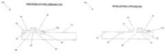
- FIG. 1 athere is schematically illustrated an apparatus 11 a which is a portable communications device with camera functionality.
- the camera functionalityprovides for (e.g. digitial) capture of an image of a scene by way of a (e.g. digital) camera 14 .
- the apparatus 11 aalso comprises a flash 12 to allow for illumination of the scene, if required.
- the flash 12provides for illumination by using light radiation, it can be considered to be a radiation source 12 .
- the apparatus 11 acomprises a spectometry module 11 b ( FIG. 1 c ).
- the modulecomprises a first waveguide 15 , a second waveguide 19 , an analyte region 16 , and a spectral dispersion element comprising a first diffraction grating 17 a .
- the spectrometry moduleis attached to be part of the apparatus 11 a such that it can be (e.g. slidably) moved between at least two positions to provide for at least two apparatus configurations.
- a first configurationFIG. 1 a
- the apparatus 11 aIn a first configuration ( FIG. 1 a ), the apparatus 11 a is configured for spectrometry, and in a second configuration ( FIG. 1 b ), the apparatus 11 a is configured to be able to perform regular camera functionality (i.e.
- the spectrometry module 11 bis moved between the two configurations to make use of/reveal the camera/flash according to the particular configuration in question.
- the module 11 bcan be considered to be moveably attached to the apparatus, such that the module 11 b is able to slide across the surface of the apparatus between the first and second configurations.
- the first waveguide 15is positioned to transmit radiation 20 from the radiation source 12 towards an analyte region 16 .
- the first diffraction grating 17 ais positioned to diffract radiation 20 from the analyte region 16 , towards the camera 14 .
- the camera 14can then receive the diffracted radiation (spectrum) from any analyte placed in the analyte region 16 .
- the received spectrumcan then be recorded by the camera for use in spectral analysis. It will be appreciated that the diffracted radiation forms a spectrum, one wavelength being diffracted at an angle that differs from that of another.
- FIG. 1 aschematically illustrates the first, spectrum capture, configuration wherein the first diffraction grating 17 a is positioned proximate to the camera 14 .
- FIG. 1 bschematically illustrates a second, image capture, configuration, wherein the the first diffraction grating 17 a is positioned away from the camera 14 .
- the diffraction grating 17 ais optically removed and/or separate from the camera, which thus allows the apparatus 11 a to be used to capture an image of an object/scene that is distant from the apparatus 11 a , and not associated with the analyte region 16 .
- the apparatus 11 ais used to capture a spectrum of an analyte that has been placed in or on the analyte region 16 .
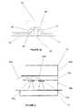
- the apparatus 11 a /module 11 bmay be configured such that the module can be completely removed from the apparatus 11 a to provide the second, image capture configuration, and then subsequently reattached to provide for the first, spectrum capture configuration.
- An exampleis shown schematically in FIG. 1 c , when in the second configuration, the apparatus, comprising the attachable module 11 b , need not be in contact with it; the module 11 b comprises the first waveguide 15 , second waveguide 19 , and first diffraction grating 17 a .
- the module/apparatuswould have complementary mating members (e.g. pins/guide recesses (not shown) which allow for such removal).
- the apparatus 11 a /module 11 bcomprises a radiation reflector 21 (e.g. mirror) configured to reflect radiation 20 from the radiation source 12 towards the first waveguide 15 .
- a radiation reflector 21e.g. mirror
- the apparatus 11 acomprises a pre-analyte interface 24 , schematically illustrated in FIG. 2 b , configured to deflect radiation 20 from the first waveguide 15 towards the analyte 26 .
- the apparatus 11 amay comprise a post-analyte radiation interface 25 configured to deflect radiation from the analyte 26 towards the second waveguide 19 .
- the second waveguide 19is configured to transmit radiation 20 from the analyte region 16 toward the first grating 17 a .
- the post- and pre-analyte interfaces 24 , 25may each be formed from different parts of a convex single lens 28 configured to deflect radiation 20 from the first waveguide 15 towards the analyte 26 , and configured to deflect radiation from the analyte 26 towards the second waveguide 19 .
- the apparatus 11 acomprises a second diffraction grating 17 b , schematically illustrated in FIG. 2 c , configured to diffract radiation having a second wavelength 20 b towards the camera 14 , and the first grating 17 a configured to diffract radiation having a first wavelength 20 a towards the camera 14 .
- the second waveguide 19may be configured such, that the first grating 17 a is formed in the second waveguide 19 .
- the second waveguide 19may be configured such that the first 17 a and second 17 b gratings are formed in the second waveguide 19 .
- the first and second waveguides 15 , 19each comprise a first refractive region 15 a , 19 a through which radiation 20 may propagate, and a second refractive region 15 b , 19 b that reflects radiation from the interface between the first and second refractive regions 15 a , 15 b .
- the refractive index of the first region 15 a , 19 amust be less than that of the second region 15 b , 19 b to ensure total internal reflection of the radiation 20 and hence transmission from radiation source 12 to analyte region 16 .
- Both the first and second refractive regions 19 a , 19 bmay comprise a glass selected from one or more of: silica, fluorozirconate, fluoroaluminate, chalcogenide, aluminosilicate, germanosilicate, phosphosilicate, and borosilicate glasses. If the second refractive region 15 b , 19 b comprises a glass, then it may be doped with a second dopant to raise the refractive index, selected from one or more of germanium dioxide and aluminium oxide.
- the first refractive region 15 a , 19 acomprises a glass, then it may be doped with a first dopant, to lower its refractive index, selected from one or more of fluorine one and boron trioxide.
- the waveguidemay comprise a polymer selected from one or more of: PMMA, an acrylate, an acrylic, a polystyrene, a siloxane, a polycarbonate, methylpentene, a terpolymer of acetonitrile, a butadiene, a styrene, and an allyl diglycol carbonate.
- the first refractive region 15 a , 19 amay comprise a fluorinated polymer to lower its refractive index relative to the second region 15 b , 19 b.
- the apparatus 11 acomprises a first grating 17 a , and a second grating 17 b , the dispersion element comprising the first and second gratings 17 a , 17 b , each grating 17 a , 17 b configured to diffract a wavelength, substantially perpendicularly from the grating 17 a , 17 b .
- the camera 14has two sensors 27 a , 27 b , each corresponding to one of the two gratings 17 a , 17 b , the gratings 17 a , 17 b and the camera 14 being configured such that each sensor 17 a , 17 b corresponds to the wavelength 18 a , 18 b diffracted by the gratings 17 a , 17 b , each sensor 17 a , 17 b receiving diffracted radiation only from the grating with which it corresponds.
- Each grating 17 a , 17 bmay have a period between 400-1000 nm.
- the gratingmay have a periodic topological surface profile, a profile depth being between 20 nm and 1000 nm.
- the topological profilemay be sinusoidal, or triangular. If the waveguide 15 , 19 comprises glass, then the topological profile may be written into a sacrificial resist layer coated on the glass by one or more of: photolithography, imprint lithography, e-beam lithography, and holography; followed by etching into the glass by: reactive ion etching, or atom etching. if the waveguide 15 , 19 comprises a thermosetting polymer, the topological profile may be fabricated by injection moulding, or thermal imprint lithography.
- the analyte region 16is configured to receive an analyte 26 , as illustrated in FIG. 2 e .
- the analyte region 16may comprise a surface onto, or above, which the analyte 26 may be placed.
- the analyte regionmay be configured to contain a gas/liquid.
- the analytemay comprise one or more of: a chemical, a biological sample, a food sample, an aqueous solution, a medical sample, a pharmaceutical product, a soil sample, and an agricultural sample.
- the analyte 26may comprise a human body part such as a finger that is placed on or in the analyte region.
- analyte region 16is optically transparent to receive radiation from the first waveguide 15 and provide it to the second waveguide 19 , and as such, such portions can be made from any suitable material, e.g. perspex or glass.
- an apparatuscan be considered to be the spectrometry module 11 b alone. In other embodiments, the apparatus could be considered to comprise the portable electronic device and the module 11 b .
- the cameramay record variation of the spectrum with time using a video clip.
- the radiation source 12may comprise a camera flash.
- the radiation source 12may comprise a white flash, or a colour changing LED that varies the wavelength of the radiation, transmitted to the analyte, with time. Such light would be suitable both for illumination of a scene as well as spectometry.
- the communication device 13may further comprise a touchscreen 31 .
- the communication device 13may comprise an antenna, transceiver, microphone and loudspeaker.
- the different functions discussed hereinmay be performed in a different order and/or concurrently with each other. Furthermore, if desired, one or more of the above-described functions may be optional or may be combined.
Landscapes
- Physics & Mathematics (AREA)
- Spectroscopy & Molecular Physics (AREA)
- General Physics & Mathematics (AREA)
- Investigating Or Analysing Materials By Optical Means (AREA)
- Investigating, Analyzing Materials By Fluorescence Or Luminescence (AREA)
Abstract
Description
The present application relates generally to spectrometry.
A spectrometer is typically used to assist in identification of analytes such as chemicals, medical samples, food samples, or biological samples. A spectrometer typically uses a radiation source to illuminate an analyte such that the radiation from the radiation source is then reflected from, or transmitted by, the analyte. The transmitted or reflected radiation can then be diffracted by a diffraction grating to yield a spectrum which is characteristic of the analyte. The charactersitc spectrum may then be detected by a detector to discern one or more characteristic properties of the analyte.
Various aspects of examples of the invention are set out in the claims.
According to a first aspect of the present invention, an apparatus comprising a waveguide and a spectral dispersion element, the apparatus being configured to be moveably attachable to a portable device, the portable device comprising a radiation sensing element and a radiation source, the apparatus being configured to be moveably attachable to the portable device to provide a first configuration in which the waveguide is positioned to transmit radiation from the radiation source towards an analyte region and/or from the analyte region towards the dispersion element; and such that the dispersion element is positioned to disperse radiation from the analyte region to form a spectrum which is provided towards the radiation sensing element for spectral analysis, and a second configuration in which the radiation sensing element and radiation source are able to capture and illuminate a scene for image capture.
According to a second aspect of the present invention, a method comprising:
- (i) providing a first configuration in which an apparatus, comprising a waveguide and a spectral dispersion element, is attached to a portable device, which comprises a radiation source and a radiation sensing element; such that the waveguide is positioned to transmit radiation from the radiation source towards an analyte region and/or from the analyte region towards the dispersion element; and such that the dispersion element is positioned to disperse radiation from the analyte region to form a spectrum which is provided towards the radiation sensing element for spectral analysis;
- (ii) transmitting radiation from the radiation source to the dispersion element via the analyte region to provide a spectrum for spectral analysis; and
- (iii) using the radiation sensing element to detect at least part of the spectrum.
For a more complete understanding of example embodiments of the present invention, reference is now made to the following descriptions taken in connection with the accompanying, drawings in which:
Various example embodiments of an apparatus according to the present disclosure will now be described by referring toFIGS. 1 through 3 of the drawings.
An apparatus such as a portable communication device (e.g. the so-called mobile phone, or Personal Digital Assistant (PDA)) typically comprises an antenna and associated hardware/software, to allow for communication. Increasingly, such devices comprise camera functionality. InFIG. 1 a. there is schematically illustrated anapparatus 11awhich is a portable communications device with camera functionality. The camera functionality provides for (e.g. digitial) capture of an image of a scene by way of a (e.g. digital)camera 14. As the camera captures light radiation, it can be considered to be aradiation sensing element 14. Theapparatus 11aalso comprises aflash 12 to allow for illumination of the scene, if required. As theflash 12 provides for illumination by using light radiation, it can be considered to be aradiation source 12.
In addition, theapparatus 11 a comprises a spectometry module11b(FIG. 1 c). The module comprises afirst waveguide 15, asecond waveguide 19, ananalyte region 16, and a spectral dispersion element comprising a first diffraction grating17a. The spectrometry module is attached to be part of theapparatus 11asuch that it can be (e.g. slidably) moved between at least two positions to provide for at least two apparatus configurations. In a first configuration (FIG. 1 a), theapparatus 11ais configured for spectrometry, and in a second configuration (FIG. 1 b), theapparatus 11ais configured to be able to perform regular camera functionality (i.e. capture of a photo of a scene). The spectrometry module11bis moved between the two configurations to make use of/reveal the camera/flash according to the particular configuration in question. In certain embodiments, the module11bcan be considered to be moveably attached to the apparatus, such that the module11bis able to slide across the surface of the apparatus between the first and second configurations.
In a first configuration of theapparatus 11a, thefirst waveguide 15 is positioned to transmitradiation 20 from theradiation source 12 towards ananalyte region 16. Furthermore, the first diffraction grating17ais positioned to diffractradiation 20 from theanalyte region 16, towards thecamera 14. Thecamera 14 can then receive the diffracted radiation (spectrum) from any analyte placed in theanalyte region 16. The received spectrum can then be recorded by the camera for use in spectral analysis. It will be appreciated that the diffracted radiation forms a spectrum, one wavelength being diffracted at an angle that differs from that of another.
As previously mentioned,FIG. 1 aschematically illustrates the first, spectrum capture, configuration wherein the first diffraction grating17ais positioned proximate to thecamera 14.FIG. 1 bschematically illustrates a second, image capture, configuration, wherein the the first diffraction grating17ais positioned away from thecamera 14. In the second configuration, the diffraction grating17a, is optically removed and/or separate from the camera, which thus allows theapparatus 11ato be used to capture an image of an object/scene that is distant from theapparatus 11a, and not associated with theanalyte region 16. In the first configuration, theapparatus 11ais used to capture a spectrum of an analyte that has been placed in or on theanalyte region 16.
Theapparatus 11a/module11bmay be configured such that the module can be completely removed from theapparatus 11ato provide the second, image capture configuration, and then subsequently reattached to provide for the first, spectrum capture configuration. An example is shown schematically inFIG. 1 c, when in the second configuration, the apparatus, comprising the attachable module11b, need not be in contact with it; the module11bcomprises thefirst waveguide 15,second waveguide 19, and first diffraction grating17a. In such embodiments, the module/apparatus would have complementary mating members (e.g. pins/guide recesses (not shown) which allow for such removal).
In a further embodiment (seeFIG. 2 a), theapparatus 11a/module11bcomprises a radiation reflector21 (e.g. mirror) configured to reflectradiation 20 from theradiation source 12 towards thefirst waveguide 15.
Theapparatus 11acomprises apre-analyte interface 24, schematically illustrated inFIG. 2 b, configured to deflectradiation 20 from thefirst waveguide 15 towards theanalyte 26. In the same, or different embodiment, theapparatus 11amay comprise apost-analyte radiation interface 25 configured to deflect radiation from theanalyte 26 towards thesecond waveguide 19. In such embodiments, thesecond waveguide 19 is configured to transmitradiation 20 from theanalyte region 16 toward the first grating17a. The post- andpre-analyte interfaces single lens 28 configured to deflectradiation 20 from thefirst waveguide 15 towards theanalyte 26, and configured to deflect radiation from theanalyte 26 towards thesecond waveguide 19.
In a further embodiment, theapparatus 11acomprises a second diffraction grating17b, schematically illustrated inFIG. 2 c, configured to diffract radiation having asecond wavelength 20btowards thecamera 14, and thefirst grating 17aconfigured to diffract radiation having afirst wavelength 20atowards thecamera 14. Thesecond waveguide 19 may be configured such, that thefirst grating 17ais formed in thesecond waveguide 19. Thesecond waveguide 19 may be configured such that the first17aand second17bgratings are formed in thesecond waveguide 19.
With reference toFIG. 2 a, the first andsecond waveguides refractive region radiation 20 may propagate, and a secondrefractive region refractive regions first region second region radiation 20 and hence transmission fromradiation source 12 to analyteregion 16. Both the first and secondrefractive regions refractive region refractive region second region refractive region second region
A further embodiment is described in relation toFIG. 2 d. As schematically illustrated inFIG. 2 d, theapparatus 11acomprises afirst grating 17a, and asecond grating 17b, the dispersion element comprising the first andsecond gratings radiation gratings FIG. 2 d, thecamera 14 has twosensors 27a,27b, each corresponding to one of the twogratings gratings camera 14 being configured such that eachsensor wavelength 18a,18bdiffracted by thegratings sensor waveguide waveguide
Theanalyte region 16 is configured to receive ananalyte 26, as illustrated inFIG. 2 e. Theanalyte region 16 may comprise a surface onto, or above, which theanalyte 26 may be placed. In certain embodiments, the analyte region may be configured to contain a gas/liquid. The analyte may comprise one or more of: a chemical, a biological sample, a food sample, an aqueous solution, a medical sample, a pharmaceutical product, a soil sample, and an agricultural sample. Theanalyte 26 may comprise a human body part such as a finger that is placed on or in the analyte region. It will be appreciated that at least a portion of theanalyte region 16 is optically transparent to receive radiation from thefirst waveguide 15 and provide it to thesecond waveguide 19, and as such, such portions can be made from any suitable material, e.g. perspex or glass.
It will be appreciated that, in certain cases, an apparatus according to the present disclosure can be considered to be the spectrometry module11balone. In other embodiments, the apparatus could be considered to comprise the portable electronic device and the module11b. The camera may record variation of the spectrum with time using a video clip. Theradiation source 12 may comprise a camera flash. Theradiation source 12 may comprise a white flash, or a colour changing LED that varies the wavelength of the radiation, transmitted to the analyte, with time. Such light would be suitable both for illumination of a scene as well as spectometry. Thecommunication device 13 may further comprise atouchscreen 31. Thecommunication device 13 may comprise an antenna, transceiver, microphone and loudspeaker.
Without in any way limiting the scope, interpretation, or application of the claims appearing below, a technical effect of one or more of the example embodiments is that the apparatus and assembly described herein are simple, compact, and robust.
If desired, the different functions discussed herein may be performed in a different order and/or concurrently with each other. Furthermore, if desired, one or more of the above-described functions may be optional or may be combined.
Although various aspects of the invention are set out in the independent claims, other aspects of the invention comprise other combinations of features from the described embodiments and/or the dependent claims with the features of the independent claims, and not solely the combinations explicitly set out in the claims.
It is also noted herein that while the above describes example embodiments of the invention, these descriptions should not be viewed in a limiting sense. Rather, there are several variations and modifications which may be made without departing from the scope of the present invention as defined in the appended claims.
Claims (12)
1. An apparatus comprising:
a waveguide:
a spectral dispersion element;
wherein the apparatus is configured to be moveably attachable to a portable radio communication device comprising a transmitter and a receiver, the portable radio communication device comprising a radiation sensing element and a radiation source, the apparatus being configured to be moveably attachable to the portable radio communication device to provide a first configuration in which the waveguide is positioned to transmit radiation from the radiation source towards an analyte region and/or from the analyte region towards the dispersion element, wherein the dispersion element comprises a plurality of diffraction gratings, each grating being configured to diffract radiation from the analyte region towards the radiation sensing element; and such that the dispersion element is positioned to disperse radiation from the analyte region to form a spectrum which is provided towards the radiation sensing element for spectral analysis, and a second configuration in which the radiation sensing element and radiation source are able to capture and illuminate a scene for image capture.
2. An apparatus according toclaim 1 , wherein the waveguide is configured to transmit radiation from the analyte region to the dispersion element, and wherein the waveguide is configured such that the dispersion element comprises a diffraction grating formed in the waveguide, the first diffraction grating being configured to diffract radiation from the analyte region towards the radiation sensing element.
3. An apparatus according toclaim 2 , wherein the grating and the waveguide are each configured such that nk0=kg; and λg=λ0/n, where n=refractive index of the waveguide, k0=wavevector of the radiation and λ0=wavelength of the radiation, kg=Bragg vector of the grating, λg=period of the grating.
4. An apparatus according toclaim 1 , wherein the apparatus comprises the analyte region; and the analyte region is configured to contain an analyte or is configured to comprise a surface onto which the analyte is placed.
5. An apparatus according toclaim 1 , wherein the apparatus is configured to be moveably attachable to a device such that the apparatus is moveable between the first configuration and the second configuration in which the apparatus is optically separate from the light sensing element.
6. An apparatus according toclaim 1 , wherein the apparatus is configured to be moveably attachable to a portable device such that the apparatus is moveable between the first configuration and the second configuration in which the apparatus is separate from the portable device.
7. An apparatus according toclaim 1 , wherein the apparatus is attached to the portable device and the radiation source comprises a camera flash.
8. An apparatus according toclaim 1 , wherein the apparatus is a module for a portable device.
9. A method comprising:
(i) providing a first configuration in which an apparatus, comprising a waveguide and a spectral dispersion element, is attached to a portable radio communication device comprising a transmitter and a receiver, which comprises a radiation source and a radiation sensing element; such that the waveguide is positioned to transmit radiation from the radiation source towards an analyte region and/or from the analyte region towards the dispersion element, wherein the dispersion element comprises a number of diffraction gratings, each grating being configured to diffract radiation from the analyte region towards the radiation sensing element; and such that the dispersion element is positioned to disperse radiation from the analyte region to form a spectrum which is provided towards the radiation sensing element for spectral analysis;
(ii) transmitting radiation from the radiation source to the dispersion element via the analyte region to provide a spectrum for spectral analysis; and
(iii) using the radiation sensing element to detect at least part of the spectrum.
10. A method according toclaim 9 , wherein the method comprises moving the apparatus from the first configuration to a second configuration in which the radiation sensing element and radiation source are able to capture and illuminate a scene for image capture.
11. A method according toclaim 9 , wherein the sensing element comprises a camera, and wherein the method comprises using the camera to record variation of the spectrum with time.
12. A method according toclaim 9 , wherein the portable device comprises a radio communication device.
Priority Applications (4)
| Application Number | Priority Date | Filing Date | Title |
|---|---|---|---|
| US12/939,987US8305577B2 (en) | 2010-11-04 | 2010-11-04 | Method and apparatus for spectrometry |
| CN201180053130.6ACN103189721B (en) | 2010-11-04 | 2011-09-19 | For spectrometric method and apparatus |
| EP11837617.7AEP2635880B1 (en) | 2010-11-04 | 2011-09-19 | Method and apparatus for spectrometry |
| PCT/FI2011/050803WO2012059622A1 (en) | 2010-11-04 | 2011-09-19 | Method and apparatus for spectrometry |
Applications Claiming Priority (1)
| Application Number | Priority Date | Filing Date | Title |
|---|---|---|---|
| US12/939,987US8305577B2 (en) | 2010-11-04 | 2010-11-04 | Method and apparatus for spectrometry |
Publications (2)
| Publication Number | Publication Date |
|---|---|
| US20120113422A1 US20120113422A1 (en) | 2012-05-10 |
| US8305577B2true US8305577B2 (en) | 2012-11-06 |
Family
ID=46019357
Family Applications (1)
| Application Number | Title | Priority Date | Filing Date |
|---|---|---|---|
| US12/939,987Active2031-02-05US8305577B2 (en) | 2010-11-04 | 2010-11-04 | Method and apparatus for spectrometry |
Country Status (4)
| Country | Link |
|---|---|
| US (1) | US8305577B2 (en) |
| EP (1) | EP2635880B1 (en) |
| CN (1) | CN103189721B (en) |
| WO (1) | WO2012059622A1 (en) |
Cited By (105)
| Publication number | Priority date | Publication date | Assignee | Title |
|---|---|---|---|---|
| US20080305795A1 (en)* | 2007-06-08 | 2008-12-11 | Tomoki Murakami | Information provision system |
| US9058653B1 (en) | 2011-06-10 | 2015-06-16 | Flir Systems, Inc. | Alignment of visible light sources based on thermal images |
| US9143703B2 (en) | 2011-06-10 | 2015-09-22 | Flir Systems, Inc. | Infrared camera calibration techniques |
| US9208542B2 (en) | 2009-03-02 | 2015-12-08 | Flir Systems, Inc. | Pixel-wise noise reduction in thermal images |
| US9207708B2 (en) | 2010-04-23 | 2015-12-08 | Flir Systems, Inc. | Abnormal clock rate detection in imaging sensor arrays |
| US9235876B2 (en) | 2009-03-02 | 2016-01-12 | Flir Systems, Inc. | Row and column noise reduction in thermal images |
| US9235023B2 (en) | 2011-06-10 | 2016-01-12 | Flir Systems, Inc. | Variable lens sleeve spacer |
| US9244280B1 (en) | 2014-03-25 | 2016-01-26 | Rockwell Collins, Inc. | Near eye display system and method for display enhancement or redundancy |
| US9244281B1 (en) | 2013-09-26 | 2016-01-26 | Rockwell Collins, Inc. | Display system and method using a detached combiner |
| US9274339B1 (en) | 2010-02-04 | 2016-03-01 | Rockwell Collins, Inc. | Worn display system and method without requiring real time tracking for boresight precision |
| US9292909B2 (en) | 2009-06-03 | 2016-03-22 | Flir Systems, Inc. | Selective image correction for infrared imaging devices |
| US9341846B2 (en) | 2012-04-25 | 2016-05-17 | Rockwell Collins Inc. | Holographic wide angle display |
| US9366864B1 (en) | 2011-09-30 | 2016-06-14 | Rockwell Collins, Inc. | System for and method of displaying information without need for a combiner alignment detector |
| USD765081S1 (en) | 2012-05-25 | 2016-08-30 | Flir Systems, Inc. | Mobile communications device attachment with camera |
| US9451183B2 (en) | 2009-03-02 | 2016-09-20 | Flir Systems, Inc. | Time spaced infrared image enhancement |
| US9473681B2 (en) | 2011-06-10 | 2016-10-18 | Flir Systems, Inc. | Infrared camera system housing with metalized surface |
| US9509924B2 (en) | 2011-06-10 | 2016-11-29 | Flir Systems, Inc. | Wearable apparatus with integrated infrared imaging module |
| US9507150B1 (en) | 2011-09-30 | 2016-11-29 | Rockwell Collins, Inc. | Head up display (HUD) using a bent waveguide assembly |
| US9517679B2 (en) | 2009-03-02 | 2016-12-13 | Flir Systems, Inc. | Systems and methods for monitoring vehicle occupants |
| US9521289B2 (en) | 2011-06-10 | 2016-12-13 | Flir Systems, Inc. | Line based image processing and flexible memory system |
| US9519089B1 (en) | 2014-01-30 | 2016-12-13 | Rockwell Collins, Inc. | High performance volume phase gratings |
| US9523852B1 (en) | 2012-03-28 | 2016-12-20 | Rockwell Collins, Inc. | Micro collimator system and method for a head up display (HUD) |
| US9635285B2 (en) | 2009-03-02 | 2017-04-25 | Flir Systems, Inc. | Infrared imaging enhancement with fusion |
| US9674458B2 (en) | 2009-06-03 | 2017-06-06 | Flir Systems, Inc. | Smart surveillance camera systems and methods |
| US9674413B1 (en) | 2013-04-17 | 2017-06-06 | Rockwell Collins, Inc. | Vision system and method having improved performance and solar mitigation |
| US9706137B2 (en) | 2011-06-10 | 2017-07-11 | Flir Systems, Inc. | Electrical cabinet infrared monitor |
| US9706139B2 (en) | 2011-06-10 | 2017-07-11 | Flir Systems, Inc. | Low power and small form factor infrared imaging |
| US9706138B2 (en) | 2010-04-23 | 2017-07-11 | Flir Systems, Inc. | Hybrid infrared sensor array having heterogeneous infrared sensors |
| US9715110B1 (en) | 2014-09-25 | 2017-07-25 | Rockwell Collins, Inc. | Automotive head up display (HUD) |
| US9716843B2 (en) | 2009-06-03 | 2017-07-25 | Flir Systems, Inc. | Measurement device for electrical installations and related methods |
| US9715067B1 (en) | 2011-09-30 | 2017-07-25 | Rockwell Collins, Inc. | Ultra-compact HUD utilizing waveguide pupil expander with surface relief gratings in high refractive index materials |
| US9723227B2 (en) | 2011-06-10 | 2017-08-01 | Flir Systems, Inc. | Non-uniformity correction techniques for infrared imaging devices |
| US9756264B2 (en) | 2009-03-02 | 2017-09-05 | Flir Systems, Inc. | Anomalous pixel detection |
| US9756262B2 (en) | 2009-06-03 | 2017-09-05 | Flir Systems, Inc. | Systems and methods for monitoring power systems |
| US9807319B2 (en) | 2009-06-03 | 2017-10-31 | Flir Systems, Inc. | Wearable imaging devices, systems, and methods |
| US9811884B2 (en) | 2012-07-16 | 2017-11-07 | Flir Systems, Inc. | Methods and systems for suppressing atmospheric turbulence in images |
| US9819880B2 (en) | 2009-06-03 | 2017-11-14 | Flir Systems, Inc. | Systems and methods of suppressing sky regions in images |
| US9843742B2 (en) | 2009-03-02 | 2017-12-12 | Flir Systems, Inc. | Thermal image frame capture using de-aligned sensor array |
| US9848134B2 (en) | 2010-04-23 | 2017-12-19 | Flir Systems, Inc. | Infrared imager with integrated metal layers |
| US9900526B2 (en) | 2011-06-10 | 2018-02-20 | Flir Systems, Inc. | Techniques to compensate for calibration drifts in infrared imaging devices |
| US9921105B2 (en) | 2015-02-05 | 2018-03-20 | International Business Machines Corporation | Mobile cellular spectroscopy |
| US9933684B2 (en) | 2012-11-16 | 2018-04-03 | Rockwell Collins, Inc. | Transparent waveguide display providing upper and lower fields of view having a specific light output aperture configuration |
| US9948872B2 (en) | 2009-03-02 | 2018-04-17 | Flir Systems, Inc. | Monitor and control systems and methods for occupant safety and energy efficiency of structures |
| US9961277B2 (en) | 2011-06-10 | 2018-05-01 | Flir Systems, Inc. | Infrared focal plane array heat spreaders |
| US9973692B2 (en) | 2013-10-03 | 2018-05-15 | Flir Systems, Inc. | Situational awareness by compressed display of panoramic views |
| US9986175B2 (en) | 2009-03-02 | 2018-05-29 | Flir Systems, Inc. | Device attachment with infrared imaging sensor |
| US9998697B2 (en) | 2009-03-02 | 2018-06-12 | Flir Systems, Inc. | Systems and methods for monitoring vehicle occupants |
| US10051210B2 (en) | 2011-06-10 | 2018-08-14 | Flir Systems, Inc. | Infrared detector array with selectable pixel binning systems and methods |
| US10079982B2 (en) | 2011-06-10 | 2018-09-18 | Flir Systems, Inc. | Determination of an absolute radiometric value using blocked infrared sensors |
| US10088675B1 (en) | 2015-05-18 | 2018-10-02 | Rockwell Collins, Inc. | Turning light pipe for a pupil expansion system and method |
| US10091439B2 (en) | 2009-06-03 | 2018-10-02 | Flir Systems, Inc. | Imager with array of multiple infrared imaging modules |
| US10108010B2 (en) | 2015-06-29 | 2018-10-23 | Rockwell Collins, Inc. | System for and method of integrating head up displays and head down displays |
| US10126552B2 (en) | 2015-05-18 | 2018-11-13 | Rockwell Collins, Inc. | Micro collimator system and method for a head up display (HUD) |
| US10156681B2 (en) | 2015-02-12 | 2018-12-18 | Digilens Inc. | Waveguide grating device |
| US10169666B2 (en) | 2011-06-10 | 2019-01-01 | Flir Systems, Inc. | Image-assisted remote control vehicle systems and methods |
| US10241330B2 (en) | 2014-09-19 | 2019-03-26 | Digilens, Inc. | Method and apparatus for generating input images for holographic waveguide displays |
| US10244190B2 (en) | 2009-03-02 | 2019-03-26 | Flir Systems, Inc. | Compact multi-spectrum imaging with fusion |
| US10247943B1 (en) | 2015-05-18 | 2019-04-02 | Rockwell Collins, Inc. | Head up display (HUD) using a light pipe |
| US10295824B2 (en) | 2017-01-26 | 2019-05-21 | Rockwell Collins, Inc. | Head up display with an angled light pipe |
| US10359736B2 (en) | 2014-08-08 | 2019-07-23 | Digilens Inc. | Method for holographic mastering and replication |
| US10389953B2 (en) | 2011-06-10 | 2019-08-20 | Flir Systems, Inc. | Infrared imaging device having a shutter |
| US10509241B1 (en) | 2009-09-30 | 2019-12-17 | Rockwell Collins, Inc. | Optical displays |
| US10545346B2 (en) | 2017-01-05 | 2020-01-28 | Digilens Inc. | Wearable heads up displays |
| US10598932B1 (en) | 2016-01-06 | 2020-03-24 | Rockwell Collins, Inc. | Head up display for integrating views of conformally mapped symbols and a fixed image source |
| US10642058B2 (en) | 2011-08-24 | 2020-05-05 | Digilens Inc. | Wearable data display |
| US10670876B2 (en) | 2011-08-24 | 2020-06-02 | Digilens Inc. | Waveguide laser illuminator incorporating a despeckler |
| US10678053B2 (en) | 2009-04-27 | 2020-06-09 | Digilens Inc. | Diffractive projection apparatus |
| US10690916B2 (en) | 2015-10-05 | 2020-06-23 | Digilens Inc. | Apparatus for providing waveguide displays with two-dimensional pupil expansion |
| US10725312B2 (en) | 2007-07-26 | 2020-07-28 | Digilens Inc. | Laser illumination device |
| US10732407B1 (en) | 2014-01-10 | 2020-08-04 | Rockwell Collins, Inc. | Near eye head up display system and method with fixed combiner |
| US10732569B2 (en) | 2018-01-08 | 2020-08-04 | Digilens Inc. | Systems and methods for high-throughput recording of holographic gratings in waveguide cells |
| US10747982B2 (en) | 2013-07-31 | 2020-08-18 | Digilens Inc. | Method and apparatus for contact image sensing |
| US10757308B2 (en) | 2009-03-02 | 2020-08-25 | Flir Systems, Inc. | Techniques for device attachment with dual band imaging sensor |
| US10760971B2 (en) | 2014-03-13 | 2020-09-01 | National University Of Singapore | Optical interference device |
| US10795160B1 (en) | 2014-09-25 | 2020-10-06 | Rockwell Collins, Inc. | Systems for and methods of using fold gratings for dual axis expansion |
| US10841508B2 (en) | 2011-06-10 | 2020-11-17 | Flir Systems, Inc. | Electrical cabinet infrared monitor systems and methods |
| US10859768B2 (en) | 2016-03-24 | 2020-12-08 | Digilens Inc. | Method and apparatus for providing a polarization selective holographic waveguide device |
| US10883927B2 (en)* | 2019-06-05 | 2021-01-05 | Taiwan Redeye Biomedical Inc. | Hemoglobin detecting device |
| US10890707B2 (en) | 2016-04-11 | 2021-01-12 | Digilens Inc. | Holographic waveguide apparatus for structured light projection |
| US10914950B2 (en) | 2018-01-08 | 2021-02-09 | Digilens Inc. | Waveguide architectures and related methods of manufacturing |
| US10942430B2 (en) | 2017-10-16 | 2021-03-09 | Digilens Inc. | Systems and methods for multiplying the image resolution of a pixelated display |
| US11256155B2 (en) | 2012-01-06 | 2022-02-22 | Digilens Inc. | Contact image sensor using switchable Bragg gratings |
| US11297264B2 (en) | 2014-01-05 | 2022-04-05 | Teledyne Fur, Llc | Device attachment with dual band imaging sensor |
| US11300795B1 (en) | 2009-09-30 | 2022-04-12 | Digilens Inc. | Systems for and methods of using fold gratings coordinated with output couplers for dual axis expansion |
| US11307432B2 (en) | 2014-08-08 | 2022-04-19 | Digilens Inc. | Waveguide laser illuminator incorporating a Despeckler |
| US11314084B1 (en) | 2011-09-30 | 2022-04-26 | Rockwell Collins, Inc. | Waveguide combiner system and method with less susceptibility to glare |
| US11320571B2 (en) | 2012-11-16 | 2022-05-03 | Rockwell Collins, Inc. | Transparent waveguide display providing upper and lower fields of view with uniform light extraction |
| US11366316B2 (en) | 2015-05-18 | 2022-06-21 | Rockwell Collins, Inc. | Head up display (HUD) using a light pipe |
| US11378732B2 (en) | 2019-03-12 | 2022-07-05 | DigLens Inc. | Holographic waveguide backlight and related methods of manufacturing |
| US11402801B2 (en) | 2018-07-25 | 2022-08-02 | Digilens Inc. | Systems and methods for fabricating a multilayer optical structure |
| US11442222B2 (en) | 2019-08-29 | 2022-09-13 | Digilens Inc. | Evacuated gratings and methods of manufacturing |
| US11487131B2 (en) | 2011-04-07 | 2022-11-01 | Digilens Inc. | Laser despeckler based on angular diversity |
| US11513350B2 (en) | 2016-12-02 | 2022-11-29 | Digilens Inc. | Waveguide device with uniform output illumination |
| US11543594B2 (en) | 2019-02-15 | 2023-01-03 | Digilens Inc. | Methods and apparatuses for providing a holographic waveguide display using integrated gratings |
| US11681143B2 (en) | 2019-07-29 | 2023-06-20 | Digilens Inc. | Methods and apparatus for multiplying the image resolution and field-of-view of a pixelated display |
| US11726329B2 (en) | 2015-01-12 | 2023-08-15 | Digilens Inc. | Environmentally isolated waveguide display |
| US11726332B2 (en) | 2009-04-27 | 2023-08-15 | Digilens Inc. | Diffractive projection apparatus |
| US11747568B2 (en) | 2019-06-07 | 2023-09-05 | Digilens Inc. | Waveguides incorporating transmissive and reflective gratings and related methods of manufacturing |
| US12092914B2 (en) | 2018-01-08 | 2024-09-17 | Digilens Inc. | Systems and methods for manufacturing waveguide cells |
| US12140764B2 (en) | 2019-02-15 | 2024-11-12 | Digilens Inc. | Wide angle waveguide display |
| US12158612B2 (en) | 2021-03-05 | 2024-12-03 | Digilens Inc. | Evacuated periodic structures and methods of manufacturing |
| US12210153B2 (en) | 2019-01-14 | 2025-01-28 | Digilens Inc. | Holographic waveguide display with light control layer |
| US12306585B2 (en) | 2018-01-08 | 2025-05-20 | Digilens Inc. | Methods for fabricating optical waveguides |
| US12397477B2 (en) | 2019-02-05 | 2025-08-26 | Digilens Inc. | Methods for compensating for optical surface nonuniformity |
| US12399326B2 (en) | 2021-01-07 | 2025-08-26 | Digilens Inc. | Grating structures for color waveguides |
Families Citing this family (8)
| Publication number | Priority date | Publication date | Assignee | Title |
|---|---|---|---|---|
| DE102011084348A1 (en)* | 2011-10-12 | 2013-04-18 | Carl Zeiss Microscopy Gmbh | Miniaturized opto-electronic system for spectral analysis |
| US10309954B2 (en)* | 2012-12-12 | 2019-06-04 | Green Domain Design Llc | Assay apparatus |
| US11320418B2 (en) | 2012-12-12 | 2022-05-03 | Iassay, Inc. | Modular hand-held point of care testing system |
| WO2015084332A1 (en) | 2013-12-03 | 2015-06-11 | Intel Corporation | Monolithic physically displaceable optical waveguides |
| US9500827B2 (en)* | 2014-06-27 | 2016-11-22 | Intel Corporation | Apparatus, method and system for spectrometry with a displaceable waveguide structure |
| US9400269B2 (en)* | 2014-09-22 | 2016-07-26 | The Royal Institution For The Advancement Of Learning/Mcgill University | Systems for detecting target chemicals and methods for their preparation and use |
| TWI544210B (en)* | 2014-10-21 | 2016-08-01 | 王基旆 | Portable electronic device, spectrometer combined with the device, and method for detecting the quality of the article by using the same |
| SG10201501196PA (en)* | 2015-02-16 | 2016-09-29 | Lighthaus Photonics Pte Ltd | Compact spectrometer |
Citations (11)
| Publication number | Priority date | Publication date | Assignee | Title |
|---|---|---|---|---|
| US5446534A (en) | 1993-03-05 | 1995-08-29 | Optical Solutions, Inc. | Broad band waveguide spectrometer |
| US5615008A (en) | 1994-12-21 | 1997-03-25 | Beckman Instruments, Inc. | Optical waveguide integrated spectrometer |
| US6289144B1 (en)* | 1995-05-12 | 2001-09-11 | Novartis Ag | Sensor platform and method for the parallel detection of a plurality of analytes using evanescently excited luminescence |
| WO2003100469A2 (en) | 2001-10-02 | 2003-12-04 | Alfred E. Mann Institute For Biomedical Engineering At The University Of Southern California | Internal biochemical sensing device |
| US20040248318A1 (en)* | 2003-01-30 | 2004-12-09 | Ciphergen Biosystems, Inc. | Apparatus for microfluidic processing and reading of biochip arrays |
| US20050147342A1 (en) | 2001-11-21 | 2005-07-07 | Kabushiki Kaisha Toshiba | Optical waveguide sensor, device, system and method for glucose measurement |
| US20060279732A1 (en) | 2005-05-24 | 2006-12-14 | Wang Sean X | Spectroscopic sensor on mobile phone |
| US20060292039A1 (en) | 2003-09-05 | 2006-12-28 | Kazuhiro Iida | Measuring system |
| WO2009070459A1 (en) | 2007-11-30 | 2009-06-04 | Jingyun Zhang | Miniature spectrometers working with cellular phones and other portable electronic devices |
| US20090295910A1 (en) | 2005-03-24 | 2009-12-03 | Jose Mir | Hyperspectral Imaging System and Methods Thereof |
| US7894693B2 (en)* | 2007-04-05 | 2011-02-22 | Eudyna Devices Inc. | Optical semiconductor device and method of controlling the same |
- 2010
- 2010-11-04USUS12/939,987patent/US8305577B2/enactiveActive
- 2011
- 2011-09-19WOPCT/FI2011/050803patent/WO2012059622A1/enactiveApplication Filing
- 2011-09-19EPEP11837617.7Apatent/EP2635880B1/enactiveActive
- 2011-09-19CNCN201180053130.6Apatent/CN103189721B/enactiveActive
Patent Citations (11)
| Publication number | Priority date | Publication date | Assignee | Title |
|---|---|---|---|---|
| US5446534A (en) | 1993-03-05 | 1995-08-29 | Optical Solutions, Inc. | Broad band waveguide spectrometer |
| US5615008A (en) | 1994-12-21 | 1997-03-25 | Beckman Instruments, Inc. | Optical waveguide integrated spectrometer |
| US6289144B1 (en)* | 1995-05-12 | 2001-09-11 | Novartis Ag | Sensor platform and method for the parallel detection of a plurality of analytes using evanescently excited luminescence |
| WO2003100469A2 (en) | 2001-10-02 | 2003-12-04 | Alfred E. Mann Institute For Biomedical Engineering At The University Of Southern California | Internal biochemical sensing device |
| US20050147342A1 (en) | 2001-11-21 | 2005-07-07 | Kabushiki Kaisha Toshiba | Optical waveguide sensor, device, system and method for glucose measurement |
| US20040248318A1 (en)* | 2003-01-30 | 2004-12-09 | Ciphergen Biosystems, Inc. | Apparatus for microfluidic processing and reading of biochip arrays |
| US20060292039A1 (en) | 2003-09-05 | 2006-12-28 | Kazuhiro Iida | Measuring system |
| US20090295910A1 (en) | 2005-03-24 | 2009-12-03 | Jose Mir | Hyperspectral Imaging System and Methods Thereof |
| US20060279732A1 (en) | 2005-05-24 | 2006-12-14 | Wang Sean X | Spectroscopic sensor on mobile phone |
| US7894693B2 (en)* | 2007-04-05 | 2011-02-22 | Eudyna Devices Inc. | Optical semiconductor device and method of controlling the same |
| WO2009070459A1 (en) | 2007-11-30 | 2009-06-04 | Jingyun Zhang | Miniature spectrometers working with cellular phones and other portable electronic devices |
Non-Patent Citations (5)
| Title |
|---|
| International Search Report in PCT Application PCT/FI2011/050803, dated Nov. 16, 2011. |
| Notification of Transmittal of the International Search Report and The Written Opinion of the International Searching Authority in PCT Application PCT/FI2011/050803, dated Nov. 16, 2011. |
| Rowe, C.J. et al. High reflectivity surface-relief gratings in single-mode optical fibers. IEEE Proceedings, Part J, Optoelectronics. 1987, vol. 134, pp. 192-202. |
| Schneier, Bruce; Applied Cryptography; 2nd ed. 1996 (15 pages). |
| Written Opinion of the International Searching Authority in PCT Application PCT/FI2011/050803, dated Nov. 16, 2011. |
Cited By (151)
| Publication number | Priority date | Publication date | Assignee | Title |
|---|---|---|---|---|
| US20080305795A1 (en)* | 2007-06-08 | 2008-12-11 | Tomoki Murakami | Information provision system |
| US10725312B2 (en) | 2007-07-26 | 2020-07-28 | Digilens Inc. | Laser illumination device |
| US9986175B2 (en) | 2009-03-02 | 2018-05-29 | Flir Systems, Inc. | Device attachment with infrared imaging sensor |
| US9208542B2 (en) | 2009-03-02 | 2015-12-08 | Flir Systems, Inc. | Pixel-wise noise reduction in thermal images |
| US9756264B2 (en) | 2009-03-02 | 2017-09-05 | Flir Systems, Inc. | Anomalous pixel detection |
| US9235876B2 (en) | 2009-03-02 | 2016-01-12 | Flir Systems, Inc. | Row and column noise reduction in thermal images |
| US9517679B2 (en) | 2009-03-02 | 2016-12-13 | Flir Systems, Inc. | Systems and methods for monitoring vehicle occupants |
| US9948872B2 (en) | 2009-03-02 | 2018-04-17 | Flir Systems, Inc. | Monitor and control systems and methods for occupant safety and energy efficiency of structures |
| US9998697B2 (en) | 2009-03-02 | 2018-06-12 | Flir Systems, Inc. | Systems and methods for monitoring vehicle occupants |
| US9635285B2 (en) | 2009-03-02 | 2017-04-25 | Flir Systems, Inc. | Infrared imaging enhancement with fusion |
| US10033944B2 (en) | 2009-03-02 | 2018-07-24 | Flir Systems, Inc. | Time spaced infrared image enhancement |
| US10757308B2 (en) | 2009-03-02 | 2020-08-25 | Flir Systems, Inc. | Techniques for device attachment with dual band imaging sensor |
| US9843742B2 (en) | 2009-03-02 | 2017-12-12 | Flir Systems, Inc. | Thermal image frame capture using de-aligned sensor array |
| US10244190B2 (en) | 2009-03-02 | 2019-03-26 | Flir Systems, Inc. | Compact multi-spectrum imaging with fusion |
| US9451183B2 (en) | 2009-03-02 | 2016-09-20 | Flir Systems, Inc. | Time spaced infrared image enhancement |
| US11726332B2 (en) | 2009-04-27 | 2023-08-15 | Digilens Inc. | Diffractive projection apparatus |
| US10678053B2 (en) | 2009-04-27 | 2020-06-09 | Digilens Inc. | Diffractive projection apparatus |
| US11175512B2 (en) | 2009-04-27 | 2021-11-16 | Digilens Inc. | Diffractive projection apparatus |
| US10091439B2 (en) | 2009-06-03 | 2018-10-02 | Flir Systems, Inc. | Imager with array of multiple infrared imaging modules |
| US9843743B2 (en) | 2009-06-03 | 2017-12-12 | Flir Systems, Inc. | Infant monitoring systems and methods using thermal imaging |
| US9756262B2 (en) | 2009-06-03 | 2017-09-05 | Flir Systems, Inc. | Systems and methods for monitoring power systems |
| US9716843B2 (en) | 2009-06-03 | 2017-07-25 | Flir Systems, Inc. | Measurement device for electrical installations and related methods |
| US9819880B2 (en) | 2009-06-03 | 2017-11-14 | Flir Systems, Inc. | Systems and methods of suppressing sky regions in images |
| US9292909B2 (en) | 2009-06-03 | 2016-03-22 | Flir Systems, Inc. | Selective image correction for infrared imaging devices |
| US9807319B2 (en) | 2009-06-03 | 2017-10-31 | Flir Systems, Inc. | Wearable imaging devices, systems, and methods |
| US9674458B2 (en) | 2009-06-03 | 2017-06-06 | Flir Systems, Inc. | Smart surveillance camera systems and methods |
| US11300795B1 (en) | 2009-09-30 | 2022-04-12 | Digilens Inc. | Systems for and methods of using fold gratings coordinated with output couplers for dual axis expansion |
| US10509241B1 (en) | 2009-09-30 | 2019-12-17 | Rockwell Collins, Inc. | Optical displays |
| US9274339B1 (en) | 2010-02-04 | 2016-03-01 | Rockwell Collins, Inc. | Worn display system and method without requiring real time tracking for boresight precision |
| US9848134B2 (en) | 2010-04-23 | 2017-12-19 | Flir Systems, Inc. | Infrared imager with integrated metal layers |
| US9706138B2 (en) | 2010-04-23 | 2017-07-11 | Flir Systems, Inc. | Hybrid infrared sensor array having heterogeneous infrared sensors |
| US9207708B2 (en) | 2010-04-23 | 2015-12-08 | Flir Systems, Inc. | Abnormal clock rate detection in imaging sensor arrays |
| US11487131B2 (en) | 2011-04-07 | 2022-11-01 | Digilens Inc. | Laser despeckler based on angular diversity |
| US9473681B2 (en) | 2011-06-10 | 2016-10-18 | Flir Systems, Inc. | Infrared camera system housing with metalized surface |
| US10169666B2 (en) | 2011-06-10 | 2019-01-01 | Flir Systems, Inc. | Image-assisted remote control vehicle systems and methods |
| US9723227B2 (en) | 2011-06-10 | 2017-08-01 | Flir Systems, Inc. | Non-uniformity correction techniques for infrared imaging devices |
| US9723228B2 (en) | 2011-06-10 | 2017-08-01 | Flir Systems, Inc. | Infrared camera system architectures |
| US10079982B2 (en) | 2011-06-10 | 2018-09-18 | Flir Systems, Inc. | Determination of an absolute radiometric value using blocked infrared sensors |
| US9706139B2 (en) | 2011-06-10 | 2017-07-11 | Flir Systems, Inc. | Low power and small form factor infrared imaging |
| US9706137B2 (en) | 2011-06-10 | 2017-07-11 | Flir Systems, Inc. | Electrical cabinet infrared monitor |
| US10051210B2 (en) | 2011-06-10 | 2018-08-14 | Flir Systems, Inc. | Infrared detector array with selectable pixel binning systems and methods |
| US10389953B2 (en) | 2011-06-10 | 2019-08-20 | Flir Systems, Inc. | Infrared imaging device having a shutter |
| US9538038B2 (en) | 2011-06-10 | 2017-01-03 | Flir Systems, Inc. | Flexible memory systems and methods |
| US10841508B2 (en) | 2011-06-10 | 2020-11-17 | Flir Systems, Inc. | Electrical cabinet infrared monitor systems and methods |
| US9521289B2 (en) | 2011-06-10 | 2016-12-13 | Flir Systems, Inc. | Line based image processing and flexible memory system |
| US9509924B2 (en) | 2011-06-10 | 2016-11-29 | Flir Systems, Inc. | Wearable apparatus with integrated infrared imaging module |
| US9900526B2 (en) | 2011-06-10 | 2018-02-20 | Flir Systems, Inc. | Techniques to compensate for calibration drifts in infrared imaging devices |
| US10250822B2 (en) | 2011-06-10 | 2019-04-02 | Flir Systems, Inc. | Wearable apparatus with integrated infrared imaging module |
| US9058653B1 (en) | 2011-06-10 | 2015-06-16 | Flir Systems, Inc. | Alignment of visible light sources based on thermal images |
| US9143703B2 (en) | 2011-06-10 | 2015-09-22 | Flir Systems, Inc. | Infrared camera calibration techniques |
| US9961277B2 (en) | 2011-06-10 | 2018-05-01 | Flir Systems, Inc. | Infrared focal plane array heat spreaders |
| US10230910B2 (en) | 2011-06-10 | 2019-03-12 | Flir Systems, Inc. | Infrared camera system architectures |
| US9716844B2 (en) | 2011-06-10 | 2017-07-25 | Flir Systems, Inc. | Low power and small form factor infrared imaging |
| US9235023B2 (en) | 2011-06-10 | 2016-01-12 | Flir Systems, Inc. | Variable lens sleeve spacer |
| US12306418B2 (en) | 2011-08-24 | 2025-05-20 | Rockwell Collins, Inc. | Wearable data display |
| US11287666B2 (en) | 2011-08-24 | 2022-03-29 | Digilens, Inc. | Wearable data display |
| US10670876B2 (en) | 2011-08-24 | 2020-06-02 | Digilens Inc. | Waveguide laser illuminator incorporating a despeckler |
| US10642058B2 (en) | 2011-08-24 | 2020-05-05 | Digilens Inc. | Wearable data display |
| US10401620B1 (en) | 2011-09-30 | 2019-09-03 | Rockwell Collins, Inc. | Waveguide combiner system and method with less susceptibility to glare |
| US9715067B1 (en) | 2011-09-30 | 2017-07-25 | Rockwell Collins, Inc. | Ultra-compact HUD utilizing waveguide pupil expander with surface relief gratings in high refractive index materials |
| US9507150B1 (en) | 2011-09-30 | 2016-11-29 | Rockwell Collins, Inc. | Head up display (HUD) using a bent waveguide assembly |
| US9599813B1 (en) | 2011-09-30 | 2017-03-21 | Rockwell Collins, Inc. | Waveguide combiner system and method with less susceptibility to glare |
| US9977247B1 (en) | 2011-09-30 | 2018-05-22 | Rockwell Collins, Inc. | System for and method of displaying information without need for a combiner alignment detector |
| US9366864B1 (en) | 2011-09-30 | 2016-06-14 | Rockwell Collins, Inc. | System for and method of displaying information without need for a combiner alignment detector |
| US11314084B1 (en) | 2011-09-30 | 2022-04-26 | Rockwell Collins, Inc. | Waveguide combiner system and method with less susceptibility to glare |
| US11256155B2 (en) | 2012-01-06 | 2022-02-22 | Digilens Inc. | Contact image sensor using switchable Bragg gratings |
| US9523852B1 (en) | 2012-03-28 | 2016-12-20 | Rockwell Collins, Inc. | Micro collimator system and method for a head up display (HUD) |
| US11460621B2 (en) | 2012-04-25 | 2022-10-04 | Rockwell Collins, Inc. | Holographic wide angle display |
| US10690915B2 (en) | 2012-04-25 | 2020-06-23 | Rockwell Collins, Inc. | Holographic wide angle display |
| US9341846B2 (en) | 2012-04-25 | 2016-05-17 | Rockwell Collins Inc. | Holographic wide angle display |
| USD765081S1 (en) | 2012-05-25 | 2016-08-30 | Flir Systems, Inc. | Mobile communications device attachment with camera |
| US9811884B2 (en) | 2012-07-16 | 2017-11-07 | Flir Systems, Inc. | Methods and systems for suppressing atmospheric turbulence in images |
| US12405507B2 (en) | 2012-11-16 | 2025-09-02 | Digilens Inc. | Transparent waveguide display with grating lamina that both couple and extract modulated light |
| US12276895B2 (en) | 2012-11-16 | 2025-04-15 | Rockwell Collins, Inc. | Transparent waveguide display with passive expander input bragg gratings with different angular diffraction efficiencies |
| US9933684B2 (en) | 2012-11-16 | 2018-04-03 | Rockwell Collins, Inc. | Transparent waveguide display providing upper and lower fields of view having a specific light output aperture configuration |
| US20180373115A1 (en)* | 2012-11-16 | 2018-12-27 | Digilens, Inc. | Transparent Waveguide Display |
| US11448937B2 (en) | 2012-11-16 | 2022-09-20 | Digilens Inc. | Transparent waveguide display for tiling a display having plural optical powers using overlapping and offset FOV tiles |
| US11320571B2 (en) | 2012-11-16 | 2022-05-03 | Rockwell Collins, Inc. | Transparent waveguide display providing upper and lower fields of view with uniform light extraction |
| US11815781B2 (en) | 2012-11-16 | 2023-11-14 | Rockwell Collins, Inc. | Transparent waveguide display |
| US9674413B1 (en) | 2013-04-17 | 2017-06-06 | Rockwell Collins, Inc. | Vision system and method having improved performance and solar mitigation |
| US9679367B1 (en) | 2013-04-17 | 2017-06-13 | Rockwell Collins, Inc. | HUD system and method with dynamic light exclusion |
| US10747982B2 (en) | 2013-07-31 | 2020-08-18 | Digilens Inc. | Method and apparatus for contact image sensing |
| US9244281B1 (en) | 2013-09-26 | 2016-01-26 | Rockwell Collins, Inc. | Display system and method using a detached combiner |
| US9973692B2 (en) | 2013-10-03 | 2018-05-15 | Flir Systems, Inc. | Situational awareness by compressed display of panoramic views |
| US11297264B2 (en) | 2014-01-05 | 2022-04-05 | Teledyne Fur, Llc | Device attachment with dual band imaging sensor |
| US10732407B1 (en) | 2014-01-10 | 2020-08-04 | Rockwell Collins, Inc. | Near eye head up display system and method with fixed combiner |
| US9519089B1 (en) | 2014-01-30 | 2016-12-13 | Rockwell Collins, Inc. | High performance volume phase gratings |
| US10760971B2 (en) | 2014-03-13 | 2020-09-01 | National University Of Singapore | Optical interference device |
| US9766465B1 (en) | 2014-03-25 | 2017-09-19 | Rockwell Collins, Inc. | Near eye display system and method for display enhancement or redundancy |
| US9244280B1 (en) | 2014-03-25 | 2016-01-26 | Rockwell Collins, Inc. | Near eye display system and method for display enhancement or redundancy |
| US10359736B2 (en) | 2014-08-08 | 2019-07-23 | Digilens Inc. | Method for holographic mastering and replication |
| US11307432B2 (en) | 2014-08-08 | 2022-04-19 | Digilens Inc. | Waveguide laser illuminator incorporating a Despeckler |
| US11709373B2 (en) | 2014-08-08 | 2023-07-25 | Digilens Inc. | Waveguide laser illuminator incorporating a despeckler |
| US11726323B2 (en) | 2014-09-19 | 2023-08-15 | Digilens Inc. | Method and apparatus for generating input images for holographic waveguide displays |
| US10241330B2 (en) | 2014-09-19 | 2019-03-26 | Digilens, Inc. | Method and apparatus for generating input images for holographic waveguide displays |
| US11579455B2 (en) | 2014-09-25 | 2023-02-14 | Rockwell Collins, Inc. | Systems for and methods of using fold gratings for dual axis expansion using polarized light for wave plates on waveguide faces |
| US10795160B1 (en) | 2014-09-25 | 2020-10-06 | Rockwell Collins, Inc. | Systems for and methods of using fold gratings for dual axis expansion |
| US9715110B1 (en) | 2014-09-25 | 2017-07-25 | Rockwell Collins, Inc. | Automotive head up display (HUD) |
| US11726329B2 (en) | 2015-01-12 | 2023-08-15 | Digilens Inc. | Environmentally isolated waveguide display |
| US11740472B2 (en) | 2015-01-12 | 2023-08-29 | Digilens Inc. | Environmentally isolated waveguide display |
| US9921105B2 (en) | 2015-02-05 | 2018-03-20 | International Business Machines Corporation | Mobile cellular spectroscopy |
| US10156681B2 (en) | 2015-02-12 | 2018-12-18 | Digilens Inc. | Waveguide grating device |
| US11703645B2 (en) | 2015-02-12 | 2023-07-18 | Digilens Inc. | Waveguide grating device |
| US12379547B2 (en) | 2015-02-12 | 2025-08-05 | Digilens Inc. | Waveguide grating device |
| US10527797B2 (en) | 2015-02-12 | 2020-01-07 | Digilens Inc. | Waveguide grating device |
| US10746989B2 (en) | 2015-05-18 | 2020-08-18 | Rockwell Collins, Inc. | Micro collimator system and method for a head up display (HUD) |
| US10126552B2 (en) | 2015-05-18 | 2018-11-13 | Rockwell Collins, Inc. | Micro collimator system and method for a head up display (HUD) |
| US10247943B1 (en) | 2015-05-18 | 2019-04-02 | Rockwell Collins, Inc. | Head up display (HUD) using a light pipe |
| US10088675B1 (en) | 2015-05-18 | 2018-10-02 | Rockwell Collins, Inc. | Turning light pipe for a pupil expansion system and method |
| US10698203B1 (en) | 2015-05-18 | 2020-06-30 | Rockwell Collins, Inc. | Turning light pipe for a pupil expansion system and method |
| US11366316B2 (en) | 2015-05-18 | 2022-06-21 | Rockwell Collins, Inc. | Head up display (HUD) using a light pipe |
| US10108010B2 (en) | 2015-06-29 | 2018-10-23 | Rockwell Collins, Inc. | System for and method of integrating head up displays and head down displays |
| US11754842B2 (en) | 2015-10-05 | 2023-09-12 | Digilens Inc. | Apparatus for providing waveguide displays with two-dimensional pupil expansion |
| US11281013B2 (en) | 2015-10-05 | 2022-03-22 | Digilens Inc. | Apparatus for providing waveguide displays with two-dimensional pupil expansion |
| US12405471B2 (en) | 2015-10-05 | 2025-09-02 | Digilens Inc. | Apparatus for providing waveguide displays with two-dimensional pupil expansion |
| US10690916B2 (en) | 2015-10-05 | 2020-06-23 | Digilens Inc. | Apparatus for providing waveguide displays with two-dimensional pupil expansion |
| US11215834B1 (en) | 2016-01-06 | 2022-01-04 | Rockwell Collins, Inc. | Head up display for integrating views of conformally mapped symbols and a fixed image source |
| US10598932B1 (en) | 2016-01-06 | 2020-03-24 | Rockwell Collins, Inc. | Head up display for integrating views of conformally mapped symbols and a fixed image source |
| US11604314B2 (en) | 2016-03-24 | 2023-03-14 | Digilens Inc. | Method and apparatus for providing a polarization selective holographic waveguide device |
| US10859768B2 (en) | 2016-03-24 | 2020-12-08 | Digilens Inc. | Method and apparatus for providing a polarization selective holographic waveguide device |
| US10890707B2 (en) | 2016-04-11 | 2021-01-12 | Digilens Inc. | Holographic waveguide apparatus for structured light projection |
| US12298513B2 (en) | 2016-12-02 | 2025-05-13 | Digilens Inc. | Waveguide device with uniform output illumination |
| US11513350B2 (en) | 2016-12-02 | 2022-11-29 | Digilens Inc. | Waveguide device with uniform output illumination |
| US11586046B2 (en) | 2017-01-05 | 2023-02-21 | Digilens Inc. | Wearable heads up displays |
| US12248150B2 (en) | 2017-01-05 | 2025-03-11 | Digilens Inc. | Wearable heads up displays |
| US11194162B2 (en) | 2017-01-05 | 2021-12-07 | Digilens Inc. | Wearable heads up displays |
| US10545346B2 (en) | 2017-01-05 | 2020-01-28 | Digilens Inc. | Wearable heads up displays |
| US10705337B2 (en) | 2017-01-26 | 2020-07-07 | Rockwell Collins, Inc. | Head up display with an angled light pipe |
| US10295824B2 (en) | 2017-01-26 | 2019-05-21 | Rockwell Collins, Inc. | Head up display with an angled light pipe |
| US10942430B2 (en) | 2017-10-16 | 2021-03-09 | Digilens Inc. | Systems and methods for multiplying the image resolution of a pixelated display |
| US12352960B2 (en) | 2018-01-08 | 2025-07-08 | Digilens Inc. | Waveguide architectures and related methods of manufacturing |
| US12366823B2 (en) | 2018-01-08 | 2025-07-22 | Digilens Inc. | Systems and methods for high-throughput recording of holographic gratings in waveguide cells |
| US12306585B2 (en) | 2018-01-08 | 2025-05-20 | Digilens Inc. | Methods for fabricating optical waveguides |
| US12092914B2 (en) | 2018-01-08 | 2024-09-17 | Digilens Inc. | Systems and methods for manufacturing waveguide cells |
| US10732569B2 (en) | 2018-01-08 | 2020-08-04 | Digilens Inc. | Systems and methods for high-throughput recording of holographic gratings in waveguide cells |
| US10914950B2 (en) | 2018-01-08 | 2021-02-09 | Digilens Inc. | Waveguide architectures and related methods of manufacturing |
| US11402801B2 (en) | 2018-07-25 | 2022-08-02 | Digilens Inc. | Systems and methods for fabricating a multilayer optical structure |
| US12210153B2 (en) | 2019-01-14 | 2025-01-28 | Digilens Inc. | Holographic waveguide display with light control layer |
| US12397477B2 (en) | 2019-02-05 | 2025-08-26 | Digilens Inc. | Methods for compensating for optical surface nonuniformity |
| US12140764B2 (en) | 2019-02-15 | 2024-11-12 | Digilens Inc. | Wide angle waveguide display |
| US11543594B2 (en) | 2019-02-15 | 2023-01-03 | Digilens Inc. | Methods and apparatuses for providing a holographic waveguide display using integrated gratings |
| US11378732B2 (en) | 2019-03-12 | 2022-07-05 | DigLens Inc. | Holographic waveguide backlight and related methods of manufacturing |
| US10883927B2 (en)* | 2019-06-05 | 2021-01-05 | Taiwan Redeye Biomedical Inc. | Hemoglobin detecting device |
| US12271035B2 (en) | 2019-06-07 | 2025-04-08 | Digilens Inc. | Waveguides incorporating transmissive and reflective gratings and related methods of manufacturing |
| US11747568B2 (en) | 2019-06-07 | 2023-09-05 | Digilens Inc. | Waveguides incorporating transmissive and reflective gratings and related methods of manufacturing |
| US11681143B2 (en) | 2019-07-29 | 2023-06-20 | Digilens Inc. | Methods and apparatus for multiplying the image resolution and field-of-view of a pixelated display |
| US11899238B2 (en) | 2019-08-29 | 2024-02-13 | Digilens Inc. | Evacuated gratings and methods of manufacturing |
| US11592614B2 (en) | 2019-08-29 | 2023-02-28 | Digilens Inc. | Evacuated gratings and methods of manufacturing |
| US11442222B2 (en) | 2019-08-29 | 2022-09-13 | Digilens Inc. | Evacuated gratings and methods of manufacturing |
| US12399326B2 (en) | 2021-01-07 | 2025-08-26 | Digilens Inc. | Grating structures for color waveguides |
| US12158612B2 (en) | 2021-03-05 | 2024-12-03 | Digilens Inc. | Evacuated periodic structures and methods of manufacturing |
Also Published As
| Publication number | Publication date |
|---|---|
| EP2635880B1 (en) | 2022-09-28 |
| US20120113422A1 (en) | 2012-05-10 |
| EP2635880A1 (en) | 2013-09-11 |
| WO2012059622A1 (en) | 2012-05-10 |
| EP2635880A4 (en) | 2015-07-29 |
| CN103189721A (en) | 2013-07-03 |
| CN103189721B (en) | 2016-01-20 |
Similar Documents
| Publication | Publication Date | Title |
|---|---|---|
| US8305577B2 (en) | Method and apparatus for spectrometry | |
| US11353362B2 (en) | Integration of optical components within a folded optical path | |
| Hussain et al. | Smartphone-based optical spectroscopic platforms for biomedical applications: a review | |
| EP2304483B1 (en) | Retro-reflective structures | |
| TWI658261B (en) | Prism-coupling systems and methods for characterizing curved parts | |
| CN114341600A (en) | Optical measurement equipment including internal spectral reference | |
| CN107407598A (en) | Glass waveguide spectrophotometer | |
| CN105260708A (en) | Detection apparatus, electronic equipment, and information processing method | |
| JP2017527045A (en) | Image acquisition device, terminal device, and image acquisition method | |
| US11698302B2 (en) | Apparatus for optical applications, spectrometer system and method for producing an apparatus for optical applications | |
| US11255727B2 (en) | Nanostructure based article, optical sensor and analytical instrument and method of forming same | |
| Tan et al. | Optical fiber speckle spectrometer based on reversed-lens smartphone microscope | |
| Komai et al. | Compact spectroscopic sensor using a visible arrayed waveguide grating | |
| CN212722608U (en) | Portable surface plasma resonance biochemical detection device based on mobile phone platform | |
| CN111062336A (en) | Fingerprint identification terminal equipment | |
| TW200407603A (en) | Fabrication system for liquid crystal display device and method of fabricating liquid crystal display device using the same | |
| KR20100026165A (en) | Optical joy stick and portable electronic device having the same | |
| Mattelin et al. | An imprinted polymer-based guided mode resonance grating sensor | |
| WO2016093425A1 (en) | Optical system for optical sensor and photo sensor including same | |
| de la Cruz-González et al. | Design and development of multi-sensor based on all fiber NXN twisted plastic optical fiber | |
| Walters | Advanced FBG fabrication for challenging applications | |
| Rezwan et al. | PCF Based Optical Fiber Designing for Sensing in Terahertz Spectrum | |
| Lee et al. | Experimental and theoretical characterization of optical signal out-coupling through V-grooved optical fiber cladding | |
| Komai et al. | Spectroscopic sensing using a visible arrayed-waveguide grating | |
| TWI453527B (en) | Electronic device |
Legal Events
| Date | Code | Title | Description |
|---|---|---|---|
| AS | Assignment | Owner name:NOKIA CORPORATION, FINLAND Free format text:ASSIGNMENT OF ASSIGNORS INTEREST;ASSIGNORS:KIVIOJA, JANI;ANDREW, PIERS;BOWER, CHRIS;AND OTHERS;REEL/FRAME:025656/0048 Effective date:20101214 | |
| STCF | Information on status: patent grant | Free format text:PATENTED CASE | |
| AS | Assignment | Owner name:NOKIA TECHNOLOGIES OY, FINLAND Free format text:ASSIGNMENT OF ASSIGNORS INTEREST;ASSIGNOR:NOKIA CORPORATION;REEL/FRAME:035468/0384 Effective date:20150116 | |
| FPAY | Fee payment | Year of fee payment:4 | |
| MAFP | Maintenance fee payment | Free format text:PAYMENT OF MAINTENANCE FEE, 8TH YEAR, LARGE ENTITY (ORIGINAL EVENT CODE: M1552); ENTITY STATUS OF PATENT OWNER: LARGE ENTITY Year of fee payment:8 | |
| MAFP | Maintenance fee payment | Free format text:PAYMENT OF MAINTENANCE FEE, 12TH YEAR, LARGE ENTITY (ORIGINAL EVENT CODE: M1553); ENTITY STATUS OF PATENT OWNER: LARGE ENTITY Year of fee payment:12 |