US8305360B2 - Sensing circuit for capacitive touch panel - Google Patents
Sensing circuit for capacitive touch panelDownload PDFInfo
- Publication number
- US8305360B2 US8305360B2US12/554,635US55463509AUS8305360B2US 8305360 B2US8305360 B2US 8305360B2US 55463509 AUS55463509 AUS 55463509AUS 8305360 B2US8305360 B2US 8305360B2
- Authority
- US
- United States
- Prior art keywords
- capacitance
- sensing
- noise
- unit
- reference signal
- Prior art date
- Legal status (The legal status is an assumption and is not a legal conclusion. Google has not performed a legal analysis and makes no representation as to the accuracy of the status listed.)
- Active, expires
Links
Images


Classifications
- G—PHYSICS
- G06—COMPUTING OR CALCULATING; COUNTING
- G06F—ELECTRIC DIGITAL DATA PROCESSING
- G06F3/00—Input arrangements for transferring data to be processed into a form capable of being handled by the computer; Output arrangements for transferring data from processing unit to output unit, e.g. interface arrangements
- G06F3/01—Input arrangements or combined input and output arrangements for interaction between user and computer
- G06F3/03—Arrangements for converting the position or the displacement of a member into a coded form
- G06F3/041—Digitisers, e.g. for touch screens or touch pads, characterised by the transducing means
- G06F3/044—Digitisers, e.g. for touch screens or touch pads, characterised by the transducing means by capacitive means
- G—PHYSICS
- G06—COMPUTING OR CALCULATING; COUNTING
- G06F—ELECTRIC DIGITAL DATA PROCESSING
- G06F3/00—Input arrangements for transferring data to be processed into a form capable of being handled by the computer; Output arrangements for transferring data from processing unit to output unit, e.g. interface arrangements
- G06F3/01—Input arrangements or combined input and output arrangements for interaction between user and computer
- G06F3/03—Arrangements for converting the position or the displacement of a member into a coded form
- G06F3/041—Digitisers, e.g. for touch screens or touch pads, characterised by the transducing means
- G06F3/0416—Control or interface arrangements specially adapted for digitisers
- G06F3/0418—Control or interface arrangements specially adapted for digitisers for error correction or compensation, e.g. based on parallax, calibration or alignment
- G06F3/04182—Filtering of noise external to the device and not generated by digitiser components
Definitions
- the present inventiongenerally relates to a sensing circuit, and more particularly to a sensing circuit for a capacitive touch panel.
- touch panelApplications of conventional touch panels are widely used, for example, mobile phones, touch screens for public information, automatic teller machines (ATMs) and so on.
- ATMsautomatic teller machines
- the intuitive operations of a touch panelcan be substituted for the functions of a keyboard and a mouse; therefore, the touch panel is quite convenient in use.
- FIG. 1 and FIG. 2illustrate two types of capacitive touch panels 150 , 250 for detecting a touch position.
- the capacitive touch panel 150comprises a plurality of sensing lines in the X-axis direction and in the Y-axis direction, that is, the sensing lines X 1 -X 4 and Y 1 -Y 4 .
- Each of the sensing lines X 1 -X 4 and Y 1 -Y 4has a plurality of sensing electrodes (not shown).
- the sensing capacitance of each sensing electrodeis represented as C SENSE . When no touch event occurs, the sensing capacitance C SENSE is zero.
- the capacitive touch panel 150 in FIG. 1detects the touch position by sequentially scanning each of the sensing lines X 1 -X 4 and Y 1 -Y 4 . As shown in FIG. 1 , the scanning sequence is from the sensing line X 1 to the sensing line X 4 , and then from the sensing line Y 1 to the sensing line Y 4 . When the intersection point of the sensing line X 4 and the sensing line Y 1 is touched, for example, the touch position can be detected by a change of the sensing capacitance C SENSE .
- the capacitive touch panel 250also comprises a plurality of sensing lines in the X-axis direction and in the Y-axis direction, that is, the sensing lines X 1 -X 4 and Y 1 -Y 4 .
- the scanning sequenceis from the sensing line X 1 to the sensing line X 4
- the stimulating signalis sequentially inputted from the sensing line Y 1 to the sensing line Y 4 . That is, the stimulating signal is inputted to the sensing line Y 1
- the scanning sequenceis from the sensing line X 1 to X 4 .
- a sensing capacitance C TRANSrepresents a coupling capacitance between the sensing line X 1 and the sensing line Y 1 .
- the sensing capacitance C TRANShas different values at the intersection point of the sensing line X 1 and the sensing line Y 1 being touched or untouched. Similar to FIG. 1 , the touch position can be detected by a change of the sensing capacitance C TRANS .
- FIG. 3illustrates a block diagram of a conventional sensing circuit 100 .
- the sensing circuit 100comprises a sensing unit 102 (a sensing electrode), a sensing signal generating unit 104 , and an integrator 106 .
- the sensing unit 102has the sensing capacitance C SENSE as shown in FIG. 1 or the sensing capacitance C TRANS as shown in FIG. 2 to indicate that a touch event has occurred or not.
- the sensing signal generating unit 104generates a sensing signal according to the change of the sensing capacitance.
- the sensing signalis a voltage signal and inputted to the integrator 106 to be integrated.
- the integrator 106outputs an integrated result, and the touch position can be determined by the integrated result.
- the sensing unit 102is disposed on a sensing electrode substrate (not shown), and the sensing signal generating unit 104 and the integrator 106 are disposed on an array substrate of a liquid crystal display panel (not shown).
- a common electrode(not shown) is disposed between the sensing electrode substrate and the array substrate of the liquid crystal display panel for providing a required voltage level when the liquid crystal display panel operates. When the liquid crystal display panel operates, a common voltage provided by the common electrode is not clear. That is, the common voltage has the noise.
- the noiseis generated when a source bus of the liquid crystal display panel is driven to be pre-charged.
- the noiseis also generated when switches of the liquid crystal display panel are turned on and off.
- the noiseenters the sensing circuit 100 in FIG. 3 , causing the sensing circuit 100 to fail to detect the touch position or resulting in detection errors.
- a primary objective of the present inventionis to provide a sensing circuit for a capacitive touch panel.
- the noiseis differentially processed through two paths which have the same electrical conditions with each other. The noise is then decreased significantly, and a sensing signal can be detected correctly therefore.
- the sensing circuit for the capacitive touch panelcomprises a sensing signal part, a reference signal part, and an integrator.
- the sensing signal partgenerates a sensing signal according to a capacitance of the capacitive touch panel and a noise which is received by the sensing signal part.
- the capacitance of the capacitive touch panel at a touched conditionis different from the capacitance of the capacitive touch panel at an untouched condition.
- the reference signal partreceives the noise and outputs a reference signal.
- the reference signal parthas the same electrical conditions as the sensing signal part.
- the integratorreceives the sensing signal and the reference signal, and it subtracts the reference signal from the sensing signal to generate an output signal.
- the sensing circuit for the capacitive touch panelcomprises a sensing signal path, a reference signal path, and a first differential amplifier.
- the sensing signal pathgenerates a sensing signal according to a capacitance of the capacitive touch panel and a noise which is received by the sensing signal path.
- the capacitance of the capacitive touch panel at a touched conditionis different from the capacitance of the capacitive touch panel at an untouched condition.
- the reference signal pathreceives the noise and outputs a reference signal.
- the reference signal pathhas the same electrical conditions as the sensing signal path.
- the first differential amplifierreceives the sensing signal and the reference signal, and it subtracts the reference signal from the sensing signal to generate an output signal.
- FIG. 1 and FIG. 2illustrate two types of capacitive touch panels for detecting a touch position
- FIG. 3illustrates a block diagram of a conventional sensing circuit
- FIG. 4illustrates a functional block diagram according to a sensing circuit of the present invention
- FIG. 5illustrates a circuit diagram according to a first embodiment shown in FIG. 4 ;
- FIG. 6illustrates a circuit diagram according to a second embodiment shown in FIG. 4 ;
- FIG. 7illustrates a diagram of an electronic apparatus comprising a capacitive touch panel.
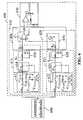
- FIG. 4illustrates a functional block diagram according to a sensing circuit 400 of the present invention.
- the sensing circuit 400is capable of decreasing influence of a noise S NOISE generated by a common electrode 440 in a capacitive touch panel (not shown).
- the sensing circuit 400basically comprises a sensing signal part 411 , a reference signal part 421 , and an integrator 406 .
- the sensing signal part 411generates a sensing signal S T according to a capacitance of the capacitive touch panel and the noise S NOISE which is received by the sensing signal part 411 .
- the capacitance of the capacitive touch panel at a touched conditionis different from the capacitance of the capacitive touch panel at an untouched condition.
- the reference signal part 421receives the noise S NOISE and outputs a reference signal S NOISE ′.
- the reference signal part 421is simulated to have the same electrical conditions as the sensing signal part 411 .
- the integrator 406receives the sensing signal S T and the reference signal S NOISE ′.
- the function of the integrator 406is to integrate a difference between signals fed to two inputs of the integrator 406 . As a result, the integrator 406 subtracts the reference signal S NOISE ′ from the sensing signal S T to generate an output signal S OUT .
- the reference signal part 421has a capacitance substantially equal to a capacitance of the sensing signal part 411 at the untouched condition.
- the sensing signal part 411 and the reference signal part 421have the same electrical conditions.
- the reference signal part 421has a plurality of electrical elements, and the electrical elements are connected to simulate equivalent circuits of the sensing signal part 411 so that both the reference signal part 421 and the sensing signal part 411 have approximately the same electrical characteristics, such as resistance, capacitance, and so on.
- the objective of the above-mentionedis to make the noise S NOISE pass through the same circuits so that noise values inputted to the integrator 406 are the same after the noise S NOISE passes the sensing signal part 411 and the reference signal part 421 , respectively.
- FIG. 5illustrates a circuit diagram according to a first embodiment shown in FIG. 4 .
- This embodimentis a sensing circuit 500 utilized in a capacitive touch panel where scan lines are sequentially scanned from one direction to the other direction.
- a sensing signal part 511comprises a sensing unit 512 and a sensing signal generating unit 514 .
- a reference signal part 521comprises a reference unit 522 and a reference signal generating unit 524 .
- the sensing unit 512has a sensing capacitance which is represented as C SENSE .
- C SENSEsensing capacitance
- the sensing capacitance C SENSE of the sensing unit 512is zero.
- the sensing capacitance C SENSEis not zero.
- the sensing unit 512further has a parasitic capacitance.
- the parasitic capacitanceis an equivalent capacitance between a common electrode 540 and a sensing electrode substrate (not shown), and it is represented as C PAR1 .
- a noise S NOISE of the common electrode 540is coupled to the sensing unit 512 through the parasitic capacitance C PAR1 .
- the sensing unit 512receives the noise S NOISE through the parasitic capacitance C PAR1 .
- the sensing unit 512has a first equivalent capacitance or a second equivalent capacitance.
- the first equivalent capacitanceis an equivalent capacitance of the capacitance of the capacitive touch panel at the touched condition (i.e. the sensing capacitance C SENSE ) and the parasitic capacitance C PAR1 .
- the second equivalent capacitanceis an equivalent capacitance of the capacitance of the capacitive touch panel at the untouched condition (i.e. the sensing capacitance C SENSE is zero) and the parasitic capacitance C PAR1 .
- the sensing signal generating unit 514is coupled to the sensing unit 512 .
- the sensing signal generating unit 514generates a sensing signal S T according to the first equivalent capacitance and the noise S NOISE or according to the second equivalent capacitance and the noise S NOISE .
- the control signal V TOGGLEis an added signal for reacting the touched condition or the untouched condition (i.e. the sensing capacitance C SENSE ). That is, the control signal V TOGGLE is utilized to transform the first equivalent capacitance or the second equivalent capacitance into a signal change so as to indicate that the capacitive touch panel is touched or untouched.
- the control signal V TOGGLEis coupled to the sensing signal generating unit 514 through a first coupling capacitor C C1 .
- the noise S NOISEis coupled thereto through the parasitic capacitance C PAR1 so that generates an S 1NOISE at the node 1 .
- the S 1NOISEis obtained by the following equation (1):
- the noise S NOISEpasses through the sensing signal part 511 , in addition, the present invention establishes the other path for the noise S NOISE of the common electrode 540 to pass through.
- the reference unit 522receives the noise S NOISE and has a third equivalent capacitance.
- the third capacitancesimulates the capacitance of the capacitive touch panel at the untouched condition and the parasitic capacitance C PAR1 . That is, the third equivalent capacitance is equal to the second equivalent capacitance of the sensing unit 512 . Therefore, the reference unit 522 has a capacitor C PAR2 to simulate the parasitic capacitance C PAR1 .
- the noise S NOISEis coupled to the reference unit 522 through the capacitor C PAR2 .
- the parasitic capacitance C PAR1is the equivalent capacitance between the common electrode 540 and the sensing electrode substrate.
- the parasitic capacitance C PAR1can be obtained by measuring.
- the capacitor C PAR2is an added capacitor which has the same capacitance as the parasitic capacitance C PAR1 .
- the reference signal generating unit 524has the same circuits as the sensing signal generating unit 514 , and the reference signal generating unit 524 outputs a reference signal S NOISE ′ according to the third equivalent capacitance of the reference unit 522 and the noise S NOISE .
- the reference signal generating unit 524has an added second coupling capacitor C C2 .
- the control signal V TOGGLEis also coupled to the reference signal generating unit 524 through the second coupling capacitor C C2 . Accordingly, the electrical conditions of the reference signal part 521 are the same as the electrical conditions of the sensing signal part 511 .
- an S 2NOISE at a node 2is:
- the capacitance of the capacitor C PAR2is substantially equal to the parasitic capacitance C PAR1
- the capacitance of second coupling capacitor C C2is substantially equal to the capacitance of the first coupling capacitor C C1 , therefore:
- a signal difference inputted to two inputs of the integrator 506is:
- the sensing signal part 511preferably comprises a first filter 518 coupled between the sensing signal generating unit 514 and the integrator 506 for filtering out high-frequency components of the sensing signal S T generated by the sensing signal generating unit 514 .
- the reference signal part 521preferably comprises a second filter 528 coupled between the reference signal generating unit 524 and the integrator 506 .
- the second filter 528has the same circuits as the first filter 518 , and the second filter 528 filters out high-frequency components of the reference signal S NOISE ′.
- the first filter 518comprises a third resistor R 3 coupled between the sensing signal generating unit 514 and the integrator 506 , and a third capacitor C 3 coupled between the integrator 506 and a ground.
- the second filter 528comprises a fourth resistor R 4 coupled between reference signal generating unit 524 and the integrator 506 , and a fourth capacitor C 4 coupled between the integrator 506 and a ground.
- a resistance of the third resistor R 3is substantially equal to a resistance of the fourth resistor R 4
- a capacitance of the third capacitor C 3is substantially equal to a capacitance of the fourth capacitor C 4 .
- the integrator 506comprises a first differential amplifier 532 , a first resistor R 1 , and a first capacitor C 1 .
- the first differential amplifier 532has an inverting input ( ⁇ ), a non-inverting input (+), and an output 4 .
- the first resistor R 1is coupled between the sensing signal part 511 and the inverting input ( ⁇ ).
- the first capacitor C 1is coupled between the inverting input ( ⁇ ) and the output 4 .
- the integrator 506further comprises a ground match unit 536 .
- the ground match unit 536is utilized to make the circuits inputted to the non-inverting input (+) the same as the circuits inputted to the inverting circuits ( ⁇ ).
- the ground match unit 536comprises a second resistor R 2 and a second capacitor C 2 .
- a resistance of the second resistor R 2must be designed the same as a resistance of the first resistor R 1
- a capacitance of the second capacitor C 2must be designed the same as a capacitance of the first capacitor C 1 .
- the second resistor R 2is coupled between the reference signal part 521 and the non-inverting input (+) of the first differential amplifier 532 .
- the second capacitor C 2is coupled between the non-inverting input (+) of the first differential amplifier 532 and a ground.
- the sensing signal S Tis generated according to the touched condition and the noise S NOISE or according to the untouched condition and the noise S NOISE .
- the pathcan be regarded as a sensing signal path 510 .
- the reference signal part 521 , the second resistor R 2 of the integrator 506 and the second capacitor C 2 of the integrator 506together constitute the other path for the noise S NOISE to pass through.
- the other pathcan be regarded as a reference signal path 520 .
- the reference signal path 520simulates the sensing signal path 510 so as to have the same electrical conditions as the sensing signal path 510 .
- the output 4 of the integrator 506can be coupled to an amplifying unit 530 for amplifying an output signal S OUT generated by the integrator 506 .
- the amplifying unit 530comprises a second differential amplifier 534 , a fifth resistor R 5 , and a sixth resistor R 6 .
- the second differential amplifier 534comprises an inverting input ( ⁇ ), a non-inverting input (+), and an output 3 .
- the non-inverting input (+)is coupled to the output 4 of the integrator 506 .
- the fifth resistor R 5is coupled between the inverting input ( ⁇ ) of the second differential amplifier 534 and a ground.
- the sixth resistor R 6is coupled between the inverting input ( ⁇ ) of the second differential amplifier 534 and the output 3 .
- a switch SW 1 of the sensing signal generating unit 514is utilized to switch different scan lines.
- Each of the scan linescomprises a plurality of sensing units 512 .
- the remaining elements including the integrator 506 , the first filter 518 , the reference unit 522 , the reference signal generating unit 524 , the ground match unit 536 , the second filter 528 , and the amplifying unit 530are shared by all the scan lines.
- the sensing signal generating unit 514 , the first filter 518 , the reference signal part 521 , the integrator 506 , and the amplifying unit 530are usually disposed on the array substrate of the liquid crystal display panel or disposed apart from the array substrate of the liquid crystal display panel.
- each sensing unit 512is a sensing electrode in the capacitive touch panel and disposed on the sensing electrode substrate.
- FIG. 6illustrates a circuit diagram according to a second embodiment shown in FIG. 4 .
- This embodimentis a sensing circuit 600 utilized in a capacitive touch panel where scan lines in only one direction are scanned and a stimulating signal is inputted to scan lines in the other direction.
- a sensing signal part 611comprises a sensing unit 612 and a sensing signal generating unit 614 .
- a reference signal part 621comprises a reference unit 622 and a reference signal generating unit 624 .
- the sensing unit 612When the capacitive touch panel is touched, the sensing unit 612 has a sensing capacitance which is represented as C TRANS .
- a capacitance of the capacitive touch panel at an untouched conditionthat is, the capacitance that the reference unit 622 simulates the capacitance of the capacitive touch panel at the untouched condition is represented as C TRANS ′.
- the sensing unit 612further has parasitic capacitances.
- the parasitic capacitancesare equivalent capacitances between a common electrode 640 and a sensing electrode substrate (not shown), and represented as C PAR3 and C PAR5 .
- a noise S NOISE of the common electrode 640is coupled to the sensing unit 612 through the parasitic capacitance C PAR3 .
- the sensing unit 612receives the noise S NOISE through the parasitic capacitance C PAR3 .
- the sensing unit 612has a first equivalent capacitance or a second equivalent capacitance.
- the first equivalent capacitanceis an equivalent capacitance of the capacitance of the capacitive touch panel at a touched condition (i.e. the sensing capacitance C TRANS ), the parasitic capacitance C PAR3 , and the parasitic capacitance C PAR5 .
- the second equivalent capacitanceis an equivalent capacitance of the capacitance of the capacitive touch panel at the untouched condition (i.e. the capacitance C TRANS ′), the parasitic capacitance C PAR3 , and the parasitic capacitance C PAR5 .
- the sensing signal generating unit 614is coupled to the sensing unit 612 .
- the sensing signal generating unit 614generates a sensing signal S T according to the first equivalent capacitance and the noise S NOISE or according to the second equivalent capacitance and the noise S NOISE .
- the control signal V TOGGLEis an added signal for reacting the touched condition or the untouched condition (i.e. the sensing capacitance C TRANS ). That is, the control signal V TOGGLE is utilized to transform the first equivalent capacitance or the second equivalent capacitance into a signal change so as to indicate that the capacitive touch panel is touched or untouched.
- the control signal V TOGGLEis directly inputted to the sensing unit 612 and the sensing signal generating unit 614 .
- the noise S NOISEis coupled thereto through the parasitic capacitance C PAR3 so that generates an S 5NOISE at the node 5 .
- the S 5NOISEis obtained by the following equation (3):
- the noise S NOISEpasses through the sensing signal part 611 , in addition, the present invention establishes the other path for the noise S NOISE of the common electrode 640 to pass through.
- the reference signal 622receives the noise S NOISE and has a third equivalent capacitance.
- the third capacitancesimulates the capacitance of the capacitive touch panel at the untouched condition (C TRANS ′), the parasitic capacitance C par3 , and the parasitic capacitance C PAR5 . That is, the third equivalent capacitance is equal to the second equivalent capacitance of the sensing unit 612 . Therefore, the reference unit 622 has capacitors C PAR4 , C PAR6 to simulate the parasitic capacitances C PAR3 , C PAR5 , respectively.
- the noise S NOISEis coupled to the reference unit 622 through the capacitor C PAR4 .
- the capacitors C PAR4 , C PAR6are added capacitors which have the same capacitances as the parasitic capacitances C PAR3 , C PAR5 , respectively.
- the reference signal generating unit 624has the same circuits as the sensing signal generating unit 614 , and the reference signal generating unit 624 outputs a reference signal S NOISE ′ according to the third equivalent capacitance of the reference unit 622 and the noise S NOISE .
- the control signal V TOGGLEis also inputted to the reference unit 622 and the reference signal generating unit 624 . Accordingly, the electrical conditions of the reference signal part 621 are the same as the electrical conditions of the sensing signal part 611 .
- the noise S NOISEpasses through both the reference signal part 621 and the sensing signal part 611 .
- an S 6NOISE at a node 6is:
- the capacitance of the capacitor C PAR4is substantially equal to the capacitance of the parasitic capacitance C PAR3 , therefore:
- a signal difference inputted to two inputs of the integrator 606is:
- the noise S NOISEcan be eliminated to increase sensitivity of the sensing circuit 600 after the integrator 606 integrates.
- a first filter 618 , a second filter 628 , the integrator 606 , a ground match unit 636 , and an amplifying unit 630are the same as the first embodiment shown in FIG. 5 , and are not repeated herein.
- the sensing signal part 611 , a seventh resistor R 7 of the integrator 606 and a seventh capacitor C 7 of the integrator 606together constitute one complete path for the sensing signal S T to pass through.
- the sensing signal S Tis generated according to the touched condition and the noise S NOISE or according to the untouched condition and the noise S NOISE .
- the pathcan be regarded as a sensing signal path 610 .
- the reference signal part 621 , the eighth resistor R 8 of the integrator 606 and the eighth capacitor C 8 of the integrator 606together constitute the other path for the noise S NOISE to pass through.
- the other pathcan be regarded as a reference signal path 620 .
- the reference signal path 620simulates the sensing signal path 610 so as to have the same electrical conditions as the sensing signal path 610 .
- the noiseis inputted to the two inputs of the differential amplifier through the sensing signal path and the reference signal path which have the same electrical conditions. After the differential amplifier subtracts the noise which passes through the two paths, the noise component in the sensing signal can be decreased significantly. As a result, the output of the differential amplifier only remains the sensing signal which is generated by the sensing signal generating unit, and the sensing signal can be detected correctly so that sensitivity and accuracy of the sensing circuits are increased.
- FIG. 7illustrates a diagram of an electronic apparatus 700 comprising a capacitive touch panel 750 .
- the capacitive touch panel 750comprises one of the sensing circuits 400 , 500 , and 600 .
- the capacitive touch panel 750comprising one of the sensing circuits 400 , 500 , and 600 can be a part of the electronic apparatus 700 .
- the electronic apparatus 700comprises the capacitive touch panel 750 and a power supply 740 .
- the power supply 740is coupled to the capacitive touch panel 750 for providing power for the capacitive touch panel 750 .
- the electronic apparatusis a mobile phone, a digital camera, a Personal Digital Assistant, a notebook, a desktop computer, a television, a Global Positioning System, a vehicle display, an aeronautical display, or a portable digital video disc (DVD) player.
- a mobile phonea digital camera
- a Personal Digital Assistanta notebook
- a desktop computera television
- a Global Positioning Systema vehicle display
- an aeronautical displayor a portable digital video disc (DVD) player.
- DVDportable digital video disc
Landscapes
- Engineering & Computer Science (AREA)
- General Engineering & Computer Science (AREA)
- Theoretical Computer Science (AREA)
- Human Computer Interaction (AREA)
- Physics & Mathematics (AREA)
- General Physics & Mathematics (AREA)
- Position Input By Displaying (AREA)
Abstract
Description
The noise SNOISEcan be eliminated to increase sensitivity of the
Claims (18)
Priority Applications (1)
| Application Number | Priority Date | Filing Date | Title |
|---|---|---|---|
| US12/554,635US8305360B2 (en) | 2008-09-08 | 2009-09-04 | Sensing circuit for capacitive touch panel |
Applications Claiming Priority (5)
| Application Number | Priority Date | Filing Date | Title |
|---|---|---|---|
| US9521408P | 2008-09-08 | 2008-09-08 | |
| TW98110713ATWI420374B (en) | 2008-09-08 | 2009-03-31 | Sensing circuit for capacitive touch panel and electronic device using the same |
| TW98110713A | 2009-03-31 | ||
| TW098110713 | 2009-03-31 | ||
| US12/554,635US8305360B2 (en) | 2008-09-08 | 2009-09-04 | Sensing circuit for capacitive touch panel |
Publications (2)
| Publication Number | Publication Date |
|---|---|
| US20100060610A1 US20100060610A1 (en) | 2010-03-11 |
| US8305360B2true US8305360B2 (en) | 2012-11-06 |
Family
ID=41798854
Family Applications (1)
| Application Number | Title | Priority Date | Filing Date |
|---|---|---|---|
| US12/554,635Active2031-06-09US8305360B2 (en) | 2008-09-08 | 2009-09-04 | Sensing circuit for capacitive touch panel |
Country Status (1)
| Country | Link |
|---|---|
| US (1) | US8305360B2 (en) |
Cited By (12)
| Publication number | Priority date | Publication date | Assignee | Title |
|---|---|---|---|---|
| US9268989B2 (en) | 2012-05-18 | 2016-02-23 | Apple Inc. | Capacitive sensor packaging |
| US9305959B2 (en) | 2013-06-05 | 2016-04-05 | Apple Inc. | Biometric sensor chip having distributed sensor and control circuitry |
| US9460332B1 (en) | 2013-09-09 | 2016-10-04 | Apple Inc. | Capacitive fingerprint sensor including an electrostatic lens |
| US20170063340A1 (en)* | 2015-03-26 | 2017-03-02 | Pixart Imaging Inc. | Programmable band-pass filter circuit of analog front-end used for capacitance detection |
| US9697409B2 (en) | 2013-09-10 | 2017-07-04 | Apple Inc. | Biometric sensor stack structure |
| US9740343B2 (en) | 2012-04-13 | 2017-08-22 | Apple Inc. | Capacitive sensing array modulation |
| US9830018B2 (en) | 2015-11-06 | 2017-11-28 | Industrial Technology Research Institute | Touch control apparatus and noise compensating circuit and method thereof |
| US9883822B2 (en) | 2013-06-05 | 2018-02-06 | Apple Inc. | Biometric sensor chip having distributed sensor and control circuitry |
| US9984270B2 (en) | 2013-08-05 | 2018-05-29 | Apple Inc. | Fingerprint sensor in an electronic device |
| US10606400B2 (en) | 2017-11-28 | 2020-03-31 | Industrial Technology Research Institute | Touch panel driving apparatus |
| US10628654B2 (en) | 2013-09-09 | 2020-04-21 | Apple Inc. | Capacitive sensing array having electrical isolation |
| US20200409506A1 (en)* | 2015-03-26 | 2020-12-31 | Pixart Imaging Inc. | Capacitive touch device with high sensitivity and low power consumption |
Families Citing this family (59)
| Publication number | Priority date | Publication date | Assignee | Title |
|---|---|---|---|---|
| KR101658991B1 (en)* | 2009-06-19 | 2016-09-22 | 삼성전자주식회사 | Touch panel and electronic device including the touch panel |
| KR101667801B1 (en)* | 2009-06-19 | 2016-10-20 | 삼성전자주식회사 | Touch panel and electronic device including the touch panel |
| KR101657215B1 (en)* | 2009-09-08 | 2016-09-19 | 삼성디스플레이 주식회사 | Display device including touch panel device and coupling-noise elliminating method |
| US8842079B2 (en)* | 2009-10-09 | 2014-09-23 | Egalax—Empia Technology Inc. | Method and device for determining a touch or touches |
| KR101616875B1 (en)* | 2010-01-07 | 2016-05-02 | 삼성전자주식회사 | Touch panel and electronic device including the touch panel |
| KR101631892B1 (en)* | 2010-01-28 | 2016-06-21 | 삼성전자주식회사 | Touch panel and electronic device including the touch panel |
| KR20110091380A (en)* | 2010-02-05 | 2011-08-11 | 삼성전자주식회사 | Noise compensation method and device of touch panel |
| JP5427648B2 (en)* | 2010-03-02 | 2014-02-26 | 株式会社ジャパンディスプレイ | Coordinate input device and display device including the same |
| KR101710523B1 (en)* | 2010-03-22 | 2017-02-27 | 삼성전자주식회사 | Touch panel and electronic device including the touch panel |
| KR20110112128A (en)* | 2010-04-06 | 2011-10-12 | 삼성전자주식회사 | Parasitic capacitance compensation method and apparatus of touch panel |
| JP5523191B2 (en)* | 2010-04-30 | 2014-06-18 | 株式会社ジャパンディスプレイ | Display device with touch detection function |
| TWI433016B (en) | 2010-04-30 | 2014-04-01 | Elan Microelectronics Corp | The capacitive touch panel sensing unit, and a sensing circuit sensing method |
| TWI414977B (en)* | 2010-05-18 | 2013-11-11 | Au Optronics Corp | Touch detecting method and flat display with in-cell touch panel |
| US8547359B2 (en) | 2010-06-21 | 2013-10-01 | Pixart Imaging Inc. | Capacitive touchscreen system with switchable charge acquisition circuit |
| US8274491B2 (en) | 2010-06-21 | 2012-09-25 | Pixart Imaging Inc. | Capacitive touchscreen signal acquisition without panel reset |
| TW201205398A (en)* | 2010-07-30 | 2012-02-01 | Chimei Innolux Corp | Display system having capacitive touch panel and manufacturing method thereof |
| KR101809191B1 (en) | 2010-10-11 | 2018-01-18 | 삼성전자주식회사 | Touch panel |
| KR101735715B1 (en) | 2010-11-23 | 2017-05-15 | 삼성전자주식회사 | Input sensing circuit and touch panel including the input sensing circuit |
| JP4955116B1 (en) | 2010-12-28 | 2012-06-20 | シャープ株式会社 | Touch panel system and electronic device |
| WO2012108911A1 (en)* | 2011-02-07 | 2012-08-16 | Cypress Semiconductor Corporation | Noise filtering devices, systems and methods for capacitance sensing devices |
| US9317158B2 (en)* | 2011-03-08 | 2016-04-19 | Synaptics Incorporated | Baseline management for input devices |
| KR101784436B1 (en)* | 2011-04-18 | 2017-10-11 | 삼성전자주식회사 | Touch panel and driving device for the touch panel |
| TWI456467B (en)* | 2011-05-20 | 2014-10-11 | Au Optronics Corp | Operating method of capacitive touch panel and touch control barrier-type 3d display device |
| US9013448B2 (en) | 2011-06-22 | 2015-04-21 | Sharp Kabushiki Kaisha | Touch panel system and electronic device |
| US9465492B2 (en) | 2011-06-22 | 2016-10-11 | Sharp Kabushiki Kaisha | Touch panel system and electronic device |
| EP2724214B1 (en) | 2011-06-22 | 2018-09-19 | Sharp Kabushiki Kaisha | Touch panel system and electronic device |
| CN102880327B (en)* | 2011-07-12 | 2016-03-30 | 宸鸿光电科技股份有限公司 | Touch screen touch circuit and touch pressure point detection method |
| US9088255B2 (en)* | 2011-08-15 | 2015-07-21 | Innolux Corporation | Sensing devices and display devices using a plurality of differential amplifiers and sensing circuits to minimize the time to detect presence of an object |
| KR101341924B1 (en)* | 2011-10-21 | 2013-12-19 | 포항공과대학교 산학협력단 | capacitance-measuring type touch sensor |
| JP5389888B2 (en) | 2011-10-25 | 2014-01-15 | シャープ株式会社 | Touch panel system and electronic device |
| US9444452B2 (en) | 2012-02-24 | 2016-09-13 | Parade Technologies, Ltd. | Frequency hopping algorithm for capacitance sensing devices |
| KR101328277B1 (en)* | 2012-03-30 | 2013-11-14 | 삼성전기주식회사 | Apparatus and method for sensing touch input |
| US20130300690A1 (en)* | 2012-04-25 | 2013-11-14 | Silicon Works Co., Ltd. | Control circuit of touch screen and noise removing method |
| US9244572B2 (en)* | 2012-05-04 | 2016-01-26 | Blackberry Limited | Electronic device including touch-sensitive display and method of detecting touches |
| KR101444524B1 (en) | 2012-07-09 | 2014-09-24 | 삼성전기주식회사 | Apparatus and method for sensing capacitance, and touchscreen apparatus |
| US9329738B2 (en)* | 2012-09-10 | 2016-05-03 | Apple Inc. | Determination and reduction of parasitic capacitance variation due to display noise |
| TWI489360B (en)* | 2013-01-25 | 2015-06-21 | Pixart Imaging Inc | Capacitive touch panel, sensing method thereof, touch device and inut apparatus |
| US9442598B2 (en)* | 2013-02-08 | 2016-09-13 | Synaptics Incorporated | Detecting interference in an input device having electrodes |
| JP6194606B2 (en)* | 2013-03-22 | 2017-09-13 | セイコーエプソン株式会社 | Detection device, sensor, gyro sensor, electronic device, and moving object |
| US9436324B2 (en) | 2013-11-04 | 2016-09-06 | Blackberry Limited | Electronic device including touch-sensitive display and method of detecting touches |
| KR20250002802A (en)* | 2013-11-29 | 2025-01-07 | 가부시키가이샤 한도오따이 에네루기 켄큐쇼 | Data processing device and driving method thereof |
| US9256333B2 (en)* | 2014-04-15 | 2016-02-09 | Samsung Electronics Co., Ltd. | Method and apparatus for reducing noise in capacitive touch interfaces |
| TWI550495B (en)* | 2015-03-26 | 2016-09-21 | 原相科技股份有限公司 | Capacitive touch device with high sensitivity and operating method thereof |
| TWI594152B (en)* | 2015-04-22 | 2017-08-01 | 友達光電股份有限公司 | Touching sensing device |
| US10120509B2 (en)* | 2015-12-29 | 2018-11-06 | Stmicroelectronics Asia Pacific Pte Ltd | Common mode noise reduction in capacitive touch sensing |
| TWI581167B (en)* | 2016-03-29 | 2017-05-01 | 矽創電子股份有限公司 | Noise suppression circuit |
| US10408870B2 (en) | 2016-06-28 | 2019-09-10 | Himax Technologies Limited | Capacitor sensor apparatus and sensing method thereof |
| CN107659289B (en)* | 2016-07-25 | 2020-12-11 | 原相科技股份有限公司 | Programmable Band-Pass Filter Circuit for Analog Front-End Circuits for Capacitive Sensing |
| KR102090508B1 (en)* | 2016-12-29 | 2020-03-19 | 선전 구딕스 테크놀로지 컴퍼니, 리미티드 | Touch system and its power circuit |
| CN109144305B (en)* | 2017-06-27 | 2021-07-27 | 原相科技股份有限公司 | High-sensitivity capacitive touch device and operation method thereof |
| TWI649682B (en)* | 2017-11-10 | 2019-02-01 | 大陸商北京集創北方科技股份有限公司 | Linear displacement noise suppression algorithm for touch and display drive integration system and touch display panel using the method to realize a touch display function |
| US11054942B2 (en)* | 2018-04-05 | 2021-07-06 | Synaptics Incorporated | Noise suppression circuit |
| TWI735184B (en)* | 2020-03-17 | 2021-08-01 | 友達光電股份有限公司 | Display driver circuit and display device having the same |
| US11703983B2 (en)* | 2020-03-25 | 2023-07-18 | Sensortek Technology Corp | Capacitance sensing circuit |
| US12105910B2 (en) | 2020-05-27 | 2024-10-01 | Novatek Microelectronics Corp. | Touch sensing method and electronic device |
| CN113741724B (en)* | 2020-05-27 | 2024-08-13 | 联咏科技股份有限公司 | Touch sensing method and electronic device |
| US11635853B2 (en) | 2020-05-27 | 2023-04-25 | Novatek Microelectronics Corp. | Touch sensing method with noise reduction |
| CN114327114B (en)* | 2020-09-30 | 2023-10-20 | 华为技术有限公司 | Electronic equipment, control method thereof, touch control system and chip system |
| CN116880715B (en)* | 2023-09-05 | 2023-11-17 | 合肥创发微电子有限公司 | Touch sensing circuit |
Citations (3)
| Publication number | Priority date | Publication date | Assignee | Title |
|---|---|---|---|---|
| US20070120831A1 (en)* | 2005-11-28 | 2007-05-31 | Mahowald Peter H | Neutralizing elecromagnetic noise for a capacitive input device |
| US20090231294A1 (en) | 2008-03-12 | 2009-09-17 | Tpo Displays Corp. | Image display systems |
| US20100013779A1 (en) | 2008-07-15 | 2010-01-21 | Tpo Displays Corp. | Systems for displaying images |
- 2009
- 2009-09-04USUS12/554,635patent/US8305360B2/enactiveActive
Patent Citations (3)
| Publication number | Priority date | Publication date | Assignee | Title |
|---|---|---|---|---|
| US20070120831A1 (en)* | 2005-11-28 | 2007-05-31 | Mahowald Peter H | Neutralizing elecromagnetic noise for a capacitive input device |
| US20090231294A1 (en) | 2008-03-12 | 2009-09-17 | Tpo Displays Corp. | Image display systems |
| US20100013779A1 (en) | 2008-07-15 | 2010-01-21 | Tpo Displays Corp. | Systems for displaying images |
Cited By (20)
| Publication number | Priority date | Publication date | Assignee | Title |
|---|---|---|---|---|
| US9740343B2 (en) | 2012-04-13 | 2017-08-22 | Apple Inc. | Capacitive sensing array modulation |
| US9880675B2 (en) | 2012-04-13 | 2018-01-30 | Apple Inc. | Capacitive sensing array modulation |
| US9576178B2 (en) | 2012-05-18 | 2017-02-21 | Apple Inc. | Capacitive sensor packaging |
| US10423815B2 (en) | 2012-05-18 | 2019-09-24 | Apple Inc. | Capacitive sensor packaging |
| US10783347B2 (en) | 2012-05-18 | 2020-09-22 | Apple Inc. | Capacitive sensor packaging |
| US9268989B2 (en) | 2012-05-18 | 2016-02-23 | Apple Inc. | Capacitive sensor packaging |
| US10007832B2 (en) | 2012-05-18 | 2018-06-26 | Apple Inc. | Capacitive sensor packaging |
| US10007833B2 (en) | 2012-05-18 | 2018-06-26 | Apple Inc. | Capacitive sensor packaging |
| US9305959B2 (en) | 2013-06-05 | 2016-04-05 | Apple Inc. | Biometric sensor chip having distributed sensor and control circuitry |
| US9883822B2 (en) | 2013-06-05 | 2018-02-06 | Apple Inc. | Biometric sensor chip having distributed sensor and control circuitry |
| US9984270B2 (en) | 2013-08-05 | 2018-05-29 | Apple Inc. | Fingerprint sensor in an electronic device |
| US9460332B1 (en) | 2013-09-09 | 2016-10-04 | Apple Inc. | Capacitive fingerprint sensor including an electrostatic lens |
| US10628654B2 (en) | 2013-09-09 | 2020-04-21 | Apple Inc. | Capacitive sensing array having electrical isolation |
| US9697409B2 (en) | 2013-09-10 | 2017-07-04 | Apple Inc. | Biometric sensor stack structure |
| US10063214B2 (en)* | 2015-03-26 | 2018-08-28 | Pixart Imaging Inc. | Programmable band-pass filter circuit of analog front-end used for capacitance detection |
| US20170063340A1 (en)* | 2015-03-26 | 2017-03-02 | Pixart Imaging Inc. | Programmable band-pass filter circuit of analog front-end used for capacitance detection |
| US20200409506A1 (en)* | 2015-03-26 | 2020-12-31 | Pixart Imaging Inc. | Capacitive touch device with high sensitivity and low power consumption |
| US11592936B2 (en)* | 2015-03-26 | 2023-02-28 | Pixart Imaging Inc. | Capacitive touch device with high sensitivity and low power consumption |
| US9830018B2 (en) | 2015-11-06 | 2017-11-28 | Industrial Technology Research Institute | Touch control apparatus and noise compensating circuit and method thereof |
| US10606400B2 (en) | 2017-11-28 | 2020-03-31 | Industrial Technology Research Institute | Touch panel driving apparatus |
Also Published As
| Publication number | Publication date |
|---|---|
| US20100060610A1 (en) | 2010-03-11 |
Similar Documents
| Publication | Publication Date | Title |
|---|---|---|
| US8305360B2 (en) | Sensing circuit for capacitive touch panel | |
| CN101673163B (en) | Sensing circuit for capacitive touch panel | |
| US8841927B2 (en) | Touch sensing circuit | |
| TWI381302B (en) | Capacitive touch panel and capacitance sensing apparatus and method for the same | |
| US10585528B2 (en) | Self-sensing touch panel | |
| JP5483284B2 (en) | Touch panel LCD | |
| US9189116B2 (en) | Noise compensating touch panel and touch device thereof | |
| US20070268272A1 (en) | Variable capacitor array | |
| US9377907B2 (en) | Self capacitance implementation method | |
| CN101739186B (en) | Image display system, capacitive touch panel and capacitance measuring device and method thereof | |
| KR101561351B1 (en) | Touch detection device, display device with touch detection function, and electronic apparatus | |
| CN100405146C (en) | Touch control type liquid crystal display | |
| US20160378263A1 (en) | Measuring body capacitance effect in touch sensitive device | |
| US20100052700A1 (en) | Capacitive sensor | |
| US11079878B1 (en) | Noise mitigation touch sensing circuit | |
| US8432374B2 (en) | SNR enhancement for differential input device | |
| US9817509B2 (en) | Methods and apparatuses for providing sensing signals for projected capacitive touch sensing using a differential current mode analog circuit | |
| CN101727232A (en) | Sensing deving and method for amplifying output thereof | |
| KR20190071193A (en) | Integrator, touch sensing circuit, touch display device and method for driving touch display device | |
| KR20140110166A (en) | Signal processing circuit of a touch screen | |
| US20210255727A1 (en) | Sensor diagnostics for in-cell touch screen controllers | |
| CN109643191B (en) | Touch detection method and touch detection device | |
| US20160188104A1 (en) | Position detecting device | |
| CN116155214A (en) | Signal amplifying circuit, touch chip and electronic equipment | |
| US11481076B2 (en) | Transimpedance amplifier (TIA)-based global coarse baseline correction (GCBC) for capacitive sensing |
Legal Events
| Date | Code | Title | Description |
|---|---|---|---|
| AS | Assignment | Owner name:TPO DISPLAYS CORP.,TAIWAN Free format text:ASSIGNMENT OF ASSIGNORS INTEREST;ASSIGNOR:WU, TSE-HUNG;REEL/FRAME:023198/0011 Effective date:20090810 Owner name:TPO DISPLAYS CORP., TAIWAN Free format text:ASSIGNMENT OF ASSIGNORS INTEREST;ASSIGNOR:WU, TSE-HUNG;REEL/FRAME:023198/0011 Effective date:20090810 | |
| AS | Assignment | Owner name:CHIMEI INNOLUX CORPORATION, TAIWAN Free format text:MERGER;ASSIGNOR:TPO DISPLAYS CORP.;REEL/FRAME:025743/0317 Effective date:20100318 | |
| STCF | Information on status: patent grant | Free format text:PATENTED CASE | |
| AS | Assignment | Owner name:INNOLUX CORPORATION, TAIWAN Free format text:CHANGE OF NAME;ASSIGNOR:CHIMEI INNOLUX CORPORATION;REEL/FRAME:032621/0718 Effective date:20121219 | |
| FPAY | Fee payment | Year of fee payment:4 | |
| MAFP | Maintenance fee payment | Free format text:PAYMENT OF MAINTENANCE FEE, 8TH YEAR, LARGE ENTITY (ORIGINAL EVENT CODE: M1552); ENTITY STATUS OF PATENT OWNER: LARGE ENTITY Year of fee payment:8 | |
| MAFP | Maintenance fee payment | Free format text:PAYMENT OF MAINTENANCE FEE, 12TH YEAR, LARGE ENTITY (ORIGINAL EVENT CODE: M1553); ENTITY STATUS OF PATENT OWNER: LARGE ENTITY Year of fee payment:12 |