US8300423B1 - Stackable treated via package and method - Google Patents
Stackable treated via package and methodDownload PDFInfo
- Publication number
- US8300423B1 US8300423B1US12/787,238US78723810AUS8300423B1US 8300423 B1US8300423 B1US 8300423B1US 78723810 AUS78723810 AUS 78723810AUS 8300423 B1US8300423 B1US 8300423B1
- Authority
- US
- United States
- Prior art keywords
- treated
- interconnection
- interconnection balls
- package
- electronic component
- Prior art date
- Legal status (The legal status is an assumption and is not a legal conclusion. Google has not performed a legal analysis and makes no representation as to the accuracy of the status listed.)
- Active, expires
Links
Images


Classifications
- H—ELECTRICITY
- H01—ELECTRIC ELEMENTS
- H01L—SEMICONDUCTOR DEVICES NOT COVERED BY CLASS H10
- H01L25/00—Assemblies consisting of a plurality of semiconductor or other solid state devices
- H01L25/03—Assemblies consisting of a plurality of semiconductor or other solid state devices all the devices being of a type provided for in a single subclass of subclasses H10B, H10D, H10F, H10H, H10K or H10N, e.g. assemblies of rectifier diodes
- H01L25/10—Assemblies consisting of a plurality of semiconductor or other solid state devices all the devices being of a type provided for in a single subclass of subclasses H10B, H10D, H10F, H10H, H10K or H10N, e.g. assemblies of rectifier diodes the devices having separate containers
- H01L25/105—Assemblies consisting of a plurality of semiconductor or other solid state devices all the devices being of a type provided for in a single subclass of subclasses H10B, H10D, H10F, H10H, H10K or H10N, e.g. assemblies of rectifier diodes the devices having separate containers the devices being integrated devices of class H10
- H—ELECTRICITY
- H01—ELECTRIC ELEMENTS
- H01L—SEMICONDUCTOR DEVICES NOT COVERED BY CLASS H10
- H01L2224/00—Indexing scheme for arrangements for connecting or disconnecting semiconductor or solid-state bodies and methods related thereto as covered by H01L24/00
- H01L2224/01—Means for bonding being attached to, or being formed on, the surface to be connected, e.g. chip-to-package, die-attach, "first-level" interconnects; Manufacturing methods related thereto
- H01L2224/42—Wire connectors; Manufacturing methods related thereto
- H01L2224/47—Structure, shape, material or disposition of the wire connectors after the connecting process
- H01L2224/48—Structure, shape, material or disposition of the wire connectors after the connecting process of an individual wire connector
- H01L2224/4805—Shape
- H01L2224/4809—Loop shape
- H01L2224/48091—Arched
- H—ELECTRICITY
- H01—ELECTRIC ELEMENTS
- H01L—SEMICONDUCTOR DEVICES NOT COVERED BY CLASS H10
- H01L2224/00—Indexing scheme for arrangements for connecting or disconnecting semiconductor or solid-state bodies and methods related thereto as covered by H01L24/00
- H01L2224/73—Means for bonding being of different types provided for in two or more of groups H01L2224/10, H01L2224/18, H01L2224/26, H01L2224/34, H01L2224/42, H01L2224/50, H01L2224/63, H01L2224/71
- H01L2224/732—Location after the connecting process
- H01L2224/73251—Location after the connecting process on different surfaces
- H01L2224/73265—Layer and wire connectors
- H—ELECTRICITY
- H01—ELECTRIC ELEMENTS
- H01L—SEMICONDUCTOR DEVICES NOT COVERED BY CLASS H10
- H01L2225/00—Details relating to assemblies covered by the group H01L25/00 but not provided for in its subgroups
- H01L2225/03—All the devices being of a type provided for in the same main group of the same subclass of class H10, e.g. assemblies of rectifier diodes
- H01L2225/10—All the devices being of a type provided for in the same main group of the same subclass of class H10, e.g. assemblies of rectifier diodes the devices having separate containers
- H01L2225/1005—All the devices being of a type provided for in the same main group of the same subclass of class H10, e.g. assemblies of rectifier diodes the devices having separate containers the devices being integrated devices of class H10
- H01L2225/1011—All the devices being of a type provided for in the same main group of the same subclass of class H10, e.g. assemblies of rectifier diodes the devices having separate containers the devices being integrated devices of class H10 the containers being in a stacked arrangement
- H01L2225/1017—All the devices being of a type provided for in the same main group of the same subclass of class H10, e.g. assemblies of rectifier diodes the devices having separate containers the devices being integrated devices of class H10 the containers being in a stacked arrangement the lowermost container comprising a device support
- H01L2225/1023—All the devices being of a type provided for in the same main group of the same subclass of class H10, e.g. assemblies of rectifier diodes the devices having separate containers the devices being integrated devices of class H10 the containers being in a stacked arrangement the lowermost container comprising a device support the support being an insulating substrate
- H—ELECTRICITY
- H01—ELECTRIC ELEMENTS
- H01L—SEMICONDUCTOR DEVICES NOT COVERED BY CLASS H10
- H01L2225/00—Details relating to assemblies covered by the group H01L25/00 but not provided for in its subgroups
- H01L2225/03—All the devices being of a type provided for in the same main group of the same subclass of class H10, e.g. assemblies of rectifier diodes
- H01L2225/10—All the devices being of a type provided for in the same main group of the same subclass of class H10, e.g. assemblies of rectifier diodes the devices having separate containers
- H01L2225/1005—All the devices being of a type provided for in the same main group of the same subclass of class H10, e.g. assemblies of rectifier diodes the devices having separate containers the devices being integrated devices of class H10
- H01L2225/1011—All the devices being of a type provided for in the same main group of the same subclass of class H10, e.g. assemblies of rectifier diodes the devices having separate containers the devices being integrated devices of class H10 the containers being in a stacked arrangement
- H01L2225/1047—Details of electrical connections between containers
- H01L2225/1058—Bump or bump-like electrical connections, e.g. balls, pillars, posts
- H—ELECTRICITY
- H01—ELECTRIC ELEMENTS
- H01L—SEMICONDUCTOR DEVICES NOT COVERED BY CLASS H10
- H01L23/00—Details of semiconductor or other solid state devices
- H01L23/52—Arrangements for conducting electric current within the device in operation from one component to another, i.e. interconnections, e.g. wires, lead frames
- H01L23/538—Arrangements for conducting electric current within the device in operation from one component to another, i.e. interconnections, e.g. wires, lead frames the interconnection structure between a plurality of semiconductor chips being formed on, or in, insulating substrates
- H01L23/5389—Arrangements for conducting electric current within the device in operation from one component to another, i.e. interconnections, e.g. wires, lead frames the interconnection structure between a plurality of semiconductor chips being formed on, or in, insulating substrates the chips being integrally enclosed by the interconnect and support structures
- H—ELECTRICITY
- H01—ELECTRIC ELEMENTS
- H01L—SEMICONDUCTOR DEVICES NOT COVERED BY CLASS H10
- H01L2924/00—Indexing scheme for arrangements or methods for connecting or disconnecting semiconductor or solid-state bodies as covered by H01L24/00
- H01L2924/15—Details of package parts other than the semiconductor or other solid state devices to be connected
- H01L2924/151—Die mounting substrate
- H01L2924/1517—Multilayer substrate
- H01L2924/15192—Resurf arrangement of the internal vias
- H—ELECTRICITY
- H01—ELECTRIC ELEMENTS
- H01L—SEMICONDUCTOR DEVICES NOT COVERED BY CLASS H10
- H01L2924/00—Indexing scheme for arrangements or methods for connecting or disconnecting semiconductor or solid-state bodies as covered by H01L24/00
- H01L2924/15—Details of package parts other than the semiconductor or other solid state devices to be connected
- H01L2924/151—Die mounting substrate
- H01L2924/153—Connection portion
- H01L2924/1531—Connection portion the connection portion being formed only on the surface of the substrate opposite to the die mounting surface
- H01L2924/15311—Connection portion the connection portion being formed only on the surface of the substrate opposite to the die mounting surface being a ball array, e.g. BGA
- H—ELECTRICITY
- H01—ELECTRIC ELEMENTS
- H01L—SEMICONDUCTOR DEVICES NOT COVERED BY CLASS H10
- H01L2924/00—Indexing scheme for arrangements or methods for connecting or disconnecting semiconductor or solid-state bodies as covered by H01L24/00
- H01L2924/15—Details of package parts other than the semiconductor or other solid state devices to be connected
- H01L2924/151—Die mounting substrate
- H01L2924/153—Connection portion
- H01L2924/1532—Connection portion the connection portion being formed on the die mounting surface of the substrate
- H01L2924/1533—Connection portion the connection portion being formed on the die mounting surface of the substrate the connection portion being formed both on the die mounting surface of the substrate and outside the die mounting surface of the substrate
- H01L2924/15331—Connection portion the connection portion being formed on the die mounting surface of the substrate the connection portion being formed both on the die mounting surface of the substrate and outside the die mounting surface of the substrate being a ball array, e.g. BGA
- H—ELECTRICITY
- H01—ELECTRIC ELEMENTS
- H01L—SEMICONDUCTOR DEVICES NOT COVERED BY CLASS H10
- H01L2924/00—Indexing scheme for arrangements or methods for connecting or disconnecting semiconductor or solid-state bodies as covered by H01L24/00
- H01L2924/15—Details of package parts other than the semiconductor or other solid state devices to be connected
- H01L2924/181—Encapsulation
- H01L2924/1815—Shape
Definitions
- the present applicationrelates to the field of electronics, and more particularly, to methods of forming electronic component packages and related structures.
- a stacked electronic component packageis mounted to a lower electronic component package. Due to inadvertent warpage in either the stacked electronic component package or the lower electronic component package, failure in the solder interconnections between the stacked electronic component package and the lower electronic component package can occur during solder reflow. Failure of the solder interconnections requires rework or scraping of the electronic component assembly.
- FIG. 1is a block diagram of a stackable treated via package formation method in accordance with one embodiment
- FIG. 2is a cross-sectional view of a stackable treated via package during fabrication in accordance with one embodiment
- FIG. 2Ais a cross-sectional view of a stackable treated via package during fabrication in accordance with another embodiment
- FIGS. 3 , 4 , 5are cross-sectional views of the stackable treated via package of FIG. 2 at later stages during fabrication in accordance with various embodiments;
- FIG. 6is a cross-sectional view of the stackable treated via package of FIG. 5 at a later stage during fabrication in accordance with one embodiment
- FIG. 7is an enlarged cross-sectional view of the region VII of the stackable treated via package of FIG. 6 ;
- FIG. 8is a cross-sectional view of the stackable treated via package of FIG. 5 at a later stage during fabrication in accordance with another embodiment
- FIG. 9Ais an enlarged cross-sectional view of the region IX of the stackable treated via package of FIG. 8 ;
- FIG. 9Bis a top plan view of a treated interconnection ball of the stackable treated via package of FIGS. 8 and 9A in accordance with one embodiment
- FIG. 9Cis a top plan view of a treated interconnection ball in accordance with another embodiment.
- FIG. 10is a cross-sectional view of an electronic component assembly including the stackable treated via package of FIGS. 6 , 7 during fabrication in accordance with one embodiment.
- FIG. 11is a cross-sectional view of the electronic component assembly of FIG. 10 at a later stage during fabrication in accordance with one embodiment.
- a stackable treated via package formation method 100( FIG. 1 ) of forming a stackable treated via package 200 ( FIG. 2 ) is presented.
- interconnection balls 220are attached to terminals 212 in an attach upper interconnection balls operation 102 .
- interconnection balls 220are encapsulated in a package body 334 in an encapsulate operation 108 .
- via apertures 436are formed in package body 334 to expose interconnection balls 220 in a form via apertures operation 110 .
- interconnection balls 220( FIG. 5 ) are flattened to form treated interconnection balls 640 ( FIG. 6 ) in a treat upper interconnection balls operation 114 .
- Treated interconnection balls 640include flat surfaces 642 lying in a planar seating plane 644 .
- coplanar flat surfaces 642enhance contact between lower interconnection balls 1038 of a stacked electronic component package 1082 and treated interconnection balls 640 thus enhancing bonding therebetween and yield.
- treated interconnection balls 640dome up during reflow further enhancing bonding with lower interconnection balls 1038 of stacked electronic component package 1082 .
- interconnection balls 220( FIG. 5 ) are deformed to form treated interconnection balls 846 ( FIG. 8 ) in treat upper interconnection balls operation 114 .
- treated interconnection balls 846comprise jagged surfaces 848 .
- treated interconnection balls 846i.e., jagged surfaces 848 , break the oxide layer of the lower interconnection balls of a stacked electronic component package thus enhancing bonding therewith and maximizing yield.
- FIG. 1is a block diagram of a stackable treated via package formation method 100 in accordance with one embodiment.
- FIG. 2is a cross-sectional view of a stackable treated via package 200 during fabrication in accordance with one embodiment.
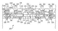
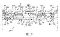
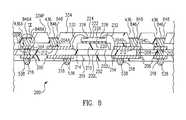
- stackable treated via package 200sometimes called an electronic component package, includes a substrate 202 including an upper, e.g., first, surface 202 U and an opposite lower, e.g., second, surface 202 L.
- Substrate 202is a dielectric material such as laminate, ceramic, printed circuit board material, or other dielectric material.
- upper surface 202 U of substrate 202are electrically conductive upper, e.g., first, traces 204 , e.g., formed of copper.
- lower surface 202 L of substrate 202are lower, e.g., second, traces 206 .
- Lower traces 206are electrically connected to upper traces 204 by electrically conductive vias 208 extending through substrate 202 between upper surface 202 U and lower surface 202 L.
- Stackable treated via package 200further includes an upper, e.g., first, solder mask 210 on upper surface 202 U that protects first portions of upper traces 204 while exposing second portions, e.g., terminals 212 and/or bond fingers 214 , of upper traces 204 .
- an upper, e.g., first, solder mask 210 on upper surface 202 Uthat protects first portions of upper traces 204 while exposing second portions, e.g., terminals 212 and/or bond fingers 214 , of upper traces 204 .
- Stackable treated via package 200further includes a lower, e.g., second, solder mask 216 on lower surface 202 L that protects first portions of lower traces 206 while exposing second portions, e.g., terminals 218 , of lower traces 206 .
- a lower, e.g., second, solder mask 216 on lower surface 202 Lthat protects first portions of lower traces 206 while exposing second portions, e.g., terminals 218 , of lower traces 206 .
- upper interconnection balls 220are attached to terminals 212 of upper traces 204 .
- upper interconnection balls 220are formed of solder.
- upper interconnection balls 220are formed of other electrically conductive material such as plated copper or electrically conductive adhesive. As illustrated, upper interconnection balls 220 are approximately spherical and the exposed upper surfaces of upper interconnection balls 220 are thus sometime called convex surfaces.
- attach electronic component operation 104an electronic component 222 is attached.
- electronic component 222is an integrated circuit chip, e.g., an active component. However, in other embodiments, electronic component 222 is a passive component such as a capacitor, resistor, or inductor. In another embodiment, electronic component 222 is a pre-packaged device. In yet another embodiment, a plurality of electronic components are mounted, e.g., in a stacked configuration.
- electronic component 222includes an active surface 224 and an opposite inactive surface 226 .
- Electronic component 222further includes bond pads 228 formed on active surface 224 .
- Inactive surface 226is mounted to upper solder mask 210 with an adhesive 230 , sometimes called a die attach adhesive.
- upper solder mask 210is patterned to expose a portion of upper surface 202 U of substrate 202 and inactive surface 226 is mounted to the exposed portion of upper surface 202 U of substrate 202 with adhesive 230 .
- electronic component 222is mounted to substrate 202 .
- wirebond operation 106bond pads 228 are electrically connected to upper traces 204 , e.g., bond fingers 214 thereof, by electrically conductive bond wires 232 .
- electronic component 222is illustrated and described as being mounted in a wirebond configuration, in other embodiments, electronic component 222 is mounted in a different configuration such as a flip chip configuration.
- flip chip bumpse.g., solder
- wirebond operation 106is optional, e.g., is not performed in the case when electronic component 222 is mounted in a flip chip configuration or other configuration not requiring bond wires 232 .
- electrically conductive pathway between bond pads 228 and lower traces 206is described above, other electrically conductive pathways can be formed.
- contact metallizationscan be formed between the various electrical conductors.
- one or more of upper traces 204is not electrically connected to lower traces 206 , i.e., is electrically isolated from lower traces 206 , and electrically connected to bond pads 228 .
- a first upper trace 204 A of the plurality of upper traces 204is electrically isolated from lower traces 206 and electrically connected to a respective bond pad 228 .
- the respective bond pad 228 electrically connected to upper trace 204 Ais also electrically isolated from lower traces 206 .
- one or more of upper traces 204is electrically connected to both bond pads 228 and to lower traces 206 .
- a second upper trace 204 B of the plurality of upper traces 204is electrically connected to lower trace(s) 206 by a via 208.
- the respective bond pad 228 electrically connected to upper trace 204 Bis also electrically connected to lower trace(s) 206 .
- one or more of upper traces 204is not electrically connected to a bond pad 228 , i.e., is electrically isolated from bond pads 228 , and is electrically connected to lower traces 206 .
- a third upper trace 204 Cis electrically isolated from bond pads 228 and electrically connected to lower trace(s) 206 .
- the respective lower trace(s) 206 electrically connected to upper trace 204 Care also electrically isolated from bond pads 228 .
- upper traces 204are electrically connected to lower traces 206 , to bond pads 228 , and/or to lower traces 206 and bond pads 228 .
- upper interconnection balls 220are electrically connected to lower traces 206 only, to bond pads 228 only, and/or to both lower traces 206 and bond pads 228 .
- connection between bond pads 228 , upper traces 204 , lower traces 206 , and upper interconnection balls 220are set forth above, in light of this disclosure, those of skill in the art will understand that any one of a number of electrical configurations are possible depending upon the particular application.
- FIG. 2Ais a cross-sectional view of a stackable treated via package 200 A during fabrication in accordance with another embodiment.
- Stackable treated via package 200 A of FIG. 2Ais similar to stackable treated via package 200 of FIG. 2 and only the significant differences are discussed below.
- electronic component 222is mounted in a flip chip configuration. More particularly, flip chip bumps 231 , e.g., solder, form the physical and electrical connections between bond pads 228 and upper traces 204 , e.g., bond fingers 214 thereof.
- flip chip bumps 231e.g., solder
- an underfill 233is applied between active surface 224 of electronic component 222 and upper solder mask 210 (or upper surface 202 U of substrate 202 ) and encloses and protects flip chip bumps 231 .
- attach electronic component operation 104is performed prior to attach upper interconnection balls operation 102 .
- electronic component 222is flip chip mounted with flip chip bumps 231 first and then upper interconnection balls 220 are attached to terminals 212 .
- wirebond operation 106is not performed and flow moves directly from attach upper interconnection balls operation 102 to an encapsulate operation 108 .
- attach electronic component operation 104is performed simultaneously with attach upper interconnection balls operation 102 .
- upper interconnection balls 220are attached to terminals 212 and electronic component 222 is flip chip mounted with flip chip bumps 231 simultaneously, e.g., in a single reflow operation.
- wirebond operation 106is not performed and flow moves directly from both attach upper interconnection balls operation 102 and attach electronic component operation 104 to encapsulate operation 108 .
- stackable treated via package 200 of FIG. 2is illustrated in the following figures, in light of this disclosure, those of skill in the art will understand that the operations can equally be performed with stackable treated via package 200 A of FIG. 2A .
- FIG. 3is a cross-sectional view of stackable treated via package 200 of FIG. 2 at a later stage during fabrication in accordance with one embodiment.
- encapsulate operation 108electronic component 222 , bond wires 232 , upper interconnection balls 220 , upper solder mask 210 and any exposed portions of upper surface 202 U and/or upper traces 204 are enclosed, sometimes called encased, encapsulated, and/or covered, with a package body 334 .
- package body 334is a cured liquid encapsulant, molding compound, or other dielectric material.
- Package body 334protects electronic component 222 , bond wires 232 , upper interconnection balls 220 , upper solder mask 210 and any exposed portions of upper surface 202 U and/or upper traces 204 from the ambient environment, e.g., from contact, moisture and/or shorting to other structures.
- Package body 334includes a principal surface 334 P parallel to upper surface 202 U of substrate 202 .
- principal surface 334 Pparallel to upper surface 202 U of substrate 202 .
- parallel, perpendicular, and similar termsare used herein, it is to be understood that the described features may not be exactly parallel and perpendicular, but only substantially parallel and perpendicular to within excepted manufacturing tolerances.
- FIG. 4is a cross-sectional view of stackable treated via package 200 of FIG. 3 at a later stage during fabrication in accordance with one embodiment. Referring now to FIGS. 1 and 4 together, from encapsulate operation 108 , flow moves to a form via apertures operation 110 . In form via apertures operation 110 , via apertures 436 are formed in package body 334 .
- Via apertures 436penetrate into package body 334 from principal surface 334 P to expose upper interconnection balls 220 .
- Each via aperture 436exposes a respective interconnection ball 220 on a respective terminal 212 .
- via aperture 436are formed using a laser-ablation process. More particularly, a laser is repeatedly directed at principal surface 334 P perpendicularly to principal surface 334 P. This laser ablates, i.e., removes, portions of package body 334 leaving via apertures 436 , sometimes called through holes.
- via apertures 436are formed using selective molding, milling, mechanical drilling, chemical etching and/or other via aperture formation techniques.
- a first via aperture 436 A of the plurality of via apertures 436extends between principal surface 334 P of package body 334 and a first upper interconnection ball 220 A of upper interconnection balls 220 . Accordingly, upper interconnection ball 220 A is exposed through via aperture 436 A.
- Via aperture 436 Atapers from principal surface 334 P to upper interconnection ball 220 A. More particularly, the diameter of via aperture 436 A in a plane parallel to principal surface 334 P is greatest at the top of via aperture 436 A, and smallest at the bottom of via aperture 436 A and gradually diminishes between the top and bottom of via aperture 436 A. The top of via aperture 436 A is located at principal surface 334 P and the bottom of via aperture 436 is located at upper interconnection ball 220 A in this embodiment.
- via aperture 436 Ahas a uniform diameter, i.e., has a cylindrical shape.
- via aperture 436 Atapers from the bottom to the top of via aperture 436 A. More particularly, the diameter of via aperture 436 A in a plane parallel to principal surface 334 P is smallest at the top of via aperture 436 A and greatest at the bottom of via aperture 436 A and gradually increases between the top and bottom of via aperture 436 A.
- via aperture 436 AAlthough only a single via aperture 436 A is described in detail, in light of this disclosure, those of skill in the art will understand that the description is equally applicable to all of via apertures 436 .
- FIG. 5is a cross-sectional view of stackable treated via package 200 of FIG. 4 at a later stage during fabrication in accordance with one embodiment.
- attach lower interconnection balls operation 112lower, e.g., second, interconnection balls 538 are attached to lower traces 206 , e.g., terminals 218 thereof.
- lower interconnection balls 538are formed of solder. In other embodiments, lower interconnection balls 538 are formed of other electrically conductive material such as plated copper or electrically conductive adhesive.
- attach lower interconnection balls operation 112is set forth at a particular stage during fabrication of stackable treated via package 200 , in other embodiments, attach lower interconnection balls operation 112 is performed at an earlier or later stage during fabrication of stackable treated via package 200 .
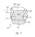
- treat upper interconnection balls operation 114upper interconnection balls 220 ( FIG. 5 ) are treated to form treated interconnection balls 640 as illustrated in FIGS. 6 and 7 .
- Treated interconnection balls 640include a first treated interconnection ball 640 A.
- treated interconnection balls 640include upper, e.g., first, flat surfaces 642 .
- treated interconnection ball 640 Aincludes a first flat surface 642 A of the plurality of flat surfaces 642 .
- Flat surfaces 642are sometimes called treated surfaces.
- a jigincludes a plurality of flat ended pins.
- the flat ended pinsare passed through via apertures 436 and pressed downward on upper interconnection balls 220 to simultaneously flatten all of upper interconnection balls 220 ( FIG. 5 ) to form treated interconnection balls 640 .
- stackable treated via package 200is formed simultaneously with a plurality of stackable treated via package 200 in an array or strip, e.g., a strip of four.
- a jig including a plurality of flat ended pins corresponding to upper interconnection balls 220is pressed downward on the array or strip to simultaneously flatten all of upper interconnection balls 220 of the array or strip to form treated interconnection balls 640 .
- the array or stripis singulated to form individual stackable treated via package 200 .
- treated interconnection balls 640include concave surfaces.
- stackable treated via package 200is warped, e.g., due to mismatch in stress generated by the various layers such as substrate 202 and package body 334 .
- Stackable treated via package 200is warped prior to performance of treat upper interconnection balls operation 114 .
- stackable treated via package 200is warped at the stage illustrated in FIG. 5 . Due to this warpage, upper interconnection balls 220 are not perfectly coplanar at the stage illustrated in FIG. 5 .
- upper interconnection balls 220are formed with a certain amount of tolerance and thus mismatch. Stated another way, some of upper interconnection balls 220 are larger than others of upper interconnection balls 220 . For example, upper interconnection balls 220 vary slightly in size at the stage illustrated in FIG. 5 . Due to this variation in size, upper interconnection balls 220 are not perfectly coplanar at the stage illustrated in FIG. 5 .
- upper interconnection balls 220are coplanar prior to performance of treat upper interconnection balls 114 .
- FIG. 8is a cross-sectional view of stackable treated via package 200 of FIG. 5 at a later stage during fabrication in accordance with another embodiment.
- FIG. 9Ais an enlarged cross-sectional view of the region IX of stackable treated via package 200 of FIG. 8 .
- Treated interconnection balls 846include upper, e.g., first, jagged surfaces 848 .
- interconnection ball 846 Aincludes a first jagged surface 848 A of jagged surfaces 848 .
- Jagged surfaces 848are sometimes called treated surfaces.
- a jigincludes a plurality of jagged ended pins.
- the jagged ended pinsare passed through via apertures 436 and pressed downward on upper interconnection balls 220 to simultaneously deform all of upper interconnection balls 220 ( FIG. 5 ) to form treated interconnection balls 846 .
- stackable treated via package 200is formed simultaneously with a plurality of stackable treated via package 200 in an array or strip, e.g., a strip of four.
- a jig including a plurality of jagged ended pins corresponding to upper interconnection balls 220is pressed downward on the array or strip to simultaneously deform all of upper interconnection balls 220 of the array or strip to form treated interconnection balls 846 .
- the array or stripis singulated to form individual stackable treated via package 200 .
- Jagged surfaces 848are sharply uneven surfaces, sometimes called roughened surfaces. Jagged surfaces 848 are exposed through via apertures 436 while the rest of treated interconnection balls 846 is enclosed within package body 334 .
- jagged surfaces 848are hatched to include one or more alternating repeating peaks 850 and valleys 852 . Peaks 850 jut out from (protrude from) treated interconnection balls 846 . In the opposite manner, valleys 852 are recessed within treated interconnection balls 846 . Jagged surfaces 848 are sometimes said to have projections which project from treated interconnection balls 846 .
- FIG. 9Bis a top plan view of treated interconnection ball 846 A of FIGS. 8 and 9A in accordance with one embodiment.
- jagged surface 848 A of treated interconnection ball 846 Ais hatched, sometimes called scratched or scored, with a series of parallel lines to form peaks 850 and valleys 852 . More particularly, peaks 850 and valleys 852 are parallel to one another and extend lengthwise in a direction parallel with upper surface 202 U of substrate 202 .
- FIG. 9Cis a top plan view of a treated interconnection ball 846 B in accordance with another embodiment.
- Treated interconnection ball 846 Bis similar to treated interconnection ball 846 A of FIGS. 8 and 9A and only the significant differences are discussed below.
- a jagged surface 848 B of treated interconnection ball 846 Bis cross-hatched, sometimes called scratched or scored, with a series of criss-cross (checkerboard) parallel lines 954 , 956 .
- jagged surfaces 848 A, 848 B of FIGS. 9B , 9 Cgenerally apply to all jagged surfaces 848 of stackable treated via package 200 of FIG. 8 depending upon the particular embodiment.
- jagged surfaces 848 A, 848 Bare provided in FIGS. 9B , 9 C, in light of this disclosure, those of skill in the art will understand that jagged surfaces 848 can be roughened with other patterns.
- jagged surfaces 848have a roughness (vertical deviations) greater than upper interconnection balls 220 ( FIG. 5 ).
- jagged surfaces 848break the oxide layer of interconnection balls of an upper electronic component package stacked upon stackable treated via package 200 thus enhancing bonding therewith and maximizing yield.
- the entire upper surfaces of treated interconnection balls 846are illustrated as jagged surfaces 848 , in other examples, only top portions of the upper surfaces of treated interconnection balls 846 are jagged and the remaining lower portions are convex and smooth.
- FIG. 10is a cross-sectional view of an electronic component assembly 1000 including stackable treated via package 200 of FIGS. 6 , 7 during fabrication in accordance with one embodiment.
- stackable via package 200is stacked on a larger substrate 1070 .
- Larger substrate 1070e.g., a printed circuit motherboard, includes a dielectric substrate 1072 having an upper, e.g., first, surface 1072 U and an opposite lower, e.g., second, surface 1072 L.
- Terminals 1074e.g., of a circuit pattern, are formed on upper surface 1072 U of substrate 1072 .
- Terminals 1074e.g., of a circuit pattern
- larger substrate 1070can have additional and/or difference circuit patterns depending upon the particular application.
- Larger substrate 1070further includes an upper, e.g., first, solder mask 1076 on upper surface 1072 U of substrate 1072 and a lower, e.g., second, solder mask 1078 on lower surface 1072 L of substrate 1072 .
- Upper solder mask 1076is patterned to expose terminal 1074 .
- Solder structures 1080are formed on terminals 1074 .
- solder structures 1080are formed of screen printed solder paste.
- Lower interconnection balls 538 of stackable treated via package 200are placed into contact (stacked on) respective solder structures 1080 .
- an upper, e.g., second, electronic component package 1082is stacked upon stackable treated via package 200 .
- Upper electronic component package 1082is sometimes called a stacked electronic component package.
- Upper electronic component package 1082includes a substrate 1002 , an upper surface 1002 U, a lower surface 1002 L, upper traces 1004 , lower traces 1006 , vias 1008 , an upper solder mask 1010 , bond fingers 1014 , a lower solder mask 1016 , terminals 1018 , an electronic component 1022 , an active surface 1024 , an inactive surface 1026 , bond pads 1028 , an adhesive 1030 , bond wires 1032 , a package body 1034 , and lower interconnection balls 1038 similar to substrate 202 , upper surface 202 U, lower surface 202 L, upper traces 204 , lower traces 206 , vias 208 , upper solder mask 210 , bond fingers 214 , lower solder mask 216 , terminals 218 , electronic component 222 , active surface 224 , inactive surface 226 , bond pads 228 , adhesive 230 , bond wires 232 , package body 334 , and lower interconnection balls 538 of
- Lower interconnection balls 1038 of upper electronic component package 1082are placed into via apertures 436 and upon flat surfaces 642 of treated interconnection balls 640 . As flat surfaces 642 lie in a flat seating plane as discussed above, contact between lower interconnection balls 1038 of upper electronic component package 1082 and treated interconnection balls 640 is enhanced thus enhancing bonding therebetween.
- lower interconnection balls 538 and/or lower interconnection balls 1038are flux dipped prior to stacking.
- an upper electronic component package 1082includes an electronic component mounted in a flip chip configuration and/or multiple electronic components stacked one upon another or side by side.
- FIG. 11is a cross-sectional view of electronic component assembly 1000 of FIG. 10 at a later stage during fabrication in accordance with one embodiment.
- assembly 1000is heated to reflow, i.e., melt and resolidify, lower interconnection balls 1038 , treated interconnection balls 640 , lower interconnection balls 538 , and solder structures 1080 .
- lower interconnection balls 1038 and treated interconnection balls 640are heated to melt lower interconnection balls 1038 and treated interconnection balls 640 .
- lower interconnection balls 1038 and treated interconnection balls 640combine (intermix) into molten structures, e.g., molten solder.
- treated interconnection balls 640dome up enhancing intermixing of lower interconnection balls 1038 and treated interconnection balls 640 to form the molten structures.
- solder columns 1184are integral, i.e., are single unitary structures and not a plurality of different layers connected together.
- Solder columns 1184extend through via apertures 436 and between lower terminals 1018 of upper electronic component package 1082 and terminals 212 of stackable treated via package 200 .
- upper electronic component package 1082is mounted and electrically connected to stackable treated via package 200 by solder columns 1184 .
- lower interconnection balls 538 and solder structures 1080e.g., solder
- lower interconnection balls 538 and solder structures 1080are heated to melt lower interconnection balls 538 and solder structures 1080 .
- lower interconnection balls 538 and solder structures 1080combine (intermix) into molten structures, e.g., molten solder.
- molten structurescool and form solder columns 1186 .
- solder columns 1186are integral, i.e., are single unitary structures and not a plurality of different layers connected together.
- Solder columns 1186extend between lower terminals 218 of stackable treated via package 200 and terminals 1074 of larger substrate 1070 .
- stackable treated via package 200is mounted and electrically connected to larger substrate 1070 by solder columns 1186 .
- electronic component assembly 1000 including treated interconnection balls 640is illustrated in FIG. 10
- electronic component assembly 1000includes treated interconnection balls 846 of FIG. 8 instead of treated interconnection balls 640 .
- lower interconnection balls 1038 of upper electronic component package 1082are placed into via apertures 436 and upon jagged surfaces 848 of treated interconnection balls 846 .
- treated interconnection balls 846break the oxide layer of lower interconnection balls 1038 of upper electronic component package 1082 thus enhancing bonding therewith. More particularly, lower interconnection balls 1038 and treated interconnection balls 846 , e.g., solder, are heated to melt lower interconnection balls 1038 and treated interconnection balls 846 . Upon melting, lower interconnection balls 1038 and treated interconnection balls 846 combine (intermix) into molten structures, e.g., molten solder. During melting, jagged surface 848 break the oxide layer of lower interconnection balls 1038 enhancing intermixing of lower interconnection balls 1038 and treated interconnection balls 846 to form the molten structures. These molten structures cool and form solder columns 1184 .
- molten structurescool and form solder columns 1184 .
Landscapes
- Engineering & Computer Science (AREA)
- Power Engineering (AREA)
- Microelectronics & Electronic Packaging (AREA)
- Physics & Mathematics (AREA)
- Condensed Matter Physics & Semiconductors (AREA)
- General Physics & Mathematics (AREA)
- Computer Hardware Design (AREA)
- Electric Connection Of Electric Components To Printed Circuits (AREA)
Abstract
Description
Claims (19)
Priority Applications (1)
| Application Number | Priority Date | Filing Date | Title |
|---|---|---|---|
| US12/787,238US8300423B1 (en) | 2010-05-25 | 2010-05-25 | Stackable treated via package and method |
Applications Claiming Priority (1)
| Application Number | Priority Date | Filing Date | Title |
|---|---|---|---|
| US12/787,238US8300423B1 (en) | 2010-05-25 | 2010-05-25 | Stackable treated via package and method |
Publications (1)
| Publication Number | Publication Date |
|---|---|
| US8300423B1true US8300423B1 (en) | 2012-10-30 |
Family
ID=47045789
Family Applications (1)
| Application Number | Title | Priority Date | Filing Date |
|---|---|---|---|
| US12/787,238Active2031-01-14US8300423B1 (en) | 2010-05-25 | 2010-05-25 | Stackable treated via package and method |
Country Status (1)
| Country | Link |
|---|---|
| US (1) | US8300423B1 (en) |
Cited By (10)
| Publication number | Priority date | Publication date | Assignee | Title |
|---|---|---|---|---|
| US20090184412A1 (en)* | 2007-10-25 | 2009-07-23 | Rohm Co., Ltd. | Resin-seal type semiconductor device |
| US8482134B1 (en)* | 2010-11-01 | 2013-07-09 | Amkor Technology, Inc. | Stackable package and method |
| US8890337B1 (en) | 2011-09-20 | 2014-11-18 | Amkor Technology, Inc. | Column and stacking balls package fabrication method and structure |
| US9177932B1 (en)* | 2010-12-03 | 2015-11-03 | Amkor Technology, Inc. | Semiconductor device having overlapped via apertures |
| US9263412B2 (en) | 2012-03-09 | 2016-02-16 | Taiwan Semiconductor Manufacturing Company, Ltd. | Packaging methods and packaged semiconductor devices |
| US9269687B2 (en) | 2012-03-09 | 2016-02-23 | Taiwan Semiconductor Manufacturing Company, Ltd. | Packaging methods and packaged semiconductor devices |
| US20160284654A1 (en)* | 2013-03-15 | 2016-09-29 | Taiwan Semiconductor Manufacturing Company, Ltd. | Fan-Out Interconnect Structure and Method for Forming Same |
| US9673178B2 (en) | 2015-10-15 | 2017-06-06 | Powertech Technology Inc. | Method of forming package structure with dummy pads for bonding |
| US20170294776A1 (en)* | 2016-04-11 | 2017-10-12 | Zf Friedrichshafen Ag | Electronic unit comprising an esd protective arrangement |
| US10629476B2 (en)* | 2014-03-12 | 2020-04-21 | Taiwan Semiconductor Manufacturing Company, Ltd. | Packages with through-vias having tapered ends |
Citations (169)
| Publication number | Priority date | Publication date | Assignee | Title |
|---|---|---|---|---|
| US3868724A (en) | 1973-11-21 | 1975-02-25 | Fairchild Camera Instr Co | Multi-layer connecting structures for packaging semiconductor devices mounted on a flexible carrier |
| US3916434A (en) | 1972-11-30 | 1975-10-28 | Power Hybrids Inc | Hermetically sealed encapsulation of semiconductor devices |
| US4322778A (en) | 1980-01-25 | 1982-03-30 | International Business Machines Corp. | High performance semiconductor package assembly |
| US4532419A (en) | 1982-09-09 | 1985-07-30 | Sony Corporation | Memory card having static electricity protection |
| US4642160A (en) | 1985-08-12 | 1987-02-10 | Interconnect Technology Inc. | Multilayer circuit board manufacturing |
| US4645552A (en) | 1984-11-19 | 1987-02-24 | Hughes Aircraft Company | Process for fabricating dimensionally stable interconnect boards |
| US4685033A (en) | 1984-08-28 | 1987-08-04 | Nec Corporation | Multilayer wiring substrate |
| US4706167A (en) | 1983-11-10 | 1987-11-10 | Telemark Co., Inc. | Circuit wiring disposed on solder mask coating |
| US4716049A (en) | 1985-12-20 | 1987-12-29 | Hughes Aircraft Company | Compressive pedestal for microminiature connections |
| US4786952A (en) | 1986-07-24 | 1988-11-22 | General Motors Corporation | High voltage depletion mode MOS power field effect transistor |
| US4806188A (en) | 1988-03-04 | 1989-02-21 | E. I. Du Pont De Nemours And Company | Method for fabricating multilayer circuits |
| US4811082A (en) | 1986-11-12 | 1989-03-07 | International Business Machines Corporation | High performance integrated circuit packaging structure |
| US4897338A (en) | 1987-08-03 | 1990-01-30 | Allied-Signal Inc. | Method for the manufacture of multilayer printed circuit boards |
| US4905124A (en) | 1987-03-31 | 1990-02-27 | Mitsubishi Denki Kabushiki Kaisha | IC card |
| US4964212A (en) | 1988-09-29 | 1990-10-23 | Commissariat A L'energie Atomique | Process for producing electrical connections through a substrate |
| US4974120A (en) | 1989-01-12 | 1990-11-27 | Mitsubishi Denki Kabushiki Kaisha | IC card |
| US4996391A (en) | 1988-09-30 | 1991-02-26 | Siemens Aktiengesellschaft | Printed circuit board having an injection molded substrate |
| US5021047A (en) | 1989-08-29 | 1991-06-04 | Movern John B | Restricted use hypodermic syringe |
| US5072075A (en) | 1989-06-28 | 1991-12-10 | Digital Equipment Corporation | Double-sided hybrid high density circuit board and method of making same |
| US5072520A (en) | 1990-10-23 | 1991-12-17 | Rogers Corporation | Method of manufacturing an interconnect device having coplanar contact bumps |
| US5081520A (en) | 1989-05-16 | 1992-01-14 | Minolta Camera Kabushiki Kaisha | Chip mounting substrate having an integral molded projection and conductive pattern |
| US5091769A (en) | 1991-03-27 | 1992-02-25 | Eichelberger Charles W | Configuration for testing and burn-in of integrated circuit chips |
| US5108553A (en) | 1989-04-04 | 1992-04-28 | Olin Corporation | G-tab manufacturing process and the product produced thereby |
| US5110664A (en) | 1989-07-10 | 1992-05-05 | Hitachi, Ltd. | Thick film and thin film composite substrate and electronic circuit apparatus using it |
| US5191174A (en) | 1990-08-01 | 1993-03-02 | International Business Machines Corporation | High density circuit board and method of making same |
| US5229550A (en) | 1990-10-30 | 1993-07-20 | International Business Machines Corporation | Encapsulated circuitized power core alignment and lamination |
| US5239448A (en) | 1991-10-28 | 1993-08-24 | International Business Machines Corporation | Formulation of multichip modules |
| US5247429A (en) | 1990-11-21 | 1993-09-21 | Nippondenso Co., Ltd. | Display board |
| US5250843A (en) | 1991-03-27 | 1993-10-05 | Integrated System Assemblies Corp. | Multichip integrated circuit modules |
| US5278726A (en) | 1992-01-22 | 1994-01-11 | Motorola, Inc. | Method and apparatus for partially overmolded integrated circuit package |
| US5283459A (en) | 1989-11-15 | 1994-02-01 | Kabushiki Kaisha Toshiba | Semiconductor sensor including an aperture having a funnel shaped section intersecting a second section |
| US5353498A (en) | 1993-02-08 | 1994-10-11 | General Electric Company | Method for fabricating an integrated circuit module |
| US5371654A (en) | 1992-10-19 | 1994-12-06 | International Business Machines Corporation | Three dimensional high performance interconnection package |
| US5379191A (en) | 1991-02-26 | 1995-01-03 | Microelectronics And Computer Technology Corporation | Compact adapter package providing peripheral to area translation for an integrated circuit chip |
| US5404044A (en) | 1992-09-29 | 1995-04-04 | International Business Machines Corporation | Parallel process interposer (PPI) |
| US5463253A (en) | 1990-03-15 | 1995-10-31 | Fujitsu Limited | Semiconductor device having a plurality of chips |
| US5474957A (en) | 1994-05-09 | 1995-12-12 | Nec Corporation | Process of mounting tape automated bonded semiconductor chip on printed circuit board through bumps |
| US5474958A (en) | 1993-05-04 | 1995-12-12 | Motorola, Inc. | Method for making semiconductor device having no die supporting surface |
| US5508938A (en) | 1992-08-13 | 1996-04-16 | Fujitsu Limited | Special interconnect layer employing offset trace layout for advanced multi-chip module packages |
| US5530288A (en) | 1994-10-12 | 1996-06-25 | International Business Machines Corporation | Passive interposer including at least one passive electronic component |
| US5531020A (en) | 1989-11-14 | 1996-07-02 | Poly Flex Circuits, Inc. | Method of making subsurface electronic circuits |
| US5546654A (en) | 1994-08-29 | 1996-08-20 | General Electric Company | Vacuum fixture and method for fabricating electronic assemblies |
| US5574309A (en) | 1991-11-25 | 1996-11-12 | Gemplus Card International | Integrated circuit card comprising means for the protection of the integrated circuit |
| US5578934A (en)* | 1991-06-04 | 1996-11-26 | Micron Technology, Inc. | Method and apparatus for testing unpackaged semiconductor dice |
| US5581498A (en) | 1993-08-13 | 1996-12-03 | Irvine Sensors Corporation | Stack of IC chips in lieu of single IC chip |
| US5582858A (en) | 1991-10-07 | 1996-12-10 | International Business Machines Corporation | Adhesive layer in multi-level packaging and organic material as a metal diffusion barrier |
| US5616422A (en) | 1994-02-28 | 1997-04-01 | International Business Machines Corporation | Metallized substrate |
| US5637832A (en) | 1993-10-26 | 1997-06-10 | Pacific Microelectronics Corporation | Solder ball array and method of preparation |
| US5674785A (en) | 1995-11-27 | 1997-10-07 | Micron Technology, Inc. | Method of producing a single piece package for semiconductor die |
| US5719749A (en) | 1994-09-26 | 1998-02-17 | Sheldahl, Inc. | Printed circuit assembly with fine pitch flexible printed circuit overlay mounted to printed circuit board |
| US5721496A (en)* | 1996-01-23 | 1998-02-24 | Micron Technology, Inc. | Method and apparatus for leak checking unpackaged semiconductor dice |
| US5726493A (en) | 1994-06-13 | 1998-03-10 | Fujitsu Limited | Semiconductor device and semiconductor device unit having ball-grid-array type package structure |
| US5739581A (en) | 1995-11-17 | 1998-04-14 | National Semiconductor Corporation | High density integrated circuit package assembly with a heatsink between stacked dies |
| US5739588A (en) | 1994-08-15 | 1998-04-14 | Citizen Watch Co., Ltd. | Semiconductor device |
| US5742479A (en) | 1994-03-09 | 1998-04-21 | Seiko Epson Corporation | Card-type electronic device with plastic frame sandwiched between printed circuit board and metal panel |
| US5774340A (en) | 1996-08-28 | 1998-06-30 | International Business Machines Corporation | Planar redistribution structure and printed wiring device |
| US5798014A (en) | 1995-02-02 | 1998-08-25 | Hestia Technologies, Inc. | Methods of making multi-tier laminate substrates for electronic device packaging |
| US5822190A (en) | 1996-06-11 | 1998-10-13 | Kabushiki Kaisha Toshiba | Card type memory device and a method for manufacturing the same |
| US5826330A (en) | 1995-12-28 | 1998-10-27 | Hitachi Aic Inc. | Method of manufacturing multilayer printed wiring board |
| US5835355A (en) | 1997-09-22 | 1998-11-10 | Lsi Logic Corporation | Tape ball grid array package with perforated metal stiffener |
| US5847453A (en) | 1996-03-27 | 1998-12-08 | Honda Giken Kogyo Kabushiki Kaisha | Microwave circuit package |
| US5883425A (en) | 1995-10-27 | 1999-03-16 | Mitsubishi Denki Kabushiki Kaisha | Circuit device |
| US5894108A (en) | 1997-02-11 | 1999-04-13 | National Semiconductor Corporation | Plastic package with exposed die |
| US5903052A (en) | 1998-05-12 | 1999-05-11 | Industrial Technology Research Institute | Structure for semiconductor package for improving the efficiency of spreading heat |
| US5907477A (en) | 1995-09-19 | 1999-05-25 | Micron Communications, Inc. | Substrate assembly including a compartmental dam for use in the manufacturing of an enclosed electrical circuit using an encapsulant |
| US5915977A (en)* | 1997-06-02 | 1999-06-29 | Micron Technology, Inc. | System and interconnect for making temporary electrical connections with bumped semiconductor components |
| US5924003A (en) | 1997-11-14 | 1999-07-13 | Kinetrix, Inc. | Method of manufacturing ball grid arrays for improved testability |
| US5936843A (en) | 1997-10-14 | 1999-08-10 | Fujitsu Limited | Printed wiring board with mounted circuit element using a terminal density conversion board |
| US5952611A (en) | 1997-12-19 | 1999-09-14 | Texas Instruments Incorporated | Flexible pin location integrated circuit package |
| US6004619A (en) | 1996-11-07 | 1999-12-21 | Hewlett-Packard Company | Process for manufacturing printed circuit boards |
| US6013948A (en) | 1995-11-27 | 2000-01-11 | Micron Technology, Inc. | Stackable chip scale semiconductor package with mating contacts on opposed surfaces |
| US6021564A (en) | 1996-11-08 | 2000-02-08 | W. L. Gore & Associates, Inc. | Method for reducing via inductance in an electronic assembly and article |
| US6028364A (en) | 1994-09-20 | 2000-02-22 | Hitachi, Ltd. | Semiconductor device having a stress relieving mechanism |
| US6034427A (en) | 1998-01-28 | 2000-03-07 | Prolinx Labs Corporation | Ball grid array structure and method for packaging an integrated circuit chip |
| US6035527A (en) | 1996-05-18 | 2000-03-14 | Ingenieurbuero Tamm Factory Innovations | Method for the production of printed circuit boards |
| US6040239A (en)* | 1997-08-22 | 2000-03-21 | Micron Technology, Inc. | Non-oxidizing touch contact interconnect for semiconductor test systems and method of fabrication |
| US6040622A (en) | 1998-06-11 | 2000-03-21 | Sandisk Corporation | Semiconductor package using terminals formed on a conductive layer of a circuit board |
| US6060778A (en) | 1997-05-17 | 2000-05-09 | Hyundai Electronics Industries Co. Ltd. | Ball grid array package |
| US6069407A (en) | 1998-11-18 | 2000-05-30 | Vlsi Technology, Inc. | BGA package using PCB and tape in a die-up configuration |
| US6072243A (en) | 1996-11-26 | 2000-06-06 | Sharp Kabushiki Kaisha | Semiconductor integrated circuit device capable of surely electrically insulating two semiconductor chips from each other and fabricating method thereof |
| US6081036A (en) | 1996-04-19 | 2000-06-27 | Matsushita Electronics Corp. | Semiconductor device |
| US6122171A (en) | 1999-07-30 | 2000-09-19 | Micron Technology, Inc. | Heat sink chip package and method of making |
| US6119338A (en) | 1998-03-19 | 2000-09-19 | Industrial Technology Research Institute | Method for manufacturing high-density multilayer printed circuit boards |
| US6127833A (en) | 1999-01-04 | 2000-10-03 | Taiwan Semiconductor Manufacturing Co. | Test carrier for attaching a semiconductor device |
| US6160705A (en) | 1997-05-09 | 2000-12-12 | Texas Instruments Incorporated | Ball grid array package and method using enhanced power and ground distribution circuitry |
| US6172419B1 (en) | 1998-02-24 | 2001-01-09 | Micron Technology, Inc. | Low profile ball grid array package |
| US6175087B1 (en) | 1998-12-02 | 2001-01-16 | International Business Machines Corporation | Composite laminate circuit structure and method of forming the same |
| US6184463B1 (en) | 1998-04-13 | 2001-02-06 | Harris Corporation | Integrated circuit package for flip chip |
| US6194250B1 (en) | 1998-09-14 | 2001-02-27 | Motorola, Inc. | Low-profile microelectronic package |
| US6204453B1 (en) | 1998-12-02 | 2001-03-20 | International Business Machines Corporation | Two signal one power plane circuit board |
| US6214641B1 (en) | 1996-06-25 | 2001-04-10 | Micron Technology, Inc. | Method of fabricating a multi-chip module |
| US6239485B1 (en) | 1998-11-13 | 2001-05-29 | Fujitsu Limited | Reduced cross-talk noise high density signal interposer with power and ground wrap |
| USD445096S1 (en) | 1998-04-01 | 2001-07-17 | Sandisk Corporation | Removable memory card for use with portable electronic devices |
| US6274821B1 (en) | 1998-09-16 | 2001-08-14 | Denso Corporation | Shock-resistive printed circuit board and electronic device including the same |
| USD446525S1 (en) | 1999-08-24 | 2001-08-14 | Kabushiki Kaisha Toshiba | IC memory card |
| US6280641B1 (en) | 1998-06-02 | 2001-08-28 | Mitsubishi Gas Chemical Company, Inc. | Printed wiring board having highly reliably via hole and process for forming via hole |
| US6316285B1 (en) | 1998-09-02 | 2001-11-13 | Micron Technology, Inc. | Passivation layer for packaged integrated circuits |
| US20020017712A1 (en) | 1998-06-04 | 2002-02-14 | Yoshihiro Bessho | Method for fabricating a semiconductor package with a semiconductor device attached to a multilayered substrate |
| US6351031B1 (en) | 1999-10-12 | 2002-02-26 | Fujitsu Limited | Semiconductor device and method for manufacturing substrate of the same |
| US6353999B1 (en) | 1999-03-09 | 2002-03-12 | Unimicron Taiwan Corp. | Method of making mechanical-laser structure |
| US6365975B1 (en) | 1997-04-02 | 2002-04-02 | Tessera, Inc. | Chip with internal signal routing in external element |
| US6376906B1 (en) | 1997-02-12 | 2002-04-23 | Denso Corporation | Mounting structure of semiconductor element |
| US6392160B1 (en) | 1998-11-25 | 2002-05-21 | Lucent Technologies Inc. | Backplane for radio frequency signals |
| US20020061642A1 (en) | 1999-09-02 | 2002-05-23 | Matsushita Electric Industrial Co., Ltd. | Semiconductor device and method of manufacturing the same |
| US6395578B1 (en) | 1999-05-20 | 2002-05-28 | Amkor Technology, Inc. | Semiconductor package and method for fabricating the same |
| US20020066952A1 (en) | 2000-12-04 | 2002-06-06 | Fujitsu Limited | Semiconductor device having an interconnecting post formed on an interposer within a sealing resin |
| US6407930B1 (en) | 1999-06-23 | 2002-06-18 | Asustek Computer Inc. | Structure of printed circuit board with stacked daughter board |
| US6405431B1 (en) | 1996-06-27 | 2002-06-18 | Samsung Electro-Mechanics Co., Ltd. | Method for manufacturing build-up multi-layer printed circuit board by using yag laser |
| US6407341B1 (en) | 2000-04-25 | 2002-06-18 | International Business Machines Corporation | Conductive substructures of a multilayered laminate |
| US6406942B2 (en) | 2000-03-09 | 2002-06-18 | Nec Corporation | Flip chip type semiconductor device and method for manufacturing the same |
| US6448510B1 (en) | 1997-05-20 | 2002-09-10 | Micro Components Ltd. | Substrate for electronic packaging, pin jig fixture |
| US6479762B2 (en) | 2000-11-20 | 2002-11-12 | Alps Electric Co., Ltd. | Printed circuit board having a pattern of traces formed by screen-printing |
| US6497943B1 (en) | 2000-02-14 | 2002-12-24 | International Business Machines Corporation | Surface metal balancing to reduce chip carrier flexing |
| US20020195697A1 (en) | 2001-06-21 | 2002-12-26 | Mess Leonard E. | Stacked mass storage flash memory package |
| US20030025199A1 (en) | 2001-08-01 | 2003-02-06 | Chi-Chuan Wu | Super low profile package with stacked dies |
| US6517995B1 (en) | 1999-09-14 | 2003-02-11 | Massachusetts Institute Of Technology | Fabrication of finely featured devices by liquid embossing |
| US6534391B1 (en) | 2001-08-17 | 2003-03-18 | Amkor Technology, Inc. | Semiconductor package having substrate with laser-formed aperture through solder mask layer |
| US6544638B2 (en) | 1996-11-08 | 2003-04-08 | Gore Enterprise Holdings, Inc. | Electronic chip package |
| US6544461B1 (en)* | 1998-08-28 | 2003-04-08 | Micron Technology, Inc. | Test carrier with molded interconnect for testing semiconductor components |
| US6586682B2 (en) | 2000-02-23 | 2003-07-01 | Kulicke & Soffa Holdings, Inc. | Printed wiring board with controlled line impedance |
| US20030128096A1 (en) | 2002-01-10 | 2003-07-10 | Joseph Mazzochette | Temperature compensating device with integral sheet thermistors |
| US20030141582A1 (en) | 2002-01-25 | 2003-07-31 | Yang Chaur-Chin | Stack type flip-chip package |
| US6608757B1 (en) | 2002-03-18 | 2003-08-19 | International Business Machines Corporation | Method for making a printed wiring board |
| US20030197284A1 (en) | 2002-02-21 | 2003-10-23 | United Test & Assembly Center Limited | Semiconductor package |
| US6660559B1 (en) | 2001-06-25 | 2003-12-09 | Amkor Technology, Inc. | Method of making a chip carrier package using laser ablation |
| US20040063246A1 (en) | 2002-09-17 | 2004-04-01 | Chippac, Inc. | Semiconductor multi-package module having package stacked over die-down flip chip ball grid array package and having wire bond interconnect between stacked packages |
| US6715204B1 (en) | 1998-07-08 | 2004-04-06 | Ibiden Co., Ltd. | Printed wiring board and method for producing the same |
| US6727645B2 (en) | 2002-05-24 | 2004-04-27 | International Business Machines Corporation | Organic LED device |
| US6730857B2 (en) | 2001-03-13 | 2004-05-04 | International Business Machines Corporation | Structure having laser ablated features and method of fabricating |
| US6734542B2 (en) | 2000-12-27 | 2004-05-11 | Matsushita Electric Industrial Co., Ltd. | Component built-in module and method for producing the same |
| US6740964B2 (en) | 2000-11-17 | 2004-05-25 | Oki Electric Industry Co., Ltd. | Semiconductor package for three-dimensional mounting, fabrication method thereof, and semiconductor device |
| US6753612B2 (en) | 2001-04-05 | 2004-06-22 | International Business Machines Corporation | Economical high density chip carrier |
| US20040145044A1 (en) | 2002-01-23 | 2004-07-29 | Matsushita Electric Industrial Co., Ltd. | Circuit component built-in module with embedded semiconductor chip and method of manufacturing |
| US6774748B1 (en) | 1999-11-15 | 2004-08-10 | Nec Corporation | RF package with multi-layer substrate having coplanar feed through and connection interface |
| US20040159462A1 (en) | 1999-06-01 | 2004-08-19 | Chung Kevin Kwong-Tai | Flexible dielectric electronic substrate and method for making same |
| US6787443B1 (en) | 2003-05-20 | 2004-09-07 | Intel Corporation | PCB design and method for providing vented blind vias |
| US6803528B1 (en) | 1999-11-05 | 2004-10-12 | 3M Innovative Properties Company | Multi-layer double-sided wiring board and method of fabricating the same |
| US6815709B2 (en) | 2001-05-23 | 2004-11-09 | International Business Machines Corporation | Structure having flush circuitry features and method of making |
| US6815739B2 (en) | 2001-05-18 | 2004-11-09 | Corporation For National Research Initiatives | Radio frequency microelectromechanical systems (MEMS) devices on low-temperature co-fired ceramic (LTCC) substrates |
| US6838776B2 (en) | 2003-04-18 | 2005-01-04 | Freescale Semiconductor, Inc. | Circuit device with at least partial packaging and method for forming |
| US6888240B2 (en) | 2001-04-30 | 2005-05-03 | Intel Corporation | High performance, low cost microelectronic circuit package with interposer |
| US20050139985A1 (en) | 2003-12-25 | 2005-06-30 | Norio Takahashi | Semiconductor chip package and multichip package |
| US6921975B2 (en) | 2003-04-18 | 2005-07-26 | Freescale Semiconductor, Inc. | Circuit device with at least partial packaging, exposed active surface and a voltage reference plane |
| US6921968B2 (en) | 2003-05-02 | 2005-07-26 | Advance Semiconductor Engineering, Inc. | Stacked flip chip package |
| US6931726B2 (en) | 2001-10-16 | 2005-08-23 | International Business Machines Corporation | Method of making and interconnect structure |
| US6953995B2 (en) | 1996-03-12 | 2005-10-11 | Micron Technology, Inc. | Hermetic chip in wafer form |
| US20050242425A1 (en) | 2004-04-30 | 2005-11-03 | Leal George R | Semiconductor device with a protected active die region and method therefor |
| US6987314B1 (en) | 2004-06-08 | 2006-01-17 | Amkor Technology, Inc. | Stackable semiconductor package with solder on pads on which second semiconductor package is stacked |
| US7015075B2 (en) | 2004-02-09 | 2006-03-21 | Freescale Semiconuctor, Inc. | Die encapsulation using a porous carrier |
| US7030469B2 (en) | 2003-09-25 | 2006-04-18 | Freescale Semiconductor, Inc. | Method of forming a semiconductor package and structure thereof |
| US7081661B2 (en) | 2001-03-16 | 2006-07-25 | Matsushita Electric Industrial Co., Ltd. | High-frequency module and method for manufacturing the same |
| US7129113B1 (en)* | 2000-10-13 | 2006-10-31 | Bridge Semiconductor Corporation | Method of making a three-dimensional stacked semiconductor package with a metal pillar in an encapsulant aperture |
| US7185426B1 (en) | 2002-05-01 | 2007-03-06 | Amkor Technology, Inc. | Method of manufacturing a semiconductor package |
| US7198980B2 (en) | 2002-06-27 | 2007-04-03 | Micron Technology, Inc. | Methods for assembling multiple semiconductor devices |
| US7242081B1 (en) | 2006-04-24 | 2007-07-10 | Advanced Semiconductor Engineering Inc. | Stacked package structure |
| US7282394B2 (en) | 2004-12-30 | 2007-10-16 | Samsung Electro-Mechanics Co., Ltd. | Printed circuit board including embedded chips and method of fabricating the same using plating |
| US7285855B2 (en) | 2004-10-23 | 2007-10-23 | Freescale Semiconductor, Inc | Packaged device and method of forming same |
| US20070273049A1 (en) | 2006-05-12 | 2007-11-29 | Broadcom Corporation | Interconnect structure and formation for package stacking of molded plastic area array package |
| US20070281471A1 (en) | 2006-06-01 | 2007-12-06 | Dror Hurwitz | Advanced Multilayered Coreless Support Structures and their Fabrication |
| US20070290376A1 (en) | 2006-06-20 | 2007-12-20 | Broadcom Corporation | Integrated circuit (IC) package stacking and IC packages formed by same |
| US7345361B2 (en) | 2003-12-04 | 2008-03-18 | Intel Corporation | Stackable integrated circuit packaging |
| US7372151B1 (en) | 2003-09-12 | 2008-05-13 | Asat Ltd. | Ball grid array package and process for manufacturing same |
| US20080230887A1 (en) | 2007-03-23 | 2008-09-25 | Advanced Semiconductor Engineering, Inc. | Semiconductor package and the method of making the same |
| US7429786B2 (en) | 2005-04-29 | 2008-09-30 | Stats Chippac Ltd. | Semiconductor package including second substrate and having exposed substrate surfaces on upper and lower sides |
| US7459202B2 (en) | 2006-07-03 | 2008-12-02 | Motorola, Inc. | Printed circuit board |
| US7548430B1 (en) | 2002-05-01 | 2009-06-16 | Amkor Technology, Inc. | Buildup dielectric and metallization process and semiconductor package |
| US7550857B1 (en) | 2006-11-16 | 2009-06-23 | Amkor Technology, Inc. | Stacked redistribution layer (RDL) die assembly package |
| US7633765B1 (en) | 2004-03-23 | 2009-12-15 | Amkor Technology, Inc. | Semiconductor package including a top-surface metal layer for implementing circuit features |
| US7777351B1 (en) | 2007-10-01 | 2010-08-17 | Amkor Technology, Inc. | Thin stacked interposer package |
- 2010
- 2010-05-25USUS12/787,238patent/US8300423B1/enactiveActive
Patent Citations (177)
| Publication number | Priority date | Publication date | Assignee | Title |
|---|---|---|---|---|
| US3916434A (en) | 1972-11-30 | 1975-10-28 | Power Hybrids Inc | Hermetically sealed encapsulation of semiconductor devices |
| US3868724A (en) | 1973-11-21 | 1975-02-25 | Fairchild Camera Instr Co | Multi-layer connecting structures for packaging semiconductor devices mounted on a flexible carrier |
| US4322778A (en) | 1980-01-25 | 1982-03-30 | International Business Machines Corp. | High performance semiconductor package assembly |
| US4532419A (en) | 1982-09-09 | 1985-07-30 | Sony Corporation | Memory card having static electricity protection |
| US4706167A (en) | 1983-11-10 | 1987-11-10 | Telemark Co., Inc. | Circuit wiring disposed on solder mask coating |
| US4685033A (en) | 1984-08-28 | 1987-08-04 | Nec Corporation | Multilayer wiring substrate |
| US4645552A (en) | 1984-11-19 | 1987-02-24 | Hughes Aircraft Company | Process for fabricating dimensionally stable interconnect boards |
| US4642160A (en) | 1985-08-12 | 1987-02-10 | Interconnect Technology Inc. | Multilayer circuit board manufacturing |
| US4716049A (en) | 1985-12-20 | 1987-12-29 | Hughes Aircraft Company | Compressive pedestal for microminiature connections |
| US4786952A (en) | 1986-07-24 | 1988-11-22 | General Motors Corporation | High voltage depletion mode MOS power field effect transistor |
| US4811082A (en) | 1986-11-12 | 1989-03-07 | International Business Machines Corporation | High performance integrated circuit packaging structure |
| US4905124A (en) | 1987-03-31 | 1990-02-27 | Mitsubishi Denki Kabushiki Kaisha | IC card |
| US4897338A (en) | 1987-08-03 | 1990-01-30 | Allied-Signal Inc. | Method for the manufacture of multilayer printed circuit boards |
| US4806188A (en) | 1988-03-04 | 1989-02-21 | E. I. Du Pont De Nemours And Company | Method for fabricating multilayer circuits |
| US4964212A (en) | 1988-09-29 | 1990-10-23 | Commissariat A L'energie Atomique | Process for producing electrical connections through a substrate |
| US4996391A (en) | 1988-09-30 | 1991-02-26 | Siemens Aktiengesellschaft | Printed circuit board having an injection molded substrate |
| US4974120A (en) | 1989-01-12 | 1990-11-27 | Mitsubishi Denki Kabushiki Kaisha | IC card |
| US5108553A (en) | 1989-04-04 | 1992-04-28 | Olin Corporation | G-tab manufacturing process and the product produced thereby |
| US5081520A (en) | 1989-05-16 | 1992-01-14 | Minolta Camera Kabushiki Kaisha | Chip mounting substrate having an integral molded projection and conductive pattern |
| US5072075A (en) | 1989-06-28 | 1991-12-10 | Digital Equipment Corporation | Double-sided hybrid high density circuit board and method of making same |
| US5110664A (en) | 1989-07-10 | 1992-05-05 | Hitachi, Ltd. | Thick film and thin film composite substrate and electronic circuit apparatus using it |
| US5021047A (en) | 1989-08-29 | 1991-06-04 | Movern John B | Restricted use hypodermic syringe |
| US5531020A (en) | 1989-11-14 | 1996-07-02 | Poly Flex Circuits, Inc. | Method of making subsurface electronic circuits |
| US5283459A (en) | 1989-11-15 | 1994-02-01 | Kabushiki Kaisha Toshiba | Semiconductor sensor including an aperture having a funnel shaped section intersecting a second section |
| US5463253A (en) | 1990-03-15 | 1995-10-31 | Fujitsu Limited | Semiconductor device having a plurality of chips |
| US5191174A (en) | 1990-08-01 | 1993-03-02 | International Business Machines Corporation | High density circuit board and method of making same |
| US5072520A (en) | 1990-10-23 | 1991-12-17 | Rogers Corporation | Method of manufacturing an interconnect device having coplanar contact bumps |
| US5229550A (en) | 1990-10-30 | 1993-07-20 | International Business Machines Corporation | Encapsulated circuitized power core alignment and lamination |
| US5247429A (en) | 1990-11-21 | 1993-09-21 | Nippondenso Co., Ltd. | Display board |
| US5379191A (en) | 1991-02-26 | 1995-01-03 | Microelectronics And Computer Technology Corporation | Compact adapter package providing peripheral to area translation for an integrated circuit chip |
| US5250843A (en) | 1991-03-27 | 1993-10-05 | Integrated System Assemblies Corp. | Multichip integrated circuit modules |
| US5091769A (en) | 1991-03-27 | 1992-02-25 | Eichelberger Charles W | Configuration for testing and burn-in of integrated circuit chips |
| US5578934A (en)* | 1991-06-04 | 1996-11-26 | Micron Technology, Inc. | Method and apparatus for testing unpackaged semiconductor dice |
| US5582858A (en) | 1991-10-07 | 1996-12-10 | International Business Machines Corporation | Adhesive layer in multi-level packaging and organic material as a metal diffusion barrier |
| US5239448A (en) | 1991-10-28 | 1993-08-24 | International Business Machines Corporation | Formulation of multichip modules |
| US5574309A (en) | 1991-11-25 | 1996-11-12 | Gemplus Card International | Integrated circuit card comprising means for the protection of the integrated circuit |
| US5278726A (en) | 1992-01-22 | 1994-01-11 | Motorola, Inc. | Method and apparatus for partially overmolded integrated circuit package |
| US5508938A (en) | 1992-08-13 | 1996-04-16 | Fujitsu Limited | Special interconnect layer employing offset trace layout for advanced multi-chip module packages |
| US5404044A (en) | 1992-09-29 | 1995-04-04 | International Business Machines Corporation | Parallel process interposer (PPI) |
| US5371654A (en) | 1992-10-19 | 1994-12-06 | International Business Machines Corporation | Three dimensional high performance interconnection package |
| US5497033A (en) | 1993-02-08 | 1996-03-05 | Martin Marietta Corporation | Embedded substrate for integrated circuit modules |
| US5353498A (en) | 1993-02-08 | 1994-10-11 | General Electric Company | Method for fabricating an integrated circuit module |
| US5474958A (en) | 1993-05-04 | 1995-12-12 | Motorola, Inc. | Method for making semiconductor device having no die supporting surface |
| US5581498A (en) | 1993-08-13 | 1996-12-03 | Irvine Sensors Corporation | Stack of IC chips in lieu of single IC chip |
| US5637832A (en) | 1993-10-26 | 1997-06-10 | Pacific Microelectronics Corporation | Solder ball array and method of preparation |
| US5616422A (en) | 1994-02-28 | 1997-04-01 | International Business Machines Corporation | Metallized substrate |
| US5784259A (en) | 1994-03-09 | 1998-07-21 | Seiko Epson Corporation | Card-type electronic device with plastic frame sandwiched between printed circuit boarding metal panel |
| US5742479A (en) | 1994-03-09 | 1998-04-21 | Seiko Epson Corporation | Card-type electronic device with plastic frame sandwiched between printed circuit board and metal panel |
| US5474957A (en) | 1994-05-09 | 1995-12-12 | Nec Corporation | Process of mounting tape automated bonded semiconductor chip on printed circuit board through bumps |
| US5726493A (en) | 1994-06-13 | 1998-03-10 | Fujitsu Limited | Semiconductor device and semiconductor device unit having ball-grid-array type package structure |
| US5739588A (en) | 1994-08-15 | 1998-04-14 | Citizen Watch Co., Ltd. | Semiconductor device |
| US5546654A (en) | 1994-08-29 | 1996-08-20 | General Electric Company | Vacuum fixture and method for fabricating electronic assemblies |
| US6028364A (en) | 1994-09-20 | 2000-02-22 | Hitachi, Ltd. | Semiconductor device having a stress relieving mechanism |
| US5719749A (en) | 1994-09-26 | 1998-02-17 | Sheldahl, Inc. | Printed circuit assembly with fine pitch flexible printed circuit overlay mounted to printed circuit board |
| US5530288A (en) | 1994-10-12 | 1996-06-25 | International Business Machines Corporation | Passive interposer including at least one passive electronic component |
| US5798014A (en) | 1995-02-02 | 1998-08-25 | Hestia Technologies, Inc. | Methods of making multi-tier laminate substrates for electronic device packaging |
| US5907477A (en) | 1995-09-19 | 1999-05-25 | Micron Communications, Inc. | Substrate assembly including a compartmental dam for use in the manufacturing of an enclosed electrical circuit using an encapsulant |
| US5883425A (en) | 1995-10-27 | 1999-03-16 | Mitsubishi Denki Kabushiki Kaisha | Circuit device |
| US5739581A (en) | 1995-11-17 | 1998-04-14 | National Semiconductor Corporation | High density integrated circuit package assembly with a heatsink between stacked dies |
| US5739585A (en) | 1995-11-27 | 1998-04-14 | Micron Technology, Inc. | Single piece package for semiconductor die |
| US5674785A (en) | 1995-11-27 | 1997-10-07 | Micron Technology, Inc. | Method of producing a single piece package for semiconductor die |
| US6235554B1 (en) | 1995-11-27 | 2001-05-22 | Micron Technology, Inc. | Method for fabricating stackable chip scale semiconductor package |
| US6013948A (en) | 1995-11-27 | 2000-01-11 | Micron Technology, Inc. | Stackable chip scale semiconductor package with mating contacts on opposed surfaces |
| US5826330A (en) | 1995-12-28 | 1998-10-27 | Hitachi Aic Inc. | Method of manufacturing multilayer printed wiring board |
| US5721496A (en)* | 1996-01-23 | 1998-02-24 | Micron Technology, Inc. | Method and apparatus for leak checking unpackaged semiconductor dice |
| US6953995B2 (en) | 1996-03-12 | 2005-10-11 | Micron Technology, Inc. | Hermetic chip in wafer form |
| US5847453A (en) | 1996-03-27 | 1998-12-08 | Honda Giken Kogyo Kabushiki Kaisha | Microwave circuit package |
| US6081036A (en) | 1996-04-19 | 2000-06-27 | Matsushita Electronics Corp. | Semiconductor device |
| US6035527A (en) | 1996-05-18 | 2000-03-14 | Ingenieurbuero Tamm Factory Innovations | Method for the production of printed circuit boards |
| US5822190A (en) | 1996-06-11 | 1998-10-13 | Kabushiki Kaisha Toshiba | Card type memory device and a method for manufacturing the same |
| US6214641B1 (en) | 1996-06-25 | 2001-04-10 | Micron Technology, Inc. | Method of fabricating a multi-chip module |
| US6405431B1 (en) | 1996-06-27 | 2002-06-18 | Samsung Electro-Mechanics Co., Ltd. | Method for manufacturing build-up multi-layer printed circuit board by using yag laser |
| US5774340A (en) | 1996-08-28 | 1998-06-30 | International Business Machines Corporation | Planar redistribution structure and printed wiring device |
| US6004619A (en) | 1996-11-07 | 1999-12-21 | Hewlett-Packard Company | Process for manufacturing printed circuit boards |
| US6544638B2 (en) | 1996-11-08 | 2003-04-08 | Gore Enterprise Holdings, Inc. | Electronic chip package |
| US6021564A (en) | 1996-11-08 | 2000-02-08 | W. L. Gore & Associates, Inc. | Method for reducing via inductance in an electronic assembly and article |
| US6072243A (en) | 1996-11-26 | 2000-06-06 | Sharp Kabushiki Kaisha | Semiconductor integrated circuit device capable of surely electrically insulating two semiconductor chips from each other and fabricating method thereof |
| US5894108A (en) | 1997-02-11 | 1999-04-13 | National Semiconductor Corporation | Plastic package with exposed die |
| US6376906B1 (en) | 1997-02-12 | 2002-04-23 | Denso Corporation | Mounting structure of semiconductor element |
| US6365975B1 (en) | 1997-04-02 | 2002-04-02 | Tessera, Inc. | Chip with internal signal routing in external element |
| US6160705A (en) | 1997-05-09 | 2000-12-12 | Texas Instruments Incorporated | Ball grid array package and method using enhanced power and ground distribution circuitry |
| US6060778A (en) | 1997-05-17 | 2000-05-09 | Hyundai Electronics Industries Co. Ltd. | Ball grid array package |
| US6448510B1 (en) | 1997-05-20 | 2002-09-10 | Micro Components Ltd. | Substrate for electronic packaging, pin jig fixture |
| US5915977A (en)* | 1997-06-02 | 1999-06-29 | Micron Technology, Inc. | System and interconnect for making temporary electrical connections with bumped semiconductor components |
| US6040239A (en)* | 1997-08-22 | 2000-03-21 | Micron Technology, Inc. | Non-oxidizing touch contact interconnect for semiconductor test systems and method of fabrication |
| US5835355A (en) | 1997-09-22 | 1998-11-10 | Lsi Logic Corporation | Tape ball grid array package with perforated metal stiffener |
| US5936843A (en) | 1997-10-14 | 1999-08-10 | Fujitsu Limited | Printed wiring board with mounted circuit element using a terminal density conversion board |
| US5924003A (en) | 1997-11-14 | 1999-07-13 | Kinetrix, Inc. | Method of manufacturing ball grid arrays for improved testability |
| US5952611A (en) | 1997-12-19 | 1999-09-14 | Texas Instruments Incorporated | Flexible pin location integrated circuit package |
| US6034427A (en) | 1998-01-28 | 2000-03-07 | Prolinx Labs Corporation | Ball grid array structure and method for packaging an integrated circuit chip |
| US6172419B1 (en) | 1998-02-24 | 2001-01-09 | Micron Technology, Inc. | Low profile ball grid array package |
| US6119338A (en) | 1998-03-19 | 2000-09-19 | Industrial Technology Research Institute | Method for manufacturing high-density multilayer printed circuit boards |
| USD445096S1 (en) | 1998-04-01 | 2001-07-17 | Sandisk Corporation | Removable memory card for use with portable electronic devices |
| US6184463B1 (en) | 1998-04-13 | 2001-02-06 | Harris Corporation | Integrated circuit package for flip chip |
| US5903052A (en) | 1998-05-12 | 1999-05-11 | Industrial Technology Research Institute | Structure for semiconductor package for improving the efficiency of spreading heat |
| US6280641B1 (en) | 1998-06-02 | 2001-08-28 | Mitsubishi Gas Chemical Company, Inc. | Printed wiring board having highly reliably via hole and process for forming via hole |
| US20020017712A1 (en) | 1998-06-04 | 2002-02-14 | Yoshihiro Bessho | Method for fabricating a semiconductor package with a semiconductor device attached to a multilayered substrate |
| US6040622A (en) | 1998-06-11 | 2000-03-21 | Sandisk Corporation | Semiconductor package using terminals formed on a conductive layer of a circuit board |
| US6715204B1 (en) | 1998-07-08 | 2004-04-06 | Ibiden Co., Ltd. | Printed wiring board and method for producing the same |
| US6544461B1 (en)* | 1998-08-28 | 2003-04-08 | Micron Technology, Inc. | Test carrier with molded interconnect for testing semiconductor components |
| US6316285B1 (en) | 1998-09-02 | 2001-11-13 | Micron Technology, Inc. | Passivation layer for packaged integrated circuits |
| US6194250B1 (en) | 1998-09-14 | 2001-02-27 | Motorola, Inc. | Low-profile microelectronic package |
| US6274821B1 (en) | 1998-09-16 | 2001-08-14 | Denso Corporation | Shock-resistive printed circuit board and electronic device including the same |
| US6239485B1 (en) | 1998-11-13 | 2001-05-29 | Fujitsu Limited | Reduced cross-talk noise high density signal interposer with power and ground wrap |
| US6069407A (en) | 1998-11-18 | 2000-05-30 | Vlsi Technology, Inc. | BGA package using PCB and tape in a die-up configuration |
| US6392160B1 (en) | 1998-11-25 | 2002-05-21 | Lucent Technologies Inc. | Backplane for radio frequency signals |
| US6451509B2 (en) | 1998-12-02 | 2002-09-17 | International Business Machines Corporation | Composite laminate circuit structure and method of forming the same |
| US6204453B1 (en) | 1998-12-02 | 2001-03-20 | International Business Machines Corporation | Two signal one power plane circuit board |
| US6175087B1 (en) | 1998-12-02 | 2001-01-16 | International Business Machines Corporation | Composite laminate circuit structure and method of forming the same |
| US6127833A (en) | 1999-01-04 | 2000-10-03 | Taiwan Semiconductor Manufacturing Co. | Test carrier for attaching a semiconductor device |
| US6353999B1 (en) | 1999-03-09 | 2002-03-12 | Unimicron Taiwan Corp. | Method of making mechanical-laser structure |
| US6395578B1 (en) | 1999-05-20 | 2002-05-28 | Amkor Technology, Inc. | Semiconductor package and method for fabricating the same |
| US20040159462A1 (en) | 1999-06-01 | 2004-08-19 | Chung Kevin Kwong-Tai | Flexible dielectric electronic substrate and method for making same |
| US6407930B1 (en) | 1999-06-23 | 2002-06-18 | Asustek Computer Inc. | Structure of printed circuit board with stacked daughter board |
| US6122171A (en) | 1999-07-30 | 2000-09-19 | Micron Technology, Inc. | Heat sink chip package and method of making |
| USD446525S1 (en) | 1999-08-24 | 2001-08-14 | Kabushiki Kaisha Toshiba | IC memory card |
| US20020061642A1 (en) | 1999-09-02 | 2002-05-23 | Matsushita Electric Industrial Co., Ltd. | Semiconductor device and method of manufacturing the same |
| US6517995B1 (en) | 1999-09-14 | 2003-02-11 | Massachusetts Institute Of Technology | Fabrication of finely featured devices by liquid embossing |
| US6351031B1 (en) | 1999-10-12 | 2002-02-26 | Fujitsu Limited | Semiconductor device and method for manufacturing substrate of the same |
| US6803528B1 (en) | 1999-11-05 | 2004-10-12 | 3M Innovative Properties Company | Multi-layer double-sided wiring board and method of fabricating the same |
| US6774748B1 (en) | 1999-11-15 | 2004-08-10 | Nec Corporation | RF package with multi-layer substrate having coplanar feed through and connection interface |
| US6497943B1 (en) | 2000-02-14 | 2002-12-24 | International Business Machines Corporation | Surface metal balancing to reduce chip carrier flexing |
| US6586682B2 (en) | 2000-02-23 | 2003-07-01 | Kulicke & Soffa Holdings, Inc. | Printed wiring board with controlled line impedance |
| US6406942B2 (en) | 2000-03-09 | 2002-06-18 | Nec Corporation | Flip chip type semiconductor device and method for manufacturing the same |
| US6407341B1 (en) | 2000-04-25 | 2002-06-18 | International Business Machines Corporation | Conductive substructures of a multilayered laminate |
| US7129113B1 (en)* | 2000-10-13 | 2006-10-31 | Bridge Semiconductor Corporation | Method of making a three-dimensional stacked semiconductor package with a metal pillar in an encapsulant aperture |
| US6740964B2 (en) | 2000-11-17 | 2004-05-25 | Oki Electric Industry Co., Ltd. | Semiconductor package for three-dimensional mounting, fabrication method thereof, and semiconductor device |
| US6479762B2 (en) | 2000-11-20 | 2002-11-12 | Alps Electric Co., Ltd. | Printed circuit board having a pattern of traces formed by screen-printing |
| US20020066952A1 (en) | 2000-12-04 | 2002-06-06 | Fujitsu Limited | Semiconductor device having an interconnecting post formed on an interposer within a sealing resin |
| US6734542B2 (en) | 2000-12-27 | 2004-05-11 | Matsushita Electric Industrial Co., Ltd. | Component built-in module and method for producing the same |
| US6730857B2 (en) | 2001-03-13 | 2004-05-04 | International Business Machines Corporation | Structure having laser ablated features and method of fabricating |
| US6919514B2 (en) | 2001-03-13 | 2005-07-19 | International Business Machines Corporation | Structure having laser ablated features and method of fabricating |
| US7125744B2 (en) | 2001-03-16 | 2006-10-24 | Matsushita Electric Industrial Co., Ltd. | High-frequency module and method for manufacturing the same |
| US7081661B2 (en) | 2001-03-16 | 2006-07-25 | Matsushita Electric Industrial Co., Ltd. | High-frequency module and method for manufacturing the same |
| US6753612B2 (en) | 2001-04-05 | 2004-06-22 | International Business Machines Corporation | Economical high density chip carrier |
| US6888240B2 (en) | 2001-04-30 | 2005-05-03 | Intel Corporation | High performance, low cost microelectronic circuit package with interposer |
| US6815739B2 (en) | 2001-05-18 | 2004-11-09 | Corporation For National Research Initiatives | Radio frequency microelectromechanical systems (MEMS) devices on low-temperature co-fired ceramic (LTCC) substrates |
| US6815709B2 (en) | 2001-05-23 | 2004-11-09 | International Business Machines Corporation | Structure having flush circuitry features and method of making |
| US20020195697A1 (en) | 2001-06-21 | 2002-12-26 | Mess Leonard E. | Stacked mass storage flash memory package |
| US6660559B1 (en) | 2001-06-25 | 2003-12-09 | Amkor Technology, Inc. | Method of making a chip carrier package using laser ablation |
| US20030025199A1 (en) | 2001-08-01 | 2003-02-06 | Chi-Chuan Wu | Super low profile package with stacked dies |
| US6534391B1 (en) | 2001-08-17 | 2003-03-18 | Amkor Technology, Inc. | Semiconductor package having substrate with laser-formed aperture through solder mask layer |
| US6931726B2 (en) | 2001-10-16 | 2005-08-23 | International Business Machines Corporation | Method of making and interconnect structure |
| US20030128096A1 (en) | 2002-01-10 | 2003-07-10 | Joseph Mazzochette | Temperature compensating device with integral sheet thermistors |
| US20040145044A1 (en) | 2002-01-23 | 2004-07-29 | Matsushita Electric Industrial Co., Ltd. | Circuit component built-in module with embedded semiconductor chip and method of manufacturing |
| US20030141582A1 (en) | 2002-01-25 | 2003-07-31 | Yang Chaur-Chin | Stack type flip-chip package |
| US20030197284A1 (en) | 2002-02-21 | 2003-10-23 | United Test & Assembly Center Limited | Semiconductor package |
| US6608757B1 (en) | 2002-03-18 | 2003-08-19 | International Business Machines Corporation | Method for making a printed wiring board |
| US7548430B1 (en) | 2002-05-01 | 2009-06-16 | Amkor Technology, Inc. | Buildup dielectric and metallization process and semiconductor package |
| US7671457B1 (en) | 2002-05-01 | 2010-03-02 | Amkor Technology, Inc. | Semiconductor package including top-surface terminals for mounting another semiconductor package |
| US7185426B1 (en) | 2002-05-01 | 2007-03-06 | Amkor Technology, Inc. | Method of manufacturing a semiconductor package |
| US6727645B2 (en) | 2002-05-24 | 2004-04-27 | International Business Machines Corporation | Organic LED device |
| US7198980B2 (en) | 2002-06-27 | 2007-04-03 | Micron Technology, Inc. | Methods for assembling multiple semiconductor devices |
| US20040063246A1 (en) | 2002-09-17 | 2004-04-01 | Chippac, Inc. | Semiconductor multi-package module having package stacked over die-down flip chip ball grid array package and having wire bond interconnect between stacked packages |
| US6921975B2 (en) | 2003-04-18 | 2005-07-26 | Freescale Semiconductor, Inc. | Circuit device with at least partial packaging, exposed active surface and a voltage reference plane |
| US6838776B2 (en) | 2003-04-18 | 2005-01-04 | Freescale Semiconductor, Inc. | Circuit device with at least partial packaging and method for forming |
| US6921968B2 (en) | 2003-05-02 | 2005-07-26 | Advance Semiconductor Engineering, Inc. | Stacked flip chip package |
| US6787443B1 (en) | 2003-05-20 | 2004-09-07 | Intel Corporation | PCB design and method for providing vented blind vias |
| US7372151B1 (en) | 2003-09-12 | 2008-05-13 | Asat Ltd. | Ball grid array package and process for manufacturing same |
| US7030469B2 (en) | 2003-09-25 | 2006-04-18 | Freescale Semiconductor, Inc. | Method of forming a semiconductor package and structure thereof |
| US7345361B2 (en) | 2003-12-04 | 2008-03-18 | Intel Corporation | Stackable integrated circuit packaging |
| US20050139985A1 (en) | 2003-12-25 | 2005-06-30 | Norio Takahashi | Semiconductor chip package and multichip package |
| US7015075B2 (en) | 2004-02-09 | 2006-03-21 | Freescale Semiconuctor, Inc. | Die encapsulation using a porous carrier |
| US7633765B1 (en) | 2004-03-23 | 2009-12-15 | Amkor Technology, Inc. | Semiconductor package including a top-surface metal layer for implementing circuit features |
| US20050242425A1 (en) | 2004-04-30 | 2005-11-03 | Leal George R | Semiconductor device with a protected active die region and method therefor |
| US6987314B1 (en) | 2004-06-08 | 2006-01-17 | Amkor Technology, Inc. | Stackable semiconductor package with solder on pads on which second semiconductor package is stacked |
| US7285855B2 (en) | 2004-10-23 | 2007-10-23 | Freescale Semiconductor, Inc | Packaged device and method of forming same |
| US7282394B2 (en) | 2004-12-30 | 2007-10-16 | Samsung Electro-Mechanics Co., Ltd. | Printed circuit board including embedded chips and method of fabricating the same using plating |
| US7429786B2 (en) | 2005-04-29 | 2008-09-30 | Stats Chippac Ltd. | Semiconductor package including second substrate and having exposed substrate surfaces on upper and lower sides |
| US7242081B1 (en) | 2006-04-24 | 2007-07-10 | Advanced Semiconductor Engineering Inc. | Stacked package structure |
| US20070273049A1 (en) | 2006-05-12 | 2007-11-29 | Broadcom Corporation | Interconnect structure and formation for package stacking of molded plastic area array package |
| US20070281471A1 (en) | 2006-06-01 | 2007-12-06 | Dror Hurwitz | Advanced Multilayered Coreless Support Structures and their Fabrication |
| US20070290376A1 (en) | 2006-06-20 | 2007-12-20 | Broadcom Corporation | Integrated circuit (IC) package stacking and IC packages formed by same |
| US7459202B2 (en) | 2006-07-03 | 2008-12-02 | Motorola, Inc. | Printed circuit board |
| US7550857B1 (en) | 2006-11-16 | 2009-06-23 | Amkor Technology, Inc. | Stacked redistribution layer (RDL) die assembly package |
| US20080230887A1 (en) | 2007-03-23 | 2008-09-25 | Advanced Semiconductor Engineering, Inc. | Semiconductor package and the method of making the same |
| US7777351B1 (en) | 2007-10-01 | 2010-08-17 | Amkor Technology, Inc. | Thin stacked interposer package |
Non-Patent Citations (10)
| Title |
|---|
| Darveaux et al., "Stackable Package and Method", U.S. Appl. No. 12/917,185, filed Nov. 1, 2010. |
| Hiner et al., "Printed Wiring Motherboard Having Bonded Interconnect Redistribution Mesa", U.S. Appl. No. 10/992,371, filed Nov. 18, 2004. |
| Huemoeller et al., "Build Up Motherboard Fabrication Method and Structure", U.S. Appl. No. 11/824,395, filed Jun. 29, 2007. |
| Huemoeller et al., "Buildup Dielectric Layer Having Metallization Pattern Semiconductor Package Fabrication Method", U.S. Appl. No. 12/387,691, filed May 5, 2009. |
| IBM Technical Disclosure Bulletin, "Microstructure Solder Mask by Means of a Laser", vol. 36, Issue 11, p. 589, Nov. 1, 1993. (NN9311589). |
| Kim et al., "Application of Through Mold Via (TMV) as PoP base package", 58th ECTC Proceedings, May 2008, Lake Buena Vista, FL, 6 pages, IEEE. |
| Kim et al., "Semiconductor Device and Fabricating Method Thereof", U.S. Appl. No. 12/943,540, filed Nov. 10, 2010. |
| Longo et al., "Stacked Redistribution Layer (RDL) Die Assembly Package", U.S. Appl. No. 12/387,672, filed May 5, 2009. |
| Miller, Jr. et al., "Thermal Via Heat Spreader Package and Method", U.S. Appl. No. 12/421,118, filed Apr. 9, 2009. |
| Scanlan, "Package-on-package (PoP) with Through-mold Vias", Advanced Packaging, Jan. 2008, 3 pages, vol. 17, Issue 1, PennWell Corporation. |
Cited By (18)
| Publication number | Priority date | Publication date | Assignee | Title |
|---|---|---|---|---|
| US20090184412A1 (en)* | 2007-10-25 | 2009-07-23 | Rohm Co., Ltd. | Resin-seal type semiconductor device |
| US9484282B2 (en)* | 2007-10-25 | 2016-11-01 | Rohm Co., Ltd. | Resin-sealed semiconductor device |
| US9496210B1 (en) | 2010-11-01 | 2016-11-15 | Amkor Technology, Inc. | Stackable package and method |
| US8482134B1 (en)* | 2010-11-01 | 2013-07-09 | Amkor Technology, Inc. | Stackable package and method |
| US12009343B1 (en) | 2010-11-01 | 2024-06-11 | Amkor Technology Singapore Holding Pte. Ltd. | Stackable package and method |
| US9177932B1 (en)* | 2010-12-03 | 2015-11-03 | Amkor Technology, Inc. | Semiconductor device having overlapped via apertures |
| US9837331B1 (en)* | 2010-12-03 | 2017-12-05 | Amkor Technology, Inc. | Semiconductor device having overlapped via apertures |
| US8890337B1 (en) | 2011-09-20 | 2014-11-18 | Amkor Technology, Inc. | Column and stacking balls package fabrication method and structure |
| US9263412B2 (en) | 2012-03-09 | 2016-02-16 | Taiwan Semiconductor Manufacturing Company, Ltd. | Packaging methods and packaged semiconductor devices |
| US9269687B2 (en) | 2012-03-09 | 2016-02-23 | Taiwan Semiconductor Manufacturing Company, Ltd. | Packaging methods and packaged semiconductor devices |
| US20160284654A1 (en)* | 2013-03-15 | 2016-09-29 | Taiwan Semiconductor Manufacturing Company, Ltd. | Fan-Out Interconnect Structure and Method for Forming Same |
| US10700025B2 (en)* | 2013-03-15 | 2020-06-30 | Taiwan Semiconductor Manufacturing Company, Ltd. | Fan-out interconnect structure and method for forming same |
| US11133274B2 (en) | 2013-03-15 | 2021-09-28 | Taiwan Semiconductor Manufacturing Company, Ltd. | Fan-out interconnect structure and method for forming same |
| US10629476B2 (en)* | 2014-03-12 | 2020-04-21 | Taiwan Semiconductor Manufacturing Company, Ltd. | Packages with through-vias having tapered ends |
| US11043410B2 (en) | 2014-03-12 | 2021-06-22 | Taiwan Semiconductor Manufacturing Company, Ltd. | Packages with through-vias having tapered ends |
| US9673178B2 (en) | 2015-10-15 | 2017-06-06 | Powertech Technology Inc. | Method of forming package structure with dummy pads for bonding |
| US20170294776A1 (en)* | 2016-04-11 | 2017-10-12 | Zf Friedrichshafen Ag | Electronic unit comprising an esd protective arrangement |
| US10819107B2 (en)* | 2016-04-11 | 2020-10-27 | Zf Freidrichshafen Ag | Electronic unit comprising an ESD protective arrangement |
Similar Documents
| Publication | Publication Date | Title |
|---|---|---|
| US8300423B1 (en) | Stackable treated via package and method | |
| US8633598B1 (en) | Underfill contacting stacking balls package fabrication method and structure | |
| US10297582B2 (en) | BVA interposer | |
| US10206285B1 (en) | Stackable via package and method | |
| US12009343B1 (en) | Stackable package and method | |
| US10257942B1 (en) | Stackable variable height via package and method | |
| US8623753B1 (en) | Stackable protruding via package and method | |
| US10032705B2 (en) | Semiconductor package and manufacturing method thereof | |
| US7618849B2 (en) | Integrated circuit package with etched leadframe for package-on-package interconnects | |
| US8536462B1 (en) | Flex circuit package and method | |
| US20060240595A1 (en) | Method and apparatus for flip-chip packaging providing testing capability | |
| US10002823B2 (en) | Packaging substrate and method of fabricating the same | |
| JPH11297889A (en) | Semiconductor package, mounting board and mounting method by use of them | |
| JP2002252303A (en) | Flip-chip semiconductor device for molded chip-scale package, and assembling method therefor | |
| US8836115B1 (en) | Stacked inverted flip chip package and fabrication method | |
| JP2007324354A (en) | Semiconductor device | |
| KR100271676B1 (en) | Package and semiconductor device for semiconductor device and their manufacturing method | |
| KR20240017393A (en) | Semiconductor device and manufacturing method thereof | |
| JP2009094434A (en) | Semiconductor device, and manufacturing method of the same | |
| US6320249B1 (en) | Multiple line grids incorporating therein circuit elements | |
| KR100251868B1 (en) | Chip scale semiconductor package using flexible circuit board and manufacturing method thereof | |
| CN107039390A (en) | Semiconductor package | |
| US12230562B2 (en) | Three-dimensional pad structure and interconnection structure for electronic devices | |
| JP7467214B2 (en) | Wiring board, electronic device, and method for manufacturing wiring board | |
| JP3781998B2 (en) | Manufacturing method of stacked semiconductor device |
Legal Events
| Date | Code | Title | Description |
|---|---|---|---|
| AS | Assignment | Owner name:AMKOR TECHNOLOGY, INC., ARIZONA Free format text:ASSIGNMENT OF ASSIGNORS INTEREST;ASSIGNORS:DARVEAUX, ROBERT FRANCIS;BANCOD, LUDOVICO;YOSHIDA, AKITO;SIGNING DATES FROM 20100521 TO 20100524;REEL/FRAME:024439/0028 | |
| STCF | Information on status: patent grant | Free format text:PATENTED CASE | |
| AS | Assignment | Owner name:BANK OF AMERICA, N.A., TEXAS Free format text:PATENT SECURITY AGREEMENT;ASSIGNOR:AMKOR TECHNOLOGY, INC.;REEL/FRAME:035613/0592 Effective date:20150409 | |
| FPAY | Fee payment | Year of fee payment:4 | |
| AS | Assignment | Owner name:BANK OF AMERICA, N.A., AS AGENT, CALIFORNIA Free format text:SECURITY INTEREST;ASSIGNOR:AMKOR TECHNOLOGY, INC.;REEL/FRAME:046683/0139 Effective date:20180713 | |
| MAFP | Maintenance fee payment | Free format text:PAYMENT OF MAINTENANCE FEE, 8TH YEAR, LARGE ENTITY (ORIGINAL EVENT CODE: M1552); ENTITY STATUS OF PATENT OWNER: LARGE ENTITY Year of fee payment:8 | |
| AS | Assignment | Owner name:AMKOR TECHNOLOGY SINGAPORE HOLDING PTE.LTD., SINGAPORE Free format text:ASSIGNMENT OF ASSIGNORS INTEREST;ASSIGNOR:AMKOR TECHNOLOGY, INC.;REEL/FRAME:054067/0135 Effective date:20191119 | |
| MAFP | Maintenance fee payment | Free format text:PAYMENT OF MAINTENANCE FEE, 12TH YEAR, LARGE ENTITY (ORIGINAL EVENT CODE: M1553); ENTITY STATUS OF PATENT OWNER: LARGE ENTITY Year of fee payment:12 |