US8299705B2 - Organic light emitting display device and manufacturing method thereof - Google Patents
Organic light emitting display device and manufacturing method thereofDownload PDFInfo
- Publication number
- US8299705B2 US8299705B2US11/529,995US52999506AUS8299705B2US 8299705 B2US8299705 B2US 8299705B2US 52999506 AUS52999506 AUS 52999506AUS 8299705 B2US8299705 B2US 8299705B2
- Authority
- US
- United States
- Prior art keywords
- oxide
- frit
- substrate
- cross
- section
- Prior art date
- Legal status (The legal status is an assumption and is not a legal conclusion. Google has not performed a legal analysis and makes no representation as to the accuracy of the status listed.)
- Active, expires
Links
Images


Classifications
- H—ELECTRICITY
- H10—SEMICONDUCTOR DEVICES; ELECTRIC SOLID-STATE DEVICES NOT OTHERWISE PROVIDED FOR
- H10K—ORGANIC ELECTRIC SOLID-STATE DEVICES
- H10K59/00—Integrated devices, or assemblies of multiple devices, comprising at least one organic light-emitting element covered by group H10K50/00
- H10K59/80—Constructional details
- H10K59/87—Passivation; Containers; Encapsulations
- H10K59/871—Self-supporting sealing arrangements
- H10K59/8722—Peripheral sealing arrangements, e.g. adhesives, sealants
- H—ELECTRICITY
- H10—SEMICONDUCTOR DEVICES; ELECTRIC SOLID-STATE DEVICES NOT OTHERWISE PROVIDED FOR
- H10K—ORGANIC ELECTRIC SOLID-STATE DEVICES
- H10K50/00—Organic light-emitting devices
- H10K50/80—Constructional details
- H10K50/84—Passivation; Containers; Encapsulations
- H10K50/842—Containers
- H10K50/8426—Peripheral sealing arrangements, e.g. adhesives, sealants
- H—ELECTRICITY
- H10—SEMICONDUCTOR DEVICES; ELECTRIC SOLID-STATE DEVICES NOT OTHERWISE PROVIDED FOR
- H10K—ORGANIC ELECTRIC SOLID-STATE DEVICES
- H10K71/00—Manufacture or treatment specially adapted for the organic devices covered by this subclass
Definitions
- the present inventionrelates to a method of manufacturing an organic light emitting display device, and more specifically, to packaging of an organic light emitting display device.
- an organic light emitting display (OLED) deviceincludes a substrate having a pixel region and a non-pixel region, and another substrate arranged to be opposite to and attached to the substrate with a sealant such as an epoxy for its encapsulation.
- the pixel region of the substrateincludes multiple light-emitting elements in a matrix form between a scan line and a data line.
- the light-emitting elementmay include an anode electrode and cathode electrode, and an organic thin film layer formed between the anode electrode and cathode electrode.
- the organic thin film layermay include an hole transport layer, an organic light-emitting layer and an electron transport layer.
- an OLEDmay have a powder-type moisture absorbent or a film-type moisture absorbent on a vessel manufactured in the form of a metal material can or cup, or a substrate made of glass, plastic, etc. to get rid of moisture, oxygen and hydrogen penetrated from the outside.
- the method of coating the powder-type moisture absorbentneeds complicated processes and raises cost for its materials and the processes.
- the methodincreases the thickness of the display device and is difficult to be applied to a top emitting light-emitting type.
- the method of attaching the film-type moisture absorbenthas a limited ability to eliminate all the moisture and also has low durability and reliability, thus making it difficult to be applied to mass production.
- an encapsulation substrate coated with the flitis attached to another substrate having light-emitting elements and a laser beam is irradiated on onto the back surface of the encapsulation substrate so that the frit is fused and attached to the substrate.
- the temperature of the substrateis kept lower than that of the encapsulation substrate, since the laser reaches the substrate through the encapsulation substrate and the frit.
- the temperature of the encapsulation substraterises up to about 1000° C., but the temperature of the substrate only rises to about 600° C.
- the fritmay be attached to the substrate without being completely fused.
- An interfacial adhesive strength between the frit and substratemay become weak, so that the display device is easily separable even when a slight impact is applied thereto or a force is applied to either of the substrate or encapsulation substrate.
- the laseris illuminated onto the frit.
- the laser beamis focused on the mid-portion of the width of the frit, and thus the power of the laser is weak on edges of the frit, which may lead to incomplete curing of the frit.
- One aspect of the inventionprovides an organic light emitting display device.
- the devicecomprises: a first substrate; a second substrate; an array of organic light emitting pixels interposed between the first and second substrates; and a frit seal interposed between the first and second substrates while surrounding the array, wherein the frit seal, the first substrate and the second substrate in combination enclose the array; wherein a first cross-section of the frit seal does not comprise two or more portions that are distinct from one another, wherein the first cross-section is taken in a plane perpendicular to a first elongation of the frit seal.
- the first cross-sectionmay be generally homogeneous in color throughout.
- the first cross-sectionmay be generally homogeneous in morphology throughout.
- the frit seal comprising the first cross-sectionmay be formed by applying a laser beam to a frit seal material formed generally in the shape of the frit seal between the first and second substrates, and the laser beam may be applied to the frit seal material substantially throughout the first cross-section.
- the laser beam applied to the frit seal materialmay be wider than the first cross-section.
- the laser beammay have a width greater than the width of the first cross-section by about 0.6 mm to about 1.5 mm.
- a second cross-sectionmay be taken in a plane perpendicular to a second elongation of the frit seal, and the second cross-section may comprise at least two portions that are distinct from each other.
- the at least two portionsmay be distinct in their darkness or color.
- the at least two portions in the second cross-sectionmay comprise a first portion, a second portion and a third portion, the second portion being interposed between the first and third portion in the second cross-section, the second portion being distinct from the first and third portions.
- the second portionmay comprise about 50% to about 80% of the total area of the second cross-section.
- the frit sealmay comprise a plurality of elongated segments, each elongated segment at one end thereof contacting another elongated segment extending in a different direction, and a first one of the segment may be substantially homogeneous throughout.
- the frit sealmay be substantially homogeneous throughout the plurality of segments.
- Another aspect of the inventionprovides a method of making an organic light emitting display device.
- the methodcomprises: providing an intermediate device comprising: a first substrate, which is single layered or multiple layered, a second substrate, which is single layered or multiple layered, an array of organic light emitting pixels interposed between the first and second substrates, and a frit interposed between the first and second substrates while surrounding the array such that the frit, the first substrate and the second substrate in combination enclose the array; and applying a laser beam to the frit so as to bond the frit to the first and second substrates, wherein after applying the laser beam, a cross-section of the frit does not comprise two or more portions that are distinct from one another, wherein the cross-section is taken in a plane perpendicular to an elongation of the frit.
- the cross-sectionmay be generally homogeneous in color or darkness throughout.
- the cross-sectionmay be generally homogeneous in morphology throughout.
- the laser beammay be applied to the frit substantially throughout the cross-section.
- the laser beam applied to the fritmay be wider than the cross-section.
- the intermediate devicemay further comprise: a plurality of additional arrays of organic light-emitting pixels interposed between the first and second substrates; and a plurality of additional frits interposed between the first and second substrates, each of the additional frits surrounding one of the additional arrays, wherein the method further comprises applying laser to each of the additional frit so as to bond the frit to the first and second substrates.
- the methodmay further comprise cutting the resulting product into a plurality of pieces, each comprising a cut-portion of the first substrate, a cut-portion of the second substrate, the array of organic light-emitting pixels, and the frit.
- Another aspect of the inventionprovides a manufacturing method of an organic light emitting display device, which allows a frit to be sufficiently fused by adjusting power of a laser such that a width of the laser beam is above a width of the frit and illuminating the laser beam.
- Another aspect of the inventionprovides an organic light emitting display device which allows a frit to be sufficiently fused by adjusting laser beam such that a solid line with a predetermined percentage of a width of the frit is formed and illuminating the laser beam, and a manufacturing method thereof.
- Still another aspect of the inventionprovides a manufacturing method of an organic light emitting display device which allows for enhancing the adhesive strength between a frit and substrate, and a manufacturing method thereof.
- the manufacturing method of an organic light emitting display devicecomprises the steps of forming an organic light emitting element comprising a first electrode, an organic thin film and a second electrode on a pixel region of a first substrate divided into the pixel region and a non-pixel region, forming a frit along a surrounding of a second substrate corresponding to the non-pixel region, arranging the second substrate on an upper side of the first substrate to be superposed to a part of the pixel region and the non-pixel region, and attaching the first substrate and the second substrate by illuminating laser beam with a width above a width of the frit from a back surface of the second substrate.
- an organic light emitting display devicewhich comprises a first substrate divided into a pixel region and a non-pixel region, the pixel region formed with an organic light emitting element comprising a first electrode, an organic thin film layer, and a second electrode, a second substrate arranged to correspond to a part of the pixel region and non-pixel region of the first substrate, and a frit formed with a predetermined width along a surrounding of the non-pixel region between the first substrate and the second substrate, wherein the frit formed with a solid line with a predetermined percentage relative to a predetermined width of the frit through the illumination of the laser beam.
- Still another aspect of the inventionprovides a manufacturing method of an organic light emitting display device which comprises the steps of forming an organic light emitting element comprising a first electrode, an organic thin film and a second electrode on a pixel region of a first substrate divided into the pixel region and a non-pixel region, forming a frit along a surrounding of a second substrate corresponding to the non-pixel region, arranging the second substrate on an upper side of the first substrate to be superposed to a part of the pixel region and the non-pixel region, and attaching the first substrate and the second substrate by illuminating laser beam from a back surface of the second substrate so that a solid line with a predetermined percentage of a width of the frit is formed.
- FIGS. 1A , 2 A and 3 Aare schematic top plan views illustrating a manufacturing method of an organic light emitting display device according to a first embodiment.
- FIGS. 1B , 2 B and 3 Bare schematic cross-sectional views illustrating the manufacturing method of an organic light emitting display device according to the first embodiment.
- FIGS. 4A and 4Bare views illustrating an embodiment where a width of a laser beam is adjusted to a width of a frit.
- FIGS. 5A and 5Bare views of illustrating another embodiment where a width of a laser beam is adjusted so that solid lines are formed with a predetermined ratio of a width of a frit.
- FIGS. 6A-6Cillustrates a frit width and a laser beam width according to embodiments.
- FIG. 7Ais a schematic exploded view of a passive matrix type organic light emitting display device in accordance with one embodiment.
- FIG. 7Bis a schematic exploded view of an active matrix type organic light emitting display device in accordance with one embodiment.
- FIG. 7Cis a schematic top plan view of an organic light emitting display in accordance with one embodiment.
- FIG. 7Dis a cross-sectional view of the organic light emitting display of FIG. 7C , taken along the line d-d.
- FIG. 7Eis a schematic perspective view illustrating mass production of organic light emitting devices in accordance with one embodiment.
- OLEDorganic light emitting display
- OLEDis a display device comprising an array of organic light emitting diodes.
- Organic light emitting diodesare solid state devices which include an organic material and are adapted to generate and emit light when appropriate electrical potentials are applied.
- FIG. 7Aschematically illustrates an exploded view of a simplified structure of a passive matrix type OLED 1000 .
- FIG. 7Bschematically illustrates a simplified structure of an active matrix type OLED 1001 .
- the OLED 1000 , 1001includes OLED pixels built over a substrate 1002 , and the OLED pixels include an anode 1004 , a cathode 1006 and an organic layer 1010 .
- an appropriate electrical currentis applied to the anode 1004 , electric current flows through the pixels and visible light is emitted from the organic layer.
- the passive matrix OLED (PMOLED) designincludes elongate strips of anode 1004 arranged generally perpendicular to elongate strips of cathode 1006 with organic layers interposed therebetween.
- the intersections of the strips of cathode 1006 and anode 1004define individual OLED pixels where light is generated and emitted upon appropriate excitation of the corresponding strips of anode 1004 and cathode 1006 .
- PMOLEDsprovide the advantage of relatively simple fabrication.
- the active matrix OLEDincludes driving circuits 1012 arranged between the substrate 1002 and an array of OLED pixels.
- An individual pixel of AMOLEDsis defined between the common cathode 1006 and an anode 1004 , which is electrically isolated from other anodes.
- Each local driving circuit 1012is coupled with an anode 1004 of the OLED pixels and further coupled with a data line 1016 and a scan line 1018 .
- the scan lines 1018supply scan signals that select rows of the driving circuits
- the data lines 1016supply data signals for particular driving circuits. The data signals and scan signals stimulate the local driving circuits 1012 , which excite the anodes 1004 so as to emit light from their corresponding pixels.
- the local driving circuits 1012 , the data lines 1016 and scan lines 1018are buried in a planarization layer 1014 , which is interposed between the pixel array and the substrate 1002 .
- the planarization layer 1014provides a planar top surface on which the organic light emitting pixel array is formed.
- the planarization layer 1014may be formed of organic or inorganic materials, and formed of two or more layers although shown as a single layer.
- the local driving circuits 1012are typically formed with thin film transistors (TFT) and arranged in a grid or array under the OLED pixel array.
- the local driving circuits 1012may be at least partly made of organic materials, including organic TFT.
- AMOLEDshave the advantage of fast response time improving their desirability for use in displaying data signals. Also, AMOLEDs have the advantages of consuming less power than passive matrix OLEDs.
- the substrate 1002provides structural support for the OLED pixels and circuits.
- the substrate 1002can comprise rigid or flexible materials as well as opaque or transparent materials, such as plastic, glass, and/or foil.
- each OLED pixel or diodeis formed with the anode 1004 , cathode 1006 and organic layer 1010 interposed therebetween.
- the cathode 1006injects electrons and the anode 1004 injects holes.
- the anode 1004 and cathode 1006are inverted; i.e., the cathode is formed on the substrate 1002 and the anode is opposingly arranged.
- Interposed between the cathode 1006 and anode 1004are one or more organic layers. More specifically, at least one emissive or light emitting layer is interposed between the cathode 1006 and anode 1004 .
- the light emitting layermay comprise one or more light emitting organic compounds. Typically, the light emitting layer is configured to emit visible light in a single color such as blue, green, red or white.
- one organic layer 1010is formed between the cathode 1006 and anode 1004 and acts as a light emitting layer.
- Additional layers, which can be formed between the anode 1004 and cathode 1006can include a hole transporting layer, a hole injection layer, an electron transporting layer and an electron injection layer.
- Hole transporting and/or injection layerscan be interposed between the light emitting layer 1010 and the anode 1004 . Electron transporting and/or injecting layers can be interposed between the cathode 1006 and the light emitting layer 1010 .
- the electron injection layerfacilitates injection of electrons from the cathode 1006 toward the light emitting layer 1010 by reducing the work function for injecting electrons from the cathode 1006 .
- the hole injection layerfacilitates injection of holes from the anode 1004 toward the light emitting layer 1010 .
- the hole and electron transporting layersfacilitate movement of the carriers injected from the respective electrodes toward the light emitting layer.
- a single layermay serve both electron injection and transportation functions or both hole injection and transportation functions. In some embodiments, one or more of these layers are lacking. In some embodiments, one or more organic layers are doped with one or more materials that help injection and/or transportation of the carriers. In embodiments where only one organic layer is formed between the cathode and anode, the organic layer may include not only an organic light emitting compound but also certain functional materials that help injection or transportation of carriers within that layer.
- organic materialsthat have been developed for use in these layers including the light emitting layer. Also, numerous other organic materials for use in these layers are being developed. In some embodiments, these organic materials may be macromolecules including oligomers and polymers. In some embodiments, the organic materials for these layers may be relatively small molecules. The skilled artisan will be able to select appropriate materials for each of these layers in view of the desired functions of the individual layers and the materials for the neighboring layers in particular designs.
- an electrical circuitprovides appropriate potential between the cathode 1006 and anode 1004 . This results in an electrical current flowing from the anode 1004 to the cathode 1006 via the interposed organic layer(s).
- the cathode 1006provides electrons to the adjacent organic layer 1010 .
- the anode 1004injects holes to the organic layer 1010 .
- the holes and electronsrecombine in the organic layer 1010 and generate energy particles called “excitons.”
- the excitonstransfer their energy to the organic light emitting material in the organic layer 1010 , and the energy is used to emit visible light from the organic light emitting material.
- the spectral characteristics of light generated and emitted by the OLED 1000 , 1001depend on the nature and composition of organic molecules in the organic layer(s).
- the composition of the one or more organic layerscan be selected to suit the needs of a particular application by one of ordinary skill in the art.
- OLED devicescan also be categorized based on the direction of the light emission.
- top emission typeOLED devices emit light and display images through the cathode or top electrode 1006 .
- the cathode 1006is made of a material transparent or at least partially transparent with respect to visible light.
- the anodemay be made of a material substantially reflective of the visible light.
- a second type of OLED devicesemits light through the anode or bottom electrode 1004 and is called “bottom emission” type.
- the anode 1004is made of a material which is at least partially transparent with respect to visible light.
- the cathode 1006is made of a material substantially reflective of the visible light.
- a third type of OLED devicesemits light in two directions, e.g. through both anode 1004 and cathode 1006 .
- the substratemay be formed of a material which is transparent, opaque or reflective of visible light.
- an OLED pixel array 1021comprising a plurality of organic light emitting pixels is arranged over a substrate 1002 as shown in FIG. 7C .
- the pixels in the array 1021are controlled to be turned on and off by a driving circuit (not shown), and the plurality of the pixels as a whole displays information or image on the array 1021 .
- the OLED pixel array 1021is arranged with respect to other components, such as drive and control electronics to define a display region and a non-display region.
- the display regionrefers to the area of the substrate 1002 where OLED pixel array 1021 is formed.
- the non-display regionrefers to the remaining areas of the substrate 1002 .
- the non-display regioncan contain logic and/or power supply circuitry. It will be understood that there will be at least portions of control/drive circuit elements arranged within the display region. For example, in PMOLEDs, conductive components will extend into the display region to provide appropriate potential to the anode and cathodes. In AMOLEDs, local driving circuits and data/scan lines coupled with the driving circuits will extend into the display region to drive and control the individual pixels of the AMOLEDs.
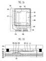
- FIG. 7Dschematically illustrates a cross-section of an encapsulated OLED device 1011 having a layout of FIG. 7C and taken along the line d-d of FIG. 7C .
- a generally planar top plate or substrate 1061engages with a seal 1071 which further engages with a bottom plate or substrate 1002 to enclose or encapsulate the OLED pixel array 1021 .
- one or more layersare formed on the top plate 1061 or bottom plate 1002 , and the seal 1071 is coupled with the bottom or top substrate 1002 , 1061 via such a layer.
- the seal 1071extends along the periphery of the OLED pixel array 1021 or the bottom or top plate 1002 , 1061 .
- the seal 1071is made of a frit material as will be further discussed below.
- the top and bottom plates 1061 , 1002comprise materials such as plastics, glass and/or metal foils which can provide a barrier to passage of oxygen and/or water to thereby protect the OLED pixel array 1021 from exposure to these substances.
- at least one of the top plate 1061 and the bottom plate 1002are formed of a substantially transparent material.
- seal 1071 and the top and bottom plates 1061 , 1002provide a substantially non-permeable seal to oxygen and water vapor and provide a substantially hermetically enclosed space 1081 .
- the seal 1071 of a frit material in combination with the top and bottom plates 1061 , 1002provide a barrier to oxygen of less than approximately 10 ⁇ 3 cc/m 2 -day and to water of less than 10 ⁇ 6 g/m 2 -day.
- a material that can take up oxygen and/or moistureis formed within the enclosed space 1081 .
- the seal 1071has a width W, which is its thickness in a direction parallel to a surface of the top or bottom substrate 1061 , 1002 as shown in FIG. 7D .
- the widthvaries among embodiments and ranges from about 300 ⁇ m to about 3000 ⁇ m, optionally from about 500 ⁇ m to about 1500 ⁇ m. Also, the width may vary at different positions of the seal 1071 . In some embodiments, the width of the seal 1071 may be the largest where the seal 1071 contacts one of the bottom and top substrate 1002 , 1061 or a layer formed thereon. The width may be the smallest where the seal 1071 contacts the other.
- the width variation in a single cross-section of the seal 1071relates to the cross-sectional shape of the seal 1071 and other design parameters.
- the seal 1071has a height H, which is its thickness in a direction perpendicular to a surface of the top or bottom substrate 1061 , 1002 as shown in FIG. 7D .
- the heightvaries among embodiments and ranges from about 2 ⁇ m to about 30 ⁇ m, optionally from about 10 ⁇ m to about 15 ⁇ m. Generally, the height does not significantly vary at different positions of the seal 1071 . However, in certain embodiments, the height of the seal 1071 may vary at different positions thereof.
- the seal 1071has a generally rectangular cross-section. In other embodiments, however, the seal 1071 can have other various cross-sectional shapes such as a generally square cross-section, a generally square cross-section, a generally trapezoidal cross-section, a cross-section with one or more rounded edges, or other configuration as indicated by the needs of a given application. To improve hermetically, it is generally desired to increase the interfacial area where the seal 1071 directly contacts the bottom or top substrate 1002 , 1061 or a layer formed thereon. In some embodiments, the shape of the seal can be designed such that the interfacial area can be increased.
- the seal 1071can be arranged immediately adjacent the OLED array 1021 , and in other embodiments, the seal 1071 is spaced some distance from the OLED array 1021 .
- the seal 1071comprises generally linear segments that are connected together to surround the OLED array 1021 . Such linear segments of the seal 1071 can extend, in certain embodiments, generally parallel to respective boundaries of the OLED array 1021 .
- one or more of the linear segments of the seal 1071are arranged in a non-parallel relationship with respective boundaries of the OLED array 1021 .
- at least part of the seal 1071extends between the top plate 1061 and bottom plate 1002 in a curvilinear manner.
- the seal 1071is formed using a frit material or simply “frit” or glass frit,” which includes fine glass particles.
- the frit particlesincludes one or more of magnesium oxide (MgQ), calcium oxide (CaO), barium oxide (BaO), lithium oxide (Li 2 O), sodium oxide (Na 2 O), potassium oxide (K 2 O), boron oxide (B 2 O 3 ), vanadium oxide (V 2 O 5 ), zinc oxide (ZnO), tellurium oxide (TeO 2 ), aluminum oxide (Al 2 O 3 ), silicon dioxide (SiO 2 ), lead oxide (PbO), tin oxide (SnO), phosphorous oxide (P 2 O 5 ), ruthenium oxide (Ru 2 O), rubidium oxide (Rb 2 O), rhodium oxide (Rh 2 O), ferrite oxide (Fe 2 O 3 ), copper oxide (CuO), titanium oxide (TiO 2 ), tungsten oxide (WO 3 ), bismuth oxide (Bi 2
- these particlesrange in size from about 2 ⁇ m to about 30 ⁇ m, optionally about 5 ⁇ m to about 10 ⁇ m, although not limited only thereto.
- the particlescan be as large as about the distance between the top and bottom substrates 1061 , 1002 or any layers formed on these substrates where the frit seal 1071 contacts.
- the frit material used to form the seal 1071can also include one or more filler or additive materials.
- the filler or additive materialscan be provided to adjust an overall thermal expansion characteristic of the seal 1071 and/or to adjust the absorption characteristics of the seal 1071 for selected frequencies of incident radiant energy.
- the filler or additive material(s)can also include inversion and/or additive fillers to adjust a coefficient of thermal expansion of the frit.
- the filler or additive materialscan include transition metals, such as chromium (Cr), iron (Fe), manganese (Mn), cobalt (Co), copper (Cu), and/or vanadium. Additional materials for the filler or additives include ZnSiO 4 , PbTiO 3 , ZrO 2 , eucryptite.
- a frit material as a dry compositioncontains glass particles from about 20 to 90 about wt %, and the remaining includes fillers and/or additives.
- the frit pastecontains about 10-30 wt % organic materials and about 70-90% inorganic materials.
- the frit pastecontains about 20 wt % organic materials and about 80 wt % inorganic materials.
- the organic materialsmay include about 0-30 wt % binder(s) and about 70-100 wt % solvent(s).
- about 10 wt %is binder(s) and about 90 wt % is solvent(s) among the organic materials.
- the inorganic materialsmay include about 0-10 wt % additives, about 20-40 wt % fillers and about 50-80 wt % glass powder. In some embodiments, about 0-5 wt % is additive(s), about 25-30 wt % is filler(s) and about 65-75 wt % is the glass powder among the inorganic materials.
- a liquid materialis added to the dry frit material to form a frit paste.
- Any organic or inorganic solvent with or without additivescan be used as the liquid material.
- the solventincludes one or more organic compounds.
- applicable organic compoundsare ethyl cellulose, nitro cellulose, hydroxyl propyl cellulose, butyl carbitol acetate, terpineol, butyl cellusolve, acrylate compounds.
- a shape of the seal 1071is initially formed from the frit paste and interposed between the top plate 1061 and the bottom plate 1002 .
- the seal 1071can in certain embodiments be pre-cured or pre-sintered to one of the top plate and bottom plate 1061 , 1002 .
- portions of the seal 1071are selectively heated such that the frit material forming the seal 1071 at least partially melts.
- the seal 1071is then allowed to resolidify to form a secure joint between the top plate 1061 and the bottom plate 1002 to thereby inhibit exposure of the enclosed OLED pixel array 1021 to oxygen or water.
- the selective heating of the frit sealis carried out by irradiation of light, such as a laser or directed infrared lamp.
- the frit material forming the seal 1071can be combined with one or more additives or filler such as species selected for improved absorption of the irradiated light to facilitate heating and melting of the frit material to form the seal 1071 .
- OLED devices 1011are mass produced.
- a plurality of separate OLED arrays 1021is formed on a common bottom substrate 1101 .
- each OLED array 1021is surrounded by a shaped frit to form the seal 1071 .
- common top substrate(not shown) is placed over the common bottom substrate 1101 and the structures formed thereon such that the OLED arrays 1021 and the shaped frit paste are interposed between the common bottom substrate 1101 and the common top substrate.
- the OLED arrays 1021are, encapsulated and sealed, such as via the previously described enclosure process for a single OLED display device.
- the resulting productincludes a plurality of OLED devices kept together by the common bottom and top substrates. Then, the resulting product is cut into a plurality of pieces, each of which constitutes an OLED device 1011 of FIG. 7D . In certain embodiments, the individual OLED devices 1011 then further undergo additional packaging operations to further improve the sealing formed by the frit seal 1071 and the top and bottom substrates 1061 , 1002 .
- FIGS. 1A , 2 A and 3 Aare plan views for illustrating a manufacturing method of an organic light emitting display device (OLED) according to a first embodiment, and FIGS. 1B , 2 B and 3 B are cross-sectional views thereof.
- OLEDorganic light emitting display device
- a substrate 200includes a pixel region 210 and a non-pixel region 220 surrounding the pixel region 210 .
- the pixel region 210 of the substrate 200may include multiple organic light emitting elements 100 , which are connected to one another in the matrix form between a scan line 104 b and a data line 106 c .
- the non-pixel region 220 of the substrate 200may include i) a scan line 104 b and a data line 106 c extending from the scan line 104 b and the data line 106 c , respectively, of the pixel region 210 , ii) a power supply line (not shown) for generating the organic light emitting elements 100 , and iii) a scan driver 410 and a data driver 420 for processing signals from the external through pads 104 c and 106 d and supplying them to the scan line 104 b and data line 106 c.
- the organic light emitting element 100may include an anode electrode 108 and cathode electrode 111 , and an organic thin film layer 110 formed between the anode electrode 108 and cathode electrode 111 .
- the organic thin film layer 110may include a hole transport layer, an organic light-emitting layer and an electron transport layer, and may further include an hole injection layer and an electron injection layer.
- the organic light emitting elements 100may further include a switching transistor for controlling their operation and a capacitor for maintaining signals.
- a buffer layer 101may be formed on the pixel region 210 and non-pixel region 220 of the substrate 200 .
- the buffer layer 101serves to prevent damages to the substrate 200 due to heat and to isolate diffusion of ions from the substrate 200 to the outside.
- the buffer layer 101may be formed as an insulating film such as silicon oxide film SiO 2 or silicon nitride film SiNx.
- a semiconductor layer 102which serves as an active layer, may be formed over the buffer layer 101 of the pixel region 210 . Then, a gate insulating film 103 is formed over the substantially entire upper surface of the pixel region 210 including the semi conductor layer 102 .
- a gate electrode 104 amay be formed over the gate insulating film 103 which is over the upper side of the semiconductor layer 102 .
- the pixel region 210may include a scan line connected to the gate electrode 104 a .
- the non-pixel region 220may include a scan line 104 b extending from the scan line 104 of the pixel region 210 and a pad 104 c to receive signals from external sources.
- the gate electrode 104 a , scan line 104 b and pad 104 cmay include metals such as Mo, W, Ti, Al, or an alloy thereof, and may have a stacked layer structure.
- An interlayer insulating film 105may be formed over the substantially entire upper surface of the pixel region 210 including the gate electrode 104 a .
- Contact holesmay be formed to expose predetermined portions of the semiconductor layer 102 through the between-layer insulating film 105 and gate insulating film 103 .
- a source electrode 106 a and a drain electrode 106 bare formed to be connected through the contact holes to the semiconductor layer 102 .
- the pixel region 210may include a data line 106 c connected to the source and drain electrodes 106 a , 106 b and the non-pixel region 220 may include a data line 106 c extending from the data line 106 c of the pixel region 210 and a pad 106 d to receive signals from the external sources.
- the source and drain electrodes 106 a and 106 b , data line 106 c and pad 106 dmay include a metal such as Mo, W, Ti, Al, or an alloy thereof, and may be formed as a
- a planarization layer 107may be formed over the substantially entire upper surface of the pixel region 210 to planarize the upper surface of the partially fabricated device described above.
- a via holemay be formed to expose predetermined parts of the source or drain electrode 106 a or 106 b .
- An anode electrode 108may be formed to be connected through the via hole to the source or drain electrode 106 a or 106 b.
- a pixel definition film 109is formed over the planarization layer 107 so that a part of the anode electrode 108 is exposed. Then, an organic thin film 110 is formed on the exposed anode electrode 108 . A cathode electrode 111 is formed on the pixel definition film 109 including the organic thin film layer 110 .
- an encapsulation substrate 300is provided.
- the encapsulation substrate 300has a size sufficient to cover the pixel region 210 and at least a portion of the non-pixel region 220 .
- the encapsulation substrate 300may include a transparent material such as glass.
- the encapsulation substratemay include silicon oxide SiO 2 .
- a frit 320may be formed on peripheral regions of the encapsulation substrate 300 which correspond to the non-pixel region 220 of the substrate 200 .
- the frit 320serves to seal the pixel region 210 to prevent a gas such as hydrogen and oxygen or moisture from being penetrated.
- the frit 320is formed to surround a part of the non-pixel region 220 and the pixel region 210 .
- a complementary moisture absorbentmay further be added to the region enclosed by the frit 320 .
- fluorescencemay refer to a powder-type glass material.
- “frit”may also refer to a frit in a paste form, which may include a laser absorber, an organic binder, a filler for reducing the thermal expansion coefficient, etc.
- “frit”may refer to a seal formed by curing the frit paste by a laser beam or infrared ray.
- a glass frit in a paste formmay include at least one kind of transition metal.
- the fritmay be applied to the encapsulation substrate with a height of about 14 to about 50 ⁇ m and a width of about 0.6 to about 1.5 mm using a screen printing or dispensing method. After that, the frit may be sintered so as to eliminate its moisture or organic binder, and then is cured.
- the encapsulation substrate 300is arranged over the upper surface of the substrate 200 , on which the organic light emitting element 100 is formed, as shown in FIGS. 1A and 1B .
- the encapsulation substrate 300covers the pixel region 210 and at least a portion of the non-pixel region 220 .
- the frit 320may be fused to be attached to the substrate 200 by illuminating a laser beam onto the frit 320 from above the encapsulation substrate 300 .
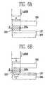
- FIGS. 4A and 4Bare views of illustrating one embodiment of curing the frit 320 between the substrate 200 and the encapsulation substrate 300 .
- the laser beamis adjusted to have a width A or diameter larger than a width B of the frit.
- a laser beamhas a width A in the cross-sectional illustration, which is perpendicular to the direction in which the laser beam travels and the frit is elongated.
- the width of a fritrefers to the length of the cross-section of a frit in the direction where the width A of the laser beam is measured, as shown in FIG. 6A .
- the OLEDincludes a fit 320 having portions surrounding the pixel region 210 .
- one of the fit portionsextends in a direction D.
- the cross-section 320 ais taken substantially perpendicular to the direction D.
- the width of the cross-section 320 arefers to a width B extending substantially parallel to at least one of the substrates 200 , 300 .
- the width B of the fit 320is the same throughout the entire cross-section 320 a of the fit, as shown in FIG. 6A .
- the fritmay have several different widths. For example, in FIG.
- the frit 320has a tapered portion penetrating through the planarization layer 107 down to the substrate 200 .
- the tapered portionnarrows as it extends toward the substrate 200 .
- the width of the fritrefers to the longest width B, e.g., throughout the cross section 320 b of the frit as shown in FIG. 6B , rather than other widths such as a width C which is the shortest.
- the laser beamis irradiated from above the encapsulation substrate.
- the illustrated laser beamhas a width A.
- the fritmay have a width B which is smaller than the width A of the laser beam.
- the laser beammay be adjusted to have a width which is about 0.6 to about 1.5 mm larger than the width of the frit.
- the lasermay be adjusted to have a power of about 36 to about 38 W.
- the lasermay be moved at a constant speed, for example, about 10 to about 40 mm/sec, optionally 20 mm/sec, along the frit 320 to maintain a constant fusion temperature and adhesive strength.
- the laser beam widthmay be substantially equal to or smaller than the frit width. In such embodiments, the laser beam may be moved to over edge portions of the frit to effect curing of the edge portions.
- regions off from the center of the laser beam by a predetermined distanceare also illuminated uniformly by the laser beam since the width A of the laser beam is adapted to be larger than the width B of the frit, and thus curing may be completed well all over the frit.
- the display devicemay be designed such that the laser beam is not illuminated onto a pattern such as a metal line in the non-pixel region 220 of the substrate 200 .
- a patternmay be positioned in a region not exposed to the laser beam.
- the patternmay be within a region exposed to the laser beam as long as the pattern can be blocked by a certain structure in the region from the laser beam.
- the frit 320is formed to seal only the pixel region 210 .
- the fritmay enclose the scan driver 410 as well.
- the size of the encapsulation substrate 300may need to be changed.
- the frit 320may be first formed on the substrate 200 , and then the encapsulation substrate 300 may be placed over the substrate 200 .
- a laserhas been employed to fuse and attach the frit 320 to the substrate 200
- other light sourcessuch as an infrared light may also be used.
- FIGS. 5A and 5Bare views of illustrating a second embodiment where a width of a laser beam is adjusted so that solid lines are formed in a predetermined ratio of a width of a frit. Detailed description of the second embodiment will be omitted since the first embodiment may be referred to herein.
- the first substrate 500 and the second substrate 600are attached to each other by illuminating a laser beam with a width A′ larger than a width B′ of the frit from above the second substrate 600 .
- the laser beammay be adjusted to have a width which is about 0.6 to about 1.5 mm larger than the width B of the frit.
- the lasermay be adjusted to have a power of about 36 to about 38 W.
- the lasermay be moved at a constant speed, for example, about 10 to about 40 mm/sec, optionally 20 mm/sec, along the frit 520 to maintain a constant fusion temperature and adhesive strength.
- the width, in which the frit 520 is substantially cured by the mid-portion of the laser beam,is determined. That is, the mid-portion of the frit 520 is cured such that a solid line 521 is formed on the mid-portion of the frit 520 .
- the width C′ of the solid line 521 of the frit 520is about 50 to about 80% of the width of the frit.
- the width of the laser beammay be adjusted in power so that the width C′ of the solid line 521 has a predetermined percentage of the width B′ of the frit.
- regions off from the mid-portion of the laser beam by a predetermined distanceare also illuminated uniformly by the laser beam since the width A′ of the laser beam is adapted to be larger than the width B′ of the frit, and the solid line 521 is formed by a predetermined percentage of the frit 520 , so that curing may be done well all over the frit.
Landscapes
- Physics & Mathematics (AREA)
- Optics & Photonics (AREA)
- Electroluminescent Light Sources (AREA)
- Devices For Indicating Variable Information By Combining Individual Elements (AREA)
Abstract
Description
| Application | ||
| Title | Filing Date | No. |
| ORGANIC LIGHT-EMITTING DISPLAY | Sep. 29, 2006 | 11/541,055 |
| DEVICE AND METHOD OF | ||
| FABRICATING THE SAME | ||
| ORGANIC LIGHT-EMITTING DISPLAY | Sep. 29, 2006 | 11/529,914 |
| DEVICE AND METHOD OF | ||
| MANUFACTURING THE SAME | ||
| ORGANIC LIGHT EMITTING DISPLAY | Sep. 29, 2006 | 11/541,139 |
| DEVICE | ||
| ORGANIC LIGHT-EMITTING DISPLAY | Sep. 29, 2006 | 11/541,047 |
| DEVICE WITH FRIT SEAL AND | ||
| REINFORCING STRUCTURE | ||
| ORGANIC LIGHT EMITTING DISPLAY | Sep. 29, 2006 | 11/540,150 |
| DEVICE METHOD OF FABRICATING | ||
| THE SAME | ||
| ORGANIC LIGHT EMITTING DISPLAY | Sep. 29, 2006 | 11/541,009 |
| AND METHOD OF FABRICATING THE | ||
| SAME | ||
| ORGANIC LIGHT-EMITTING DISPLAY | Sep. 29, 2006 | 11/540,151 |
| DEVICE WITH FRIT SEAL AND | ||
| REINFORCING STRUCTURE BONDED | ||
| TO FRAME | ||
| METHOD FOR PACKAGING ORGANIC | Sep. 29, 2006 | 11/529,910 |
| LIGHT EMITTING DISPLAY WITH | ||
| FRIT SEAL AND REINFORCING | ||
| STURUTURE | ||
| METHOD FOR PACKAGING ORGANIC | Sep. 29, 2006 | 11/540,084 |
| LIGHT EMITTING DISPLAY WITH | ||
| FRIT SEAL AND REINFORCING | ||
| STURUTURE | ||
| ORGANIC LIGHT-EMITTING DISPLAY | Sep. 29, 2006 | 11/540,008 |
| DEVICE AND THE PREPARATION | ||
| METHOD OF THE SAME | ||
| ORGANIC LIGHT EMITTING DISPLAY | Sep. 29, 2006 | 11/541,048 |
| AND FABRICATING METHOD OF THE | ||
| SAME | ||
| ORGANIC LIGHT-EMITTING DISPLAY | Sep. 29, 2006 | 11/540,021 |
| AND METHOD OF MAKING THE | ||
| SAME | ||
| ORGANIC LIGHT EMITTING DISPLAY | Sep. 29, 2006 | 11/540,024 |
| AND FABRICATING METHOD OF THE | ||
| SAME | ||
| ORGANIC LIGHT-EMITTING DISPLAY | Sep. 29, 2006 | 11/540,157 |
| DEVICE AND MANUFACTURING | ||
| METHOD OF THE SAME | ||
| ORGANIC LIGHT EMITTING DISPLAY | Sep. 29, 2006 | 11/540,149 |
| AND FABRICATING METHOD OF THE | ||
| SAME | ||
| ORGANIC LIGHT EMITTING DISPLAY | Sep. 29, 2006 | 11/529,916 |
| AND METHOD OF FABRICATING THE | ||
| SAME | ||
| ORGANIC LIGHT EMITTING DISPLAY | Sep. 29, 2006 | 11/529,891 |
| DEVICE METHOD OF FABRICATING | ||
| THE SAME | ||
| ORGANIC LIGHT EMITTING DISPLAY | Sep. 29, 2006 | 11/540,103 |
| AND METHOD OF FABRICATING THE | ||
| SAME | ||
Claims (13)
Applications Claiming Priority (4)
| Application Number | Priority Date | Filing Date | Title |
|---|---|---|---|
| KR1020060008462AKR100671642B1 (en) | 2006-01-26 | 2006-01-26 | Manufacturing method of organic light emitting display device |
| KR10-2006-0008462 | 2006-01-26 | ||
| KR10-2006-0016188 | 2006-02-20 | ||
| KR1020060016188AKR100754120B1 (en) | 2006-02-20 | 2006-02-20 | Manufacturing method of organic light emitting display device |
Publications (2)
| Publication Number | Publication Date |
|---|---|
| US20070171637A1 US20070171637A1 (en) | 2007-07-26 |
| US8299705B2true US8299705B2 (en) | 2012-10-30 |
Family
ID=37913664
Family Applications (1)
| Application Number | Title | Priority Date | Filing Date |
|---|---|---|---|
| US11/529,995Active2029-03-27US8299705B2 (en) | 2006-01-26 | 2006-09-29 | Organic light emitting display device and manufacturing method thereof |
Country Status (4)
| Country | Link |
|---|---|
| US (1) | US8299705B2 (en) |
| EP (1) | EP1814187A3 (en) |
| JP (1) | JP4633674B2 (en) |
| TW (1) | TWI461094B (en) |
Cited By (15)
| Publication number | Priority date | Publication date | Assignee | Title |
|---|---|---|---|---|
| US20120075823A1 (en)* | 2010-09-28 | 2012-03-29 | Samsung Electronics Co. Ltd. | Display panel and method of manufacturing the same |
| US20120104933A1 (en)* | 2010-10-27 | 2012-05-03 | Samsung Mobile Display Co., Ltd. | Organic Light Emitting Display Apparatus and Method of Manufacturing the Same |
| US20120168808A1 (en)* | 2010-12-30 | 2012-07-05 | Chunghwa Picture Tubes, Ltd. | Package structure |
| US20140132149A1 (en)* | 2012-11-13 | 2014-05-15 | Samsung Display Co., Ltd. | Organic light emitting display apparatus and method of manufacturing the same |
| US9004972B2 (en) | 2006-01-20 | 2015-04-14 | Samsung Display Co., Ltd. | Organic light-emitting display device with frit seal and reinforcing structure |
| US20150243923A1 (en)* | 2012-09-28 | 2015-08-27 | Osram Oled Gmbh | Optoelectronic component and method for producing an optoelectronic component |
| US20150263310A1 (en)* | 2014-03-17 | 2015-09-17 | Samsung Display Co., Ltd. | Organic light emitting display and manufacturing method for the same |
| US20150349288A1 (en)* | 2014-05-29 | 2015-12-03 | Boe Technology Group Co., Ltd. | Light emitting display panel and manufacturing method thereof |
| US20170098797A1 (en)* | 2015-10-06 | 2017-04-06 | Samsung Display Co., Ltd. | Display apparatus |
| US10319800B2 (en)* | 2016-06-20 | 2019-06-11 | Wuhan China Star Optoelectronics Technology Co., Ltd | OLED display screen |
| US10396136B2 (en) | 2015-02-24 | 2019-08-27 | Samsung Display Co., Ltd. | Organic light-emitting display device |
| US10497898B2 (en) | 2015-11-24 | 2019-12-03 | Corning Incorporated | Sealed device housing with particle film-initiated low thickness laser weld and related methods |
| US20210296609A1 (en)* | 2020-03-17 | 2021-09-23 | Samsung Display Co., Ltd. | Display device |
| US20210408433A1 (en)* | 2020-06-25 | 2021-12-30 | Samsung Display Co., Ltd. | Display device and method of fabricating the same |
| US12317733B2 (en) | 2019-03-13 | 2025-05-27 | Samsung Display Co., Ltd. | Display apparatus and method of manufacturing the same |
Families Citing this family (48)
| Publication number | Priority date | Publication date | Assignee | Title |
|---|---|---|---|---|
| US20070108900A1 (en)* | 2005-11-15 | 2007-05-17 | Boek Heather D | Method and apparatus for the elimination of interference fringes in an OLED device |
| US7597603B2 (en)* | 2005-12-06 | 2009-10-06 | Corning Incorporated | Method of encapsulating a display element |
| US7537504B2 (en)* | 2005-12-06 | 2009-05-26 | Corning Incorporated | Method of encapsulating a display element with frit wall and laser beam |
| US7425166B2 (en)* | 2005-12-06 | 2008-09-16 | Corning Incorporated | Method of sealing glass substrates |
| US8038495B2 (en) | 2006-01-20 | 2011-10-18 | Samsung Mobile Display Co., Ltd. | Organic light-emitting display device and manufacturing method of the same |
| KR100635514B1 (en) | 2006-01-23 | 2006-10-18 | 삼성에스디아이 주식회사 | Organic light emitting display device and manufacturing method |
| JP4456092B2 (en)* | 2006-01-24 | 2010-04-28 | 三星モバイルディスプレイ株式會社 | Organic electroluminescent display device and manufacturing method thereof |
| JP4624309B2 (en)* | 2006-01-24 | 2011-02-02 | 三星モバイルディスプレイ株式會社 | Organic electroluminescent display device and manufacturing method thereof |
| KR100671641B1 (en) | 2006-01-25 | 2007-01-19 | 삼성에스디아이 주식회사 | Organic electroluminescent display and manufacturing method thereof |
| KR100688796B1 (en)* | 2006-01-25 | 2007-03-02 | 삼성에스디아이 주식회사 | Organic light emitting display device and manufacturing method thereof |
| KR100685853B1 (en)* | 2006-01-25 | 2007-02-22 | 삼성에스디아이 주식회사 | Organic light emitting display device and manufacturing method |
| KR100688795B1 (en)* | 2006-01-25 | 2007-03-02 | 삼성에스디아이 주식회사 | Organic light emitting display device and manufacturing method |
| US8164257B2 (en)* | 2006-01-25 | 2012-04-24 | Samsung Mobile Display Co., Ltd. | Organic light emitting display and method of fabricating the same |
| KR100671647B1 (en)* | 2006-01-26 | 2007-01-19 | 삼성에스디아이 주식회사 | Organic light emitting display device |
| KR100732808B1 (en)* | 2006-01-26 | 2007-06-27 | 삼성에스디아이 주식회사 | Manufacturing method of organic light emitting display device |
| KR100671639B1 (en)* | 2006-01-27 | 2007-01-19 | 삼성에스디아이 주식회사 | Organic electroluminescent display and manufacturing method thereof |
| KR100688790B1 (en)* | 2006-01-27 | 2007-03-02 | 삼성에스디아이 주식회사 | Organic electroluminescent display and manufacturing method thereof |
| US20070188757A1 (en)* | 2006-02-14 | 2007-08-16 | Jeffrey Michael Amsden | Method of sealing a glass envelope |
| KR100732817B1 (en) | 2006-03-29 | 2007-06-27 | 삼성에스디아이 주식회사 | Organic light emitting display device and manufacturing method |
| US20070267972A1 (en)* | 2006-05-22 | 2007-11-22 | Menegus Harry E | Method for forming a temporary hermetic seal for an OLED display device |
| US20080124558A1 (en)* | 2006-08-18 | 2008-05-29 | Heather Debra Boek | Boro-silicate glass frits for hermetic sealing of light emitting device displays |
| US20080049431A1 (en)* | 2006-08-24 | 2008-02-28 | Heather Debra Boek | Light emitting device including anti-reflection layer(s) |
| US20080048556A1 (en)* | 2006-08-24 | 2008-02-28 | Stephan Lvovich Logunov | Method for hermetically sealing an OLED display |
| US7800303B2 (en) | 2006-11-07 | 2010-09-21 | Corning Incorporated | Seal for light emitting display device, method, and apparatus |
| US20080168801A1 (en)* | 2007-01-12 | 2008-07-17 | Paul Stephen Danielson | Method of sealing glass |
| US20080200088A1 (en)* | 2007-02-21 | 2008-08-21 | Chong Pyung An | Method for reducing interference fringes in a display device |
| US7652305B2 (en)* | 2007-02-23 | 2010-01-26 | Corning Incorporated | Methods and apparatus to improve frit-sealed glass package |
| US20080213482A1 (en)* | 2007-03-01 | 2008-09-04 | Stephan Lvovich Logunov | Method of making a mask for sealing a glass package |
| US8716850B2 (en)* | 2007-05-18 | 2014-05-06 | Semiconductor Energy Laboratory Co., Ltd. | Semiconductor device and method for manufacturing the same |
| JP2009199858A (en)* | 2008-02-21 | 2009-09-03 | Seiko Epson Corp | Method of manufacturing light-emitting device |
| US20090295277A1 (en)* | 2008-05-28 | 2009-12-03 | Stephan Lvovich Logunov | Glass packages and methods of controlling laser beam characteristics for sealing them |
| US8448468B2 (en) | 2008-06-11 | 2013-05-28 | Corning Incorporated | Mask and method for sealing a glass envelope |
| US20100095705A1 (en) | 2008-10-20 | 2010-04-22 | Burkhalter Robert S | Method for forming a dry glass-based frit |
| DE102009035392A1 (en)* | 2009-07-30 | 2011-02-03 | Osram Opto Semiconductors Gmbh | Organic component and process for its production |
| JP2011060697A (en)* | 2009-09-14 | 2011-03-24 | Canon Inc | Manufacturing method of image display device |
| KR101135538B1 (en)* | 2009-11-16 | 2012-04-13 | 삼성모바일디스플레이주식회사 | Display device and method for menufacturing display device |
| KR101074812B1 (en)* | 2010-01-05 | 2011-10-19 | 삼성모바일디스플레이주식회사 | Organic light-emitting display device and manufacturing method of the same |
| JP5659511B2 (en) | 2010-03-11 | 2015-01-28 | 住友化学株式会社 | Electrical equipment |
| KR101754916B1 (en)* | 2010-11-08 | 2017-07-20 | 삼성디스플레이 주식회사 | Organic light emitting diode display and manufacturing method of the same |
| WO2013031509A1 (en)* | 2011-08-26 | 2013-03-07 | Semiconductor Energy Laboratory Co., Ltd. | Light-emitting device, electronic device, lighting device, and method for manufacturing the light-emitting device |
| WO2013171966A1 (en)* | 2012-05-14 | 2013-11-21 | シャープ株式会社 | Organic el display apparatus |
| WO2014035954A2 (en) | 2012-08-30 | 2014-03-06 | Corning Incorporated | Antimony-free glass, antimony-free frit and a glass package that is hermetically sealed with the frit |
| US8883527B2 (en)* | 2012-09-06 | 2014-11-11 | Shenzhen China Star Optoelectronics Technology Co., Ltd. | Organic light-emitting diode display panel and manufacturing method for the same |
| KR102048927B1 (en)* | 2013-02-07 | 2019-11-27 | 삼성디스플레이 주식회사 | Organic luminescence emitting display device and method for preparing the same |
| CN103440824B (en)* | 2013-08-07 | 2016-08-10 | 北京京东方光电科技有限公司 | A kind of organic EL display panel, its manufacture method and display device |
| KR102295536B1 (en) | 2014-07-25 | 2021-08-31 | 삼성디스플레이 주식회사 | Display module, display device and method for manufacturing the same |
| KR102360092B1 (en) | 2015-01-22 | 2022-02-09 | 삼성디스플레이 주식회사 | Organic light emitting display apparatus and manufacturing method of the same |
| KR102349282B1 (en)* | 2015-03-27 | 2022-01-11 | 삼성디스플레이 주식회사 | Display apparatus and method for manufacturing the same |
Citations (153)
| Publication number | Priority date | Publication date | Assignee | Title |
|---|---|---|---|---|
| US3966449A (en) | 1975-02-10 | 1976-06-29 | International Business Machines Corporation | Sealing glass composition and process |
| US4004936A (en)* | 1976-05-19 | 1977-01-25 | International Business Machines Corporation | Low temperature sealed glass compositions and process for their preparation |
| US4105292A (en) | 1975-09-02 | 1978-08-08 | Minnesota Mining And Manufacturing Company | Optical element to assure a minimum spacing |
| US4238704A (en) | 1979-02-12 | 1980-12-09 | Corning Glass Works | Sealed beam lamp of borosilicate glass with a sealing glass of zinc silicoborate and a mill addition of cordierite |
| US4702566A (en) | 1984-04-12 | 1987-10-27 | Asahi Glass Company Ltd. | Electrochromic display device |
| US4826297A (en) | 1985-12-25 | 1989-05-02 | Hitachi, Ltd. | Liquid crystal display device having an extention metal film wiring which is covered by polyimide layer having low viscosity under 1.0 poise before curing |
| US4984059A (en) | 1982-10-08 | 1991-01-08 | Fujitsu Limited | Semiconductor device and a method for fabricating the same |
| US5808719A (en) | 1994-09-02 | 1998-09-15 | Sharp Kabushiki Kaisha | Liquid crystal display apparatus wherein plurality display panels makes display surfaces flush by perming junction panel and producing method thereof |
| US5811927A (en) | 1996-06-21 | 1998-09-22 | Motorola, Inc. | Method for affixing spacers within a flat panel display |
| US5965907A (en) | 1997-09-29 | 1999-10-12 | Motorola, Inc. | Full color organic light emitting backlight device for liquid crystal display applications |
| US6005653A (en) | 1997-10-09 | 1999-12-21 | Nec Corporation | Method and apparatus for sealing liquid crystal display element cell |
| US6087717A (en) | 1997-03-24 | 2000-07-11 | Texas Instruments Incorporated | Semiconductor device and manufacturing method |
| US6109994A (en) | 1996-12-12 | 2000-08-29 | Candescent Technologies Corporation | Gap jumping to seal structure, typically using combination of vacuum and non-vacuum environments |
| JP2001022293A (en) | 1999-07-07 | 2001-01-26 | Sony Corp | Planar display element |
| JP2001052858A (en) | 1999-08-05 | 2001-02-23 | Futaba Corp | Organic el display device |
| US6195142B1 (en) | 1995-12-28 | 2001-02-27 | Matsushita Electrical Industrial Company, Ltd. | Organic electroluminescence element, its manufacturing method, and display device using organic electroluminescence element |
| US6210815B1 (en) | 1997-12-17 | 2001-04-03 | Nec Corporation | Organic thin film EL device and method for making the same |
| US6211938B1 (en) | 1997-09-18 | 2001-04-03 | Nec Corporation | Apparatus for manufacturing a plurality of liquid crystal panels using press and pressurized regions |
| CN1290121A (en) | 1999-09-27 | 2001-04-04 | 索尼株式会社 | Printed circuit board and display device |
| JP2001110564A (en) | 1999-10-07 | 2001-04-20 | Gunze Ltd | Electroluminescence lamp |
| JP2001203076A (en) | 1999-11-09 | 2001-07-27 | Semiconductor Energy Lab Co Ltd | Light emitting device and manufacturing method thereof |
| JP2001230072A (en) | 2000-02-18 | 2001-08-24 | Denso Corp | Organic el display device |
| US6288487B1 (en) | 1999-03-17 | 2001-09-11 | Tdk Corporation | Organic electroluminescent device with a high-resistance inorganic electron injecting and transporting layer |
| JP2001319775A (en) | 2000-05-10 | 2001-11-16 | Auto Network Gijutsu Kenkyusho:Kk | Sealing method and sealing structure for organic EL display device |
| JP2001324662A (en) | 2000-05-16 | 2001-11-22 | Ricoh Co Ltd | Lens interlocking mechanism |
| JP2002020169A (en) | 2000-07-03 | 2002-01-23 | Murata Mfg Co Ltd | High-frequecy dielectric porcelain composition, dielectric resonator, dielectric filter, dielectric duplexer and communications equipment |
| JP2002100472A (en) | 2000-07-10 | 2002-04-05 | Semiconductor Energy Lab Co Ltd | Film-forming apparatus, light-emitting device and its method of manufacturing the device |
| JP2002117777A (en) | 2000-10-11 | 2002-04-19 | Matsushita Electric Ind Co Ltd | Gas discharge panel and its manufacturing method |
| JP2002170664A (en) | 2000-12-05 | 2002-06-14 | Toray Ind Inc | Organic electroluminescent device |
| US6424009B1 (en) | 2001-05-04 | 2002-07-23 | Advanced Micro Devices, Inc. | Polysilicon insulator material in semiconductor-on-insulator (SOI) structure |
| JP2002216951A (en) | 2000-11-14 | 2002-08-02 | Semiconductor Energy Lab Co Ltd | Light emitting device |
| US6452323B1 (en) | 1999-09-20 | 2002-09-17 | Omnion Technologies, Inc. | Luminous gas discharge display having dielectric sealing layer |
| JP2002280169A (en) | 2001-03-19 | 2002-09-27 | Futaba Corp | Organic EL device |
| JP2002318547A (en) | 2001-04-24 | 2002-10-31 | Sony Corp | Method of manufacturing display panel |
| US6489719B1 (en) | 1999-06-03 | 2002-12-03 | Koninklijke Philips Electronics N.V. | Organic electroluminescent device |
| JP2002359070A (en) | 2001-05-31 | 2002-12-13 | Matsushita Electric Ind Co Ltd | Organic light emitting device and display panel using the same |
| US6495262B2 (en) | 2000-04-20 | 2002-12-17 | Mitsubishi Denki Kabushiki Kaisha | Flat display panel, flat display device and flat display panel manufacturing method |
| US6515417B1 (en) | 2000-01-27 | 2003-02-04 | General Electric Company | Organic light emitting device and method for mounting |
| US20030066311A1 (en) | 2001-10-09 | 2003-04-10 | Chien-Hsing Li | Encapsulation of a display element and method of forming the same |
| US6551724B2 (en) | 1999-12-28 | 2003-04-22 | Nec Corporation | Organic electro-luminescent display panel |
| US20030077396A1 (en) | 2001-10-23 | 2003-04-24 | Lecompte Robert S. | Dip coating system |
| US6555025B1 (en) | 2000-01-31 | 2003-04-29 | Candescent Technologies Corporation | Tuned sealing material for sealing of a flat panel display |
| US6554672B2 (en) | 2001-03-12 | 2003-04-29 | Micron Technology, Inc. | Flat panel display, method of high vacuum sealing |
| US6565400B1 (en) | 2001-06-26 | 2003-05-20 | Candescent Technologies Corporation | Frit protection in sealing process for flat panel displays |
| US20030122476A1 (en)* | 2001-12-28 | 2003-07-03 | Ping-Song Wang | Housing structure with multiple sealing layers |
| US6590337B1 (en) | 1999-09-29 | 2003-07-08 | Sanyo Electric Co., Ltd. | Sealing structure for display device |
| US6603254B1 (en) | 1999-03-05 | 2003-08-05 | Canon Kabushiki Kaisha | Hermetically sealed container and image forming apparatus |
| US6605826B2 (en) | 2000-08-18 | 2003-08-12 | Semiconductor Energy Laboratory Co., Ltd. | Light-emitting device and display device |
| JP2003228302A (en) | 2002-02-04 | 2003-08-15 | Toshiba Electronic Engineering Corp | Display device and method of manufacturing the same |
| CN1438825A (en) | 2002-02-12 | 2003-08-27 | 精工爱普生株式会社 | Electro-optical device manufacturing method and manufacturing device, electro-optic device, electronic device |
| JP2003243160A (en) | 2002-02-12 | 2003-08-29 | Seiko Epson Corp | Manufacturing method and manufacturing apparatus for electro-optical device, electro-optical device, and electronic equipment |
| US6624572B1 (en) | 2000-02-17 | 2003-09-23 | Lg Electronics, Inc. | Organic electroluminescence display panel and method for sealing the same |
| JP2003297552A (en) | 2002-03-29 | 2003-10-17 | Pioneer Electronic Corp | Organic electroluminescence display panel |
| US6646284B2 (en) | 2000-12-12 | 2003-11-11 | Semiconductor Energy Laboratory Co., Ltd. | Light emitting device and method of manufacturing the same |
| US6650392B2 (en) | 2000-03-15 | 2003-11-18 | Kabushiki Kaisha Toshiba | Cell structure of liquid crystal device |
| JP2003332061A (en) | 2002-05-03 | 2003-11-21 | Patent Treuhand Ges Elektr Gluehlamp Mbh | Device encapsulation method and semiconductor device based on organic semiconductor |
| US6660547B2 (en) | 2001-07-26 | 2003-12-09 | Osram Opto Semiconductors Gmbh | Stabilization for thin substrates |
| US20030227252A1 (en) | 2002-06-07 | 2003-12-11 | Pioneer Corporation | Flat display panel and method of manufacturing same |
| US6671029B1 (en) | 1999-10-30 | 2003-12-30 | Lg. Philips Lcd Co., Ltd. | Apparatus and method for exhausting liquid crystal material from a liquid crystal display by heated air |
| TW569166B (en) | 2001-08-29 | 2004-01-01 | Hitachi Ltd | Organic light emitting element and display device using organic light emitting element |
| JP2004070351A (en) | 2002-07-25 | 2004-03-04 | Sanyo Electric Co Ltd | Electroluminescence display device |
| US20040075380A1 (en) | 2002-10-16 | 2004-04-22 | Issei Takemoto | Display device |
| US6744199B1 (en) | 1998-11-27 | 2004-06-01 | Rohm Co., Ltd. | Organic EL device and method of manufacturing the same |
| US20040104655A1 (en) | 2002-11-21 | 2004-06-03 | Yoshie Kodera | Display device |
| JP2004172048A (en) | 2002-11-22 | 2004-06-17 | Fujikura Ltd | Method of manufacturing photoelectric conversion element |
| US20040135520A1 (en) | 2002-12-26 | 2004-07-15 | Lg.Philips Lcd Co., Ltd. | Organic electroluminescent device and manufacturing method for the same |
| US20040169033A1 (en) | 2003-02-27 | 2004-09-02 | Sumitomo Electric Industries, Ltd. | Holder for use in semiconductor or liquid-crystal manufacturing device and semiconductor or liquid-crystal manufacturing device in which the holder is installed |
| US20040169174A1 (en) | 2001-05-24 | 2004-09-02 | Huh Jin Woo | Container for encapsulating oled and manufacturing method thereof |
| US20040207314A1 (en) | 2003-04-16 | 2004-10-21 | Aitken Bruce G. | Glass package that is hermetically sealed with a frit and method of fabrication |
| US20040206953A1 (en) | 2003-04-16 | 2004-10-21 | Robert Morena | Hermetically sealed glass package and method of fabrication |
| JP2004303733A (en) | 2003-03-31 | 2004-10-28 | Osram Opto Semiconductors Gmbh | Display device with components, especially organic light-emitting diodes |
| JP2004319103A (en) | 2003-04-11 | 2004-11-11 | Dainippon Printing Co Ltd | Organic electroluminescence device |
| CN1551686A (en) | 2003-05-08 | 2004-12-01 | ������������ʽ���� | Organic Electroluminescent Display Device |
| US6831725B2 (en) | 2002-01-24 | 2004-12-14 | Sharp Kabushiki Kaisha | Display element having a seal member with UV curable and thermosetting resin layers and production method thereof |
| US6833668B1 (en) | 1999-09-29 | 2004-12-21 | Sanyo Electric Co., Ltd. | Electroluminescence display device having a desiccant |
| TWI227094B (en) | 2004-06-03 | 2005-01-21 | Au Optronics Corp | Organic light-emitting display device and fabricating thereof |
| JP2005049808A (en) | 2003-07-29 | 2005-02-24 | Samsung Sdi Co Ltd | Flat panel display |
| TWI228686B (en) | 2002-02-06 | 2005-03-01 | Hitachi Ltd | Organic light-emitting display device |
| US6861801B2 (en) | 2001-12-28 | 2005-03-01 | Lg Philips Lcd Co., Ltd. | Organic electroluminescence display device having sealing structure and method of fabricating the same |
| US6878467B2 (en) | 2001-04-10 | 2005-04-12 | Chi Mei Optoelectronics Corporation | Organic electro-luminescence element used in a display device |
| JP2005112676A (en) | 2003-10-08 | 2005-04-28 | Nippon Sheet Glass Co Ltd | Method for producing el element seal plate and el element seal plate produced thereby |
| JP2005123089A (en) | 2003-10-17 | 2005-05-12 | Fuji Electric Holdings Co Ltd | Color organic EL display and manufacturing method thereof |
| US6896572B2 (en) | 2002-05-23 | 2005-05-24 | Samsung Sdi Co., Ltd. | Method for encapsulating organic electroluminescent device and an organic electroluminescent panel using the same |
| US20050127820A1 (en) | 2003-12-15 | 2005-06-16 | Shunpei Yamazaki | Light-emitting device and electronic devices |
| JP2005158672A (en) | 2003-11-26 | 2005-06-16 | Samsung Sdi Co Ltd | Flat panel display |
| US6914661B2 (en) | 2000-09-07 | 2005-07-05 | Seiko Epson Corporation | Cell gap adjusting device, pressurizing seal device and liquid crystal display device manufacturing method |
| JP2005190683A (en) | 2003-12-24 | 2005-07-14 | Canon Inc | Organic EL device and manufacturing method thereof |
| CN1212662C (en) | 2002-01-16 | 2005-07-27 | 翰立光电股份有限公司 | Package structure of display components |
| TWI237218B (en) | 2002-07-18 | 2005-08-01 | Pioneer Tohoku Corp | Organic electroluminescent display device |
| US6924594B2 (en) | 2000-10-03 | 2005-08-02 | Semiconductor Energy Laboratory Co., Ltd. | Light emitting device |
| JP2005251415A (en) | 2004-03-01 | 2005-09-15 | Seiko Epson Corp | Organic electroluminescence device and electronic device |
| JP2005258405A (en) | 2004-03-08 | 2005-09-22 | Samsung Sdi Co Ltd | Flat panel display |
| US6956638B2 (en) | 2002-03-26 | 2005-10-18 | Kabushiki Kaisha Toshiba | Display device and method of manufacturing the same |
| US6956324B2 (en) | 2000-08-04 | 2005-10-18 | Semiconductor Energy Laboratory Co., Ltd. | Semiconductor device and manufacturing method therefor |
| US20050248270A1 (en) | 2004-05-05 | 2005-11-10 | Eastman Kodak Company | Encapsulating OLED devices |
| US6965195B2 (en) | 1999-09-22 | 2005-11-15 | Semiconductor Energy Laboratory Co., Ltd. | EL display device and electronic device |
| JP2005340020A (en) | 2004-05-27 | 2005-12-08 | Hitachi Displays Ltd | Organic electroluminescence display device and manufacturing method thereof |
| US20050275342A1 (en) | 2003-06-13 | 2005-12-15 | Fuji Electric Holdings Co., Ltd. | Organic EL display and method of manufacturing the same |
| TW200541382A (en) | 2004-06-08 | 2005-12-16 | Au Optronics Corp | Organic light-emitting display and fabricating method thereof |
| US6980275B1 (en) | 1993-09-20 | 2005-12-27 | Semiconductor Energy Laboratory Co., Ltd. | Electro-optical device |
| US6993537B2 (en) | 2002-04-09 | 2006-01-31 | Lenovo (Singapore) Pte. Ltd. | Data recovery system |
| US20060084348A1 (en) | 2004-10-20 | 2006-04-20 | Becken Keith J | Method for backside sealing organic light emitting diode (OLED) displays |
| US7098589B2 (en) | 2003-04-15 | 2006-08-29 | Luminus Devices, Inc. | Light emitting devices with high light collimation |
| US20060284556A1 (en) | 2003-11-12 | 2006-12-21 | Tremel James D | Electronic devices and a method for encapsulating electronic devices |
| US7154218B2 (en) | 2002-12-10 | 2006-12-26 | Semiconductor Energy Laboratory Co., Ltd. | Lighting emitting device and method of fabricating the same |
| US20060290261A1 (en) | 2005-06-17 | 2006-12-28 | Yuichi Sawai | Bonding material |
| US7178927B2 (en) | 2000-11-14 | 2007-02-20 | Semiconductor Energy Laboratory Co., Ltd. | Electroluminescent device having drying agent |
| US7187121B2 (en) | 2002-04-09 | 2007-03-06 | Canon Kabushiki Kaisha | Organic luminescence device with anti-reflection layer and organic luminescence device package |
| US7186020B2 (en) | 2003-12-12 | 2007-03-06 | University Of Washington | Thermal interface material (TIM) with carbon nanotubes (CNT) and low thermal impedance |
| US7193218B2 (en) | 2003-10-29 | 2007-03-20 | Canon Kabushiki Kaisha | Radiation detection device, method of producing the same, and radiation image pick-up system |
| US7193364B2 (en) | 2002-09-12 | 2007-03-20 | Osram Opto Semiconductors (Malaysia) Sdn. Bhd | Encapsulation for organic devices |
| US7202602B2 (en) | 2003-04-08 | 2007-04-10 | Organic Lighting Technologies Llc | Metal seal packaging for organic light emitting diode device |
| US7211938B2 (en) | 2004-03-10 | 2007-05-01 | Tohoku Pioneer Corporation | Double-sided display device and method of fabricating the same |
| US7214429B2 (en) | 2002-09-30 | 2007-05-08 | Futaba Corporation | Sealing material |
| US20070120478A1 (en) | 2005-11-28 | 2007-05-31 | Au Optronics Corporation | Double-sided display device and method of making same |
| US7247986B2 (en) | 2003-06-10 | 2007-07-24 | Samsung Sdi. Co., Ltd. | Organic electro luminescent display and method for fabricating the same |
| US20070170859A1 (en) | 2006-01-25 | 2007-07-26 | Dong Soo Choi | Organic light emitting display and method of fabricating the same |
| US20070170423A1 (en) | 2006-01-24 | 2007-07-26 | Choi Dong S | Organic light-emitting display and method of making the same |
| US20070170850A1 (en) | 2006-01-23 | 2007-07-26 | Choi Dong-Soo | Organic light emitting display and method of fabricating the same |
| US20070173167A1 (en) | 2006-01-26 | 2007-07-26 | Young Seo Choi | Organic light-emitting display device and method of fabricating the same |
| US20070170845A1 (en) | 2006-01-26 | 2007-07-26 | Dong Soo Choi | Organic light emitting display device |
| US20070170861A1 (en) | 2006-01-20 | 2007-07-26 | Jong Woo Lee | Organic light-emitting display device and manufacturing method of the same |
| US20070170839A1 (en) | 2006-01-20 | 2007-07-26 | Choi Dong S | Organic light-emitting display device with frit seal and reinforcing structure |
| US20070170324A1 (en) | 2006-01-25 | 2007-07-26 | Jae Sun Lee | Organic light emitting display and fabricating method of the same |
| US20070170605A1 (en) | 2006-01-24 | 2007-07-26 | Jong Woo Lee | Organic light emitting display and fabricating method of the same |
| US20070170857A1 (en) | 2006-01-25 | 2007-07-26 | Dong Soo Choi | Organic light-emitting display device and method of manufacturing the same |
| US20070170860A1 (en) | 2006-01-25 | 2007-07-26 | Dong Soo Choi | Organic light-emitting display device with frit seal and reinforcing structure bonded to frame |
| US20070170855A1 (en) | 2006-01-25 | 2007-07-26 | Choi Dong-Soo | Organic light emitting display device and method of fabricating the same |
| US20070177069A1 (en) | 2006-01-27 | 2007-08-02 | Jong Woo Lee | Organic light emitting display and fabricating method of the same |
| US20070176549A1 (en) | 2006-01-27 | 2007-08-02 | Jin Woo Park | Organic light emitting display and method of fabricating the same |
| US7255823B1 (en) | 2000-09-06 | 2007-08-14 | Institute Of Materials Research And Engineering | Encapsulation for oled devices |
| US20070197120A1 (en) | 2006-02-20 | 2007-08-23 | Jong Woo Lee | Substrate adhesion apparatus and method for sealing organic light emitting display using the same |
| US20070232182A1 (en) | 2006-03-29 | 2007-10-04 | Jin Woo Park | Organic light-emitting display device and the preparing method of the same |
| US7332858B2 (en) | 2003-05-13 | 2008-02-19 | Semiconductor Energy Laboratory Co., Ltd. | Light emitting device |
| US7342357B2 (en) | 2001-01-24 | 2008-03-11 | Nichia Corporation | Light emitting diode, optical semiconductor device, epoxy resin composition suited for optical semiconductor device, and method for manufacturing the same |
| US7344901B2 (en) | 2003-04-16 | 2008-03-18 | Corning Incorporated | Hermetically sealed package and method of fabricating of a hermetically sealed package |
| US20080074036A1 (en) | 2006-09-21 | 2008-03-27 | Samsung Sdi Co., Ltd. | Organic light emitting display |
| US7359021B2 (en) | 2002-12-26 | 2008-04-15 | Sharp Kabushiki Kaisha | Display panel and method for fabricating the same |
| US7393257B2 (en) | 2004-11-12 | 2008-07-01 | Eastman Kodak Company | Sealing of organic thin-film light-emitting devices |
| US7423375B2 (en) | 2002-05-07 | 2008-09-09 | Osram Gmbh | Encapsulation for electroluminescent devices |
| US7425166B2 (en) | 2005-12-06 | 2008-09-16 | Corning Incorporated | Method of sealing glass substrates |
| US7426010B2 (en) | 2002-02-27 | 2008-09-16 | Lg Display Co., Ltd. | Method for fabricating LCD |
| US7425518B2 (en) | 2003-02-19 | 2008-09-16 | Yamato Electronic Co., Ltd. | Lead-free glass material for use in sealing and, sealed article and method for sealing using the same |
| US7452738B2 (en) | 2004-10-22 | 2008-11-18 | Seiko Epson Corporation | Method of manufacturing organic electroluminescent device and organic electroluminescent device |
| US7498186B2 (en) | 2006-02-21 | 2009-03-03 | Samsung Sdi Co., Ltd. | Method for packaging organic light emitting display with frit seal and reinforcing structure |
| US7514280B2 (en) | 2006-02-21 | 2009-04-07 | Samsung Sdi Co., Ltd. | Method for packaging organic light emitting display with frit seal and reinforcing structure |
| US7537504B2 (en) | 2005-12-06 | 2009-05-26 | Corning Incorporated | Method of encapsulating a display element with frit wall and laser beam |
| US7564185B2 (en) | 2006-02-20 | 2009-07-21 | Samsung Mobile Display Co., Ltd. | Organic electroluminescence display device and manufacturing method thereof |
| US7579220B2 (en) | 2005-05-20 | 2009-08-25 | Semiconductor Energy Laboratory Co., Ltd. | Semiconductor device manufacturing method |
| US7579203B2 (en) | 2000-04-25 | 2009-08-25 | Semiconductor Energy Laboratory Co., Ltd. | Light emitting device |
| US7586254B2 (en) | 2004-05-22 | 2009-09-08 | Samsung Mobile Display Co., Ltd. | Organic electroluminescence display device |
| US7585022B2 (en) | 2004-04-07 | 2009-09-08 | Recaro Aircraft Seating Gmbh & Co. Kg | Vehicle seat system, especially for aircraft |
| US7597603B2 (en) | 2005-12-06 | 2009-10-06 | Corning Incorporated | Method of encapsulating a display element |
Family Cites Families (2)
| Publication number | Priority date | Publication date | Assignee | Title |
|---|---|---|---|---|
| CN1678138A (en)* | 2004-04-01 | 2005-10-05 | 上海宏力半导体制造有限公司 | Organic electroluminescence display assembly structure and package method |
| KR100603345B1 (en)* | 2004-05-25 | 2006-07-20 | 삼성에스디아이 주식회사 | Manufacturing Method of Flat Panel Display, Flat Panel Display, and Panel of Flat Panel Display |
- 2006
- 2006-06-01JPJP2006153567Apatent/JP4633674B2/enactiveActive
- 2006-09-29USUS11/529,995patent/US8299705B2/enactiveActive
- 2007
- 2007-01-17TWTW096101723Apatent/TWI461094B/enactive
- 2007-01-26EPEP07250317Apatent/EP1814187A3/ennot_activeWithdrawn
Patent Citations (178)
| Publication number | Priority date | Publication date | Assignee | Title |
|---|---|---|---|---|
| US3966449A (en) | 1975-02-10 | 1976-06-29 | International Business Machines Corporation | Sealing glass composition and process |
| US4105292A (en) | 1975-09-02 | 1978-08-08 | Minnesota Mining And Manufacturing Company | Optical element to assure a minimum spacing |
| US4004936A (en)* | 1976-05-19 | 1977-01-25 | International Business Machines Corporation | Low temperature sealed glass compositions and process for their preparation |
| US4238704A (en) | 1979-02-12 | 1980-12-09 | Corning Glass Works | Sealed beam lamp of borosilicate glass with a sealing glass of zinc silicoborate and a mill addition of cordierite |
| US4984059A (en) | 1982-10-08 | 1991-01-08 | Fujitsu Limited | Semiconductor device and a method for fabricating the same |
| US4702566A (en) | 1984-04-12 | 1987-10-27 | Asahi Glass Company Ltd. | Electrochromic display device |
| US4826297A (en) | 1985-12-25 | 1989-05-02 | Hitachi, Ltd. | Liquid crystal display device having an extention metal film wiring which is covered by polyimide layer having low viscosity under 1.0 poise before curing |
| US6980275B1 (en) | 1993-09-20 | 2005-12-27 | Semiconductor Energy Laboratory Co., Ltd. | Electro-optical device |
| US5808719A (en) | 1994-09-02 | 1998-09-15 | Sharp Kabushiki Kaisha | Liquid crystal display apparatus wherein plurality display panels makes display surfaces flush by perming junction panel and producing method thereof |
| US6195142B1 (en) | 1995-12-28 | 2001-02-27 | Matsushita Electrical Industrial Company, Ltd. | Organic electroluminescence element, its manufacturing method, and display device using organic electroluminescence element |
| US5811927A (en) | 1996-06-21 | 1998-09-22 | Motorola, Inc. | Method for affixing spacers within a flat panel display |
| US6109994A (en) | 1996-12-12 | 2000-08-29 | Candescent Technologies Corporation | Gap jumping to seal structure, typically using combination of vacuum and non-vacuum environments |
| US6087717A (en) | 1997-03-24 | 2000-07-11 | Texas Instruments Incorporated | Semiconductor device and manufacturing method |
| US6211938B1 (en) | 1997-09-18 | 2001-04-03 | Nec Corporation | Apparatus for manufacturing a plurality of liquid crystal panels using press and pressurized regions |
| US5965907A (en) | 1997-09-29 | 1999-10-12 | Motorola, Inc. | Full color organic light emitting backlight device for liquid crystal display applications |
| US6005653A (en) | 1997-10-09 | 1999-12-21 | Nec Corporation | Method and apparatus for sealing liquid crystal display element cell |
| US6210815B1 (en) | 1997-12-17 | 2001-04-03 | Nec Corporation | Organic thin film EL device and method for making the same |
| US6744199B1 (en) | 1998-11-27 | 2004-06-01 | Rohm Co., Ltd. | Organic EL device and method of manufacturing the same |
| US6603254B1 (en) | 1999-03-05 | 2003-08-05 | Canon Kabushiki Kaisha | Hermetically sealed container and image forming apparatus |
| US6288487B1 (en) | 1999-03-17 | 2001-09-11 | Tdk Corporation | Organic electroluminescent device with a high-resistance inorganic electron injecting and transporting layer |
| US6489719B1 (en) | 1999-06-03 | 2002-12-03 | Koninklijke Philips Electronics N.V. | Organic electroluminescent device |
| JP2001022293A (en) | 1999-07-07 | 2001-01-26 | Sony Corp | Planar display element |
| JP2001052858A (en) | 1999-08-05 | 2001-02-23 | Futaba Corp | Organic el display device |
| US6452323B1 (en) | 1999-09-20 | 2002-09-17 | Omnion Technologies, Inc. | Luminous gas discharge display having dielectric sealing layer |
| US6965195B2 (en) | 1999-09-22 | 2005-11-15 | Semiconductor Energy Laboratory Co., Ltd. | EL display device and electronic device |
| CN1290121A (en) | 1999-09-27 | 2001-04-04 | 索尼株式会社 | Printed circuit board and display device |
| US6833668B1 (en) | 1999-09-29 | 2004-12-21 | Sanyo Electric Co., Ltd. | Electroluminescence display device having a desiccant |
| US6590337B1 (en) | 1999-09-29 | 2003-07-08 | Sanyo Electric Co., Ltd. | Sealing structure for display device |
| JP2001110564A (en) | 1999-10-07 | 2001-04-20 | Gunze Ltd | Electroluminescence lamp |
| US6671029B1 (en) | 1999-10-30 | 2003-12-30 | Lg. Philips Lcd Co., Ltd. | Apparatus and method for exhausting liquid crystal material from a liquid crystal display by heated air |
| JP2001203076A (en) | 1999-11-09 | 2001-07-27 | Semiconductor Energy Lab Co Ltd | Light emitting device and manufacturing method thereof |
| US7112115B1 (en) | 1999-11-09 | 2006-09-26 | Semiconductor Energy Laboratory Co., Ltd. | Light emitting device and method of manufacturing the same |
| US6551724B2 (en) | 1999-12-28 | 2003-04-22 | Nec Corporation | Organic electro-luminescent display panel |
| US6515417B1 (en) | 2000-01-27 | 2003-02-04 | General Electric Company | Organic light emitting device and method for mounting |
| US6555025B1 (en) | 2000-01-31 | 2003-04-29 | Candescent Technologies Corporation | Tuned sealing material for sealing of a flat panel display |
| US7291977B2 (en) | 2000-02-17 | 2007-11-06 | Lg Electronics Inc. | Organic electroluminescence display panel and method for sealing the same |
| US6624572B1 (en) | 2000-02-17 | 2003-09-23 | Lg Electronics, Inc. | Organic electroluminescence display panel and method for sealing the same |
| JP2001230072A (en) | 2000-02-18 | 2001-08-24 | Denso Corp | Organic el display device |
| US6650392B2 (en) | 2000-03-15 | 2003-11-18 | Kabushiki Kaisha Toshiba | Cell structure of liquid crystal device |
| US6495262B2 (en) | 2000-04-20 | 2002-12-17 | Mitsubishi Denki Kabushiki Kaisha | Flat display panel, flat display device and flat display panel manufacturing method |
| US7579203B2 (en) | 2000-04-25 | 2009-08-25 | Semiconductor Energy Laboratory Co., Ltd. | Light emitting device |
| JP2001319775A (en) | 2000-05-10 | 2001-11-16 | Auto Network Gijutsu Kenkyusho:Kk | Sealing method and sealing structure for organic EL display device |
| JP2001324662A (en) | 2000-05-16 | 2001-11-22 | Ricoh Co Ltd | Lens interlocking mechanism |
| JP2002020169A (en) | 2000-07-03 | 2002-01-23 | Murata Mfg Co Ltd | High-frequecy dielectric porcelain composition, dielectric resonator, dielectric filter, dielectric duplexer and communications equipment |
| JP2002100472A (en) | 2000-07-10 | 2002-04-05 | Semiconductor Energy Lab Co Ltd | Film-forming apparatus, light-emitting device and its method of manufacturing the device |
| US6956324B2 (en) | 2000-08-04 | 2005-10-18 | Semiconductor Energy Laboratory Co., Ltd. | Semiconductor device and manufacturing method therefor |
| US6605826B2 (en) | 2000-08-18 | 2003-08-12 | Semiconductor Energy Laboratory Co., Ltd. | Light-emitting device and display device |
| US7255823B1 (en) | 2000-09-06 | 2007-08-14 | Institute Of Materials Research And Engineering | Encapsulation for oled devices |
| US6914661B2 (en) | 2000-09-07 | 2005-07-05 | Seiko Epson Corporation | Cell gap adjusting device, pressurizing seal device and liquid crystal display device manufacturing method |
| US6924594B2 (en) | 2000-10-03 | 2005-08-02 | Semiconductor Energy Laboratory Co., Ltd. | Light emitting device |
| JP2002117777A (en) | 2000-10-11 | 2002-04-19 | Matsushita Electric Ind Co Ltd | Gas discharge panel and its manufacturing method |
| US7178927B2 (en) | 2000-11-14 | 2007-02-20 | Semiconductor Energy Laboratory Co., Ltd. | Electroluminescent device having drying agent |
| JP2002216951A (en) | 2000-11-14 | 2002-08-02 | Semiconductor Energy Lab Co Ltd | Light emitting device |
| JP2002170664A (en) | 2000-12-05 | 2002-06-14 | Toray Ind Inc | Organic electroluminescent device |
| US6646284B2 (en) | 2000-12-12 | 2003-11-11 | Semiconductor Energy Laboratory Co., Ltd. | Light emitting device and method of manufacturing the same |
| US7342357B2 (en) | 2001-01-24 | 2008-03-11 | Nichia Corporation | Light emitting diode, optical semiconductor device, epoxy resin composition suited for optical semiconductor device, and method for manufacturing the same |
| US6554672B2 (en) | 2001-03-12 | 2003-04-29 | Micron Technology, Inc. | Flat panel display, method of high vacuum sealing |
| JP2002280169A (en) | 2001-03-19 | 2002-09-27 | Futaba Corp | Organic EL device |
| US6878467B2 (en) | 2001-04-10 | 2005-04-12 | Chi Mei Optoelectronics Corporation | Organic electro-luminescence element used in a display device |
| JP2002318547A (en) | 2001-04-24 | 2002-10-31 | Sony Corp | Method of manufacturing display panel |
| US6424009B1 (en) | 2001-05-04 | 2002-07-23 | Advanced Micro Devices, Inc. | Polysilicon insulator material in semiconductor-on-insulator (SOI) structure |
| JP2005510831A (en) | 2001-05-24 | 2005-04-21 | オリオン エレクトリック カンパニー,リミテッド | Container for encapsulation of organic light-emitting diode and method for manufacturing the same |
| US20040169174A1 (en) | 2001-05-24 | 2004-09-02 | Huh Jin Woo | Container for encapsulating oled and manufacturing method thereof |
| JP2002359070A (en) | 2001-05-31 | 2002-12-13 | Matsushita Electric Ind Co Ltd | Organic light emitting device and display panel using the same |
| US6565400B1 (en) | 2001-06-26 | 2003-05-20 | Candescent Technologies Corporation | Frit protection in sealing process for flat panel displays |
| US6660547B2 (en) | 2001-07-26 | 2003-12-09 | Osram Opto Semiconductors Gmbh | Stabilization for thin substrates |
| TW569166B (en) | 2001-08-29 | 2004-01-01 | Hitachi Ltd | Organic light emitting element and display device using organic light emitting element |
| US20040069017A1 (en) | 2001-10-09 | 2004-04-15 | Delta Optoelectronics Inc. | Encapsulation of a display element and method of forming the same |
| JP2003123966A (en) | 2001-10-09 | 2003-04-25 | Delta Optoelectronics Inc | Encapsulation of display element and method for forming the same |
| US20030066311A1 (en) | 2001-10-09 | 2003-04-10 | Chien-Hsing Li | Encapsulation of a display element and method of forming the same |
| US20030077396A1 (en) | 2001-10-23 | 2003-04-24 | Lecompte Robert S. | Dip coating system |
| US6717052B2 (en)* | 2001-12-28 | 2004-04-06 | Delta Optoelectronics, Inc. | Housing structure with multiple sealing layers |
| US6861801B2 (en) | 2001-12-28 | 2005-03-01 | Lg Philips Lcd Co., Ltd. | Organic electroluminescence display device having sealing structure and method of fabricating the same |
| US20030122476A1 (en)* | 2001-12-28 | 2003-07-03 | Ping-Song Wang | Housing structure with multiple sealing layers |
| CN1212662C (en) | 2002-01-16 | 2005-07-27 | 翰立光电股份有限公司 | Package structure of display components |
| US6831725B2 (en) | 2002-01-24 | 2004-12-14 | Sharp Kabushiki Kaisha | Display element having a seal member with UV curable and thermosetting resin layers and production method thereof |
| JP2003228302A (en) | 2002-02-04 | 2003-08-15 | Toshiba Electronic Engineering Corp | Display device and method of manufacturing the same |
| US7193366B2 (en) | 2002-02-04 | 2007-03-20 | Kabushiki Kaisha Toshiba | Display apparatus and method of manufacturing the same |
| TWI228686B (en) | 2002-02-06 | 2005-03-01 | Hitachi Ltd | Organic light-emitting display device |
| JP2003243160A (en) | 2002-02-12 | 2003-08-29 | Seiko Epson Corp | Manufacturing method and manufacturing apparatus for electro-optical device, electro-optical device, and electronic equipment |
| CN1438825A (en) | 2002-02-12 | 2003-08-27 | 精工爱普生株式会社 | Electro-optical device manufacturing method and manufacturing device, electro-optic device, electronic device |
| US7317281B2 (en) | 2002-02-12 | 2008-01-08 | Seiko Epson Corporation | Method for manufacturing electrooptical device and apparatus for manufacturing the same, electrooptical device and electronic appliances |
| US6791660B1 (en) | 2002-02-12 | 2004-09-14 | Seiko Epson Corporation | Method for manufacturing electrooptical device and apparatus for manufacturing the same, electrooptical device and electronic appliances |
| US7426010B2 (en) | 2002-02-27 | 2008-09-16 | Lg Display Co., Ltd. | Method for fabricating LCD |
| US6956638B2 (en) | 2002-03-26 | 2005-10-18 | Kabushiki Kaisha Toshiba | Display device and method of manufacturing the same |
| JP2003297552A (en) | 2002-03-29 | 2003-10-17 | Pioneer Electronic Corp | Organic electroluminescence display panel |
| US6993537B2 (en) | 2002-04-09 | 2006-01-31 | Lenovo (Singapore) Pte. Ltd. | Data recovery system |
| US7187121B2 (en) | 2002-04-09 | 2007-03-06 | Canon Kabushiki Kaisha | Organic luminescence device with anti-reflection layer and organic luminescence device package |
| JP2003332061A (en) | 2002-05-03 | 2003-11-21 | Patent Treuhand Ges Elektr Gluehlamp Mbh | Device encapsulation method and semiconductor device based on organic semiconductor |
| US6936963B2 (en) | 2002-05-03 | 2005-08-30 | Patent-Treuhand-Gesellschaft Fur Elektrische Gluhlampen Mbh | Process for encapsulating a component made of organic semiconductors |
| US7423375B2 (en) | 2002-05-07 | 2008-09-09 | Osram Gmbh | Encapsulation for electroluminescent devices |
| US7030558B2 (en) | 2002-05-23 | 2006-04-18 | Samsung Sdi Co., Ltd. | Method for encapsulating organic electroluminescent device and an organic electroluminescent panel using the same |
| US6896572B2 (en) | 2002-05-23 | 2005-05-24 | Samsung Sdi Co., Ltd. | Method for encapsulating organic electroluminescent device and an organic electroluminescent panel using the same |
| US20030227252A1 (en) | 2002-06-07 | 2003-12-11 | Pioneer Corporation | Flat display panel and method of manufacturing same |
| TWI237218B (en) | 2002-07-18 | 2005-08-01 | Pioneer Tohoku Corp | Organic electroluminescent display device |
| JP2004070351A (en) | 2002-07-25 | 2004-03-04 | Sanyo Electric Co Ltd | Electroluminescence display device |
| US7193364B2 (en) | 2002-09-12 | 2007-03-20 | Osram Opto Semiconductors (Malaysia) Sdn. Bhd | Encapsulation for organic devices |
| US7214429B2 (en) | 2002-09-30 | 2007-05-08 | Futaba Corporation | Sealing material |
| US20040075380A1 (en) | 2002-10-16 | 2004-04-22 | Issei Takemoto | Display device |
| US20040104655A1 (en) | 2002-11-21 | 2004-06-03 | Yoshie Kodera | Display device |
| JP2004172048A (en) | 2002-11-22 | 2004-06-17 | Fujikura Ltd | Method of manufacturing photoelectric conversion element |
| US7154218B2 (en) | 2002-12-10 | 2006-12-26 | Semiconductor Energy Laboratory Co., Ltd. | Lighting emitting device and method of fabricating the same |
| US20040135520A1 (en) | 2002-12-26 | 2004-07-15 | Lg.Philips Lcd Co., Ltd. | Organic electroluminescent device and manufacturing method for the same |
| US7359021B2 (en) | 2002-12-26 | 2008-04-15 | Sharp Kabushiki Kaisha | Display panel and method for fabricating the same |
| US7425518B2 (en) | 2003-02-19 | 2008-09-16 | Yamato Electronic Co., Ltd. | Lead-free glass material for use in sealing and, sealed article and method for sealing using the same |
| US20040169033A1 (en) | 2003-02-27 | 2004-09-02 | Sumitomo Electric Industries, Ltd. | Holder for use in semiconductor or liquid-crystal manufacturing device and semiconductor or liquid-crystal manufacturing device in which the holder is installed |
| JP2004303733A (en) | 2003-03-31 | 2004-10-28 | Osram Opto Semiconductors Gmbh | Display device with components, especially organic light-emitting diodes |
| US7141925B2 (en) | 2003-03-31 | 2006-11-28 | Osram Opto Semiconductors Gmbh | Component with mechanical connector, in particular a display apparatus with organic light-emitting diodes |
| US7202602B2 (en) | 2003-04-08 | 2007-04-10 | Organic Lighting Technologies Llc | Metal seal packaging for organic light emitting diode device |
| JP2004319103A (en) | 2003-04-11 | 2004-11-11 | Dainippon Printing Co Ltd | Organic electroluminescence device |
| US7098589B2 (en) | 2003-04-15 | 2006-08-29 | Luminus Devices, Inc. | Light emitting devices with high light collimation |
| JP2006524419A (en) | 2003-04-16 | 2006-10-26 | コーニング インコーポレイテッド | Glass package sealed with frit and manufacturing method thereof |
| US7407423B2 (en) | 2003-04-16 | 2008-08-05 | Corning Incorporated | Glass package that is hermetically sealed with a frit and method of fabrication |
| US20050001545A1 (en)* | 2003-04-16 | 2005-01-06 | Aitken Bruce G. | Glass package that is hermetically sealed with a frit and method of fabrication |
| US20040207314A1 (en) | 2003-04-16 | 2004-10-21 | Aitken Bruce G. | Glass package that is hermetically sealed with a frit and method of fabrication |
| US20040206953A1 (en) | 2003-04-16 | 2004-10-21 | Robert Morena | Hermetically sealed glass package and method of fabrication |
| US7344901B2 (en) | 2003-04-16 | 2008-03-18 | Corning Incorporated | Hermetically sealed package and method of fabricating of a hermetically sealed package |
| US6998776B2 (en) | 2003-04-16 | 2006-02-14 | Corning Incorporated | Glass package that is hermetically sealed with a frit and method of fabrication |
| WO2004094331A2 (en) | 2003-04-16 | 2004-11-04 | Corning Incorporated | Hermetically sealed glass package and method of fabrication |
| CN1551686A (en) | 2003-05-08 | 2004-12-01 | ������������ʽ���� | Organic Electroluminescent Display Device |
| US7332858B2 (en) | 2003-05-13 | 2008-02-19 | Semiconductor Energy Laboratory Co., Ltd. | Light emitting device |
| US7247986B2 (en) | 2003-06-10 | 2007-07-24 | Samsung Sdi. Co., Ltd. | Organic electro luminescent display and method for fabricating the same |
| US20050275342A1 (en) | 2003-06-13 | 2005-12-15 | Fuji Electric Holdings Co., Ltd. | Organic EL display and method of manufacturing the same |
| JP2005049808A (en) | 2003-07-29 | 2005-02-24 | Samsung Sdi Co Ltd | Flat panel display |
| US7528544B2 (en) | 2003-07-29 | 2009-05-05 | Samsung Mobile Display Co., Ltd. | Flat panel display having specific configuration of driving power supply line |
| CN1577413B (en) | 2003-07-29 | 2010-11-10 | 三星移动显示器株式会社 | Flat panel display |
| JP2005112676A (en) | 2003-10-08 | 2005-04-28 | Nippon Sheet Glass Co Ltd | Method for producing el element seal plate and el element seal plate produced thereby |
| JP2005123089A (en) | 2003-10-17 | 2005-05-12 | Fuji Electric Holdings Co Ltd | Color organic EL display and manufacturing method thereof |
| US7193218B2 (en) | 2003-10-29 | 2007-03-20 | Canon Kabushiki Kaisha | Radiation detection device, method of producing the same, and radiation image pick-up system |
| US20060284556A1 (en) | 2003-11-12 | 2006-12-21 | Tremel James D | Electronic devices and a method for encapsulating electronic devices |
| JP2005158672A (en) | 2003-11-26 | 2005-06-16 | Samsung Sdi Co Ltd | Flat panel display |
| US7186020B2 (en) | 2003-12-12 | 2007-03-06 | University Of Washington | Thermal interface material (TIM) with carbon nanotubes (CNT) and low thermal impedance |
| US20050127820A1 (en) | 2003-12-15 | 2005-06-16 | Shunpei Yamazaki | Light-emitting device and electronic devices |
| JP2005190683A (en) | 2003-12-24 | 2005-07-14 | Canon Inc | Organic EL device and manufacturing method thereof |
| JP2005251415A (en) | 2004-03-01 | 2005-09-15 | Seiko Epson Corp | Organic electroluminescence device and electronic device |
| JP2005258405A (en) | 2004-03-08 | 2005-09-22 | Samsung Sdi Co Ltd | Flat panel display |
| US7474375B2 (en) | 2004-03-08 | 2009-01-06 | Samsung Sdi Co., Ltd. | Flat display device having a covering film and interconnection line inside a patterned portion completely covered by only one sealant |
| CN1670570B (en) | 2004-03-08 | 2010-05-26 | 三星移动显示器株式会社 | flat panel display device |
| US7211938B2 (en) | 2004-03-10 | 2007-05-01 | Tohoku Pioneer Corporation | Double-sided display device and method of fabricating the same |
| US7585022B2 (en) | 2004-04-07 | 2009-09-08 | Recaro Aircraft Seating Gmbh & Co. Kg | Vehicle seat system, especially for aircraft |
| US20050248270A1 (en) | 2004-05-05 | 2005-11-10 | Eastman Kodak Company | Encapsulating OLED devices |
| US7586254B2 (en) | 2004-05-22 | 2009-09-08 | Samsung Mobile Display Co., Ltd. | Organic electroluminescence display device |
| JP2005340020A (en) | 2004-05-27 | 2005-12-08 | Hitachi Displays Ltd | Organic electroluminescence display device and manufacturing method thereof |
| US7306346B2 (en) | 2004-05-27 | 2007-12-11 | Hitachi Displays, Ltd. | Organic electroluminescence display apparatus and method for manufacturing the same |
| TW200541379A (en) | 2004-06-03 | 2005-12-16 | Au Optronics Corp | Organic light-emmiting display device and fabricating thereof |
| TWI227094B (en) | 2004-06-03 | 2005-01-21 | Au Optronics Corp | Organic light-emitting display device and fabricating thereof |
| TW200541382A (en) | 2004-06-08 | 2005-12-16 | Au Optronics Corp | Organic light-emitting display and fabricating method thereof |
| US7371143B2 (en) | 2004-10-20 | 2008-05-13 | Corning Incorporated | Optimization of parameters for sealing organic emitting light diode (OLED) displays |
| US20060082298A1 (en)* | 2004-10-20 | 2006-04-20 | Becken Keith J | Optimization of parameters for sealing organic emitting light diode (OLED) displays |
| US20060084348A1 (en) | 2004-10-20 | 2006-04-20 | Becken Keith J | Method for backside sealing organic light emitting diode (OLED) displays |
| US7452738B2 (en) | 2004-10-22 | 2008-11-18 | Seiko Epson Corporation | Method of manufacturing organic electroluminescent device and organic electroluminescent device |
| US7393257B2 (en) | 2004-11-12 | 2008-07-01 | Eastman Kodak Company | Sealing of organic thin-film light-emitting devices |
| US7579220B2 (en) | 2005-05-20 | 2009-08-25 | Semiconductor Energy Laboratory Co., Ltd. | Semiconductor device manufacturing method |
| US20060290261A1 (en) | 2005-06-17 | 2006-12-28 | Yuichi Sawai | Bonding material |
| US20070120478A1 (en) | 2005-11-28 | 2007-05-31 | Au Optronics Corporation | Double-sided display device and method of making same |
| US7425166B2 (en) | 2005-12-06 | 2008-09-16 | Corning Incorporated | Method of sealing glass substrates |
| US7597603B2 (en) | 2005-12-06 | 2009-10-06 | Corning Incorporated | Method of encapsulating a display element |
| US7537504B2 (en) | 2005-12-06 | 2009-05-26 | Corning Incorporated | Method of encapsulating a display element with frit wall and laser beam |
| US20070170839A1 (en) | 2006-01-20 | 2007-07-26 | Choi Dong S | Organic light-emitting display device with frit seal and reinforcing structure |
| US20070170861A1 (en) | 2006-01-20 | 2007-07-26 | Jong Woo Lee | Organic light-emitting display device and manufacturing method of the same |
| US20070170850A1 (en) | 2006-01-23 | 2007-07-26 | Choi Dong-Soo | Organic light emitting display and method of fabricating the same |
| US20070170423A1 (en) | 2006-01-24 | 2007-07-26 | Choi Dong S | Organic light-emitting display and method of making the same |
| US20070170605A1 (en) | 2006-01-24 | 2007-07-26 | Jong Woo Lee | Organic light emitting display and fabricating method of the same |
| US20070170324A1 (en) | 2006-01-25 | 2007-07-26 | Jae Sun Lee | Organic light emitting display and fabricating method of the same |
| US20070170860A1 (en) | 2006-01-25 | 2007-07-26 | Dong Soo Choi | Organic light-emitting display device with frit seal and reinforcing structure bonded to frame |
| US20070170859A1 (en) | 2006-01-25 | 2007-07-26 | Dong Soo Choi | Organic light emitting display and method of fabricating the same |
| US20070170855A1 (en) | 2006-01-25 | 2007-07-26 | Choi Dong-Soo | Organic light emitting display device and method of fabricating the same |
| US20070170857A1 (en) | 2006-01-25 | 2007-07-26 | Dong Soo Choi | Organic light-emitting display device and method of manufacturing the same |
| US20070173167A1 (en) | 2006-01-26 | 2007-07-26 | Young Seo Choi | Organic light-emitting display device and method of fabricating the same |
| US20070170845A1 (en) | 2006-01-26 | 2007-07-26 | Dong Soo Choi | Organic light emitting display device |
| US20070176549A1 (en) | 2006-01-27 | 2007-08-02 | Jin Woo Park | Organic light emitting display and method of fabricating the same |
| US20070177069A1 (en) | 2006-01-27 | 2007-08-02 | Jong Woo Lee | Organic light emitting display and fabricating method of the same |
| US7564185B2 (en) | 2006-02-20 | 2009-07-21 | Samsung Mobile Display Co., Ltd. | Organic electroluminescence display device and manufacturing method thereof |
| US20070197120A1 (en) | 2006-02-20 | 2007-08-23 | Jong Woo Lee | Substrate adhesion apparatus and method for sealing organic light emitting display using the same |
| US7514280B2 (en) | 2006-02-21 | 2009-04-07 | Samsung Sdi Co., Ltd. | Method for packaging organic light emitting display with frit seal and reinforcing structure |
| US7498186B2 (en) | 2006-02-21 | 2009-03-03 | Samsung Sdi Co., Ltd. | Method for packaging organic light emitting display with frit seal and reinforcing structure |
| US20070232182A1 (en) | 2006-03-29 | 2007-10-04 | Jin Woo Park | Organic light-emitting display device and the preparing method of the same |
| US20080074036A1 (en) | 2006-09-21 | 2008-03-27 | Samsung Sdi Co., Ltd. | Organic light emitting display |
Non-Patent Citations (26)
| Title |
|---|
| Extended European Search Report dated Feb. 7, 2011 in corresponding Application No. 07250317.0. |
| Japanese Office Action issued Sep. 8, 2009 in Japanese Patent Application 2007-011996. |
| Notice of Allowance issued Aug. 2, 2007 in counterpart Korean Patent Application No. 10-2006-0016188. |
| U.S. Appl. No. 11/540,150, filed Sep. 29, 2006, and its ongoing prosecution history, including without limitation Office Actions, Amendments, Remarks, and any other potentially relevant documents, Song et al. |
| U.S. Office Action (Advisory Action) dated May 19, 2010 in U.S. Appl. No. 11/529,914. |
| U.S. Office Action dated Apr. 27, 2009 in U.S. Appl. No. 11/540,021. |
| U.S. Office Action dated Apr. 3, 2009 in U.S. Appl. No. 11/529,891. |
| U.S. Office Action dated Apr. 3, 2009 in U.S. Appl. No. 11/541,055. |
| U.S. Office Action dated Apr. 30, 2009 in U.S. Appl. No. 11/540,151. |
| U.S. Office Action dated Aug. 19, 2009 in U.S. Appl. No. 11/529,914. |
| U.S. Office Action dated Aug. 19, 2010 in U.S. Appl. No. 11/529,914. |
| U.S. Office Action dated Aug. 21, 2008 in U.S. Appl. No. 11/540,150. |
| U.S. Office Action dated Dec. 3, 2008 in U.S. Appl. No. 11/541,009. |
| U.S. Office Action dated Dec. 30, 2009 in U.S. Appl. No. 11/541,048. |
| U.S. Office Action dated Dec. 30, 2009 in U.S. Appl. No. 11/541,139. |
| U.S. Office Action dated Dec. 8, 2008 in U.S. Appl. No. 11/540,021. |
| U.S. Office Action dated Feb. 11, 2009 in U.S. Appl. No. 11/529,883. |
| U.S. Office Action dated Feb. 19, 2009 in U.S. Appl. No. 11/540,024. |
| U.S. Office Action dated Feb. 2, 2009 in U.S. Appl. No. 11/529,916. |
| U.S. Office Action dated Jul. 17, 2009 in U.S. Appl. No. 11/529,883. |
| U.S. Office Action dated Jun. 19, 2008 in U.S. Appl. No. 11/541,009. |
| U.S. Office Action dated Mar. 29, 2010 in U.S. Appl. No. 11/541,055. |
| U.S. Office Action dated May 8, 2009 in U.S. Appl. No. 11/540,149. |
| U.S. Office Action dated Nov. 15, 2007 in U.S. Appl. No. 11/541,009. |
| U.S. Office Action dated Nov. 28, 2007 in U.S. Appl. No. 11/540,150. |
| U.S. Office Action dated Nov. 5, 2009 in U.S. Appl. No. 11/541,047. |
Cited By (22)
| Publication number | Priority date | Publication date | Assignee | Title |
|---|---|---|---|---|
| US9004972B2 (en) | 2006-01-20 | 2015-04-14 | Samsung Display Co., Ltd. | Organic light-emitting display device with frit seal and reinforcing structure |
| US20120075823A1 (en)* | 2010-09-28 | 2012-03-29 | Samsung Electronics Co. Ltd. | Display panel and method of manufacturing the same |
| US20120104933A1 (en)* | 2010-10-27 | 2012-05-03 | Samsung Mobile Display Co., Ltd. | Organic Light Emitting Display Apparatus and Method of Manufacturing the Same |
| US8791634B2 (en)* | 2010-10-27 | 2014-07-29 | Samsung Display Co., Ltd. | Organic light emitting display apparatus and method of manufacturing the same |
| US20120168808A1 (en)* | 2010-12-30 | 2012-07-05 | Chunghwa Picture Tubes, Ltd. | Package structure |
| US20150243923A1 (en)* | 2012-09-28 | 2015-08-27 | Osram Oled Gmbh | Optoelectronic component and method for producing an optoelectronic component |
| US20140132149A1 (en)* | 2012-11-13 | 2014-05-15 | Samsung Display Co., Ltd. | Organic light emitting display apparatus and method of manufacturing the same |
| US9006970B2 (en)* | 2012-11-13 | 2015-04-14 | Samsung Display Co., Ltd. | Organic light emitting display apparatus and method of manufacturing the same |
| US20150263310A1 (en)* | 2014-03-17 | 2015-09-17 | Samsung Display Co., Ltd. | Organic light emitting display and manufacturing method for the same |
| US9570703B2 (en)* | 2014-03-17 | 2017-02-14 | Samsung Display Co., Ltd. | Organic light emitting display with reinforced sealing structure |
| US9502678B2 (en)* | 2014-05-29 | 2016-11-22 | Boe Technology Group Co., Ltd. | Light emitting display panel and manufacturing method thereof |
| US20150349288A1 (en)* | 2014-05-29 | 2015-12-03 | Boe Technology Group Co., Ltd. | Light emitting display panel and manufacturing method thereof |
| US20170069869A1 (en)* | 2014-05-29 | 2017-03-09 | Boe Technology Group Co., Ltd. | Light emitting display panel and manufacturing method thereof |
| US9985244B2 (en)* | 2014-05-29 | 2018-05-29 | Boe Technology Group Co., Ltd. | Light emitting display panel and manufacturing method thereof |
| US10396136B2 (en) | 2015-02-24 | 2019-08-27 | Samsung Display Co., Ltd. | Organic light-emitting display device |
| US20170098797A1 (en)* | 2015-10-06 | 2017-04-06 | Samsung Display Co., Ltd. | Display apparatus |
| US11469396B2 (en)* | 2015-10-06 | 2022-10-11 | Samsung Display Co., Ltd. | Display apparatus |
| US10497898B2 (en) | 2015-11-24 | 2019-12-03 | Corning Incorporated | Sealed device housing with particle film-initiated low thickness laser weld and related methods |
| US10319800B2 (en)* | 2016-06-20 | 2019-06-11 | Wuhan China Star Optoelectronics Technology Co., Ltd | OLED display screen |
| US12317733B2 (en) | 2019-03-13 | 2025-05-27 | Samsung Display Co., Ltd. | Display apparatus and method of manufacturing the same |
| US20210296609A1 (en)* | 2020-03-17 | 2021-09-23 | Samsung Display Co., Ltd. | Display device |
| US20210408433A1 (en)* | 2020-06-25 | 2021-12-30 | Samsung Display Co., Ltd. | Display device and method of fabricating the same |
Also Published As
| Publication number | Publication date |
|---|---|
| EP1814187A2 (en) | 2007-08-01 |
| JP4633674B2 (en) | 2011-02-16 |
| US20070171637A1 (en) | 2007-07-26 |
| EP1814187A3 (en) | 2011-03-09 |
| JP2007200839A (en) | 2007-08-09 |
| TW200731842A (en) | 2007-08-16 |
| TWI461094B (en) | 2014-11-11 |
Similar Documents
| Publication | Publication Date | Title |
|---|---|---|
| US8299705B2 (en) | Organic light emitting display device and manufacturing method thereof | |
| US8415880B2 (en) | Organic light-emitting display device with frit seal and reinforcing structure | |
| US8125146B2 (en) | Organic light emitting display having a second frit portion configured to melt more easily than a frit portion | |
| US7837530B2 (en) | Method of sealing an organic light emitting display by means of a glass frit seal assembly | |
| US7944143B2 (en) | Organic light-emitting display device with frit seal and reinforcing structure bonded to frame | |
| US7821197B2 (en) | Organic light emitting display and fabricating method of the same | |
| US7385347B2 (en) | Organic electroluminescence display device and manufacturing method thereof | |
| US7659663B2 (en) | Organic light-emitting display device and method for fabricating the same | |
| US8063561B2 (en) | Organic light emitting display device | |
| US7545094B2 (en) | Organic light emitting display with frit seal | |
| US8796918B2 (en) | Organic light emitting display device and a method of manufacturing thereof | |
| US7586259B2 (en) | Flat panel display device and method of making the same | |
| US7709948B2 (en) | Organic light-emitting display device | |
| US7749039B2 (en) | Organic light emitting display device and method of manufacturing the same | |
| US7948177B2 (en) | Flat panel display device with protective layer structure and method of making the same | |
| US8569946B2 (en) | Organic light emitting display having a single-layered anti-reflection layer of aluminum fluoride and method of fabricating the same | |
| US20070170857A1 (en) | Organic light-emitting display device and method of manufacturing the same | |
| US7994534B2 (en) | Organic light emitting display device and a method of manufacturing thereof | |
| US20070170423A1 (en) | Organic light-emitting display and method of making the same | |
| US8035300B2 (en) | Flat panel display device and method of making the same |
Legal Events
| Date | Code | Title | Description |
|---|---|---|---|
| AS | Assignment | Owner name:SAMSUNG SDI CO., LTD., KOREA, REPUBLIC OF Free format text:ASSIGNMENT OF ASSIGNORS INTEREST;ASSIGNOR:CHOI, DONG SOO;REEL/FRAME:018368/0368 Effective date:20060925 | |
| AS | Assignment | Owner name:SAMSUNG MOBILE DISPLAY CO., LTD., KOREA, REPUBLIC Free format text:ASSIGNMENT OF ASSIGNORS INTEREST;ASSIGNOR:SAMSUNG SDI CO., LTD.;REEL/FRAME:022552/0192 Effective date:20081209 Owner name:SAMSUNG MOBILE DISPLAY CO., LTD.,KOREA, REPUBLIC O Free format text:ASSIGNMENT OF ASSIGNORS INTEREST;ASSIGNOR:SAMSUNG SDI CO., LTD.;REEL/FRAME:022552/0192 Effective date:20081209 | |
| FEPP | Fee payment procedure | Free format text:PAYOR NUMBER ASSIGNED (ORIGINAL EVENT CODE: ASPN); ENTITY STATUS OF PATENT OWNER: LARGE ENTITY | |
| AS | Assignment | Owner name:SAMSUNG DISPLAY CO., LTD., KOREA, REPUBLIC OF Free format text:MERGER;ASSIGNOR:SAMSUNG MOBILE DISPLAY CO., LTD.;REEL/FRAME:028921/0334 Effective date:20120702 | |
| STCF | Information on status: patent grant | Free format text:PATENTED CASE | |
| FEPP | Fee payment procedure | Free format text:PAYER NUMBER DE-ASSIGNED (ORIGINAL EVENT CODE: RMPN); ENTITY STATUS OF PATENT OWNER: LARGE ENTITY Free format text:PAYOR NUMBER ASSIGNED (ORIGINAL EVENT CODE: ASPN); ENTITY STATUS OF PATENT OWNER: LARGE ENTITY | |
| FPAY | Fee payment | Year of fee payment:4 | |
| MAFP | Maintenance fee payment | Free format text:PAYMENT OF MAINTENANCE FEE, 8TH YEAR, LARGE ENTITY (ORIGINAL EVENT CODE: M1552); ENTITY STATUS OF PATENT OWNER: LARGE ENTITY Year of fee payment:8 | |
| MAFP | Maintenance fee payment | Free format text:PAYMENT OF MAINTENANCE FEE, 12TH YEAR, LARGE ENTITY (ORIGINAL EVENT CODE: M1553); ENTITY STATUS OF PATENT OWNER: LARGE ENTITY Year of fee payment:12 |