US8299472B2 - Active pixel sensor with nanowire structured photodetectors - Google Patents
Active pixel sensor with nanowire structured photodetectorsDownload PDFInfo
- Publication number
- US8299472B2 US8299472B2US12/633,305US63330509AUS8299472B2US 8299472 B2US8299472 B2US 8299472B2US 63330509 AUS63330509 AUS 63330509AUS 8299472 B2US8299472 B2US 8299472B2
- Authority
- US
- United States
- Prior art keywords
- nanowire
- substrate
- photodiode
- pixel
- photogate
- Prior art date
- Legal status (The legal status is an assumption and is not a legal conclusion. Google has not performed a legal analysis and makes no representation as to the accuracy of the status listed.)
- Expired - Fee Related, expires
Links
- 239000002070nanowireSubstances0.000titleclaimsabstractdescription235
- 239000000758substrateSubstances0.000claimsabstractdescription107
- 239000004065semiconductorSubstances0.000claimsabstractdescription22
- 238000005253claddingMethods0.000claimsdescription13
- 239000002800charge carrierSubstances0.000claimsdescription4
- 239000004020conductorSubstances0.000claimsdescription4
- 230000005670electromagnetic radiationEffects0.000claimsdescription2
- 238000000034methodMethods0.000abstractdescription38
- 238000012546transferMethods0.000abstractdescription24
- 230000008569processEffects0.000abstractdescription22
- 238000004519manufacturing processMethods0.000abstractdescription14
- 238000003384imaging methodMethods0.000abstractdescription9
- 238000009825accumulationMethods0.000abstractdescription2
- 239000010410layerSubstances0.000description61
- XUIMIQQOPSSXEZ-UHFFFAOYSA-NSiliconChemical compound[Si]XUIMIQQOPSSXEZ-UHFFFAOYSA-N0.000description29
- 229910052710siliconInorganic materials0.000description27
- 239000010703siliconSubstances0.000description27
- 229910052751metalInorganic materials0.000description24
- 239000002184metalSubstances0.000description24
- 239000003054catalystSubstances0.000description14
- 239000007789gasSubstances0.000description13
- 239000010931goldSubstances0.000description10
- 239000000463materialSubstances0.000description9
- VYPSYNLAJGMNEJ-UHFFFAOYSA-NSilicium dioxideChemical compoundO=[Si]=OVYPSYNLAJGMNEJ-UHFFFAOYSA-N0.000description8
- 125000004429atomChemical group0.000description8
- BLRPTPMANUNPDV-UHFFFAOYSA-NSilaneChemical compound[SiH4]BLRPTPMANUNPDV-UHFFFAOYSA-N0.000description7
- 230000007547defectEffects0.000description6
- 230000005496eutecticsEffects0.000description6
- 230000006870functionEffects0.000description6
- 229910052737goldInorganic materials0.000description6
- 238000005229chemical vapour depositionMethods0.000description5
- 238000005530etchingMethods0.000description5
- 239000000243solutionSubstances0.000description5
- 229910052681coesiteInorganic materials0.000description4
- 229910052906cristobaliteInorganic materials0.000description4
- 230000005611electricityEffects0.000description4
- PCHJSUWPFVWCPO-UHFFFAOYSA-NgoldChemical compound[Au]PCHJSUWPFVWCPO-UHFFFAOYSA-N0.000description4
- 239000007788liquidSubstances0.000description4
- 239000000203mixtureSubstances0.000description4
- 230000003287optical effectEffects0.000description4
- 239000000377silicon dioxideSubstances0.000description4
- 239000012686silicon precursorSubstances0.000description4
- 229910052682stishoviteInorganic materials0.000description4
- 229910052905tridymiteInorganic materials0.000description4
- 230000008901benefitEffects0.000description3
- 230000005540biological transmissionEffects0.000description3
- 239000000969carrierSubstances0.000description3
- 238000000151depositionMethods0.000description3
- 230000008021depositionEffects0.000description3
- 238000009792diffusion processMethods0.000description3
- 230000005684electric fieldEffects0.000description3
- 238000001704evaporationMethods0.000description3
- 239000012530fluidSubstances0.000description3
- 238000005286illuminationMethods0.000description3
- 238000000608laser ablationMethods0.000description3
- 238000000059patterningMethods0.000description3
- 235000012431wafersNutrition0.000description3
- CSCPPACGZOOCGX-UHFFFAOYSA-NAcetoneChemical compoundCC(C)=OCSCPPACGZOOCGX-UHFFFAOYSA-N0.000description2
- KFZMGEQAYNKOFK-UHFFFAOYSA-NIsopropanolChemical compoundCC(C)OKFZMGEQAYNKOFK-UHFFFAOYSA-N0.000description2
- 230000010748PhotoabsorptionEffects0.000description2
- 229910003910SiCl4Inorganic materials0.000description2
- GWEVSGVZZGPLCZ-UHFFFAOYSA-NTitan oxideChemical compoundO=[Ti]=OGWEVSGVZZGPLCZ-UHFFFAOYSA-N0.000description2
- 239000000370acceptorSubstances0.000description2
- 238000000231atomic layer depositionMethods0.000description2
- 230000009286beneficial effectEffects0.000description2
- 239000003990capacitorSubstances0.000description2
- 238000006243chemical reactionMethods0.000description2
- 230000009977dual effectEffects0.000description2
- 230000000694effectsEffects0.000description2
- 238000000609electron-beam lithographyMethods0.000description2
- 230000008020evaporationEffects0.000description2
- 238000007667floatingMethods0.000description2
- 239000001257hydrogenSubstances0.000description2
- 229910052739hydrogenInorganic materials0.000description2
- 230000000977initiatory effectEffects0.000description2
- 238000001459lithographyMethods0.000description2
- 238000001451molecular beam epitaxyMethods0.000description2
- 229910052759nickelInorganic materials0.000description2
- 238000000623plasma-assisted chemical vapour depositionMethods0.000description2
- 229910052697platinumInorganic materials0.000description2
- 239000002244precipitateSubstances0.000description2
- 238000012545processingMethods0.000description2
- 230000005855radiationEffects0.000description2
- 230000006798recombinationEffects0.000description2
- 238000005215recombinationMethods0.000description2
- FDNAPBUWERUEDA-UHFFFAOYSA-Nsilicon tetrachlorideChemical compoundCl[Si](Cl)(Cl)ClFDNAPBUWERUEDA-UHFFFAOYSA-N0.000description2
- 239000007787solidSubstances0.000description2
- 238000004544sputter depositionMethods0.000description2
- WXRGABKACDFXMG-UHFFFAOYSA-NtrimethylboraneChemical compoundCB(C)CWXRGABKACDFXMG-UHFFFAOYSA-N0.000description2
- IHPYMWDTONKSCO-UHFFFAOYSA-N2,2'-piperazine-1,4-diylbisethanesulfonic acidChemical compoundOS(=O)(=O)CCN1CCN(CCS(O)(=O)=O)CC1IHPYMWDTONKSCO-UHFFFAOYSA-N0.000description1
- 229910004613CdTeInorganic materials0.000description1
- -1GdScO3Inorganic materials0.000description1
- UFHFLCQGNIYNRP-UHFFFAOYSA-NHydrogenChemical compound[H][H]UFHFLCQGNIYNRP-UHFFFAOYSA-N0.000description1
- 229910000673Indium arsenideInorganic materials0.000description1
- 229910002244LaAlO3Inorganic materials0.000description1
- 229910002425LaScO3Inorganic materials0.000description1
- 239000007990PIPES bufferSubstances0.000description1
- 238000010521absorption reactionMethods0.000description1
- 229910045601alloyInorganic materials0.000description1
- 239000000956alloySubstances0.000description1
- 229910052782aluminiumInorganic materials0.000description1
- 238000000137annealingMethods0.000description1
- 238000013459approachMethods0.000description1
- RBFQJDQYXXHULB-UHFFFAOYSA-NarsaneChemical compound[AsH3]RBFQJDQYXXHULB-UHFFFAOYSA-N0.000description1
- 229910000070arsenic hydrideInorganic materials0.000description1
- 239000000872bufferSubstances0.000description1
- UHYPYGJEEGLRJD-UHFFFAOYSA-Ncadmium(2+);selenium(2-)Chemical compound[Se-2].[Cd+2]UHYPYGJEEGLRJD-UHFFFAOYSA-N0.000description1
- 238000004140cleaningMethods0.000description1
- 239000011248coating agentSubstances0.000description1
- 238000000576coating methodMethods0.000description1
- 230000000295complement effectEffects0.000description1
- 229910052802copperInorganic materials0.000description1
- 239000011258core-shell materialSubstances0.000description1
- 230000008878couplingEffects0.000description1
- 238000010168coupling processMethods0.000description1
- 238000005859coupling reactionMethods0.000description1
- 238000000354decomposition reactionMethods0.000description1
- 230000007423decreaseEffects0.000description1
- 238000013461designMethods0.000description1
- 238000004090dissolutionMethods0.000description1
- 238000001312dry etchingMethods0.000description1
- 238000005516engineering processMethods0.000description1
- 230000005669field effectEffects0.000description1
- 230000004907fluxEffects0.000description1
- 229910052733galliumInorganic materials0.000description1
- CJNBYAVZURUTKZ-UHFFFAOYSA-Nhafnium(IV) oxideInorganic materialsO=[Hf]=OCJNBYAVZURUTKZ-UHFFFAOYSA-N0.000description1
- 238000010438heat treatmentMethods0.000description1
- 125000004435hydrogen atomChemical class[H]*0.000description1
- 239000012535impuritySubstances0.000description1
- 229910052738indiumInorganic materials0.000description1
- RPQDHPTXJYYUPQ-UHFFFAOYSA-Nindium arsenideChemical compound[In]#[As]RPQDHPTXJYYUPQ-UHFFFAOYSA-N0.000description1
- 239000011261inert gasSubstances0.000description1
- 230000010354integrationEffects0.000description1
- 230000003993interactionEffects0.000description1
- 238000005468ion implantationMethods0.000description1
- 238000004518low pressure chemical vapour depositionMethods0.000description1
- 230000008018meltingEffects0.000description1
- 238000002844meltingMethods0.000description1
- 229910044991metal oxideInorganic materials0.000description1
- 150000004706metal oxidesChemical class0.000description1
- 238000002488metal-organic chemical vapour depositionMethods0.000description1
- 150000002739metalsChemical class0.000description1
- 238000012986modificationMethods0.000description1
- 230000004048modificationEffects0.000description1
- 238000000054nanosphere lithographyMethods0.000description1
- 229910000510noble metalInorganic materials0.000description1
- 229910052763palladiumInorganic materials0.000description1
- 239000002245particleSubstances0.000description1
- 238000000206photolithographyMethods0.000description1
- 238000001020plasma etchingMethods0.000description1
- 229910021420polycrystalline siliconInorganic materials0.000description1
- 229920005591polysiliconPolymers0.000description1
- 238000005036potential barrierMethods0.000description1
- 238000001556precipitationMethods0.000description1
- 239000002243precursorSubstances0.000description1
- 230000000644propagated effectEffects0.000description1
- 230000004044responseEffects0.000description1
- 150000003839saltsChemical class0.000description1
- SBIBMFFZSBJNJF-UHFFFAOYSA-Nselenium;zincChemical compound[Se]=[Zn]SBIBMFFZSBJNJF-UHFFFAOYSA-N0.000description1
- 229910052709silverInorganic materials0.000description1
- 239000002344surface layerSubstances0.000description1
- 238000002207thermal evaporationMethods0.000description1
- 238000001039wet etchingMethods0.000description1
Images


Classifications
- H—ELECTRICITY
- H10—SEMICONDUCTOR DEVICES; ELECTRIC SOLID-STATE DEVICES NOT OTHERWISE PROVIDED FOR
- H10F—INORGANIC SEMICONDUCTOR DEVICES SENSITIVE TO INFRARED RADIATION, LIGHT, ELECTROMAGNETIC RADIATION OF SHORTER WAVELENGTH OR CORPUSCULAR RADIATION
- H10F39/00—Integrated devices, or assemblies of multiple devices, comprising at least one element covered by group H10F30/00, e.g. radiation detectors comprising photodiode arrays
- H10F39/80—Constructional details of image sensors
- H10F39/803—Pixels having integrated switching, control, storage or amplification elements
- H10F39/8037—Pixels having integrated switching, control, storage or amplification elements the integrated elements comprising a transistor
- H—ELECTRICITY
- H10—SEMICONDUCTOR DEVICES; ELECTRIC SOLID-STATE DEVICES NOT OTHERWISE PROVIDED FOR
- H10F—INORGANIC SEMICONDUCTOR DEVICES SENSITIVE TO INFRARED RADIATION, LIGHT, ELECTROMAGNETIC RADIATION OF SHORTER WAVELENGTH OR CORPUSCULAR RADIATION
- H10F30/00—Individual radiation-sensitive semiconductor devices in which radiation controls the flow of current through the devices, e.g. photodetectors
- H10F30/20—Individual radiation-sensitive semiconductor devices in which radiation controls the flow of current through the devices, e.g. photodetectors the devices having potential barriers, e.g. phototransistors
- H10F30/21—Individual radiation-sensitive semiconductor devices in which radiation controls the flow of current through the devices, e.g. photodetectors the devices having potential barriers, e.g. phototransistors the devices being sensitive to infrared, visible or ultraviolet radiation
- H10F30/22—Individual radiation-sensitive semiconductor devices in which radiation controls the flow of current through the devices, e.g. photodetectors the devices having potential barriers, e.g. phototransistors the devices being sensitive to infrared, visible or ultraviolet radiation the devices having only one potential barrier, e.g. photodiodes
- H—ELECTRICITY
- H10—SEMICONDUCTOR DEVICES; ELECTRIC SOLID-STATE DEVICES NOT OTHERWISE PROVIDED FOR
- H10F—INORGANIC SEMICONDUCTOR DEVICES SENSITIVE TO INFRARED RADIATION, LIGHT, ELECTROMAGNETIC RADIATION OF SHORTER WAVELENGTH OR CORPUSCULAR RADIATION
- H10F30/00—Individual radiation-sensitive semiconductor devices in which radiation controls the flow of current through the devices, e.g. photodetectors
- H10F30/20—Individual radiation-sensitive semiconductor devices in which radiation controls the flow of current through the devices, e.g. photodetectors the devices having potential barriers, e.g. phototransistors
- H10F30/21—Individual radiation-sensitive semiconductor devices in which radiation controls the flow of current through the devices, e.g. photodetectors the devices having potential barriers, e.g. phototransistors the devices being sensitive to infrared, visible or ultraviolet radiation
- H10F30/28—Individual radiation-sensitive semiconductor devices in which radiation controls the flow of current through the devices, e.g. photodetectors the devices having potential barriers, e.g. phototransistors the devices being sensitive to infrared, visible or ultraviolet radiation the devices being characterised by field-effect operation, e.g. junction field-effect phototransistors
- H10F30/285—Individual radiation-sensitive semiconductor devices in which radiation controls the flow of current through the devices, e.g. photodetectors the devices having potential barriers, e.g. phototransistors the devices being sensitive to infrared, visible or ultraviolet radiation the devices being characterised by field-effect operation, e.g. junction field-effect phototransistors the devices having PN homojunction gates
- H10F30/2863—Field-effect phototransistors having PN homojunction gates
- H—ELECTRICITY
- H10—SEMICONDUCTOR DEVICES; ELECTRIC SOLID-STATE DEVICES NOT OTHERWISE PROVIDED FOR
- H10F—INORGANIC SEMICONDUCTOR DEVICES SENSITIVE TO INFRARED RADIATION, LIGHT, ELECTROMAGNETIC RADIATION OF SHORTER WAVELENGTH OR CORPUSCULAR RADIATION
- H10F39/00—Integrated devices, or assemblies of multiple devices, comprising at least one element covered by group H10F30/00, e.g. radiation detectors comprising photodiode arrays
- H10F39/10—Integrated devices
- H10F39/12—Image sensors
- H10F39/18—Complementary metal-oxide-semiconductor [CMOS] image sensors; Photodiode array image sensors
- H10F39/182—Colour image sensors
- H—ELECTRICITY
- H10—SEMICONDUCTOR DEVICES; ELECTRIC SOLID-STATE DEVICES NOT OTHERWISE PROVIDED FOR
- H10F—INORGANIC SEMICONDUCTOR DEVICES SENSITIVE TO INFRARED RADIATION, LIGHT, ELECTROMAGNETIC RADIATION OF SHORTER WAVELENGTH OR CORPUSCULAR RADIATION
- H10F39/00—Integrated devices, or assemblies of multiple devices, comprising at least one element covered by group H10F30/00, e.g. radiation detectors comprising photodiode arrays
- H10F39/80—Constructional details of image sensors
- H10F39/803—Pixels having integrated switching, control, storage or amplification elements
- H10F39/8033—Photosensitive area
- H—ELECTRICITY
- H10—SEMICONDUCTOR DEVICES; ELECTRIC SOLID-STATE DEVICES NOT OTHERWISE PROVIDED FOR
- H10F—INORGANIC SEMICONDUCTOR DEVICES SENSITIVE TO INFRARED RADIATION, LIGHT, ELECTROMAGNETIC RADIATION OF SHORTER WAVELENGTH OR CORPUSCULAR RADIATION
- H10F39/00—Integrated devices, or assemblies of multiple devices, comprising at least one element covered by group H10F30/00, e.g. radiation detectors comprising photodiode arrays
- H10F39/80—Constructional details of image sensors
- H10F39/806—Optical elements or arrangements associated with the image sensors
- H—ELECTRICITY
- H10—SEMICONDUCTOR DEVICES; ELECTRIC SOLID-STATE DEVICES NOT OTHERWISE PROVIDED FOR
- H10F—INORGANIC SEMICONDUCTOR DEVICES SENSITIVE TO INFRARED RADIATION, LIGHT, ELECTROMAGNETIC RADIATION OF SHORTER WAVELENGTH OR CORPUSCULAR RADIATION
- H10F77/00—Constructional details of devices covered by this subclass
- H10F77/10—Semiconductor bodies
- H10F77/14—Shape of semiconductor bodies; Shapes, relative sizes or dispositions of semiconductor regions within semiconductor bodies
- H10F77/143—Shape of semiconductor bodies; Shapes, relative sizes or dispositions of semiconductor regions within semiconductor bodies comprising quantum structures
- H10F77/1437—Quantum wires or nanorods
- H—ELECTRICITY
- H10—SEMICONDUCTOR DEVICES; ELECTRIC SOLID-STATE DEVICES NOT OTHERWISE PROVIDED FOR
- H10F—INORGANIC SEMICONDUCTOR DEVICES SENSITIVE TO INFRARED RADIATION, LIGHT, ELECTROMAGNETIC RADIATION OF SHORTER WAVELENGTH OR CORPUSCULAR RADIATION
- H10F77/00—Constructional details of devices covered by this subclass
- H10F77/10—Semiconductor bodies
- H10F77/14—Shape of semiconductor bodies; Shapes, relative sizes or dispositions of semiconductor regions within semiconductor bodies
- H10F77/148—Shapes of potential barriers
- H—ELECTRICITY
- H10—SEMICONDUCTOR DEVICES; ELECTRIC SOLID-STATE DEVICES NOT OTHERWISE PROVIDED FOR
- H10F—INORGANIC SEMICONDUCTOR DEVICES SENSITIVE TO INFRARED RADIATION, LIGHT, ELECTROMAGNETIC RADIATION OF SHORTER WAVELENGTH OR CORPUSCULAR RADIATION
- H10F77/00—Constructional details of devices covered by this subclass
- H10F77/40—Optical elements or arrangements
- H10F77/413—Optical elements or arrangements directly associated or integrated with the devices, e.g. back reflectors
- H—ELECTRICITY
- H10—SEMICONDUCTOR DEVICES; ELECTRIC SOLID-STATE DEVICES NOT OTHERWISE PROVIDED FOR
- H10F—INORGANIC SEMICONDUCTOR DEVICES SENSITIVE TO INFRARED RADIATION, LIGHT, ELECTROMAGNETIC RADIATION OF SHORTER WAVELENGTH OR CORPUSCULAR RADIATION
- H10F39/00—Integrated devices, or assemblies of multiple devices, comprising at least one element covered by group H10F30/00, e.g. radiation detectors comprising photodiode arrays
- H10F39/10—Integrated devices
- H10F39/12—Image sensors
- H10F39/18—Complementary metal-oxide-semiconductor [CMOS] image sensors; Photodiode array image sensors
- Y—GENERAL TAGGING OF NEW TECHNOLOGICAL DEVELOPMENTS; GENERAL TAGGING OF CROSS-SECTIONAL TECHNOLOGIES SPANNING OVER SEVERAL SECTIONS OF THE IPC; TECHNICAL SUBJECTS COVERED BY FORMER USPC CROSS-REFERENCE ART COLLECTIONS [XRACs] AND DIGESTS
- Y02—TECHNOLOGIES OR APPLICATIONS FOR MITIGATION OR ADAPTATION AGAINST CLIMATE CHANGE
- Y02E—REDUCTION OF GREENHOUSE GAS [GHG] EMISSIONS, RELATED TO ENERGY GENERATION, TRANSMISSION OR DISTRIBUTION
- Y02E10/00—Energy generation through renewable energy sources
- Y02E10/50—Photovoltaic [PV] energy
Definitions
- the present inventionrelates generally to the field of semiconductor imaging devices which can be fabricated using standard CMOS processes plus a nanowire fabrication process.
- CMOS imaging devicesare well known and widely used together with CCD image sensors.
- CMOS imaging deviceshave a number of advantages: (1) they can reduce the cost and power consumption, (2) they are easy to manufacture, employing the highly standardized process developed for massive production of consumer integrated circuits (ICs) including memory chips and microprocessors and other digital and analog ICs, and (3) they integrate multiple functions on a single chip, allowing the scaling down of the size and power consumption of the device. They also allow for the adoption of smaller geometry processes provided by new advancements in the CMOS process.
- Imaging devicesare typically formed from rows and columns of pixels which include photo-detecting devices and supporting circuits.
- the photo-detecting devicestypically include photodiodes, photoconductors, and photocapacitors, each of which may generate photo-charges in proportional to the photons impinging on the photodetectors.
- a CMOS pixeltypically includes a photodiode, and three or four transistors that convert the photo-charges to voltage signal for the pixel output.
- the one or more photodetectors in the pixel arrayreceives only a fraction of light flux falling on the entire pixel area. This is because the pixel includes supporting circuitry that blocks the incoming light and typically does not function as a photodetector.
- the percentage of the photodetector area to the pixel areais often referred to as the optical fill factor.
- the fill factor of a small pixelis less than 30%. This means that less than 30% of the light energy received by the pixel is detected by the one or more photodetectors in the pixel.
- a microlens systemwhich needs additional fabrication processing, is typically placed over every pixel in the pixel array to enhance the fill factor by focusing the light beam on the photodetector.
- This approachgenerally requires a gap of typically 0.7 ⁇ m between each microlenses due to fabrication requirements.
- the microlensFor a small pixel on the order of 2 ⁇ m ⁇ 2 ⁇ m, the microlens has a circular shape with an approximate diameter of 1.3 ⁇ m. In this case, a microlens is only able to cover about 33% of the pixel area. Consequently, enhancement of the fill factor by using a microlens is negligibly small for the small CMOS pixel case.
- CMOS fabrication requirementsModern CMOS processes typically employ 5 to 6 metal layers for image sensor fabrication. This leads to depositions of 5 ⁇ m to 6 ⁇ m thick dielectric layers as each dielectric layer and metal layer is approximately 1.0 ⁇ m thick. Further, on top of the photodetector, where no metal layers are present, the dielectric layers are coated with a planarization layer for the planarization of the surface layer.
- the aspect ratio of the height to the size of the window opening of the metal layers above the photodetectoris greater than 6.
- the aspect ratiobecomes even higher and results in a worse light shadow effect. This light shadowing becomes worsened as the pixel size becomes smaller. Consequently, the pixel signal is severely reduced, resulting in an unacceptable signal to noise ratio SNR.
- the new architectureshould be CMOS compatible for ease of manufacture and electronics integration.
- embodiments of the present inventioncombine active pixel circuits and nanowire photodetectors to form an active pixel sensor (APS) with a nanowire structured photodetector.
- An active elementis any type of circuit component with the ability to electrically control electron and/or hole flow (electricity controlling electricity or light, or vice versa). Components incapable of controlling current by means of another electrical signal are called passive elements. Resistors, capacitors, inductors, transformers, and diodes are considered passive elements. Active elements include in embodiments disclosed herein, but are not limited to, an active waveguide, transistors, silicon-controlled rectifiers (SCRs), light emitting diodes, and photodiodes.
- SCRssilicon-controlled rectifiers
- a waveguideis a system or material designed to confine and direct electromagnetic radiation of selective wavelengths in a direction determined by its physical boundaries.
- the selective wavelengthis a function of the diameter of the waveguide.
- An active waveguideis a waveguide that has the ability to electrically control electron and/or hole flow (electricity controlling electricity or light, or vice versa). This ability of the active waveguide, for example, is one reason why the active waveguide could be considered to be “active” and within the genus of an active element.
- an imaging deviceis formed as a monolithic CMOS integrated circuit employing an industry standard CMOS process.
- This embodimentincludes a focal plane having an array of pixels, each one of the pixels including an active pixel readout circuit.
- the active pixel readout circuitmay include an amplifying field effect transistor (FET), a reset FET, an output switching FET, and a transfer gate, which is a switching FET for transferring charge from the photodetector to the input node of the amplifying FET.
- FETfield effect transistor
- reset FETreset FET
- an output switching FETand a transfer gate, which is a switching FET for transferring charge from the photodetector to the input node of the amplifying FET.
- This embodimenttypically comprises four FETs in a pixel, formed as a 4-T configuration.
- the pixel readout circuitscomprise a 3-T configuration by removing the transfer gate.
- each pixeltypically includes a photodetector formed as a very narrow and long
- an additional transfer gateis formed operably connected to the nanowire structured photodetector so that photo-charges generated in the nanowire can be separated from the photo-charges generated in the bulk photodiode.
- nanowire structured photodetectorsare formed as photodiodes in many variations including: a p-doped nanowire, an n-doped nanowire, an axial p-n diode, an axial p-i-n diode, a coaxial p-n diode, a coaxial p-i-n diode, a p-doped nanowire at the back side of the substrate, and a p-doped nanowire with p+-doped outer shell at the back side of the substrate.
- An embodimentrelates to a device comprising a substrate, a nanowire photodetector located on the substrate, the nanowire photodiode comprising a nanowire having a surface and a core, wherein the axial direction of the nanowire is perpendicular to the substrate, and an active pixel readout circuit in the substrate.
- the nanowire photodetectorcomprises a photo conductor, a photodiode, or a photogate.
- the devicefurther comprises at least one vertical photogate surrounding the nanowire photodiode.
- the vertical photogateis configured to electrically passivate the surface of the nanowire, suppressing dark current.
- photo carrier lifetimeis increase relative to a non-passivated nanowire photodiode.
- the devicehas greater quantum efficiency relative to a non-passivated nanowire photodiode.
- the nanowirecomprises an n-type semiconductor.
- a negative bias applied to the nanowirecauses depletion of charge carriers in the nanowire.
- the nanowirecomprises a p-type semiconductor.
- a positive bias applied to the nanowirecauses depletion of charge carriers in the nanowire.
- the active pixel readout circuitcomprises three transistors in a 3-T configuration. In another aspect, the active pixel readout circuit comprises four transistors in a 4-T configuration.
- the devicefurther comprises a microlens coupler operatively attached to the nanowire.
- the microlens coupleris a spherical ball lens or a binary microlens.
- an increase of the negative bias above a thresholdinverts the surface of the nanowire.
- increase of the negative bias above a thresholddepletes the surface and the core of the nanowire of mobile charges.
- the devicefurther comprises a dielectric cladding layer between the photogate and the nanowire.
- the thickness of the dielectric cladding layervaries along the nanowire in the axial direction.
- the device 3further comprises a substrate photodiode.
- the nanowireis located on a first side of the substrate and the substrate photodiode is located on a second side of the substrate.
- the nanowire and the substrate photodiodeare located on the same side of the substrate.
- An embodimentrelates to a device comprising an array of pixels, the pixels comprising a substrate, a nanowire photodetector located on the substrate, the nanowire photodiode comprising a nanowire having a surface and a core, wherein the axial direction of the nanowire is perpendicular to the substrate and an active pixel readout circuit in the substrate.
- the devicecomprises a monolithic CMOS circuit.
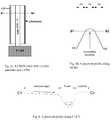
- FIG. 1illustrates a cross sectional view of a prior art small CMOS pixel.
- FIG. 2 aillustrates a simplified cross sectional view of an embodiment of a pixel with a nanowire structured photodetector with front side illumination.
- FIG. 2 billustrates an aspect of the embodiment illustrated in FIG. 2 a with a binary microlens on the NW structured photodetector.
- FIG. 3illustrates simplified cross section view of an embodiment of a pixel with a nanowire structured photodetector with backside illumination.
- FIG. 4illustrates an embodiment having a CMOS pixel with a nanowire and a vertical photogate (VPG).
- VPGvertical photogate
- FIG. 5 aillustrates an embodiment having a CMOS pixel with a n-type nanowire and a VPG.
- FIG. 5 billustrates a potential profile of the embodiment of FIG. 5 a along line A 1 -A 2 .
- FIG. 5 cillustrates an embodiment having a CMOS pixel with a p-type nanowire and a VPG.
- FIG. 5 dillustrates a potential profile of the embodiment of FIG. 5 c along line B 1 -B 2 .
- FIG. 6illustrates a potential profile of the embodiment of FIG. 4 along line C 1 -C 2 .
- FIG. 7 aillustrates an embodiment having a negative photogate bias and a gradual variation in the thickness of the dielectric cladding layer.
- FIG. 7 billustrates an embodiment having a negative photogate bias and a stepwise variation in the thickness of the dielectric cladding layer.
- FIG. 7 cillustrates an embodiment having a positive photogate bias and a gradual variation in the thickness of the dielectric cladding layer.
- FIG. 7 dillustrates an embodiment having a positive photogate bias and a stepwise variation in the thickness of the dielectric cladding layer.
- FIG. 8illustrates a cross section view of an embodiment with a dual photodiode structure in which the p doped NW is coated with an n+ epitaxial layer to form a p-n junction.
- FIG. 9illustrates an embodiment of a CMOS pixel with a nanowire structured photogate detector.
- FIG. 10illustrates an embodiment of a CMOS active pixel with nanowire structured p-i-n photodiodes and vertical photogates around the NW.
- FIG. 11illustrates another embodiment of a CMOS active pixel with nanowire structured p-i-n photodiodes and vertical photogates around the NW.
- FIG. 12illustrates an embodiments of a back-side illuminated image sensor.
- FIG. 13illustrates an embodiments of another back-side illuminated image sensor.
- VPG 1(VP Gate 1) The first vertical photogate VPG 2 (VP Gate 1) The second vertical photogate TX Gate Transfer gate RG Reset gate RD Reset drain Sub substrate Out Output NW (nw) Nanowire PG photogate I (i) Current n+, n ⁇ Semiconducting material with excess donors, n+ is heavily doped, n ⁇ is lightly doped p+, p ⁇ Semiconducting material with excess acceptors, p+ is heavily doped, p ⁇ is lightly doped
- Nanowirerefers to a structure that has a thickness or diameter of the order of several nanometers, for example, hundreds of nanometers or less and an unconstrained length.
- Nanowirescould include metallic (e.g., Ni, Pt, Au), semiconducting (e.g., Si, InP, GaN, etc.), and insulating (e.g., SiO 2 ,TiO 2 ) materials. Nanowires could exhibit aspect ratios (length-to-width ratio) of 100 or more. As such they could be referred to as 1-dimensional materials. Nanowires could have many interesting properties that are not observed in bulk or 3-dimensional (3-D) materials. This is because electrons in nanowires could be quantum confined laterally and thus occupy energy levels that could be different from the traditional continuum of energy levels or bands found in bulk materials. As a result, nanowires could have discrete values of electrical and optical conductance.
- the nanowireis upstanding (perpendicular to) and protruding from the substrate.
- the upstanding nanowirecould be on the front side of the substrate or at the back side of the substrate.
- the substrate of the embodiments hereintypically have electronic components and the nanowire photodiode.
- the upstanding nanowireis on the same side of the substrate where the electronic components are located, while in the back-side nanowire structure, the upstanding nanowire is located on the side of the substrate opposite to the side where the electronic components are located in or on the substrate.
- the CMOS pixel and nanowirecan be formed by using different materials, respectively.
- siliconcould be used to fabricate a CMOS image device.
- the nanowirecould be formed on the fabricated CMOS device by using group III-V or group II-VI materials, e.g., GaAS, GaN, GaP, InP, InN, InAs, CdTe, CdSe, ZnS, ZnSe, etc.
- a transfer gateis a switch or a transistor used in a pixel. The transfer gate's role is to transfer the charges from one side of a device to another. In some embodiments, the transfer gate is used to transfer the charges from the photodiode to the sense node (or floating diffusion).
- a reset gateis a gate switch used for resetting a device. In some embodiments, the device is the sense node which is formed by an n+ region. Reset means to restore to original voltage level set by a certain voltage. In some embodiments, the voltage of the reset drain (RD) is the voltage used as a reset level.
- a pinned photodiodeis a photodiode that includes a state that does not have a voltage variation.
- a conventional pinned photodiodeincludes a doped pinning layer at the surface of the active layer of the photodiode which depletes the mobile charges in the photodiode.
- the pinning layertypically pins the potential of the surface of the active layer of the photodiode to the potential of the substrate, typically ground level or zero volts. In this manner, the pinning layer reduces dark current from the surface of the active layer of the photodiode.
- silicon NWsare be grown using the vapor-liquid-solid (VLS) growth method.
- VLSvapor-liquid-solid
- a metal dropletcatalyzes the decomposition of a Si-containing source gas. Silicon atoms from the gas dissolves into the droplet forming a eutectic liquid. The eutectic liquid functions as a Si reservoir. As more silicon atoms enter into solution, the eutectic liquid becomes supersaturated in silicon, eventually causing the precipitation of Si atoms. Typically, the Si precipitates out of the bottom of the drop, resulting in bottom up growth of a Si—NW with the metal catalyst drop on top.
- goldis used as the metal catalyst for the growth of silicon NWs.
- Other metalsmay be used, including, but not limited to, Al, GA, In, Pt, Pd, Cu, Ni, Ag, and combinations thereof.
- Solid goldmay be deposited and patterned on silicon wafers using conventional CMOS technologies, such as sputtering, chemical vapor deposition (CVD), plasma enhanced chemical vapor deposition (PECVD), evaporation, etc. Patterning may be performed, for example, with optical lithography, electron-beam lithography, or any other suitable technique.
- the silicon wafercan then be heated, causing the gold to form droplets on the silicon wafer. Silicon and gold form a eutectic at 19% Au having a melting temperature at 363° C. That is, a liquid drop of Si—Au eutectic forms at 363° C., a moderate temperature suitable for the processing of silicon devices.
- the substrateshave a (111) orientation. Other orientations, however, may also be used, including, but not limited to (100).
- a common silicon source gas for NW productionis SiH 4 . Other gases, however, may be used including, but not limited to, SiCl 4 .
- NW growthmay be conducted, for example, with SiH 4 at pressures of 80-400 mTorr and temperatures in the range of 450-600° C. In some embodiments, the temperature is in a range of 470-540° C. Typically, lower partial pressures of SiH 4 result in the production of a higher percentage of vertical nanowires (NW).
- NWsmay be grown which are essentially round. In other embodiments, the NW are hexagonal.
- NW growthis conducted in a hot wall low pressure CVD reactor. After cleaning the Si substrates with acetone and isopropanol the samples may be dipped in a buffered HF solution to remove any native oxide. Successive thin Ga and Au metal layers (nominally 1-4 nm thick) may deposited on the substrates by thermal evaporation. Typically, the Ga layer is deposited before the Au layer. In an embodiment, after evacuating the CVD-chamber down to approximately 10 ⁇ 7 ton, the substrates can be heated up in vacuum to 600° C. to form metal droplets. The Si—NWs can be grown, for example, at a total pressure of 3 mbar using a 100 sccm flow of SiH4 (2% in a He mixture) in a temperature range from 500° C. to 700° C.
- the size and length of the Si—NWs grown with a Au—Ga catalystare relatively homogeneous, with most of the wires oriented along the four ⁇ 111> directions.
- Si—NWs grown with a pure Au catalystnucleate and grow with lengths and diameters of the NWs more randomly distributed.
- NWs grown with a Au—Ga catalysttend to have a taper along the axial direction.
- the tip diameters of NWs grown for a long timeare the same as those grown for a short time and are determined by the catalyst diameter.
- the footprints of the NWstend to increase during the course of the growth. This indicates that NW tapering is caused primarily by sidewall deposition (radial growth) of silicon.
- NWsmay be grown having a diameter at the foot (base) of 1500 nm, while the diameter of the tip may less than 70 nm over a length of 15 ⁇ m. Further, the NW diameter is a function of growth temperature. Higher growth temperatures result in NW with smaller diameters. For example, the average diameter of NWs grown with the Ga/Au catalyst at 600° C. is about 60 nm but the average diameter decreases down to about 30 nm for growth at 500° C. Additionally, the variation in diameters tends to narrow as deposition temperature is lowered.
- vertical NWsmay be grown. That is, nanowires which are essentially perpendicular to the substrate surface. Typically, not all NW will be perfectly vertical. That is, the NWs may be tilted at an angle to the surface other than 90 degrees. Commonly observed tilted NWs include, but are not limited to, the three 70.5°-inclined ⁇ 111> epitaxial growth directions and three additional 70.5°-inclined directions, which are rotated by 60°.
- the VLS processmay be used to grow doped NWs.
- a doping profile in the growing wirecan be produced.
- the NWcan be made p-type by adding diborane (B 2 H 2 ) or trimethyl borane (TMB) to the source gas.
- Other gases that add acceptor atoms to the silicon NWmay also be used.
- the NWcan be made n-type by adding PH 3 or AsH 3 to the source gas.
- Other gases that add donor atoms to the silicon NWmay also be used.
- Doping profiles which can be producedinclude but are not limited to, n-p-n, p-n-p, and p-i-n.
- VLS methodmay be used to grow NWs.
- Other methods or variationinclude, but are not limited to, (1) CVD, (2) reactive atmosphere, (3) Evaporation, (4) molecular beam epitaxy (MBE), (5) laser ablation, and (6) solution methods.
- a volatile gaseous silicon precursoris provided.
- Example silicon precursor gasesinclude SiH 4 and SiCl 4 .
- CVDmay be used for epitaxial growth.
- dopingcan be accomplished by adding volatile doping precursors to the silicon precursor.
- Annealing in a reactive atmospherecomprises heating the substrate in a gas that reacts with the substrate. For example, if silicon is annealed in an atmosphere including hydrogen, the hydrogen locally reacts with the silicon substrate, forming SiH 4 .
- the SiH 4can then react with the catalyst metal drop, thereby initiating NW growth. This growth process can be used for non-CMOS processes.
- a SiO 2 sourceis heated under conditions that result in the production of SiO gas.
- SiO gasadsorbs on the metal catalyst droplets, it forms Si and SiO 2 .
- This methodmay also be performed without a metal catalyst drop. Absent a metal catalyst, SiO 2 has been observed to catalyze silicon NW growth.
- a high purity silicon sourceis heated until Si atoms evaporate. A gaseous beam of Si directed toward the substrate. The gaseous silicon atoms adsorb onto and dissolve into the metal droplet, thereby initiating growth of NWs.
- a laser beamis aimed at source which includes both silicon and catalyst atoms.
- the ablated atomscool by colliding with inert gas molecules and condense to form droplets with the same composition as the original target. That is, droplets having both silicon and catalyst atoms.
- the laser ablation methodmay also be performed with a target consisting essentially of pure silicon.
- Solution based techniquestypically use organic fluids. Specifically, the organic fluids generally comprise highly pressurized supercritical organic fluids enriched with a silicon source and catalyst particles. At a reaction temperature above the metal-silicon eutectic, the silicon precursor decomposes, forming an alloy with the metal. Upon supersaturation, silicon precipitates out, growing the NW.
- Nanowire growth techniquesare all bottom up techniques. Nanowires, however may also be fabricated with top down techniques.
- Top down techniquestypically involve patterning and etching a suitable substrate, for example silicon. Patterning can be accomplished via lithography, for, example, electron beam lithography, nanosphere lithography and nanoprint lithography. Etching may be performed either dry or wet. Dry etching techniques include, but are not limited to, reactive ion etching. Wet etching may be performed with either standard etches or via the metal-assisted etching process. In the metal-assisted etching process, Si is et-chemically etched, with the Si dissolution reaction being catalyzed by the presence of a noble metal that is added as a salt to the etching solution.
- a nanowireabsorbs a certain selective bandwidth of light energy depending on its dimensions and its design parameters such as a diameter, length and refractive index of its core and cladding layers. Unabsorbed light energy travels along the nanowire as in a waveguide.
- the nanowirecould be used as a color selective filter device in an imaging device.
- the nanowire structured photodetectorcould be constructed as a color sensitive photo sensor. By extending this feature, a color information gathering pixel array could be formed.
- FIG. 2shows a simplified cross section view of one pixel of a focal plane array of many such cells formed in an imaging device.
- Each pixelincludes a readout circuit 100 formed on a semiconductor substrate 101 with metal lines 103 above the substrate.
- a nanowire structured photodetector 102is formed standing up from the substrate. Photo absorption takes place along the length of the nanowire structured photodetector 102 .
- the output of the nanowire structured photodetector 102can be connected to the readout circuit 100 located in the substrate. Since the footprint of the nanowire structured photodetector 102 is small, more than one nanowire structured photodetector 102 can be formed in a pixel.
- the role of the long vertical structure of the nanowire structured photodetector 102is to absorb a certain bandwidth of light energy and generate a corresponding electrical signal and/or to guide the unabsorbed light energy to the substrate diode with minimum loss, thus performing as a waveguide.
- an optical couplere.g., a lens
- a micro lensmay be used as a coupler.
- the microlensmay be, but not limited to, a spherical ball lens. The coupling efficiency of a spherical ball lens is typically higher than 90%.
- a binary microlensmay be used as shown in FIG. 2 b.
- FIG. 3shows a simplified cross section view of a pixel which has a nanowire structured photodetector at the back side of a thinned semiconductor substrate.
- the nanowire 109generates photo charges by absorbing light energy in a certain bandwidth and dumping the charges into the thinned substrate. The charges are then collected by readout circuits 100 in the thinned substrate using an electrical field. Also, the nanowire guides and couples unabsorbed light into the substrate 108 .
- An advantage of employing a nanowire structured photodetector at the back side of the substrate 108is the ease of fabricating the nanowires. When forming nanowires at the front side, it is necessary to remove the thick dielectric layers 104 illustrated in FIG. 2 in a region where the nanowire is supposed to be constructed.
- the embodiment disclosed in FIG. 3could be made without this removal step.
- the nanowiremay fabricated without modifying front side structure of the CMOS devices.
- This embodimentincludes both front side metal and insulating layers 106 and backside metal and insulating layers 107 .
- a micro lens of an optical coupler 105may be coupled to the nanowire 109 .
- a nanowire structured semiconductorcould be configured in a variety of photodetector configurations. These configurations include: a photo conductor, a photodiode, or a photogate device.
- a photo conductoris a photo sensitive device whose resistivity varies as a function of incident light.
- a photodiodeis a p-n diode or a p-i-n diode which generates electron-hole pairs as a photo charge.
- a photogate deviceis a MOS (metal-oxide-semiconductor) device with a biased gate that creates a potential well in the semiconductor and accumulates photo charge in the potential well.
- MOSmetal-oxide-semiconductor
- FIG. 4shows a cross sectional view of a CMOS pixel with a nanowire structured photogate device.
- the NWis formed of an n-type semiconductor with a dielectric cladding layer and a vertical gate.
- the role of the vertical gate surrounding the NWis to deplete the NW and create a potential well at the NW core as shown in FIG. 5 b by applying a slight negative bias voltage to the NW photogate. Further increase of the negative bias voltage would invert the surface region of the NW to p+ because holes are accumulated in the surface region due to the negative photogate bias.
- the NWacts similarly to a pinned photodiode, however, without impurity doping.
- a positive bias voltagemay be applied to deplete the nanowire.
- a photogate biasis not needed for depletion.
- a negative biasmay be applied to produce a surface pinning effect.
- a vertical photogate surrounding the nanowire structured photodetectormay produce several benefits. It is known that the surface of a semiconductor, including silicon, has defects due to dangling bonds of the interface atoms. These defects form defect states within the energy bandgap in a semiconductor and result in leakage or dark current through the thermal generation process. Without the photogate bias, the NW could have a very large dark current generated from its surface region. This is because the surface to volume ratio of the NW is very large compared to a conventional substrate device. Thus, a photogate bias voltage may help suppress the dark current by electrically passivating the nanowire surface. The surface of the nanowire may also be passivated by chemically treating the surface to remove all dangling bonds.
- Such a methodcan be implemented for a silicon nanowire, for example, by the use of atomic layer deposition (ALD) of a very thin layer of material such as LaAlO3, GdScO 3 , LaScO 3 , etc.
- ALDatomic layer deposition
- the surfacemay be chemically treated with HfO 2 through the use of MOCVD or sputtering.
- Another problem could be caused by the NW surfaceis that photo generated carriers could have a short lifetime due to the recombination process occurring at the defect states at NW surface. Passivating the NW surface by applying the bias voltage to the surrounding photogate is therefore beneficial because it helps reduce the dark current and enhances the photo carrier lifetime, resulting in better quantum efficiency.
- the electrical potential of the NW coreis not constant along the axial direction C 1 -C 2 of the NW. This is because the top end of the NW is open and influenced most by the negative gate bias while the bottom end of the NW is connected to the N-well that has positive bias voltage during reset and holds the bias after reset. As a result, the closer to the top of the nanowire, the more negative the bias. The closer to the bottom of the NW, the more positive bias established in the NW. As a result, a potential gradient is established along the axial direction of the NW as shown in FIG. 6 . This gradient causes photo charges generated in the NW to drift into the potential well in the substrate diode.
- a p-type NWis used.
- a positive bias voltagecan be applied to the photogate that surrounds the NW as shown in FIG. 5 c .
- the surface of the p-type NWbecomes depleted with a slight positive photogate bias. Further increase of the photogate bias would deplete the entire region of the NW, i.e., from the surface to the core of the NW.
- a potential profile for this aspect of the NWis shown in FIG. 5 d.
- a p-n junction diodemay be formed between the p-type substrate and n-well region.
- a p+ layercovers the n-well surface except the NW junction. This p+ shape allows receiving the photo charges coming from the NW and suppress the dark current due to the surface states of the substrate. Since light passing through the NW can illuminate the substrate diode, photo charges are generated in the substrate diode and collected in the potential well. Consequently, the potential well collects the charges both from the NW and the substrate diode.
- this embodimentcan enhance the quantum efficiency by utilizing most of the incident photons.
- the n-well of the substrate photo diodeis lightly doped so that the n-region can be easily depleted with a low bias voltage.
- the depleted n-wellis preferred for a complete charge transfer from the substrate diode to the sense node when the transfer gate is turned on. Complete charge transfer allows for a low noise readout of the photo charges similar to CCD devices.
- the sense nodeis formed with n+ diffusion in the substrate.
- the sense nodeis connected to an amplifying transistor, e.g., a transistor configured as a source follower transistor.
- a select switch transistormay be used to control the connection of the amplifier output to an output node.
- a reset transistormay also be connected to the sense node so that sense node is biased to VDD when the reset gate is activated.
- the transfer gateis activated, the n-well is electrically connected to the sense node. Then, the n-well becomes positively biased and a potential gradient in the NW is established between the n-well potential and the vertical photogate bias voltage.
- further potential gradient along the axial directioncan be obtained by gradually or stepwise varying the thickness of dielectric cladding layer as shown in FIG. 7 a and FIG. 7 b , respectively. Since the potential drop across the dielectric layer is proportional to the thickness of the layer, the potential of the NW varies gradually along the axial direction. This potential gradient is beneficial for efficient collection of the photo generated carriers and to enhance the carrier lifetime. This is because the axial electric field helps remove thermally generated carriers from the NW region and therefore electron-hole recombination probability is reduced.
- a p-type NWis used.
- a potential gradient along the axial NW directioncan be established by gradually or stepwise varying the thickness of the cladding layer as shown in FIG. 7 c and FIG. 7 d , respectively.
- FIG. 8shows a cross section view of a dual photodiode structure in which the p doped NW is coated with an n+ epitaxial layer to form a p-n junction.
- the NWcould be doped and the coating could be en epitaxial p+ layer to form a p-n junction.
- FIG. 8there are two photodiodes per pixel, one is a NW diode and the other is a substrate diode.
- the NW phtodiodeis formed with a p ⁇ , n ⁇ , or intrinsic type semiconductor.
- a n+ layercovers the NW surface, forming a p-n diode or a p-i-n diode.
- a n ⁇ diodeis lightly doped so that the n ⁇ region can be easily depleted with a low bias voltage.
- Photo chargesare integrated in both of photodiodes at the same time, but in separate potential wells. This is because the photodiodes are separated by a p+ layer to avoid interaction between the two photodiodes.
- the readout circuit for the NWhas a 3-T configuration, e.g., a rest transistor, n source follower amplifier, and a select switch (not shown in FIG. 8 ).
- the second readout circuit for the substrate diodeis based on a 4-T configuration, e.g., a transfer gate, a reset transistor, a source follower transistor, and a select switch. It is also possible that the 4-T configuration be replaced with a 3-T configuration by removing the transfer gate.
- FIG. 9shows an embodiment of a CMOS pixel with a nanowire structured photogate detector.
- This embodimentincludes two vertical photogates (VP Gate 1 , VP Gate 2 ) around the NW, a substrate photodiode, and a readout circuit.
- the readout circuitincludes a transfer gate (TX), a reset gate (RG), a source follower transistor, and a pixel select switch.
- the buffer amplifier in FIG. 9represents the source follower transistor and the pixel select switch for simplification.
- an upstanding nanowireis formed with an n ⁇ , i.e. lightly doped n-type or an intrinsic semiconductor so that the NW can be easily depleted with a low negative bias voltage from VP Gate 1 .
- a negative bias voltage from the vertical photogate VP Gate 1could cause accumulation of holes at the surface of the NW to suppress dark current due to the surface states of the NW as illustrated in the FIG. 5 b.
- the second vertical photogate VP Gate 2could be an on/off switch. This switch could be configured to separate the photo charges generated in the NW from the photo charges integrated in the substrate photodiode. Photo charges are integrated in both the NW and substrate photodiode at the same time. The photo charges, however, are integrated in separate potential wells because the off-state of the second photogate VP Gate 2 forms a potential barrier between the NW and substrate photodiode. In this manner, signal from the NW and the substrate photodiodes do not mix together. These two photodiodes can be used to collect charges created by radiations of different wavelengths.
- the vertical photogates implemented in this embodimentallow the ability to easily modify the potential profile in the NW without using a complicated ion implantation process.
- the conventional photogate pixelsuffers from very poor quantum efficiency and poor blue response.
- the conventional photogateis normally made of polysilicon which covers the top surface of the substrate photodiode and absorbs short wavelengths near the blue light, thereby reducing the blue light reaching the photodiode.
- the vertical photogatein contrast, does not block the light path. This is because the vertical photogate (VPG) does not lie laterally across the photodiode to control the potential profile in the semiconductor.
- the aperture size of the image sensorbecomes comparable to the wavelength of light propagated.
- QEquantum efficiency
- the NW pixel of the present embodimentuses a two step process to read out the signals separately between the NW and substrate photodiodes.
- the first stepthe signal charges in the substrate photodiodes are read out.
- the n ⁇ region in the substrateis depleted.
- the second stepthe second photogate VP Gate 2 may be first turned on.
- the signal charges in the NWare read out.
- a device of this embodimentmay be operated in a “snapshot” operation.
- a “snapshot” operationpreferably all of the photogates VP gate 2 in the pixel array are turned on or off at the same time. The same could be true for the transfer gate TX.
- the second photogate VP Gates 2are all connected with a global connection. Further, all the transfer gates TX are connected with a second global connection.
- FIG. 10 and FIG. 11show embodiments of CMOS active pixels with nanowire structured p-i-n photodiodes and vertical photogates around the NW.
- a NWcan be configured to have an axial type p-i-n photodiode by having p+ and n ⁇ at each end, respectively.
- a NWcan have a coaxial type p-i-n configuration as shown in FIG. 11 .
- a NWcan have one or more vertical photogates comprising epitaxially grown layers such as conductive layers and metal layers.
- the pixelcould include two photodiodes, a NW photodiode and a substrate photodiode.
- This embodimentalso includes two vertical photogates (VP Gate 1 , VP Gate 2 ), a transfer gate (TX) and a reset gate (RG).
- both of the photodiodesare lightly doped. This is because a lightly doped region can be easily depleted with a low bias voltage.
- both of the photodiodesare n ⁇ .
- the NW pixelcould be configured so that both of photodiodes are p ⁇ .
- the surface region of the substrate photodiodecould be prone to defects due to process induced damage caused during fabrication and to lattice stress associated with the upstanding NW. These defects may serve as a source for dark current.
- a shallow p+ regionis fabricated on top of the n ⁇ photodiode in the substrate.
- the substrateis connected to ground, that is, zero voltage.
- the reset drainis preferably doped n+ and is positively biased.
- the transfer gate TX and reset gateare on, the n ⁇ region in the substrate becomes positively biased. This reset operation results in the n ⁇ region being depleted due to a reverse bias condition between the p substrate and n ⁇ region.
- the transfer gate TX and reset gate RGare off, the n ⁇ region retains its positive bias, forming a floating capacitor with respect to the p-sub region.
- the first vertical photogate VP Gate 1could be configured to control the potential in the NW so that a potential gradient can be formed between the NW photodiode and the substrate photodiode. In this way, photo charges in the NW can drift quickly to the n ⁇ region of the substrate during readout.
- the second vertical photogate VP Gate 2could be an on/off switch.
- FIG. 12 and FIG. 13show embodiments of back-side illuminated image sensors.
- the NWcould be formed at the back side of a p-substrate.
- the substratemay be thinned by removing semiconductor substrate material over the area containing the pixel array.
- a p-substratecan be thinned to a thickness between 3 and 50 microns, more preferably, between 6 and 20 microns.
- the substrate photodiodecould now get all of its light from the back-side and not from the side containing all the metal lines as in conventional image sensors.
- the front sidecould include a 4-T readout circuit including a transfer gate TX, a reset switch with a reset gate RG, a source follower amplifier, and a select switch.
- the readout circuitsalso could be configured as a 3-T pixel circuit including, a reset switch with a reset gate RG, a source follower amplifier, and a select switch.
- a substrate photodiodemay be formed with a shallow p+ layer as shown in FIG. 12 and FIG. 13 . The purpose of having p+ at both sides of the substrate is to suppress dark current.
- a buried p layercould be placed underneath the n+ diffusion layer to block incoming charge flow from the backside and deflect the charges toward the n ⁇ region.
- doping of the buried p layeris higher than that of the p ⁇ substrate, but not as high as that of the p+ layer.
- the front side photodiodeis not for photo absorption, but rather for collecting the charges coming from the NW and from the backside p ⁇ substrate where photon absorption takes place.
- the NWcould have a dielectric layer (cladding layer) surrounding the NW and two vertical photogates, one for the switch and the other for controlling the potential in the NW.
- a two step processis used to read out the signal charges separately from each of the photodiodes.
- the first stepwould be to read out the charges from the substrate diode at the front side. Immediately after this, by turning on the VP Gate 1 , the charges from the NW would be read out.
- the embodiments of FIG. 12 and FIG. 13should have a shallow p+ layer at the backside substrate with a hole in the center so that the p+ layer does not block the charges coming from the backside NW.
- at the front sidethere should be a lightly doped n-well or n ⁇ layer underneath the shallow p+ layer so that n-well could be easily depleted.
- FIG. 13shows an alternative embodiment of a backside illuminated CMOS pixel.
- the p+ layerinstead of having vertical photogate for the NW, the p+ layer could be coated at the outer shell of the NW to help create a built-in electric field in the NW. With this configuration, photo charges can easily drift in the upward direction.
- the features of the back-side illumination CMOS pixelare similar to those of the pixel of FIG. 12 .
Landscapes
- Solid State Image Pick-Up Elements (AREA)
- Transforming Light Signals Into Electric Signals (AREA)
- Chemical & Material Sciences (AREA)
- Engineering & Computer Science (AREA)
- Materials Engineering (AREA)
- Nanotechnology (AREA)
- Light Receiving Elements (AREA)
Abstract
Description
| TABLE 1 | |
| Symbol | Element |
| VPG 1 (VP Gate 1) | The first vertical photogate |
| VPG 2 (VP Gate 1) | The second vertical photogate |
| TX Gate | Transfer gate |
| RG | Reset gate |
| RD | Reset drain |
| Sub | substrate |
| Out | Output |
| NW (nw) | Nanowire |
| PG | photogate |
| I (i) | Current |
| n+, n− | Semiconducting material with excess donors, |
| n+ is heavily doped, n− is lightly doped | |
| p+, p− | Semiconducting material with excess acceptors, |
| p+ is heavily doped, p− is lightly doped | |
Claims (25)
Priority Applications (23)
| Application Number | Priority Date | Filing Date | Title |
|---|---|---|---|
| US12/633,305US8299472B2 (en) | 2009-12-08 | 2009-12-08 | Active pixel sensor with nanowire structured photodetectors |
| US12/945,492US9515218B2 (en) | 2008-09-04 | 2010-11-12 | Vertical pillar structured photovoltaic devices with mirrors and optical claddings |
| TW102149110ATW201432894A (en) | 2009-12-08 | 2010-12-08 | Active pixel sensor with nanowire structured photodetector |
| PCT/US2010/059501WO2011072032A1 (en) | 2009-12-08 | 2010-12-08 | Active pixel sensor with nanowire structured photodetectors |
| JP2012543250AJP5576943B2 (en) | 2009-12-08 | 2010-12-08 | Active pixel sensor with photodetector of nanowire structure |
| TW099142973ATWI427781B (en) | 2009-12-08 | 2010-12-08 | Active pixel sensor with nanowire structured photodetector |
| US13/106,851US9082673B2 (en) | 2009-10-05 | 2011-05-12 | Passivated upstanding nanostructures and methods of making the same |
| US13/543,556US8766272B2 (en) | 2009-12-08 | 2012-07-06 | Active pixel sensor with nanowire structured photodetectors |
| US13/925,429US9304035B2 (en) | 2008-09-04 | 2013-06-24 | Vertical waveguides with various functionality on integrated circuits |
| US14/293,164US9490283B2 (en) | 2009-11-19 | 2014-06-02 | Active pixel sensor with nanowire structured photodetectors |
| JP2014138265AJP2014241413A (en) | 2009-12-08 | 2014-07-04 | Active pixel sensor with nanowire structured photodetectors |
| US14/503,598US9410843B2 (en) | 2008-09-04 | 2014-10-01 | Nanowire arrays comprising fluorescent nanowires and substrate |
| US14/516,162US20160111562A1 (en) | 2008-09-04 | 2014-10-16 | Multispectral and polarization-selective detector |
| US14/516,402US20160111460A1 (en) | 2008-09-04 | 2014-10-16 | Back-lit photodetector |
| US14/632,739US9601529B2 (en) | 2008-09-04 | 2015-02-26 | Light absorption and filtering properties of vertically oriented semiconductor nano wires |
| US14/704,143US20150303333A1 (en) | 2008-09-04 | 2015-05-05 | Passivated upstanding nanostructures and methods of making the same |
| US14/705,380US9337220B2 (en) | 2008-09-04 | 2015-05-06 | Solar blind ultra violet (UV) detector and fabrication methods of the same |
| US15/057,153US20160178840A1 (en) | 2008-09-04 | 2016-03-01 | Optical waveguides in image sensors |
| US15/082,514US20160211394A1 (en) | 2008-11-13 | 2016-03-28 | Nano wire array based solar energy harvesting device |
| US15/090,155US20160216523A1 (en) | 2008-09-04 | 2016-04-04 | Vertical waveguides with various functionality on integrated circuits |
| US15/093,928US20160225811A1 (en) | 2008-09-04 | 2016-04-08 | Nanowire structured color filter arrays and fabrication method of the same |
| US15/149,252US20160254301A1 (en) | 2008-09-04 | 2016-05-09 | Solar blind ultra violet (uv) detector and fabrication methods of the same |
| US15/225,264US20160344964A1 (en) | 2008-09-04 | 2016-08-01 | Methods for fabricating and using nanowires |
Applications Claiming Priority (1)
| Application Number | Priority Date | Filing Date | Title |
|---|---|---|---|
| US12/633,305US8299472B2 (en) | 2009-12-08 | 2009-12-08 | Active pixel sensor with nanowire structured photodetectors |
Related Parent Applications (2)
| Application Number | Title | Priority Date | Filing Date |
|---|---|---|---|
| US12/633,323Continuation-In-PartUS8735797B2 (en) | 2008-09-04 | 2009-12-08 | Nanowire photo-detector grown on a back-side illuminated image sensor |
| US12/982,269Continuation-In-PartUS9299866B2 (en) | 2008-09-04 | 2010-12-30 | Nanowire array based solar energy harvesting device |
Related Child Applications (2)
| Application Number | Title | Priority Date | Filing Date |
|---|---|---|---|
| US12/633,313Continuation-In-PartUS20100148221A1 (en) | 2008-09-04 | 2009-12-08 | Vertical photogate (vpg) pixel structure with nanowires |
| US13/543,556ContinuationUS8766272B2 (en) | 2008-09-04 | 2012-07-06 | Active pixel sensor with nanowire structured photodetectors |
Publications (2)
| Publication Number | Publication Date |
|---|---|
| US20110133060A1 US20110133060A1 (en) | 2011-06-09 |
| US8299472B2true US8299472B2 (en) | 2012-10-30 |
Family
ID=44081097
Family Applications (3)
| Application Number | Title | Priority Date | Filing Date |
|---|---|---|---|
| US12/633,305Expired - Fee RelatedUS8299472B2 (en) | 2008-09-04 | 2009-12-08 | Active pixel sensor with nanowire structured photodetectors |
| US13/543,556Expired - Fee RelatedUS8766272B2 (en) | 2008-09-04 | 2012-07-06 | Active pixel sensor with nanowire structured photodetectors |
| US14/293,164Expired - Fee RelatedUS9490283B2 (en) | 2008-09-04 | 2014-06-02 | Active pixel sensor with nanowire structured photodetectors |
Family Applications After (2)
| Application Number | Title | Priority Date | Filing Date |
|---|---|---|---|
| US13/543,556Expired - Fee RelatedUS8766272B2 (en) | 2008-09-04 | 2012-07-06 | Active pixel sensor with nanowire structured photodetectors |
| US14/293,164Expired - Fee RelatedUS9490283B2 (en) | 2008-09-04 | 2014-06-02 | Active pixel sensor with nanowire structured photodetectors |
Country Status (4)
| Country | Link |
|---|---|
| US (3) | US8299472B2 (en) |
| JP (2) | JP5576943B2 (en) |
| TW (2) | TW201432894A (en) |
| WO (1) | WO2011072032A1 (en) |
Cited By (25)
| Publication number | Priority date | Publication date | Assignee | Title |
|---|---|---|---|---|
| US20110180894A1 (en)* | 2008-09-04 | 2011-07-28 | Qunano Ab | Nanostructured photodiode |
| US20120298843A1 (en)* | 2009-12-08 | 2012-11-29 | Zena Technologies, Inc. | Nanowire photo-detector grown on a back-side illuminated imager sensor |
| US8514411B2 (en) | 2009-05-26 | 2013-08-20 | Zena Technologies, Inc. | Determination of optimal diameters for nanowires |
| US8546742B2 (en) | 2009-06-04 | 2013-10-01 | Zena Technologies, Inc. | Array of nanowires in a single cavity with anti-reflective coating on substrate |
| US8710488B2 (en) | 2009-12-08 | 2014-04-29 | Zena Technologies, Inc. | Nanowire structured photodiode with a surrounding epitaxially grown P or N layer |
| US8742406B1 (en)* | 2011-02-16 | 2014-06-03 | Iowa State University Research Foundation, Inc. | Soft lithography microlens fabrication and array for enhanced light extraction from organic light emitting diodes (OLEDs) |
| US8748799B2 (en) | 2010-12-14 | 2014-06-10 | Zena Technologies, Inc. | Full color single pixel including doublet or quadruplet si nanowires for image sensors |
| US8766272B2 (en)* | 2009-12-08 | 2014-07-01 | Zena Technologies, Inc. | Active pixel sensor with nanowire structured photodetectors |
| US8765609B2 (en)* | 2012-07-25 | 2014-07-01 | Power Integrations, Inc. | Deposit/etch for tapered oxide |
| US8791470B2 (en) | 2009-10-05 | 2014-07-29 | Zena Technologies, Inc. | Nano structured LEDs |
| US8835905B2 (en) | 2010-06-22 | 2014-09-16 | Zena Technologies, Inc. | Solar blind ultra violet (UV) detector and fabrication methods of the same |
| US8866065B2 (en) | 2010-12-13 | 2014-10-21 | Zena Technologies, Inc. | Nanowire arrays comprising fluorescent nanowires |
| US8890271B2 (en) | 2010-06-30 | 2014-11-18 | Zena Technologies, Inc. | Silicon nitride light pipes for image sensors |
| US8889455B2 (en) | 2009-12-08 | 2014-11-18 | Zena Technologies, Inc. | Manufacturing nanowire photo-detector grown on a back-side illuminated image sensor |
| US9000353B2 (en) | 2010-06-22 | 2015-04-07 | President And Fellows Of Harvard College | Light absorption and filtering properties of vertically oriented semiconductor nano wires |
| US9082673B2 (en) | 2009-10-05 | 2015-07-14 | Zena Technologies, Inc. | Passivated upstanding nanostructures and methods of making the same |
| US9299866B2 (en) | 2010-12-30 | 2016-03-29 | Zena Technologies, Inc. | Nanowire array based solar energy harvesting device |
| US9304035B2 (en) | 2008-09-04 | 2016-04-05 | Zena Technologies, Inc. | Vertical waveguides with various functionality on integrated circuits |
| US20160111460A1 (en)* | 2008-09-04 | 2016-04-21 | Zena Technologies, Inc. | Back-lit photodetector |
| US9343490B2 (en) | 2013-08-09 | 2016-05-17 | Zena Technologies, Inc. | Nanowire structured color filter arrays and fabrication method of the same |
| US9406709B2 (en) | 2010-06-22 | 2016-08-02 | President And Fellows Of Harvard College | Methods for fabricating and using nanowires |
| US9429723B2 (en) | 2008-09-04 | 2016-08-30 | Zena Technologies, Inc. | Optical waveguides in image sensors |
| US9478685B2 (en) | 2014-06-23 | 2016-10-25 | Zena Technologies, Inc. | Vertical pillar structured infrared detector and fabrication method for the same |
| US9515218B2 (en) | 2008-09-04 | 2016-12-06 | Zena Technologies, Inc. | Vertical pillar structured photovoltaic devices with mirrors and optical claddings |
| US10840282B2 (en) | 2015-10-21 | 2020-11-17 | Ams Sensors Singapore Pte. Ltd. | Demodulation pixel devices, arrays of pixel devices and optoelectronic devices incorporating the same |
Families Citing this family (29)
| Publication number | Priority date | Publication date | Assignee | Title |
|---|---|---|---|---|
| KR101176545B1 (en)* | 2006-07-26 | 2012-08-28 | 삼성전자주식회사 | Method for forming micro-lens and image sensor comprising micro-lens and method for manufacturing the same |
| US8507840B2 (en) | 2010-12-21 | 2013-08-13 | Zena Technologies, Inc. | Vertically structured passive pixel arrays and methods for fabricating the same |
| WO2012035243A1 (en)* | 2010-09-14 | 2012-03-22 | Commissariat A L'energie Atomique Et Aux Energies Alternatives | Nanowire-based optoelectronic device for light emission |
| WO2013130620A1 (en)* | 2012-02-27 | 2013-09-06 | Arturo Ayon | Hyperlens and method of manufacture |
| WO2014028380A2 (en)* | 2012-08-13 | 2014-02-20 | President And Fellows Of Harvard College | Multispectral imaging using silicon nanowires |
| US9112087B2 (en)* | 2012-09-16 | 2015-08-18 | Shalom Wretsberger | Waveguide-based energy converters, and energy conversion cells using same |
| US10032951B2 (en) | 2013-04-04 | 2018-07-24 | Hamamatsu Photonics K.K. | Semiconductor photosensor for infrared radiation |
| US11791432B2 (en)* | 2013-05-22 | 2023-10-17 | W&Wsens Devices, Inc. | Microstructure enhanced absorption photosensitive devices |
| WO2015088281A1 (en)* | 2013-12-13 | 2015-06-18 | 주식회사 비욘드아이즈 | Unit pixel for image sensor comprising contact pad connected to light receiving portion |
| KR101626121B1 (en) | 2013-12-13 | 2016-06-13 | 주식회사 비욘드아이즈 | Unit Pixel of Image Sensor |
| US9812603B2 (en)* | 2014-05-30 | 2017-11-07 | Klaus Y. J. Hsu | Photosensing device with graphene |
| US9812604B2 (en)* | 2014-05-30 | 2017-11-07 | Klaus Y. J. Hsu | Photosensing device with graphene |
| WO2016145220A1 (en)* | 2015-03-10 | 2016-09-15 | The Regents Of The University Of California | Monolithic thin film elements and performance electronics, solar powered systems and fabrication |
| TWI591809B (en) | 2015-08-04 | 2017-07-11 | 國立交通大學 | Light sensing device and its application |
| US9936151B2 (en)* | 2015-10-16 | 2018-04-03 | Capsovision Inc | Single image sensor for capturing mixed structured-light images and regular images |
| FR3063564B1 (en)* | 2017-03-06 | 2021-05-28 | Isorg | INTEGRATED FINGERPRINT SENSOR IN A DISPLAY SCREEN |
| EP3759653B1 (en)* | 2018-03-02 | 2025-06-25 | AIstorm, Inc. | Charge domain mathematical engine and method |
| FR3078826B1 (en)* | 2018-03-07 | 2022-01-14 | St Microelectronics Crolles 2 Sas | VERTICAL PHOTODIODE |
| KR102070499B1 (en)* | 2018-04-11 | 2020-01-29 | 주식회사 크레파스테크놀러지스 | Silicon structure capable of controlling photo-reactive property |
| JP7103027B2 (en)* | 2018-07-30 | 2022-07-20 | 富士通株式会社 | Compound semiconductor equipment, manufacturing method of compound semiconductor equipment, power generation equipment and power supply equipment |
| WO2020041651A1 (en) | 2018-08-23 | 2020-02-27 | Raytheon Company | Per-pixel detector bias control |
| FR3091413B1 (en)* | 2018-12-28 | 2022-06-24 | Aledia | Optoelectronic device with micrometric or nanometric light-emitting diode surmounted by an optical lens |
| EP3709360A1 (en)* | 2019-03-13 | 2020-09-16 | Koninklijke Philips N.V. | Photodetector for imaging applications |
| CN109950359A (en)* | 2019-03-29 | 2019-06-28 | 中国科学院上海技术物理研究所 | A kind of enhanced low-dimensional nano-detector using hafnium dioxide passivation and preparation method |
| TWI703716B (en)* | 2019-11-08 | 2020-09-01 | 精準基因生物科技股份有限公司 | Image sensor |
| US11561132B2 (en)* | 2020-06-04 | 2023-01-24 | Raytheon Company | Per-pixel detector bias control |
| CN114530465A (en)* | 2020-11-23 | 2022-05-24 | 联华电子股份有限公司 | Image sensor device and method of making the same |
| JP2022146934A (en) | 2021-03-22 | 2022-10-05 | 三星電子株式会社 | image sensor |
| EP4099387A3 (en) | 2021-06-01 | 2023-04-05 | Samsung Electronics Co., Ltd. | Image sensor including a transistor with a vertical channel and a method of manufacturing the same |
Citations (218)
| Publication number | Priority date | Publication date | Assignee | Title |
|---|---|---|---|---|
| US1918848A (en) | 1929-04-26 | 1933-07-18 | Norwich Res Inc | Polarizing refracting bodies |
| US4017332A (en) | 1975-02-27 | 1977-04-12 | Varian Associates | Solar cells employing stacked opposite conductivity layers |
| US4827335A (en) | 1986-08-29 | 1989-05-02 | Kabushiki Kaisha Toshiba | Color image reading apparatus with two color separation filters each having two filter elements |
| US4880613A (en) | 1987-01-12 | 1989-11-14 | Sumitomo Electric Industries, Ltd. | Light emitting element comprising diamond and method for producing the same |
| US4896941A (en) | 1985-04-27 | 1990-01-30 | Doryokuro Kakunenryo Kaihatsu Jigyodan | Image-transmitting fiber |
| US4950625A (en) | 1988-06-13 | 1990-08-21 | Sumitomo Electric Industries, Ltd. | Diamond laser crystal and method manufacturing the same |
| US4972244A (en) | 1988-06-16 | 1990-11-20 | Commissariat A L'energie Atomique | Photodiode and photodiode array on a II-VI material and processes for the production thereof |
| US4971928A (en) | 1990-01-16 | 1990-11-20 | General Motors Corporation | Method of making a light emitting semiconductor having a rear reflecting surface |
| US5096520A (en) | 1990-08-01 | 1992-03-17 | Faris Sades M | Method for producing high efficiency polarizing filters |
| US5124543A (en) | 1989-08-09 | 1992-06-23 | Ricoh Company, Ltd. | Light emitting element, image sensor and light receiving element with linearly varying waveguide index |
| US5272518A (en) | 1990-12-17 | 1993-12-21 | Hewlett-Packard Company | Colorimeter and calibration system |
| US5311047A (en) | 1988-11-16 | 1994-05-10 | National Science Council | Amorphous SI/SIC heterojunction color-sensitive phototransistor |
| US5347147A (en) | 1990-11-28 | 1994-09-13 | Jones Barbara L | Light emitting diamond device |
| US5362972A (en) | 1990-04-20 | 1994-11-08 | Hitachi, Ltd. | Semiconductor device using whiskers |
| US5401968A (en) | 1989-12-29 | 1995-03-28 | Honeywell Inc. | Binary optical microlens detector array |
| US5449626A (en) | 1991-12-27 | 1995-09-12 | Hezel; Rudolf | Method for manufacture of a solar cell |
| US5602661A (en) | 1993-02-17 | 1997-02-11 | Hoffmann-La Roche Inc. | Optical component |
| US5612780A (en) | 1996-06-05 | 1997-03-18 | Harris Corporation | Device for detecting light emission from optical fiber |
| US5723945A (en) | 1996-04-09 | 1998-03-03 | Electro Plasma, Inc. | Flat-panel display |
| US5747796A (en) | 1995-07-13 | 1998-05-05 | Sharp Kabushiki Kaisha | Waveguide type compact optical scanner and manufacturing method thereof |
| US5767507A (en) | 1996-07-15 | 1998-06-16 | Trustees Of Boston University | Polarization sensitive photodetectors and detector arrays |
| US5798535A (en) | 1996-12-20 | 1998-08-25 | Motorola, Inc. | Monolithic integration of complementary transistors and an LED array |
| US5853446A (en) | 1996-04-16 | 1998-12-29 | Corning Incorporated | Method for forming glass rib structures |
| US5877492A (en) | 1995-09-14 | 1999-03-02 | Nec Corporation | Contact type image sensor comprising a plurality of microlenses |
| US5880495A (en) | 1998-01-08 | 1999-03-09 | Omnivision Technologies, Inc. | Active pixel with a pinned photodiode |
| US5943463A (en) | 1996-06-17 | 1999-08-24 | Sharp Kabushiki Kaisha | Color image sensor and a production method of an optical waveguide array for use therein |
| US6033582A (en) | 1996-01-22 | 2000-03-07 | Etex Corporation | Surface modification of medical implants |
| US6100551A (en) | 1995-04-13 | 2000-08-08 | Eastman Kodak Company | Active pixel sensor integrated with a pinned photodiode |
| US6270548B1 (en) | 1997-04-17 | 2001-08-07 | James Wilbert Campbell | Sintering process for diamond and diamond growth |
| US6326649B1 (en) | 1999-01-13 | 2001-12-04 | Agere Systems, Inc. | Pin photodiode having a wide bandwidth |
| US6388648B1 (en) | 1996-11-05 | 2002-05-14 | Clarity Visual Systems, Inc. | Color gamut and luminance matching techniques for image display systems |
| US6388243B1 (en) | 1999-03-01 | 2002-05-14 | Photobit Corporation | Active pixel sensor with fully-depleted buried photoreceptor |
| JP2002151715A (en) | 2000-11-08 | 2002-05-24 | Sharp Corp | Thin film solar cell |
| US20020104821A1 (en) | 1996-10-04 | 2002-08-08 | Michael Bazylenko | Reactive ion etching of silica structures |
| US20020109082A1 (en) | 2001-02-13 | 2002-08-15 | Yoshikazu Nakayama And Daiken Chemical Co., Ltd. | Light receiving and emitting probe and light receiving and emitting probe apparatus |
| US20020172820A1 (en) | 2001-03-30 | 2002-11-21 | The Regents Of The University Of California | Methods of fabricating nanostructures and nanowires and devices fabricated therefrom |
| US20030003300A1 (en) | 2001-07-02 | 2003-01-02 | Korgel Brian A. | Light-emitting nanoparticles and method of making same |
| US20030006363A1 (en) | 2001-04-27 | 2003-01-09 | Campbell Scott Patrick | Optimization of alignment between elements in an image sensor |
| US6542231B1 (en) | 2000-08-22 | 2003-04-01 | Thermo Finnegan Llc | Fiber-coupled liquid sample analyzer with liquid flow cell |
| US20030089899A1 (en) | 2000-08-22 | 2003-05-15 | Lieber Charles M. | Nanoscale wires and related devices |
| US6566723B1 (en) | 2002-01-10 | 2003-05-20 | Agilent Technologies, Inc. | Digital color image sensor with elevated two-color photo-detector and related circuitry |
| US20030103744A1 (en) | 2001-02-28 | 2003-06-05 | Yoshimi Koyama | Image input device |
| US20030132480A1 (en) | 2002-01-16 | 2003-07-17 | Duc Chau | Self-aligned trench mosfets and methods for making the same |
| US20030189202A1 (en) | 2002-04-05 | 2003-10-09 | Jun Li | Nanowire devices and methods of fabrication |
| US20040026684A1 (en) | 2002-04-02 | 2004-02-12 | Nanosys, Inc. | Nanowire heterostructures for encoding information |
| US6709929B2 (en) | 2001-06-25 | 2004-03-23 | North Carolina State University | Methods of forming nano-scale electronic and optoelectronic devices using non-photolithographically defined nano-channel templates |
| US20040058058A1 (en) | 2000-04-12 | 2004-03-25 | Shchegolikhin Alexander Nikitovich | Raman-active taggants and thier recognition |
| US20040065362A1 (en) | 2001-01-31 | 2004-04-08 | Takenori Watabe | Solar cell and method for producing the same |
| US6720594B2 (en) | 2002-01-07 | 2004-04-13 | Xerox Corporation | Image sensor array with reduced pixel crosstalk |
| US20040075464A1 (en) | 2002-07-08 | 2004-04-22 | Btg International Limited | Nanostructures and methods for manufacturing the same |
| US20040118337A1 (en) | 2002-09-30 | 2004-06-24 | Canon Kabushiki Kaisha | Method for growing silicon film, method for manufacturing solar cell, semiconductor substrate, and solar cell |
| US20040122328A1 (en) | 2000-06-19 | 2004-06-24 | University Of Washington | Integrated optical scanning image acquisition and display |
| US20040124366A1 (en) | 2002-10-02 | 2004-07-01 | Haishan Zeng | Apparatus and methods relating to high speed spectroscopy and excitation-emission matrices |
| US6771314B1 (en) | 1998-03-31 | 2004-08-03 | Intel Corporation | Orange-green-blue (OGB) color system for digital image sensor applications |
| US20040155247A1 (en) | 2000-12-21 | 2004-08-12 | Stephan Benthien | Image sensor device comprising central locking |
| US20040180461A1 (en) | 2003-03-12 | 2004-09-16 | Taiwan Semiconductor Manufacturing Company | Light guide for image sensor |
| US6805139B1 (en) | 1999-10-20 | 2004-10-19 | Mattson Technology, Inc. | Systems and methods for photoresist strip and residue treatment in integrated circuit manufacturing |
| US20040213307A1 (en) | 2002-07-19 | 2004-10-28 | President And Fellows Of Harvard College | Nanoscale coherent optical components |
| US6812473B1 (en) | 1999-06-30 | 2004-11-02 | Hoya Corporation | Electron beam drawing mask blank, electron beam drawing mask, and method of manufacturing the same |
| US20040223681A1 (en) | 2003-04-23 | 2004-11-11 | Block Bruce A. | On-chip optical signal routing |
| US20040241965A1 (en) | 2003-05-28 | 2004-12-02 | Charles Merritt | High aspect ratio microelectrode arrays |
| US20050082676A1 (en) | 2003-10-17 | 2005-04-21 | International Business Machines Corporation | Silicon chip carrier with through-vias using laser assisted chemical vapor deposition of conductor |
| US20050116271A1 (en) | 2003-12-02 | 2005-06-02 | Yoshiaki Kato | Solid-state imaging device and manufacturing method thereof |
| US20050133476A1 (en) | 2003-12-17 | 2005-06-23 | Islam M. S. | Methods of bridging lateral nanowires and device using same |
| WO2005064337A1 (en) | 2003-12-22 | 2005-07-14 | Koninklijke Philips Electronics N.V. | Optical nanowire biosensor based on energy transfer |
| US6927145B1 (en) | 2004-02-02 | 2005-08-09 | Advanced Micro Devices, Inc. | Bitline hard mask spacer flow for memory cell scaling |
| US20050190453A1 (en) | 2004-03-01 | 2005-09-01 | Hideki Dobashi | Image sensor |
| JP2005252210A (en) | 2004-02-03 | 2005-09-15 | Sharp Corp | Solar cell |
| US20050201704A1 (en) | 2004-02-12 | 2005-09-15 | Panorama Flat Ltd. | Apparatus, method, and computer program product for transverse waveguided display system |
| US20050218468A1 (en) | 2004-03-18 | 2005-10-06 | Owen Mark D | Micro-reflectors on a substrate for high-density LED array |
| US6960526B1 (en) | 2003-10-10 | 2005-11-01 | The United States Of America As Represented By The Secretary Of The Army | Method of fabricating sub-100 nanometer field emitter tips comprising group III-nitride semiconductors |
| US6967120B2 (en) | 2002-07-19 | 2005-11-22 | Dongbu Anam Semiconductor | Pinned photodiode for a CMOS image sensor and fabricating method thereof |
| US6969899B2 (en) | 2003-12-08 | 2005-11-29 | Taiwan Semiconductor Manufacturing Co., Ltd. | Image sensor with light guides |
| US20050284517A1 (en) | 2004-06-29 | 2005-12-29 | Sanyo Electric Co., Ltd. | Photovoltaic cell, photovoltaic cell module, method of fabricating photovoltaic cell and method of repairing photovoltaic cell |
| US6987258B2 (en) | 2001-12-19 | 2006-01-17 | Intel Corporation | Integrated circuit-based compound eye image sensor using a light pipe bundle |
| US7052927B1 (en) | 2004-01-27 | 2006-05-30 | Raytheon Company | Pin detector apparatus and method of fabrication |
| US20060113622A1 (en) | 2004-11-30 | 2006-06-01 | International Business Machines Corporation | A damascene copper wiring image sensor |
| US20060121371A1 (en) | 2004-12-03 | 2006-06-08 | Innolux Display Corp. | Color filter having nanoparticles for liquid crystal display |
| US20060146323A1 (en) | 2005-01-06 | 2006-07-06 | Alexandre Bratkovski | Nanowires for surface-enhanced raman scattering molecular sensors |
| US7105428B2 (en) | 2004-04-30 | 2006-09-12 | Nanosys, Inc. | Systems and methods for nanowire growth and harvesting |
| US7109517B2 (en) | 2001-11-16 | 2006-09-19 | Zaidi Saleem H | Method of making an enhanced optical absorption and radiation tolerance in thin-film solar cells and photodetectors |
| US20060260674A1 (en) | 2004-04-06 | 2006-11-23 | Tran Bao Q | Nano ic |
| US20060273262A1 (en) | 2000-12-20 | 2006-12-07 | Michel Sayag | Light stimulating and collecting methods and apparatus for storage-phosphor image plates |
| US20060273389A1 (en) | 2005-05-23 | 2006-12-07 | International Business Machines Corporation | Vertical FET with nanowire channels and a silicided bottom contact |
| US20060284118A1 (en) | 2005-06-15 | 2006-12-21 | Board Of Trustees Of Michigan State University | Process and apparatus for modifying a surface in a work region |
| US7153720B2 (en) | 2002-12-09 | 2006-12-26 | Quantum Semiconductor Llc | CMOS image sensor |
| US7163659B2 (en) | 2002-12-03 | 2007-01-16 | Hewlett-Packard Development Company, L.P. | Free-standing nanowire sensor and method for detecting an analyte in a fluid |
| US20070012985A1 (en) | 2004-03-23 | 2007-01-18 | Nanosys, Inc. | Nanowire capacitor and methods of making same |
| US20070023799A1 (en) | 2005-08-01 | 2007-02-01 | Micro Technology, Inc. | Structure and method for building a light tunnel for use with imaging devices |
| US20070029545A1 (en) | 2003-02-24 | 2007-02-08 | Ignis Innovation Inc | Pixel having an organic light emitting diode and method of fabricating the pixel |
| US20070052050A1 (en) | 2005-09-07 | 2007-03-08 | Bart Dierickx | Backside thinned image sensor with integrated lens stack |
| US20070082255A1 (en) | 2005-10-06 | 2007-04-12 | Gongquan Sun | Fuel cells and fuel cell catalysts incorporating a nanoring support |
| US20070099292A1 (en) | 2001-04-10 | 2007-05-03 | Bioprocessors Corp. | Reactor systems having a light-interacting component |
| US20070108371A1 (en) | 2005-11-16 | 2007-05-17 | Eastman Kodak Company | PMOS pixel structure with low cross talk for active pixel image sensors |
| US20070126037A1 (en) | 2005-12-06 | 2007-06-07 | Sotomitsu Ikeda | Electric device having nanowires, manufacturing method thereof, and electric device assembly |
| US20070138459A1 (en) | 2005-10-13 | 2007-06-21 | Wong Stanislaus S | Ternary oxide nanostructures and methods of making same |
| US20070138380A1 (en) | 2005-12-16 | 2007-06-21 | Adkisson James W | Funneled light pipe for pixel sensors |
| US20070137697A1 (en)* | 2005-08-24 | 2007-06-21 | The Trustees Of Boston College | Apparatus and methods for solar energy conversion using nanoscale cometal structures |
| US20070138376A1 (en) | 2005-08-24 | 2007-06-21 | The Trustees Of Boston College | Nanoscale optical microscope |
| US20070140638A1 (en) | 2004-05-13 | 2007-06-21 | The Regents Of The University Of California | Nanowires and nanoribbons as subwavelength optical waveguides and their use as components in photonic circuits and devices |
| US7235475B2 (en) | 2004-12-23 | 2007-06-26 | Hewlett-Packard Development Company, L.P. | Semiconductor nanowire fluid sensor and method for fabricating the same |
| US20070148599A1 (en) | 2005-09-13 | 2007-06-28 | Randall True | Multiple step printing methods for microbarcodes |
| US20070145512A1 (en) | 2004-09-27 | 2007-06-28 | Rhodes Howard E | Photogate stack with nitride insulating cap over conductive layer |
| US20070155025A1 (en) | 2006-01-04 | 2007-07-05 | Anping Zhang | Nanowire structures and devices for use in large-area electronics and methods of making the same |
| US20070152248A1 (en) | 2006-01-05 | 2007-07-05 | Korea Advanced Institute Of Science & Technology | Complementary metal oxide semiconductor image sensor and method for fabricating the same |
| US7241434B2 (en) | 2000-08-11 | 2007-07-10 | Bellataire International, Llc | High pressure and high temperature production of diamonds |
| US20070170418A1 (en) | 2005-12-02 | 2007-07-26 | Bowers Michael J | Broad-emission nanocrystals and methods of making and using same |
| US20070172623A1 (en) | 2003-12-18 | 2007-07-26 | Tesa Ag | Optical data store with several storage layers |
| JP2007201091A (en) | 2006-01-25 | 2007-08-09 | Fujifilm Corp | Manufacturing method of solid-state imaging device |
| US20070187787A1 (en) | 2006-02-16 | 2007-08-16 | Ackerson Kristin M | Pixel sensor structure including light pipe and method for fabrication thereof |
| US7262400B2 (en) | 2005-12-02 | 2007-08-28 | Taiwan Semiconductor Manufacturing Co., Ltd. | Image sensor device having an active layer overlying a substrate and an isolating region in the active layer |
| US20070200054A1 (en) | 2006-02-24 | 2007-08-30 | Tower Semiconductor Ltd. | Via wave guide with curved light concentrator for image sensing devices |
| US7265328B2 (en) | 2005-08-22 | 2007-09-04 | Micron Technology, Inc. | Method and apparatus providing an optical guide for an imager pixel having a ring of air-filled spaced slots around a photosensor |
| US20070205483A1 (en) | 2006-01-27 | 2007-09-06 | Williams R S | Mixed-scale electronic interface |
| US20070217754A1 (en) | 2005-10-07 | 2007-09-20 | Takashi Sasaki | Optical fiber, optical transmission line, optical module and optical transmission system |
| US20070238285A1 (en) | 2006-03-31 | 2007-10-11 | Applied Materials, Inc. | Method for making an improved thin film solar cell interconnect using etch and deposition process |
| US20070248958A1 (en) | 2004-09-15 | 2007-10-25 | Microchip Biotechnologies, Inc. | Microfluidic devices |
| US20070246689A1 (en) | 2006-04-11 | 2007-10-25 | Jiaxin Ge | Transparent thin polythiophene films having improved conduction through use of nanomaterials |
| US20070272828A1 (en) | 2006-05-24 | 2007-11-29 | Micron Technology, Inc. | Method and apparatus providing dark current reduction in an active pixel sensor |
| US7306963B2 (en) | 2004-11-30 | 2007-12-11 | Spire Corporation | Precision synthesis of quantum dot nanostructures for fluorescent and optoelectronic devices |
| US7307327B2 (en) | 2005-08-04 | 2007-12-11 | Micron Technology, Inc. | Reduced crosstalk CMOS image sensors |
| US20070285378A1 (en) | 2006-06-09 | 2007-12-13 | Philips Lumileds Lighting Company, Llc | LED Backlight for LCD with Color Uniformity Recalibration Over Lifetime |
| US20070290193A1 (en) | 2006-01-18 | 2007-12-20 | The Board Of Trustees Of The University Of Illinois | Field effect transistor devices and methods |
| US7311889B2 (en) | 2002-06-19 | 2007-12-25 | Fujitsu Limited | Carbon nanotubes, process for their production, and catalyst for production of carbon nanotubes |
| US7330404B2 (en) | 2003-10-10 | 2008-02-12 | Seagate Technology Llc | Near-field optical transducers for thermal assisted magnetic and optical data storage |
| US20080036038A1 (en) | 2006-03-10 | 2008-02-14 | Hersee Stephen D | PULSED GROWTH OF CATALYST-FREE GROWITH OF GaN NANOWIRES AND APPLICATION IN GROUP III NITRIDE SEMICONDUCTOR BULK MATERIAL |
| US20080044984A1 (en) | 2006-08-16 | 2008-02-21 | Taiwan Semiconductor Manufacturing Co., Ltd. | Methods of avoiding wafer breakage during manufacture of backside illuminated image sensors |
| US7336860B2 (en) | 2003-04-07 | 2008-02-26 | Eksigent Technologies, Llc | Microfluidic detection device having reduced dispersion and method for making same |
| US7335962B2 (en) | 2004-07-08 | 2008-02-26 | Micron Technology, Inc. | Photonic crystal-based lens elements for use in an image sensor |
| US20080047601A1 (en) | 2006-08-22 | 2008-02-28 | Somnath Nag | High Efficiency Solar Cells and Manufacturing Methods |
| US20080073742A1 (en) | 2006-09-26 | 2008-03-27 | Adkisson James W | Stacked image package |
| US20080079022A1 (en) | 2006-09-29 | 2008-04-03 | Kazushige Yamamoto | Optical device having photoelectric conversion layer |
| US20080079076A1 (en) | 2006-09-29 | 2008-04-03 | Dong Sun Sheen | Semiconductor device having reduced standby leakage current and increased driving current and method for manufacturing the same |
| US20080083963A1 (en) | 2006-10-04 | 2008-04-10 | International Business Machines Corporation | P-i-n semiconductor diodes and methods of forming the same |
| US20080090401A1 (en) | 2006-10-17 | 2008-04-17 | Alexandre Bratkovski | Independently addressable interdigitated nanowires |
| US20080096308A1 (en) | 2006-10-13 | 2008-04-24 | Charles Santori | Methods for coupling diamond structures to photonic devices |
| US20080108170A1 (en) | 2004-12-23 | 2008-05-08 | International Business Machines Corporation | Cmos imager with cu wiring and method of eliminating high reflectivity interfaces therefrom |
| US20080116537A1 (en) | 2006-11-17 | 2008-05-22 | Adkisson James W | Cmos imager array with recessed dielectric |
| US20080128760A1 (en) | 2006-12-04 | 2008-06-05 | Electronics And Telecommunications Research Institute | Schottky barrier nanowire field effect transistor and method for fabricating the same |
| WO2008069565A1 (en) | 2006-12-05 | 2008-06-12 | Lg Chem, Ltd. | Method for high resolution ink-jet print using pre-patterned substrate and conductive substrate manufactured using the same |
| US20080149944A1 (en) | 2006-12-22 | 2008-06-26 | Qunano Ab | Led with upstanding nanowire structure and method of producing such |
| WO2008079076A1 (en) | 2006-12-22 | 2008-07-03 | Qunano Ab | Led with upstanding nanowire structure and method of producing such |
| US20080169017A1 (en) | 2007-01-11 | 2008-07-17 | General Electric Company | Multilayered Film-Nanowire Composite, Bifacial, and Tandem Solar Cells |
| US20080173615A1 (en) | 2006-12-04 | 2008-07-24 | Jin Wuk Kim | Etch resist solution, method of fabricating thin film pattern using the same and method of fabricating an LCD device using the same |
| US20080188029A1 (en) | 2003-07-02 | 2008-08-07 | Rhodes Howard E | Pinned photodiode structure and method of formation |
| US20080191298A1 (en) | 2007-02-09 | 2008-08-14 | Intersil Americas Inc. | Ambient light detectors using conventional cmos image sensor process |
| US20080191278A1 (en) | 2004-03-26 | 2008-08-14 | Semiconductor Energy Laboratory Co., Ltd. | Semiconductor device, method for manufacturing the same, liquid crystal television, and EL television |
| US20080211945A1 (en) | 2007-01-10 | 2008-09-04 | Jong-Wook Hong | Image sensor with extended dynamic range |
| US20080218740A1 (en) | 2006-04-28 | 2008-09-11 | Williams R Stanley | Nanowire-based photonic devices |
| US20080224115A1 (en) | 2003-12-22 | 2008-09-18 | Erik Petrus Antonius Maria Bakkers | Fabricating a Set of Semiconducting Nanowires, and Electric Device Comprising a Set of Nanowires |
| US20080225140A1 (en) | 2007-03-16 | 2008-09-18 | Stmicroelectronics (Research & Development) Limited | Image sensors |
| US20080233280A1 (en) | 2007-03-22 | 2008-09-25 | Graciela Beatriz Blanchet | Method to form a pattern of functional material on a substrate by treating a surface of a stamp |
| US20080237568A1 (en) | 2007-04-02 | 2008-10-02 | Nobuhiko Kobayashi | Methods of making nano-scale structures having controlled size, nanowire structures and methods of making the nanowire structures |
| US20080246123A1 (en) | 2007-04-09 | 2008-10-09 | Kamins Theodore I | Methods for controlling catalyst nanoparticle positioning and apparatus for growing a nanowire |
| US20080246020A1 (en) | 2006-06-20 | 2008-10-09 | Takahiro Kawashima | Nanowire, method for fabricating the same, and device having nanowires |
| US20080248304A1 (en) | 2003-07-08 | 2008-10-09 | Brian Korgel | Growth of single crystal nanowires |
| US20080251780A1 (en) | 2007-04-11 | 2008-10-16 | General Electric Company | Light-emitting device and article |
| US20080258747A1 (en) | 2007-04-19 | 2008-10-23 | Oc Oerlikon Balzers Ag | Test equipment for automated quality control of thin film solar modules |
| WO2008131313A2 (en) | 2007-04-18 | 2008-10-30 | Invisage Technologies, Inc. | Materials systems and methods for optoelectronic devices |
| US20080283883A1 (en)* | 2007-05-16 | 2008-11-20 | Cheon Man Shim | Image Sensor and Method for Manufacturing the Same |
| US20080297281A1 (en) | 2007-06-01 | 2008-12-04 | Georgia Tech Research Corporation | Piezo-on-diamond resonators and resonator systems |
| US7462774B2 (en) | 2003-05-21 | 2008-12-09 | Nanosolar, Inc. | Photovoltaic devices fabricated from insulating nanostructured template |
| US20080311693A1 (en) | 2005-06-03 | 2008-12-18 | Graeme Douglas Maxwell | Method of Aligning Optical Components With Waveguides |
| US7471428B2 (en) | 2004-03-12 | 2008-12-30 | Seiko Epson Corporation | Contact image sensor module and image reading device equipped with the same |
| US20090032687A1 (en) | 2007-08-01 | 2009-02-05 | Silverbrook Research Pty Ltd | Two dimensional contact image sensor with frontlighting |
| US7491269B2 (en) | 2001-12-04 | 2009-02-17 | Thales | Method for catalytic growth of nanotubes or nanofibers comprising a NiSi alloy diffusion barrier |
| US20090046749A1 (en) | 2004-08-04 | 2009-02-19 | Kiminori Mizuuchi | Coherent light source |
| US20090050204A1 (en) | 2007-08-03 | 2009-02-26 | Illuminex Corporation. | Photovoltaic device using nanostructured material |
| US20090057650A1 (en) | 2000-08-22 | 2009-03-05 | President And Fellows Of Harvard College | Nanoscale wires and related devices |
| US20090127442A1 (en) | 2007-11-20 | 2009-05-21 | Hong-Wei Lee | Anti-resonant reflecting optical waveguide for imager light pipe |
| WO2008143727A3 (en) | 2007-02-27 | 2009-05-28 | Univ California | Nanowire photodetector and image sensor with internal gain |
| US20090146198A1 (en) | 2007-12-11 | 2009-06-11 | Samsung Electronics Co., Ltd | Photodiodes, image sensing devices and image sensors |
| US20090151782A1 (en) | 2007-12-18 | 2009-06-18 | Lg Electronics Inc. | Hetero-junction silicon solar cell and fabrication method thereof |
| US20090165844A1 (en) | 2007-12-31 | 2009-07-02 | Banpil Photonics Inc. | Hybrid photovoltaic device |
| US20090173976A1 (en) | 2002-09-19 | 2009-07-09 | Augusto Carlos J R P | Light-Sensing Device for Multi-Spectral Imaging |
| US20090179289A1 (en) | 2004-11-29 | 2009-07-16 | Samsung Electronics Co., Ltd. | Image sensor microlens structures and methods of forming the same |
| US20090189144A1 (en)* | 2008-01-29 | 2009-07-30 | Nathaniel Quitoriano | Device For Absorbing Or Emitting Light And Methods Of Making The Same |
| US20090188552A1 (en) | 2008-01-30 | 2009-07-30 | Shih-Yuan Wang | Nanowire-Based Photovoltaic Cells And Methods For Fabricating The Same |
| US20090199597A1 (en) | 2008-02-07 | 2009-08-13 | Danley Jeffrey D | Systems and methods for collapsing air lines in nanostructured optical fibers |
| US20090224245A1 (en) | 2006-09-29 | 2009-09-10 | Semiconductor Energy Laboratory Co., Ltd. | Display device |
| US20090233445A1 (en) | 2008-03-12 | 2009-09-17 | City University Of Hong Kong | Method of making diamond nanopillars |
| WO2009116018A2 (en) | 2008-03-21 | 2009-09-24 | Oerlikon Trading Ag, Trübbach | Photovoltaic cell and methods for producing a photovoltaic cell |
| US20090244514A1 (en) | 2008-03-26 | 2009-10-01 | Samsung Electronics Co., Ltd. | Distance measuring sensors including vertical photogate and three-dimensional color image sensors including distance measuring sensors |
| US7598482B1 (en) | 2005-07-29 | 2009-10-06 | Imec | Wavelength-sensitive detector with elongate nanostructures |
| US20090260687A1 (en) | 2008-04-03 | 2009-10-22 | Samsung Electronics Co., Ltd. | Solar cell |
| US20090272423A1 (en) | 2003-06-26 | 2009-11-05 | Kyocera Corporation | Multi-Junction Type Solar Cell Device |
| US7622367B1 (en) | 2004-06-04 | 2009-11-24 | The Board Of Trustees Of The University Of Illinois | Methods and devices for fabricating and assembling printable semiconductor elements |
| US20090305454A1 (en) | 2008-05-21 | 2009-12-10 | International Business Machines Corporation | Fast p-i-n photodetector with high responsitivity |
| US7646943B1 (en) | 2008-09-04 | 2010-01-12 | Zena Technologies, Inc. | Optical waveguides in image sensors |
| US7646138B2 (en) | 2006-11-21 | 2010-01-12 | Interuniversitair Microelektronica Centrum (Imec) | Diamond enhanced thickness shear mode resonator |
| US7647695B2 (en) | 2003-12-30 | 2010-01-19 | Lockheed Martin Corporation | Method of matching harnesses of conductors with apertures in connectors |
| US20100019296A1 (en) | 2008-07-24 | 2010-01-28 | Cha Dae-Kil | Image sensor having nanodot |
| US20100019355A1 (en) | 2008-07-25 | 2010-01-28 | Theodore I Kamins | Multi-Level Nanowire Structure And Method Of Making The Same |
| US7655860B2 (en) | 2005-04-01 | 2010-02-02 | North Carolina State University | Nano-structured photovoltaic solar cell and related methods |
| WO2010019887A1 (en) | 2008-08-14 | 2010-02-18 | Brookhaven Science Associates | Structured pillar electrodes |
| WO2009137241A9 (en) | 2008-04-14 | 2010-04-08 | Bandgap Engineering, Inc. | Process for fabricating nanowire arrays |
| WO2010039631A1 (en) | 2008-09-30 | 2010-04-08 | The Regents Of The University Of California | Photonic crystal solar cell |
| US7704806B2 (en) | 2005-04-07 | 2010-04-27 | Lg Display Co., Ltd. | Thin film transistor having silicon nanowire and method of fabricating the same |
| US20100104494A1 (en) | 2008-10-24 | 2010-04-29 | Meng Yu-Fei | Enhanced Optical Properties of Chemical Vapor Deposited Single Crystal Diamond by Low-Pressure/High-Temperature Annealing |
| US7713779B2 (en) | 2004-07-21 | 2010-05-11 | Commissariat A L'energie Atomique | Photoactive nanocomposite and method for the production thereof |
| US20100116976A1 (en) | 2008-11-13 | 2010-05-13 | Zena Technologies, Inc. | Vertical waveguides with various functionality on integrated circuits |
| US20100136721A1 (en) | 2005-08-14 | 2010-06-03 | Samsung Electronics Co., Ltd. | Nitride-based white light emitting device and manufacturing method thereof |
| US20100132779A1 (en) | 2007-05-30 | 2010-06-03 | Jusung Engineering Co., Ltd. | Solar cell and method of fabricating the same |
| US7732839B2 (en) | 2005-10-26 | 2010-06-08 | Panasonic Corporation | Semiconductor device and method for fabricating the same |
| US7736954B2 (en) | 2005-08-26 | 2010-06-15 | Sematech, Inc. | Methods for nanoscale feature imprint molding |
| US20100148221A1 (en) | 2008-11-13 | 2010-06-17 | Zena Technologies, Inc. | Vertical photogate (vpg) pixel structure with nanowires |
| US7740824B2 (en) | 2002-11-21 | 2010-06-22 | Herman Philip Godfried | Optical quality diamond material |
| US20100163941A1 (en) | 2008-12-30 | 2010-07-01 | Seung-Man Jung | Image sensor and method for manufacturing the same |
| US20100200065A1 (en) | 2009-02-12 | 2010-08-12 | Kyu Hyun Choi | Photovoltaic Cell and Fabrication Method Thereof |
| US20100218816A1 (en) | 2009-11-19 | 2010-09-02 | International Business Machines Corporation | Grid-line-free contact for a photovoltaic cell |
| US20100229939A1 (en) | 2009-03-13 | 2010-09-16 | Shen Kuo-Hung | Thin-film solar cell |
| US20100258184A1 (en) | 2009-04-09 | 2010-10-14 | E. I. Du Pont De Nemours And Company | Glass compositions used in conductors for photovoltaic cells |
| US20100276572A1 (en) | 2005-06-02 | 2010-11-04 | Sony Corporation | Semiconductor image sensor module and method of manufacturing the same |
| US20100282314A1 (en) | 2009-05-06 | 2010-11-11 | Thinsilicion Corporation | Photovoltaic cells and methods to enhance light trapping in semiconductor layer stacks |
| US20100308214A1 (en) | 2009-06-04 | 2010-12-09 | Zena Technologies, Inc. | Array of nanowires in a single cavity with anti-reflective coating on substrate |
| US20110036396A1 (en) | 2008-04-30 | 2011-02-17 | The Regents Of The University Of California | Method and apparatus for fabricating optoelectromechanical devices by structural transfer using re-usable substrate |
| US20110180894A1 (en)* | 2008-09-04 | 2011-07-28 | Qunano Ab | Nanostructured photodiode |
| US20110226937A1 (en) | 2008-09-04 | 2011-09-22 | Zena Technologies, Inc. | Vertical pillar structured photovoltaic devices with mirrors and optical claddings |
Family Cites Families (271)
| Publication number | Priority date | Publication date | Assignee | Title |
|---|---|---|---|---|
| US733660A (en)* | 1901-03-28 | 1903-07-14 | Charles Knibbs | Loom-harness. |
| US3903427A (en) | 1973-12-28 | 1975-09-02 | Hughes Aircraft Co | Solar cell connections |
| US4292512A (en) | 1978-06-19 | 1981-09-29 | Bell Telephone Laboratories, Incorporated | Optical monitoring photodiode system |
| US4357415A (en) | 1980-03-06 | 1982-11-02 | Eastman Kodak Company | Method of making a solid-state color imaging device having a color filter array using a photocrosslinkable barrier |
| US4316048A (en) | 1980-06-20 | 1982-02-16 | International Business Machines Corporation | Energy conversion |
| FR2495412A1 (en) | 1980-12-02 | 1982-06-04 | Thomson Csf | DIRECTLY MODULATED INFORMATION TRANSMISSION SYSTEM FOR OPTICALLY BANDWIDTH OPTICALLY LINKED LIGHT EXTENDED TO LOW FREQUENCIES AND CONTINUOUS |
| US4394571A (en) | 1981-05-18 | 1983-07-19 | Honeywell Inc. | Optically enhanced Schottky barrier IR detector |
| US4400221A (en) | 1981-07-08 | 1983-08-23 | The United States Of America As Represented By The Secretary Of The Air Force | Fabrication of gallium arsenide-germanium heteroface junction device |
| US4387265A (en) | 1981-07-17 | 1983-06-07 | University Of Delaware | Tandem junction amorphous semiconductor photovoltaic cell |
| US5696863A (en) | 1982-08-06 | 1997-12-09 | Kleinerman; Marcos Y. | Distributed fiber optic temperature sensors and systems |
| US5247349A (en) | 1982-11-16 | 1993-09-21 | Stauffer Chemical Company | Passivation and insulation of III-V devices with pnictides, particularly amorphous pnictides having a layer-like structure |
| US4531055A (en) | 1983-01-05 | 1985-07-23 | The United States Of America As Represented By The Secretary Of The Air Force | Self-guarding Schottky barrier infrared detector array |
| US4678772A (en) | 1983-02-28 | 1987-07-07 | Yissum Research Development Company Of The Hebrew University Of Jerusalem | Compositions containing glycyrrhizin |
| US4513168A (en) | 1984-04-19 | 1985-04-23 | Varian Associates, Inc. | Three-terminal solar cell circuit |
| US4620237A (en) | 1984-10-22 | 1986-10-28 | Xerox Corporation | Fast scan jitter measuring system for raster scanners |
| US4638484A (en) | 1984-11-20 | 1987-01-20 | Hughes Aircraft Company | Solid state laser employing diamond having color centers as a laser active material |
| JPH0721562B2 (en) | 1987-05-14 | 1995-03-08 | 凸版印刷株式会社 | Color filter |
| US4857973A (en) | 1987-05-14 | 1989-08-15 | The United States Of America As Represented By The Secretary Of The Air Force | Silicon waveguide with monolithically integrated Schottky barrier photodetector |
| US4876586A (en) | 1987-12-21 | 1989-10-24 | Sangamo-Weston, Incorporated | Grooved Schottky barrier photodiode for infrared sensing |
| US5071490A (en) | 1988-03-18 | 1991-12-10 | Sharp Kabushiki Kaisha | Tandem stacked amorphous solar cell device |
| US5081049A (en) | 1988-07-18 | 1992-01-14 | Unisearch Limited | Sculpted solar cell surfaces |
| US4990988A (en) | 1989-06-09 | 1991-02-05 | The United States Of America As Represented By The Administrator Of The National Aeronautics And Space Administration | Laterally stacked Schottky diodes for infrared sensor applications |
| JP2809826B2 (en) | 1990-06-29 | 1998-10-15 | 三菱電機株式会社 | Method for manufacturing semiconductor device |
| US5374841A (en) | 1991-12-18 | 1994-12-20 | Texas Instruments Incorporated | HgCdTe S-I-S two color infrared detector |
| US5391896A (en) | 1992-09-02 | 1995-02-21 | Midwest Research Institute | Monolithic multi-color light emission/detection device |
| US5468652A (en) | 1993-07-14 | 1995-11-21 | Sandia Corporation | Method of making a back contacted solar cell |
| US5471515A (en) | 1994-01-28 | 1995-11-28 | California Institute Of Technology | Active pixel sensor with intra-pixel charge transfer |
| US5671914A (en) | 1995-11-06 | 1997-09-30 | Spire Corporation | Multi-band spectroscopic photodetector array |
| GB2312524A (en) | 1996-04-24 | 1997-10-29 | Northern Telecom Ltd | Planar optical waveguide cladding by PECVD method |
| US6074892A (en) | 1996-05-07 | 2000-06-13 | Ciena Corporation | Semiconductor hetero-interface photodetector |
| US5986297A (en) | 1996-05-22 | 1999-11-16 | Eastman Kodak Company | Color active pixel sensor with electronic shuttering, anti-blooming and low cross-talk |
| JP2917920B2 (en) | 1996-06-27 | 1999-07-12 | 日本電気株式会社 | Solid-state imaging device and method of manufacturing the same |
| GB9710062D0 (en) | 1997-05-16 | 1997-07-09 | British Tech Group | Optical devices and methods of fabrication thereof |
| US5968528A (en) | 1997-05-23 | 1999-10-19 | The Procter & Gamble Company | Skin care compositions |
| US5857053A (en) | 1997-06-17 | 1999-01-05 | Lucent Technologies Inc. | Optical fiber filter |
| US6013871A (en) | 1997-07-02 | 2000-01-11 | Curtin; Lawrence F. | Method of preparing a photovoltaic device |
| US5900623A (en) | 1997-08-11 | 1999-05-04 | Chrontel, Inc. | Active pixel sensor using CMOS technology with reverse biased photodiodes |
| US6046466A (en) | 1997-09-12 | 2000-04-04 | Nikon Corporation | Solid-state imaging device |
| KR100250448B1 (en) | 1997-11-06 | 2000-05-01 | 정선종 | Silicon nanostructure formation method using silicon nitride film |
| AU2492399A (en) | 1998-02-02 | 1999-08-16 | Uniax Corporation | Image sensors made from organic semiconductors |
| US6301420B1 (en) | 1998-05-01 | 2001-10-09 | The Secretary Of State For Defence In Her Britannic Majesty's Government Of The United Kingdom Of Great Britain And Northern Ireland | Multicore optical fibre |
| TW417383B (en) | 1998-07-01 | 2001-01-01 | Cmos Sensor Inc | Silicon butting contact image sensor chip with line transfer and pixel readout (LTPR) structure |
| US6463204B1 (en) | 1998-12-18 | 2002-10-08 | Fujitsu Network Communications, Inc. | Modular lightpipe system |
| GB2348399A (en) | 1999-03-31 | 2000-10-04 | Univ Glasgow | Reactive ion etching with control of etch gas flow rate, pressure and rf power |
| JP4242510B2 (en)* | 1999-05-06 | 2009-03-25 | オリンパス株式会社 | Solid-state imaging device and driving method thereof |
| US20020071468A1 (en) | 1999-09-27 | 2002-06-13 | Sandstrom Richard L. | Injection seeded F2 laser with pre-injection filter |
| US6124167A (en) | 1999-08-06 | 2000-09-26 | Micron Technology, Inc. | Method for forming an etch mask during the manufacture of a semiconductor device |
| US6407439B1 (en) | 1999-08-19 | 2002-06-18 | Epitaxial Technologies, Llc | Programmable multi-wavelength detector array |
| US6465824B1 (en) | 2000-03-09 | 2002-10-15 | General Electric Company | Imager structure |
| US20020020846A1 (en) | 2000-04-20 | 2002-02-21 | Bo Pi | Backside illuminated photodiode array |
| JP2002057359A (en) | 2000-06-01 | 2002-02-22 | Sharp Corp | Stacked solar cell |
| AU2001268756A1 (en) | 2000-06-26 | 2002-01-08 | University Of Maryland | Mgzno based uv detectors |
| WO2002004999A2 (en) | 2000-07-10 | 2002-01-17 | Massachusetts Institute Of Technology | Graded index waveguide |
| CN101798057A (en) | 2000-08-22 | 2010-08-11 | 哈佛学院董事会 | Doped elongated semiconductors, growing such semiconductors, devices including such semiconductors and fabricating such devices |
| US6815736B2 (en) | 2001-02-09 | 2004-11-09 | Midwest Research Institute | Isoelectronic co-doping |
| US6563995B2 (en) | 2001-04-02 | 2003-05-13 | Lightwave Electronics | Optical wavelength filtering apparatus with depressed-index claddings |
| US8816443B2 (en) | 2001-10-12 | 2014-08-26 | Quantum Semiconductor Llc | Method of fabricating heterojunction photodiodes with CMOS |
| AU2003207096A1 (en) | 2002-01-14 | 2003-07-24 | China Petroleum And Chemical Corporation | A power transmission unit of an impactor, a hydraulic jet impactor and the application thereof |
| US7192533B2 (en) | 2002-03-28 | 2007-03-20 | Koninklijke Philips Electronics N.V. | Method of manufacturing nanowires and electronic device |
| US6852619B2 (en) | 2002-05-31 | 2005-02-08 | Sharp Kabushiki Kaisha | Dual damascene semiconductor devices |
| US6660930B1 (en) | 2002-06-12 | 2003-12-09 | Rwe Schott Solar, Inc. | Solar cell modules with improved backskin |
| US7253017B1 (en) | 2002-06-22 | 2007-08-07 | Nanosolar, Inc. | Molding technique for fabrication of optoelectronic devices |
| DE60318848T2 (en) | 2002-06-25 | 2009-02-05 | Commissariat à l'Energie Atomique | ILLUSTRATION DEVICE |
| US6794671B2 (en) | 2002-07-17 | 2004-09-21 | Particle Sizing Systems, Inc. | Sensors and methods for high-sensitivity optical particle counting and sizing |
| WO2004022637A2 (en) | 2002-09-05 | 2004-03-18 | Nanosys, Inc. | Nanocomposites |
| JP3672900B2 (en) | 2002-09-11 | 2005-07-20 | 松下電器産業株式会社 | Pattern formation method |
| US7135728B2 (en) | 2002-09-30 | 2006-11-14 | Nanosys, Inc. | Large-area nanoenabled macroelectronic substrates and uses therefor |
| US7067867B2 (en) | 2002-09-30 | 2006-06-27 | Nanosys, Inc. | Large-area nonenabled macroelectronic substrates and uses therefor |
| US7507293B2 (en) | 2002-10-28 | 2009-03-24 | Hewlett-Packard Development Company, L.P. | Photonic crystals with nanowire-based fabrication |
| US20040125266A1 (en) | 2002-10-30 | 2004-07-01 | Akihiro Miyauchi | Functioning substrate with a group of columnar micro pillars and its manufacturing method |
| US6969897B2 (en) | 2002-12-10 | 2005-11-29 | Kim Ii John | Optoelectronic devices employing fibers for light collection and emission |
| US6837212B2 (en) | 2002-12-19 | 2005-01-04 | Caterpillar Inc. | Fuel allocation at idle or light engine load |
| FR2850882B1 (en) | 2003-02-11 | 2005-03-18 | Eurecat Sa | PASSIVATION OF SULFIDE HYDROCONVERSION CATALYST |
| JP4144378B2 (en) | 2003-02-28 | 2008-09-03 | ソニー株式会社 | Image processing apparatus and method, recording medium, and program |
| US7339110B1 (en) | 2003-04-10 | 2008-03-04 | Sunpower Corporation | Solar cell and method of manufacture |
| US7388147B2 (en) | 2003-04-10 | 2008-06-17 | Sunpower Corporation | Metal contact structure for solar cell and method of manufacture |
| US8212138B2 (en) | 2003-05-16 | 2012-07-03 | The United States Of America As Represented By The Administrator Of National Aeronautics And Space Administration | Reverse bias protected solar array with integrated bypass battery |
| WO2005014784A2 (en) | 2003-06-20 | 2005-02-17 | Tumer Tumay O | System for molecular imaging |
| US7265037B2 (en) | 2003-06-20 | 2007-09-04 | The Regents Of The University Of California | Nanowire array and nanowire solar cells and methods for forming the same |
| US7416911B2 (en) | 2003-06-24 | 2008-08-26 | California Institute Of Technology | Electrochemical method for attaching molecular and biomolecular structures to semiconductor microstructures and nanostructures |
| US7170001B2 (en) | 2003-06-26 | 2007-01-30 | Advent Solar, Inc. | Fabrication of back-contacted silicon solar cells using thermomigration to create conductive vias |
| US7649141B2 (en) | 2003-06-30 | 2010-01-19 | Advent Solar, Inc. | Emitter wrap-through back contact solar cells on thin silicon wafers |
| TWI320235B (en) | 2003-06-30 | 2010-02-01 | Emitter wrap-through back contact solar cells on thin silicon wafers | |
| US6927432B2 (en) | 2003-08-13 | 2005-08-09 | Motorola, Inc. | Vertically integrated photosensor for CMOS imagers |
| US7823783B2 (en) | 2003-10-24 | 2010-11-02 | Cognex Technology And Investment Corporation | Light pipe illumination system and method |
| JP2005142268A (en) | 2003-11-05 | 2005-06-02 | Canon Inc | Photovoltaic element and manufacturing method thereof |
| TW200527668A (en) | 2003-12-23 | 2005-08-16 | Koninkl Philips Electronics Nv | Method of manufacturing and semiconductor device comprising a pn-heterojunction |
| JP2007520877A (en)* | 2003-12-23 | 2007-07-26 | コーニンクレッカ フィリップス エレクトロニクス エヌ ヴィ | Semiconductor device with heterojunction |
| US6969568B2 (en) | 2004-01-28 | 2005-11-29 | Freescale Semiconductor, Inc. | Method for etching a quartz layer in a photoresistless semiconductor mask |
| TWI244159B (en) | 2004-04-16 | 2005-11-21 | Ind Tech Res Inst | Metal nanoline process and its application on aligned growth of carbon nanotube or silicon nanowire |
| US7061106B2 (en) | 2004-04-28 | 2006-06-13 | Advanced Chip Engineering Technology Inc. | Structure of image sensor module and a method for manufacturing of wafer level package |
| JP4449565B2 (en) | 2004-05-12 | 2010-04-14 | ソニー株式会社 | Semiconductor device for physical quantity distribution detection |
| US8035142B2 (en) | 2004-07-08 | 2011-10-11 | Micron Technology, Inc. | Deuterated structures for image sensors and methods for forming the same |
| US20060027071A1 (en) | 2004-08-06 | 2006-02-09 | Barnett Ronald J | Tensegrity musical structures |
| US7713849B2 (en) | 2004-08-20 | 2010-05-11 | Illuminex Corporation | Metallic nanowire arrays and methods for making and using same |
| US7285812B2 (en) | 2004-09-02 | 2007-10-23 | Micron Technology, Inc. | Vertical transistors |
| EP1643565B1 (en) | 2004-09-30 | 2020-03-04 | OSRAM Opto Semiconductors GmbH | Radiation detector |
| US20080260225A1 (en) | 2004-10-06 | 2008-10-23 | Harold Szu | Infrared Multi-Spectral Camera and Process of Using Infrared Multi-Spectral Camera |
| US7208783B2 (en) | 2004-11-09 | 2007-04-24 | Micron Technology, Inc. | Optical enhancement of integrated circuit photodetectors |
| US8115093B2 (en) | 2005-02-15 | 2012-02-14 | General Electric Company | Layer-to-layer interconnects for photoelectric devices and methods of fabricating the same |
| JP2006261235A (en) | 2005-03-15 | 2006-09-28 | Toshiba Corp | Semiconductor device |
| KR100688542B1 (en) | 2005-03-28 | 2007-03-02 | 삼성전자주식회사 | Vertical nanotube semiconductor device and manufacturing method thereof |
| US7326915B2 (en) | 2005-04-01 | 2008-02-05 | Em4, Inc. | Wavelength stabilization for broadband light sources |
| US20070238265A1 (en) | 2005-04-05 | 2007-10-11 | Keiichi Kurashina | Plating apparatus and plating method |
| US7272287B2 (en) | 2005-05-11 | 2007-09-18 | Fitel Usa Corp | Optical fiber filter for suppression of amplified spontaneous emission |
| US7923674B2 (en)* | 2005-06-29 | 2011-04-12 | National University Corporation NARA Institute of Science and Technology | Solid-state image sensor having a voltage applier and signal readout method thereof |
| US8084728B2 (en) | 2005-07-06 | 2011-12-27 | Capella Microsystems, Corp. | Optical sensing device |
| DE102005033455A1 (en) | 2005-07-18 | 2007-01-25 | GEMÜ Gebr. Müller Apparatebau GmbH & Co. KG | Drive device for linear movement of elongated bodies |
| US20090153961A1 (en) | 2005-07-22 | 2009-06-18 | Zeon Corporation | Grid Polarizer and Method for Manufacturing the Same |
| US7485908B2 (en) | 2005-08-18 | 2009-02-03 | United States Of America As Represented By The Secretary Of The Air Force | Insulated gate silicon nanowire transistor and method of manufacture |
| WO2008048233A2 (en) | 2005-08-22 | 2008-04-24 | Q1 Nanosystems, Inc. | Nanostructure and photovoltaic cell implementing same |
| US7649665B2 (en) | 2005-08-24 | 2010-01-19 | The Trustees Of Boston College | Apparatus and methods for optical switching using nanoscale optics |
| US7608823B2 (en) | 2005-10-03 | 2009-10-27 | Teledyne Scientific & Imaging, Llc | Multimode focal plane array with electrically isolated commons for independent sub-array biasing |
| US20070104441A1 (en) | 2005-11-08 | 2007-05-10 | Massachusetts Institute Of Technology | Laterally-integrated waveguide photodetector apparatus and related coupling methods |
| US7732769B2 (en) | 2005-11-08 | 2010-06-08 | General Atomics | Apparatus and methods for use in flash detection |
| JP2007134562A (en)* | 2005-11-11 | 2007-05-31 | Sharp Corp | Solid-state imaging device and manufacturing method thereof |
| US20070107773A1 (en) | 2005-11-17 | 2007-05-17 | Palo Alto Research Center Incorporated | Bifacial cell with extruded gridline metallization |
| US7960251B2 (en)* | 2005-12-01 | 2011-06-14 | Samsung Electronics Co., Ltd. | Method for producing nanowires using a porous template |
| US7439560B2 (en) | 2005-12-06 | 2008-10-21 | Canon Kabushiki Kaisha | Semiconductor device using semiconductor nanowire and display apparatus and image pick-up apparatus using the same |
| JP2007184566A (en) | 2005-12-06 | 2007-07-19 | Canon Inc | Semiconductor device using semiconductor nanowire, display device and imaging device using the same |
| JP4745816B2 (en) | 2005-12-20 | 2011-08-10 | 富士通セミコンダクター株式会社 | Image processing circuit and image processing method |
| US7368779B2 (en) | 2006-01-04 | 2008-05-06 | Taiwan Semiconductor Manufacturing Co., Ltd. | Hemi-spherical structure and method for fabricating the same |
| JP4952227B2 (en) | 2006-01-06 | 2012-06-13 | 富士通株式会社 | Fine particle size sorter |
| JP2007226935A (en) | 2006-01-24 | 2007-09-06 | Sony Corp | Audio reproducing device, audio reproducing method, and audio reproducing program |
| US7859587B2 (en) | 2006-03-24 | 2010-12-28 | Panasonic Corporation | Solid-state image pickup device |
| KR20070101917A (en) | 2006-04-12 | 2007-10-18 | 엘지전자 주식회사 | Thin-film solar cell and its manufacturing method |
| US7381966B2 (en) | 2006-04-13 | 2008-06-03 | Integrated Micro Sensors, Inc. | Single-chip monolithic dual-band visible- or solar-blind photodetector |
| US7566875B2 (en) | 2006-04-13 | 2009-07-28 | Integrated Micro Sensors Inc. | Single-chip monolithic dual-band visible- or solar-blind photodetector |
| JP2007287819A (en)* | 2006-04-14 | 2007-11-01 | Sharp Corp | Solid-state imaging device, manufacturing method thereof, and electronic information device |
| US8599301B2 (en) | 2006-04-17 | 2013-12-03 | Omnivision Technologies, Inc. | Arrayed imaging systems having improved alignment and associated methods |
| US7582857B2 (en) | 2006-04-18 | 2009-09-01 | The Trustees Of The University Of Pennsylvania | Sensor and polarimetric filters for real-time extraction of polarimetric information at the focal plane |
| TWI297223B (en) | 2006-04-25 | 2008-05-21 | Gigno Technology Co Ltd | Package module of light emitting diode |
| JP5060740B2 (en)* | 2006-05-26 | 2012-10-31 | シャープ株式会社 | Integrated circuit device, method for manufacturing the same, and display device |
| US20080006319A1 (en) | 2006-06-05 | 2008-01-10 | Martin Bettge | Photovoltaic and photosensing devices based on arrays of aligned nanostructures |
| US7579593B2 (en) | 2006-07-25 | 2009-08-25 | Panasonic Corporation | Night-vision imaging apparatus, control method of the same, and headlight module |
| TWI305047B (en) | 2006-08-11 | 2009-01-01 | United Microelectronics Corp | Image sensor and the method for manufacturing the same |
| US7893348B2 (en) | 2006-08-25 | 2011-02-22 | General Electric Company | Nanowires in thin-film silicon solar cells |
| JP4321568B2 (en) | 2006-08-29 | 2009-08-26 | ソニー株式会社 | Solid-state imaging device and imaging device |
| JP2008066497A (en) | 2006-09-07 | 2008-03-21 | Sony Corp | Light receiving device and method for manufacturing light receiving device |
| CN101140637A (en) | 2006-09-08 | 2008-03-12 | 鸿富锦精密工业(深圳)有限公司 | System and method for converting electronic order to work order |
| JP2008069565A (en) | 2006-09-14 | 2008-03-27 | Calsonic Kansei Corp | Keyless device for vehicle |
| EP2064744A2 (en) | 2006-09-19 | 2009-06-03 | QuNano AB | Assembly of nanoscaled field effect transistors |
| WO2008147431A2 (en) | 2006-10-12 | 2008-12-04 | Cambrios Technologies Corporation | Functional films formed by highly oriented deposition of nanowires |
| EP2082436B1 (en) | 2006-10-12 | 2019-08-28 | Cambrios Film Solutions Corporation | Nanowire-based transparent conductors and method of making them |
| US7888159B2 (en) | 2006-10-26 | 2011-02-15 | Omnivision Technologies, Inc. | Image sensor having curved micro-mirrors over the sensing photodiode and method for fabricating |
| US7537951B2 (en) | 2006-11-15 | 2009-05-26 | International Business Machines Corporation | Image sensor including spatially different active and dark pixel interconnect patterns |
| KR100923165B1 (en) | 2006-12-04 | 2009-10-23 | 한국전자통신연구원 | Suspended nanowire sensor and method for fabricating the same |
| JP4795214B2 (en) | 2006-12-07 | 2011-10-19 | チェイル インダストリーズ インコーポレイテッド | Wire grid polarizer and manufacturing method thereof |
| US8049203B2 (en) | 2006-12-22 | 2011-11-01 | Qunano Ab | Nanoelectronic structure and method of producing such |
| JP5470852B2 (en) | 2007-01-10 | 2014-04-16 | 日本電気株式会社 | Light control element |
| US8003883B2 (en) | 2007-01-11 | 2011-08-23 | General Electric Company | Nanowall solar cells and optoelectronic devices |
| KR20090117881A (en) | 2007-01-30 | 2009-11-13 | 솔라스타, 인코포레이티드 | How to manufacture photovoltaic cells and photovoltaic cells |
| US20090104160A1 (en) | 2007-02-01 | 2009-04-23 | Moraga Biotechnology Corporation | Mobilization of Stem Cells After Trauma and Methods Therefor |
| KR20080079058A (en) | 2007-02-26 | 2008-08-29 | 엘지전자 주식회사 | Thin-film solar cell module and its manufacturing method |
| WO2008112764A1 (en) | 2007-03-12 | 2008-09-18 | Nantero, Inc. | Electromagnetic and thermal sensors using carbon nanotubes and methods of making same |
| SE532485C2 (en) | 2007-03-27 | 2010-02-02 | Qunano Ab | Nanostructure for charge storage |
| US8027086B2 (en) | 2007-04-10 | 2011-09-27 | The Regents Of The University Of Michigan | Roll to roll nanoimprint lithography |
| US7719688B2 (en) | 2007-04-24 | 2010-05-18 | Hewlett-Packard Development Company, L.P. | Optical device and method of making the same |
| US8212235B2 (en) | 2007-04-25 | 2012-07-03 | Hewlett-Packard Development Company, L.P. | Nanowire-based opto-electronic device |
| US7719678B2 (en) | 2007-04-25 | 2010-05-18 | Hewlett-Packard Development Company, L.P. | Nanowire configured to couple electromagnetic radiation to selected guided wave, devices using same, and methods of fabricating same |
| WO2008135905A2 (en) | 2007-05-07 | 2008-11-13 | Nxp B.V. | A photosensitive device and a method of manufacturing a photosensitive device |
| TW200915551A (en) | 2007-05-10 | 2009-04-01 | Koninkl Philips Electronics Nv | Spectrum detector and manufacturing method therefore |
| JP2008288243A (en) | 2007-05-15 | 2008-11-27 | Sony Corp | Solid-state imaging device, manufacturing method thereof and imaging device |
| KR101547711B1 (en) | 2007-06-19 | 2015-08-26 | 큐나노 에이비 | Nanowire-based solar cell structure |
| US7736979B2 (en) | 2007-06-20 | 2010-06-15 | New Jersey Institute Of Technology | Method of forming nanotube vertical field effect transistor |
| US7663202B2 (en) | 2007-06-26 | 2010-02-16 | Hewlett-Packard Development Company, L.P. | Nanowire photodiodes and methods of making nanowire photodiodes |
| US7586077B2 (en) | 2007-07-18 | 2009-09-08 | Mesa Imaging Ag | Reference pixel array with varying sensitivities for time of flight (TOF) sensor |
| WO2009012459A2 (en) | 2007-07-19 | 2009-01-22 | California Institute Of Technology | Structures of ordered arrays of semiconductors |
| US8154127B1 (en) | 2007-07-30 | 2012-04-10 | Hewlett-Packard Development Company, L.P. | Optical device and method of making the same |
| JP5285880B2 (en) | 2007-08-31 | 2013-09-11 | シャープ株式会社 | Photoelectric conversion element, photoelectric conversion element connector, and photoelectric conversion module |
| WO2009030980A2 (en) | 2007-09-06 | 2009-03-12 | Quantum Semiconductor Llc | Photonic via waveguide for pixel arrays |
| US7786440B2 (en) | 2007-09-13 | 2010-08-31 | Honeywell International Inc. | Nanowire multispectral imaging array |
| US7623560B2 (en) | 2007-09-27 | 2009-11-24 | Ostendo Technologies, Inc. | Quantum photonic imagers and methods of fabrication thereof |
| WO2009042901A1 (en) | 2007-09-28 | 2009-04-02 | Regents Of The University Of Minnesota | Image sensor with high dynamic range imaging and integrated motion detection |
| US7790495B2 (en) | 2007-10-26 | 2010-09-07 | International Business Machines Corporation | Optoelectronic device with germanium photodetector |
| WO2009060808A1 (en) | 2007-11-09 | 2009-05-14 | Semiconductor Energy Laboratory Co., Ltd. | Photoelectric conversion device and method for manufacturing the same |
| FR2923602B1 (en) | 2007-11-12 | 2009-11-20 | Commissariat Energie Atomique | ELECTROMAGNETIC RADIATION DETECTOR WITH NANOFIL THERMOMETER AND METHOD OF MAKING SAME |
| FR2923651A1 (en) | 2007-11-13 | 2009-05-15 | Commissariat Energie Atomique | PN junction forming method for nanowire of e.g. LED, involves polarizing conductor element such that regions are created in nanowire, where regions comprise conductivity carriers provided with PN junction between them |
| US8588920B2 (en) | 2007-11-21 | 2013-11-19 | The Trustees Of Boston College | Apparatus and methods for visual perception using an array of nanoscale waveguides |
| US8283140B2 (en) | 2007-12-19 | 2012-10-09 | Fpinnovations | Conversion of knot rejects from chemical pulping |
| US7880207B2 (en) | 2008-01-14 | 2011-02-01 | International Business Machines Corporation | Photo detector device |
| US20090189145A1 (en) | 2008-01-30 | 2009-07-30 | Shih-Yuan Wang | Photodetectors, Photovoltaic Devices And Methods Of Making The Same |
| US9009573B2 (en) | 2008-02-01 | 2015-04-14 | Qualcomm Incorporated | Method and apparatus for facilitating concatenated codes for beacon channels |
| US20090194160A1 (en) | 2008-02-03 | 2009-08-06 | Alan Hap Chin | Thin-film photovoltaic devices and related manufacturing methods |
| US20090201400A1 (en) | 2008-02-08 | 2009-08-13 | Omnivision Technologies, Inc. | Backside illuminated image sensor with global shutter and storage capacitor |
| JP2011512670A (en) | 2008-02-15 | 2011-04-21 | エージェンシー フォー サイエンス,テクノロジー アンド リサーチ | Photodetector with valence compensation adsorbing layer region and method for manufacturing the same |
| US20090206405A1 (en) | 2008-02-15 | 2009-08-20 | Doyle Brian S | Fin field effect transistor structures having two dielectric thicknesses |
| US20090266418A1 (en) | 2008-02-18 | 2009-10-29 | Board Of Regents, The University Of Texas System | Photovoltaic devices based on nanostructured polymer films molded from porous template |
| US20090211622A1 (en) | 2008-02-21 | 2009-08-27 | Sunlight Photonics Inc. | Multi-layered electro-optic devices |
| CN101527327B (en) | 2008-03-07 | 2012-09-19 | 清华大学 | Solar battery |
| WO2009114768A1 (en) | 2008-03-14 | 2009-09-17 | Albonia Innovative Technologies Ltd. | Electrostatic desalination and water purification |
| JP4770857B2 (en) | 2008-03-27 | 2011-09-14 | 日本テキサス・インスツルメンツ株式会社 | Semiconductor device |
| KR20090109980A (en) | 2008-04-17 | 2009-10-21 | 한국과학기술연구원 | Visible light band semiconductor nanowire optical sensor and manufacturing method thereof |
| US8138493B2 (en) | 2008-07-09 | 2012-03-20 | Qunano Ab | Optoelectronic semiconductor device |
| US7863625B2 (en) | 2008-07-24 | 2011-01-04 | Hewlett-Packard Development Company, L.P. | Nanowire-based light-emitting diodes and light-detection devices with nanocrystalline outer surface |
| JP5454476B2 (en) | 2008-07-25 | 2014-03-26 | コニカミノルタ株式会社 | Transparent electrode and method for producing transparent electrode |
| CN102112901B (en) | 2008-07-31 | 2014-08-06 | 惠普开发有限公司 | Nano-wire optical block devices for amplifying, modulating, and detecting optical signals |
| JP2010040672A (en) | 2008-08-01 | 2010-02-18 | Oki Semiconductor Co Ltd | Semiconductor device, and fabrication method thereof |
| US8299472B2 (en) | 2009-12-08 | 2012-10-30 | Young-June Yu | Active pixel sensor with nanowire structured photodetectors |
| US8507840B2 (en) | 2010-12-21 | 2013-08-13 | Zena Technologies, Inc. | Vertically structured passive pixel arrays and methods for fabricating the same |
| US8735797B2 (en) | 2009-12-08 | 2014-05-27 | Zena Technologies, Inc. | Nanowire photo-detector grown on a back-side illuminated image sensor |
| US8866065B2 (en) | 2010-12-13 | 2014-10-21 | Zena Technologies, Inc. | Nanowire arrays comprising fluorescent nanowires |
| US8519379B2 (en) | 2009-12-08 | 2013-08-27 | Zena Technologies, Inc. | Nanowire structured photodiode with a surrounding epitaxially grown P or N layer |
| US20130112256A1 (en) | 2011-11-03 | 2013-05-09 | Young-June Yu | Vertical pillar structured photovoltaic devices with wavelength-selective mirrors |
| US8229255B2 (en) | 2008-09-04 | 2012-07-24 | Zena Technologies, Inc. | Optical waveguides in image sensors |
| US20100304061A1 (en) | 2009-05-26 | 2010-12-02 | Zena Technologies, Inc. | Fabrication of high aspect ratio features in a glass layer by etching |
| US8835831B2 (en) | 2010-06-22 | 2014-09-16 | Zena Technologies, Inc. | Polarized light detecting device and fabrication methods of the same |
| US8791470B2 (en) | 2009-10-05 | 2014-07-29 | Zena Technologies, Inc. | Nano structured LEDs |
| US9000353B2 (en) | 2010-06-22 | 2015-04-07 | President And Fellows Of Harvard College | Light absorption and filtering properties of vertically oriented semiconductor nano wires |
| US8748799B2 (en) | 2010-12-14 | 2014-06-10 | Zena Technologies, Inc. | Full color single pixel including doublet or quadruplet si nanowires for image sensors |
| US8384007B2 (en) | 2009-10-07 | 2013-02-26 | Zena Technologies, Inc. | Nano wire based passive pixel image sensor |
| US9082673B2 (en) | 2009-10-05 | 2015-07-14 | Zena Technologies, Inc. | Passivated upstanding nanostructures and methods of making the same |
| US8269985B2 (en) | 2009-05-26 | 2012-09-18 | Zena Technologies, Inc. | Determination of optimal diameters for nanowires |
| EP2332175B1 (en) | 2008-09-09 | 2015-08-26 | Vanguard Solar, Inc. | Solar cells and photodetectors with semiconducting nanostructures |
| KR101143706B1 (en) | 2008-09-24 | 2012-05-09 | 인터내셔널 비지네스 머신즈 코포레이션 | Nanoelectronic device |
| US7972885B1 (en) | 2008-09-25 | 2011-07-05 | Banpil Photonics, Inc. | Broadband imaging device and manufacturing thereof |
| US8138410B2 (en) | 2008-10-01 | 2012-03-20 | International Business Machines Corporation | Optical tandem photovoltaic cell panels |
| US8591661B2 (en) | 2009-12-11 | 2013-11-26 | Novellus Systems, Inc. | Low damage photoresist strip method for low-K dielectrics |
| US20100090341A1 (en) | 2008-10-14 | 2010-04-15 | Molecular Imprints, Inc. | Nano-patterned active layers formed by nano-imprint lithography |
| EP2180526A2 (en) | 2008-10-23 | 2010-04-28 | Samsung Electronics Co., Ltd. | Photovoltaic device and method for manufacturing the same |
| FR2937791B1 (en) | 2008-10-24 | 2010-11-26 | Thales Sa | POLARIMETRIC IMAGING DEVICE OPTIMIZED IN RELATION TO THE POLARIZATION CONTRAST |
| WO2010062644A2 (en) | 2008-10-28 | 2010-06-03 | The Regents Of The University Of California | Vertical group iii-v nanowires on si, heterostructures, flexible arrays and fabrication |
| WO2010062991A1 (en) | 2008-11-26 | 2010-06-03 | Microlink Devices, Inc. | Solar cell with a backside via to contact the emitter layer |
| KR20100063536A (en) | 2008-12-03 | 2010-06-11 | 삼성에스디아이 주식회사 | Light emission device and display device using same as light source |
| WO2010067958A2 (en) | 2008-12-10 | 2010-06-17 | 한양대학교 산학협력단 | Solar battery with a reusable substrate, and manufacturing method thereof |
| CN102326258A (en) | 2008-12-19 | 2012-01-18 | 惠普开发有限公司 | Photovoltaic structure and fabrication method using nanowires on stubs |
| US8242353B2 (en) | 2009-03-16 | 2012-08-14 | International Business Machines Corporation | Nanowire multijunction solar cell |
| US7888155B2 (en) | 2009-03-16 | 2011-02-15 | Industrial Technology Research Institute | Phase-change memory element and method for fabricating the same |
| TWI425643B (en) | 2009-03-31 | 2014-02-01 | Sony Corp | Solid-state imaging device, manufacturing method thereof, imaging device, and manufacturing method of anti-reflection structure |
| US20100244108A1 (en) | 2009-03-31 | 2010-09-30 | Glenn Eric Kohnke | Cmos image sensor on a semiconductor-on-insulator substrate and process for making same |
| CN102395873A (en) | 2009-04-13 | 2012-03-28 | 奥林巴斯株式会社 | Fluorescence sensor, needle-type fluorescence sensor, and method for measuring analyte |
| US8389388B2 (en) | 2009-04-30 | 2013-03-05 | Hewlett-Packard Development Company, L.P. | Photonic device and method of making the same |
| US8809672B2 (en) | 2009-05-27 | 2014-08-19 | The Regents Of The University Of California | Nanoneedle plasmonic photodetectors and solar cells |
| JP5504695B2 (en) | 2009-05-29 | 2014-05-28 | ソニー株式会社 | Solid-state imaging device, method for manufacturing solid-state imaging device, and electronic apparatus |
| US8211735B2 (en) | 2009-06-08 | 2012-07-03 | International Business Machines Corporation | Nano/microwire solar cell fabricated by nano/microsphere lithography |
| US20100313952A1 (en) | 2009-06-10 | 2010-12-16 | Thinsilicion Corporation | Photovoltaic modules and methods of manufacturing photovoltaic modules having multiple semiconductor layer stacks |
| US8823848B2 (en) | 2009-06-11 | 2014-09-02 | The Arizona Board Of Regents On Behalf Of The University Of Arizona | Microgrid imaging polarimeters with frequency domain reconstruction |
| KR101139458B1 (en) | 2009-06-18 | 2012-04-30 | 엘지전자 주식회사 | Sollar Cell And Fabrication Method Thereof |
| US8304759B2 (en) | 2009-06-22 | 2012-11-06 | Banpil Photonics, Inc. | Integrated image sensor system on common substrate |
| US8558336B2 (en) | 2009-08-17 | 2013-10-15 | United Microelectronics Corp. | Semiconductor photodetector structure and the fabrication method thereof |
| EP2290718B1 (en) | 2009-08-25 | 2015-05-27 | Samsung Electronics Co., Ltd. | Apparatus for generating electrical energy and method for manufacturing the same |
| US8319309B2 (en) | 2009-08-28 | 2012-11-27 | Samsung Electro-Mechanics Co., Ltd. | Semiconductor device and method for manufacturing of the same |
| KR101058593B1 (en) | 2009-09-08 | 2011-08-22 | 삼성전기주식회사 | Semiconductor device and manufacturing method thereof |
| KR101051578B1 (en) | 2009-09-08 | 2011-07-22 | 삼성전기주식회사 | Semiconductor device and manufacturing method thereof |
| KR101067114B1 (en) | 2009-09-08 | 2011-09-22 | 삼성전기주식회사 | Semiconductor device and manufacturing method thereof |
| US20110084212A1 (en) | 2009-09-22 | 2011-04-14 | Irvine Sensors Corporation | Multi-layer photon counting electronic module |
| CN102714137B (en) | 2009-10-16 | 2015-09-30 | 康奈尔大学 | Comprise the method and apparatus of nano thread structure |
| US8563395B2 (en) | 2009-11-30 | 2013-10-22 | The Royal Institute For The Advancement Of Learning/Mcgill University | Method of growing uniform semiconductor nanowires without foreign metal catalyst and devices thereof |
| US20120006390A1 (en) | 2009-12-08 | 2012-01-12 | Yijie Huo | Nano-wire solar cell or detector |
| CN102652366A (en) | 2009-12-15 | 2012-08-29 | 索尼公司 | Photoelectric conversion device and method for manufacturing photoelectric conversion device |
| JP5608384B2 (en) | 2010-02-05 | 2014-10-15 | 東京エレクトロン株式会社 | Semiconductor device manufacturing method and plasma etching apparatus |
| JP5464458B2 (en) | 2010-02-25 | 2014-04-09 | 国立大学法人北海道大学 | Semiconductor device and manufacturing method of semiconductor device |
| US9263612B2 (en) | 2010-03-23 | 2016-02-16 | California Institute Of Technology | Heterojunction wire array solar cells |
| US20130037100A1 (en) | 2010-04-09 | 2013-02-14 | Charlotte PLATZER BJÖRKMAN | Thin Film Photovoltaic Solar Cells |
| US8194197B2 (en) | 2010-04-13 | 2012-06-05 | Sharp Kabushiki Kaisha | Integrated display and photovoltaic element |
| TWI409963B (en) | 2010-05-07 | 2013-09-21 | Huang Chung Cheng | Coaxial nanowire solar cell structure |
| US8431817B2 (en) | 2010-06-08 | 2013-04-30 | Sundiode Inc. | Multi-junction solar cell having sidewall bi-layer electrical interconnect |
| US8324010B2 (en) | 2010-06-29 | 2012-12-04 | Himax Imaging, Inc. | Light pipe etch control for CMOS fabrication |
| US8878055B2 (en) | 2010-08-09 | 2014-11-04 | International Business Machines Corporation | Efficient nanoscale solar cell and fabrication method |
| US9231133B2 (en) | 2010-09-10 | 2016-01-05 | International Business Machines Corporation | Nanowires formed by employing solder nanodots |
| JP5884486B2 (en) | 2010-09-30 | 2016-03-15 | 三菱マテリアル株式会社 | Composition for antireflection film for solar cell, antireflection film for solar cell, method for producing antireflection film for solar cell, and solar cell |
| US20140096816A1 (en) | 2010-12-22 | 2014-04-10 | Harry A. Atwater | Heterojunction microwire array semiconductor devices |
| SG185248A1 (en) | 2011-05-05 | 2012-11-29 | Agency Science Tech & Res | A photodetector and a method of forming the same |
| US8809843B2 (en) | 2011-06-07 | 2014-08-19 | California Institute Of Technology | Nickel-based electrocatalytic photoelectrodes |
| US20120318336A1 (en) | 2011-06-17 | 2012-12-20 | International Business Machines Corporation | Contact for silicon heterojunction solar cells |
| US9331220B2 (en) | 2011-06-30 | 2016-05-03 | International Business Machines Corporation | Three-dimensional conductive electrode for solar cell |
| WO2013003828A2 (en) | 2011-06-30 | 2013-01-03 | California Institute Of Technology | A tandem solar cell using a silicon microwire array and amorphous silicon photovoltaic layer |
| US9406824B2 (en) | 2011-11-23 | 2016-08-02 | Quswami, Inc. | Nanopillar tunneling photovoltaic cell |
| US20130220406A1 (en) | 2012-02-27 | 2013-08-29 | Sharp Kabushiki Kaisha | Vertical junction solar cell structure and method |
| JP6353845B2 (en) | 2012-10-26 | 2018-07-04 | グロ アーベーGlo Ab | Manufacturing method of nanowire LED structure |
| US20150171272A1 (en) | 2013-12-12 | 2015-06-18 | Zhijiong Luo | Semiconductor plate device |
- 2009
- 2009-12-08USUS12/633,305patent/US8299472B2/ennot_activeExpired - Fee Related
- 2010
- 2010-12-08WOPCT/US2010/059501patent/WO2011072032A1/enactiveApplication Filing
- 2010-12-08TWTW102149110Apatent/TW201432894A/enunknown
- 2010-12-08JPJP2012543250Apatent/JP5576943B2/ennot_activeExpired - Fee Related
- 2010-12-08TWTW099142973Apatent/TWI427781B/ennot_activeIP Right Cessation
- 2012
- 2012-07-06USUS13/543,556patent/US8766272B2/ennot_activeExpired - Fee Related
- 2014
- 2014-06-02USUS14/293,164patent/US9490283B2/ennot_activeExpired - Fee Related
- 2014-07-04JPJP2014138265Apatent/JP2014241413A/ennot_activeCeased
Patent Citations (231)
| Publication number | Priority date | Publication date | Assignee | Title |
|---|---|---|---|---|
| US1918848A (en) | 1929-04-26 | 1933-07-18 | Norwich Res Inc | Polarizing refracting bodies |
| US4017332A (en) | 1975-02-27 | 1977-04-12 | Varian Associates | Solar cells employing stacked opposite conductivity layers |
| US4896941A (en) | 1985-04-27 | 1990-01-30 | Doryokuro Kakunenryo Kaihatsu Jigyodan | Image-transmitting fiber |
| US4827335A (en) | 1986-08-29 | 1989-05-02 | Kabushiki Kaisha Toshiba | Color image reading apparatus with two color separation filters each having two filter elements |
| US4880613A (en) | 1987-01-12 | 1989-11-14 | Sumitomo Electric Industries, Ltd. | Light emitting element comprising diamond and method for producing the same |
| US4950625A (en) | 1988-06-13 | 1990-08-21 | Sumitomo Electric Industries, Ltd. | Diamond laser crystal and method manufacturing the same |
| US4972244A (en) | 1988-06-16 | 1990-11-20 | Commissariat A L'energie Atomique | Photodiode and photodiode array on a II-VI material and processes for the production thereof |
| US5311047A (en) | 1988-11-16 | 1994-05-10 | National Science Council | Amorphous SI/SIC heterojunction color-sensitive phototransistor |
| US5124543A (en) | 1989-08-09 | 1992-06-23 | Ricoh Company, Ltd. | Light emitting element, image sensor and light receiving element with linearly varying waveguide index |
| US5401968A (en) | 1989-12-29 | 1995-03-28 | Honeywell Inc. | Binary optical microlens detector array |
| US4971928A (en) | 1990-01-16 | 1990-11-20 | General Motors Corporation | Method of making a light emitting semiconductor having a rear reflecting surface |
| US5362972A (en) | 1990-04-20 | 1994-11-08 | Hitachi, Ltd. | Semiconductor device using whiskers |
| US5096520A (en) | 1990-08-01 | 1992-03-17 | Faris Sades M | Method for producing high efficiency polarizing filters |
| US5347147A (en) | 1990-11-28 | 1994-09-13 | Jones Barbara L | Light emitting diamond device |
| US5272518A (en) | 1990-12-17 | 1993-12-21 | Hewlett-Packard Company | Colorimeter and calibration system |
| US5449626A (en) | 1991-12-27 | 1995-09-12 | Hezel; Rudolf | Method for manufacture of a solar cell |
| US5602661A (en) | 1993-02-17 | 1997-02-11 | Hoffmann-La Roche Inc. | Optical component |
| US6100551A (en) | 1995-04-13 | 2000-08-08 | Eastman Kodak Company | Active pixel sensor integrated with a pinned photodiode |
| US5747796A (en) | 1995-07-13 | 1998-05-05 | Sharp Kabushiki Kaisha | Waveguide type compact optical scanner and manufacturing method thereof |
| US5877492A (en) | 1995-09-14 | 1999-03-02 | Nec Corporation | Contact type image sensor comprising a plurality of microlenses |
| US6033582A (en) | 1996-01-22 | 2000-03-07 | Etex Corporation | Surface modification of medical implants |
| US5723945A (en) | 1996-04-09 | 1998-03-03 | Electro Plasma, Inc. | Flat-panel display |
| US5853446A (en) | 1996-04-16 | 1998-12-29 | Corning Incorporated | Method for forming glass rib structures |
| US5612780A (en) | 1996-06-05 | 1997-03-18 | Harris Corporation | Device for detecting light emission from optical fiber |
| US5943463A (en) | 1996-06-17 | 1999-08-24 | Sharp Kabushiki Kaisha | Color image sensor and a production method of an optical waveguide array for use therein |
| US5767507A (en) | 1996-07-15 | 1998-06-16 | Trustees Of Boston University | Polarization sensitive photodetectors and detector arrays |
| US20020104821A1 (en) | 1996-10-04 | 2002-08-08 | Michael Bazylenko | Reactive ion etching of silica structures |
| US6388648B1 (en) | 1996-11-05 | 2002-05-14 | Clarity Visual Systems, Inc. | Color gamut and luminance matching techniques for image display systems |
| US5798535A (en) | 1996-12-20 | 1998-08-25 | Motorola, Inc. | Monolithic integration of complementary transistors and an LED array |
| US6270548B1 (en) | 1997-04-17 | 2001-08-07 | James Wilbert Campbell | Sintering process for diamond and diamond growth |
| US5880495A (en) | 1998-01-08 | 1999-03-09 | Omnivision Technologies, Inc. | Active pixel with a pinned photodiode |
| US6771314B1 (en) | 1998-03-31 | 2004-08-03 | Intel Corporation | Orange-green-blue (OGB) color system for digital image sensor applications |
| US6326649B1 (en) | 1999-01-13 | 2001-12-04 | Agere Systems, Inc. | Pin photodiode having a wide bandwidth |
| US6388243B1 (en) | 1999-03-01 | 2002-05-14 | Photobit Corporation | Active pixel sensor with fully-depleted buried photoreceptor |
| US6812473B1 (en) | 1999-06-30 | 2004-11-02 | Hoya Corporation | Electron beam drawing mask blank, electron beam drawing mask, and method of manufacturing the same |
| US6805139B1 (en) | 1999-10-20 | 2004-10-19 | Mattson Technology, Inc. | Systems and methods for photoresist strip and residue treatment in integrated circuit manufacturing |
| US20040058058A1 (en) | 2000-04-12 | 2004-03-25 | Shchegolikhin Alexander Nikitovich | Raman-active taggants and thier recognition |
| US20040122328A1 (en) | 2000-06-19 | 2004-06-24 | University Of Washington | Integrated optical scanning image acquisition and display |
| US7241434B2 (en) | 2000-08-11 | 2007-07-10 | Bellataire International, Llc | High pressure and high temperature production of diamonds |
| US20030089899A1 (en) | 2000-08-22 | 2003-05-15 | Lieber Charles M. | Nanoscale wires and related devices |
| US20090057650A1 (en) | 2000-08-22 | 2009-03-05 | President And Fellows Of Harvard College | Nanoscale wires and related devices |
| US6542231B1 (en) | 2000-08-22 | 2003-04-01 | Thermo Finnegan Llc | Fiber-coupled liquid sample analyzer with liquid flow cell |
| JP2002151715A (en) | 2000-11-08 | 2002-05-24 | Sharp Corp | Thin film solar cell |
| US20060273262A1 (en) | 2000-12-20 | 2006-12-07 | Michel Sayag | Light stimulating and collecting methods and apparatus for storage-phosphor image plates |
| US20040155247A1 (en) | 2000-12-21 | 2004-08-12 | Stephan Benthien | Image sensor device comprising central locking |
| US20040065362A1 (en) | 2001-01-31 | 2004-04-08 | Takenori Watabe | Solar cell and method for producing the same |
| US20020109082A1 (en) | 2001-02-13 | 2002-08-15 | Yoshikazu Nakayama And Daiken Chemical Co., Ltd. | Light receiving and emitting probe and light receiving and emitting probe apparatus |
| US20030103744A1 (en) | 2001-02-28 | 2003-06-05 | Yoshimi Koyama | Image input device |
| US6996147B2 (en) | 2001-03-30 | 2006-02-07 | The Regents Of The University Of California | Methods of fabricating nanostructures and nanowires and devices fabricated therefrom |
| US20080092938A1 (en)* | 2001-03-30 | 2008-04-24 | Arun Majumdar | Methods of fabricating nanostructures and nanowires and devices fabricated therefrom |
| US20020172820A1 (en) | 2001-03-30 | 2002-11-21 | The Regents Of The University Of California | Methods of fabricating nanostructures and nanowires and devices fabricated therefrom |
| US20070099292A1 (en) | 2001-04-10 | 2007-05-03 | Bioprocessors Corp. | Reactor systems having a light-interacting component |
| US20030006363A1 (en) | 2001-04-27 | 2003-01-09 | Campbell Scott Patrick | Optimization of alignment between elements in an image sensor |
| US6709929B2 (en) | 2001-06-25 | 2004-03-23 | North Carolina State University | Methods of forming nano-scale electronic and optoelectronic devices using non-photolithographically defined nano-channel templates |
| US20030003300A1 (en) | 2001-07-02 | 2003-01-02 | Korgel Brian A. | Light-emitting nanoparticles and method of making same |
| US7109517B2 (en) | 2001-11-16 | 2006-09-19 | Zaidi Saleem H | Method of making an enhanced optical absorption and radiation tolerance in thin-film solar cells and photodetectors |
| US7491269B2 (en) | 2001-12-04 | 2009-02-17 | Thales | Method for catalytic growth of nanotubes or nanofibers comprising a NiSi alloy diffusion barrier |
| US6987258B2 (en) | 2001-12-19 | 2006-01-17 | Intel Corporation | Integrated circuit-based compound eye image sensor using a light pipe bundle |
| US6720594B2 (en) | 2002-01-07 | 2004-04-13 | Xerox Corporation | Image sensor array with reduced pixel crosstalk |
| US6566723B1 (en) | 2002-01-10 | 2003-05-20 | Agilent Technologies, Inc. | Digital color image sensor with elevated two-color photo-detector and related circuitry |
| US20030132480A1 (en) | 2002-01-16 | 2003-07-17 | Duc Chau | Self-aligned trench mosfets and methods for making the same |
| US20040026684A1 (en) | 2002-04-02 | 2004-02-12 | Nanosys, Inc. | Nanowire heterostructures for encoding information |
| US20030189202A1 (en) | 2002-04-05 | 2003-10-09 | Jun Li | Nanowire devices and methods of fabrication |
| US7311889B2 (en) | 2002-06-19 | 2007-12-25 | Fujitsu Limited | Carbon nanotubes, process for their production, and catalyst for production of carbon nanotubes |
| US20040075464A1 (en) | 2002-07-08 | 2004-04-22 | Btg International Limited | Nanostructures and methods for manufacturing the same |
| US7254151B2 (en) | 2002-07-19 | 2007-08-07 | President & Fellows Of Harvard College | Nanoscale coherent optical components |
| US6967120B2 (en) | 2002-07-19 | 2005-11-22 | Dongbu Anam Semiconductor | Pinned photodiode for a CMOS image sensor and fabricating method thereof |
| US20040213307A1 (en) | 2002-07-19 | 2004-10-28 | President And Fellows Of Harvard College | Nanoscale coherent optical components |
| US20090173976A1 (en) | 2002-09-19 | 2009-07-09 | Augusto Carlos J R P | Light-Sensing Device for Multi-Spectral Imaging |
| US20040118337A1 (en) | 2002-09-30 | 2004-06-24 | Canon Kabushiki Kaisha | Method for growing silicon film, method for manufacturing solar cell, semiconductor substrate, and solar cell |
| US20040124366A1 (en) | 2002-10-02 | 2004-07-01 | Haishan Zeng | Apparatus and methods relating to high speed spectroscopy and excitation-emission matrices |
| US7740824B2 (en) | 2002-11-21 | 2010-06-22 | Herman Philip Godfried | Optical quality diamond material |
| US7163659B2 (en) | 2002-12-03 | 2007-01-16 | Hewlett-Packard Development Company, L.P. | Free-standing nanowire sensor and method for detecting an analyte in a fluid |
| US7153720B2 (en) | 2002-12-09 | 2006-12-26 | Quantum Semiconductor Llc | CMOS image sensor |
| US20070029545A1 (en) | 2003-02-24 | 2007-02-08 | Ignis Innovation Inc | Pixel having an organic light emitting diode and method of fabricating the pixel |
| US20040180461A1 (en) | 2003-03-12 | 2004-09-16 | Taiwan Semiconductor Manufacturing Company | Light guide for image sensor |
| US7336860B2 (en) | 2003-04-07 | 2008-02-26 | Eksigent Technologies, Llc | Microfluidic detection device having reduced dispersion and method for making same |
| US20040223681A1 (en) | 2003-04-23 | 2004-11-11 | Block Bruce A. | On-chip optical signal routing |
| US7462774B2 (en) | 2003-05-21 | 2008-12-09 | Nanosolar, Inc. | Photovoltaic devices fabricated from insulating nanostructured template |
| US20040241965A1 (en) | 2003-05-28 | 2004-12-02 | Charles Merritt | High aspect ratio microelectrode arrays |
| US20090272423A1 (en) | 2003-06-26 | 2009-11-05 | Kyocera Corporation | Multi-Junction Type Solar Cell Device |
| US20080188029A1 (en) | 2003-07-02 | 2008-08-07 | Rhodes Howard E | Pinned photodiode structure and method of formation |
| US20080248304A1 (en) | 2003-07-08 | 2008-10-09 | Brian Korgel | Growth of single crystal nanowires |
| US6960526B1 (en) | 2003-10-10 | 2005-11-01 | The United States Of America As Represented By The Secretary Of The Army | Method of fabricating sub-100 nanometer field emitter tips comprising group III-nitride semiconductors |
| US7330404B2 (en) | 2003-10-10 | 2008-02-12 | Seagate Technology Llc | Near-field optical transducers for thermal assisted magnetic and optical data storage |
| US20050082676A1 (en) | 2003-10-17 | 2005-04-21 | International Business Machines Corporation | Silicon chip carrier with through-vias using laser assisted chemical vapor deposition of conductor |
| US20050116271A1 (en) | 2003-12-02 | 2005-06-02 | Yoshiaki Kato | Solid-state imaging device and manufacturing method thereof |
| US6969899B2 (en) | 2003-12-08 | 2005-11-29 | Taiwan Semiconductor Manufacturing Co., Ltd. | Image sensor with light guides |
| US20050133476A1 (en) | 2003-12-17 | 2005-06-23 | Islam M. S. | Methods of bridging lateral nanowires and device using same |
| US20070172623A1 (en) | 2003-12-18 | 2007-07-26 | Tesa Ag | Optical data store with several storage layers |
| WO2005064337A1 (en) | 2003-12-22 | 2005-07-14 | Koninklijke Philips Electronics N.V. | Optical nanowire biosensor based on energy transfer |
| US20080224115A1 (en) | 2003-12-22 | 2008-09-18 | Erik Petrus Antonius Maria Bakkers | Fabricating a Set of Semiconducting Nanowires, and Electric Device Comprising a Set of Nanowires |
| US20070196239A1 (en) | 2003-12-22 | 2007-08-23 | Koninklijke Philips Electronics N.V. | Optical nanowire biosensor based on energy transfer |
| US7647695B2 (en) | 2003-12-30 | 2010-01-19 | Lockheed Martin Corporation | Method of matching harnesses of conductors with apertures in connectors |
| US7052927B1 (en) | 2004-01-27 | 2006-05-30 | Raytheon Company | Pin detector apparatus and method of fabrication |
| US6927145B1 (en) | 2004-02-02 | 2005-08-09 | Advanced Micro Devices, Inc. | Bitline hard mask spacer flow for memory cell scaling |
| JP2005252210A (en) | 2004-02-03 | 2005-09-15 | Sharp Corp | Solar cell |
| US20050201704A1 (en) | 2004-02-12 | 2005-09-15 | Panorama Flat Ltd. | Apparatus, method, and computer program product for transverse waveguided display system |
| US20050190453A1 (en) | 2004-03-01 | 2005-09-01 | Hideki Dobashi | Image sensor |
| US7471428B2 (en) | 2004-03-12 | 2008-12-30 | Seiko Epson Corporation | Contact image sensor module and image reading device equipped with the same |
| US20050218468A1 (en) | 2004-03-18 | 2005-10-06 | Owen Mark D | Micro-reflectors on a substrate for high-density LED array |
| US20070012985A1 (en) | 2004-03-23 | 2007-01-18 | Nanosys, Inc. | Nanowire capacitor and methods of making same |
| US20080191278A1 (en) | 2004-03-26 | 2008-08-14 | Semiconductor Energy Laboratory Co., Ltd. | Semiconductor device, method for manufacturing the same, liquid crystal television, and EL television |
| US20060260674A1 (en) | 2004-04-06 | 2006-11-23 | Tran Bao Q | Nano ic |
| US7105428B2 (en) | 2004-04-30 | 2006-09-12 | Nanosys, Inc. | Systems and methods for nanowire growth and harvesting |
| US20070140638A1 (en) | 2004-05-13 | 2007-06-21 | The Regents Of The University Of California | Nanowires and nanoribbons as subwavelength optical waveguides and their use as components in photonic circuits and devices |
| US7622367B1 (en) | 2004-06-04 | 2009-11-24 | The Board Of Trustees Of The University Of Illinois | Methods and devices for fabricating and assembling printable semiconductor elements |
| US20050284517A1 (en) | 2004-06-29 | 2005-12-29 | Sanyo Electric Co., Ltd. | Photovoltaic cell, photovoltaic cell module, method of fabricating photovoltaic cell and method of repairing photovoltaic cell |
| US7335962B2 (en) | 2004-07-08 | 2008-02-26 | Micron Technology, Inc. | Photonic crystal-based lens elements for use in an image sensor |
| US7713779B2 (en) | 2004-07-21 | 2010-05-11 | Commissariat A L'energie Atomique | Photoactive nanocomposite and method for the production thereof |
| US20090046749A1 (en) | 2004-08-04 | 2009-02-19 | Kiminori Mizuuchi | Coherent light source |
| US20070248958A1 (en) | 2004-09-15 | 2007-10-25 | Microchip Biotechnologies, Inc. | Microfluidic devices |
| US20070145512A1 (en) | 2004-09-27 | 2007-06-28 | Rhodes Howard E | Photogate stack with nitride insulating cap over conductive layer |
| US20090179289A1 (en) | 2004-11-29 | 2009-07-16 | Samsung Electronics Co., Ltd. | Image sensor microlens structures and methods of forming the same |
| US20060113622A1 (en) | 2004-11-30 | 2006-06-01 | International Business Machines Corporation | A damascene copper wiring image sensor |
| US20070114622A1 (en) | 2004-11-30 | 2007-05-24 | International Business Machines Corporation | Damascene copper wiring optical image sensor |
| US7306963B2 (en) | 2004-11-30 | 2007-12-11 | Spire Corporation | Precision synthesis of quantum dot nanostructures for fluorescent and optoelectronic devices |
| US20060121371A1 (en) | 2004-12-03 | 2006-06-08 | Innolux Display Corp. | Color filter having nanoparticles for liquid crystal display |
| US7235475B2 (en) | 2004-12-23 | 2007-06-26 | Hewlett-Packard Development Company, L.P. | Semiconductor nanowire fluid sensor and method for fabricating the same |
| US20080108170A1 (en) | 2004-12-23 | 2008-05-08 | International Business Machines Corporation | Cmos imager with cu wiring and method of eliminating high reflectivity interfaces therefrom |
| US20060146323A1 (en) | 2005-01-06 | 2006-07-06 | Alexandre Bratkovski | Nanowires for surface-enhanced raman scattering molecular sensors |
| US7655860B2 (en) | 2005-04-01 | 2010-02-02 | North Carolina State University | Nano-structured photovoltaic solar cell and related methods |
| US7704806B2 (en) | 2005-04-07 | 2010-04-27 | Lg Display Co., Ltd. | Thin film transistor having silicon nanowire and method of fabricating the same |
| US7446025B2 (en) | 2005-05-23 | 2008-11-04 | International Business Machines Corporation | Method of forming vertical FET with nanowire channels and a silicided bottom contact |
| US7230286B2 (en) | 2005-05-23 | 2007-06-12 | International Business Machines Corporation | Vertical FET with nanowire channels and a silicided bottom contact |
| US20060273389A1 (en) | 2005-05-23 | 2006-12-07 | International Business Machines Corporation | Vertical FET with nanowire channels and a silicided bottom contact |
| US20100276572A1 (en) | 2005-06-02 | 2010-11-04 | Sony Corporation | Semiconductor image sensor module and method of manufacturing the same |
| US20080311693A1 (en) | 2005-06-03 | 2008-12-18 | Graeme Douglas Maxwell | Method of Aligning Optical Components With Waveguides |
| US20060284118A1 (en) | 2005-06-15 | 2006-12-21 | Board Of Trustees Of Michigan State University | Process and apparatus for modifying a surface in a work region |
| US20090266974A1 (en) | 2005-07-29 | 2009-10-29 | Anne Verhulst | Wavelength-sensitive detector with elongate nanostructures |
| US7598482B1 (en) | 2005-07-29 | 2009-10-06 | Imec | Wavelength-sensitive detector with elongate nanostructures |
| US20070023799A1 (en) | 2005-08-01 | 2007-02-01 | Micro Technology, Inc. | Structure and method for building a light tunnel for use with imaging devices |
| US7307327B2 (en) | 2005-08-04 | 2007-12-11 | Micron Technology, Inc. | Reduced crosstalk CMOS image sensors |
| US20100136721A1 (en) | 2005-08-14 | 2010-06-03 | Samsung Electronics Co., Ltd. | Nitride-based white light emitting device and manufacturing method thereof |
| US7265328B2 (en) | 2005-08-22 | 2007-09-04 | Micron Technology, Inc. | Method and apparatus providing an optical guide for an imager pixel having a ring of air-filled spaced slots around a photosensor |
| US20070137697A1 (en)* | 2005-08-24 | 2007-06-21 | The Trustees Of Boston College | Apparatus and methods for solar energy conversion using nanoscale cometal structures |
| US20070138376A1 (en) | 2005-08-24 | 2007-06-21 | The Trustees Of Boston College | Nanoscale optical microscope |
| US7736954B2 (en) | 2005-08-26 | 2010-06-15 | Sematech, Inc. | Methods for nanoscale feature imprint molding |
| US20070052050A1 (en) | 2005-09-07 | 2007-03-08 | Bart Dierickx | Backside thinned image sensor with integrated lens stack |
| US20070148599A1 (en) | 2005-09-13 | 2007-06-28 | Randall True | Multiple step printing methods for microbarcodes |
| US20070082255A1 (en) | 2005-10-06 | 2007-04-12 | Gongquan Sun | Fuel cells and fuel cell catalysts incorporating a nanoring support |
| US20070217754A1 (en) | 2005-10-07 | 2007-09-20 | Takashi Sasaki | Optical fiber, optical transmission line, optical module and optical transmission system |
| US20070138459A1 (en) | 2005-10-13 | 2007-06-21 | Wong Stanislaus S | Ternary oxide nanostructures and methods of making same |
| US7732839B2 (en) | 2005-10-26 | 2010-06-08 | Panasonic Corporation | Semiconductor device and method for fabricating the same |
| US20070108371A1 (en) | 2005-11-16 | 2007-05-17 | Eastman Kodak Company | PMOS pixel structure with low cross talk for active pixel image sensors |
| US20070170418A1 (en) | 2005-12-02 | 2007-07-26 | Bowers Michael J | Broad-emission nanocrystals and methods of making and using same |
| US7262400B2 (en) | 2005-12-02 | 2007-08-28 | Taiwan Semiconductor Manufacturing Co., Ltd. | Image sensor device having an active layer overlying a substrate and an isolating region in the active layer |
| US20070126037A1 (en) | 2005-12-06 | 2007-06-07 | Sotomitsu Ikeda | Electric device having nanowires, manufacturing method thereof, and electric device assembly |
| US20070138380A1 (en) | 2005-12-16 | 2007-06-21 | Adkisson James W | Funneled light pipe for pixel sensors |
| US20070155025A1 (en) | 2006-01-04 | 2007-07-05 | Anping Zhang | Nanowire structures and devices for use in large-area electronics and methods of making the same |
| US20070152248A1 (en) | 2006-01-05 | 2007-07-05 | Korea Advanced Institute Of Science & Technology | Complementary metal oxide semiconductor image sensor and method for fabricating the same |
| US20070290193A1 (en) | 2006-01-18 | 2007-12-20 | The Board Of Trustees Of The University Of Illinois | Field effect transistor devices and methods |
| JP2007201091A (en) | 2006-01-25 | 2007-08-09 | Fujifilm Corp | Manufacturing method of solid-state imaging device |
| US20070205483A1 (en) | 2006-01-27 | 2007-09-06 | Williams R S | Mixed-scale electronic interface |
| US20070187787A1 (en) | 2006-02-16 | 2007-08-16 | Ackerson Kristin M | Pixel sensor structure including light pipe and method for fabrication thereof |
| US20080145965A1 (en) | 2006-02-24 | 2008-06-19 | Tower Semiconductor Ltd. | Via Wave Guide With Curved Light Concentrator For Image Sensing Devices |
| US20070200054A1 (en) | 2006-02-24 | 2007-08-30 | Tower Semiconductor Ltd. | Via wave guide with curved light concentrator for image sensing devices |
| US7358583B2 (en) | 2006-02-24 | 2008-04-15 | Tower Semiconductor Ltd. | Via wave guide with curved light concentrator for image sensing devices |
| US20080036038A1 (en) | 2006-03-10 | 2008-02-14 | Hersee Stephen D | PULSED GROWTH OF CATALYST-FREE GROWITH OF GaN NANOWIRES AND APPLICATION IN GROUP III NITRIDE SEMICONDUCTOR BULK MATERIAL |
| US20070238285A1 (en) | 2006-03-31 | 2007-10-11 | Applied Materials, Inc. | Method for making an improved thin film solar cell interconnect using etch and deposition process |
| US20070246689A1 (en) | 2006-04-11 | 2007-10-25 | Jiaxin Ge | Transparent thin polythiophene films having improved conduction through use of nanomaterials |
| US20080218740A1 (en) | 2006-04-28 | 2008-09-11 | Williams R Stanley | Nanowire-based photonic devices |
| US20070272828A1 (en) | 2006-05-24 | 2007-11-29 | Micron Technology, Inc. | Method and apparatus providing dark current reduction in an active pixel sensor |
| US20070285378A1 (en) | 2006-06-09 | 2007-12-13 | Philips Lumileds Lighting Company, Llc | LED Backlight for LCD with Color Uniformity Recalibration Over Lifetime |
| US20080246020A1 (en) | 2006-06-20 | 2008-10-09 | Takahiro Kawashima | Nanowire, method for fabricating the same, and device having nanowires |
| US20080044984A1 (en) | 2006-08-16 | 2008-02-21 | Taiwan Semiconductor Manufacturing Co., Ltd. | Methods of avoiding wafer breakage during manufacture of backside illuminated image sensors |
| US20080047601A1 (en) | 2006-08-22 | 2008-02-28 | Somnath Nag | High Efficiency Solar Cells and Manufacturing Methods |
| US20080088014A1 (en) | 2006-09-26 | 2008-04-17 | Adkisson James W | Stacked imager package |
| US20080073742A1 (en) | 2006-09-26 | 2008-03-27 | Adkisson James W | Stacked image package |
| US20090224245A1 (en) | 2006-09-29 | 2009-09-10 | Semiconductor Energy Laboratory Co., Ltd. | Display device |
| US20080079076A1 (en) | 2006-09-29 | 2008-04-03 | Dong Sun Sheen | Semiconductor device having reduced standby leakage current and increased driving current and method for manufacturing the same |
| US20080079022A1 (en) | 2006-09-29 | 2008-04-03 | Kazushige Yamamoto | Optical device having photoelectric conversion layer |
| US20080083963A1 (en) | 2006-10-04 | 2008-04-10 | International Business Machines Corporation | P-i-n semiconductor diodes and methods of forming the same |
| US20080096308A1 (en) | 2006-10-13 | 2008-04-24 | Charles Santori | Methods for coupling diamond structures to photonic devices |
| US20080090401A1 (en) | 2006-10-17 | 2008-04-17 | Alexandre Bratkovski | Independently addressable interdigitated nanowires |
| US20080116537A1 (en) | 2006-11-17 | 2008-05-22 | Adkisson James W | Cmos imager array with recessed dielectric |
| US7646138B2 (en) | 2006-11-21 | 2010-01-12 | Interuniversitair Microelektronica Centrum (Imec) | Diamond enhanced thickness shear mode resonator |
| US20080128760A1 (en) | 2006-12-04 | 2008-06-05 | Electronics And Telecommunications Research Institute | Schottky barrier nanowire field effect transistor and method for fabricating the same |
| US20080173615A1 (en) | 2006-12-04 | 2008-07-24 | Jin Wuk Kim | Etch resist solution, method of fabricating thin film pattern using the same and method of fabricating an LCD device using the same |
| WO2008069565A1 (en) | 2006-12-05 | 2008-06-12 | Lg Chem, Ltd. | Method for high resolution ink-jet print using pre-patterned substrate and conductive substrate manufactured using the same |
| US20080149944A1 (en) | 2006-12-22 | 2008-06-26 | Qunano Ab | Led with upstanding nanowire structure and method of producing such |
| WO2008079076A1 (en) | 2006-12-22 | 2008-07-03 | Qunano Ab | Led with upstanding nanowire structure and method of producing such |
| US20080211945A1 (en) | 2007-01-10 | 2008-09-04 | Jong-Wook Hong | Image sensor with extended dynamic range |
| US20080169017A1 (en) | 2007-01-11 | 2008-07-17 | General Electric Company | Multilayered Film-Nanowire Composite, Bifacial, and Tandem Solar Cells |
| US20080191298A1 (en) | 2007-02-09 | 2008-08-14 | Intersil Americas Inc. | Ambient light detectors using conventional cmos image sensor process |
| WO2008143727A3 (en) | 2007-02-27 | 2009-05-28 | Univ California | Nanowire photodetector and image sensor with internal gain |
| US20080225140A1 (en) | 2007-03-16 | 2008-09-18 | Stmicroelectronics (Research & Development) Limited | Image sensors |
| US20080233280A1 (en) | 2007-03-22 | 2008-09-25 | Graciela Beatriz Blanchet | Method to form a pattern of functional material on a substrate by treating a surface of a stamp |
| US20080237568A1 (en) | 2007-04-02 | 2008-10-02 | Nobuhiko Kobayashi | Methods of making nano-scale structures having controlled size, nanowire structures and methods of making the nanowire structures |
| US20080246123A1 (en) | 2007-04-09 | 2008-10-09 | Kamins Theodore I | Methods for controlling catalyst nanoparticle positioning and apparatus for growing a nanowire |
| US20080251780A1 (en) | 2007-04-11 | 2008-10-16 | General Electric Company | Light-emitting device and article |
| US20090152664A1 (en)* | 2007-04-18 | 2009-06-18 | Ethan Jacob Dukenfield Klem | Materials, Systems and Methods for Optoelectronic Devices |
| US20100187404A1 (en) | 2007-04-18 | 2010-07-29 | Ethan Jacob Dukenfield Klem | Materials, systems and methods for optoelectronic devices |
| WO2008131313A2 (en) | 2007-04-18 | 2008-10-30 | Invisage Technologies, Inc. | Materials systems and methods for optoelectronic devices |
| US20080258747A1 (en) | 2007-04-19 | 2008-10-23 | Oc Oerlikon Balzers Ag | Test equipment for automated quality control of thin film solar modules |
| US20080283883A1 (en)* | 2007-05-16 | 2008-11-20 | Cheon Man Shim | Image Sensor and Method for Manufacturing the Same |
| US20100132779A1 (en) | 2007-05-30 | 2010-06-03 | Jusung Engineering Co., Ltd. | Solar cell and method of fabricating the same |
| US20080297281A1 (en) | 2007-06-01 | 2008-12-04 | Georgia Tech Research Corporation | Piezo-on-diamond resonators and resonator systems |
| US20090032687A1 (en) | 2007-08-01 | 2009-02-05 | Silverbrook Research Pty Ltd | Two dimensional contact image sensor with frontlighting |
| US20090050204A1 (en) | 2007-08-03 | 2009-02-26 | Illuminex Corporation. | Photovoltaic device using nanostructured material |
| US20090127442A1 (en) | 2007-11-20 | 2009-05-21 | Hong-Wei Lee | Anti-resonant reflecting optical waveguide for imager light pipe |
| US20090146198A1 (en) | 2007-12-11 | 2009-06-11 | Samsung Electronics Co., Ltd | Photodiodes, image sensing devices and image sensors |
| US20090151782A1 (en) | 2007-12-18 | 2009-06-18 | Lg Electronics Inc. | Hetero-junction silicon solar cell and fabrication method thereof |
| US20090165844A1 (en) | 2007-12-31 | 2009-07-02 | Banpil Photonics Inc. | Hybrid photovoltaic device |
| US20090189144A1 (en)* | 2008-01-29 | 2009-07-30 | Nathaniel Quitoriano | Device For Absorbing Or Emitting Light And Methods Of Making The Same |
| US20090188552A1 (en) | 2008-01-30 | 2009-07-30 | Shih-Yuan Wang | Nanowire-Based Photovoltaic Cells And Methods For Fabricating The Same |
| US20090199597A1 (en) | 2008-02-07 | 2009-08-13 | Danley Jeffrey D | Systems and methods for collapsing air lines in nanostructured optical fibers |
| US20090233445A1 (en) | 2008-03-12 | 2009-09-17 | City University Of Hong Kong | Method of making diamond nanopillars |
| WO2009116018A2 (en) | 2008-03-21 | 2009-09-24 | Oerlikon Trading Ag, Trübbach | Photovoltaic cell and methods for producing a photovoltaic cell |
| US20090244514A1 (en) | 2008-03-26 | 2009-10-01 | Samsung Electronics Co., Ltd. | Distance measuring sensors including vertical photogate and three-dimensional color image sensors including distance measuring sensors |
| US20090260687A1 (en) | 2008-04-03 | 2009-10-22 | Samsung Electronics Co., Ltd. | Solar cell |
| WO2009137241A9 (en) | 2008-04-14 | 2010-04-08 | Bandgap Engineering, Inc. | Process for fabricating nanowire arrays |
| US20110036396A1 (en) | 2008-04-30 | 2011-02-17 | The Regents Of The University Of California | Method and apparatus for fabricating optoelectromechanical devices by structural transfer using re-usable substrate |
| US20090305454A1 (en) | 2008-05-21 | 2009-12-10 | International Business Machines Corporation | Fast p-i-n photodetector with high responsitivity |
| US20100019296A1 (en) | 2008-07-24 | 2010-01-28 | Cha Dae-Kil | Image sensor having nanodot |
| US20100019355A1 (en) | 2008-07-25 | 2010-01-28 | Theodore I Kamins | Multi-Level Nanowire Structure And Method Of Making The Same |
| WO2010019887A1 (en) | 2008-08-14 | 2010-02-18 | Brookhaven Science Associates | Structured pillar electrodes |
| US7646943B1 (en) | 2008-09-04 | 2010-01-12 | Zena Technologies, Inc. | Optical waveguides in image sensors |
| US20110226937A1 (en) | 2008-09-04 | 2011-09-22 | Zena Technologies, Inc. | Vertical pillar structured photovoltaic devices with mirrors and optical claddings |
| US20110180894A1 (en)* | 2008-09-04 | 2011-07-28 | Qunano Ab | Nanostructured photodiode |
| WO2010039631A1 (en) | 2008-09-30 | 2010-04-08 | The Regents Of The University Of California | Photonic crystal solar cell |
| US20100104494A1 (en) | 2008-10-24 | 2010-04-29 | Meng Yu-Fei | Enhanced Optical Properties of Chemical Vapor Deposited Single Crystal Diamond by Low-Pressure/High-Temperature Annealing |
| US20100116976A1 (en) | 2008-11-13 | 2010-05-13 | Zena Technologies, Inc. | Vertical waveguides with various functionality on integrated circuits |
| US20100148221A1 (en) | 2008-11-13 | 2010-06-17 | Zena Technologies, Inc. | Vertical photogate (vpg) pixel structure with nanowires |
| US20100163941A1 (en) | 2008-12-30 | 2010-07-01 | Seung-Man Jung | Image sensor and method for manufacturing the same |
| US20100200065A1 (en) | 2009-02-12 | 2010-08-12 | Kyu Hyun Choi | Photovoltaic Cell and Fabrication Method Thereof |
| US20100229939A1 (en) | 2009-03-13 | 2010-09-16 | Shen Kuo-Hung | Thin-film solar cell |
| US20100258184A1 (en) | 2009-04-09 | 2010-10-14 | E. I. Du Pont De Nemours And Company | Glass compositions used in conductors for photovoltaic cells |
| US20100282314A1 (en) | 2009-05-06 | 2010-11-11 | Thinsilicion Corporation | Photovoltaic cells and methods to enhance light trapping in semiconductor layer stacks |
| US20100308214A1 (en) | 2009-06-04 | 2010-12-09 | Zena Technologies, Inc. | Array of nanowires in a single cavity with anti-reflective coating on substrate |
| US20100218816A1 (en) | 2009-11-19 | 2010-09-02 | International Business Machines Corporation | Grid-line-free contact for a photovoltaic cell |
Non-Patent Citations (86)
| Title |
|---|
| "CMOS image sensor pixel optical efficiency and optical crosstalk optimization using FDTD Solutions" www.lumerical.com/fdtd-microlens/cmos-image-sensor-pixel-microlens.php, Mar. 19, 2009. |
| Adler, Nanowire Lawns Make for Sheets of Image Sensors, NewScientist.com, Jul. 28, 2008. |
| Babinec et al., High-Flux, Low-Power Diamond Nanowire Single-Photon Source Arrays: An Enabling Material for Optical and Quantum Computing and Cryptography, obtained on Jul. 22, 2010 at URL: . |
| Babinec et al., High-Flux, Low-Power Diamond Nanowire Single-Photon Source Arrays: An Enabling Material for Optical and Quantum Computing and Cryptography, obtained on Jul. 22, 2010 at URL: <http://otd.harvard.edu/technologies/tech.php?case=3702>. |
| Baillie et al., 'Zero-space microlenses for CMOS image sensors: optical modeling and lithographic process development', Publication Date May 2004, http://adsabs.harvard.edu/abs/2004SPIE.5377..953B, pp. 1-2.vbTab. |
| Barclay et al., Chip-Based Microcavities Coupled to NV Centers in Single Crystal Diamond, Applied Physics Letters, Nov. 12, 2009, vol. 95, Issue 19. |
| Brouri et al., Photon Antibunching in the Flurescence of Individual Colored Centers in Diamond, Optics Letters, Sep. 1, 2000, vol. 25, Issue 17. |
| Chung, Sung-Wook et al. Silicon Nanowire Devices. Applied Physics Letters, vol. 76, No. 15 (Apr. 10, 2000), pp. 2068-2070. |
| CMOS image sensor pixel microlens array optimization using FDTD Solutions, http://www.lumerical-com/ fdtd-microlens/cmos-image-sensor-pixel-microlens.php, pp. 1-2, Jun. 25, 2008. |
| Deptuch et al., Vertically Integrated Circuits at Fermilab, IEEE Transactions on Nuclear Science, Aug. 2010, vol. 54, Issue 4, pp. 2178-2186. |
| Ekroll, On the Nature of Simultaneous Color Contrast, Dissertation, University of Kiel, 2005. |
| Fan et al., Large-Scale, Heterogeneous Integration of Nanowire Arrays for Image Sensor Circuitry, Proceedings of the National Academy of Sciences (PNAS) of the United States of America, Aug. 12, 2008, vol. 105, No. 32. |
| Fang et al., Fabrication of Slantingly-Aligned Silicon Nanowire Arrays for Solar Cell Applications, Nanotechnology, 2008, vol. 19, No. 25. |
| Furumiya, et al. "High-sensitivity and no-crosstalk pixel technology for embedded CMOS image sensor"; IEEE Electron Device Letters, vol. 48, No. 10, Oct. 2001. |
| Gadelrab et al., The Source-Gated Amorphous Silicon Photo-Transistor, IEEE Transactions on Electron Devices, Oct. 1997, vol. 44, No. 10, pp. 1789-1794. |
| Gambino et al., 'CMOS Imager with Copper Wiring and Lightpipe,' Electron Devices Meeting, 2006. IEDM'06, International Publication Date: Dec. 11-13, 2006, pp. 1-4. |
| Garnett et al., Light Trapping in Silicon Nanowire Solar Cells, Nanoletters, Jan. 28, 2010, vol. 10, No. 3, pp. 1082-1087. |
| Ge et al., Orientation-Controlled Growth of Single-Crystal Silicon-Nanowire Arrays, Advanced Materials, Jan. 18, 2005, vol. 17, No. 1, pp. 56-61. |
| Guillaumée, et al., Polarization Sensitive Silicon Photodiodes Using Nanostructured Metallic Grids, Applied Physics Letters 94, 2009. |
| Hanrath et al., Nucleation and Growth of Germanium Nanowires Seeded by Organic Monolayer-Coated Gold Nanocrystals, J. Am. Chem. Soc., Feb. 20, 2002, vol. 124, No. 7, pp. 1424-1429. |
| Hanrath et al., Supercritical Fluid-Liquid-Solid (SFLS) Synthesis of Si and Ge Nanowires Seeded by Colloidal Metal Nanocrystals, Advanced Materials, Mar. 4, 2003, vol. 15, No. 5, pp. 437-440. |
| Hochbaum et al., Controlled Growth of Si Nanowire Arrays for Device Integration, Nano Letters, Mar. 2005, vol. 5, No. 3, pp. 457-460. |
| Holmes et al., Control of Thickness and Orientation of Solution-Grown Silicon Nanowires, Science, Feb. 25, 2000, vol. 287, No. 5457, pp. 1471-1473. |
| International Preliminary Report on Patentability for PCT International Application No. PCT/US2010/035722, mailed Nov. 3, 2011. |
| International Preliminary Report on Patentability for PCT International Patent Application No. PCT/U62009/055963, mailed Mar. 17, 2011. |
| International Search Report and Written Opinion for PCT International Application No. PCT/US2010/035722, mailed Jul. 20, 2010. |
| International Search Report and Written Opinion for PCT International Application No. PCT/US2010/035726, mailed Jul. 21, 2010. |
| International Search Report and Written Opinion for PCT International Application No. PCT/US2010/057227, mailed Jan. 26, 2011. |
| International Search Report and Written Opinion for PCT International Patent Application No. PCT/US2009/055963, mailed Oct. 15, 2009.vbTab. |
| International Search Report and Written Opinion for PCT International Patent Application No. PCT/US2009/063592, mailed Jan. 13, 2010. |
| International Search Report and Written Opinion for PCT International Patent Application No. PCT/US2010/035727, mailed Sep. 27, 2010. |
| International Search Report and Written Opinion for PCT International Patent Application No. PCT/US2010/051435, mailed Dec. 3, 2010. |
| International Search Report and Written Opinion for PCT International Patent Application No. PCT/US2010/051446, mailed Jan. 3, 2011. |
| International Search Report and Written Opinion for PCT International Patent Application No. PCT/US2010/059468, mailed Feb. 11, 2011. |
| International Search Report and Written Opinion for PCT International Patent Application No. PCT/US2010/059491, mailed Feb. 9, 2011. |
| International Search Report and Written Opinion for PCT International Patent Application No. PCT/US2010/059501, mailed Feb. 15, 2011. |
| International Search Report and Written Opinion for PCT International Patent Application No. PCT/US2010/059504, mailed Apr. 7, 2011. |
| International Search Report and Written Opinion for PCT International Patent Application No. PCT/US2011/060348, mailed Mar. 9, 2012. |
| International Search Report and Written Opinion for PCT International Patent Application No. PCT/US2011/064635, mailed Apr. 13, 2012. |
| International Search Report and Written Opinion for PCT International Patent Application No. PCT/US2011/066097, mailed Mar. 12, 2012. |
| International Search Report and Written Opinion for PCT International Patent Application No. PCT/US2011/067712, mailed May 3, 2012. |
| Jin-Kon Kim; 'New Functional Nanomaterials Based on Block Copolymers' http://www.ziu.edu.cn/adver/subjectizyhd/jz0707061313.html, Jul. 11, 2007. |
| Juan et al., High Aspect Ratio Polymide Etching Using an Oxygen Plasma Generated by Electron Cyclotron Resonance Source, Journal of Vacuum Science and Technology, Jan./Feb. 1994, vol. 12, No. 1., pp. 422-426. |
| Junger, et. al., Polarization- and wavelength-sensitive sub-wavelength structures fabricated in the metal layers of deep submicron CMOS processes, Proc. of SPIE, vol. 7712, 2010. |
| Kalkofen et al., Atomic Layer Deposition of Boron Oxide As Dopant Source for Shallow Doping of Silicon, Meeting Abstract 943,217th ECS Meeting, MA2010-01, Apr. 25-30, 2010, Vancouver Canada, EI-Advanced Gate Stack, Source / Drain, and Channel Engineering for Si-Based CMOS 6: New Materials, Processes, and Equipment. |
| Kane, Why Nanowires Make Great Photodetectors, EurekAlert.com article, Apr. 25, 2007. |
| Kempa, Thomas J. et al. Single and Tandem Axial p-i-n Nanowire Photovoltaic Devices. Nano Letters. 2008, vol. 8, No. 10, 3456-3460. |
| Kim et al., Electronic Structure of Vertically Aligned Mn-Doped CoFe2O4 Nanowires and Their Application as Humidity Sensors and Photodetectors, Journal of Physical Chemistry C, Apr. 7, 2009. |
| Law et al., Semiconductor Nanowires and Nanotubes, Annu. Rev. Mater. Res., 2004, vol. 34, pp. 83-122. |
| Lee et al., Vertical Pillar-Superlattice Array and Graphene Hybrid Light Emitting Diodes, Nano Letters, 2010, vol. 10, pp. 2738-2788. |
| Lin et al., Fabrication of Nanowire Anisotropic Conductive Film for Ultra-fine Pitch Flip Chip Interconnection, Electronic Components and Technology Conference, Jun. 20, 2005, 55th Proceedings, pp. 66-70. |
| Lin et al., Reducing Dark Current in a High-Speed Si-Based Interdigitated Trench-Electrode MSM Photodetector, IEEE Transactions on Electron Devices, May 2003, vol. 50, No. 5, pp. 1306-1313. |
| Loncar et al., Diamond Nanotechnology, SPIE Newsroom, May 18, 2010, obtained at url: . |
| Loncar et al., Diamond Nanotechnology, SPIE Newsroom, May 18, 2010, obtained at url: <http://spie.org/x40194.xml?ArticleID=x40194>. |
| Loose et al., CMOS Detector Technology, Scientific Detector Workshop, Sicily, 2005, Experimental Astronomy, vol. 19, Issue 1-3, pp. 111-134. |
| Lu et al., Growth of Single Crystal Silicon Nanowires in Supercritical Solution from Tethered Gold Particles on a Silicon Substrate, NanoLetters, Jan. 2003, vol. 3, No. 1, pp. 93-99. |
| Lugstein et al., Ga/Au Alloy Catalyst for Single Crystal Silicon-Nanowire Epitaxy, Applied Physics Letters, Jan. 8, 2007, vol. 90, No. 2, pp. 023109-1-023109-3. |
| Madou, Properties and Growth of Silicon, Including Crystalline Silicon, Fundamentals of Microfabrication, 2nd Ed., CRC Press, 2002, pp. 125-204. |
| Makarova et al., Fabrication of High Density, High-Aspect-Ratio Polyimide Nanofilters, Journal of Vacuum Science and Technology, Nov./Dec. 2009, vol. 27, No. 6., pp. 2585-2587. |
| Morales et al., A Laser Ablation Method for the Synthesis of Crystalline Semiconductor Nanowires, Science, Jan. 9, 1998, vol. 279, pp. 208-211. |
| N.L. Dmitruk, et al.; 'Modeling and Measurement of Optical Response of 1D Array of Metallic Nanowires for Sensing and Detection Application'; 26th International Conference on Microelectronics (MIEL 2008), NIS, Serbia, May 11-14, 2008. |
| Nguyen et al., Deep Reactive Ion etching of Polyimide for Microfluidic Applications, Journal of the Korean Physical Society, Sep. 2007, vol. 51, No. 3, pp. 984-988. |
| Ozgur Yavuzcetin, et al.; 'Index-tuned Anti-reflective Coating using a Nanostructured Metamaterial'; http://www.umass.edu/research/rld/bioportal/vuewtech.php?tid=40. |
| Pain et al., A Back-Illuminated Megapixel CMOS Image Sensor, IEEE Workshop on Charge-Coupled Devices and Advanced Image Sensors, Karuizawa, Japan, Jun. 9-11, 2005, Jet Propulsion Laboratory, National Aeronautics and Space Administration, Pasadena California. |
| Parraga et al., Color and Luminance Information in Natural Scenes, Journal of Optical Society of America A, Optics, Image, Science and Vision, Jun. 1998, vol. 15, No. 6. |
| Reynard Corporation; 'Anti-Reflection Coatings (AR)', http://www.reynardcorp.com/coating-anti-reflection.php. |
| Rosfjord et al., Nanowire Single-Photon Detector with an Integrated Optical Cavity and Anti-Reflection Coating, Optics Express: The International Electronic Journal of Optics, Jan. 23, 2006, vol. 14, No. 2, pp. 527-534. |
| Rugani, First All-Nanowire Sensor, Technology Review, Aug. 13, 2008, Published by MIT. |
| Rutter, Diamond-Based Nanowire Devices Advance Quantum Science, SEAS Communications, Feb. 14, 2010, obtained at url:. |
| Rutter, Diamond-Based Nanowire Devices Advance Quantum Science, SEAS Communications, Feb. 14, 2010, obtained at url:<http://news.harvard.edu/gazette/story/2010/02/digging-deep-into-diamonds/>. |
| Sarkar et. al., Integrated polarization-analyzing CMOS image sensor for detecting incoming light ray direction, Sensors Application Symposium (SAS) p. 194-199, 1010 IEEE. |
| Schmidt et al., Realization of a Silicon Nanowire Vertical Surround-Gate Field-Effect Transistor, Small, Jan. 2006, vol. 2, No. 1, pp. 85-88. |
| Shimizu et al., Homoepitaxial Growth of Vertical Si Nanowires on Si(100) Substrate using Anodic Aluminum Oxide Template, (abstract only), Materials Research Society. |
| Song et al., Vertically Standing Ge Nanowires on GaAs(110) Substrates, Nanotechnology 19, Feb. 21, 2008. |
| T. H. Hsu, et al. 'Light Guide for Pixel Crosstalk Improvement in Deep Submicron CMOS Image Sensor'; IEEE Electron Device Letters, vol. 25, No. 1, Jan. 2004. |
| Thelander et al., Nanowire-Based One-Dimensional Electronics, Materials Today, Oct. 2006, vol. 9, No. 10, pp. 28-35. |
| Trentler, Timothy J. et al. Solution-Liquid-Solid Growth of Cyrstalline III-V Semiconductors: An Analogy to Vapor Liquid-Solid Growth. vol. 270(5243), Dec. 15, 1995, pp. 1791-1794. |
| Tseng, et al. ‘Crosstalk improvement technology applicable to 0.14μm CMOS image sensor’; IEEE International Electron Devices Meeting, Dec. 13-15, 2004; IEDM Technical Digest, pp. 997-1000.vbTab. |
| Tseng, et al. 'Crosstalk improvement technology applicable to 0.14mum CMOS image sensor'; IEEE International Electron Devices Meeting, Dec. 13-15, 2004; IEDM Technical Digest, pp. 997-1000.vbTab. |
| Verheijen, Marcel A. et al. Growth Kinetics of Heterostructured GaP-GaAs Nanowires. J. Am. Chem. Soc. 2006, 128, 1353-1359. |
| Wagner et al., Vapor-Liquid-Solid Mechanism of Single Crystal Growth, Applied Physics Letters, Mar. 1, 1964, vol. 4, No. 5, pp. 89-90. |
| Wang, Introduction to Nanotechnology-Where Opportunities arise & Great Future Being Built from Small Things. |
| William Shockley and H. Queisser, Detailed Balance Limit of Efficiency of p-n Junction Solar Cells, J. of Appl. Physics, Mar. 1961, 32(3). |
| Wong et al., Lateral Nanoconcentrator Nanowire Multijunction Photovoltaic Cells, GCEP Progress report, Apr. 20, 2009, pp. 1-18. |
| Ye et al., Fabrication Techniques of High Aspect Ratio Vertical Lightpipes Using a Dielectric Photo Mask, SPIE, Proceedings, Feb. 2010, vol. 7591. |
| Zhang et al., Ultrahigh Responsivity Visible and Infrared Detection Using Silicon Nanowire Phototransistors, Nanoletters, May 14, 2010, vol. 10, No. 6, pp. 2117-2120. |
Cited By (40)
| Publication number | Priority date | Publication date | Assignee | Title |
|---|---|---|---|---|
| US20160111460A1 (en)* | 2008-09-04 | 2016-04-21 | Zena Technologies, Inc. | Back-lit photodetector |
| US9304035B2 (en) | 2008-09-04 | 2016-04-05 | Zena Technologies, Inc. | Vertical waveguides with various functionality on integrated circuits |
| US9429723B2 (en) | 2008-09-04 | 2016-08-30 | Zena Technologies, Inc. | Optical waveguides in image sensors |
| US9337220B2 (en) | 2008-09-04 | 2016-05-10 | Zena Technologies, Inc. | Solar blind ultra violet (UV) detector and fabrication methods of the same |
| US8692301B2 (en)* | 2008-09-04 | 2014-04-08 | Qunano Ab | Nanostructured photodiode |
| US9601529B2 (en) | 2008-09-04 | 2017-03-21 | Zena Technologies, Inc. | Light absorption and filtering properties of vertically oriented semiconductor nano wires |
| US9410843B2 (en) | 2008-09-04 | 2016-08-09 | Zena Technologies, Inc. | Nanowire arrays comprising fluorescent nanowires and substrate |
| US9515218B2 (en) | 2008-09-04 | 2016-12-06 | Zena Technologies, Inc. | Vertical pillar structured photovoltaic devices with mirrors and optical claddings |
| US20110180894A1 (en)* | 2008-09-04 | 2011-07-28 | Qunano Ab | Nanostructured photodiode |
| US8810808B2 (en) | 2009-05-26 | 2014-08-19 | Zena Technologies, Inc. | Determination of optimal diameters for nanowires |
| US8514411B2 (en) | 2009-05-26 | 2013-08-20 | Zena Technologies, Inc. | Determination of optimal diameters for nanowires |
| US9177985B2 (en) | 2009-06-04 | 2015-11-03 | Zena Technologies, Inc. | Array of nanowires in a single cavity with anti-reflective coating on substrate |
| US8546742B2 (en) | 2009-06-04 | 2013-10-01 | Zena Technologies, Inc. | Array of nanowires in a single cavity with anti-reflective coating on substrate |
| US9082673B2 (en) | 2009-10-05 | 2015-07-14 | Zena Technologies, Inc. | Passivated upstanding nanostructures and methods of making the same |
| US8791470B2 (en) | 2009-10-05 | 2014-07-29 | Zena Technologies, Inc. | Nano structured LEDs |
| US20140361356A1 (en)* | 2009-11-19 | 2014-12-11 | Zena Technologies, Inc. | Active pixel sensor with nanowire structured photodetectors |
| US9490283B2 (en)* | 2009-11-19 | 2016-11-08 | Zena Technologies, Inc. | Active pixel sensor with nanowire structured photodetectors |
| US8889455B2 (en) | 2009-12-08 | 2014-11-18 | Zena Technologies, Inc. | Manufacturing nanowire photo-detector grown on a back-side illuminated image sensor |
| US8766272B2 (en)* | 2009-12-08 | 2014-07-01 | Zena Technologies, Inc. | Active pixel sensor with nanowire structured photodetectors |
| US8754359B2 (en)* | 2009-12-08 | 2014-06-17 | Zena Technologies, Inc. | Nanowire photo-detector grown on a back-side illuminated image sensor |
| US8735797B2 (en) | 2009-12-08 | 2014-05-27 | Zena Technologies, Inc. | Nanowire photo-detector grown on a back-side illuminated image sensor |
| US8710488B2 (en) | 2009-12-08 | 2014-04-29 | Zena Technologies, Inc. | Nanowire structured photodiode with a surrounding epitaxially grown P or N layer |
| US9123841B2 (en) | 2009-12-08 | 2015-09-01 | Zena Technologies, Inc. | Nanowire photo-detector grown on a back-side illuminated image sensor |
| US20120298843A1 (en)* | 2009-12-08 | 2012-11-29 | Zena Technologies, Inc. | Nanowire photo-detector grown on a back-side illuminated imager sensor |
| US9263613B2 (en) | 2009-12-08 | 2016-02-16 | Zena Technologies, Inc. | Nanowire photo-detector grown on a back-side illuminated image sensor |
| US9054008B2 (en) | 2010-06-22 | 2015-06-09 | Zena Technologies, Inc. | Solar blind ultra violet (UV) detector and fabrication methods of the same |
| US9000353B2 (en) | 2010-06-22 | 2015-04-07 | President And Fellows Of Harvard College | Light absorption and filtering properties of vertically oriented semiconductor nano wires |
| US9406709B2 (en) | 2010-06-22 | 2016-08-02 | President And Fellows Of Harvard College | Methods for fabricating and using nanowires |
| US8835905B2 (en) | 2010-06-22 | 2014-09-16 | Zena Technologies, Inc. | Solar blind ultra violet (UV) detector and fabrication methods of the same |
| US8890271B2 (en) | 2010-06-30 | 2014-11-18 | Zena Technologies, Inc. | Silicon nitride light pipes for image sensors |
| US8866065B2 (en) | 2010-12-13 | 2014-10-21 | Zena Technologies, Inc. | Nanowire arrays comprising fluorescent nanowires |
| US9543458B2 (en) | 2010-12-14 | 2017-01-10 | Zena Technologies, Inc. | Full color single pixel including doublet or quadruplet Si nanowires for image sensors |
| US8748799B2 (en) | 2010-12-14 | 2014-06-10 | Zena Technologies, Inc. | Full color single pixel including doublet or quadruplet si nanowires for image sensors |
| US9299866B2 (en) | 2010-12-30 | 2016-03-29 | Zena Technologies, Inc. | Nanowire array based solar energy harvesting device |
| US8742406B1 (en)* | 2011-02-16 | 2014-06-03 | Iowa State University Research Foundation, Inc. | Soft lithography microlens fabrication and array for enhanced light extraction from organic light emitting diodes (OLEDs) |
| US8765609B2 (en)* | 2012-07-25 | 2014-07-01 | Power Integrations, Inc. | Deposit/etch for tapered oxide |
| US9472630B2 (en) | 2012-07-25 | 2016-10-18 | Power Integrations, Inc. | Deposit/etch for tapered oxide |
| US9343490B2 (en) | 2013-08-09 | 2016-05-17 | Zena Technologies, Inc. | Nanowire structured color filter arrays and fabrication method of the same |
| US9478685B2 (en) | 2014-06-23 | 2016-10-25 | Zena Technologies, Inc. | Vertical pillar structured infrared detector and fabrication method for the same |
| US10840282B2 (en) | 2015-10-21 | 2020-11-17 | Ams Sensors Singapore Pte. Ltd. | Demodulation pixel devices, arrays of pixel devices and optoelectronic devices incorporating the same |
Also Published As
| Publication number | Publication date |
|---|---|
| WO2011072032A1 (en) | 2011-06-16 |
| JP2014241413A (en) | 2014-12-25 |
| US8766272B2 (en) | 2014-07-01 |
| TW201138084A (en) | 2011-11-01 |
| JP2013513254A (en) | 2013-04-18 |
| US20110133060A1 (en) | 2011-06-09 |
| TW201432894A (en) | 2014-08-16 |
| US20130009040A1 (en) | 2013-01-10 |
| TWI427781B (en) | 2014-02-21 |
| JP5576943B2 (en) | 2014-08-20 |
| US20140361356A1 (en) | 2014-12-11 |
| US9490283B2 (en) | 2016-11-08 |
Similar Documents
| Publication | Publication Date | Title |
|---|---|---|
| US9490283B2 (en) | Active pixel sensor with nanowire structured photodetectors | |
| US10861989B2 (en) | Image sensor with an absorption enhancement semiconductor layer | |
| US8710488B2 (en) | Nanowire structured photodiode with a surrounding epitaxially grown P or N layer | |
| US9123841B2 (en) | Nanowire photo-detector grown on a back-side illuminated image sensor | |
| JP5985670B2 (en) | Vertical photogate (VPG) pixel structure with nanowires | |
| US8384007B2 (en) | Nano wire based passive pixel image sensor | |
| US9054008B2 (en) | Solar blind ultra violet (UV) detector and fabrication methods of the same | |
| US20210343762A1 (en) | Visible-to-Longwave Infrared Single Photon Avalanche Photodetector on Silicon | |
| US20250324786A1 (en) | Liner layer along absorption structure of ir sensor | |
| US20240355843A1 (en) | Liner layer along absorption structure of ir sensor |
Legal Events
| Date | Code | Title | Description |
|---|---|---|---|
| AS | Assignment | Owner name:ZENA TECHNOLOGIES, INC., MASSACHUSETTS Free format text:ASSIGNMENT OF ASSIGNORS INTEREST;ASSIGNORS:YU, YOUNG-JUNE;WOBER, MUNIB;REEL/FRAME:024028/0731 Effective date:20100224 | |
| STCF | Information on status: patent grant | Free format text:PATENTED CASE | |
| FEPP | Fee payment procedure | Free format text:PAYOR NUMBER ASSIGNED (ORIGINAL EVENT CODE: ASPN); ENTITY STATUS OF PATENT OWNER: LARGE ENTITY | |
| REMI | Maintenance fee reminder mailed | ||
| FPAY | Fee payment | Year of fee payment:4 | |
| SULP | Surcharge for late payment | ||
| AS | Assignment | Owner name:WU, XIANHONG, CALIFORNIA Free format text:SECURITY INTEREST;ASSIGNOR:ZENA TECHNOLOGIES, INC.;REEL/FRAME:041901/0038 Effective date:20151015 | |
| AS | Assignment | Owner name:HABBAL, FAWWAZ, MASSACHUSETTS Free format text:SECURITY INTEREST;ASSIGNOR:ZENA TECHNOLOGIES, INC.;REEL/FRAME:041941/0895 Effective date:20161230 | |
| AS | Assignment | Owner name:PILLSBURY WINTHROP SHAW PITTMAN LLP, VIRGINIA Free format text:SECURITY INTEREST;ASSIGNOR:ZENA TECHNOLOGIES, INC.;REEL/FRAME:042105/0388 Effective date:20170320 | |
| FEPP | Fee payment procedure | Free format text:MAINTENANCE FEE REMINDER MAILED (ORIGINAL EVENT CODE: REM.); ENTITY STATUS OF PATENT OWNER: LARGE ENTITY | |
| LAPS | Lapse for failure to pay maintenance fees | Free format text:PATENT EXPIRED FOR FAILURE TO PAY MAINTENANCE FEES (ORIGINAL EVENT CODE: EXP.); ENTITY STATUS OF PATENT OWNER: LARGE ENTITY | |
| STCH | Information on status: patent discontinuation | Free format text:PATENT EXPIRED DUE TO NONPAYMENT OF MAINTENANCE FEES UNDER 37 CFR 1.362 | |
| FP | Lapsed due to failure to pay maintenance fee | Effective date:20201030 |