US8299463B2 - Test structure for charged particle beam inspection and method for defect determination using the same - Google Patents
Test structure for charged particle beam inspection and method for defect determination using the sameDownload PDFInfo
- Publication number
- US8299463B2 US8299463B2US12/890,200US89020010AUS8299463B2US 8299463 B2US8299463 B2US 8299463B2US 89020010 AUS89020010 AUS 89020010AUS 8299463 B2US8299463 B2US 8299463B2
- Authority
- US
- United States
- Prior art keywords
- transistors
- substrate
- doped region
- test
- transistor
- Prior art date
- Legal status (The legal status is an assumption and is not a legal conclusion. Google has not performed a legal analysis and makes no representation as to the accuracy of the status listed.)
- Expired - Fee Related, expires
Links
- 238000012360testing methodMethods0.000titleclaimsabstractdescription159
- 230000007547defectEffects0.000titleclaimsabstractdescription63
- 239000002245particleSubstances0.000titleclaimsabstractdescription57
- 238000000034methodMethods0.000titleclaimsabstractdescription41
- 238000007689inspectionMethods0.000titleclaimsabstractdescription26
- 239000004065semiconductorSubstances0.000claimsabstractdescription57
- 239000000758substrateSubstances0.000claimsdescription81
- 239000002019doping agentSubstances0.000claimsdescription17
- 238000012544monitoring processMethods0.000claimsdescription4
- 239000003990capacitorSubstances0.000claimsdescription3
- 230000003068static effectEffects0.000claimsdescription2
- 238000005468ion implantationMethods0.000description19
- 239000000463materialSubstances0.000description12
- 230000008569processEffects0.000description11
- 230000001939inductive effectEffects0.000description10
- 230000002950deficientEffects0.000description9
- 238000002513implantationMethods0.000description9
- 238000009877renderingMethods0.000description8
- 238000001514detection methodMethods0.000description7
- 238000013461designMethods0.000description6
- 230000004048modificationEffects0.000description6
- 238000012986modificationMethods0.000description6
- 230000015572biosynthetic processEffects0.000description4
- 229910021332silicideInorganic materials0.000description4
- FVBUAEGBCNSCDD-UHFFFAOYSA-Nsilicide(4-)Chemical compound[Si-4]FVBUAEGBCNSCDD-UHFFFAOYSA-N0.000description4
- 125000006850spacer groupChemical group0.000description4
- 230000002159abnormal effectEffects0.000description3
- 230000006399behaviorEffects0.000description3
- 230000000694effectsEffects0.000description3
- 238000004519manufacturing processMethods0.000description3
- 230000008901benefitEffects0.000description2
- 239000000969carrierSubstances0.000description2
- 238000009826distributionMethods0.000description2
- 238000010894electron beam technologyMethods0.000description2
- 230000005669field effectEffects0.000description2
- 230000006870functionEffects0.000description2
- 230000002093peripheral effectEffects0.000description2
- 238000000206photolithographyMethods0.000description2
- 230000009897systematic effectEffects0.000description2
- 239000002800charge carrierSubstances0.000description1
- 230000001419dependent effectEffects0.000description1
- 238000013100final testMethods0.000description1
- 239000011159matrix materialSubstances0.000description1
- 230000003287optical effectEffects0.000description1
- 238000000059patterningMethods0.000description1
- 230000009467reductionEffects0.000description1
Images


Classifications
- G—PHYSICS
- G01—MEASURING; TESTING
- G01R—MEASURING ELECTRIC VARIABLES; MEASURING MAGNETIC VARIABLES
- G01R31/00—Arrangements for testing electric properties; Arrangements for locating electric faults; Arrangements for electrical testing characterised by what is being tested not provided for elsewhere
- G01R31/28—Testing of electronic circuits, e.g. by signal tracer
- G01R31/302—Contactless testing
- G01R31/305—Contactless testing using electron beams
- G01R31/307—Contactless testing using electron beams of integrated circuits
- G—PHYSICS
- G01—MEASURING; TESTING
- G01R—MEASURING ELECTRIC VARIABLES; MEASURING MAGNETIC VARIABLES
- G01R31/00—Arrangements for testing electric properties; Arrangements for locating electric faults; Arrangements for electrical testing characterised by what is being tested not provided for elsewhere
- G01R31/28—Testing of electronic circuits, e.g. by signal tracer
- G01R31/2851—Testing of integrated circuits [IC]
- G01R31/2884—Testing of integrated circuits [IC] using dedicated test connectors, test elements or test circuits on the IC under test
- H—ELECTRICITY
- H01—ELECTRIC ELEMENTS
- H01L—SEMICONDUCTOR DEVICES NOT COVERED BY CLASS H10
- H01L2924/00—Indexing scheme for arrangements or methods for connecting or disconnecting semiconductor or solid-state bodies as covered by H01L24/00
- H01L2924/0001—Technical content checked by a classifier
- H01L2924/0002—Not covered by any one of groups H01L24/00, H01L24/00 and H01L2224/00
Definitions
- the present inventionrelates to a test structure and its application for inspecting an electrical device; and more particularly, relates to a test structure and method for detecting sub-threshold leakage defect in an electrical device.
- the sub-threshold leakageis a current that flows from the drain to source of a metal-oxide-semiconductor-field-effect-transistor (MOSFET) when the transistor is supposed to be off.
- MOSFETmetal-oxide-semiconductor-field-effect-transistor
- the threshold value for a device in a microprocessorcould be higher than that in a cell phone circuit.
- NMOS transistor 100 Acomprises a gate 101 A, an n-type doped region 102 A (source) and an n-type doped region 103 A (drain) formed on a p-type well 104 A and a p-type substrate 105 A.
- a gate voltage Vgis supplied to gate 101 A
- a drain voltage Vdis applied to drain 103 A
- source 102 Ais grounded.
- An equivalent circuitry of NMOS transistor 100 Ais shown as 106 A with a gate G, a source S and a drain D.
- NMOS transistor 100 Adoes not have sub-threshold leakage, when it is turned off, Vg is equal to zero and there is no current flowing through the channel between source 102 A and drain 103 A i.e. the drain-to-source current at zero gate voltage, which is denoted as I_off, is equal to zero or less than an acceptable value.
- NMOS transistor 100 Bcomprises a gate 101 B, an n-type doped region 102 B (source) and an n-type doped region 103 B (drain) formed on a p-type well 104 B and a p-type substrate 105 B.
- a gate voltage Vgis supplied to gate 101 B, a drain voltage Vd is applied to drain 103 B, and source 102 B is grounded.
- An equivalent circuitry of NMOS transistor 100 Bis shown as 106 B with a gate G, a source S and a drain D.
- the amount of sub-threshold conductionis set by the threshold voltage of the concerned transistor which sits between ground and the gate voltage (Vg), and so has to be reduced along with the supply voltage. That reduction means less gate voltage swing below threshold to turn the device off, and as sub-threshold conduction varies exponentially with gate voltage, it becomes more and more significant as MOSFETs shrink in size.
- EBIelectron beam inspection
- VCvoltage contrast
- semiconductor structure 20 Amay be seen as a diode 23 A with a cathode 231 A on top of an anode 232 A, and with anode 232 A being equivalent to being grounded due to its electrical connection to material 22 A assuming material 22 A has a large enough capacitance. Consequently, when semiconductor structure 20 A or a plug connected to it is being scanned on the surface by a positive charging-inducing charged particle beam, diode 23 A is inversely biased and positive charges will accumulate on the surface of semiconductor structure 20 A or the surface of the plug connected thereto. This will hinder the secondary electrons from the surface of semiconductor structure 20 A or its plug from reaching the detector, resulting in a dark voltage contrast (DVC) in the obtained charged particle microscopic image.
- DVCdark voltage contrast
- NMOS device 200 Amay be used to form an n-type metal-oxide-semiconductor (NMOS) device 200 A as illustrated in part ( 2 ) of FIG. 2A .
- NMOS device 200 Acomprises a p-type doped substrate 210 A, a p-type doped well 220 A, a p-type doped region 230 A, heavily n-type doped (N+) source and drain region (S/D) 240 A, a very thin layer of gate dielectric 250 A, a conducting gate electrode 260 A and sidewall spacers 270 A.
- well 220 Amay be dispensed with such that doped region 240 A is in direct contact with substrate 210 A.
- substrate 210 Amay be so referred to as including well 220 A when both of them are of the same dopant type.
- semiconductor structure 20 Bcomprises a p-type doped region 21 B formed in an n-type doped material 22 B.
- semiconductor structure 20 Bmay be seen as a diode 23 B with an anode 231 B on top of a cathode 232 B, and with cathode 232 B being equivalent to being grounded due to its electrical connection to material 22 B assuming material 22 B has a large enough capacitance. Consequently, when semiconductor structure 20 B or a plug connected to it is being scanned on the surface by a positive charging-inducing charged particle beam, diode 23 B is forwardly biased.
- n-type doped material 22 Bwill reach the surface of semiconductor structure 20 B or the surface of its plug and positive charges will not accumulate on the surface of semiconductor structure 20 B or the surface of its plug but will be drained to ground (material 22 B). This will allow more secondary electrons from the surface of semiconductor structure 20 B or its plug to reach the detector, resulting in a bright voltage contrast (BVC) in the obtained charged particle microscopic image.
- BVCbright voltage contrast
- PMOS device 200 Bmay be used to form a p-type metal-oxide-semiconductor (PMOS) device 200 B as illustrated in part ( 2 ) of FIG. 2B .
- PMOS device 200 Bcomprises a p-type doped substrate 210 B, a n-type doped well 220 B, a n-type doped region 230 B, heavily p-type doped (P+) source and drain region (S/D) 240 B, a very thin layer of gate dielectric 250 B, a conducting gate electrode 260 B and sidewall spacers 270 B.
- well 220 Bmay be dispensed with such that doped region 240 B is in direct contact with substrate 210 B.
- substrate 210 Bmay be so referred to as including well 220 B when both of them are of the same dopant type.
- semiconductor structure 20 Ccomprises a p-type doped region 21 C formed in a p-type doped material 22 C.
- semiconductor structure 20 Cmay be seen as a resistor 23 C which is equivalent to being grounded due to its electrical connection to material 22 C assuming material 22 C has a large enough capacitance. Consequently, when semiconductor structure 20 C or a plug connected to it is being scanned on the surface by a positive charging-inducing charged particle beam, again as in the case in FIG.
- the positive chargeswill not accumulate on the surface of semiconductor structure 20 C or the surface of its plug but will be drained to ground (material 22 C). This will facilitate generation of the secondary electrons from the surface of semiconductor structure 20 C or its plug, resulting in a bright voltage contrast (BVC) in the obtained charged particle microscopic image.
- BVCbright voltage contrast
- PMOS device 200 Cmay be used to form a p-type metal-oxide-semiconductor (PMOS) device 200 C as illustrated in part ( 2 ) of FIG. 2C .
- PMOS device 200 Ccomprises a p-type doped substrate 210 C, a p-type doped well 220 C, a p-type doped (P+) region 230 C, heavily p-type doped (P+) source and drain (S/D) 240 C, a very thin layer of gate dielectric 250 C, a conducting gate electrode 260 C and sidewall spacers 270 C.
- well 220 Cmay be dispensed with such that doped region 240 C is in direct contact with substrate 210 C.
- substrate 210 Cmay be so referred to as including well 220 C when both of them are of the same dopant type.
- charged particle beam inspectioncan be used to examine presence of varies defects in a fabricated MOSFET by observing the voltage contrast (VC) image thereof.
- VCvoltage contrast
- SRAMstatic random access memory
- both the normal and defective source/drain plugslook the same in the obtained charged particle voltage contrast image. For example, they may both display a dark voltage contrast (DVC). This makes it difficult to identify the defective MOSFET which has sub-threshold leakages.
- DVCdark voltage contrast
- test structures and application method thereofare needed to facilitate charged particle beam-based inspection of the sub-threshold leakage.
- a test structure for testing sub-threshold voltage leakage of SRAM deviceis disclosed by minor modification of a conventional SRAM device.
- a test structure and a method for determining a defect in a sample of semiconductor deviceare directed to at least one transistor in the sample of semiconductor device rendered grounded.
- the grounded transistorset in the test pattern by electrically conducting the transistor to be grounded and a substrate or a capacitor of high volume capacitance.
- a test structure and a method for determining a defect in the sample of semiconductor deviceare directed to at least one transistor rendered grounded by allowing electrical conduction between a doped region of the transistor to be grounded and a substrate or a capacitor of high volume capacitance.
- the grounded transistoris located at the end of a test pattern.
- a test structure and a method for determining a defect in the sample of semiconductor deviceare directed to create source-to-substrate short by modifying source/drain ion implantation mask for the fabrication of MOSFETs in a semiconductor device.
- the condition of source-to-substrate shortrenders some plug grounded.
- the surface potential of grounded plugwill be close to zero value while the surface potential of other plugs connected to normal source/drain regions are at a positive value during positive mode EBI.
- BVCbright voltage contrast
- a method for determining a defect in a sample of semiconductor devicecomprises the steps of providing the sample with at least one test pattern, wherein at least one transistor in the test pattern is rendered grounded; obtaining a charged particle microscopic image of the sample; and determining the defect in the sample by monitoring the voltage contrast (VC) level of the transistors in the test pattern from the charged particle microscopic image.
- the grounded transistoris rendered grounded by allowing electrical conduction between a doped region of the grounded transistor and a substrate, and the allowing electrical conduction between the doped region and the substrate is achieved by a shorter doped region between said doped region and said substrate.
- a test structure for determining a defect of a semiconductor devicecomprises at least one test pattern and at least one transistor in the test pattern is rendered grounded.
- the defectis determined by monitoring the voltage contrast (VC) level of the transistors in the test pattern from a charged particle microscopic image of the sample.
- the grounded transistoris rendered grounded by allowing electrical conduction between a doped region of the grounded transistor and a substrate, and the allowing electrical conduction between the doped region and the substrate is achieved by a shorter doped region between the doped region and the substrate.
- a test structure for detecting a sub-threshold leakage defectcomprises at least one test row of transistors, and a shorter doped region under at least one transistor in each the test row of transistor, the shorter doped region having the same conductive type to a source of the at least one transistor, such that the source is grounded to a substrate through the shorter doped region.
- a method for forming a test structure with a source-to-substrate shortcomprises steps of providing a substrate with a first conductive type, and forming a first well of the first conductivity type within the substrate by using a first mask, wherein the first mask has a covered region. Then, a second well of a second conductivity type within the substrate is formed by using a second mask, wherein the second mask has an un-covered region superimposed to the covered region, such that a shorter doped region is formed within the substrate, wherein the second conductivity type is opposed to the first conductivity type. Next, a plurality of transistors is formed in and on the substrate, wherein the shorter doped region is beneath one source of the plurality of transistors, such that a source-to-substrate short is created.
- a method for testing a sub-threshold leakage defectcomprises steps of providing a test structure with at least one test row of transistors, and a doped region under at least one transistor in each test row of transistor, wherein the doped region has the same conductive type to a source of the at least one transistor, such that the source is grounded. Then, the test structure is scanned by using an E-beam inspection tool, wherein a contact electrically connecting to the source will exhibit the sub-threshold leakage defect.
- FIG. 1Ais a schematic illustration of an NMOS transistor without the sub-threshold leakage.
- FIG. 1Bis a schematic illustration of an NMOS transistor with sub-threshold leakage.
- FIG. 2Ais a schematic illustration of (1) a semiconductor structure 20 A; and (2) an NMOS device 200 A formed from semiconductor structure 20 A.
- FIG. 2Bis a schematic illustration of (1) a semiconductor structure 20 B; and (2) a PMOS device 200 B formed from semiconductor structure 20 B.
- FIG. 2Cis a schematic illustration of (1) a semiconductor structure 20 C; and (2) a PMOS device 200 C formed from semiconductor structure 20 C.
- FIG. 3Ais a schematic illustration of the design of a test structure for sub-threshold leakage detection in accordance with an embodiment of the present invention.
- FIG. 3Bis a top view schematic illustration of the test structure in FIG. 3A .
- FIG. 3Cis a schematic illustration of the transistors within the test pattern in FIG. 3A .
- FIG. 4Ais a charged particle beam microscopic image of a test structure without sub-threshold leakage in accordance with an embodiment of the present invention.
- FIG. 4Bis a charged particle beam microscopic image of a test structure with sub-threshold leakage in accordance with an embodiment of the present invention.
- FIG. 5Ais a schematic illustration of the design of a test structure for sub-threshold leakage detection in accordance with an embodiment of the present invention.
- FIG. 5Bis a top view schematic of the test structure in FIG. 5A .
- FIG. 5Cis a schematic illustration of the transistors within test pattern in FIG. 5A .
- FIG. 6Ais a charged particle beam microscopic image of a test structure without sub-threshold leakage in accordance with an embodiment of the present invention.
- FIG. 6Bis a charged particle microscopic image of a test structure with sub-threshold leakage in accordance with an embodiment of the present invention.
- FIG. 7Ais a schematic illustration of a p-well formation by using a modified mask in accordance with an embodiment of the present invention.
- FIG. 7Bis a schematic illustration of an n-well formation by using another modified mask in accordance with an embodiment of the present invention.
- FIG. 7Cis a schematic illustration of a pre-implantation test structure in accordance with an embodiment of the present invention.
- FIG. 7Dis a schematic illustration of an ion implantation process for fabricating a test structure for sub-threshold leakage detection in accordance with an embodiment of the present invention.
- FIG. 7Eis a schematic illustration of an ion implantation process continued from FIG. 7D .
- FIG. 7Fis a schematic illustration of an ion implantation process continued from FIG. 7E
- a charge particle beam systemmay be, for example, an electron beam system. Examples of a conventional charge particle beam system may be seen in U.S. Patent Publication No. 20080267489 and will not be repeated herein.
- a test structureis intentionally designed to be defective. Charged particle microscopic images of such defective devices can be used as a reference for comparison with that of a fabricated device for determining the presence of a defect therewithin.
- the scanning charged particle beameither scans a contact plug or its extension plugs exposing on the surface of the semiconductor device being examined.
- different voltage contrast (VC) imagesmay be observed.
- two plugs with substantially identical underneath connected electrical devicesare scanned, substantially the same charging will be accumulated on the surface plugs, resulting in the same potential thus the same VC for these scanned plugs in the obtained charged particle microscopic images.
- a typical SRAM deviceincludes a matrix of addressable memory cells arranged in columns and rows.
- a typical 6-transistor SRAM cellincludes two access transistors (NMOS) and a flip-flop formed with two cross-coupled inverters, each inverter having a pull-down (NMOS) transistor and a push-up (PMOS) transistor.
- the gates of the access transistors in each roware connected to a word line and the sources of each of the access transistors in each column are connected to either one of a bit line pair.
- Peripheral circuitry associated with the rows (or word lines) and peripheral circuitry associated with the columns (or bit lines)facilitate reading data from, and writing data to, the SRAM cells.
- test structure 300for detecting the sub-threshold leakage within an SRAM device.
- FIG. 3Ais a schematic illustration of the design of a test structure 300 for sub-threshold leakage detection in accordance with an embodiment of the present invention.
- the right hand side drawingis a top view schematic of test structure 300
- the left hand side drawingsare a cross sectional schematic of two different patterns in test structure 300 .
- test structure 300comprises a similar layout to a general SRAM device.
- Test structure 300mainly differs from a general SRAM device in that it has a test pattern 310 .
- Test pattern 310is designed to have a short defect at least one of its ends.
- the left hand side drawingsare cross sectional illustrations of the defective test pattern 310 (along line A-A′) and a normal pattern 350 (along line B-B′).
- a source-to-ground short defectis intentionally formed at one end of test pattern 310 in the form of a doped region 311
- normal pattern 350has a doped region 363 within the well 390 i.e. no source-to-ground short is present for normal pattern 350 .
- conductionis allowed between the doped region 313 and an underneath substrate 391 of test pattern 310 through the doped region 311 , thereby rendering doped region 313 grounded.
- conductive layer 389is a common element in a semiconductor device such as a field effect transistor (FET) device. In one embodiment, it may be a silicide layer.
- FETfield effect transistor
- test structure 300differs from a general SRAM device in that it has test pattern 310 .
- Test pattern 310is designed to have a short defect 311 at either one or both of its ends.
- short defect 311with the same conductive type to the doped region 313 , is a doped region beneath an end doped region 313 of test pattern 310 .
- this short defect 311renders a voltage bias across the channel between source/drain doped regions 313 and 315 underneath a gate 312 , wherein gate 312 together with dope regions 313 and 315 form a transistor, with doped region 313 serving as a source and doped region 315 serving as a drain, respectively.
- the squares and rectanglesrepresent a conducting plug extending from certain underneath electrical devices. Drawing signs for these squares/rectangles may be referring to the plug itself or the electrical device underneath as well. For example, 313 , 315 , etc. are referring to the underneath doped regions.
- FIG. 3Cis a schematic illustration of the transistors within test pattern 310 in FIG. 3A .
- FIG. 3Cis a cross-sectional view along line A-A′ in FIG. 3B .
- gates 312 , 314 , 316 , 318 , 320 , etc.are formed on a doped well 390 and a doped substrate 391 with source/drain doped regions 313 , 315 , 317 , 319 , 321 , etc. formed by the side of individual gates 312 , 314 , 316 , 318 , 320 , etc. and embedded in well 390 .
- Doped region 313is on defect 311 which is implemented as a doped region.
- doped region 313 and defect 311have the same conductive type. As a result, conduction is allowed between doped region 313 and substrate 391 through defect 311 , thereby rendering doped region 313 virtually shorted to ground (or say to substrate 391 assuming substrate 391 has a large enough capacitance that its potential is not affected by the charging induced by charged particle beam inspection).
- Contact plugs 3131 , 3151 , 3171 , 3191 , 3211 , etc.are formed on top of respective source/drain doped regions 313 , 315 , 317 , 319 , 321 , etc. extending upwards. Plugs connected to gates 312 , 314 , 316 , 318 , 320 , etc. are not shown in FIG. 3C because these gate plugs are not located on the drawing plane. Referring back to FIG. 3B , gate 312 is connected to a gate plug 3121 through a conducting gate electrode (the vertical stripe at which sign 312 , 314 are pointing, as mentioned earlier). Also, gate 314 is connected to a gate plug 3141 in the similar way.
- gate 316is connected to a share contact plug 3161 through its gate electrode, and share contact plug 3161 is additionally connected to a semiconductor structure 380 .
- gate 318is connected to a share contact plug 3181 which is connected to another semiconductor structure 380 .
- gate 312 and 314generally function as a pass gate, and 316 and 318 generally function as an inverter gate.
- gate 312 and 314are implemented on an NMOSFET structure, and semiconductor structure 380 is implemented as a PMOSFET structure, wherein the NMOSFET structure may be implemented using semiconductor structure 20 A (N+/P-well) in FIG. 2A , and the PMOS structure may be implemented using semiconductor structure 20 B (P+/N-well) or 20 C (P+/P-well) in FIGS. 2B and 2C .
- well 390may comprise a p-type doped well
- substrate 391may comprise a p-type doped substrate
- doped regions 313 , 315 , 317 , 319 , 321may comprise n-type doped regions.
- test pattern 310is applied to NMOSFET embodiments illustrated in FIGS. 2A , 2 B and 2 C. Therefore, as described earlier and shown as FIG.
- doped region 313is shorted to the ground by short defect 311 , when the surface of plug 3131 or its extension plug is scanned by a positive charging-inducing charged particle beam, the (positive) surface charging will be drained to ground (substrate 391 ) and will not be accumulated on the surface of plug 3131 or its extension plugs.
- gate plugs 3121 , 3141 in FIG. 3B or their extension plugsare scanned on the surface by a positive charging-inducing charged particle beam, a positive charging will accumulate on the plug surface, resulting in a potential on gates 312 , 314 .
- this gate potentialor say gate voltage
- the channel underneath gate 312will turn on, allowing an electrical current to flow through the channel between doped region 313 and 315 , and eventually to the ground (substrate 391 ).
- Test structure 300can now be used to examine the presence of a sub-threshold leakage defect by observing the voltage contrast image of test pattern 310 .
- FIG. 4Ais a charged particle beam microscopic image of a test structure 300 without sub-threshold leakage in accordance with an embodiment of the present invention.
- source/drain doped regions 313 , 315 and 317display a BVC
- doped regions 319 and 321 , etc.display a DVC.
- plugs 3131 , 3151 and 3171 in FIG. 3Cdisplay a BVC
- plugs 3191 and 3211 , etc. in FIG. 3Cdisplay a DVC.
- gate plugs 3121 and 3141display a DVC
- gate plugs 3201 and 3221(as also shown in FIG. 3B ) also display a DVC.
- the scanning-induced positive chargingaccumulates on plugs 3131 , 3151 , 3171 , 3191 , 3211 , etc.
- the chargingalso accumulates on gate plugs 3121 and 3141 .
- source/drain doped regions (or say their plugs) 315 , 317display a DVC
- their corresponding plugs 315 ′, 317 ′display a BVC. This is because during inspection, test pattern 310 is scanned starting from the top, therefore the upper plugs 315 and 317 are scanned first, before the gates plug 3141 is scanned.
- the source-to-ground short defect 311causes doped region 313 to have a ground voltage, thereby allowing a voltage bias across the channel between doped regions 313 and 315 and the one between doped regions 315 and 317 .
- a currentis able to flow from doped region 315 to 313 and then to the ground (i.e. substrate 391 in FIG. 3B ) through short defect 311 .
- Thisattracts charge carriers to flow, from doped region 317 , through the channel between dope region 315 and 317 to dope region 315 , and then through the channel between doped region 313 and 315 and eventually to the ground. Therefore, doped regions 313 , 315 , and 317 display a BVC.
- doped region 319 and 321(or say plugs 3191 and 3211 ) because most of the accumulated surface charging on gate 316 and 318 is drained to the ground (semiconductor structure 380 ) through plug 3161 and 3181 , respectively, the gate voltage remaining on gate 316 and 318 is lower than the threshold voltage of gate 316 and 318 . As a result, the channel between doped region 319 and 321 is not turned on, and no or little current is able to flow across the channel between doped regions 317 , 319 and 321 . Therefore, doped regions 319 , 321 , etc., or say plugs 3191 , 3211 , etc., display a DVC.
- doped regions 313 / 311 , 315 , 317arise from the nature of the NMOS structure of these doped regions, and are not affected by the presence of a sub-threshold leakage defect in test structure 300 .
- the VC behavior of dope regions 319 and 321would be different if there is a sub-threshold leakage in test structure 300 .
- FIG. 4Bis a charged particle beam microscopic image of a test structure 300 with sub-threshold leakage in accordance with an embodiment of the present invention.
- doped regions 313 / 311 , 315 and 317display a BVC.
- gate plug 3121 and 3141display a DVC
- gate plug 3201 and 3221also display a DVC.
- These elementsdisplay the same VC as in FIG. 4A , where no sub-threshold leakage defect is present.
- Doped regions 319 , 321 , etc.display a BVC in this case.
- the existing sub-threshold leakage defectallows an electrical current to flow across the channel between doped regions 317 , 319 and 321 even when the gate voltage on gate 316 / 318 is lower than its threshold voltage. It should be noted that the sub-threshold leakage typically exists as a systematic defect, therefore when it is present in test structure 300 most of the doped regions therewithin would be defective and the entire row of transistors in test pattern 310 may be observed to be displaying a BVC.
- test structure 300As a result, from the inspection point of view, if the number of the consecutive doped regions (or say the plugs connected thereto) in test pattern 310 display an abnormal VC (BVC in this case) exceeds a predefined threshold value, it is determined that a sub-threshold leakage defect is present in test structure 300 .
- BVCabnormal VC
- gates 316 and 318are “virtually” grounded by being connected to the P+/N-well, P+/P-well (or N+/N-well) semiconductor structure 380 .
- the nature of semiconductor structure 380allows the charging induced by charged particle beam inspection on share contact plugs 3161 and 3181 to be drained to ground (semiconductor structure 380 ), such that only a small amount charging remains on gates 316 and 318 ( ⁇ 0.7V). Since such potential is typically smaller than the threshold voltage of gate 316 and 318 , a grounding effect is achieved. However, as semiconductor devices shrink in size, the threshold voltage thereof is continuously being lowered as well.
- test structure 300To overcome such problem, modification must be made to test structure 300 to further bring down the charging that would remain on share contact plug 3161 and 3181 (thus gate 316 and 318 ) such that the voltage on gate 316 and 318 is ensured to be below their threshold voltages.
- FIG. 5Ais a schematic illustration of the design of a test structure 500 for sub-threshold leakage detection in accordance with an embodiment of the present invention.
- the right hand side drawingis a top view schematic of test structure 500
- the left hand side drawingsare a cross sectional schematic of two different patterns in test structure 500 .
- Test pattern 510is designed to have a short defect at least one of its ends.
- the left hand side drawingsare cross sectional illustrations of the defective test pattern 510 (along line A-A′) and a normal pattern 550 (along line B-B′).
- a source-to-ground short defectis intentionally formed at one end of test pattern 510 in the form of a doped region 511
- normal pattern 550has a doped region 563 within the well 590 i.e. no source-to-ground short is present for normal pattern 550 .
- conductionis allowed between the doped region 513 and an underneath substrate 591 of test pattern 510 through the doped region 511 , thereby rendering doped region 513 grounded.
- No such conductionis, however, allowed for the doped region 563 of normal pattern 550 because a doped well 590 with opposed conductive type to the doped region 563 encloses the doped region 563 is in the substrate 591 . Details of the cross sectional schematics will be described below.
- conductive layer 589is a common element in a semiconductor device such as a field effect transistor (FET) device. In one embodiment, it may be a silicide layer.
- a plurality of long poly linesare used to electrically connect some of the transistor gates in test structure 500 (or at least those in test pattern 510 ) to a plurality of pads 595 to ensure a ground voltage for these concerned gates during charged particle beam inspection.
- Pads 595are designed to have a large capacitance such that, once the concerned gates are connected to these pads their potential will no longer be affected by the charging induced by charged particle beam inspection. In other words, by being connected to pads 595 , the concerned gates are provided with a strong grounding effect.
- the gate potential of these concerned gates, for example gates 516 and 518may then be substantially equal to zero during charged particle beam inspection of test structure 500 .
- the gates and pads 595 in test structure 500may be formed through self-aligned double patterning process by skipping the second (the end cut) mask.
- test structure 500mainly differs from a general SRAM device in that it has test pattern 510 .
- Test pattern 510is designed to have a defect 511 at either one or both of its ends. As shown, defect 511 is a doped region beneath an end doped region 513 of test pattern 510 .
- this defect 511renders a voltage bias across the channel between source/drain doped regions 513 and 515 underneath a gate 512 , wherein gate 512 together with dope regions 513 and 515 form a transistor, with doped region 513 serving as a source and doped region 515 serving as a drain, respectively.
- FIG. 5Bagain as the case in FIG. 3B , the squares and rectangles represent a conducting plug extending from certain underneath electrical devices. Therefore, the drawing signs in FIG. 5B again should be understood in conjunction with the text descriptions, so as to keep the readers from being confused and/or misled.
- FIG. 5Cis a schematic illustration of the transistors within test pattern 510 in FIG. 5A .
- FIG. 5Cis a cross-sectional view along line A-A′ in FIG. 5B .
- gates 512 , 514 , 516 , 518 , 520 , etc.are formed on a doped well 590 and a doped substrate 591 with source/drain doped regions 513 , 515 , 517 , 519 , 521 , etc. formed by the side of individual gates 512 , 514 , 516 , 518 , 520 , etc. and embedded in well 590 .
- Doped region 513is on defect 511 which is implemented as a doped region.
- doped region 513 and defect 511have the same conductive type. As a result, conduction is allowed between doped region 513 and substrate 591 through defect 511 , thereby rendering doped region 513 virtually shorted to ground (or say to substrate 591 assuming substrate 591 has a large enough capacitance).
- well 590is dispensed with and conduction is allowed directly between doped region 513 and substrate 591 .
- Contact plugs 5131 , 5151 , 5171 , 5191 , 5211 , etc.are formed on top of respective source/drain doped regions 513 , 515 , 517 , 519 , 521 , etc. extending upwards. Plugs connected to gates 512 , 514 , 516 , 518 , 520 , etc. are not shown in FIG. 5C because these gate plugs are not located on the drawing plane. Referring back to FIG. 5B , gate 512 is connected to a gate plug 5121 through a conducting gate electrode (the vertical stripe at which sign 512 , 514 are pointing). Also, gate 514 is connected to a gate plug 5141 in the similar way.
- well 590may comprise a p-type doped well
- substrate 591may comprise a p-type doped substrate
- doped regions 513 , 515 , 517 , 519 , 521may comprise n-type doped regions.
- test pattern 510is applied to NMOSFET embodiments illustrated in FIGS. 2A , 2 B and 2 C. In such case, referring to FIG.
- doped region 513is shorted to the ground by short defect 511 , when the surface of plug 5131 or its extension plug is scanned by a positive charging-inducing charged particle beam, the (positive) surface charging will be drained to ground (substrate 591 ) and will not be accumulated on the surface of plug 5131 or its extension plugs.
- test structure 500when test structure 500 is scanned by a positive charging-inducing charged particle beam, gate plugs 5121 , 5141 , and share contact plugs 5161 , 5181 all display a BVC in the obtained image. This is because these gates are all now grounded, thus charging can not build up on the surface of a plug electrically connected to them but drained to the ground, facilitating the generation of the secondary electrons.
- test structure 500is designed to render gates 512 , 514 , 520 , 522 , etc. grounded by having them electrically connected to pads 595 , such that the gate potential/gate voltage on gate 512 , 514 , 520 , 522 , etc. would be lower than their corresponding threshold voltages during charged particle beam inspection.
- this concerned gate voltagemay be substantially equal to zero (ground voltage) during charged particle beam inspection. Therefore, as shown in FIG.
- gate plugs 5121 , 5141 , 5201 and 5221(as also shown in FIG. 5B ) all display a BVC.
- the channels under these gatesdo not turn on, and as there is no sub-threshold leakage present in test structure 500 , no electrical current is thus allowed to flow across the channels between doped region 513 , 515 , 517 , 519 , 521 , etc., rendering a DVC for these doped regions except the doped region 513 .
- Doped region 513on the other hand, as is shorted (grounded), displays a BVC.
- the grounded plug 5131 in FIG. 5Cdisplays a BVC, while other non-grounded plugs 5151 , 5171 , 5191 , 5211 , etc. in FIG. 5C display a DVC.
- FIG. 6Bis a charged particle microscopic image of a test structure 500 with sub-threshold leakage in accordance with an embodiment of the present invention.
- the grounded gates 512 , 514 , 520 , 522 , etc. or say gate plugs 5121 , 5141 , 5201 and 5221still display a BVC.
- the gate potential/gate voltage on gate 512 , 514 , 520 , 522 , etc.is lower than their corresponding threshold voltages during charged particle beam inspection.
- this concerned gate voltagemay be substantially equal to zero (ground voltage) during charged particle beam inspection.
- the sub-threshold leakageis present in test structure 500 , therefore an electrical current is allowed to flow across the channels between doped region 513 , 515 , 517 , 519 , 521 , etc even the gate voltage of gate 512 , 514 , 520 , 522 , etc. is below the threshold voltage.
- these doped regionsdisplay a BVC as shown in FIG. 6B .
- Doped region 513 / 511as is shorted (grounded), still displays a BVC in FIG. 6B .
- the grounded plug 5131 in FIG. 5Cdisplays a BVC, while other non-grounded plugs 5151 , 5171 , 5191 , 5211 , etc. in FIG. 5C also display a BVC due to the presence of the sub-threshold leakage defect in test structure 500 .
- the sub-threshold leakagetypically exists as a systematic defect, therefore when it is present in test structure 500 most of the doped regions therein would be defective and the entire row of transistors in test pattern 510 may be observed to be displaying a BVC.
- BVCabnormal VC
- a method for fabricating a test structure by modifying a conventional SRAM deviceis disclosed.
- the modificationis achieved by adjusting an uncovered area and a coverage area of two photolithography masks for forming a shorted doped region beneath a source region of a transistor.
- FIG. 7Awhich is a schematic illustration of a p-well structure 790 ′ formation in accordance with an embodiment of the present invention.
- P-well structure 790 ′is to form a p-well 790 ′ by undergoing an ion implantation process.
- the right hand side drawingis a top view schematic illustration of modified p-well mask 7100
- the left hand side drawingsare a cross sectional schematic illustration of two patterns to be formed after ion implantation.
- the covered area 710 ′ intentionally not for ion implantationis designed for shorter and will be formed n-type doped region later, while the uncovered area 750 ′ for ion implantation is designed for normal p-well formation.
- FIG. 7Bis a schematic illustration of an n-well structure in accordance with an embodiment of the present invention.
- N-well structureis to form an n-well (not shown in the left hand side drawings, because these two drawings illustrate NMOS devices) for PMOS devices.
- the right hand side drawingis a top view schematic illustration of modified n-well mask 7200
- the left hand side drawingsare a cross sectional schematic illustration of two patterns to be formed after ion implantation.
- the uncovered area 720 ′ for ion implantationis designed for shorter and formed an n-type shorter doped region 711 , while the covered area 760 ′ not for ion implantation is kept for normal p-well.
- FIG. 7Cis a schematic illustration of a test structure 700 by undergoing an ion implantation process later.
- the right hand side drawingis a top view schematic illustration of pre-implantation test structure 700 ′, while the left hand side drawings are a cross sectional schematic illustration of two patterns to be formed in the final test structure 700 .
- pre-implantation test structure 700 ′comprises a similar layout to a general SRAM device.
- pre-implantation test structure 700 ′is provided with at least one pre-implantation test pattern 710 ′.
- pre-implantation test pattern 730 ′has a structure substantially identical to other, if existing, pre-implantation normal patterns 770 ′ in test structure 700 ′.
- such structureis common in semiconductor devices and at least comprises a substrate 791 ′, a well 790 ′, a gate electrode 7001 ′ formed over well 790 ′, a gate dielectric layer 7002 ′ formed between gate electrode 7001 ′ and well 790 ′, and a sidewall spacer 7003 ′ formed on the sidewalls of gate electrode 7001 ′. Note that it is by the side of gate electrodes 7001 ′ where the source and drain doped regions are to be subsequently formed by ion implantation or selective epitaxial process.
- substrate 791 ′comprises a p-type doped substrate
- well 790 ′comprises a p-type doped well
- shorter doped region 711comprises an n-doped well.
- an n-type dopantis to be implanted to form the source/drain doped regions.
- FIG. 7Dis a schematic illustration of an ion implantation process for fabricating a test structure for sub-threshold leakage detection in accordance with an embodiment of the present invention.
- the right hand side drawingis a top view schematic illustration of a source/drain ion implantation mask 7300
- the left hand side drawingsare a cross sectional schematic illustration of two patterns in test structure 700 ′ before being implanted by using mask 7300 .
- source/drain regionsare formed by using selective epitaxial growth in accordance with an embodiment of the present invention.
- FIG. 7Eis a schematic illustration of an ion implantation process continued from FIG. 7D .
- the right hand side drawingis a top view schematic illustration of ion implantation mask 7300 being in use
- the left hand side drawingsare a cross sectional schematic illustration of the two patterns in pre-implantation test structure 700 ′ after being implanted by using mask 7300 .
- the left hand side drawingsare cross sectional illustrations of implanted test pattern 730 ′ along line A-A′ and normal pattern 770 ′ along line B-B′ in the right hand side drawing, respectively.
- FIG. 7D and FIG. 7Ea plurality of selective epitaxial source/drain regions are formed in accordance with an embodiment of the present invention.
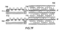
- FIG. 7Fis a schematic illustration of an ion implantation process continued from FIG. 7E .
- a conductive layer 789is formed on top of each formed doped region to complete the fabrication of a test pattern 700 (and also a normal pattern 750 and thus the desired test structure 700 ).
- This stepcan be performed by a silicide (self-aligned silicide) process.
- the right hand side drawingis a top view schematic illustration of the fabricated test structure 700
- the left hand side drawingsare a cross sectional schematic illustration of test pattern 710 along line A-A′ and normal pattern 750 along line B-B′ in the right hand side drawing, respectively.
- doped region 713 and shorter doped region 711are the same conductive type. As a result, electrical conduction is allowed between doped region 713 and the underneath substrate 791 ′ through the shorter doped region 711 , thereby rendering a grounding effect for doped region 713 .
- the shorter doped region 711can thus be seen as a source-to-ground short defect which shorts doped region 713 to the ground (substrate 791 ′).
- test pattern 710has been intentionally made defective by using the modified photolithography masks 7100 and 7200 during ion implantation of p-well and n-well.
- test pattern 710 and normal pattern 750are implemented as an NMOSFET as that described in conjunction with FIG. 2A , wherein well 790 and substrate 791 comprises a p-type dopant, and all doped regions in both test pattern 710 and normal pattern 750 comprise an opposite n-type dopant.
Landscapes
- Engineering & Computer Science (AREA)
- Computer Hardware Design (AREA)
- Microelectronics & Electronic Packaging (AREA)
- General Engineering & Computer Science (AREA)
- Physics & Mathematics (AREA)
- General Physics & Mathematics (AREA)
- Testing Or Measuring Of Semiconductors Or The Like (AREA)
Abstract
Description
Claims (29)
Priority Applications (1)
| Application Number | Priority Date | Filing Date | Title |
|---|---|---|---|
| US12/890,200US8299463B2 (en) | 2009-04-08 | 2010-09-24 | Test structure for charged particle beam inspection and method for defect determination using the same |
Applications Claiming Priority (2)
| Application Number | Priority Date | Filing Date | Title |
|---|---|---|---|
| US12/420,224US8421009B2 (en) | 2009-04-08 | 2009-04-08 | Test structure for charged particle beam inspection and method for defect determination using the same |
| US12/890,200US8299463B2 (en) | 2009-04-08 | 2010-09-24 | Test structure for charged particle beam inspection and method for defect determination using the same |
Related Parent Applications (1)
| Application Number | Title | Priority Date | Filing Date |
|---|---|---|---|
| US12/420,224Continuation-In-PartUS8421009B2 (en) | 2009-04-08 | 2009-04-08 | Test structure for charged particle beam inspection and method for defect determination using the same |
Publications (2)
| Publication Number | Publication Date |
|---|---|
| US20110013826A1 US20110013826A1 (en) | 2011-01-20 |
| US8299463B2true US8299463B2 (en) | 2012-10-30 |
Family
ID=43465344
Family Applications (1)
| Application Number | Title | Priority Date | Filing Date |
|---|---|---|---|
| US12/890,200Expired - Fee RelatedUS8299463B2 (en) | 2009-04-08 | 2010-09-24 | Test structure for charged particle beam inspection and method for defect determination using the same |
Country Status (1)
| Country | Link |
|---|---|
| US (1) | US8299463B2 (en) |
Cited By (16)
| Publication number | Priority date | Publication date | Assignee | Title |
|---|---|---|---|---|
| US8782576B1 (en) | 2013-06-18 | 2014-07-15 | Qualcomm Incorporated | Method and apparatus for a diffusion bridged cell library |
| US9711326B1 (en) | 2016-01-20 | 2017-07-18 | United Microelectronics Corp. | Test structure for electron beam inspection and method for defect determination using electron beam inspection |
| US9711496B1 (en) | 2016-04-04 | 2017-07-18 | Pdf Solutions, Inc. | Integrated circuit containing first and second DOEs of standard cell compatible, NCEM-enabled fill cells, with the first DOE including side-to-side short configured fill cells, and the second DOE including tip-to-side short configured fill cells |
| US9721938B1 (en) | 2016-04-04 | 2017-08-01 | Pdf Solutions, Inc. | Integrated circuit containing first and second DOEs of standard cell compatible, NCEM-enabled fill cells, with the first DOE including tip-to-tip short configured fill cells, and the second DOE including corner short configured fill cells |
| US9748153B1 (en) | 2017-03-29 | 2017-08-29 | Pdf Solutions, Inc. | Process for making and using a semiconductor wafer containing first and second does of standard cell compatible, NCEM-enabled fill cells, with the first DOE including side-to-side short configured fill cells, and the second DOE including tip-to-side short configure |
| US9768083B1 (en) | 2017-06-27 | 2017-09-19 | Pdf Solutions, Inc. | Process for making and using a semiconductor wafer containing first and second DOEs of standard cell compatible, NCEM-enabled fill cells, with the first DOE including merged-via open configured fill cells, and the second DOE including snake open configured fill cells |
| US9773774B1 (en) | 2017-03-30 | 2017-09-26 | Pdf Solutions, Inc. | Process for making and using a semiconductor wafer containing first and second DOEs of standard cell compatible, NCEM-enabled fill cells, with the first DOE including chamfer short configured fill cells, and the second DOE including corner short configured fill cells |
| US9786649B1 (en) | 2017-06-27 | 2017-10-10 | Pdf Solutions, Inc. | Process for making and using a semiconductor wafer containing first and second DOEs of standard cell compatible, NCEM-enabled fill cells, with the first DOE including via open configured fill cells, and the second DOE including stitch open configured fill cells |
| US9865583B1 (en) | 2017-06-28 | 2018-01-09 | Pdf Solutions, Inc. | Process for making and using a semiconductor wafer containing first and second DOEs of standard cell compatible, NCEM-enabled fill cells, with the first DOE including snake open configured fill cells, and the second DOE including stitch open configured fill cells |
| US9929063B1 (en) | 2016-04-04 | 2018-03-27 | Pdf Solutions, Inc. | Process for making an integrated circuit that includes NCEM-Enabled, tip-to-side gap-configured fill cells, with NCEM pads formed from at least three conductive stripes positioned between adjacent gates |
| US9984944B1 (en) | 2015-12-16 | 2018-05-29 | Pdf Solutions, Inc. | Integrated circuit containing DOEs of GATECNT-tip-to-side-short-configured, NCEM-enabled fill cells |
| US10096530B1 (en) | 2017-06-28 | 2018-10-09 | Pdf Solutions, Inc. | Process for making and using a semiconductor wafer containing first and second DOEs of standard cell compatible, NCEM-enabled fill cells, with the first DOE including merged-via open configured fill cells, and the second DOE including stitch open configured fill cells |
| US10199287B1 (en) | 2015-02-03 | 2019-02-05 | Pdf Solutions, Inc. | Method for processing a semiconductor wafer using non-contact electrical measurements indicative of at least one tip-to-side short or leakage, at least one chamfer short or leakage, and at least one via open or resistance, where such measurements are obtained from non-contact pads associated with respective tip-to-side short, chamfer short, and via open test areas |
| US10593604B1 (en) | 2015-12-16 | 2020-03-17 | Pdf Solutions, Inc. | Process for making semiconductor dies, chips, and wafers using in-line measurements obtained from DOEs of NCEM-enabled fill cells |
| US10978438B1 (en) | 2015-12-16 | 2021-04-13 | Pdf Solutions, Inc. | IC with test structures and E-beam pads embedded within a contiguous standard cell area |
| US11125804B2 (en)* | 2018-12-12 | 2021-09-21 | Shanghai Huali Integrated Circuit Mfg. Co. Ltd. | Failure positioning method |
Families Citing this family (10)
| Publication number | Priority date | Publication date | Assignee | Title |
|---|---|---|---|---|
| US8787074B2 (en) | 2011-10-14 | 2014-07-22 | International Business Machines Corporation | Static random access memory test structure |
| US9291665B2 (en) | 2012-05-14 | 2016-03-22 | Globalfoundries Inc. | Evaluating transistors with e-beam inspection |
| US9805994B1 (en) | 2015-02-03 | 2017-10-31 | Pdf Solutions, Inc. | Mesh-style NCEM pads, and process for making semiconductor dies, chips, and wafers using in-line measurements from such pads |
| US10234500B2 (en)* | 2015-04-17 | 2019-03-19 | Globalfoundries Inc. | Systematic defects inspection method with combined eBeam inspection and net tracing classification |
| KR101774267B1 (en)* | 2016-06-27 | 2017-09-04 | 주식회사 한글과컴퓨터 | Collaborative support apparatus for collaborative editing of electronic documents and operating method thereof |
| US10818595B2 (en) | 2016-11-29 | 2020-10-27 | Taiwan Semiconductor Manufacturing Co., Ltd. | Semiconductor structure, testing and fabricating methods thereof |
| WO2021068219A1 (en)* | 2019-10-12 | 2021-04-15 | Yangtze Memory Technologies Co., Ltd. | Method for detecting defects in deep features with laser enhanced electron tunneling effect |
| CN118974574A (en)* | 2022-04-05 | 2024-11-15 | 应用材料公司 | Method and apparatus for testing a package substrate |
| US12061229B2 (en)* | 2022-06-28 | 2024-08-13 | Taiwan Semiconductor Manufacturing Company, Ltd. | In-line electrical detection of defects at wafer level |
| CN118398603B (en)* | 2024-06-25 | 2024-08-23 | 杭州积海半导体有限公司 | Test structure of MOS transistor |
Citations (10)
| Publication number | Priority date | Publication date | Assignee | Title |
|---|---|---|---|---|
| US5976925A (en)* | 1997-12-01 | 1999-11-02 | Advanced Micro Devices | Process of fabricating a semiconductor devise having asymmetrically-doped active region and gate electrode |
| US6069045A (en)* | 1996-05-31 | 2000-05-30 | Nec Corporation | Method of forming C49-structure tungsten-containing titanium salicide structure |
| US6242776B1 (en)* | 1999-06-02 | 2001-06-05 | Advanced Micro Devices, Inc. | Device improvement by lowering LDD resistance with new silicide process |
| US6452412B1 (en)* | 1999-03-04 | 2002-09-17 | Advanced Micro Devices, Inc. | Drop-in test structure and methodology for characterizing an integrated circuit process flow and topography |
| US20070221990A1 (en)* | 2006-03-22 | 2007-09-27 | International Business Machines Corporation | Grounding front-end-of-line structures on a soi substrate |
| US20070222470A1 (en)* | 2006-03-22 | 2007-09-27 | International Business Machines Corporation | Buried short location determination using voltage contrast inspection |
| US20080237586A1 (en)* | 2007-03-30 | 2008-10-02 | Min Chul Sun | Semiconductor Integrated Test Structures For Electron Beam Inspection of Semiconductor Wafers |
| US20080267489A1 (en) | 2007-04-24 | 2008-10-30 | Hermes- Microvision, Inc. | Method for determining abnormal characteristics in integrated circuit manufacturing process |
| US20100055809A1 (en)* | 2008-09-02 | 2010-03-04 | Spansion Llc | Process of fabricating a workpiece using a test mask |
| US8089297B2 (en)* | 2007-04-25 | 2012-01-03 | Hermes-Microvision, Inc. | Structure and method for determining a defect in integrated circuit manufacturing process |
- 2010
- 2010-09-24USUS12/890,200patent/US8299463B2/ennot_activeExpired - Fee Related
Patent Citations (16)
| Publication number | Priority date | Publication date | Assignee | Title |
|---|---|---|---|---|
| US6069045A (en)* | 1996-05-31 | 2000-05-30 | Nec Corporation | Method of forming C49-structure tungsten-containing titanium salicide structure |
| US6114765A (en)* | 1996-05-31 | 2000-09-05 | Nec Corporation | C49-structured tungsten-containing titanium salicide structure and method of forming the same |
| US5976925A (en)* | 1997-12-01 | 1999-11-02 | Advanced Micro Devices | Process of fabricating a semiconductor devise having asymmetrically-doped active region and gate electrode |
| US6452412B1 (en)* | 1999-03-04 | 2002-09-17 | Advanced Micro Devices, Inc. | Drop-in test structure and methodology for characterizing an integrated circuit process flow and topography |
| US6242776B1 (en)* | 1999-06-02 | 2001-06-05 | Advanced Micro Devices, Inc. | Device improvement by lowering LDD resistance with new silicide process |
| US20070222470A1 (en)* | 2006-03-22 | 2007-09-27 | International Business Machines Corporation | Buried short location determination using voltage contrast inspection |
| US20070221990A1 (en)* | 2006-03-22 | 2007-09-27 | International Business Machines Corporation | Grounding front-end-of-line structures on a soi substrate |
| US7474107B2 (en)* | 2006-03-22 | 2009-01-06 | International Business Machines Corporation | Buried short location determination using voltage contrast inspection |
| US7518190B2 (en)* | 2006-03-22 | 2009-04-14 | International Business Machines Corporation | Grounding front-end-of-line structures on a SOI substrate |
| US20090146211A1 (en)* | 2006-03-22 | 2009-06-11 | Cote William J | Grounding front-end-of-line structures on a soi substrate |
| US7732866B2 (en)* | 2006-03-22 | 2010-06-08 | International Business Machines Corporation | Grounding front-end-of-line structures on a SOI substrate |
| US7679083B2 (en)* | 2007-03-30 | 2010-03-16 | Samsung Electronics Co., Ltd. | Semiconductor integrated test structures for electron beam inspection of semiconductor wafers |
| US20080237586A1 (en)* | 2007-03-30 | 2008-10-02 | Min Chul Sun | Semiconductor Integrated Test Structures For Electron Beam Inspection of Semiconductor Wafers |
| US20080267489A1 (en) | 2007-04-24 | 2008-10-30 | Hermes- Microvision, Inc. | Method for determining abnormal characteristics in integrated circuit manufacturing process |
| US8089297B2 (en)* | 2007-04-25 | 2012-01-03 | Hermes-Microvision, Inc. | Structure and method for determining a defect in integrated circuit manufacturing process |
| US20100055809A1 (en)* | 2008-09-02 | 2010-03-04 | Spansion Llc | Process of fabricating a workpiece using a test mask |
Cited By (62)
| Publication number | Priority date | Publication date | Assignee | Title |
|---|---|---|---|---|
| US8782576B1 (en) | 2013-06-18 | 2014-07-15 | Qualcomm Incorporated | Method and apparatus for a diffusion bridged cell library |
| US9070551B2 (en)* | 2013-06-18 | 2015-06-30 | Qualcomm Incorporated | Method and apparatus for a diffusion bridged cell library |
| US10199283B1 (en) | 2015-02-03 | 2019-02-05 | Pdf Solutions, Inc. | Method for processing a semiconductor wager using non-contact electrical measurements indicative of a resistance through a stitch, where such measurements are obtained by scanning a pad comprised of at least three parallel conductive stripes using a moving stage with beam deflection to account for motion of the stage |
| US10211111B1 (en) | 2015-02-03 | 2019-02-19 | Pdf Solutions, Inc. | Method for processing a semiconductor wafer using non-contact electrical measurements indicative of at least one tip-to-tip short or leakage, at least one tip-to-side short or leakage, and at least one corner short or leakage, where such measurements are obtained from non-contact pads associated with respective tip-to-tip short, tip-to-side sort, and corner short test areas |
| US10199287B1 (en) | 2015-02-03 | 2019-02-05 | Pdf Solutions, Inc. | Method for processing a semiconductor wafer using non-contact electrical measurements indicative of at least one tip-to-side short or leakage, at least one chamfer short or leakage, and at least one via open or resistance, where such measurements are obtained from non-contact pads associated with respective tip-to-side short, chamfer short, and via open test areas |
| US10199288B1 (en) | 2015-02-03 | 2019-02-05 | Pdf Solutions, Inc. | Method for processing a semiconductor wafer using non-contact electrical measurements indicative of at least one side-to-side short or leakage, at least one corner short or leakage, and at least one via open or resistance, where such measurements are obtained from non-contact pads associated with respective side-to-side short, corner short, and via open test areas |
| US10199286B1 (en) | 2015-02-03 | 2019-02-05 | Pdf Solutions, Inc. | Method for processing a semiconductor wafer using non-contact electrical measurements indicative of at least one tip-to-side short or leakage, at least one chamfer short or leakage, and at least one corner short or leakage, where such measurements are obtained from non-contact pads associated with respective tip-to-side short, chamfer short, and corner short test areas |
| US10199289B1 (en) | 2015-02-03 | 2019-02-05 | Pdf Solutions, Inc. | Method for processing a semiconductor wafer using non-contact electrical measurements indicative of at least one chamfer short or leakage, at least one corner short or leakage, and at least one via open or resistance, where such measurements are obtained from non-contact pads associated with respective chamfer short, corner short, and via open test areas |
| US10211112B1 (en) | 2015-02-03 | 2019-02-19 | Pdf Solutions, Inc. | Method for processing a semiconductor wafer using non-contact electrical measurements indicative of at least one tip-to-tip short or leakage, at least one tip-to-side short or leakage, and at least one side-to-side short or leakage, where such measurements are obtained from non-contact pads associated with respective tip-to-tip short, tip-to-side short, and side-to-side short test areas |
| US10854522B1 (en) | 2015-02-03 | 2020-12-01 | Pdf Solutions, Inc. | Method for processing a semiconductor wafer using non-contact electrical measurements indicative of at least one tip-to-side short or leakage, at least one corner short or leakage, and at least one via open or resistance, where such measurements are obtained from non-contact pads associated with respective tip-to-side short, corner short, and via open test areas |
| US10777472B1 (en) | 2015-02-03 | 2020-09-15 | Pdf Solutions, Inc. | IC with test structures embedded within a contiguous standard cell area |
| US10199294B1 (en) | 2015-02-03 | 2019-02-05 | Pdf Solutions, Inc. | Method for processing a semiconductor wafer using non-contact electrical measurements indicative of a least one side-to-side short or leakage, at least one via-chamfer short or leakage, and at least one corner short or leakage, where such measurements are obtained from cells with respective side-to-side short, via-chamfer short, and corner short test areas, using a charged particle-beam inspector with beam deflection to account for motion of the stage |
| US10199290B1 (en) | 2015-02-03 | 2019-02-05 | Pdf Solutions, Inc. | Method for processing a semiconductor wafer using non-contact electrical measurements indicative of at least one tip-to-tip short or leakage, at least one tip-to-side short or leakage, and at least one side-to-side short or leakage, where such measurements are obtained from cells with respective tip-to-tip short, tip-to-side short, and side-to-side short test areas, using a charged particle-beam inspector with beam deflection to account for motion of the stage |
| US10199285B1 (en) | 2015-02-03 | 2019-02-05 | Pdf Solutions, Inc. | Method for processing a semiconductor wafer using non-contact electrical measurements indicative of at least one tip-to-tip short or leakage, at least one side-to-side short or leakages, and at least one via respective tip-to-tip short, side-to-side short, and via open test areas |
| US10290552B1 (en) | 2015-02-03 | 2019-05-14 | Pdf Solutions, Inc. | Methods for processing a semiconductor wafer using non-contact electrical measurements indicative of at least one tip-to-tip short or leakage, at least one via-chamfer short or leakage, and at least one corner short or leakage, where such measurements are obtained from cells with respective tip-to-tip short, via-chamfer short, and corner short test areas, using a charged particle-beam inspector with beam deflection to account for motion of the stage |
| US10199284B1 (en) | 2015-02-03 | 2019-02-05 | Pdf Solutions, Inc. | Method for processing a semiconductor wafer using non-contact electrical measurements indicative of at least one tip-to-tip short or leakage, at least one tip-to-side short or leakage, and at least one chamfer short or leakage, where such measurements are obtained from non-contact pads associated with respective tip-to-tip short, tip-to-side short, and chamfer short test areas |
| US10199293B1 (en) | 2015-02-03 | 2019-02-05 | Pdf Solutions, Inc. | Method for processing a semiconductor water using non-contact electrical measurements indicative of at least one tip-to-tip short or leakage, at least one side-to-side short or leakage, and at least one chamfer short or leakage, where such measurements are obtained from non-contact pads associated with respective tip-to-tip short, side to side short, and chamfer short test areas |
| US9984944B1 (en) | 2015-12-16 | 2018-05-29 | Pdf Solutions, Inc. | Integrated circuit containing DOEs of GATECNT-tip-to-side-short-configured, NCEM-enabled fill cells |
| US10978438B1 (en) | 2015-12-16 | 2021-04-13 | Pdf Solutions, Inc. | IC with test structures and E-beam pads embedded within a contiguous standard cell area |
| US11107804B1 (en) | 2015-12-16 | 2021-08-31 | Pdf Solutions, Inc. | IC with test structures and e-beam pads embedded within a contiguous standard cell area |
| US10593604B1 (en) | 2015-12-16 | 2020-03-17 | Pdf Solutions, Inc. | Process for making semiconductor dies, chips, and wafers using in-line measurements obtained from DOEs of NCEM-enabled fill cells |
| US11018126B1 (en) | 2015-12-16 | 2021-05-25 | Pdf Solutions, Inc. | IC with test structures and e-beam pads embedded within a contiguous standard cell area |
| US11075194B1 (en) | 2015-12-16 | 2021-07-27 | Pdf Solutions, Inc. | IC with test structures and E-beam pads embedded within a contiguous standard cell area |
| US11081476B1 (en) | 2015-12-16 | 2021-08-03 | Pdf Solutions, Inc. | IC with test structures and e-beam pads embedded within a contiguous standard cell area |
| US11081477B1 (en) | 2015-12-16 | 2021-08-03 | Pdf Solutions, Inc. | IC with test structures and e-beam pads embedded within a contiguous standard cell area |
| US9711326B1 (en) | 2016-01-20 | 2017-07-18 | United Microelectronics Corp. | Test structure for electron beam inspection and method for defect determination using electron beam inspection |
| US9786650B1 (en) | 2016-04-04 | 2017-10-10 | Pdf Solutions, Inc. | Process for making and using a semiconductor wafer containing first and second DOEs of standard cell compatible, NCEM-enabled fill cells, with the first DOE including snake open configured fill cells, and the second DOE including metal island open configured fill cells |
| US9825018B1 (en) | 2016-04-04 | 2017-11-21 | Pdf Solutions, Inc. | Integrated circuit containing first and second DOEs of standard cell compatible, NCEM-enabled fill cells, with the first DOE including tip-to-tip short configured fill cells, and the second DOE including chamfer short configured fill cells |
| US9911670B1 (en) | 2016-04-04 | 2018-03-06 | Pdf Solutions, Inc. | Integrated circuit including NCEM-enabled, via-open/resistance-configured fill cells, with NCEM pads formed from at least three conductive stripes positioned between adjacent gate |
| US9922890B1 (en) | 2016-04-04 | 2018-03-20 | Pdf Solutions, Inc. | Integrated circuit including NCEM-enabled, snake-configured fill cells, with NCEM pads formed from at least three conductive stripes positioned between adjacent gates |
| US9922968B1 (en) | 2016-04-04 | 2018-03-20 | Pdf Solutions, Inc. | Process for making and using a semiconductor wafer containing first and second DOEs of standard cell compatible, NCEM-enabled fill cells, with the first DOE including side-to-side short configured fill cells, and the second DOE including chamfer short configured fill cells |
| US9929136B1 (en) | 2016-04-04 | 2018-03-27 | Pdf Solutions, Inc. | Process for making and using a semiconductor wafer containing first and second DOEs of standard cell compatible, NCEM-Enabled fill cells, with the first DOE including tip-to-side short configured fill cells, and the second DOE including chamfer short configured fill cells |
| US9929063B1 (en) | 2016-04-04 | 2018-03-27 | Pdf Solutions, Inc. | Process for making an integrated circuit that includes NCEM-Enabled, tip-to-side gap-configured fill cells, with NCEM pads formed from at least three conductive stripes positioned between adjacent gates |
| US9947601B1 (en) | 2016-04-04 | 2018-04-17 | Pdf Solutions, Inc. | Integrated circuit including NCEM-enabled, side-to-side gap-configured fill cells, with NCEM pads formed from at least three conductive stripes positioned between adjacent gates |
| US9911669B1 (en) | 2016-04-04 | 2018-03-06 | Pdf Solutions, Inc. | Integrated circuit including NCEM-enabled, diagonal gap-configured fill cells, with NCEM pads formed from at least three conductive stripes positioned between adjacent gates |
| US10096529B1 (en) | 2016-04-04 | 2018-10-09 | Pdf Solutions, Inc. | Process for making and using a semiconductor wafer containing first and second DOEs of standard cell compatible, NCEM-enabled fill cells, with the first DOE including via open configured fill cells, and the second DOE including metal island open configured fill cells |
| US9711496B1 (en) | 2016-04-04 | 2017-07-18 | Pdf Solutions, Inc. | Integrated circuit containing first and second DOEs of standard cell compatible, NCEM-enabled fill cells, with the first DOE including side-to-side short configured fill cells, and the second DOE including tip-to-side short configured fill cells |
| US10109539B1 (en) | 2016-04-04 | 2018-10-23 | Pdf Solutions, Inc. | Integrated circuit including NCEM-enabled, tip-to-side gap-configured fill cells, with NCEM pads formed from at least three conductive stripes positioned between adjacent gates |
| US9899276B1 (en) | 2016-04-04 | 2018-02-20 | Pdf Solutions, Inc. | Process for making an integrated circuit that includes NCEM-enabled, interlayer overlap-configured fill cells, with NCEM pads formed from at least three conductive stripes positioned between adjacent gates |
| US9881843B1 (en) | 2016-04-04 | 2018-01-30 | Pdf Solutions, Inc. | Integrated circuit including NCEM-Enabled, tip-to-tip gap-configured fill cells, with NCEM pads formed from at least three conductive stripes positioned between adjacent gates |
| US9870962B1 (en) | 2016-04-04 | 2018-01-16 | Pdf Solutions, Inc. | Integrated circuit including NCEM-enabled, interlayer overlap-configured fill cells, with NCEM pads formed from at least three conductive stripes positioned between adjacent gates |
| US9871028B1 (en) | 2016-04-04 | 2018-01-16 | Pdf Solutions, Inc. | Process for making and using a semiconductor wafer containing first and second DOEs of standard cell compatible, NCEM-enabled fill cells, with the first DOE including tip-to-tip short configured fill cells, and the second DOE including chamfer short configured fill cells |
| US9721938B1 (en) | 2016-04-04 | 2017-08-01 | Pdf Solutions, Inc. | Integrated circuit containing first and second DOEs of standard cell compatible, NCEM-enabled fill cells, with the first DOE including tip-to-tip short configured fill cells, and the second DOE including corner short configured fill cells |
| US9911668B1 (en) | 2016-04-04 | 2018-03-06 | Pdf Solutions, Inc. | Integrated circuit including NCEM-enabled, corner gap-configured fill cells, with NCEM pads formed from at least three conductive stripes positioned between adjacent gates |
| US9818660B1 (en) | 2016-04-04 | 2017-11-14 | Pdf Solutions, Inc. | Integrated circuit containing first and second DOEs of standard cell compatible, NCEM-enabled fill cells, with the first DOE including via open configured fill cells, and the second DOE including metal island open configured fill cells |
| US9818738B1 (en) | 2016-04-04 | 2017-11-14 | Pdf Solutions, Inc. | Integrated circuit containing first and second DOEs of standard cell compatible, NCEM-enabled fill cells with first DOE including tip-to-side short configured fill cells and second DOE including chamfer short configured fill cells |
| US9799640B1 (en) | 2016-04-04 | 2017-10-24 | Pdf Solutions, Inc. | Integrated circuit containing first and second DOEs of standard cell compatible, NCEM-enabled fill cells, with the first DOE including chamfer short configured fill cells, and the second DOE including corner short configured fill cells |
| US9721937B1 (en) | 2016-04-04 | 2017-08-01 | Pdf Solutions, Inc. | Integrated circuit containing first and second does of standard cell compatible, NCEM-enabled fill cells, with the first DOE including side-to-side short configured fill cells, and the second DOE including tip-to-tip short configured fill cells |
| US9785496B1 (en) | 2016-04-04 | 2017-10-10 | Pdf Solutions, Inc. | Process for making semiconductor dies, chips, and wafers using non-contact measurements obtained from DOEs of NCEM-enabled fill cells on wafers that include multiple steps for enabling NC detecteion of AACNT-TS via opens |
| US9778974B1 (en) | 2016-04-04 | 2017-10-03 | Pdf Solutions, Inc. | Integrated circuit containing first and second DOEs of standard cell compatible, NCEM-enabled fill cells, with the first DOE including snake open configured fill cells, and the second DOE including metal island open configured fill cells |
| US10269786B1 (en) | 2016-04-04 | 2019-04-23 | Pdf Solutions, Inc. | Integrated circuit containing first and second DOEs of standard Cell Compatible, NCEM-enabled Fill Cells, with the first DOE including tip-to-side short configured fill cells, and the second DOE including corner short configured fill cells |
| US9761502B1 (en) | 2016-04-04 | 2017-09-12 | Pdf Solutions, Inc. | Integrated circuit containing first and second DOEs of standard cell compatible, NCEM-enabled fill cells, with the first DOE including via open configured fill cells, and the second DOE including merged-via configured fill cells |
| US9773775B1 (en) | 2016-04-04 | 2017-09-26 | Pdf Solutions, Inc. | Integrated circuit containing first and second DOEs of standard cell compatible, NCEM-enabled fill cells, with the first DOE including merged-via open configured fill cells, and the second DOE including snake open configured fill cells |
| US9766970B1 (en) | 2016-04-04 | 2017-09-19 | Pdf Solutions, Inc. | Integrated circuit containing first and second DOEs of standard cell compatible, NCEM-enabled fill cells, with the first DOE including merged-via open configured fill cells, and the second DOE including metal island open configured fill cells |
| US9768156B1 (en) | 2016-04-04 | 2017-09-19 | Pdf Solutions, Inc. | Integrated circuit containing first and second DOEs of standard cell compatible, NCEM-enabled fill cells, with the first DOE including side-to-side short configured fill cells, and the second DOE including chamfer short configured fill cells |
| US9748153B1 (en) | 2017-03-29 | 2017-08-29 | Pdf Solutions, Inc. | Process for making and using a semiconductor wafer containing first and second does of standard cell compatible, NCEM-enabled fill cells, with the first DOE including side-to-side short configured fill cells, and the second DOE including tip-to-side short configure |
| US9773774B1 (en) | 2017-03-30 | 2017-09-26 | Pdf Solutions, Inc. | Process for making and using a semiconductor wafer containing first and second DOEs of standard cell compatible, NCEM-enabled fill cells, with the first DOE including chamfer short configured fill cells, and the second DOE including corner short configured fill cells |
| US9768083B1 (en) | 2017-06-27 | 2017-09-19 | Pdf Solutions, Inc. | Process for making and using a semiconductor wafer containing first and second DOEs of standard cell compatible, NCEM-enabled fill cells, with the first DOE including merged-via open configured fill cells, and the second DOE including snake open configured fill cells |
| US9786649B1 (en) | 2017-06-27 | 2017-10-10 | Pdf Solutions, Inc. | Process for making and using a semiconductor wafer containing first and second DOEs of standard cell compatible, NCEM-enabled fill cells, with the first DOE including via open configured fill cells, and the second DOE including stitch open configured fill cells |
| US9865583B1 (en) | 2017-06-28 | 2018-01-09 | Pdf Solutions, Inc. | Process for making and using a semiconductor wafer containing first and second DOEs of standard cell compatible, NCEM-enabled fill cells, with the first DOE including snake open configured fill cells, and the second DOE including stitch open configured fill cells |
| US10096530B1 (en) | 2017-06-28 | 2018-10-09 | Pdf Solutions, Inc. | Process for making and using a semiconductor wafer containing first and second DOEs of standard cell compatible, NCEM-enabled fill cells, with the first DOE including merged-via open configured fill cells, and the second DOE including stitch open configured fill cells |
| US11125804B2 (en)* | 2018-12-12 | 2021-09-21 | Shanghai Huali Integrated Circuit Mfg. Co. Ltd. | Failure positioning method |
Also Published As
| Publication number | Publication date |
|---|---|
| US20110013826A1 (en) | 2011-01-20 |
Similar Documents
| Publication | Publication Date | Title |
|---|---|---|
| US8299463B2 (en) | Test structure for charged particle beam inspection and method for defect determination using the same | |
| US8421009B2 (en) | Test structure for charged particle beam inspection and method for defect determination using the same | |
| US7772866B2 (en) | Structure and method of mapping signal intensity to surface voltage for integrated circuit inspection | |
| US8089297B2 (en) | Structure and method for determining a defect in integrated circuit manufacturing process | |
| US8294485B2 (en) | Detecting asymmetrical transistor leakage defects | |
| US6630724B1 (en) | Gate dielectric antifuse circuits and methods for operating same | |
| Patterson et al. | Test structure and e-beam inspection methodology for in-line detection of (non-visual) missing spacer defects | |
| US5646438A (en) | Programmable semiconductor memory | |
| US20080267489A1 (en) | Method for determining abnormal characteristics in integrated circuit manufacturing process | |
| US20080153225A1 (en) | Non-Volatile Memory In CMOS Logic Process | |
| KR19990013871A (en) | Method and apparatus for testing the structure of semiconductors and integrated circuits | |
| US7859285B2 (en) | Device under test array for identifying defects | |
| US20020176972A1 (en) | Contact chain for testing and its relevantly debugging method | |
| US6995027B2 (en) | Integrated semiconductor structure for reliability tests of dielectrics | |
| CN118198037B (en) | Test structure and test method for polycrystalline silicon defects | |
| US20150123130A1 (en) | Test key structure | |
| US20240202305A1 (en) | Two-transistor chip and three-transistor chip identification bit cells | |
| KR20050088186A (en) | Method of producing semiconductor elements using a test structure | |
| CN114783500A (en) | Electrical test method and test structure of semiconductor device | |
| KR101585972B1 (en) | Semiconductor memory device of single gate structure and semiconductor memory device array of single gate structure | |
| KR101598075B1 (en) | A semiconductor memory element having a single gate structure and a semiconductor memory element array having a single gate structure | |
| CN107293503A (en) | Test structure, preparation method and the method for testing of shared contact hole circuit defect | |
| US7495254B2 (en) | Test structure and method for detecting and studying crystal lattice dislocation defects in integrated circuit devices | |
| US9685387B1 (en) | Test key for checking the window of a doped region and method of using the test key | |
| CN120468616B (en) | Test structure and test method for semiconductor device |
Legal Events
| Date | Code | Title | Description |
|---|---|---|---|
| AS | Assignment | Owner name:HERMES MICROVISION, INC., TAIWAN Free format text:ASSIGNMENT OF ASSIGNORS INTEREST;ASSIGNOR:XIAO, HONG;REEL/FRAME:025045/0659 Effective date:20100917 | |
| ZAAA | Notice of allowance and fees due | Free format text:ORIGINAL CODE: NOA | |
| ZAAB | Notice of allowance mailed | Free format text:ORIGINAL CODE: MN/=. | |
| STCF | Information on status: patent grant | Free format text:PATENTED CASE | |
| FPAY | Fee payment | Year of fee payment:4 | |
| FEPP | Fee payment procedure | Free format text:PAYOR NUMBER ASSIGNED (ORIGINAL EVENT CODE: ASPN); ENTITY STATUS OF PATENT OWNER: LARGE ENTITY | |
| MAFP | Maintenance fee payment | Free format text:PAYMENT OF MAINTENANCE FEE, 8TH YEAR, LARGE ENTITY (ORIGINAL EVENT CODE: M1552); ENTITY STATUS OF PATENT OWNER: LARGE ENTITY Year of fee payment:8 | |
| AS | Assignment | Owner name:HERMES MICROVISION INCORPORATED B.V., NETHERLANDS Free format text:ASSIGNMENT OF ASSIGNORS INTEREST;ASSIGNOR:HERMES MICROVISION, INC.;REEL/FRAME:054866/0742 Effective date:20181219 Owner name:ASML NETHERLANDS B.V., NETHERLANDS Free format text:ASSIGNMENT OF ASSIGNORS INTEREST;ASSIGNOR:HERMES MICROVISION INCORPORATED B.V.;REEL/FRAME:054870/0156 Effective date:20181219 | |
| FEPP | Fee payment procedure | Free format text:MAINTENANCE FEE REMINDER MAILED (ORIGINAL EVENT CODE: REM.); ENTITY STATUS OF PATENT OWNER: LARGE ENTITY | |
| LAPS | Lapse for failure to pay maintenance fees | Free format text:PATENT EXPIRED FOR FAILURE TO PAY MAINTENANCE FEES (ORIGINAL EVENT CODE: EXP.); ENTITY STATUS OF PATENT OWNER: LARGE ENTITY | |
| STCH | Information on status: patent discontinuation | Free format text:PATENT EXPIRED DUE TO NONPAYMENT OF MAINTENANCE FEES UNDER 37 CFR 1.362 | |
| FP | Lapsed due to failure to pay maintenance fee | Effective date:20241030 |