US8298925B2 - Mechanisms for forming ultra shallow junction - Google Patents
Mechanisms for forming ultra shallow junctionDownload PDFInfo
- Publication number
- US8298925B2 US8298925B2US12/941,509US94150910AUS8298925B2US 8298925 B2US8298925 B2US 8298925B2US 94150910 AUS94150910 AUS 94150910AUS 8298925 B2US8298925 B2US 8298925B2
- Authority
- US
- United States
- Prior art keywords
- doping
- plasma
- dopant
- fin structures
- shallow
- Prior art date
- Legal status (The legal status is an assumption and is not a legal conclusion. Google has not performed a legal analysis and makes no representation as to the accuracy of the status listed.)
- Active, expires
Links
- 230000007246mechanismEffects0.000titledescription2
- 238000000034methodMethods0.000claimsabstractdescription150
- 230000008569processEffects0.000claimsabstractdescription99
- 239000002019doping agentSubstances0.000claimsabstractdescription73
- 239000012159carrier gasSubstances0.000claimsabstractdescription37
- 239000000758substrateSubstances0.000claimsdescription67
- 239000007789gasSubstances0.000claimsdescription46
- ZOXJGFHDIHLPTG-UHFFFAOYSA-NBoronChemical group[B]ZOXJGFHDIHLPTG-UHFFFAOYSA-N0.000claimsdescription11
- 229910052796boronInorganic materials0.000claimsdescription11
- 238000000137annealingMethods0.000claimsdescription10
- 230000005669field effectEffects0.000claimsdescription7
- 229910052786argonInorganic materials0.000claimsdescription4
- 229910052743kryptonInorganic materials0.000claimsdescription4
- 229910052754neonInorganic materials0.000claimsdescription4
- 229910052724xenonInorganic materials0.000claimsdescription3
- 229910052785arsenicInorganic materials0.000claimsdescription2
- BHEPBYXIRTUNPN-UHFFFAOYSA-Nhydridophosphorus(.) (triplet)Chemical compound[PH]BHEPBYXIRTUNPN-UHFFFAOYSA-N0.000claimsdescription2
- 210000002381plasmaAnatomy0.000claims27
- RQNWIZPPADIBDY-UHFFFAOYSA-Narsenic atomChemical compound[As]RQNWIZPPADIBDY-UHFFFAOYSA-N0.000claims1
- 230000015572biosynthetic processEffects0.000abstractdescription3
- 239000004065semiconductorSubstances0.000description20
- 150000002500ionsChemical class0.000description14
- 238000010884ion-beam techniqueMethods0.000description9
- 238000004519manufacturing processMethods0.000description9
- 239000000203mixtureSubstances0.000description6
- 230000006870functionEffects0.000description5
- 239000000463materialSubstances0.000description5
- 238000004151rapid thermal annealingMethods0.000description5
- 238000005468ion implantationMethods0.000description4
- 238000004377microelectronicMethods0.000description4
- 230000037230mobilityEffects0.000description4
- 238000011982device technologyMethods0.000description3
- 238000002513implantationMethods0.000description3
- 238000002955isolationMethods0.000description3
- XUIMIQQOPSSXEZ-UHFFFAOYSA-NSiliconChemical compound[Si]XUIMIQQOPSSXEZ-UHFFFAOYSA-N0.000description2
- 238000009792diffusion processMethods0.000description2
- 238000010790dilutionMethods0.000description2
- 239000012895dilutionSubstances0.000description2
- 238000005516engineering processMethods0.000description2
- 229910052732germaniumInorganic materials0.000description2
- GNPVGFCGXDBREM-UHFFFAOYSA-Ngermanium atomChemical compound[Ge]GNPVGFCGXDBREM-UHFFFAOYSA-N0.000description2
- 238000012986modificationMethods0.000description2
- 230000004048modificationEffects0.000description2
- 238000012545processingMethods0.000description2
- 239000000376reactantSubstances0.000description2
- 238000001004secondary ion mass spectrometryMethods0.000description2
- 229910052710siliconInorganic materials0.000description2
- 239000010703siliconSubstances0.000description2
- 229910000577Silicon-germaniumInorganic materials0.000description1
- 230000005856abnormalityEffects0.000description1
- 238000009825accumulationMethods0.000description1
- 230000005540biological transmissionEffects0.000description1
- -1boron (B) ionsChemical class0.000description1
- 239000004020conductorSubstances0.000description1
- 238000010586diagramMethods0.000description1
- 229910003460diamondInorganic materials0.000description1
- 239000010432diamondSubstances0.000description1
- 239000003989dielectric materialSubstances0.000description1
- 238000007865dilutingMethods0.000description1
- 230000009977dual effectEffects0.000description1
- 230000000694effectsEffects0.000description1
- 229910052734heliumInorganic materials0.000description1
- 230000006872improvementEffects0.000description1
- 239000012535impuritySubstances0.000description1
- 239000011261inert gasSubstances0.000description1
- 238000005259measurementMethods0.000description1
- 239000011800void materialSubstances0.000description1
Images


Classifications
- H—ELECTRICITY
- H10—SEMICONDUCTOR DEVICES; ELECTRIC SOLID-STATE DEVICES NOT OTHERWISE PROVIDED FOR
- H10D—INORGANIC ELECTRIC SEMICONDUCTOR DEVICES
- H10D30/00—Field-effect transistors [FET]
- H10D30/60—Insulated-gate field-effect transistors [IGFET]
- H10D30/611—Insulated-gate field-effect transistors [IGFET] having multiple independently-addressable gate electrodes influencing the same channel
- H—ELECTRICITY
- H01—ELECTRIC ELEMENTS
- H01L—SEMICONDUCTOR DEVICES NOT COVERED BY CLASS H10
- H01L21/00—Processes or apparatus adapted for the manufacture or treatment of semiconductor or solid state devices or of parts thereof
- H01L21/02—Manufacture or treatment of semiconductor devices or of parts thereof
- H01L21/04—Manufacture or treatment of semiconductor devices or of parts thereof the devices having potential barriers, e.g. a PN junction, depletion layer or carrier concentration layer
- H01L21/18—Manufacture or treatment of semiconductor devices or of parts thereof the devices having potential barriers, e.g. a PN junction, depletion layer or carrier concentration layer the devices having semiconductor bodies comprising elements of Group IV of the Periodic Table or AIIIBV compounds with or without impurities, e.g. doping materials
- H01L21/22—Diffusion of impurity materials, e.g. doping materials, electrode materials, into or out of a semiconductor body, or between semiconductor regions; Interactions between two or more impurities; Redistribution of impurities
- H01L21/223—Diffusion of impurity materials, e.g. doping materials, electrode materials, into or out of a semiconductor body, or between semiconductor regions; Interactions between two or more impurities; Redistribution of impurities using diffusion into or out of a solid from or into a gaseous phase
- H01L21/2236—Diffusion of impurity materials, e.g. doping materials, electrode materials, into or out of a semiconductor body, or between semiconductor regions; Interactions between two or more impurities; Redistribution of impurities using diffusion into or out of a solid from or into a gaseous phase from or into a plasma phase
- H—ELECTRICITY
- H10—SEMICONDUCTOR DEVICES; ELECTRIC SOLID-STATE DEVICES NOT OTHERWISE PROVIDED FOR
- H10D—INORGANIC ELECTRIC SEMICONDUCTOR DEVICES
- H10D30/00—Field-effect transistors [FET]
- H10D30/01—Manufacture or treatment
- H10D30/021—Manufacture or treatment of FETs having insulated gates [IGFET]
- H10D30/024—Manufacture or treatment of FETs having insulated gates [IGFET] of fin field-effect transistors [FinFET]
- H10D30/0241—Manufacture or treatment of FETs having insulated gates [IGFET] of fin field-effect transistors [FinFET] doping of vertical sidewalls, e.g. using tilted or multi-angled implants
- H—ELECTRICITY
- H10—SEMICONDUCTOR DEVICES; ELECTRIC SOLID-STATE DEVICES NOT OTHERWISE PROVIDED FOR
- H10D—INORGANIC ELECTRIC SEMICONDUCTOR DEVICES
- H10D84/00—Integrated devices formed in or on semiconductor substrates that comprise only semiconducting layers, e.g. on Si wafers or on GaAs-on-Si wafers
- H10D84/01—Manufacture or treatment
- H10D84/0123—Integrating together multiple components covered by H10D12/00 or H10D30/00, e.g. integrating multiple IGBTs
- H10D84/0126—Integrating together multiple components covered by H10D12/00 or H10D30/00, e.g. integrating multiple IGBTs the components including insulated gates, e.g. IGFETs
- H10D84/013—Manufacturing their source or drain regions, e.g. silicided source or drain regions
- H—ELECTRICITY
- H10—SEMICONDUCTOR DEVICES; ELECTRIC SOLID-STATE DEVICES NOT OTHERWISE PROVIDED FOR
- H10D—INORGANIC ELECTRIC SEMICONDUCTOR DEVICES
- H10D84/00—Integrated devices formed in or on semiconductor substrates that comprise only semiconducting layers, e.g. on Si wafers or on GaAs-on-Si wafers
- H10D84/01—Manufacture or treatment
- H10D84/0123—Integrating together multiple components covered by H10D12/00 or H10D30/00, e.g. integrating multiple IGBTs
- H10D84/0126—Integrating together multiple components covered by H10D12/00 or H10D30/00, e.g. integrating multiple IGBTs the components including insulated gates, e.g. IGFETs
- H10D84/0158—Integrating together multiple components covered by H10D12/00 or H10D30/00, e.g. integrating multiple IGBTs the components including insulated gates, e.g. IGFETs the components including FinFETs
- H—ELECTRICITY
- H10—SEMICONDUCTOR DEVICES; ELECTRIC SOLID-STATE DEVICES NOT OTHERWISE PROVIDED FOR
- H10D—INORGANIC ELECTRIC SEMICONDUCTOR DEVICES
- H10D84/00—Integrated devices formed in or on semiconductor substrates that comprise only semiconducting layers, e.g. on Si wafers or on GaAs-on-Si wafers
- H10D84/01—Manufacture or treatment
- H10D84/02—Manufacture or treatment characterised by using material-based technologies
- H10D84/03—Manufacture or treatment characterised by using material-based technologies using Group IV technology, e.g. silicon technology or silicon-carbide [SiC] technology
- H10D84/038—Manufacture or treatment characterised by using material-based technologies using Group IV technology, e.g. silicon technology or silicon-carbide [SiC] technology using silicon technology, e.g. SiGe
Definitions
- This disclosurerelates generally to integrated circuit devices and more particularly to processes of doping for field-effect transistors (FETs).
- FETsfield-effect transistors
- Semiconductor integrated circuit microelectronic fabricationsare formed from semiconductor substrates within and upon which are formed semiconductor devices. Patterned conductor layers separated by dielectric layers are then formed over the semiconductor substrates to provide interconnect.
- FETfield effect transistor
- the accelerated shrinking of FET dimensionsposes particular challenges for doping processes used in transistor fabrication. Dopant ion implantation by ion beams has widely been used to locally modify the electrical properties of silicon. However, ion implantation by ion beams has its limitations for meeting specifications of advanced devices.
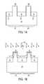
- FIG. 1Ashows an integrated circuit structure, in accordance with some embodiments.
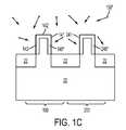
- FIG. 1Bshows dopant ions being directed toward a substrate and implanted into fin structures to form implanted regions, in accordance with some embodiments.
- FIG. 1Cshows dopant plasma ions directed toward a substrate and implanted into fin structures to form implanted regions, in accordance with some embodiments.
- FIG. 2Ashows two dopant profiles for two substrates with two different orientations by using a plasma doping process, in accordance with some embodiments.
- FIG. 2Bshows RF power for pulsed plasma as a function of time, in accordance with some embodiments.
- FIG. 2Cshows two dopant profiles for two substrates with two different orientations by using another plasma doping process, in accordance with some embodiments.
- FIG. 2Dshows resistivity of fin structures as a function of process time by using the plasma implantation process of FIG. 2C , in accordance with some embodiments.
- FIG. 2Eshows resistivity of fin structures as a function of process time by using the plasma implantation process of FIG. 2A , in accordance with some embodiments.
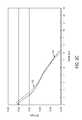
- FIG. 3shows two dopant profiles for two substrates with two different orientations by using a two-step plasma implantation process, in accordance with some embodiments.
- FIGS. 4A-4Dcompare electrical results of fin structures for three different processes, in accordance with some embodiments.
- FIG. 1Ashows an integrated circuit structure 10 , in accordance with some embodiments.
- the illustrated integrated circuit structure 10is formed on a portion of a substrate 20 .
- Substrate 20may be a silicon substrate, a germanium substrate, or a substrate formed of other semiconductor materials.
- Substrate 20may be doped with a p-type or an n-type impurity.
- Isolation regions, such as shallow trench isolation (STI) regions 22may be formed in or over substrate 20 .
- Semiconductor fins 124 and 224are formed above surfaces 23 of STI regions 22 .
- substrate 20includes two PMOS (P-type metal-oxide-semiconductor) device regions 100 and 200 , and semiconductor fins 124 and 224 in the PMOS regions respectively, as shown in FIG. 1A .
- device regions 100 and 200are for NMOS (N-type MOS) devices.
- device region 100is for an NMOS device and device region 200 is for a PMOS device, or vice versa.
- semiconductor fins 124 and 224are formed by creating (or forming) shallow trench isolation (STI) regions 22 , and recessing the top surface of STI regions 22 to a level lower than the original top surface of substrate 20 . The remaining portions of substrate 20 between STI regions 22 thus become fins 124 and 224 .
- semiconductor fins 124 and 224are formed of a material different from that of substrate 20 . They can be formed by recessing top portions of substrate 20 between neighboring STI regions 22 to form recesses, and re-growing a semiconductor material different from that of substrate 20 in the recesses. Top portions of STI regions 22 may then be removed, while bottom portions of STI regions 22 are not removed. As a result, the top portions of the re-grown semiconductor material between neighboring STI regions 22 become semiconductor fins 124 , 224 .
- STIshallow trench isolation
- FIG. 1Bshows P-type dopant ions 150 , such as boron (B) ions, being directed toward substrate 20 and implanted into fins 124 and 224 to form implanted regions 148 and 248 , in accordance with some embodiments.
- the dopants, which are ions,may be directed toward substrate 20 vertically, or tilted toward the sidewalls of fins 124 ad 224 at an angle “ ⁇ ”.
- the dopant profiles of implanted regions 148 and 248are not uniform beneath the outer profiles 141 , 241 (denoted with bold lines) of fins 124 and 224 respectively.
- Such uneven dopant profiles of implanted regions 148 , 248 and other similar regionsare more pronounced for advanced device technologies with high aspect ratios in the spaces between fins.
- the uneven dopant profileswould be maintained after dopant diffusion and would result in variation in device performance within a die (WID). Further, for advanced device technologies, such as technology nodes below 90 nanometers (nm), junction depth shallower than about 25 nm could be needed.
- such shallow junction depthis used for FinFET (fin field effect transistor) structures with high aspect ratios, such as aspect ratios equal to or greater than about 1.3 for 22 nm technology nodes, in accordance with some embodiments.
- Doping by ion beamsfails to achieve the requirement of shallow junction depth due to the relatively high energy of ion beams. As a result, new doping mechanisms are needed.
- FIG. 1Cshows P-type dopant ions 150 *, such as boron (B) ions, in the plasma sheath (whose boundary is not shown) right above the surface of substrate 20 , directed toward substrate 20 and implanted into fins 124 and 224 to form implanted regions 148 * and 248 * respectively, in accordance with some embodiments.
- the method of dopingis called “Plasma doping” (PLAD).
- PLDP-type dopant ions 150 *, such as boron (B) ions, in the plasma sheath (whose boundary is not shown) right above the surface of substrate 20 , directed toward substrate 20 and implanted into fins 124 and 224 to form implanted regions 148 * and 248 * respectively, in accordance with some embodiments.
- the method of dopingis called “Plasma doping” (PLAD).
- the dopant plasma ions 150 *arrive at the substrate surface in a range of angles, instead of being at a certain angle as in the case
- the dopant profiles 148 * and 248 *are more uniform beneath the outer profiles 141 , 241 of semiconductor fins 124 , 224 . Since the plasma ions have lower energy than the ions of ion beams, shallow junction depth (such as less than about 25 nm) can be achieved.
- Semiconductor fins 124 and 224are made of crystalline or epitaxial materials.
- the top surfaces 142 and sidewall surfaces 143have different crystalline orientation.
- the top surfaces 142could be in [100] orientation and the sidewall surfaces 143 could be in [110] orientation.
- Crystalline surfaces with different orientationscould be doped at different rates.
- FIG. 2Ashows a dopant profile 201 for a substrate with an [100] orientation on the substrate surface and a dopant profile 202 for another substrate with an [110] orientation on the substrate surface, in accordance with some embodiments.
- the measurementis taken by secondary ion mass spectroscopy (SIMS).
- Both substratesare doped by plasma doping (PLAD) with boron.
- the plasma dopingwas performed in a plasma doping system.
- An example of plasma doping systemsis a PLAD system, made by Varian Semiconductor Equipment Associates Inc. of Gloucester, Massachusetts.
- the doping gasis made by diluting a reactant gas mixture (15% B 2 H 6 and 85% H 2 ), diluted by a carrier (or dilution) gas H 2 .
- the ratio of the reactant gas to the carrier gasis about 49/80.
- the pressure of the plasma processis about 50 mTorr and RF (radio frequency) power is in a range from about 100 watts (W) to about 1000 W and at a radio frequency in a range from about 2 kilohertz (KHz) to about 13.6 megahertz (MHz).
- the substrateis not biased.
- the radio frequency (RF) power for generating the plasmacould be pulsed.
- FIG. 2Bshows a diagram of power cycle of a pulsed plasma, in accordance with some embodiments.
- FIG. 2Bshows that the RF power is turned on and off periodically.
- the duty ratio (power-on-time/total-time) of pulsecould be in a range from about 5% to about 100%, in accordance with some embodiments.
- the plasma dopingwas performed for equal to or less than about 5 minutes. The results are taken after plasma doping and also after a rapid thermal annealing (RTA) at 950° C. for less than about 5 seconds.
- RTArapid thermal annealing
- junction depth, Xjis about 16.5 nm for the substrate with [110] surface and about 18.9 nm for the substrate with [100] surface.
- Junction depth, Xjis measured at dopant level of about 5E18 atoms/cm 3 . Both junction depths, Xj, are less than the 25 nm, as required for advanced device technologies.
- the difference in junction depth, Xj, at [100] crystalline orientation (top surface) and at [110] crystalline orientation (sidewall surface)indicates a dependence of doping rate on the crystalline orientation.
- FIG. 2Cshows a dopant profile 211 for a substrate with an [100] orientation on the substrate surface and a dopant profile 212 (dotted line) for another substrate with an [110] orientation on the substrate surface, in accordance with some embodiments.
- the dopantsare also boron.
- the process gas used in collecting data in FIG. 2Cis similar with the exception that the carrier gas is Ar, instead of H 2 .
- the resultsshow that the junction depths, Xj, for both substrates are very close and both are at about 11 nm.
- Aras a carrier gas, the dependence of the junction depth with substrate crystalline orientation disappears. The independence of junction depth from substrate crystalline orientation is more desirable for fin structures with different crystalline orientation of different surfaces of the fins.
- FIG. 2Dshows the resistivity data taken from the substrates of FIG. 2C (Ar as the carrier gas), in accordance with some embodiments.
- the resistivity dataare taken from diffusion regions after the substrates are plasma doped with boron and are annealed. The data show that the resistivity varies significantly with the process time, which indicates very limited region(s) to produce repeatable results.
- FIG. 2Eshows the resistivity data taken from the substrate of FIG. 2A (H 2 as the carrier gas), in accordance with some embodiments. The data show that the resistivity is stable between about 120 seconds to about 250 seconds of process time, which is a fairly wide process window.
- FIGS. 2 A and 2 C- 2 Eshow that using Ar as a carrier gas removes the dependence of doping rate on crystalline orientation of the surface (i.e. [100] surface versus [110] surface).
- the resistivity datashow that the process window of such process is too narrow to produce repeatable results.
- the process window of the process using H 2 as a carrier (or dilution) gasis much wider and usable to produce repeatable results.
- the process of using H 2 as a carrier gasshows a dependence of doping rate on the crystalline orientation of the substrate.
- FIG. 3shows dopant profiles 301 (data with square symbol) and 302 (data with triangle symbol) for substrates with [100] surface orientation and [110] surface orientation respectively, in accordance with some embodiments.
- the plasma doping (PLAD) process used to generate the data in FIG. 3uses a two-step process.
- the two-step processincludes a first plasma doping process using Ar as a carrier gas to eliminate or reduce the dependence of doping rate on the crystalline orientation.
- the process condition and gas mixture for the first plasma doping process using Ar as a carrier gashas been described above for FIGS. 2C and 2D .
- the second plasma doping processuses H 2 as a carrier gas to achieve repeatable doping profiles from wafer to wafer, which has been described above for FIGS. 2A and 2E .
- the first plasma dopingis performed for a duration in a range from about 10 seconds to about 100 seconds and the second plasma doping is performed for a duration in a range from about 10 seconds to about 300 seconds. In some embodiments, the duration for the second plasma is shorter than the duration of the first plasma.
- the data in FIG. 3are taken after the 2-step plasma doping process and also a 950° C. thermal anneal. The thermal anneal is performed in a rapid thermal annealing system at peak temperature (950° C.) for equal to or less than about 5 seconds.
- Dopant profiles 301 and 302match pretty closely along the entire curves.
- the junction depth, Xj, for the substrate with [100] surfaceis measured to be about 12.6 nm, and the junction depth for the substrate with [110] surface is measured to be about 13.7 nm.
- the two junction depthsare fairly close.
- the first-step doping plasma process using a relatively heavy carrier gas, such as Ar (atomic weight 40 amu) or Ne (atomic weight 20 amu)likely bombards the crystalline surface to make the substrate surface slightly amorphous, which eliminates or reduces the dependence of doping rate on crystalline orientation.
- the slightly amorphous surfaceallows the second-step doping process with a lighter carrier gas, such as H 2 or He, to deliver dopants deeper into the substrate repeatably.
- the slightly amorphous substrate surfacecan be re-crystallized again by the following annealing process(es) and does not impact the performance of the FETs.
- FIG. 4Ashows data of Isoff (nA/ ⁇ m) versus Idsat (nA/ ⁇ m), in accordance with some embodiments.
- Isoffmeasures the current (off current) when the gate voltage (Vg) is set at zero
- Idsatmeasures the current (on current at saturation region) when the source voltage (Vs) is set at zero.
- the dataare taken from finFET devices on substrates processed with three different processes.
- the 1 st processis a reference process using the conventional ion beams to drive dopants. The results of the 1 st process are marked by “diamond” symbol.
- the 2 nd processis a two-step plasma doping process described above with bias voltage set at 0 volt (no bias).
- the results of the 2 nd processare marked by “square” symbol.
- the 3 nd processis a two-step plasma doping process described above with bias voltage set at 0.3 KV (no bias).
- the results of the 3 nd processare marked by “triangle” symbol.
- the 3 rd processis similar to the 2 nd process with the exception that the bias voltage is 0.3 KV with the substrate being negatively biased.
- the Idsatis measured at Isoff equal to about 100 nA/ ⁇ m. The results show that the Idsat is about 665.4 nA/ ⁇ m for the 1 st process, about 702.4 for the 2 nd process and about 678.9 for the 3 rd process.
- the Idsat of the 1 st processis the lowest and the Idsat of the 2 rd process is the highest.
- the 2 nd processincreases Idsat by about 5.6% over the reference process (1st process).
- the 3 rd processincreases Idsat by about 2.0% over the reference process.
- the resultsindicate an improvement in Idsat by using a plasma doping process, especially a plasma doping process without bias voltage.
- FIG. 4Bshows the Idsat as a function of gate length (or gate width), in accordance with some embodiments.
- Lmaskis the layout gate length, which could be different from actual gate lengths. However, the actual gate lengths increase with the layout gate lengths.
- the data in FIG. 4Bshow that Idsat of the 2 nd process is consistently higher than the Idsat of the 1 st and 3 rd processes for different gate lengths between about 0.03 ⁇ m to about 0.055 ⁇ m.
- FIG. 4Cshows Vtlin and Vtsat versus layout gate length (Lmask), in accordance with some embodiments.
- Vtlinis a measure of the gate voltage when the drain current is measurable and when the Vsource is set at zero and the Vdrain is set at 0.05V.
- Vtsatis a measure of the gate voltage when the drain voltage is measurable and when the Vsource is set at zero and the Vdrain is set at high value (such as greater than about 0.5 V, i.e. at saturation).
- the datashow no significant difference of Vtlin and Vtsat between 3 different processes with gate widths between about 0.022 nm to about 0.1 nm.
- FIG. 4Dshows the resistance of FinFET devices as a function of gate length (L_TEM) of the measured FinFET devices, in accordance with some embodiments.
- L_TEMis a gate length calibrated by a transmission electron microscope (TEM).
- the data in FIG. 4 Dshow resistivities for the 3 doping methods with data analyzed into linear lines and equations. The resistivity data for the 3 doping methods vary linearly with gate length.
- Rs (1 St Process)5397.7 ⁇ L — TEM+ 230.9
- Rs (2 nd Process)5255.9 ⁇ L — TEM+ 229.8
- Rs (3 rd Process)5347.5 ⁇ L — TEM+ 246.5 (3)
- resultsshow no abnormality of resistances and mobilities of dopants of FinFET devices for these 3 doping methods.
- the slopes of equationsare inversely proportional to the mobility (1/ ⁇ ) of dopants.
- resultsshow that dopants for the 2 nd process (plasma doping with zero bias) have the highest mobility in comparison to the other two processes.
- the resultsalso indicate that the 2-step plasma doping process can be used as a doping process.
- the plasma doping methods and results described aboveindicate that a 2-step plasma doping processes have good process windows and produce good device performance data.
- the plasma doping process with zero biasproduces better Idsat data than the process with a bias of about 0.3 KV.
- Both plasma doping processes, with zero bias and 0.3 KV biasshow better doping performance than the conventional ion beam doping process.
- the annealing temperature used in the study aboveis about 950° C.
- the annealing temperature for LDD formationcan be in a range from about 900° C. to about 1350° C. for a duration from milliseconds (ms) to minutes.
- the plasmamay be pulsed with duty ratio in a range from about 5% to about 100%.
- the RF power frequencymay be in a range from about 2 KHz to about 13.6 MHz. In some embodiments, the RF power supply can have dual frequencies.
- the doping plasmamay be generated in the processing chamber or remotely (remote plasma).
- the annealing process used for collecting data in FIGS. 2 A and 2 C- 4 Dis rapid thermal annealing (RTA).
- RTArapid thermal annealing
- the annealing processcan be laser anneal or flash anneal.
- the annealing timecan be in a range from about 50 ⁇ s (micro seconds) to about 10 minutes.
- the doping gas in the exampleis a mixture of 15% H 2 B 6 with 85% of H 2 . Other ratios of gas mixtures may also be used.
- the boron containing gasdoes not need to be H 2 B 6 .
- Other types of boron-containing gas, such as BF 3may also be used.
- the boron-containing gasdoes not need to be mixed with H 2 .
- N 2may also be a carrier gas.
- heavier carrier gassuch as Ne, Ar, Kr, Xe, N 2
- lighter carrier gassuch as He or H 2
- He or H 2may be used for preparing the gas mixture for the second-step plasma doping process.
- the dopant-containing gas used in the first doping plasmawhich makes the substrate surface slightly amorphous and doping process less sensitive to crystalline orientation of the substrate, is different from the dopant-containing gas used in the second doping plasma, which is used to drive the dopants deeper into the substrate.
- the dopantis boron
- the dopant-containing gas used in the first doping plasmacould be B 2 H 6 and the dopant-containing gas used in the second doping plasma could be BF 3 , or vice versa.
- the bias voltage applied on the substratemay also be turned on and off periodically to modify the doping characteristics in a manner similar to RF power being turned on and off to generate pulsed plasma, as shown in FIG. 2B .
- the duty ratio (power-on-time/total-time) of bias pulsecould also be in a range from about 5% to about 100%, in accordance with some embodiments.
- the embodiments of methods and structures described above for doping fin structures by plasma doping processenable formation shallow lightly doped source and drain (LDD).
- the methodsinvolve a two-step plasma doping process.
- the first step plasma processuses a heavy carrier gas, such as a carrier gas with an atomic weight equal to or greater than about 20 amu, to make the surfaces of fin structures amorphous and to reduce the dependence of doping rate on crystalline orientation.
- the second step plasma processuses a lighter carrier gas, which is lighter than the carrier gas for the first step plasma process, to drive the dopants deeper into the fin structures.
- the two-step plasma doping processproduces uniform dopant profile beneath the outer surfaces of the fin structures.
- a method of doping a shallow lightly doped source and drain (LDD) regions of fin structures on a substrateincludes applying a first doping plasma on the shallow LDD regions of the fin structures.
- the fin structureshave surfaces with more than one crystalline orientation, and a first source gas of the first doping plasma includes a first dopant-containing gas and a first carrier gas, wherein the first dopant-containing gas includes the dopant.
- the doping rate of the first doping plasmais significantly the same on different surfaces of the fin structures with more than one crystalline orientation.
- the methodalso includes applying a second doping plasma on the shallow LDD regions of the fin structures after the first doping plasma is applied.
- a second source gas of the second doping plasmaincludes a second dopant-containing gas and a second carrier gas, and the second doping plasma delivers the dopant deeper below surfaces of the shallow LDD regions of the fin structures.
- a method of doping a shallow lightly doped source and drain (LDD) regions of fin structures on a substrateincludes applying a first doping plasma on the shallow LDD regions of the fin structures, and the fin structures have surfaces with more than one crystalline orientation.
- a first source gas of the first doping plasmaincludes a first dopant-containing gas and a first carrier gas, and the first dopant-containing gas includes the dopant.
- the doping rate of the first doping plasmais significantly the same on different surfaces of the fin structures with more than one crystalline orientation.
- the methodfurther includes applying a second doping plasma on the shallow LDD regions of the fin structures after the first doping plasma is applied.
- a second source gas of the second doping plasmaincludes a second dopant-containing gas and a second carrier gas.
- the second doping plasmadelivers the dopant deeper below surfaces of the shallow LDD regions of the fin structures, and the dopant profiles of the shallow LDD regions are uniform beneath the outer profiles of the fin structures.
- the methodincludes performing a thermal annealing on the substrate after the second doping plasma is applied.
- a fin field-effect transistorhaving a fin structure with a shallow lightly doped source and drain (LDD) region.
- the fin structurehas a top surface with a first crystalline orientation.
- Two sidewall surfaces of the fin structurehave a second crystalline orientation.
- the shallow LDD regionis uniform beneath the top surface and the two sidewall surfaces of the fin structure, and dopants in the shallow LDD region are implanted in the fin structure by a two-step plasma doping process.
- a first step plasma doping process of the two-step plasma doping processuses a carrier gas with an atomic weight equal to or greater than 20 amu, and the first step plasma doping process makes the top surface and the two sidewall surfaces amorphous to reduce the difference in crystalline orientation of surfaces of the fin structure to enable dopants to be implanted uniformly beneath the surfaces of the fin structures by the second-step plasma doping process.
Landscapes
- Engineering & Computer Science (AREA)
- Physics & Mathematics (AREA)
- Plasma & Fusion (AREA)
- Condensed Matter Physics & Semiconductors (AREA)
- General Physics & Mathematics (AREA)
- Manufacturing & Machinery (AREA)
- Computer Hardware Design (AREA)
- Microelectronics & Electronic Packaging (AREA)
- Power Engineering (AREA)
- Insulated Gate Type Field-Effect Transistor (AREA)
Abstract
Description
The present application is related to U.S. patent application Ser. Nos. 12/707,788, filed on Feb. 18, 2010, titled MEMORY POWER GATING CIRCUIT AND METHODS; Ser. No. 12/758,426, filed on Apr. 12, 2010, titled FINFETS AND METHODS FOR FORMING THE SAME; Ser. No. 12/731,325, filed on Mar. 25, 2010, titled ELECTRICAL FUSE AND RELATED APPLICATIONS; Ser. No. 12/724,556, filed on Mar. 16, 2010, titled ELECTRICAL ANTI-FUSE AND RELATED APPLICATIONS; Ser. No. 12/757,203, filed on Apr. 9, 2010, titled STI STRUCTURE AND METHOD OF FORMING BOTTOM VOID IN SAME; Ser. No. 12/797,839, filed on Jun. 10, 2010, titled FIN STRUCTURE FOR HIGH MOBILITY MULTIPLE-GATE TRANSISTOR; Ser. No. 12/831,842, filed on Jul. 7, 2010, titled METHOD FOR FORMING HIGH GERMANIUM CONCENTRATION SiGe STRESSOR; Ser. No. 12/761,686, filed on Apr. 16, 2010, titled FINFETS AND METHODS FOR FORMING THE SAME; Ser. No. 12/766,233, filed on Apr. 23, 2010, titled FIN FIELD EFFECT TRANSISTOR; Ser. No. 12/757,271, filed on Apr. 9, 2010, titled ACCUMULATION TYPE FINFET, CIRCUITS AND FABRICATION METHOD THEREOF; Ser. No. 12/694,846, filed on Jan. 27, 2010, titled INTEGRATED CIRCUITS AND METHODS FOR FORMING THE SAME; Ser. No. 12/638,958, filed on Dec. 14, 2009, titled METHOD OF CONTROLLING GATE THICKNESS IN FORMING FINFET DEVICES; Ser. No. 12/768,884, filed on Apr. 28, 2010, titled METHODS FOR DOPING FIN FIELD-EFFECT TRANSISTORS; Ser. No. 12/731,411, filed on Mar. 25, 2010, titled INTEGRATED CIRCUIT INCLUDING FINFETS AND METHODS FOR FORMING THE SAME; Ser. No. 12/775,006, filed on May 6, 2010, titled METHOD FOR FABRICATING A STRAINED STRUCTURE; Ser. No. 12/886,713, filed Sep. 21, 2010, titled METHOD OF FORMING INTEGRATED CIRCUITS; Ser. No. 12/941,509, filed Nov. 8, 2010, titled MECHANISMS FOR FORMING ULTRA SHALLOW JUNCTION; Ser. No. 12/900,626, filed Oct. 8, 2010, titled TRANSISTOR HAVING NOTCHED FIN STRUCTURE AND METHOD OF MAKING THE SAME; Ser. No. 12/903,712, filed Oct. 13, 2010, titled FINFET AND METHOD OF FABRICATING THE SAME; 61/412,846, filed Nov. 12, 2010, 61/394,418, filed Oct. 19, 2010, titled METHODS OF FORMING GATE DIELECTRIC MATERIAL and 61/405,858, filed Oct. 22, 2010, titled METHODS OF FORMING SEMICONDUCTOR DEVICES.
This disclosure relates generally to integrated circuit devices and more particularly to processes of doping for field-effect transistors (FETs).
Semiconductor integrated circuit microelectronic fabrications are formed from semiconductor substrates within and upon which are formed semiconductor devices. Patterned conductor layers separated by dielectric layers are then formed over the semiconductor substrates to provide interconnect. Ubiquitous within the fabrication of semiconductor integrated circuit microelectronic fabrications is the use of field effect transistor (FET) devices as switching devices within both logic semiconductor integrated circuit microelectronic fabrications and memory semiconductor integrated circuit microelectronic fabrications. The accelerated shrinking of FET dimensions poses particular challenges for doping processes used in transistor fabrication. Dopant ion implantation by ion beams has widely been used to locally modify the electrical properties of silicon. However, ion implantation by ion beams has its limitations for meeting specifications of advanced devices.
The present disclosure will be readily understood by the following detailed description in conjunction with the accompanying drawings, and like reference numerals designate like structural elements.
It is to be understood that the following disclosure provides many different embodiments, or examples, for implementing different features of the invention. Specific examples of components and arrangements are described below to simplify the present disclosure. These are, of course, merely examples and are not intended to be limiting. In addition, the present disclosure may repeat reference numerals and/or letters in the various examples. This repetition is for the purpose of simplicity and clarity and does not in itself dictate a relationship between the various embodiments and/or configurations discussed.
In some embodiments,semiconductor fins regions 22, and recessing the top surface ofSTI regions 22 to a level lower than the original top surface ofsubstrate 20. The remaining portions ofsubstrate 20 betweenSTI regions 22 thus becomefins semiconductor fins substrate 20. They can be formed by recessing top portions ofsubstrate 20 between neighboringSTI regions 22 to form recesses, and re-growing a semiconductor material different from that ofsubstrate 20 in the recesses. Top portions ofSTI regions 22 may then be removed, while bottom portions ofSTI regions 22 are not removed. As a result, the top portions of the re-grown semiconductor material between neighboringSTI regions 22 becomesemiconductor fins
Afterfins substrate 20 undergoes additional substrate processing to form FET devices. One operation in forming FET devices is doping the lightly doped source and drain (LDD) regions. Conventional LDD doping is performed by ion implantation with the assistance of ion beams.FIG. 1B shows P-type dopant ions 150, such as boron (B) ions, being directed towardsubstrate 20 and implanted intofins regions substrate 20 vertically, or tilted toward the sidewalls offins 124ad 224 at an angle “α”. Due to shadowing effect, the dopant profiles of implantedregions outer profiles 141,241 (denoted with bold lines) offins regions
The radio frequency (RF) power for generating the plasma could be pulsed.FIG. 2B shows a diagram of power cycle of a pulsed plasma, in accordance with some embodiments.FIG. 2B shows that the RF power is turned on and off periodically. The duty ratio (power-on-time/total-time) of pulse could be in a range from about 5% to about 100%, in accordance with some embodiments. The plasma doping was performed for equal to or less than about 5 minutes. The results are taken after plasma doping and also after a rapid thermal annealing (RTA) at 950° C. for less than about 5 seconds. The results show the junction depth, Xj, is about 16.5 nm for the substrate with [110] surface and about 18.9 nm for the substrate with [100] surface. Junction depth, Xj, is measured at dopant level of about 5E18 atoms/cm3. Both junction depths, Xj, are less than the 25 nm, as required for advanced device technologies. The difference in junction depth, Xj, at [100] crystalline orientation (top surface) and at [110] crystalline orientation (sidewall surface) indicates a dependence of doping rate on the crystalline orientation.
In addition to the consideration of achieving shallow junction depth (less than about 25 nm) and independence of doping rate on crystalline orientation, a doping process also needs to be repeatable.FIG. 2D shows the resistivity data taken from the substrates ofFIG. 2C (Ar as the carrier gas), in accordance with some embodiments. The resistivity data are taken from diffusion regions after the substrates are plasma doped with boron and are annealed. The data show that the resistivity varies significantly with the process time, which indicates very limited region(s) to produce repeatable results. In contrast,FIG. 2E shows the resistivity data taken from the substrate ofFIG. 2A (H2as the carrier gas), in accordance with some embodiments. The data show that the resistivity is stable between about 120 seconds to about 250 seconds of process time, which is a fairly wide process window.
The data in FIGS.2A and2C-2E show that using Ar as a carrier gas removes the dependence of doping rate on crystalline orientation of the surface (i.e. [100] surface versus [110] surface). However, the resistivity data show that the process window of such process is too narrow to produce repeatable results. In contrast, the process window of the process using H2as a carrier (or dilution) gas is much wider and usable to produce repeatable results. However, the process of using H2as a carrier gas shows a dependence of doping rate on the crystalline orientation of the substrate.
Dopant profiles301 and302 match pretty closely along the entire curves. The junction depth, Xj, for the substrate with [100] surface is measured to be about 12.6 nm, and the junction depth for the substrate with [110] surface is measured to be about 13.7 nm. The two junction depths are fairly close. The first-step doping plasma process using a relatively heavy carrier gas, such as Ar (atomic weight 40 amu) or Ne (atomic weight 20 amu), likely bombards the crystalline surface to make the substrate surface slightly amorphous, which eliminates or reduces the dependence of doping rate on crystalline orientation. The slightly amorphous surface allows the second-step doping process with a lighter carrier gas, such as H2or He, to deliver dopants deeper into the substrate repeatably. The slightly amorphous substrate surface can be re-crystallized again by the following annealing process(es) and does not impact the performance of the FETs.
Rs(1StProcess)=5397.7×L—TEM+230.9 (1)
Rs(2ndProcess)=5255.9×L—TEM+229.8 (2)
Rs(3rdProcess)=5347.5×L—TEM+246.5 (3)
The results show no abnormality of resistances and mobilities of dopants of FinFET devices for these 3 doping methods. The slopes of equations are inversely proportional to the mobility (1/μ) of dopants. The results show that dopants for the 2ndprocess (plasma doping with zero bias) have the highest mobility in comparison to the other two processes. The results also indicate that the 2-step plasma doping process can be used as a doping process.
The plasma doping methods and results described above indicate that a 2-step plasma doping processes have good process windows and produce good device performance data. The plasma doping process with zero bias produces better Idsat data than the process with a bias of about 0.3 KV. Both plasma doping processes, with zero bias and 0.3 KV bias, show better doping performance than the conventional ion beam doping process.
The annealing temperature used in the study above is about 950° C. Alternatively, the annealing temperature for LDD formation can be in a range from about 900° C. to about 1350° C. for a duration from milliseconds (ms) to minutes. As mentioned above, the plasma may be pulsed with duty ratio in a range from about 5% to about 100%. The RF power frequency may be in a range from about 2 KHz to about 13.6 MHz. In some embodiments, the RF power supply can have dual frequencies. The doping plasma may be generated in the processing chamber or remotely (remote plasma).
The annealing process used for collecting data in FIGS.2A and2C-4D is rapid thermal annealing (RTA). Alternatively, the annealing process can be laser anneal or flash anneal. The annealing time can be in a range from about 50 μs (micro seconds) to about 10 minutes. The doping gas in the example is a mixture of 15% H2B6with 85% of H2. Other ratios of gas mixtures may also be used. In addition, the boron containing gas does not need to be H2B6. Other types of boron-containing gas, such as BF3, may also be used. The boron-containing gas does not need to be mixed with H2. Other types of inert gas, such as He, Ar, Ne, Kr, Xe, may also be used. In some embodiments, N2may also be a carrier gas. However, heavier carrier gas, such as Ne, Ar, Kr, Xe, N2, may be used to prepare the gas mixture for the first-step plasma doping process and lighter carrier gas, such as He or H2, may be used for preparing the gas mixture for the second-step plasma doping process.
In some embodiments, the dopant-containing gas used in the first doping plasma, which makes the substrate surface slightly amorphous and doping process less sensitive to crystalline orientation of the substrate, is different from the dopant-containing gas used in the second doping plasma, which is used to drive the dopants deeper into the substrate. For example, if the dopant is boron, the dopant-containing gas used in the first doping plasma could be B2H6and the dopant-containing gas used in the second doping plasma could be BF3, or vice versa. The bias voltage applied on the substrate may also be turned on and off periodically to modify the doping characteristics in a manner similar to RF power being turned on and off to generate pulsed plasma, as shown inFIG. 2B . The duty ratio (power-on-time/total-time) of bias pulse could also be in a range from about 5% to about 100%, in accordance with some embodiments.
The embodiments of methods described above for doping a substrate to form shallow LDD regions are described for PMOS. Similar methods also apply for NMOS, which uses N-type dopants, such as P and As. Phosphorous-containing or As-containing gas may be used for the doping LDD regions in manner described above for using boron-containing gas to dope P-type LDD.
The embodiments of methods and structures described above for doping fin structures by plasma doping process enable formation shallow lightly doped source and drain (LDD). The methods involve a two-step plasma doping process. The first step plasma process uses a heavy carrier gas, such as a carrier gas with an atomic weight equal to or greater than about 20 amu, to make the surfaces of fin structures amorphous and to reduce the dependence of doping rate on crystalline orientation. The second step plasma process uses a lighter carrier gas, which is lighter than the carrier gas for the first step plasma process, to drive the dopants deeper into the fin structures. The two-step plasma doping process produces uniform dopant profile beneath the outer surfaces of the fin structures.
In one embodiment, a method of doping a shallow lightly doped source and drain (LDD) regions of fin structures on a substrate is provided. The method includes applying a first doping plasma on the shallow LDD regions of the fin structures. The fin structures have surfaces with more than one crystalline orientation, and a first source gas of the first doping plasma includes a first dopant-containing gas and a first carrier gas, wherein the first dopant-containing gas includes the dopant. The doping rate of the first doping plasma is significantly the same on different surfaces of the fin structures with more than one crystalline orientation. The method also includes applying a second doping plasma on the shallow LDD regions of the fin structures after the first doping plasma is applied. A second source gas of the second doping plasma includes a second dopant-containing gas and a second carrier gas, and the second doping plasma delivers the dopant deeper below surfaces of the shallow LDD regions of the fin structures.
In another embodiment, a method of doping a shallow lightly doped source and drain (LDD) regions of fin structures on a substrate is provided. The method includes applying a first doping plasma on the shallow LDD regions of the fin structures, and the fin structures have surfaces with more than one crystalline orientation. A first source gas of the first doping plasma includes a first dopant-containing gas and a first carrier gas, and the first dopant-containing gas includes the dopant. The doping rate of the first doping plasma is significantly the same on different surfaces of the fin structures with more than one crystalline orientation. The method further includes applying a second doping plasma on the shallow LDD regions of the fin structures after the first doping plasma is applied. A second source gas of the second doping plasma includes a second dopant-containing gas and a second carrier gas. The second doping plasma delivers the dopant deeper below surfaces of the shallow LDD regions of the fin structures, and the dopant profiles of the shallow LDD regions are uniform beneath the outer profiles of the fin structures. In addition, the method includes performing a thermal annealing on the substrate after the second doping plasma is applied.
In yet another embodiment, a fin field-effect transistor (FinFET) having a fin structure with a shallow lightly doped source and drain (LDD) region is provided. The fin structure has a top surface with a first crystalline orientation. Two sidewall surfaces of the fin structure have a second crystalline orientation. The shallow LDD region is uniform beneath the top surface and the two sidewall surfaces of the fin structure, and dopants in the shallow LDD region are implanted in the fin structure by a two-step plasma doping process. A first step plasma doping process of the two-step plasma doping process uses a carrier gas with an atomic weight equal to or greater than 20 amu, and the first step plasma doping process makes the top surface and the two sidewall surfaces amorphous to reduce the difference in crystalline orientation of surfaces of the fin structure to enable dopants to be implanted uniformly beneath the surfaces of the fin structures by the second-step plasma doping process.
Various modifications, changes, and variations apparent to those of skill in the art may be made in the arrangement, operation, and details of the methods and systems disclosed. Although the foregoing invention has been described in some detail for purposes of clarity of understanding, it will be apparent that certain changes and modifications may be practiced within the scope of the appended claims. Accordingly, the present embodiments are to be considered as illustrative and not restrictive, and the invention is not to be limited to the details given herein, but may be modified within the scope and equivalents of the appended claims.
Claims (20)
1. A method of doping shallow lightly doped source and drain (LDD) regions of fin structures on a substrate, comprising:
applying a first doping plasma on the shallow LDD regions of the fin structures, wherein the fin structures have surfaces with more than one crystalline orientation, wherein a first source gas of the first doping plasma includes a first dopant-containing gas and a first carrier gas, wherein the first dopant-containing gas includes the dopant, wherein the doping rate of the first doping plasma is significantly the same on different surfaces of the fin structures with more than one crystalline orientation; and
applying a second doping plasma on the shallow LDD regions of the fin structures after the first doping plasma is applied; wherein a second source gas of the second doping plasma includes a second dopant-containing gas and a second carrier gas, wherein the second doping plasma delivers the dopant deeper below surfaces of the shallow LDD regions of the fin structures.
2. The method ofclaim 1 , further comprising:
performing a thermal annealing on the substrate after the second doping plasma is applied.
3. The method ofclaim 2 , wherein the temperature of the thermal annealing is in a range from about 900° C. to about 1350° C.
4. The method ofclaim 1 , wherein the dopant profiles of the shallow LDD regions are uniform beneath outer profiles of the fin structures.
5. The method ofclaim 1 , wherein depths of the shallow LDD regions are less than about 25 nm.
6. The method ofclaim 1 , wherein depths of the shallow LDD regions are less than about 20 nm.
7. The method ofclaim 1 , wherein the dopant is boron, phosphorous, or Arsenic.
8. The method ofclaim 1 , wherein the first and second doping plasmas are generated remotely.
9. The method ofclaim 1 , wherein the first dopant-containing gas and the second dopant-containing gases are both B2H6or both BF3, and wherein both dopant-containing gases are mixed with H2.
10. The method ofclaim 1 , the first carrier gas is selected from a group consisting of Ar, Ne, Kr, Xe, and N2.
11. The method ofclaim 1 , wherein the second carrier gas is He or H2.
12. The method ofclaim 1 , wherein a bias voltage is set to be zero when the first and the second doping plasma are applied.
13. The method ofclaim 1 , wherein a bias voltage is set to be less than about 0.3 KV when the first and the second doping plasma are applied.
14. The method ofclaim 1 , wherein the first doping plasma and the second doping plasma are pulsed plasmas with duty ratios in a range from about 5% to about 100%.
15. The method ofclaim 1 , wherein top surfaces of the fin structures have [100] crystalline orientation and side surface of the fin structures have [110] crystalline orientation.
16. A method of doping shallow lightly doped source and drain (LDD) regions of fin structures on a substrate, comprising:
applying a first doping plasma on the shallow LDD regions of the fin structures, wherein the fin structures have surfaces with more than one crystalline orientation, wherein a first source gas of the first doping plasma includes a first dopant-containing gas and a first carrier gas, wherein the first dopant-containing gas includes the dopant, wherein the doping rate of the first doping plasma is significantly the same on different surfaces of the fin structures with more than one crystalline orientation;
applying a second doping plasma on the shallow LDD regions of the fin structures after the first doping plasma is applied; wherein a second source gas of the second doping plasma includes a second dopant-containing gas and a second carrier gas, wherein the second doping plasma delivers the dopant deeper below surfaces of the shallow LDD regions of the fin structures, and wherein the dopant profiles of the shallow LDD regions are uniform beneath outer profiles of the fin structures; and
performing a thermal annealing on the substrate after the second doping plasma is applied.
17. The method ofclaim 16 , wherein the first dopant-containing gas and the second dopant-containing gas are both B2H6or both BF3, and wherein both dopant-containing gases are mixed with H2.
18. The method ofclaim 16 , wherein the first carrier gas is selected from a group consisting of Ar, Ne, Kr, Xe, and N2, and wherein the second carrier gas is He or H2.
19. A fin field-effect transistor (finFET) having a fin structure with a shallow lightly doped source and drain (LDD) region, comprising:
the fin structure, wherein a top surface of the fin structure has a first crystalline orientation, and wherein two sidewall surfaces of the fin structure have a second crystalline orientation, and wherein the shallow LDD region is uniform beneath the top surface and the two sidewall surfaces of the fin structure, and wherein dopants in the shallow LDD region are implanted in the fin structure by a two-step plasma doping process, and wherein a first step plasma doping process of the two-step plasma doping process uses a carrier gas with an atomic weight equal to or greater than 20 amu, and wherein the first step plasma doping process makes the top surface and the two sidewall surfaces amorphous to reduce the difference in crystalline orientation of surfaces of the fin structure to enable dopants to be implanted uniformly beneath the surfaces of the fin structures by the second-step plasma doping process.
20. The fin structure ofclaim 19 , wherein the first crystalline orientation is [100] and the second crystalline orientation is [110].
Priority Applications (7)
| Application Number | Priority Date | Filing Date | Title |
|---|---|---|---|
| US12/766,233US9484462B2 (en) | 2009-09-24 | 2010-04-23 | Fin structure of fin field effect transistor |
| US12/941,509US8298925B2 (en) | 2010-11-08 | 2010-11-08 | Mechanisms for forming ultra shallow junction |
| US13/650,684US8536658B2 (en) | 2010-11-08 | 2012-10-12 | Mechanisms for forming ultra shallow junction |
| US13/971,181US8735266B2 (en) | 2010-11-08 | 2013-08-20 | Mechanisms for forming ultra shallow junction |
| US14/102,702US9660082B2 (en) | 2009-07-28 | 2013-12-11 | Integrated circuit transistor structure with high germanium concentration SiGe stressor |
| US14/288,158US9048181B2 (en) | 2010-11-08 | 2014-05-27 | Mechanisms for forming ultra shallow junction |
| US15/339,258US10355108B2 (en) | 2009-09-24 | 2016-10-31 | Method of forming a fin field effect transistor comprising two etching steps to define a fin structure |
Applications Claiming Priority (1)
| Application Number | Priority Date | Filing Date | Title |
|---|---|---|---|
| US12/941,509US8298925B2 (en) | 2010-11-08 | 2010-11-08 | Mechanisms for forming ultra shallow junction |
Related Child Applications (1)
| Application Number | Title | Priority Date | Filing Date |
|---|---|---|---|
| US13/650,684ContinuationUS8536658B2 (en) | 2010-11-08 | 2012-10-12 | Mechanisms for forming ultra shallow junction |
Publications (2)
| Publication Number | Publication Date |
|---|---|
| US20120112248A1 US20120112248A1 (en) | 2012-05-10 |
| US8298925B2true US8298925B2 (en) | 2012-10-30 |
Family
ID=46018779
Family Applications (3)
| Application Number | Title | Priority Date | Filing Date |
|---|---|---|---|
| US12/941,509Active2031-04-14US8298925B2 (en) | 2009-07-28 | 2010-11-08 | Mechanisms for forming ultra shallow junction |
| US13/650,684ActiveUS8536658B2 (en) | 2010-11-08 | 2012-10-12 | Mechanisms for forming ultra shallow junction |
| US13/971,181Expired - Fee RelatedUS8735266B2 (en) | 2010-11-08 | 2013-08-20 | Mechanisms for forming ultra shallow junction |
Family Applications After (2)
| Application Number | Title | Priority Date | Filing Date |
|---|---|---|---|
| US13/650,684ActiveUS8536658B2 (en) | 2010-11-08 | 2012-10-12 | Mechanisms for forming ultra shallow junction |
| US13/971,181Expired - Fee RelatedUS8735266B2 (en) | 2010-11-08 | 2013-08-20 | Mechanisms for forming ultra shallow junction |
Country Status (1)
| Country | Link |
|---|---|
| US (3) | US8298925B2 (en) |
Cited By (10)
| Publication number | Priority date | Publication date | Assignee | Title |
|---|---|---|---|---|
| US20120091538A1 (en)* | 2010-10-13 | 2012-04-19 | Taiwan Semiconductor Manufacturing Company, Ltd. | Finfet and method of fabricating the same |
| US20120190167A1 (en)* | 2011-01-25 | 2012-07-26 | Taiwan Semiconductor Manufacturing Company, Ltd. | Mechanisms of doping oxide for forming shallow trench isolation |
| US20120295430A1 (en)* | 2009-04-24 | 2012-11-22 | Varian Semiconductor Equipment Associates, Inc. | Method for processing a substrate having a non-planar substrate surface |
| US8536658B2 (en)* | 2010-11-08 | 2013-09-17 | Taiwan Semiconductor Manufacturing Company, Ltd. | Mechanisms for forming ultra shallow junction |
| US9048181B2 (en) | 2010-11-08 | 2015-06-02 | Taiwan Semiconductor Manufacturing Company, Ltd. | Mechanisms for forming ultra shallow junction |
| US9306038B1 (en) | 2014-12-12 | 2016-04-05 | International Business Machines Corporation | Shallow extension junction |
| US9406675B1 (en)* | 2015-03-16 | 2016-08-02 | Taiwan Semiconductor Manufacturing Company Ltd. | FinFET structure and method of manufacturing the same |
| US9577075B2 (en) | 2013-11-14 | 2017-02-21 | Samsung Electronics Co., Ltd. | Method of manufacturing semiconductor device using plasma doping process and semiconductor device manufactured by the method |
| US20170179254A1 (en)* | 2015-12-18 | 2017-06-22 | International Business Machines Corporation | Channel replacement and bimodal doping scheme for bulk finfet threshold voltage modulation with reduced performance penalty |
| US9812559B2 (en) | 2015-09-03 | 2017-11-07 | Samsung Electronics Co., Ltd. | FINFET semiconductor devices and method of forming the same |
Families Citing this family (19)
| Publication number | Priority date | Publication date | Assignee | Title |
|---|---|---|---|---|
| CN102237945A (en) | 2010-05-06 | 2011-11-09 | 松下电器产业株式会社 | Code division multiplexing method based on quadrature encoding, code division multiplexing equipment and demultiplexing equipment |
| US8716682B2 (en)* | 2011-04-04 | 2014-05-06 | Varian Semiconductor Equipment Associates, Inc. | Apparatus and method for multiple slot ion implantation |
| JP2015037091A (en)* | 2013-08-12 | 2015-02-23 | 東京エレクトロン株式会社 | Etching method |
| US9478659B2 (en) | 2013-10-23 | 2016-10-25 | Taiwan Semiconductor Manufacturing Company, Ltd. | FinFET having doped region and method of forming the same |
| US9653542B2 (en)* | 2013-10-23 | 2017-05-16 | Taiwan Semiconductor Manufacturing Company, Ltd. | FinFET having isolation structure and method of forming the same |
| US20150214331A1 (en)* | 2014-01-30 | 2015-07-30 | Globalfoundries Inc. | Replacement metal gate including dielectric gate material |
| US9553174B2 (en)* | 2014-03-28 | 2017-01-24 | Applied Materials, Inc. | Conversion process utilized for manufacturing advanced 3D features for semiconductor device applications |
| KR102160100B1 (en) | 2014-05-27 | 2020-09-25 | 삼성전자 주식회사 | Method for fabricating semiconductor device |
| US9941406B2 (en) | 2014-08-05 | 2018-04-10 | Taiwan Semiconductor Manufacturing Company, Ltd. | FinFETs with source/drain cladding |
| CN105470135B (en)* | 2014-09-11 | 2018-11-06 | 中国科学院微电子研究所 | Semiconductor device manufacturing method |
| CN105448660B (en)* | 2014-09-30 | 2018-06-29 | 中芯国际集成电路制造(上海)有限公司 | Detect the preparation method of sample and detection sample |
| US9530842B2 (en)* | 2015-01-15 | 2016-12-27 | Micron Technology, Inc. | Semiconductor devices |
| KR102323943B1 (en) | 2015-10-21 | 2021-11-08 | 삼성전자주식회사 | Method of manufacturing semiconductor device |
| KR102530671B1 (en) | 2015-12-31 | 2023-05-10 | 삼성전자주식회사 | Method of fabricating the semiconductor device |
| US10269938B2 (en)* | 2016-07-15 | 2019-04-23 | Taiwan Semiconductor Manufacturing Co., Ltd. | Semiconductor device structure having a doped passivation layer |
| US9899515B1 (en) | 2016-10-31 | 2018-02-20 | International Business Machines Corporation | Fabrication of a pair of vertical fin field effect transistors having a merged top source/drain |
| US10276691B2 (en)* | 2016-12-15 | 2019-04-30 | Taiwan Semiconductor Manufacturing Co., Ltd. | Conformal transfer doping method for fin-like field effect transistor |
| TWI746673B (en)* | 2016-12-15 | 2021-11-21 | 台灣積體電路製造股份有限公司 | Fin-like field effect transistor device and conformal transfer doping method for fin-like field effect transistor |
| CN111052348B (en)* | 2017-09-28 | 2025-05-30 | 英特尔公司 | Transistor having channel and subchannel regions of distinct composition and size |
Citations (143)
| Publication number | Priority date | Publication date | Assignee | Title |
|---|---|---|---|---|
| US5581202A (en) | 1993-11-08 | 1996-12-03 | Hitachi, Ltd. | Semiconductor integrated circuit device and production method thereof |
| US5658417A (en) | 1992-12-08 | 1997-08-19 | Nec Corporation | HF vapor selective etching method and apparatus |
| US5767732A (en) | 1995-06-26 | 1998-06-16 | Samsung Electronics Co., Ltd. | Circuit for permanently adjusting a circuit element value in a semiconductor integrated circuit using fuse elements |
| US5963789A (en) | 1996-07-08 | 1999-10-05 | Kabushiki Kaisha Toshiba | Method for silicon island formation |
| US6065481A (en) | 1997-03-26 | 2000-05-23 | Fsi International, Inc. | Direct vapor delivery of enabling chemical for enhanced HF etch process performance |
| US6121786A (en) | 1997-06-30 | 2000-09-19 | Matsushita Electric Industrial Co., Ltd. | Semiconductor integrated circuit |
| US6503794B1 (en) | 1997-04-10 | 2003-01-07 | Hitachi, Ltd. | Semiconductor integrated circuit device and method for manufacturing the same |
| US20030080361A1 (en) | 2001-11-01 | 2003-05-01 | Anand Murthy | Semiconductor transistor having a stressed channel |
| US6613634B2 (en) | 2000-08-15 | 2003-09-02 | Hitachi, Ltd. | Method of manufacturing a semiconductor device using oblique ion injection |
| US6622738B2 (en) | 2000-10-16 | 2003-09-23 | Micron Technology, Inc. | Apparatus and system for removing photoresist through the use of hot deionized water bath, water vapor and ozone gas |
| US6642090B1 (en) | 2002-06-03 | 2003-11-04 | International Business Machines Corporation | Fin FET devices from bulk semiconductor and method for forming |
| US20030234422A1 (en) | 2002-06-20 | 2003-12-25 | Micron Technology, Inc. | Methods of fabricating a dielectric plug in mosfets to suppress short-channel effects |
| US6706571B1 (en) | 2002-10-22 | 2004-03-16 | Advanced Micro Devices, Inc. | Method for forming multiple structures in a semiconductor device |
| US6727557B2 (en) | 2001-12-07 | 2004-04-27 | Fujitsu Limited | Semiconductor device having well tap provided in memory cell |
| US6740247B1 (en) | 1999-02-05 | 2004-05-25 | Massachusetts Institute Of Technology | HF vapor phase wafer cleaning and oxide etching |
| US6762448B1 (en) | 2003-04-03 | 2004-07-13 | Advanced Micro Devices, Inc. | FinFET device with multiple fin structures |
| US20040192067A1 (en) | 2003-02-28 | 2004-09-30 | Bruno Ghyselen | Method for forming a relaxed or pseudo-relaxed useful layer on a substrate |
| US6828646B2 (en) | 2001-10-17 | 2004-12-07 | Stmicroelectronics Sa | Isolating trench and manufacturing process |
| US6830994B2 (en) | 2001-03-09 | 2004-12-14 | Semiconductor Energy Laboratory Co., Ltd. | Method of manufacturing a semiconductor device having a crystallized semiconductor film |
| US20040259315A1 (en) | 2003-06-09 | 2004-12-23 | Canon Kabushiki Kaisha | Semiconductor substrate, semiconductor device, and method of manufacturing the same |
| US20050020020A1 (en) | 2002-07-16 | 2005-01-27 | Nadine Collaert | Integrated semiconductor fin device and a method for manufacturing such device |
| US6858478B2 (en) | 2002-08-23 | 2005-02-22 | Intel Corporation | Tri-gate devices and methods of fabrication |
| US6872647B1 (en) | 2003-05-06 | 2005-03-29 | Advanced Micro Devices, Inc. | Method for forming multiple fins in a semiconductor device |
| US20050082616A1 (en) | 2003-10-20 | 2005-04-21 | Huajie Chen | High performance stress-enhanced MOSFETs using Si:C and SiGe epitaxial source/drain and method of manufacture |
| US20050153490A1 (en) | 2003-12-16 | 2005-07-14 | Jae-Man Yoon | Method of forming fin field effect transistor |
| US20050170593A1 (en) | 2004-02-02 | 2005-08-04 | Hee-Soo Kang | Method for forming a FinFET by a damascene process |
| US6940747B1 (en) | 2004-05-26 | 2005-09-06 | Hewlett-Packard Development Company, L.P. | Magnetic memory device |
| US6949768B1 (en) | 2004-10-18 | 2005-09-27 | International Business Machines Corporation | Planar substrate devices integrated with finfets and method of manufacture |
| US20050212080A1 (en) | 2004-03-23 | 2005-09-29 | Shien-Yang Wu | Diode junction poly fuse |
| US20050221591A1 (en) | 2004-04-06 | 2005-10-06 | International Business Machines Corporation | Method of forming high-quality relaxed SiGe alloy layers on bulk Si substrates |
| US20050224800A1 (en) | 2004-03-31 | 2005-10-13 | Nick Lindert | Bulk non-planar transistor having strained enhanced mobility and methods of fabrication |
| US6964832B2 (en) | 2002-06-06 | 2005-11-15 | Hitachi, Ltd. | Semiconductor device and manufacturing method thereof |
| US20050266698A1 (en) | 2004-05-26 | 2005-12-01 | International Business Machines Corporation | Exposed pore sealing post patterning |
| US20050280102A1 (en) | 2004-06-16 | 2005-12-22 | Chang-Woo Oh | Field effect transistor and method for manufacturing the same |
| US20060038230A1 (en) | 2004-08-20 | 2006-02-23 | Samsung Electronics Co., Ltd. | Transistor and method of manufacturing the same |
| US7009273B2 (en) | 2002-09-19 | 2006-03-07 | Kabushiki Kaisha Toshiba | Semiconductor device with a cavity therein and a method of manufacturing the same |
| US7018901B1 (en) | 2004-09-29 | 2006-03-28 | Freescale Semiconductor, Inc. | Method for forming a semiconductor device having a strained channel and a heterojunction source/drain |
| US7026232B1 (en) | 2004-12-23 | 2006-04-11 | Texas Instruments Incorporated | Systems and methods for low leakage strained-channel transistor |
| US20060091937A1 (en) | 2004-11-04 | 2006-05-04 | Hynix Semiconductor Inc. | Internal voltage generator |
| US20060105557A1 (en) | 2004-11-12 | 2006-05-18 | Veit Klee | Method of making fully silicided gate electrode |
| US20060128071A1 (en) | 2002-12-20 | 2006-06-15 | Rankin Jed H | Integrated antifuse structure for finfet and cmos devices |
| US7067400B2 (en) | 2004-09-17 | 2006-06-27 | International Business Machines Corporation | Method for preventing sidewall consumption during oxidation of SGOI islands |
| US20060138572A1 (en) | 2003-08-29 | 2006-06-29 | Kabushiki Kaisha Toshiba | Semiconductor device and method for manufacturing the same |
| US20060151808A1 (en) | 2005-01-12 | 2006-07-13 | Chien-Hao Chen | MOSFET device with localized stressor |
| US20060166475A1 (en) | 2003-03-10 | 2006-07-27 | Siegfried Mantl | Method for the production of stree-relaxed layer structure on a non-lattice adapted substrate and utilization of said layer system in electronic and/or optoelectronic components |
| US7084506B2 (en) | 2004-05-13 | 2006-08-01 | Fujitsu Limited | Semiconductor device |
| US7084079B2 (en) | 2001-08-10 | 2006-08-01 | International Business Machines Corporation | Method for low temperature chemical vapor deposition of low-k films using selected cyclosiloxane and ozone gases for semiconductor applications |
| US7112495B2 (en) | 2003-08-15 | 2006-09-26 | Taiwan Semiconductor Manufacturing Company, Ltd. | Structure and method of a strained channel transistor and a second semiconductor component in an integrated circuit |
| US20060214212A1 (en) | 2005-03-23 | 2006-09-28 | Renesas Technology Corp. | Semiconductor device and method of manufacturing semiconductor device |
| US20060258156A1 (en) | 2005-05-16 | 2006-11-16 | Interuniversitair Microelektronica Centrum (Imec) | Method for forming fully silicided gates and devices obtained thereof |
| US7153744B2 (en) | 2003-12-03 | 2006-12-26 | Taiwan Semiconductor Manufacturing Company, Ltd. | Method of forming self-aligned poly for embedded flash |
| US7157351B2 (en) | 2004-05-20 | 2007-01-02 | Taiwan Semiconductor Manufacturing Co., Ltd. | Ozone vapor clean method |
| US20070001173A1 (en) | 2005-06-21 | 2007-01-04 | Brask Justin K | Semiconductor device structures and methods of forming semiconductor structures |
| US20070015334A1 (en) | 2005-07-11 | 2007-01-18 | Interuniversitair Microelektronica Centrum (Imec) | Method for forming a fully silicided gate and devices obtained thereof |
| US20070020827A1 (en) | 2005-07-22 | 2007-01-25 | Samsung Electronics Co., Ltd. | Methods of forming semiconductor device |
| US20070024349A1 (en) | 2005-07-27 | 2007-02-01 | Renesas Technology Corp. | Semiconductor device having internal power supply voltage generation circuit |
| US20070029576A1 (en) | 2005-08-03 | 2007-02-08 | International Business Machines Corporation | Programmable semiconductor device containing a vertically notched fusible link region and methods of making and using same |
| US20070048907A1 (en) | 2005-08-24 | 2007-03-01 | Ho Lee | Methods of forming NMOS/PMOS transistors with source/drains including strained materials and devices so formed |
| US7190050B2 (en) | 2005-07-01 | 2007-03-13 | Synopsys, Inc. | Integrated circuit on corrugated substrate |
| US7193399B2 (en) | 2005-07-21 | 2007-03-20 | Oki Electric Industry Co., Ltd. | Voltage regulator |
| US20070076477A1 (en) | 2005-10-05 | 2007-04-05 | Taiwan Semiconductor Manufacturing Company, Ltd. | SONOS type two-bit FinFET flash memory cell |
| US20070093036A1 (en) | 2005-10-26 | 2007-04-26 | International Business Machines Corporation | Methods for forming germanium-on-insulator semiconductor structures using a porous layer and semiconductor structures formed by these methods |
| US20070093010A1 (en) | 2005-10-25 | 2007-04-26 | Leo Mathew | Method of making an inverted-T channel transistor |
| US20070096148A1 (en) | 2005-10-31 | 2007-05-03 | Jan Hoentschel | Embedded strain layer in thin soi transistors and a method of forming the same |
| US20070120156A1 (en) | 2005-07-01 | 2007-05-31 | Synopsys, Inc. | Enhanced Segmented Channel MOS Transistor with Multi Layer Regions |
| US20070122953A1 (en) | 2005-07-01 | 2007-05-31 | Synopsys, Inc. | Enhanced Segmented Channel MOS Transistor with High-Permittivity Dielectric Isolation Material |
| US20070122954A1 (en) | 2005-07-01 | 2007-05-31 | Synopsys, Inc. | Sequential Selective Epitaxial Growth |
| US20070128782A1 (en) | 2005-07-01 | 2007-06-07 | Synopsys, Inc. | Enhanced Segmented Channel MOS Transistor with Narrowed Base Regions |
| US20070145487A1 (en) | 2005-12-27 | 2007-06-28 | Intel Corporation | Multigate device with recessed strain regions |
| US20070152276A1 (en) | 2005-12-30 | 2007-07-05 | International Business Machines Corporation | High performance CMOS circuits, and methods for fabricating the same |
| US20070166929A1 (en) | 2006-01-18 | 2007-07-19 | Sumco Corporation | Method of producing semiconductor wafer |
| US7247887B2 (en) | 2005-07-01 | 2007-07-24 | Synopsys, Inc. | Segmented channel MOS transistor |
| US20070178637A1 (en) | 2006-01-31 | 2007-08-02 | Samsung Electronics Co., Ltd. | Method of fabricating gate of semiconductor device using oxygen-free ashing process |
| US7265008B2 (en) | 2005-07-01 | 2007-09-04 | Synopsys, Inc. | Method of IC production using corrugated substrate |
| US7265418B2 (en) | 2004-01-06 | 2007-09-04 | Samsung Electronics Co., Ltd. | Semiconductor devices having field effect transistors |
| US20070221956A1 (en) | 2006-03-23 | 2007-09-27 | Kabushiki Kaisha Toshiba | Semiconductor device and method of fabricating the same |
| US20070236278A1 (en) | 2006-04-06 | 2007-10-11 | Hynix Semiconductor Inc. | Internal voltage generator for semiconductor integrated circuit capable of compensating for change in voltage level |
| WO2007115585A1 (en) | 2006-04-11 | 2007-10-18 | Freescale Semiconductor, Inc. | Method of forming a semiconductor device and semiconductor device |
| US20070241414A1 (en) | 2004-06-10 | 2007-10-18 | Mitsuru Narihiro | Semiconductor Device and Manufacturing Process Therefor |
| US20070247906A1 (en) | 2006-03-28 | 2007-10-25 | Hiroshi Watanabe | Fin type memory cell |
| US20070254440A1 (en) | 2005-02-24 | 2007-11-01 | Nicolas Daval | Thermal oxidation of a sige layer and applications thereof |
| US7298600B2 (en) | 2000-02-21 | 2007-11-20 | Renesas Technology Corp. | Semiconductor integrated circuit device |
| US7300837B2 (en) | 2004-04-30 | 2007-11-27 | Taiwan Semiconductor Manufacturing Co., Ltd | FinFET transistor device on SOI and method of fabrication |
| US7315994B2 (en) | 2003-12-22 | 2008-01-01 | International Business Machines Corporation | Method and device for automated layer generation for double-gate FinFET designs |
| US20080001171A1 (en) | 2006-06-30 | 2008-01-03 | Tsutomu Tezuka | Field effect transistor, integrated circuit element, and method for manufacturing the same |
| US7323375B2 (en) | 2004-05-04 | 2008-01-29 | Samsung Electronics Co., Ltd. | Fin field effect transistor device and method of fabricating the same |
| US20080042209A1 (en) | 2006-08-16 | 2008-02-21 | Chartered Semiconductor Manufacturing Ltd. | Semiconductor system using germanium condensation |
| US20080050882A1 (en) | 2003-05-13 | 2008-02-28 | Texas Instruments Incorporated | System and Method for Mitigating Oxide Growth in a Gate Dielectric |
| US7338614B2 (en) | 2005-04-05 | 2008-03-04 | Analog Devices, Inc. | Vapor HF etch process mask and method |
| US7351662B2 (en) | 2005-01-07 | 2008-04-01 | Dupont Air Products Nanomaterials Llc | Composition and associated method for catalyzing removal rates of dielectric films during chemical mechanical planarization |
| US20080085580A1 (en) | 2006-09-29 | 2008-04-10 | Brian Doyle | Methods for uniform doping of non-planar transistor structures |
| US20080085590A1 (en) | 2006-10-05 | 2008-04-10 | Liang-Gi Yao | Method of making FUSI gate and resulting structure |
| US7358166B2 (en) | 2002-11-20 | 2008-04-15 | International Business Machines Corporation | Relaxed, low-defect SGOI for strained Si CMOS applications |
| US7361563B2 (en) | 2004-06-17 | 2008-04-22 | Samsung Electronics Co., Ltd. | Methods of fabricating a semiconductor device using a selective epitaxial growth technique |
| US20080095954A1 (en) | 2004-09-27 | 2008-04-24 | Gabelnick Aaron M | Multilayer Coatings By Plasma Enhanced Chemical Vapor Deposition |
| US20080102586A1 (en) | 2004-05-25 | 2008-05-01 | Samsung Electronics Co., Ltd. | Phosphorous doping methods of manufacturing field effect transistors having multiple stacked channels |
| CN101179046A (en) | 2006-11-06 | 2008-05-14 | 北京北方微电子基地设备工艺研究中心有限责任公司 | Silicon chip shallow plow groove isolation etching method |
| US7374986B2 (en) | 2004-09-07 | 2008-05-20 | Samsung Electronics Co., Ltd. | Method of fabricating field effect transistor (FET) having wire channels |
| US20080124878A1 (en) | 2006-11-28 | 2008-05-29 | Cook Ted E | Multi-component strain-inducing semiconductor regions |
| US7394116B2 (en) | 2004-06-28 | 2008-07-01 | Samsung Electronics Co., Ltd. | Semiconductor device including a multi-channel fin field effect transistor including protruding active portions and method of fabricating the same |
| US7396710B2 (en) | 2005-01-17 | 2008-07-08 | Fujitsu Limited | Fin-type semiconductor device with low contact resistance and its manufacture method |
| US7407847B2 (en) | 2006-03-31 | 2008-08-05 | Intel Corporation | Stacked multi-gate transistor design and method of fabrication |
| US7410844B2 (en) | 2006-01-17 | 2008-08-12 | International Business Machines Corporation | Device fabrication by anisotropic wet etch |
| US7425740B2 (en) | 2005-10-07 | 2008-09-16 | Taiwan Semiconductor Manufacturing Company, Ltd. | Method and structure for a 1T-RAM bit cell and macro |
| US7442967B2 (en) | 2003-08-12 | 2008-10-28 | Taiwan Semiconductor Manufacturing Company, Ltd. | Strained channel complementary field-effect transistors |
| US20080265344A1 (en) | 2007-04-27 | 2008-10-30 | Texas Instruments Incorporated | Method of simultaneously siliciding a polysilicon gate and source/drain of a semiconductor device, and related device |
| US7456087B2 (en) | 2007-02-09 | 2008-11-25 | United Microelectronics Corp. | Semiconductor device and method of fabricating the same |
| US20080296632A1 (en) | 2007-05-30 | 2008-12-04 | Synopsys, Inc. | Stress-Enhanced Performance Of A FinFet Using Surface/Channel Orientations And Strained Capping Layers |
| US20090026540A1 (en) | 2007-07-27 | 2009-01-29 | Matsushita Electric Industrial, Ltd. | Semiconductor device and method for producing the same |
| US20090039388A1 (en) | 2007-08-07 | 2009-02-12 | Chartered Semiconductor Manufacturing Ltd. | Integrated circuit system employing a condensation process |
| US20090066763A1 (en) | 2007-09-12 | 2009-03-12 | Takamichi Fujii | Piezoelectric device, ink-jet head using the same, and process for producing the same |
| US7534689B2 (en) | 2006-11-21 | 2009-05-19 | Advanced Micro Devices, Inc. | Stress enhanced MOS transistor and methods for its fabrication |
| US7538387B2 (en) | 2006-12-29 | 2009-05-26 | Taiwan Semiconductor Manufacturing Company, Ltd. | Stack SiGe for short channel improvement |
| US20090155969A1 (en) | 2007-12-12 | 2009-06-18 | International Business Machines Corporation | Protection of sige during etch and clean operations |
| US7550332B2 (en) | 2003-11-24 | 2009-06-23 | Samsung Electronics Co., Ltd. | Non-planar transistor having germanium channel region and method of manufacturing the same |
| US20090166625A1 (en) | 2007-12-28 | 2009-07-02 | United Microelectronics Corp. | Mos device structure |
| US20090200612A1 (en) | 2008-02-08 | 2009-08-13 | Viktor Koldiaev | Integrated Circuit Having Memory Cells Including Gate Material Having High Work Function, and Method of Manufacturing Same |
| US7598145B2 (en) | 2006-06-12 | 2009-10-06 | Commissariat A L 'energie Atomique | Method for producing Si1-yGey based zones with different contents in Ge on a same substrate by condensation of germanium |
| US20090321836A1 (en) | 2008-06-30 | 2009-12-31 | Andy Wei | Double gate and tri-gate transistor formed on a bulk substrate and method for forming the transistor |
| US7685911B2 (en) | 2006-09-05 | 2010-03-30 | Proxene Tools Co., Ltd. | Monkey wrench |
| US20100155790A1 (en) | 2008-12-22 | 2010-06-24 | Jing-Cheng Lin | N-FET with a Highly Doped Source/Drain and Strain Booster |
| US20100163926A1 (en) | 2008-12-29 | 2010-07-01 | Hudait Mantu K | Modulation-doped multi-gate devices |
| US7759228B2 (en) | 2005-06-13 | 2010-07-20 | Kabushiki Kaisha Toshiba | Semiconductor device and method of manufacturing the same |
| US20100187613A1 (en) | 2007-08-24 | 2010-07-29 | Texas Instruments Incorporated | Method of Setting a Work Function of a Fully Silicided Semiconductor Device, and Related Device |
| US20100207211A1 (en) | 2008-05-29 | 2010-08-19 | Panasonic Corporation | Semiconductor device |
| US7798332B1 (en) | 2009-03-24 | 2010-09-21 | Sarah Mary Brunet | Nasal prong protector |
| US7820513B2 (en) | 2003-06-27 | 2010-10-26 | Intel Corporation | Nonplanar semiconductor device with partially or fully wrapped around gate electrode and methods of fabrication |
| US7851865B2 (en) | 2007-10-17 | 2010-12-14 | International Business Machines Corporation | Fin-type field effect transistor structure with merged source/drain silicide and method of forming the structure |
| US7868317B2 (en) | 2006-09-15 | 2011-01-11 | Taiwan Semiconductor Manufacturing Company, Ltd. | MOS devices with partial stressor channel |
| US20110018065A1 (en) | 2008-02-26 | 2011-01-27 | Nxp B.V. | Method for manufacturing semiconductor device and semiconductor device |
| US7898041B2 (en) | 2005-06-30 | 2011-03-01 | Intel Corporation | Block contact architectures for nanoscale channel transistors |
| US7923339B2 (en) | 2004-12-06 | 2011-04-12 | Nxp B.V. | Method of producing an epitaxial layer on semiconductor substrate and device produced with such a method |
| US20110108920A1 (en) | 2009-11-09 | 2011-05-12 | International Business Machines Corporation | High-k/metal gate cmos finfet with improved pfet threshold voltage |
| US20110129990A1 (en) | 2009-11-30 | 2011-06-02 | Applied Materials, Inc. | Method for doping non-planar transistors |
| US7960791B2 (en) | 2005-06-24 | 2011-06-14 | International Business Machines Corporation | Dense pitch bulk FinFET process by selective EPI and etch |
| US7985633B2 (en) | 2007-10-30 | 2011-07-26 | International Business Machines Corporation | Embedded DRAM integrated circuits with extremely thin silicon-on-insulator pass transistors |
| US7989846B2 (en) | 2007-07-02 | 2011-08-02 | Renesas Electronics Corporation | Semiconductor device with three-dimensional field effect transistor structure |
| US20110195570A1 (en) | 2010-02-09 | 2011-08-11 | Taiwan Semiconductor Manufacturing Company, Ltd. | Integration of bottom-up metal film deposition |
| US20110195555A1 (en) | 2010-02-09 | 2011-08-11 | Taiwan Semiconductor Manufacturing Company, Ltd. | Techniques for FinFET Doping |
| US8003466B2 (en) | 2008-04-08 | 2011-08-23 | Advanced Micro Devices, Inc. | Method of forming multiple fins for a semiconductor device |
| US20110256682A1 (en) | 2010-04-15 | 2011-10-20 | Taiwan Semiconductor Manufacturing Company, Ltd. | Multiple Deposition, Multiple Treatment Dielectric Layer For A Semiconductor Device |
| US8043920B2 (en) | 2009-09-17 | 2011-10-25 | International Business Machines Corporation | finFETS and methods of making same |
| US20120086053A1 (en)* | 2010-10-08 | 2012-04-12 | Taiwan Semiconductor Manufacturing Company, Ltd. | Transistor having notched fin structure and method of making the same |
Family Cites Families (21)
| Publication number | Priority date | Publication date | Assignee | Title |
|---|---|---|---|---|
| US6486015B1 (en) | 2000-04-25 | 2002-11-26 | Infineon Technologies Ag | Low temperature carbon rich oxy-nitride for improved RIE selectivity |
| US6737302B2 (en) | 2001-10-31 | 2004-05-18 | Semiconductor Energy Laboratory Co., Ltd. | Manufacturing method for field-effect transistor |
| US6791155B1 (en) | 2002-09-20 | 2004-09-14 | Integrated Device Technology, Inc. | Stress-relieved shallow trench isolation (STI) structure and method for forming the same |
| US6833588B2 (en) | 2002-10-22 | 2004-12-21 | Advanced Micro Devices, Inc. | Semiconductor device having a U-shaped gate structure |
| US6838322B2 (en) | 2003-05-01 | 2005-01-04 | Freescale Semiconductor, Inc. | Method for forming a double-gated semiconductor device |
| US7078312B1 (en) | 2003-09-02 | 2006-07-18 | Novellus Systems, Inc. | Method for controlling etch process repeatability |
| US6881668B2 (en) | 2003-09-05 | 2005-04-19 | Mosel Vitel, Inc. | Control of air gap position in a dielectric layer |
| KR100568448B1 (en) | 2004-04-19 | 2006-04-07 | 삼성전자주식회사 | Manufacturing method of high dielectric film with reduced impurities |
| US20060153995A1 (en) | 2004-05-21 | 2006-07-13 | Applied Materials, Inc. | Method for fabricating a dielectric stack |
| KR100652381B1 (en) | 2004-10-28 | 2006-12-01 | 삼성전자주식회사 | Multi-Bridge Channel Field Effect Transistor with Numerous Nanowire Channels and Manufacturing Method Thereof |
| KR100605499B1 (en) | 2004-11-02 | 2006-07-28 | 삼성전자주식회사 | Morse transistor having recessed gate electrode and manufacturing method thereof |
| KR100655788B1 (en) | 2005-06-30 | 2006-12-08 | 삼성전자주식회사 | A method of cleaning a semiconductor device and a method of manufacturing a semiconductor device using the same. |
| JP2008227026A (en) | 2007-03-12 | 2008-09-25 | Toshiba Corp | Manufacturing method of semiconductor device |
| KR100844938B1 (en) | 2007-03-16 | 2008-07-09 | 주식회사 하이닉스반도체 | Semiconductor device and manufacturing method thereof |
| TW200901368A (en) | 2007-06-23 | 2009-01-01 | Promos Technologies Inc | Shallow trench isolation structure and method for forming thereof |
| US7651920B2 (en)* | 2007-06-29 | 2010-01-26 | Infineon Technologies Ag | Noise reduction in semiconductor device using counter-doping |
| US7795097B2 (en) | 2007-11-20 | 2010-09-14 | Texas Instruments Incorporated | Semiconductor device manufactured by removing sidewalls during replacement gate integration scheme |
| US7804130B1 (en) | 2008-08-26 | 2010-09-28 | Taiwan Semiconductor Manufacturing Co., Ltd. | Self-aligned V-channel MOSFET |
| US7923321B2 (en) | 2008-11-03 | 2011-04-12 | Taiwan Semiconductor Manufacturing Company, Ltd. | Method for gap filling in a gate last process |
| US8236658B2 (en) | 2009-06-03 | 2012-08-07 | Taiwan Semiconductor Manufacturing Company, Ltd. | Methods for forming a transistor with a strained channel |
| US8298925B2 (en)* | 2010-11-08 | 2012-10-30 | Taiwan Semiconductor Manufacturing Company, Ltd. | Mechanisms for forming ultra shallow junction |
- 2010
- 2010-11-08USUS12/941,509patent/US8298925B2/enactiveActive
- 2012
- 2012-10-12USUS13/650,684patent/US8536658B2/enactiveActive
- 2013
- 2013-08-20USUS13/971,181patent/US8735266B2/ennot_activeExpired - Fee Related
Patent Citations (159)
| Publication number | Priority date | Publication date | Assignee | Title |
|---|---|---|---|---|
| US5658417A (en) | 1992-12-08 | 1997-08-19 | Nec Corporation | HF vapor selective etching method and apparatus |
| US5581202A (en) | 1993-11-08 | 1996-12-03 | Hitachi, Ltd. | Semiconductor integrated circuit device and production method thereof |
| US5767732A (en) | 1995-06-26 | 1998-06-16 | Samsung Electronics Co., Ltd. | Circuit for permanently adjusting a circuit element value in a semiconductor integrated circuit using fuse elements |
| US5963789A (en) | 1996-07-08 | 1999-10-05 | Kabushiki Kaisha Toshiba | Method for silicon island formation |
| US6065481A (en) | 1997-03-26 | 2000-05-23 | Fsi International, Inc. | Direct vapor delivery of enabling chemical for enhanced HF etch process performance |
| US6299724B1 (en) | 1997-03-26 | 2001-10-09 | Fsi International, Inc. | Direct vapor delivery of enabling chemical for enhanced HF etch process performance |
| US6503794B1 (en) | 1997-04-10 | 2003-01-07 | Hitachi, Ltd. | Semiconductor integrated circuit device and method for manufacturing the same |
| US6743673B2 (en) | 1997-04-10 | 2004-06-01 | Hitachi, Ltd. | Semiconductor integrated circuitry and method for manufacturing the circuitry |
| US6121786A (en) | 1997-06-30 | 2000-09-19 | Matsushita Electric Industrial Co., Ltd. | Semiconductor integrated circuit |
| US6740247B1 (en) | 1999-02-05 | 2004-05-25 | Massachusetts Institute Of Technology | HF vapor phase wafer cleaning and oxide etching |
| US7298600B2 (en) | 2000-02-21 | 2007-11-20 | Renesas Technology Corp. | Semiconductor integrated circuit device |
| US6613634B2 (en) | 2000-08-15 | 2003-09-02 | Hitachi, Ltd. | Method of manufacturing a semiconductor device using oblique ion injection |
| US6622738B2 (en) | 2000-10-16 | 2003-09-23 | Micron Technology, Inc. | Apparatus and system for removing photoresist through the use of hot deionized water bath, water vapor and ozone gas |
| US6830994B2 (en) | 2001-03-09 | 2004-12-14 | Semiconductor Energy Laboratory Co., Ltd. | Method of manufacturing a semiconductor device having a crystallized semiconductor film |
| US7084079B2 (en) | 2001-08-10 | 2006-08-01 | International Business Machines Corporation | Method for low temperature chemical vapor deposition of low-k films using selected cyclosiloxane and ozone gases for semiconductor applications |
| US6828646B2 (en) | 2001-10-17 | 2004-12-07 | Stmicroelectronics Sa | Isolating trench and manufacturing process |
| US20030080361A1 (en) | 2001-11-01 | 2003-05-01 | Anand Murthy | Semiconductor transistor having a stressed channel |
| US6727557B2 (en) | 2001-12-07 | 2004-04-27 | Fujitsu Limited | Semiconductor device having well tap provided in memory cell |
| US6642090B1 (en) | 2002-06-03 | 2003-11-04 | International Business Machines Corporation | Fin FET devices from bulk semiconductor and method for forming |
| US6964832B2 (en) | 2002-06-06 | 2005-11-15 | Hitachi, Ltd. | Semiconductor device and manufacturing method thereof |
| US20030234422A1 (en) | 2002-06-20 | 2003-12-25 | Micron Technology, Inc. | Methods of fabricating a dielectric plug in mosfets to suppress short-channel effects |
| US20050020020A1 (en) | 2002-07-16 | 2005-01-27 | Nadine Collaert | Integrated semiconductor fin device and a method for manufacturing such device |
| US6858478B2 (en) | 2002-08-23 | 2005-02-22 | Intel Corporation | Tri-gate devices and methods of fabrication |
| US7009273B2 (en) | 2002-09-19 | 2006-03-07 | Kabushiki Kaisha Toshiba | Semiconductor device with a cavity therein and a method of manufacturing the same |
| US6706571B1 (en) | 2002-10-22 | 2004-03-16 | Advanced Micro Devices, Inc. | Method for forming multiple structures in a semiconductor device |
| US7358166B2 (en) | 2002-11-20 | 2008-04-15 | International Business Machines Corporation | Relaxed, low-defect SGOI for strained Si CMOS applications |
| US20060128071A1 (en) | 2002-12-20 | 2006-06-15 | Rankin Jed H | Integrated antifuse structure for finfet and cmos devices |
| US20040192067A1 (en) | 2003-02-28 | 2004-09-30 | Bruno Ghyselen | Method for forming a relaxed or pseudo-relaxed useful layer on a substrate |
| US20060166475A1 (en) | 2003-03-10 | 2006-07-27 | Siegfried Mantl | Method for the production of stree-relaxed layer structure on a non-lattice adapted substrate and utilization of said layer system in electronic and/or optoelectronic components |
| US6762448B1 (en) | 2003-04-03 | 2004-07-13 | Advanced Micro Devices, Inc. | FinFET device with multiple fin structures |
| US6872647B1 (en) | 2003-05-06 | 2005-03-29 | Advanced Micro Devices, Inc. | Method for forming multiple fins in a semiconductor device |
| US20080050882A1 (en) | 2003-05-13 | 2008-02-28 | Texas Instruments Incorporated | System and Method for Mitigating Oxide Growth in a Gate Dielectric |
| US20040259315A1 (en) | 2003-06-09 | 2004-12-23 | Canon Kabushiki Kaisha | Semiconductor substrate, semiconductor device, and method of manufacturing the same |
| US7820513B2 (en) | 2003-06-27 | 2010-10-26 | Intel Corporation | Nonplanar semiconductor device with partially or fully wrapped around gate electrode and methods of fabrication |
| US7442967B2 (en) | 2003-08-12 | 2008-10-28 | Taiwan Semiconductor Manufacturing Company, Ltd. | Strained channel complementary field-effect transistors |
| US7112495B2 (en) | 2003-08-15 | 2006-09-26 | Taiwan Semiconductor Manufacturing Company, Ltd. | Structure and method of a strained channel transistor and a second semiconductor component in an integrated circuit |
| US20060138572A1 (en) | 2003-08-29 | 2006-06-29 | Kabushiki Kaisha Toshiba | Semiconductor device and method for manufacturing the same |
| US20050082616A1 (en) | 2003-10-20 | 2005-04-21 | Huajie Chen | High performance stress-enhanced MOSFETs using Si:C and SiGe epitaxial source/drain and method of manufacture |
| US7550332B2 (en) | 2003-11-24 | 2009-06-23 | Samsung Electronics Co., Ltd. | Non-planar transistor having germanium channel region and method of manufacturing the same |
| US7153744B2 (en) | 2003-12-03 | 2006-12-26 | Taiwan Semiconductor Manufacturing Company, Ltd. | Method of forming self-aligned poly for embedded flash |
| US20050153490A1 (en) | 2003-12-16 | 2005-07-14 | Jae-Man Yoon | Method of forming fin field effect transistor |
| US7315994B2 (en) | 2003-12-22 | 2008-01-01 | International Business Machines Corporation | Method and device for automated layer generation for double-gate FinFET designs |
| US20080036001A1 (en) | 2004-01-06 | 2008-02-14 | Samsung Electronics Co., Ltd. | Semiconductor devices having field effect transistors |
| US7265418B2 (en) | 2004-01-06 | 2007-09-04 | Samsung Electronics Co., Ltd. | Semiconductor devices having field effect transistors |
| US20050170593A1 (en) | 2004-02-02 | 2005-08-04 | Hee-Soo Kang | Method for forming a FinFET by a damascene process |
| US20050212080A1 (en) | 2004-03-23 | 2005-09-29 | Shien-Yang Wu | Diode junction poly fuse |
| US20050224800A1 (en) | 2004-03-31 | 2005-10-13 | Nick Lindert | Bulk non-planar transistor having strained enhanced mobility and methods of fabrication |
| US20050221591A1 (en) | 2004-04-06 | 2005-10-06 | International Business Machines Corporation | Method of forming high-quality relaxed SiGe alloy layers on bulk Si substrates |
| US7300837B2 (en) | 2004-04-30 | 2007-11-27 | Taiwan Semiconductor Manufacturing Co., Ltd | FinFET transistor device on SOI and method of fabrication |
| US7323375B2 (en) | 2004-05-04 | 2008-01-29 | Samsung Electronics Co., Ltd. | Fin field effect transistor device and method of fabricating the same |
| US7084506B2 (en) | 2004-05-13 | 2006-08-01 | Fujitsu Limited | Semiconductor device |
| US7157351B2 (en) | 2004-05-20 | 2007-01-02 | Taiwan Semiconductor Manufacturing Co., Ltd. | Ozone vapor clean method |
| US20080102586A1 (en) | 2004-05-25 | 2008-05-01 | Samsung Electronics Co., Ltd. | Phosphorous doping methods of manufacturing field effect transistors having multiple stacked channels |
| US6940747B1 (en) | 2004-05-26 | 2005-09-06 | Hewlett-Packard Development Company, L.P. | Magnetic memory device |
| US20050266698A1 (en) | 2004-05-26 | 2005-12-01 | International Business Machines Corporation | Exposed pore sealing post patterning |
| US7989855B2 (en) | 2004-06-10 | 2011-08-02 | Nec Corporation | Semiconductor device including a deflected part |
| US20070241414A1 (en) | 2004-06-10 | 2007-10-18 | Mitsuru Narihiro | Semiconductor Device and Manufacturing Process Therefor |
| US8101475B2 (en) | 2004-06-16 | 2012-01-24 | Samsung Electronics Co., Ltd. | Field effect transistor and method for manufacturing the same |
| US20050280102A1 (en) | 2004-06-16 | 2005-12-22 | Chang-Woo Oh | Field effect transistor and method for manufacturing the same |
| US7361563B2 (en) | 2004-06-17 | 2008-04-22 | Samsung Electronics Co., Ltd. | Methods of fabricating a semiconductor device using a selective epitaxial growth technique |
| US7394116B2 (en) | 2004-06-28 | 2008-07-01 | Samsung Electronics Co., Ltd. | Semiconductor device including a multi-channel fin field effect transistor including protruding active portions and method of fabricating the same |
| US20060038230A1 (en) | 2004-08-20 | 2006-02-23 | Samsung Electronics Co., Ltd. | Transistor and method of manufacturing the same |
| US7374986B2 (en) | 2004-09-07 | 2008-05-20 | Samsung Electronics Co., Ltd. | Method of fabricating field effect transistor (FET) having wire channels |
| US7067400B2 (en) | 2004-09-17 | 2006-06-27 | International Business Machines Corporation | Method for preventing sidewall consumption during oxidation of SGOI islands |
| US20080095954A1 (en) | 2004-09-27 | 2008-04-24 | Gabelnick Aaron M | Multilayer Coatings By Plasma Enhanced Chemical Vapor Deposition |
| US20060068553A1 (en) | 2004-09-29 | 2006-03-30 | Voon-Yew Thean | Method for forming a semiconductor device having a strained channel and a heterojunction source/drain |
| US7018901B1 (en) | 2004-09-29 | 2006-03-28 | Freescale Semiconductor, Inc. | Method for forming a semiconductor device having a strained channel and a heterojunction source/drain |
| US6949768B1 (en) | 2004-10-18 | 2005-09-27 | International Business Machines Corporation | Planar substrate devices integrated with finfets and method of manufacture |
| US20060091937A1 (en) | 2004-11-04 | 2006-05-04 | Hynix Semiconductor Inc. | Internal voltage generator |
| US20060105557A1 (en) | 2004-11-12 | 2006-05-18 | Veit Klee | Method of making fully silicided gate electrode |
| US7923339B2 (en) | 2004-12-06 | 2011-04-12 | Nxp B.V. | Method of producing an epitaxial layer on semiconductor substrate and device produced with such a method |
| US7026232B1 (en) | 2004-12-23 | 2006-04-11 | Texas Instruments Incorporated | Systems and methods for low leakage strained-channel transistor |
| US7351662B2 (en) | 2005-01-07 | 2008-04-01 | Dupont Air Products Nanomaterials Llc | Composition and associated method for catalyzing removal rates of dielectric films during chemical mechanical planarization |
| US20060151808A1 (en) | 2005-01-12 | 2006-07-13 | Chien-Hao Chen | MOSFET device with localized stressor |
| US7396710B2 (en) | 2005-01-17 | 2008-07-08 | Fujitsu Limited | Fin-type semiconductor device with low contact resistance and its manufacture method |
| US20070254440A1 (en) | 2005-02-24 | 2007-11-01 | Nicolas Daval | Thermal oxidation of a sige layer and applications thereof |
| US20060214212A1 (en) | 2005-03-23 | 2006-09-28 | Renesas Technology Corp. | Semiconductor device and method of manufacturing semiconductor device |
| US7338614B2 (en) | 2005-04-05 | 2008-03-04 | Analog Devices, Inc. | Vapor HF etch process mask and method |
| US20060258156A1 (en) | 2005-05-16 | 2006-11-16 | Interuniversitair Microelektronica Centrum (Imec) | Method for forming fully silicided gates and devices obtained thereof |
| US7759228B2 (en) | 2005-06-13 | 2010-07-20 | Kabushiki Kaisha Toshiba | Semiconductor device and method of manufacturing the same |
| US20070001173A1 (en) | 2005-06-21 | 2007-01-04 | Brask Justin K | Semiconductor device structures and methods of forming semiconductor structures |
| US7960791B2 (en) | 2005-06-24 | 2011-06-14 | International Business Machines Corporation | Dense pitch bulk FinFET process by selective EPI and etch |
| US7898041B2 (en) | 2005-06-30 | 2011-03-01 | Intel Corporation | Block contact architectures for nanoscale channel transistors |
| US7265008B2 (en) | 2005-07-01 | 2007-09-04 | Synopsys, Inc. | Method of IC production using corrugated substrate |
| US7528465B2 (en) | 2005-07-01 | 2009-05-05 | Synopsys, Inc. | Integrated circuit on corrugated substrate |
| US7190050B2 (en) | 2005-07-01 | 2007-03-13 | Synopsys, Inc. | Integrated circuit on corrugated substrate |
| US7605449B2 (en) | 2005-07-01 | 2009-10-20 | Synopsys, Inc. | Enhanced segmented channel MOS transistor with high-permittivity dielectric isolation material |
| US20090181477A1 (en) | 2005-07-01 | 2009-07-16 | Synopsys, Inc. | Integrated Circuit On Corrugated Substrate |
| US7508031B2 (en) | 2005-07-01 | 2009-03-24 | Synopsys, Inc. | Enhanced segmented channel MOS transistor with narrowed base regions |
| US20080290470A1 (en) | 2005-07-01 | 2008-11-27 | Synopsys, Inc. | Integrated Circuit On Corrugated Substrate |
| US20070120156A1 (en) | 2005-07-01 | 2007-05-31 | Synopsys, Inc. | Enhanced Segmented Channel MOS Transistor with Multi Layer Regions |
| US7247887B2 (en) | 2005-07-01 | 2007-07-24 | Synopsys, Inc. | Segmented channel MOS transistor |
| US20070122953A1 (en) | 2005-07-01 | 2007-05-31 | Synopsys, Inc. | Enhanced Segmented Channel MOS Transistor with High-Permittivity Dielectric Isolation Material |
| US20070122954A1 (en) | 2005-07-01 | 2007-05-31 | Synopsys, Inc. | Sequential Selective Epitaxial Growth |
| US20070128782A1 (en) | 2005-07-01 | 2007-06-07 | Synopsys, Inc. | Enhanced Segmented Channel MOS Transistor with Narrowed Base Regions |
| US20070132053A1 (en) | 2005-07-01 | 2007-06-14 | Synopsys Inc. | Integrated Circuit On Corrugated Substrate |
| US20070015334A1 (en) | 2005-07-11 | 2007-01-18 | Interuniversitair Microelektronica Centrum (Imec) | Method for forming a fully silicided gate and devices obtained thereof |
| US7193399B2 (en) | 2005-07-21 | 2007-03-20 | Oki Electric Industry Co., Ltd. | Voltage regulator |
| US20070020827A1 (en) | 2005-07-22 | 2007-01-25 | Samsung Electronics Co., Ltd. | Methods of forming semiconductor device |
| US20070024349A1 (en) | 2005-07-27 | 2007-02-01 | Renesas Technology Corp. | Semiconductor device having internal power supply voltage generation circuit |
| US20070029576A1 (en) | 2005-08-03 | 2007-02-08 | International Business Machines Corporation | Programmable semiconductor device containing a vertically notched fusible link region and methods of making and using same |
| US20070048907A1 (en) | 2005-08-24 | 2007-03-01 | Ho Lee | Methods of forming NMOS/PMOS transistors with source/drains including strained materials and devices so formed |
| US20070076477A1 (en) | 2005-10-05 | 2007-04-05 | Taiwan Semiconductor Manufacturing Company, Ltd. | SONOS type two-bit FinFET flash memory cell |
| US7425740B2 (en) | 2005-10-07 | 2008-09-16 | Taiwan Semiconductor Manufacturing Company, Ltd. | Method and structure for a 1T-RAM bit cell and macro |
| US20070093010A1 (en) | 2005-10-25 | 2007-04-26 | Leo Mathew | Method of making an inverted-T channel transistor |
| US20070093036A1 (en) | 2005-10-26 | 2007-04-26 | International Business Machines Corporation | Methods for forming germanium-on-insulator semiconductor structures using a porous layer and semiconductor structures formed by these methods |
| US20070096148A1 (en) | 2005-10-31 | 2007-05-03 | Jan Hoentschel | Embedded strain layer in thin soi transistors and a method of forming the same |
| US20070145487A1 (en) | 2005-12-27 | 2007-06-28 | Intel Corporation | Multigate device with recessed strain regions |
| US20070152276A1 (en) | 2005-12-30 | 2007-07-05 | International Business Machines Corporation | High performance CMOS circuits, and methods for fabricating the same |
| US7410844B2 (en) | 2006-01-17 | 2008-08-12 | International Business Machines Corporation | Device fabrication by anisotropic wet etch |
| JP2007194336A (en) | 2006-01-18 | 2007-08-02 | Sumco Corp | Method for manufacturing semiconductor wafer |
| US20070166929A1 (en) | 2006-01-18 | 2007-07-19 | Sumco Corporation | Method of producing semiconductor wafer |
| US20070178637A1 (en) | 2006-01-31 | 2007-08-02 | Samsung Electronics Co., Ltd. | Method of fabricating gate of semiconductor device using oxygen-free ashing process |
| US20070221956A1 (en) | 2006-03-23 | 2007-09-27 | Kabushiki Kaisha Toshiba | Semiconductor device and method of fabricating the same |
| US20070247906A1 (en) | 2006-03-28 | 2007-10-25 | Hiroshi Watanabe | Fin type memory cell |
| US7407847B2 (en) | 2006-03-31 | 2008-08-05 | Intel Corporation | Stacked multi-gate transistor design and method of fabrication |
| US20070236278A1 (en) | 2006-04-06 | 2007-10-11 | Hynix Semiconductor Inc. | Internal voltage generator for semiconductor integrated circuit capable of compensating for change in voltage level |
| WO2007115585A1 (en) | 2006-04-11 | 2007-10-18 | Freescale Semiconductor, Inc. | Method of forming a semiconductor device and semiconductor device |
| US8076189B2 (en) | 2006-04-11 | 2011-12-13 | Freescale Semiconductor, Inc. | Method of forming a semiconductor device and semiconductor device |
| US7598145B2 (en) | 2006-06-12 | 2009-10-06 | Commissariat A L 'energie Atomique | Method for producing Si1-yGey based zones with different contents in Ge on a same substrate by condensation of germanium |
| US20080001171A1 (en) | 2006-06-30 | 2008-01-03 | Tsutomu Tezuka | Field effect transistor, integrated circuit element, and method for manufacturing the same |
| US20080042209A1 (en) | 2006-08-16 | 2008-02-21 | Chartered Semiconductor Manufacturing Ltd. | Semiconductor system using germanium condensation |
| US7685911B2 (en) | 2006-09-05 | 2010-03-30 | Proxene Tools Co., Ltd. | Monkey wrench |
| US7868317B2 (en) | 2006-09-15 | 2011-01-11 | Taiwan Semiconductor Manufacturing Company, Ltd. | MOS devices with partial stressor channel |
| US20080085580A1 (en) | 2006-09-29 | 2008-04-10 | Brian Doyle | Methods for uniform doping of non-planar transistor structures |
| US7494862B2 (en) | 2006-09-29 | 2009-02-24 | Intel Corporation | Methods for uniform doping of non-planar transistor structures |
| US20080085590A1 (en) | 2006-10-05 | 2008-04-10 | Liang-Gi Yao | Method of making FUSI gate and resulting structure |
| CN101179046A (en) | 2006-11-06 | 2008-05-14 | 北京北方微电子基地设备工艺研究中心有限责任公司 | Silicon chip shallow plow groove isolation etching method |
| US7534689B2 (en) | 2006-11-21 | 2009-05-19 | Advanced Micro Devices, Inc. | Stress enhanced MOS transistor and methods for its fabrication |
| US20080124878A1 (en) | 2006-11-28 | 2008-05-29 | Cook Ted E | Multi-component strain-inducing semiconductor regions |
| US7538387B2 (en) | 2006-12-29 | 2009-05-26 | Taiwan Semiconductor Manufacturing Company, Ltd. | Stack SiGe for short channel improvement |
| US7456087B2 (en) | 2007-02-09 | 2008-11-25 | United Microelectronics Corp. | Semiconductor device and method of fabricating the same |
| US20080265344A1 (en) | 2007-04-27 | 2008-10-30 | Texas Instruments Incorporated | Method of simultaneously siliciding a polysilicon gate and source/drain of a semiconductor device, and related device |
| US20080296632A1 (en) | 2007-05-30 | 2008-12-04 | Synopsys, Inc. | Stress-Enhanced Performance Of A FinFet Using Surface/Channel Orientations And Strained Capping Layers |
| US7989846B2 (en) | 2007-07-02 | 2011-08-02 | Renesas Electronics Corporation | Semiconductor device with three-dimensional field effect transistor structure |
| US20090026540A1 (en) | 2007-07-27 | 2009-01-29 | Matsushita Electric Industrial, Ltd. | Semiconductor device and method for producing the same |
| US20090039388A1 (en) | 2007-08-07 | 2009-02-12 | Chartered Semiconductor Manufacturing Ltd. | Integrated circuit system employing a condensation process |
| US20100187613A1 (en) | 2007-08-24 | 2010-07-29 | Texas Instruments Incorporated | Method of Setting a Work Function of a Fully Silicided Semiconductor Device, and Related Device |
| US20090066763A1 (en) | 2007-09-12 | 2009-03-12 | Takamichi Fujii | Piezoelectric device, ink-jet head using the same, and process for producing the same |
| US7851865B2 (en) | 2007-10-17 | 2010-12-14 | International Business Machines Corporation | Fin-type field effect transistor structure with merged source/drain silicide and method of forming the structure |
| US7985633B2 (en) | 2007-10-30 | 2011-07-26 | International Business Machines Corporation | Embedded DRAM integrated circuits with extremely thin silicon-on-insulator pass transistors |
| US20090155969A1 (en) | 2007-12-12 | 2009-06-18 | International Business Machines Corporation | Protection of sige during etch and clean operations |
| US20090239347A1 (en) | 2007-12-28 | 2009-09-24 | United Microelectronics Corp. | Method of forming mos device |
| US20090166625A1 (en) | 2007-12-28 | 2009-07-02 | United Microelectronics Corp. | Mos device structure |
| US20090200612A1 (en) | 2008-02-08 | 2009-08-13 | Viktor Koldiaev | Integrated Circuit Having Memory Cells Including Gate Material Having High Work Function, and Method of Manufacturing Same |
| US20110018065A1 (en) | 2008-02-26 | 2011-01-27 | Nxp B.V. | Method for manufacturing semiconductor device and semiconductor device |
| US8003466B2 (en) | 2008-04-08 | 2011-08-23 | Advanced Micro Devices, Inc. | Method of forming multiple fins for a semiconductor device |
| US20100207211A1 (en) | 2008-05-29 | 2010-08-19 | Panasonic Corporation | Semiconductor device |
| US20090321836A1 (en) | 2008-06-30 | 2009-12-31 | Andy Wei | Double gate and tri-gate transistor formed on a bulk substrate and method for forming the transistor |
| US20100155790A1 (en) | 2008-12-22 | 2010-06-24 | Jing-Cheng Lin | N-FET with a Highly Doped Source/Drain and Strain Booster |
| US20100163926A1 (en) | 2008-12-29 | 2010-07-01 | Hudait Mantu K | Modulation-doped multi-gate devices |
| US7798332B1 (en) | 2009-03-24 | 2010-09-21 | Sarah Mary Brunet | Nasal prong protector |
| US8043920B2 (en) | 2009-09-17 | 2011-10-25 | International Business Machines Corporation | finFETS and methods of making same |
| US20110108920A1 (en) | 2009-11-09 | 2011-05-12 | International Business Machines Corporation | High-k/metal gate cmos finfet with improved pfet threshold voltage |
| US20110129990A1 (en) | 2009-11-30 | 2011-06-02 | Applied Materials, Inc. | Method for doping non-planar transistors |
| US20110195570A1 (en) | 2010-02-09 | 2011-08-11 | Taiwan Semiconductor Manufacturing Company, Ltd. | Integration of bottom-up metal film deposition |
| US20110195555A1 (en) | 2010-02-09 | 2011-08-11 | Taiwan Semiconductor Manufacturing Company, Ltd. | Techniques for FinFET Doping |
| US20110256682A1 (en) | 2010-04-15 | 2011-10-20 | Taiwan Semiconductor Manufacturing Company, Ltd. | Multiple Deposition, Multiple Treatment Dielectric Layer For A Semiconductor Device |
| US20120086053A1 (en)* | 2010-10-08 | 2012-04-12 | Taiwan Semiconductor Manufacturing Company, Ltd. | Transistor having notched fin structure and method of making the same |
Non-Patent Citations (18)
| Title |
|---|
| 90 nm Technology. retrieved from the internet <URL:http://tsmc.com/english/dedicatedFoundry/technology/90nm.htm. |
| Anathan, Hari, et al., "FinFet SRAM-Device and Circuit Design Considerations", Quality Electronic Design, 2004, Proceedings 5th International Symposium (2004); pp. 511-516. |
| Chui, King-Jien, et al., "Source/Drain Germanium Condensation for P-Channel Strained Ultra-Thin Body Transistors", Silicon Nano Device Lab, Dept. of Electrical and Computer Engineering, National University of Singapore; IEEE 2005. |
| Jha, Niraj, Low-Power FinFET Circuit Design, Dept. of Electrical Engineering, Princeton University n.d. |
| Kedzierski, J., et al., "Extension and Source/Drain design for High-Performance FinFET Devices", IEEE Transactions on Electron Devices, vol. 50, No. 4, Apr. 2003, pp. 952-958. |
| Lenoble, Damien, STMicroelectronics, Crolles Cedex, France, "Plasma Doping as an Alternative Route for Ultra-Shallow Junction Integration to Standard CMOS Technologies", Semiconductor Fabtech-16th Edition, pp. 1-5. |
| Liow, Tsung-Yang et al., "Strained N-Channel FinFETs Featuring in Situ Doped Silicon-Carbon Si1-YCy Source Drain Stessors with High Carbon Content", IEEE Transactions on Electron Devices 55.9 (2008): 2475-483. |
| Liow, Tsung-Yang et al., "Strained N-Channel FinFETs with 25 nm Gate Length and Silicon-Carbon Source/Drain Regions for Performance Enhancement", VLSI Technology, 2006, Digest of Technical Papers, 2006 Symposium on VLSI Technology 2006, pp. 56-57. |
| McVittie, James P., et al., "SPEEDIE: A Profile Simulator for Etching and Deposition", Proc. SPIE 1392, 126 (1991). |
| Merriam Webster definition of substantially retrieved from the internet . |
| Merriam Webster definition of substantially retrieved from the internet <URL:http://www.merriam-webster.com/dictionary/substantial>. |
| Notice of Decision on Patent dated Mar. 12, 2012 from corresponding application No. 10-2010-0072103. |
| OA dated Mar. 27, 2012 from corresponding application No. KR10-2010-0094454. |
| OA dated Mar. 29, 2012 from corresponding application No. KR10-2010-0090264. |
| Office Action dated Mar. 28, 2012 from corresponding application No. CN 201010228334.6. |
| Quirk et al., Semiconductor Manufacturing Technology, Oct. 2001, Prentice Hall, Chapter 16. |
| Shikida, Mitsuhiro, et al., "Comparison of Anisotropic Etching Properties Between KOH and TMAH Solutions", IEEE Xplore, Jun. 30, 2010, pp. 315-320. |
| Smith, Casey Eben, Advanced Technology for Source Drain Resistance, Diss University of North Texas, 2008. |
Cited By (20)
| Publication number | Priority date | Publication date | Assignee | Title |
|---|---|---|---|---|
| US8507372B2 (en)* | 2009-04-24 | 2013-08-13 | Varian Semiconductor Equipment Associates, Inc. | Method for processing a substrate having a non-planar substrate surface |
| US20120295430A1 (en)* | 2009-04-24 | 2012-11-22 | Varian Semiconductor Equipment Associates, Inc. | Method for processing a substrate having a non-planar substrate surface |
| US20120091538A1 (en)* | 2010-10-13 | 2012-04-19 | Taiwan Semiconductor Manufacturing Company, Ltd. | Finfet and method of fabricating the same |
| US8440517B2 (en)* | 2010-10-13 | 2013-05-14 | Taiwan Semiconductor Manufacturing Company, Ltd. | FinFET and method of fabricating the same |
| US8735266B2 (en) | 2010-11-08 | 2014-05-27 | Taiwan Semiconductor Manufacturing Company, Ltd. | Mechanisms for forming ultra shallow junction |
| US8536658B2 (en)* | 2010-11-08 | 2013-09-17 | Taiwan Semiconductor Manufacturing Company, Ltd. | Mechanisms for forming ultra shallow junction |
| US9048181B2 (en) | 2010-11-08 | 2015-06-02 | Taiwan Semiconductor Manufacturing Company, Ltd. | Mechanisms for forming ultra shallow junction |
| US8877602B2 (en)* | 2011-01-25 | 2014-11-04 | Taiwan Semiconductor Manufacturing Company, Ltd. | Mechanisms of doping oxide for forming shallow trench isolation |
| US20120190167A1 (en)* | 2011-01-25 | 2012-07-26 | Taiwan Semiconductor Manufacturing Company, Ltd. | Mechanisms of doping oxide for forming shallow trench isolation |
| US9825153B2 (en) | 2013-11-14 | 2017-11-21 | Samsung Electronics Co., Ltd. | Method of manufacturing semiconductor device using plasma doping process and semiconductor device manufactured by the method |
| US9577075B2 (en) | 2013-11-14 | 2017-02-21 | Samsung Electronics Co., Ltd. | Method of manufacturing semiconductor device using plasma doping process and semiconductor device manufactured by the method |
| US9306038B1 (en) | 2014-12-12 | 2016-04-05 | International Business Machines Corporation | Shallow extension junction |
| US9553107B2 (en) | 2014-12-12 | 2017-01-24 | International Business Machines Corporation | Shallow extension junction |
| US9406675B1 (en)* | 2015-03-16 | 2016-08-02 | Taiwan Semiconductor Manufacturing Company Ltd. | FinFET structure and method of manufacturing the same |
| US9716090B2 (en) | 2015-03-16 | 2017-07-25 | Taiwan Semiconductor Manufacturing Company Ltd. | FinFet structure |
| TWI585901B (en)* | 2015-03-16 | 2017-06-01 | 台灣積體電路製造股份有限公司 | Fin field effect transistor structure and preparation method thereof |
| US9812559B2 (en) | 2015-09-03 | 2017-11-07 | Samsung Electronics Co., Ltd. | FINFET semiconductor devices and method of forming the same |
| US20170179254A1 (en)* | 2015-12-18 | 2017-06-22 | International Business Machines Corporation | Channel replacement and bimodal doping scheme for bulk finfet threshold voltage modulation with reduced performance penalty |
| US9735275B2 (en)* | 2015-12-18 | 2017-08-15 | International Business Machines Corporation | Channel replacement and bimodal doping scheme for bulk finFET threshold voltage modulation with reduced performance penalty |
| US10032885B2 (en)* | 2015-12-18 | 2018-07-24 | International Business Machines Corporation | Channel replacement and bimodal doping scheme for bulk finFet threshold voltage modulation with reduced performance penalty |
Also Published As
| Publication number | Publication date |
|---|---|
| US8735266B2 (en) | 2014-05-27 |
| US20130037863A1 (en) | 2013-02-14 |
| US20120112248A1 (en) | 2012-05-10 |
| US20130334605A1 (en) | 2013-12-19 |
| US8536658B2 (en) | 2013-09-17 |
Similar Documents
| Publication | Publication Date | Title |
|---|---|---|
| US8298925B2 (en) | Mechanisms for forming ultra shallow junction | |
| US8785286B2 (en) | Techniques for FinFET doping | |
| US9209280B2 (en) | Methods for doping fin field-effect transistors | |
| KR101393134B1 (en) | Dislocation smt for finfet device | |
| US9450078B1 (en) | Forming punch-through stopper regions in finFET devices | |
| KR100414736B1 (en) | A method for forming a transistor of a semiconductor device | |
| US9245982B2 (en) | Tilt implantation for forming FinFETs | |
| US10134898B2 (en) | High dose implantation for ultrathin semiconductor-on-insulator substrates | |
| US9048181B2 (en) | Mechanisms for forming ultra shallow junction | |
| EP3252803A1 (en) | Method for reducing n-type finfet source and drain resistance | |
| US20210091208A1 (en) | Manufacturing method for finfet device | |
| US20150340501A1 (en) | Forming independent-gate finfet with tilted pre-amorphization implantation and resulting device | |
| Cho et al. | Fabrication of 50-nm gate SOI n-MOSFETs using novel plasma-doping technique | |
| Khaja et al. | Bulk FinFET junction isolation by heavy species and thermal implants | |
| US20120326155A1 (en) | Semiconductor structure and method for manufacturing the same | |
| US6989302B2 (en) | Method for fabricating a p-type shallow junction using diatomic arsenic | |
| Micout et al. | High performance low temperature FinFET with DSPER, gate last and Self Aligned Contact for 3D sequential mtegration | |
| Kong et al. | Plasma doping of InGaAs at elevated substrate temperature for reduced sheet resistance and defect formation | |
| Rao et al. | Ion implant applications to enable advances in semiconductor technologies | |
| CN104835786B (en) | A method of making semiconductor devices | |
| Kassim et al. | Low Temperature Microwave Anneal in FinFET Fabrication | |
| Wang et al. | Millisecond annealing for advanced device fabrications | |
| Oishi et al. | Gate overlap length reduction and shallow junction formation in high-performance fine MOSFETs by ion implantation through thin oxide film |
Legal Events
| Date | Code | Title | Description |
|---|---|---|---|
| AS | Assignment | Owner name:TAIWAN SEMICONDUCTOR MANUFACTURING COMPANY, LTD., Free format text:ASSIGNMENT OF ASSIGNORS INTEREST;ASSIGNORS:WU, CHII-MING;HUANG, YU LIEN;TSAI, CHUN HSIUNG;REEL/FRAME:025330/0062 Effective date:20101103 | |
| STCF | Information on status: patent grant | Free format text:PATENTED CASE | |
| FPAY | Fee payment | Year of fee payment:4 | |
| MAFP | Maintenance fee payment | Free format text:PAYMENT OF MAINTENANCE FEE, 8TH YEAR, LARGE ENTITY (ORIGINAL EVENT CODE: M1552); ENTITY STATUS OF PATENT OWNER: LARGE ENTITY Year of fee payment:8 | |
| MAFP | Maintenance fee payment | Free format text:PAYMENT OF MAINTENANCE FEE, 12TH YEAR, LARGE ENTITY (ORIGINAL EVENT CODE: M1553); ENTITY STATUS OF PATENT OWNER: LARGE ENTITY Year of fee payment:12 |