US8296930B2 - Method for manufacturing a magnetoresistive sensor having a flat shield - Google Patents
Method for manufacturing a magnetoresistive sensor having a flat shieldDownload PDFInfo
- Publication number
- US8296930B2 US8296930B2US12/645,323US64532309AUS8296930B2US 8296930 B2US8296930 B2US 8296930B2US 64532309 AUS64532309 AUS 64532309AUS 8296930 B2US8296930 B2US 8296930B2
- Authority
- US
- United States
- Prior art keywords
- layer
- high density
- cmp stop
- sensor
- layers
- Prior art date
- Legal status (The legal status is an assumption and is not a legal conclusion. Google has not performed a legal analysis and makes no representation as to the accuracy of the status listed.)
- Expired - Fee Related, expires
Links
- 238000000034methodMethods0.000titleclaimsabstractdescription29
- 238000004519manufacturing processMethods0.000titleclaimsabstractdescription12
- 230000005291magnetic effectEffects0.000claimsabstractdescription48
- 229910052799carbonInorganic materials0.000claimsabstractdescription26
- 239000000126substanceSubstances0.000claimsabstractdescription17
- 238000000151depositionMethods0.000claimsabstractdescription16
- 238000005498polishingMethods0.000claimsabstractdescription16
- 238000001020plasma etchingMethods0.000claimsabstractdescription12
- 238000000992sputter etchingMethods0.000claimsabstractdescription12
- 239000000463materialSubstances0.000claimsdescription19
- 239000000758substrateSubstances0.000claimsdescription6
- PNEYBMLMFCGWSK-UHFFFAOYSA-Naluminium oxideInorganic materials[O-2].[O-2].[O-2].[Al+3].[Al+3]PNEYBMLMFCGWSK-UHFFFAOYSA-N0.000claimsdescription5
- 229910003481amorphous carbonInorganic materials0.000claimsdescription5
- 229910052703rhodiumInorganic materials0.000claimsdescription4
- 238000000231atomic layer depositionMethods0.000claimsdescription3
- 229910052804chromiumInorganic materials0.000claimsdescription3
- 229910052715tantalumInorganic materials0.000claimsdescription3
- 230000008569processEffects0.000abstractdescription9
- OKTJSMMVPCPJKN-UHFFFAOYSA-NCarbonChemical compound[C]OKTJSMMVPCPJKN-UHFFFAOYSA-N0.000description11
- 239000000725suspensionSubstances0.000description6
- 230000005415magnetizationEffects0.000description5
- 238000003860storageMethods0.000description5
- 239000000696magnetic materialSubstances0.000description4
- 230000000873masking effectEffects0.000description4
- 229920002120photoresistant polymerPolymers0.000description4
- 230000008878couplingEffects0.000description3
- 238000010168coupling processMethods0.000description3
- 238000005859coupling reactionMethods0.000description3
- 238000009413insulationMethods0.000description3
- 125000006850spacer groupChemical group0.000description3
- 229910003460diamondInorganic materials0.000description2
- 239000010432diamondSubstances0.000description2
- 238000009713electroplatingMethods0.000description2
- 229910052741iridiumInorganic materials0.000description2
- 229910052707rutheniumInorganic materials0.000description2
- 22991000114941xx steelInorganic materials0.000description1
- 229910018979CoPtInorganic materials0.000description1
- 241000849798NitaSpecies0.000description1
- 229910019041PtMnInorganic materials0.000description1
- XUIMIQQOPSSXEZ-UHFFFAOYSA-NSiliconChemical compound[Si]XUIMIQQOPSSXEZ-UHFFFAOYSA-N0.000description1
- 229920006362Teflon®Polymers0.000description1
- 239000006117anti-reflective coatingSubstances0.000description1
- 230000005290antiferromagnetic effectEffects0.000description1
- 239000002885antiferromagnetic materialSubstances0.000description1
- 238000000429assemblyMethods0.000description1
- 230000000712assemblyEffects0.000description1
- QVGXLLKOCUKJST-UHFFFAOYSA-Natomic oxygenChemical compound[O]QVGXLLKOCUKJST-UHFFFAOYSA-N0.000description1
- 230000004888barrier functionEffects0.000description1
- 150000001721carbonChemical class0.000description1
- 239000003575carbonaceous materialSubstances0.000description1
- 230000015556catabolic processEffects0.000description1
- 239000000919ceramicSubstances0.000description1
- 238000004140cleaningMethods0.000description1
- 238000004590computer programMethods0.000description1
- 239000002772conduction electronSubstances0.000description1
- 229910052593corundumInorganic materials0.000description1
- 238000006731degradation reactionMethods0.000description1
- 230000008021depositionEffects0.000description1
- 238000005137deposition processMethods0.000description1
- 230000002349favourable effectEffects0.000description1
- 230000005294ferromagnetic effectEffects0.000description1
- 230000004907fluxEffects0.000description1
- 230000001939inductive effectEffects0.000description1
- 229910052751metalInorganic materials0.000description1
- 239000002184metalSubstances0.000description1
- 150000002739metalsChemical class0.000description1
- 229910052760oxygenInorganic materials0.000description1
- 239000001301oxygenSubstances0.000description1
- 230000035515penetrationEffects0.000description1
- 238000007517polishing processMethods0.000description1
- 229920000642polymerPolymers0.000description1
- 230000009467reductionEffects0.000description1
- 230000004044responseEffects0.000description1
- 230000035945sensitivityEffects0.000description1
- 229910052710siliconInorganic materials0.000description1
- 239000010703siliconSubstances0.000description1
- 239000002002slurrySubstances0.000description1
- 229910001845yogo sapphireInorganic materials0.000description1
Images


Classifications
- G—PHYSICS
- G11—INFORMATION STORAGE
- G11B—INFORMATION STORAGE BASED ON RELATIVE MOVEMENT BETWEEN RECORD CARRIER AND TRANSDUCER
- G11B5/00—Recording by magnetisation or demagnetisation of a record carrier; Reproducing by magnetic means; Record carriers therefor
- G11B5/127—Structure or manufacture of heads, e.g. inductive
- G11B5/31—Structure or manufacture of heads, e.g. inductive using thin films
- G11B5/3163—Fabrication methods or processes specially adapted for a particular head structure, e.g. using base layers for electroplating, using functional layers for masking, using energy or particle beams for shaping the structure or modifying the properties of the basic layers
- G—PHYSICS
- G11—INFORMATION STORAGE
- G11B—INFORMATION STORAGE BASED ON RELATIVE MOVEMENT BETWEEN RECORD CARRIER AND TRANSDUCER
- G11B5/00—Recording by magnetisation or demagnetisation of a record carrier; Reproducing by magnetic means; Record carriers therefor
- G11B5/10—Structure or manufacture of housings or shields for heads
- G11B5/11—Shielding of head against electric or magnetic fields
- G11B5/112—Manufacture of shielding device
- G—PHYSICS
- G11—INFORMATION STORAGE
- G11B—INFORMATION STORAGE BASED ON RELATIVE MOVEMENT BETWEEN RECORD CARRIER AND TRANSDUCER
- G11B5/00—Recording by magnetisation or demagnetisation of a record carrier; Reproducing by magnetic means; Record carriers therefor
- G11B5/127—Structure or manufacture of heads, e.g. inductive
- G11B5/33—Structure or manufacture of flux-sensitive heads, i.e. for reproduction only; Combination of such heads with means for recording or erasing only
- G11B5/39—Structure or manufacture of flux-sensitive heads, i.e. for reproduction only; Combination of such heads with means for recording or erasing only using magneto-resistive devices or effects
- G11B5/3903—Structure or manufacture of flux-sensitive heads, i.e. for reproduction only; Combination of such heads with means for recording or erasing only using magneto-resistive devices or effects using magnetic thin film layers or their effects, the films being part of integrated structures
- G11B5/3906—Details related to the use of magnetic thin film layers or to their effects
- G11B5/3912—Arrangements in which the active read-out elements are transducing in association with active magnetic shields, e.g. magnetically coupled shields
- G—PHYSICS
- G11—INFORMATION STORAGE
- G11B—INFORMATION STORAGE BASED ON RELATIVE MOVEMENT BETWEEN RECORD CARRIER AND TRANSDUCER
- G11B5/00—Recording by magnetisation or demagnetisation of a record carrier; Reproducing by magnetic means; Record carriers therefor
- G11B5/127—Structure or manufacture of heads, e.g. inductive
- G11B5/33—Structure or manufacture of flux-sensitive heads, i.e. for reproduction only; Combination of such heads with means for recording or erasing only
- G11B5/39—Structure or manufacture of flux-sensitive heads, i.e. for reproduction only; Combination of such heads with means for recording or erasing only using magneto-resistive devices or effects
- G11B5/3903—Structure or manufacture of flux-sensitive heads, i.e. for reproduction only; Combination of such heads with means for recording or erasing only using magneto-resistive devices or effects using magnetic thin film layers or their effects, the films being part of integrated structures
- G11B5/398—Specially shaped layers
- Y—GENERAL TAGGING OF NEW TECHNOLOGICAL DEVELOPMENTS; GENERAL TAGGING OF CROSS-SECTIONAL TECHNOLOGIES SPANNING OVER SEVERAL SECTIONS OF THE IPC; TECHNICAL SUBJECTS COVERED BY FORMER USPC CROSS-REFERENCE ART COLLECTIONS [XRACs] AND DIGESTS
- Y10—TECHNICAL SUBJECTS COVERED BY FORMER USPC
- Y10T—TECHNICAL SUBJECTS COVERED BY FORMER US CLASSIFICATION
- Y10T29/00—Metal working
- Y10T29/49—Method of mechanical manufacture
- Y10T29/49002—Electrical device making
- Y10T29/4902—Electromagnet, transformer or inductor
- Y10T29/49021—Magnetic recording reproducing transducer [e.g., tape head, core, etc.]
- Y10T29/49032—Fabricating head structure or component thereof
- Y10T29/49036—Fabricating head structure or component thereof including measuring or testing
- Y10T29/49041—Fabricating head structure or component thereof including measuring or testing with significant slider/housing shaping or treating
- Y—GENERAL TAGGING OF NEW TECHNOLOGICAL DEVELOPMENTS; GENERAL TAGGING OF CROSS-SECTIONAL TECHNOLOGIES SPANNING OVER SEVERAL SECTIONS OF THE IPC; TECHNICAL SUBJECTS COVERED BY FORMER USPC CROSS-REFERENCE ART COLLECTIONS [XRACs] AND DIGESTS
- Y10—TECHNICAL SUBJECTS COVERED BY FORMER USPC
- Y10T—TECHNICAL SUBJECTS COVERED BY FORMER US CLASSIFICATION
- Y10T29/00—Metal working
- Y10T29/49—Method of mechanical manufacture
- Y10T29/49002—Electrical device making
- Y10T29/4902—Electromagnet, transformer or inductor
- Y10T29/49021—Magnetic recording reproducing transducer [e.g., tape head, core, etc.]
- Y10T29/49032—Fabricating head structure or component thereof
- Y10T29/49036—Fabricating head structure or component thereof including measuring or testing
- Y10T29/49043—Depositing magnetic layer or coating
- Y10T29/49044—Plural magnetic deposition layers
- Y—GENERAL TAGGING OF NEW TECHNOLOGICAL DEVELOPMENTS; GENERAL TAGGING OF CROSS-SECTIONAL TECHNOLOGIES SPANNING OVER SEVERAL SECTIONS OF THE IPC; TECHNICAL SUBJECTS COVERED BY FORMER USPC CROSS-REFERENCE ART COLLECTIONS [XRACs] AND DIGESTS
- Y10—TECHNICAL SUBJECTS COVERED BY FORMER USPC
- Y10T—TECHNICAL SUBJECTS COVERED BY FORMER US CLASSIFICATION
- Y10T29/00—Metal working
- Y10T29/49—Method of mechanical manufacture
- Y10T29/49002—Electrical device making
- Y10T29/4902—Electromagnet, transformer or inductor
- Y10T29/49021—Magnetic recording reproducing transducer [e.g., tape head, core, etc.]
- Y10T29/49032—Fabricating head structure or component thereof
- Y10T29/49036—Fabricating head structure or component thereof including measuring or testing
- Y10T29/49043—Depositing magnetic layer or coating
- Y10T29/49046—Depositing magnetic layer or coating with etching or machining of magnetic material
- Y—GENERAL TAGGING OF NEW TECHNOLOGICAL DEVELOPMENTS; GENERAL TAGGING OF CROSS-SECTIONAL TECHNOLOGIES SPANNING OVER SEVERAL SECTIONS OF THE IPC; TECHNICAL SUBJECTS COVERED BY FORMER USPC CROSS-REFERENCE ART COLLECTIONS [XRACs] AND DIGESTS
- Y10—TECHNICAL SUBJECTS COVERED BY FORMER USPC
- Y10T—TECHNICAL SUBJECTS COVERED BY FORMER US CLASSIFICATION
- Y10T29/00—Metal working
- Y10T29/49—Method of mechanical manufacture
- Y10T29/49002—Electrical device making
- Y10T29/4902—Electromagnet, transformer or inductor
- Y10T29/49021—Magnetic recording reproducing transducer [e.g., tape head, core, etc.]
- Y10T29/49032—Fabricating head structure or component thereof
- Y10T29/49048—Machining magnetic material [e.g., grinding, etching, polishing]
- Y10T29/49052—Machining magnetic material [e.g., grinding, etching, polishing] by etching
- Y—GENERAL TAGGING OF NEW TECHNOLOGICAL DEVELOPMENTS; GENERAL TAGGING OF CROSS-SECTIONAL TECHNOLOGIES SPANNING OVER SEVERAL SECTIONS OF THE IPC; TECHNICAL SUBJECTS COVERED BY FORMER USPC CROSS-REFERENCE ART COLLECTIONS [XRACs] AND DIGESTS
- Y10—TECHNICAL SUBJECTS COVERED BY FORMER USPC
- Y10T—TECHNICAL SUBJECTS COVERED BY FORMER US CLASSIFICATION
- Y10T29/00—Metal working
- Y10T29/49—Method of mechanical manufacture
- Y10T29/49002—Electrical device making
- Y10T29/4902—Electromagnet, transformer or inductor
- Y10T29/49021—Magnetic recording reproducing transducer [e.g., tape head, core, etc.]
- Y10T29/49032—Fabricating head structure or component thereof
- Y10T29/49067—Specified diverse magnetic materials
Definitions
- the present inventionrelates to magnetoresistive sensors and more particularly to a sensor having manufactured by a process that results in a flat upper shield/lead structure and well defined sensor thickness.
- the heart of a computeris an assembly that is referred to as a magnetic disk drive.
- the magnetic disk driveincludes a rotating magnetic disk, write and read heads that are suspended by a suspension arm adjacent to a surface of the rotating magnetic disk and an actuator that swings the suspension arm to place the read and write heads over selected circular tracks on the rotating disk.
- the read and write headsare directly located on a slider that has an air bearing surface (ABS).
- ABSair bearing surface
- the suspension armbiases the slider into contact with the surface of the disk when the disk is not rotating, but when the disk rotates air is swirled by the rotating disk.
- the write and read headsare employed for writing magnetic impressions to and reading magnetic impressions from the rotating disk.
- the read and write headsare connected to processing circuitry that operates according to a computer program to implement the writing and reading functions.
- the write headincludes at least a coil and first and second pole piece layers separated by a gap layer at an air bearing surface (ABS) of the write head.
- Current conducted through the coilinduces a magnetic flux in the pole pieces which causes a magnetic field to fringe out at a write gap at the ABS for the purpose of writing the aforementioned magnetic impressions in tracks on the moving media, such as in circular tracks on the aforementioned rotating disk.
- a spin valve sensoralso referred to as a giant magnetoresistive (GMR) sensor
- GMRgiant magnetoresistive
- the sensorincludes a nonmagnetic conductive layer, hereinafter referred to as a spacer layer, sandwiched between first and second ferromagnetic layers, hereinafter referred to as a pinned layer and a free layer.
- First and second leadsare connected to the spin valve sensor for passing an electrical sense current through the sensor.
- Magnetic shieldsare positioned above and below the sensor stack and can also serve as first and second electrical leads, so that the electrical current travels perpendicularly to the plane of the free layer, spacer layer and pinned layer (current perpendicular to the plane (CPP) mode of operation).
- the magnetization direction of the pinned layeris pinned perpendicular to the air bearing surface (ABS) and the magnetization direction of the free layer is located parallel to the ABS, but free to rotate in response to external magnetic fields.
- the magnetization of the pinned layeris typically pinned by exchange coupling with an antiferromagnetic layer.
- the resistance of the spin valve sensorchanges about linearly with the magnitudes of the magnetic fields from the rotating disk.
- resistance changescause potential changes that are detected and processed as playback signals.
- the present inventionprovides a method for manufacturing a magnetoresistive sensor.
- the methodincludes providing a substrate and depositing a plurality of sensor layers over the substrate.
- a thin high density carbon CMP stop layeris deposited over the plurality of sensor layers, and a mask is formed over the thin high density carbon CMP stop layer.
- the image of the mask structureis transferred onto the thin high density carbon CMP stop layer and an ion milling is performed to remove a portion of the plurality of sensor layers that are not protected by the mask and the thin high density carbon CMP stop layer.
- a layer of hard magnetic bias materialis deposited, and a chemical mechanical polishing process is performed to remove the mask structure.
- a reactive ion etchingis performed to remove the thin high density carbon CMP stop layer.
- An optional second layer of thin high density carbon CMP stop materialcan be deposited after the hard magnetic bias layer has been deposited. Also, a thin insulating layer such as alumina can be deposited prior to depositing the hard magnetic bias material.
- the CMP top layer(or layers) is very dense and hard, it can be deposited much thin than would be possible with other materials while still being able to withstand the chemical mechanical polishing. This thinness means that after the CMP stop layer has been removed, there will be very little notching above the sensor. This in turn results in a much flatter trialing shield.
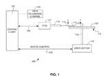
- FIG. 1is a schematic illustration of a disk drive system in which the invention might be embodied
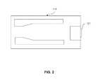
- FIG. 2is an ABS view of a slider illustrating the location of a magnetic head thereon;
- FIGS. 3-6are enlarged ABS views of a magnetoresistive sensor in various intermediate stages of manufacture, illustrating a method for manufacturing a sensor according to the prior art.
- FIGS. 7-17are ABS views of a magnetoresistive sensor in various intermediate stages of manufacture illustrating a method of manufacturing a magnetoresistive sensor according to an alternate embodiment of the invention.
- FIG. 1there is shown a disk drive 100 embodying this invention.
- a disk drive 100embodying this invention.
- at least one rotatable magnetic disk 112is supported on a spindle 114 and rotated by a disk drive motor 118 .
- the magnetic recording on each diskis in the form of annular patterns of concentric data tracks (not shown) on the magnetic disk 112 .
- At least one slider 113is positioned near the magnetic disk 112 , each slider 113 supporting one or more magnetic head assemblies 121 . As the magnetic disk rotates, slider 113 moves radially in and out over the disk surface 122 so that the magnetic head assembly 121 may access different tracks of the magnetic disk where desired data are written.
- Each slider 113is attached to an actuator arm 119 by way of a suspension 115 .
- the suspension 115provides a slight spring force which biases slider 113 against the disk surface 122 .
- Each actuator arm 119is attached to an actuator means 127 .
- the actuator means 127 as shown in FIG. 1may be a voice coil motor (VCM).
- the VCMcomprises a coil movable within a fixed magnetic field, the direction and speed of the coil movements being controlled by the motor current signals supplied by controller 129 .
- the rotation of the magnetic disk 112generates an air bearing between the slider 113 and the disk surface 122 which exerts an upward force or lift on the slider.
- the air bearingthus counter-balances the slight spring force of suspension 115 and supports slider 113 off and slightly above the disk surface by a small, substantially constant spacing during normal operation.
- control unit 129The various components of the disk storage system are controlled in operation by control signals generated by control unit 129 , such as access control signals and internal clock signals.
- control unit 129comprises logic control circuits, storage means and a microprocessor.
- the control unit 129generates control signals to control various system operations such as drive motor control signals on line 123 and head position and seek control signals on line 128 .
- the control signals on line 128provide the desired current profiles to optimally move and position slider 113 to the desired data track on disk 112 .
- Write and read signalsare communicated to and from write and read heads 121 by way of recording channel 125 .
- FIG. 2is an ABS view of the slider 113 , and as can be seen the magnetic head including an inductive write head and a read sensor, is located at a trailing edge of the slider.
- the magnetic head including an inductive write head and a read sensoris located at a trailing edge of the slider.
- FIG. 1The above description of a typical magnetic disk storage system and the accompanying illustration of FIG. 1 are for representation purposes only. It should be apparent that disk storage systems may contain a large number of disks and actuators, and each actuator may support a number of sliders.
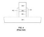
- FIGS. 3-6illustrate a prior art method for manufacturing a magnetoresistive sensor and the associated challenges that arise there from.
- the methodbegins by depositing a series of sensor layers 304 onto a substrate and then depositing a thick CMP stop layer 306 onto the sensor layers.
- a mask 308is formed over the CMP stop layer 306 .
- an ion millingis performed to remove portions of the sensor layers 304 that are not protected by the mask 308 , as shown in FIG. 4 .
- the ion millingalso results in a certain amount of re-deposited material (redep) 402 being formed on the sides of the sensor 304 and CMP stop layer 306 .
- redepre-deposited material
- an insulation layersuch as alumina 501 and hard bias layer 502 are deposited, follow by another thick CMP stop layer 504 , resulting in a structure as shown in FIG. 5 .
- a chemical mechanical polishing (CMP)is performed to remove the mask 308 , and a process such as reactive ion etching is performed to remove the remaining CMP stop layers 306 , 504 .
- An electrically conductive, magnetic shield 602is then formed over the structure as shown in FIG. 6 .
- the process described aboveresults in a large notch 604 being formed at the top of the sensor 304 .
- Thiscauses the shield 602 to have an inconsistent, non-flat shape and results in poor performance and poor control of sensor thickness or “gap”.
- the large amount of re-dep 402remains at the sides of the sensor and is not removed by the chemical mechanical polishing.
- the present inventionaddresses this issue, providing a method for constructing a sensor with a flat shield for excellent gap thickness control and exceptional performance.
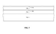
- FIGS. 7-17illustrate a method for manufacturing a sensor according to an embodiment of the invention.
- an electrically conductive, magnetic bottom shield 702is provided. This can be formed on a substrate which is not shown in FIG. 7 .
- a series of magnetoresistive sensor layers 704are deposited over the shield 702 .
- a first layer of material that is resistant to chemical mechanical polishing (CMP stop layer) 706is deposited over the sensor layers 704 .
- One or more masking layersare deposited over the CMP stop layer 706 .
- the masking layerscan include an image transfer layer 708 and a layer of photoresist 710 deposited over the image transfer layer.
- the image transfer layercan be a soluble polymer such as DURIMIDE® or can be some other similar, suitable material.
- Other masking layerssuch as but not limited to one or more hard mask layers, a bottom antireflective coating (BARC) and or a release layer can also be provided in the masking layers, but are not shown in FIG. 7 .
- the sensor layers 704are shown as a whole in FIG. 7 . However, those skilled in the art will appreciate that the sensor layers 704 actually include various magnetic and non-magnetic layers.
- FIG. 17shows the series of sensor layers 704 in greater detail and illustrates a possible arrangement of deposited sensor layers. These sensor layers 704 may include a layer of antiferromagnetic material such as PtMn or IrMn (AFM) 1702 .
- a first magnetic pinned layer AP 1 1704is deposited over the AFM layer 1702
- a thin non-magnetic antiparallel coupling layersuch as Ru 1706 is deposited over the AP 1 layer
- a second magnetic pinned layer 1708is deposited over the antiparallel coupling layer 1706 .
- a non-magnetic spacer or barrier layer 1710is deposited over the AP 2 layer 1708 and a magnetic free layer 1712 is deposited over the non-magnetic layer 1710 .
- the chemical mechanical polishing resistant layer (CMP stop layer) 706is preferably constructed of a high density carbon layer.
- the high density of this carbon layerallows the layer to be thinner than previously used CMP stop layers and thinner than a standard diamond like carbon (DLC) layer.
- the CMP stop layer 706is preferably deposited to a thickness of only 10-15 nm or about 13 nm. This reduced thickness advantageously minimizes upper shield notching, as will become apparent below.
- Carbonwhen formed in a high density, amorphous structure has unique properties. Unlike typical metals or ceramics, it offers better wear resistance and lower coefficient of friction at the same time. A combination of low resistance to wear and low friction is a very attractive attribute as a chemical mechanical polishing (MP) stop layer in that it enables the CMP stop layer 706 to be very thin, while generating less mechanical shear for the areas it is protecting.
- Amorphous carboncan have a density of between 1.5 and 3.3 g/cc and hardness of 10 to 40 GPa. These can be achieved while also having a coefficient of friction that is only 0.1.
- the surface energy of amorphous carboncan be as low as that of TEFLON® with a surface contact angle of 70 to 115 degrees, depending on the process conditions with which it is formed.
- the high density of amorphous carbonalso enables it to protect against chemical penetration of the CMP slurry to prevent chemical attack to the protected structure. All of these properties are favorable to stop Chemical Mechanical Polishing (CMP) both chemically and mechanically where it is not intended while exposing other areas for chemical/mechanical actions for controlled stock removal.
- CMPChemical Mechanical Polishing
- the CMP processis modified to accommodate the reduction in stop layer thickness without resulting in over-polishing.
- the CMP process which needs to be aggressive enough to lift-off the photo-resistis segregated into multiple steps with an aggressive step used for liftoff followed by gentle polishing steps for planarization and cleaning. This breaking up of CMP steps helps prevent over-polishing of the CMP stop layer which protects the sensor and hard bias while resulting in a reduced notch height.
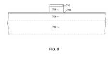
- the photoresist layer 710such as JSR 1891-30N® or some other similar suitable material is photolithographically patterned and developed to form a desired photoresist mask 710 having a shape that is configured to define a magnetoresistive sensor.
- JSR 1891-30Nis non-silicon containing.
- When used to form a stencil consisting of carbon/Durimide/JSR 1891-30Nwould allow RIE slimming to form a narrower trackwidth. RIE etch rates of the individual materials in the stencil are similar, which produces a smooth stencil for ion milling.
- a reactive ion etchingis performed to transfer the image of the photoresist mask onto the underlying image transfer layer 708 and CMP stop layer 706 leaving a structure as that shown in FIG. 9 .
- This reactive ion etchingcan be performed in an oxygen containing chemistry such as O 2 and CO 2 chemistries.
- an ion millingis performed to remove portions of the sensor material 704 that are not protected by the mask layer 708 in order to define a sensor 704 .
- a certain amount of re-deposited material (re-dep) 1002may form on the sides of layer 710 ( FIG. 9 ). Since the re-dep is localized to the side of 710 , a thinner layer 710 minimizes this re-dep.
- the ion millingmay actually include one or more ion millings performed at various angles relative to normal in order to optimize the definition of the side walls, and also to minimize the amount of re-dep 1002 formed on the sides of the sensor 704 .
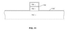
- a thin insulation layer 1102is deposited.
- This insulation layer 1102is preferably alumina (Al 2 O 3 ) and is preferably deposited by a conformal deposition process such as atomic layer deposition (ALD).
- ALDatomic layer deposition
- a layer of hard magnetic material (hard bias layer) 1202is deposited.
- This layer 1202is preferably constructed of a magnetic material having a high magnetic moment such as CoPt or CoPtCr, that is sandwiched between a seed layer consisting of NiTa/CrMo and a cap layer 1204 is deposited over the hard bias layer 1202 .
- the cap layeris preferably a multi-layer structure that includes a layer of material that is resistant to chemical mechanical polishing.
- the cap layer 1204can include a layer of Ta with a layer of Cr thereover (Ta/Cr), a layer of Ta with a layer of Ir thereover (TaIr), or could be Ta/Rh, Ta/Ru, etc.
- Cr, Ir, Rh, Ru, etcare used as CMP stop layer.
- Adding the CMP resistant layere.g. Cr, Ta, Ir, Rh or Ru
- the layer 1202is preferably deposited about to the height of the top of the sensor layer 704 .
- the deposition angle of the seed layer and magnetic materialis desirable between 70-90 degree while the cap optimal angle is between 50-70 degrees.
- An optional second layer of CMP resistant material (2 nd CMP stop layer) 1302may then be deposited over the hard bias layer 1202 as shown in FIG. 13 .
- This second CMP stop layer 1302is also preferably constructed of a high density carbon material, allowing it to be deposited thinner than a conventional diamond like carbon while still providing adequate protection of the hard bias layer 1202 during CMP.
- a chemical mechanical polishingis then performed to remove the mask layer 708 , leaving a structure such as that shown in FIG. 14 .
- This CMPis a multi-step CMP, and includes a more aggressive first CMP step to remove the mask 708 and a second less aggressive gentler CMP to smoothen and clean the structure.
- another reactive ion etchingpreferably performed in a chemistry such as O 2 or CO 2 ) is performed to remove any remaining CMP stop material 706 , 1302 , leaving a structure as shown in FIG. 15 .
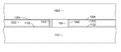
- a second magnetic shield 1602is formed over the sensor layer 704 and hard bias layers 1202 .
- Thiscan be performed by depositing a seed layer, forming an electroplating frame mask, electroplating a magnetic material into an opening in the mask, removing the mask and performing a quick ion milling to remove residual seed material.
- the above described processwhich uses thinner denser CMP stop layers 706 , 1204 ( FIG. 14 ) results in a greatly reduced notch height 1604 and, therefore, results in a much flatter, more uniform shield structure 1602 .
Landscapes
- Engineering & Computer Science (AREA)
- Manufacturing & Machinery (AREA)
- Magnetic Heads (AREA)
- Hall/Mr Elements (AREA)
Abstract
Description
Claims (11)
Priority Applications (1)
| Application Number | Priority Date | Filing Date | Title |
|---|---|---|---|
| US12/645,323US8296930B2 (en) | 2009-12-22 | 2009-12-22 | Method for manufacturing a magnetoresistive sensor having a flat shield |
Applications Claiming Priority (1)
| Application Number | Priority Date | Filing Date | Title |
|---|---|---|---|
| US12/645,323US8296930B2 (en) | 2009-12-22 | 2009-12-22 | Method for manufacturing a magnetoresistive sensor having a flat shield |
Publications (2)
| Publication Number | Publication Date |
|---|---|
| US20110146061A1 US20110146061A1 (en) | 2011-06-23 |
| US8296930B2true US8296930B2 (en) | 2012-10-30 |
Family
ID=44149069
Family Applications (1)
| Application Number | Title | Priority Date | Filing Date |
|---|---|---|---|
| US12/645,323Expired - Fee RelatedUS8296930B2 (en) | 2009-12-22 | 2009-12-22 | Method for manufacturing a magnetoresistive sensor having a flat shield |
Country Status (1)
| Country | Link |
|---|---|
| US (1) | US8296930B2 (en) |
Cited By (5)
| Publication number | Priority date | Publication date | Assignee | Title |
|---|---|---|---|---|
| US20120127616A1 (en)* | 2010-11-24 | 2012-05-24 | Honglin Zhu | Tmr reader without dlc capping structure |
| US20120127615A1 (en)* | 2010-11-24 | 2012-05-24 | Liubo Hong | Tmr reader structure and process for fabrication |
| US20130284693A1 (en)* | 2012-04-27 | 2013-10-31 | Hitachi Global Storage Technologies Netherlands B.V. | Differentiated liftoff process for ultra-shallow mask defined narrow trackwidth magnetic sensor |
| US8614864B1 (en)* | 2008-04-01 | 2013-12-24 | Western Digital (Fremont), Llc | Magnetoresistive device with a hard bias capping layer |
| US8889019B1 (en)* | 2013-05-31 | 2014-11-18 | HGST Netherlands B.V. | Super shallow laminated hard mask stencil for magnetic read sensor fabrication |
Families Citing this family (2)
| Publication number | Priority date | Publication date | Assignee | Title |
|---|---|---|---|---|
| US8771847B2 (en)* | 2011-10-14 | 2014-07-08 | Seagate Technology | Reader stop-layers |
| US8636913B2 (en) | 2011-12-21 | 2014-01-28 | HGST Netherlands B.V. | Removing residues in magnetic head fabrication |
Citations (17)
| Publication number | Priority date | Publication date | Assignee | Title |
|---|---|---|---|---|
| US6723655B2 (en)* | 2001-06-29 | 2004-04-20 | Hynix Semiconductor Inc. | Methods for fabricating a semiconductor device |
| US20060101636A1 (en) | 2004-11-18 | 2006-05-18 | Hitachi Global Storage Technologies | Method for patterning a magnetoresistive sensor |
| US20060136543A1 (en) | 2004-12-21 | 2006-06-22 | Arm Limited | Data processing apparatus and method for performing floating point addition |
| US7094130B2 (en) | 2004-07-30 | 2006-08-22 | Hitachi Global Storage Technologies Netherlands B.V. | Method for fabricating a magnetic transducer using a slurry with spherical particles for CMP-assisted photoresist lift-off |
| US20060231930A1 (en) | 2005-04-19 | 2006-10-19 | Hitachi Global Storage Technologies Netherlands B.V. | Heat resistant photomask for high temperature fabrication processes |
| US20060256482A1 (en) | 2005-05-10 | 2006-11-16 | Hitachi Global Storage Technologies Netherlands, B.V. | Method to fabricate side shields for a magnetic sensor |
| US20060279881A1 (en) | 2005-06-08 | 2006-12-14 | Kiyoshi Sato | Tunneling magnetic sensing element having two-layer insulating film and method for fabricating same |
| US20060292705A1 (en) | 2005-06-24 | 2006-12-28 | Veeco Instruments Inc. | Method and process for fabricating read sensors for read-write heads in mass storage devices |
| US20070081279A1 (en) | 2005-10-06 | 2007-04-12 | Hitachi Global Storage Technologies | Double mill process for patterning current perpendicular to plane (CPP) magnetoresistive devices to minimize barrier shorting and barrier damage |
| US20070230061A1 (en) | 2006-03-28 | 2007-10-04 | Fujitsu Limited | Method for fabricating magnetic head |
| JP2008186543A (en) | 2007-01-31 | 2008-08-14 | Hitachi Global Storage Technologies Netherlands Bv | Magnetoresistive head |
| US7419891B1 (en)* | 2006-02-13 | 2008-09-02 | Western Digital (Fremont), Llc | Method and system for providing a smaller critical dimension magnetic element utilizing a single layer mask |
| US7446981B2 (en) | 2005-08-05 | 2008-11-04 | Hitachi Global Storage Technologies Netherlands B.V. | Magnetic head, fabrication process of magnetic head, and magnetic disk storage apparatus mounting magnetic head |
| US20080274623A1 (en) | 2007-05-02 | 2008-11-06 | Hung-Chin Guthrie | Methods for fabricating a magnetic head reader using a chemical mechanical polishing (cmp) process for sensor stripe height patterning |
| US7522391B2 (en) | 2005-12-14 | 2009-04-21 | Hitachi Global Storage Technologies Netherlands B.V. | Current perpendicular to plane magnetoresistive sensor having a shape enhanced pinned layer and an in stack bias structure |
| US7530158B2 (en) | 2005-04-19 | 2009-05-12 | Hitachi Global Storage Technologies Netherlands B.V. | CPP read sensor fabrication using heat resistant photomask |
| US7536776B2 (en) | 2005-06-14 | 2009-05-26 | Hitachi Global Storage Technologies Netherlands B.V. | Fabrication method for thin film magnetic heads |
- 2009
- 2009-12-22USUS12/645,323patent/US8296930B2/ennot_activeExpired - Fee Related
Patent Citations (18)
| Publication number | Priority date | Publication date | Assignee | Title |
|---|---|---|---|---|
| US6723655B2 (en)* | 2001-06-29 | 2004-04-20 | Hynix Semiconductor Inc. | Methods for fabricating a semiconductor device |
| US7094130B2 (en) | 2004-07-30 | 2006-08-22 | Hitachi Global Storage Technologies Netherlands B.V. | Method for fabricating a magnetic transducer using a slurry with spherical particles for CMP-assisted photoresist lift-off |
| US20060101636A1 (en) | 2004-11-18 | 2006-05-18 | Hitachi Global Storage Technologies | Method for patterning a magnetoresistive sensor |
| US20060136543A1 (en) | 2004-12-21 | 2006-06-22 | Arm Limited | Data processing apparatus and method for performing floating point addition |
| US20060231930A1 (en) | 2005-04-19 | 2006-10-19 | Hitachi Global Storage Technologies Netherlands B.V. | Heat resistant photomask for high temperature fabrication processes |
| US7530158B2 (en) | 2005-04-19 | 2009-05-12 | Hitachi Global Storage Technologies Netherlands B.V. | CPP read sensor fabrication using heat resistant photomask |
| US20060256482A1 (en) | 2005-05-10 | 2006-11-16 | Hitachi Global Storage Technologies Netherlands, B.V. | Method to fabricate side shields for a magnetic sensor |
| US20060279881A1 (en) | 2005-06-08 | 2006-12-14 | Kiyoshi Sato | Tunneling magnetic sensing element having two-layer insulating film and method for fabricating same |
| US7536776B2 (en) | 2005-06-14 | 2009-05-26 | Hitachi Global Storage Technologies Netherlands B.V. | Fabrication method for thin film magnetic heads |
| US20060292705A1 (en) | 2005-06-24 | 2006-12-28 | Veeco Instruments Inc. | Method and process for fabricating read sensors for read-write heads in mass storage devices |
| US7446981B2 (en) | 2005-08-05 | 2008-11-04 | Hitachi Global Storage Technologies Netherlands B.V. | Magnetic head, fabrication process of magnetic head, and magnetic disk storage apparatus mounting magnetic head |
| US20070081279A1 (en) | 2005-10-06 | 2007-04-12 | Hitachi Global Storage Technologies | Double mill process for patterning current perpendicular to plane (CPP) magnetoresistive devices to minimize barrier shorting and barrier damage |
| US7639456B2 (en)* | 2005-10-06 | 2009-12-29 | Hitachi Global Storage Technologies Netherlands B.V. | Double mill process for patterning current perpendicular to plane (CPP) magnetoresistive devices to minimize barrier shorting and barrier damage |
| US7522391B2 (en) | 2005-12-14 | 2009-04-21 | Hitachi Global Storage Technologies Netherlands B.V. | Current perpendicular to plane magnetoresistive sensor having a shape enhanced pinned layer and an in stack bias structure |
| US7419891B1 (en)* | 2006-02-13 | 2008-09-02 | Western Digital (Fremont), Llc | Method and system for providing a smaller critical dimension magnetic element utilizing a single layer mask |
| US20070230061A1 (en) | 2006-03-28 | 2007-10-04 | Fujitsu Limited | Method for fabricating magnetic head |
| JP2008186543A (en) | 2007-01-31 | 2008-08-14 | Hitachi Global Storage Technologies Netherlands Bv | Magnetoresistive head |
| US20080274623A1 (en) | 2007-05-02 | 2008-11-06 | Hung-Chin Guthrie | Methods for fabricating a magnetic head reader using a chemical mechanical polishing (cmp) process for sensor stripe height patterning |
Cited By (9)
| Publication number | Priority date | Publication date | Assignee | Title |
|---|---|---|---|---|
| US8614864B1 (en)* | 2008-04-01 | 2013-12-24 | Western Digital (Fremont), Llc | Magnetoresistive device with a hard bias capping layer |
| US20120127616A1 (en)* | 2010-11-24 | 2012-05-24 | Honglin Zhu | Tmr reader without dlc capping structure |
| US20120127615A1 (en)* | 2010-11-24 | 2012-05-24 | Liubo Hong | Tmr reader structure and process for fabrication |
| US8553370B2 (en)* | 2010-11-24 | 2013-10-08 | HGST Netherlands B.V. | TMR reader structure having shield layer |
| US8553371B2 (en)* | 2010-11-24 | 2013-10-08 | HGST Netherlands B.V. | TMR reader without DLC capping structure |
| US20130284693A1 (en)* | 2012-04-27 | 2013-10-31 | Hitachi Global Storage Technologies Netherlands B.V. | Differentiated liftoff process for ultra-shallow mask defined narrow trackwidth magnetic sensor |
| US8984741B2 (en)* | 2012-04-27 | 2015-03-24 | HGST Netherlands B.V. | Differentiated liftoff process for ultra-shallow mask defined narrow trackwidth magnetic sensor |
| US8889019B1 (en)* | 2013-05-31 | 2014-11-18 | HGST Netherlands B.V. | Super shallow laminated hard mask stencil for magnetic read sensor fabrication |
| US20140353276A1 (en)* | 2013-05-31 | 2014-12-04 | HGST Netherlands B.V. | Super shallow laminated hard mask stencil for magnetic read sensor fabrication |
Also Published As
| Publication number | Publication date |
|---|---|
| US20110146061A1 (en) | 2011-06-23 |
Similar Documents
| Publication | Publication Date | Title |
|---|---|---|
| US8617408B2 (en) | Method for manufacturing a magnetic read sensor with narrow track width using amorphous carbon as a hard mask and localized CMP | |
| US8011084B2 (en) | Method for fabricating narrow magnetic read width TMR/CPP sensors | |
| US7961440B2 (en) | Current perpendicular to plane magnetoresistive sensor with reduced read gap | |
| US8266785B2 (en) | Method for manufacturing a magnetoresistive sensor having a novel junction structure for improved track width definition and pinned layer stability | |
| US7602589B2 (en) | Magnetoresistive sensor having shape enhanced pinning and low lead resistance | |
| US7639456B2 (en) | Double mill process for patterning current perpendicular to plane (CPP) magnetoresistive devices to minimize barrier shorting and barrier damage | |
| US20120156390A1 (en) | Multi-angle hard bias deposition for optimal hard-bias deposition in a magnetic sensor | |
| US7405909B2 (en) | Current perpendicular to plane (CPP) magnetoresistive sensor with free layer biasing by exchange pinning at back edge | |
| US8393073B2 (en) | Method to control mask profile for read sensor definition | |
| US7324310B2 (en) | Self-pinned dual CPP sensor exchange pinned at stripe back-end to avoid amplitude flipping | |
| US8296930B2 (en) | Method for manufacturing a magnetoresistive sensor having a flat shield | |
| US9202482B2 (en) | Magnetic sensor having an extended pinned layer with stitched antiferromagnetic pinning layer | |
| US8137570B2 (en) | Additive write pole process for wrap around shield | |
| US8339753B1 (en) | Magnetic bias structure for magnetoresistive sensor | |
| US20120187079A1 (en) | Method for manufacturing a magnetic sensor having a flat upper shield | |
| US7788798B2 (en) | Method for manufacturing a perpendicular magnetic write head with wrap around magnetic trailing and side shields | |
| US7765676B2 (en) | Method for patterning a magnetoresistive sensor | |
| US7329362B2 (en) | Dual angle milling for current perpendicular to plane (CPP) magnetoresistive sensor definition | |
| US7344330B2 (en) | Topographically defined thin film CPP read head fabrication | |
| US20130083432A1 (en) | Magnetic bias structure for magnetoresistive sensor | |
| US20120125884A1 (en) | Method for manufacturing a narrow magnetic read width current perpendicular to plane magnetoresistive sensor | |
| US9053721B1 (en) | Magnetic read sensor with independently extended pinned layer and seed layer | |
| US8889018B2 (en) | Method for manufacturing a magnetic write pole using a multi-layered hard mask structure | |
| US8037593B2 (en) | Method for manufacturing an ultra narrow gap magnetoresistive sensor | |
| US8615868B2 (en) | Method for manufacturing a magnetic sensor using two step ion milling |
Legal Events
| Date | Code | Title | Description |
|---|---|---|---|
| AS | Assignment | Owner name:HITACHI GLOBAL STORAGE TECHNOLOGIES NETHERLANDS B. Free format text:ASSIGNMENT OF ASSIGNORS INTEREST;ASSIGNORS:FUNADA, SHIN;LE, QUANG;LEONG, THOMAS L.;AND OTHERS;SIGNING DATES FROM 20100111 TO 20100303;REEL/FRAME:024046/0649 | |
| FEPP | Fee payment procedure | Free format text:PAYOR NUMBER ASSIGNED (ORIGINAL EVENT CODE: ASPN); ENTITY STATUS OF PATENT OWNER: LARGE ENTITY | |
| STCF | Information on status: patent grant | Free format text:PATENTED CASE | |
| AS | Assignment | Owner name:HGST, NETHERLANDS B.V., NETHERLANDS Free format text:CHANGE OF NAME;ASSIGNOR:HGST, NETHERLANDS B.V.;REEL/FRAME:029341/0777 Effective date:20120723 Owner name:HGST NETHERLANDS B.V., NETHERLANDS Free format text:CHANGE OF NAME;ASSIGNOR:HITACHI GLOBAL STORAGE TECHNOLOGIES NETHERLANDS B.V.;REEL/FRAME:029341/0777 Effective date:20120723 | |
| CC | Certificate of correction | ||
| FPAY | Fee payment | Year of fee payment:4 | |
| AS | Assignment | Owner name:WESTERN DIGITAL TECHNOLOGIES, INC., CALIFORNIA Free format text:ASSIGNMENT OF ASSIGNORS INTEREST;ASSIGNOR:HGST NETHERLANDS B.V.;REEL/FRAME:040826/0327 Effective date:20160831 | |
| AS | Assignment | Owner name:JPMORGAN CHASE BANK, N.A., AS AGENT, ILLINOIS Free format text:SECURITY INTEREST;ASSIGNOR:WESTERN DIGITAL TECHNOLOGIES, INC.;REEL/FRAME:052915/0566 Effective date:20200113 | |
| FEPP | Fee payment procedure | Free format text:MAINTENANCE FEE REMINDER MAILED (ORIGINAL EVENT CODE: REM.); ENTITY STATUS OF PATENT OWNER: LARGE ENTITY | |
| LAPS | Lapse for failure to pay maintenance fees | Free format text:PATENT EXPIRED FOR FAILURE TO PAY MAINTENANCE FEES (ORIGINAL EVENT CODE: EXP.); ENTITY STATUS OF PATENT OWNER: LARGE ENTITY | |
| STCH | Information on status: patent discontinuation | Free format text:PATENT EXPIRED DUE TO NONPAYMENT OF MAINTENANCE FEES UNDER 37 CFR 1.362 | |
| FP | Lapsed due to failure to pay maintenance fee | Effective date:20201030 | |
| AS | Assignment | Owner name:WESTERN DIGITAL TECHNOLOGIES, INC., CALIFORNIA Free format text:RELEASE OF SECURITY INTEREST AT REEL 052915 FRAME 0566;ASSIGNOR:JPMORGAN CHASE BANK, N.A.;REEL/FRAME:059127/0001 Effective date:20220203 |