US8296508B1 - Secure memory device erase - Google Patents
Secure memory device eraseDownload PDFInfo
- Publication number
- US8296508B1 US8296508B1US12/768,345US76834510AUS8296508B1US 8296508 B1US8296508 B1US 8296508B1US 76834510 AUS76834510 AUS 76834510AUS 8296508 B1US8296508 B1US 8296508B1
- Authority
- US
- United States
- Prior art keywords
- memory device
- memory
- program
- states
- erase command
- Prior art date
- Legal status (The legal status is an assumption and is not a legal conclusion. Google has not performed a legal analysis and makes no representation as to the accuracy of the status listed.)
- Active, expires
Links
Images


Classifications
- G—PHYSICS
- G06—COMPUTING OR CALCULATING; COUNTING
- G06F—ELECTRIC DIGITAL DATA PROCESSING
- G06F21/00—Security arrangements for protecting computers, components thereof, programs or data against unauthorised activity
- G06F21/70—Protecting specific internal or peripheral components, in which the protection of a component leads to protection of the entire computer
- G06F21/78—Protecting specific internal or peripheral components, in which the protection of a component leads to protection of the entire computer to assure secure storage of data
- G06F21/79—Protecting specific internal or peripheral components, in which the protection of a component leads to protection of the entire computer to assure secure storage of data in semiconductor storage media, e.g. directly-addressable memories
- G—PHYSICS
- G11—INFORMATION STORAGE
- G11C—STATIC STORES
- G11C16/00—Erasable programmable read-only memories
- G11C16/02—Erasable programmable read-only memories electrically programmable
- G11C16/06—Auxiliary circuits, e.g. for writing into memory
- G11C16/10—Programming or data input circuits
- G11C16/14—Circuits for erasing electrically, e.g. erase voltage switching circuits
- G—PHYSICS
- G11—INFORMATION STORAGE
- G11C—STATIC STORES
- G11C16/00—Erasable programmable read-only memories
- G11C16/02—Erasable programmable read-only memories electrically programmable
- G11C16/06—Auxiliary circuits, e.g. for writing into memory
- G11C16/22—Safety or protection circuits preventing unauthorised or accidental access to memory cells
- G—PHYSICS
- G06—COMPUTING OR CALCULATING; COUNTING
- G06F—ELECTRIC DIGITAL DATA PROCESSING
- G06F2221/00—Indexing scheme relating to security arrangements for protecting computers, components thereof, programs or data against unauthorised activity
- G06F2221/21—Indexing scheme relating to G06F21/00 and subgroups addressing additional information or applications relating to security arrangements for protecting computers, components thereof, programs or data against unauthorised activity
- G06F2221/2143—Clearing memory, e.g. to prevent the data from being stolen
Definitions
- Subject matter disclosed hereinrelates to an erasable memory device, and more particularly to a securely erasable flash memory device.
- Secrecy and/or privacy issues related to various organizations, such as government, military, financial, or medical organizations, as well as individualsmay be addressed, at least in part, by secure management of data.
- Such data managementmay involve recording, copying, storing, and/or erasing data, for example.
- many erase operationsmay be made on a computing system that does not necessarily physically erase data from memory. Instead, for example, such an erase operation may merely leave “erased” data in particular memory locations while subsequently allowing new data to be written over the “erased” data.
- some erase operationsmay merely be superficial in that higher level computer operations (e.g., user interface) may merely be modified to appear as though memory is erased, even though it may not be.
- FIG. 1is a flow diagram of a process to erase memory, according to an embodiment.
- FIG. 2is a schematic diagram of a memory system, according to an embodiment.
- FIGS. 3-8are state diagrams of memory devices, according to an embodiment.
- FIG. 9is a schematic view of a computing system and a memory device, according to an embodiment.
- a secure erase proceduremay include executing an erase command to erase data on a portion of memory, writing new, random data in the portion of erased memory, and re-execute an erase command.
- an erase proceduremay be slower than desired, involving execution of two erase commands.
- Another problem associated with such an erase procedureis that endurance of a memory device may be reduced, particular if such a memory device comprises flash memory.
- an improved procedure for securely erasing a memory devicemay involve implementing memory states that may only be accessed from within the memory device, as explained in detail below. Such states are herein called hidden states.
- a memory devicemay include memory cells capable of storing data using externally accessible program states, such as 1 or 0, high or low, set or reset, and so on. Such states are herein called externally accessible if such states may be read, programmed, and/or erased from outside the memory device.
- statesmay be accessed from a user interface via an external entity, which may comprise a computer processor, a memory controller, a user interface, and/or other entities external to the memory device.
- a memory devicemay also be capable of storing data using a hidden state that may not be externally accessible from outside the memory device.
- a hidden statemay not be accessed by a user interface and/or an external memory controller.
- a hidden state of a memory devicemay only be implemented from within the memory device.
- a hidden statemay be considered to be an undefined intermediate state that may not be associated with predefined coded states, for example.
- an internal memory management (IMM) portion of a memory devicemay implement processes, operations, and/or functions associated with a hidden state, as described in detail below.
- IMMinternal memory management
- a process managed from within a memory devicemay program memory cells in various initial states to a hidden state, after which a memory erase operation may occur. Such a process may ensure that previous coded states of the memory cells are difficult or impossible to recover after erasing because the process results in an erase state that comes from a hidden state, which may not contain information useable to recover previous states, as discussed below. Moreover, moving such a secure erase procedure to inside a memory device may increase data security.
- FIG. 1is a flow diagram of a process 100 to erase memory, according to an embodiment.
- a memory devicemay store data in the form of memory states that are user-accessible.
- a flash memory devicesuch as a NAND and/or a NOR flash memory device, may include one or more flash memory cells for use in storing a single bit per cell. Such a bit may include one of either a high logic level or a low logic level.
- a flash memory devicemay include one or more multilevel flash memory cells for use in storing multiple bits per cell. Such bits may include one of multiple logic levels.
- a memory cellmay include a transistor having a floating gate located between a control gate and a channel region of the transistor.
- a threshold voltage of such a transistormay be programmed or erased by charging or discharging the floating gate.
- An amount of electrical charge on a floating gate of a transistormay determine which voltage is to be applied to a control gate of the transistor to result in a charge carrier inversion in an underlying channel region.
- An amount of charge on a floating gatetherefore may determine a threshold voltage, and thus a state, of a transistor. Accordingly, data may be written to such memory cells by charging or discharging floating gates of transistors in the memory cells to achieve threshold voltages corresponding to the data.
- a memory controller to implement write and/or a read operationmay be provided to operate such a memory device.
- a memory devicemay receive an erase command initiated by a computer processor, for example, and generated by a memory controller, and/or entity external to the memory device.
- a determinationmay be made as to whether an erase command comprises a secure erase command.
- a determinationmay be made externally with respect to the memory device, such as at a portion of a memory controller.
- a particular signal representing either a secure erase command or a non-secure erase commandmay be provided to the memory device.
- a non-secure eraseis referred to as a “normal erase.”
- such a determinationmay be made internally with respect to the memory device, such as at a management portion and/or internal memory controller located within the memory device.
- an erase command received from outside the memory devicemay be decoded internally to determine whether the received erase command comprises a secure erase command or a normal erase command.
- process 100may proceed to block 140 , where data stored in a memory device may be erased.
- an erase operationmay involve raising a voltage of a substrate of memory cells beyond a particular erase voltage for one or more blocks of memory cells while grounding gates of the memory cells.
- other techniques for erasing memory cellsare possible, and claimed subject matter is not limited to any particular technique.
- process 100may proceed to block 150 , where memory locations where data is stored in a memory device may be programmed to be stored based on a hidden state.
- a hidden statemay only be accessed from within the memory device while not being externally accessible from outside the memory device.
- such a hidden statemay not be accessed by a user interface and/or an external memory controller.
- such a hidden state of a memory devicemay only be implemented from within the memory device. In other words, an operation to program memory locations to a hidden state of a memory device may be generated from only within the memory device.
- Such a hidden statemay be considered to be an undefined intermediate state that may not be associated with predefined coded states, for example.
- a process of programming memory locations storing data in a user-accessible state to a hidden state of a memory cellmay eliminate any record and/or trace of previous states.
- a memory cellmay be transitioned to a hidden state by modifying a gate voltage of the memory cell. After a transition to the hidden state, any previous state may not be determined from the memory cell since physical characteristics of the memory cell are changed from such a previous state.
- a transition to a hidden stateis implemented only from within a memory device, without external action, then there may be no record and/or trace of such a transition to the hidden state outside the memory device. Thus, such a transition to a hidden state may destroy previously stored data, which may be the intention of a secure erase, for example.
- process 100may proceed to block 160 , where data stored in a hidden state in the memory device may be erased and/or reset.
- an erasemay be initiated from within the memory device without action of an external memory controller outside the memory device, for example.
- An erase operationmay involve raising a voltage of a substrate of memory cells beyond a particular erase voltage for one or more blocks of memory cells while grounding gates of the memory cells.
- FIG. 2is a schematic diagram of a memory system 200 , according to an embodiment.
- a memory controller 205which may be responsive to a user interface and/or a computer processor for example, may generate an erase command directed to a memory device 210 .
- Such an erase commandmay comprise a secure erase command or a normal erase command.
- a secure erase commandmay have a setup/confirm command different than that of a normal erase command, for example.
- such a memory controllermay merely generate a normal erase command.
- a memory device 210may treat such a normal erase command as a secure erase command.
- Memory device 210may include a memory array 230 and an internal memory management (IMM) 220 comprising a portion of memory device 210 .
- IMM 220may implement processes, operations, and/or functions associated with one or more hidden states. For example, a particular program-verify process associated with a hidden state in memory array 230 may be implemented by IMM 220 . In detail, such a program-verify process may involve program voltage levels that are higher than program voltage levels associated with externally-accessible states. Also, IMM 220 may implement particular sense amplifier and/or voltage pump parameters associated with one or more hidden states. Additionally, IMM 220 may maintain and/or implement executable code in order to carry out memory operations associated with one or more hidden states.
- IMM 220may receive an erase command from outside memory device 210 , such as from memory controller 205 for example. Upon receiving an erase command, IMM 220 may determine whether the erase command comprises a secure erase command or a normal erase command. Upon such a determination, IMM 220 may implement, for example, portions of process 100 comprising block 150 and/or block 160 , as described above. Of course, such details of memory system 200 are merely examples of possible configurations, and claimed subject matter is not so limited.
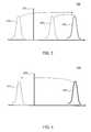
- FIGS. 3-8are state diagrams of memory devices, according to an embodiment.
- a horizontal axisrepresents a relative voltage associated with a memory state while line 301 represents a division between erased states left of line 301 and programmed states right of line 301 .
- positions and/or scales of such an axisare merely examples, and claimed subject matter is not limited in this respect.
- FIG. 3is a state diagram 300 showing an erased or reset state 310 , a programmed or set state 320 , and a hidden state 330 , according to an embodiment.
- states of a memory cellmay be defined by an amount of voltage placed on a gate of the memory cell.
- one or more memory cells in a memory devicemay be in a reset state 310 and/or a set state 320 .
- a memory devicemay store data that may be written over, read, and/or erased, for example.
- a secure erase processsuch as process 100
- memory locations storing data in a memory devicemay be programmed based on a hidden state. Accordingly, both set state 320 and reset state 310 may transition to hidden state 330 , as indicated by arrows in FIG. 3 .
- such programming to hidden state 330may be implemented from within a memory device.
- data stored in hidden state 330may be erased and/or reset to state 410 , as shown in FIG. 4 .
- an erase and/or reset processmay be initiated from within the memory device without action of an external memory controller outside the memory device, for example.
- FIG. 5is a state diagram 500 of a multi-level memory device showing an erased or reset state 510 , programmed or set states 520 , 530 , 540 , and a hidden state 550 , according to an embodiment.
- Such states of a multi-level memory cellmay be defined by an amount of voltage placed on a gate of the memory cell.
- reset state 510 and programmed or set states 520 , 530 , 540may be externally accessible while hidden state 550 may only be accessed and/or implemented from within the memory device, as discussed above.
- a secure erase processsuch as process 100 , may be carried out.
- memory locations storing data in a memory devicemay be programmed based on a hidden state. Accordingly, set states 520 , 530 , and 540 and reset state 510 may transition to hidden state 550 , as indicated by arrows in FIG. 5 . Again, such programming to hidden state 550 may be implemented from within a memory device.
- data stored in hidden state 550may be erased and/or reset to state 610 , as shown in FIG. 6 . Again, such an erase and/or reset process may be initiated from within the memory device without action of an external memory controller outside the memory device, for example.
- FIG. 6such details of hidden states and state transitions are merely examples, and claimed subject matter is not so limited.
- FIG. 7is a state diagram 700 of a single-level memory device showing an erased or reset state 720 and a programmed or set state 750 , according to an embodiment.
- Such states of a single-level memory cellmay be defined by an amount of voltage placed on a gate of the memory cell.
- one or more hidden statesmay be internally implemented.
- hidden states 710 , 730 , 740 , and 750may comprise hidden states that are not externally accessed.
- Such hidden statesmay be distributed across a relatively wide range of state voltages.
- hidden states 710 and 730may involve state voltages relatively close to that of reset state 720 .
- hidden states 740 and 760may involve state voltages relatively close to that of set state 750 .
- FIG. 8is a state diagram 800 of a multi-level memory device showing an erased or reset state 810 and programmed or set states 830 , 845 , and 855 , according to an embodiment.
- states of a multi-level memory cellmay be defined by an amount of voltage placed on a gate of the memory cell.
- one or more hidden statesmay be internally implemented.
- hidden states 805 , 815 , 825 , 835 , 850 , and 860may comprise hidden states that may not be externally accessed.
- Such hidden statesmay be distributed across a relatively wide range of state voltages.
- hidden states 805 and 815may involve state voltages relatively close to that of reset state 810 .
- hidden states 825 , 835 , and 850may involve state voltages relatively close to that of set states 830 , 845 , and 855 .
- FIG. 9is a schematic diagram illustrating an exemplary embodiment of a computing system 900 including a memory device 910 .
- a computing devicemay comprise one or more processors, for example, to execute an application and/or other code.
- memory device 910may comprise a memory array 230 shown in FIG. 1 .
- a computing device 904may be representative of any device, appliance, or machine that may be configurable to manage memory device 910 .
- Memory device 910may include a memory controller 915 and a memory 922 .
- computing device 904may include: one or more computing devices and/or platforms, such as, e.g., a desktop computer, a laptop computer, a workstation, a server device, or the like; one or more personal computing or communication devices or appliances, such as, e.g., a personal digital assistant, mobile communication device, or the like; a computing system and/or associated service provider capability, such as, e.g., a database or data storage service provider/system; and/or any combination thereof.
- computing devices and/or platformssuch as, e.g., a desktop computer, a laptop computer, a workstation, a server device, or the like
- personal computing or communication devices or appliancessuch as, e.g., a personal digital assistant, mobile communication device, or the like
- a computing system and/or associated service provider capabilitysuch as, e.g., a database or data storage service provider/system; and/or any combination thereof.
- computing device 904may include at least one processing unit 920 that is operatively coupled to memory 922 through a bus 940 and a host or memory controller 915 .
- Processing unit 920is representative of one or more circuits configurable to perform at least a portion of a data computing procedure or process.
- processing unit 920may include one or more processors, controllers, microprocessors, microcontrollers, application specific integrated circuits, digital signal processors, programmable logic devices, field programmable gate arrays, and the like, or any combination thereof.
- Processing unit 920may include an operating system configured to communicate with memory controller 915 .
- Such an operating systemmay, for example, generate commands to be sent to memory controller 915 over bus 940 .
- Such commandsmay comprise read and/or write commands.
- memory controller 915may provide a bias signal, such as a set or reset pulse to write information associated with the write command to a memory partition, for example.
- memory controller 915may provide erase commands to a memory device that includes an IMM portion to store data in the memory device using two or more program states that are accessible by the memory controller.
- Such an IMMmay also program memory locations storing data in a hidden state that is defined internally to the memory device in response to receiving an erase command from the memory controller.
- Memory 922is representative of any data storage mechanism.
- Memory 922may include, for example, a primary memory 924 and/or a secondary memory 926 , each of which may be partitioned into one or more partitions as discussed above, for example.
- Primary memory 924may include, for example, a random access memory, read only memory, etc. While illustrated in this example as being separate from processing unit 920 , it should be understood that all or part of primary memory 924 may be provided within or otherwise co-located/coupled with processing unit 920 .
- Secondary memory 926may include, for example, the same or similar type of memory as primary memory and/or one or more data storage devices or systems, such as, for example, a disk drive, an optical disc drive, a tape drive, a solid state memory drive, etc.
- secondary memory 926may be operatively receptive of, or otherwise configurable to couple to, a computer-readable medium 928 .
- Computer-readable medium 928may include, for example, any medium that can carry and/or make accessible data, code, and/or instructions for one or more of the devices in system 900 .
- Computing device 904may include, for example, an input/output 932 .
- Input/output 932is representative of one or more devices or features that may be configurable to accept or otherwise introduce human and/or machine inputs, and/or one or more devices or features that may be configurable to deliver or otherwise provide for human and/or machine outputs.
- input/output device 932may include an operatively configured display, speaker, keyboard, mouse, trackball, touch screen, data port, etc.
Landscapes
- Engineering & Computer Science (AREA)
- Computer Security & Cryptography (AREA)
- Computer Hardware Design (AREA)
- Theoretical Computer Science (AREA)
- Software Systems (AREA)
- Physics & Mathematics (AREA)
- General Engineering & Computer Science (AREA)
- General Physics & Mathematics (AREA)
- Read Only Memory (AREA)
Abstract
Description
Claims (17)
Priority Applications (1)
| Application Number | Priority Date | Filing Date | Title |
|---|---|---|---|
| US12/768,345US8296508B1 (en) | 2010-04-27 | 2010-04-27 | Secure memory device erase |
Applications Claiming Priority (1)
| Application Number | Priority Date | Filing Date | Title |
|---|---|---|---|
| US12/768,345US8296508B1 (en) | 2010-04-27 | 2010-04-27 | Secure memory device erase |
Publications (1)
| Publication Number | Publication Date |
|---|---|
| US8296508B1true US8296508B1 (en) | 2012-10-23 |
Family
ID=47017545
Family Applications (1)
| Application Number | Title | Priority Date | Filing Date |
|---|---|---|---|
| US12/768,345Active2030-11-18US8296508B1 (en) | 2010-04-27 | 2010-04-27 | Secure memory device erase |
Country Status (1)
| Country | Link |
|---|---|
| US (1) | US8296508B1 (en) |
Cited By (6)
| Publication number | Priority date | Publication date | Assignee | Title |
|---|---|---|---|---|
| US20140122922A1 (en)* | 2012-10-26 | 2014-05-01 | Lsi Corporation | Methods and structure to assure data integrity in a storage device cache in the presence of intermittent failures of cache memory subsystem |
| US9032264B2 (en) | 2013-03-21 | 2015-05-12 | Kabushiki Kaisha Toshiba | Test method for nonvolatile memory |
| US20150149740A1 (en)* | 2013-11-22 | 2015-05-28 | SK Hynix Inc. | Data storage device and data processing system including the same |
| US20160034217A1 (en)* | 2014-07-31 | 2016-02-04 | Samsung Electronics Co., Ltd. | Memory controller configured to control data sanitization and memory system including the same |
| KR20180004874A (en)* | 2016-07-04 | 2018-01-15 | 삼성전자주식회사 | Operation method of nonvolatile memory system and operation method of nonvolatile memory device |
| US11348650B2 (en)* | 2020-07-14 | 2022-05-31 | Micron Technology, Inc. | Destruction of data and verification of data destruction on a memory device |
Citations (11)
| Publication number | Priority date | Publication date | Assignee | Title |
|---|---|---|---|---|
| US6961829B2 (en)* | 2001-06-06 | 2005-11-01 | Koninklijke Philips Electronics N.V. | Data carrier comprising memory means for storing information significant for intermediate operating states |
| US20060266250A1 (en)* | 2005-05-25 | 2006-11-30 | Microsoft Corporation | Methods and apparatus enabling diagram customization retention |
| US20070150891A1 (en)* | 2005-12-22 | 2007-06-28 | Shapiro Alan J | Method and apparatus for dispensing on a data-storage medium customized content comprising selected assets |
| US20070245109A1 (en)* | 2006-04-07 | 2007-10-18 | Stmicroelectronics Sa | Method for securing data blocks in an electrically programmable memory |
| US20080209106A1 (en)* | 2004-07-21 | 2008-08-28 | Stmicroelectronics Limited | Memory access |
| US20080219057A1 (en)* | 2007-03-07 | 2008-09-11 | Yan Li | Non-Volatile Memory With Cache Page Copy |
| US20090132760A1 (en)* | 2006-12-06 | 2009-05-21 | David Flynn | Apparatus, system, and method for solid-state storage as cache for high-capacity, non-volatile storage |
| US20100082962A1 (en)* | 2008-10-01 | 2010-04-01 | Novell, Inc. | Flash memory device for booting a computing device including embedded general purpose operating system |
| US20100082885A1 (en)* | 2008-09-28 | 2010-04-01 | Ramot At Tel Aviv University Ltd. | Method and system for adaptive coding in flash memories |
| US20110044102A1 (en)* | 2009-08-19 | 2011-02-24 | Yingda Dong | Selective memory cell program and erase |
| US20110283081A1 (en)* | 2010-05-13 | 2011-11-17 | Gerald Barkley | Staggered programming for resistive memories |
- 2010
- 2010-04-27USUS12/768,345patent/US8296508B1/enactiveActive
Patent Citations (13)
| Publication number | Priority date | Publication date | Assignee | Title |
|---|---|---|---|---|
| US6961829B2 (en)* | 2001-06-06 | 2005-11-01 | Koninklijke Philips Electronics N.V. | Data carrier comprising memory means for storing information significant for intermediate operating states |
| US20080209106A1 (en)* | 2004-07-21 | 2008-08-28 | Stmicroelectronics Limited | Memory access |
| US20060266250A1 (en)* | 2005-05-25 | 2006-11-30 | Microsoft Corporation | Methods and apparatus enabling diagram customization retention |
| US20070150891A1 (en)* | 2005-12-22 | 2007-06-28 | Shapiro Alan J | Method and apparatus for dispensing on a data-storage medium customized content comprising selected assets |
| US20080141242A1 (en)* | 2005-12-22 | 2008-06-12 | Alan Joshua Shapiro | Method and apparatus for delivering percepta |
| US20070245109A1 (en)* | 2006-04-07 | 2007-10-18 | Stmicroelectronics Sa | Method for securing data blocks in an electrically programmable memory |
| US20110289267A1 (en)* | 2006-12-06 | 2011-11-24 | Fusion-Io, Inc. | Apparatus, system, and method for solid-state storage as cache for high-capacity, non-volatile storage |
| US20090132760A1 (en)* | 2006-12-06 | 2009-05-21 | David Flynn | Apparatus, system, and method for solid-state storage as cache for high-capacity, non-volatile storage |
| US20080219057A1 (en)* | 2007-03-07 | 2008-09-11 | Yan Li | Non-Volatile Memory With Cache Page Copy |
| US20100082885A1 (en)* | 2008-09-28 | 2010-04-01 | Ramot At Tel Aviv University Ltd. | Method and system for adaptive coding in flash memories |
| US20100082962A1 (en)* | 2008-10-01 | 2010-04-01 | Novell, Inc. | Flash memory device for booting a computing device including embedded general purpose operating system |
| US20110044102A1 (en)* | 2009-08-19 | 2011-02-24 | Yingda Dong | Selective memory cell program and erase |
| US20110283081A1 (en)* | 2010-05-13 | 2011-11-17 | Gerald Barkley | Staggered programming for resistive memories |
Cited By (9)
| Publication number | Priority date | Publication date | Assignee | Title |
|---|---|---|---|---|
| US20140122922A1 (en)* | 2012-10-26 | 2014-05-01 | Lsi Corporation | Methods and structure to assure data integrity in a storage device cache in the presence of intermittent failures of cache memory subsystem |
| US8874973B2 (en)* | 2012-10-26 | 2014-10-28 | Lsi Corporation | Methods and structure to assure data integrity in a storage device cache in the presence of intermittent failures of cache memory subsystem |
| US9032264B2 (en) | 2013-03-21 | 2015-05-12 | Kabushiki Kaisha Toshiba | Test method for nonvolatile memory |
| US20150149740A1 (en)* | 2013-11-22 | 2015-05-28 | SK Hynix Inc. | Data storage device and data processing system including the same |
| US20160034217A1 (en)* | 2014-07-31 | 2016-02-04 | Samsung Electronics Co., Ltd. | Memory controller configured to control data sanitization and memory system including the same |
| KR20180004874A (en)* | 2016-07-04 | 2018-01-15 | 삼성전자주식회사 | Operation method of nonvolatile memory system and operation method of nonvolatile memory device |
| US11348650B2 (en)* | 2020-07-14 | 2022-05-31 | Micron Technology, Inc. | Destruction of data and verification of data destruction on a memory device |
| US20220246222A1 (en)* | 2020-07-14 | 2022-08-04 | Micron Technology, Inc. | Destruction of data and verification of data destruction on a memory device |
| US11749362B2 (en)* | 2020-07-14 | 2023-09-05 | Micron Technology, Inc. | Destruction of data and verification of data destruction on a memory device |
Similar Documents
| Publication | Publication Date | Title |
|---|---|---|
| CN110400588B (en) | Memory device and operating method thereof | |
| KR102226367B1 (en) | Nonvolatile memory device and nonvolatile memory system including the same | |
| US8451662B2 (en) | Reading memory cell history during program operation for adaptive programming | |
| KR102520540B1 (en) | Memory device and operating method thereof | |
| US10437518B2 (en) | Memory system and method of operating the same | |
| US8296508B1 (en) | Secure memory device erase | |
| KR102163872B1 (en) | Multi-bit memory device, onchip buffered program method thereof and multi-bit memory system | |
| KR102154499B1 (en) | Nonvolatile memory device and driving method of the same | |
| US9941016B2 (en) | Flash memory device performing adaptive loop, memory system and method of operating the memory system | |
| US9842653B2 (en) | Semiconductor memory device and operating method of biasing memory blocks | |
| KR102424372B1 (en) | Memory device and operating method thereof | |
| KR20190087845A (en) | Memory system and operating method thereof | |
| KR20120056113A (en) | Nonvolatile meomory device and program method thereof, memory system comprising the same | |
| KR102565913B1 (en) | Memory system having storage device and memory controller and operating method thereof | |
| US9159383B2 (en) | Signal management in a memory device | |
| US20200176065A1 (en) | Memory controller, memory system including memory controller, method of operating memory controller | |
| KR20120049509A (en) | Row decoder circuit and non-volatile memory device including the same | |
| KR20190084518A (en) | Memory system and operating method thereof | |
| US11127475B2 (en) | Memory device controlling operating voltage of select transistor and method of operating the same | |
| CN114527933A (en) | Memory operation method, memory and memory system | |
| KR20230045334A (en) | Memory device and operating method thereof | |
| KR20240069949A (en) | Memory, storage device and method for operating thereof improving performance of read retry operation | |
| KR102461751B1 (en) | Memory device and operating method thereof | |
| KR102774171B1 (en) | Memory device and operating method thereof | |
| KR20100098968A (en) | Nonvolatile memory device, programming method thereof and memory system including the same |
Legal Events
| Date | Code | Title | Description |
|---|---|---|---|
| AS | Assignment | Owner name:NUMONYX B.V., SWITZERLAND Free format text:ASSIGNMENT OF ASSIGNORS INTEREST;ASSIGNORS:ZANARDI, STEFANO;GUERRA, GIOVANNI;MONTELEONE, DOMENICO;AND OTHERS;SIGNING DATES FROM 20100401 TO 20100424;REEL/FRAME:024763/0512 | |
| AS | Assignment | Owner name:MICRON TECHNOLOGY, INC., IDAHO Free format text:ASSIGNMENT OF ASSIGNORS INTEREST;ASSIGNOR:NUMONYX B.V.;REEL/FRAME:027126/0176 Effective date:20110930 | |
| FEPP | Fee payment procedure | Free format text:PAYOR NUMBER ASSIGNED (ORIGINAL EVENT CODE: ASPN); ENTITY STATUS OF PATENT OWNER: LARGE ENTITY | |
| STCF | Information on status: patent grant | Free format text:PATENTED CASE | |
| FPAY | Fee payment | Year of fee payment:4 | |
| AS | Assignment | Owner name:U.S. BANK NATIONAL ASSOCIATION, AS COLLATERAL AGENT, CALIFORNIA Free format text:SECURITY INTEREST;ASSIGNOR:MICRON TECHNOLOGY, INC.;REEL/FRAME:038669/0001 Effective date:20160426 Owner name:U.S. BANK NATIONAL ASSOCIATION, AS COLLATERAL AGEN Free format text:SECURITY INTEREST;ASSIGNOR:MICRON TECHNOLOGY, INC.;REEL/FRAME:038669/0001 Effective date:20160426 | |
| AS | Assignment | Owner name:MORGAN STANLEY SENIOR FUNDING, INC., AS COLLATERAL AGENT, MARYLAND Free format text:PATENT SECURITY AGREEMENT;ASSIGNOR:MICRON TECHNOLOGY, INC.;REEL/FRAME:038954/0001 Effective date:20160426 Owner name:MORGAN STANLEY SENIOR FUNDING, INC., AS COLLATERAL Free format text:PATENT SECURITY AGREEMENT;ASSIGNOR:MICRON TECHNOLOGY, INC.;REEL/FRAME:038954/0001 Effective date:20160426 | |
| AS | Assignment | Owner name:U.S. BANK NATIONAL ASSOCIATION, AS COLLATERAL AGENT, CALIFORNIA Free format text:CORRECTIVE ASSIGNMENT TO CORRECT THE REPLACE ERRONEOUSLY FILED PATENT #7358718 WITH THE CORRECT PATENT #7358178 PREVIOUSLY RECORDED ON REEL 038669 FRAME 0001. ASSIGNOR(S) HEREBY CONFIRMS THE SECURITY INTEREST;ASSIGNOR:MICRON TECHNOLOGY, INC.;REEL/FRAME:043079/0001 Effective date:20160426 Owner name:U.S. BANK NATIONAL ASSOCIATION, AS COLLATERAL AGEN Free format text:CORRECTIVE ASSIGNMENT TO CORRECT THE REPLACE ERRONEOUSLY FILED PATENT #7358718 WITH THE CORRECT PATENT #7358178 PREVIOUSLY RECORDED ON REEL 038669 FRAME 0001. ASSIGNOR(S) HEREBY CONFIRMS THE SECURITY INTEREST;ASSIGNOR:MICRON TECHNOLOGY, INC.;REEL/FRAME:043079/0001 Effective date:20160426 | |
| AS | Assignment | Owner name:JPMORGAN CHASE BANK, N.A., AS COLLATERAL AGENT, ILLINOIS Free format text:SECURITY INTEREST;ASSIGNORS:MICRON TECHNOLOGY, INC.;MICRON SEMICONDUCTOR PRODUCTS, INC.;REEL/FRAME:047540/0001 Effective date:20180703 Owner name:JPMORGAN CHASE BANK, N.A., AS COLLATERAL AGENT, IL Free format text:SECURITY INTEREST;ASSIGNORS:MICRON TECHNOLOGY, INC.;MICRON SEMICONDUCTOR PRODUCTS, INC.;REEL/FRAME:047540/0001 Effective date:20180703 | |
| AS | Assignment | Owner name:MICRON TECHNOLOGY, INC., IDAHO Free format text:RELEASE BY SECURED PARTY;ASSIGNOR:U.S. BANK NATIONAL ASSOCIATION, AS COLLATERAL AGENT;REEL/FRAME:047243/0001 Effective date:20180629 | |
| AS | Assignment | Owner name:MICRON TECHNOLOGY, INC., IDAHO Free format text:RELEASE BY SECURED PARTY;ASSIGNOR:MORGAN STANLEY SENIOR FUNDING, INC., AS COLLATERAL AGENT;REEL/FRAME:050937/0001 Effective date:20190731 | |
| AS | Assignment | Owner name:MICRON SEMICONDUCTOR PRODUCTS, INC., IDAHO Free format text:RELEASE BY SECURED PARTY;ASSIGNOR:JPMORGAN CHASE BANK, N.A., AS COLLATERAL AGENT;REEL/FRAME:051028/0001 Effective date:20190731 Owner name:MICRON TECHNOLOGY, INC., IDAHO Free format text:RELEASE BY SECURED PARTY;ASSIGNOR:JPMORGAN CHASE BANK, N.A., AS COLLATERAL AGENT;REEL/FRAME:051028/0001 Effective date:20190731 | |
| MAFP | Maintenance fee payment | Free format text:PAYMENT OF MAINTENANCE FEE, 8TH YEAR, LARGE ENTITY (ORIGINAL EVENT CODE: M1552); ENTITY STATUS OF PATENT OWNER: LARGE ENTITY Year of fee payment:8 | |
| MAFP | Maintenance fee payment | Free format text:PAYMENT OF MAINTENANCE FEE, 12TH YEAR, LARGE ENTITY (ORIGINAL EVENT CODE: M1553); ENTITY STATUS OF PATENT OWNER: LARGE ENTITY Year of fee payment:12 |