US8295078B2 - Semiconductor memory cell and array using punch-through to program and read same - Google Patents
Semiconductor memory cell and array using punch-through to program and read sameDownload PDFInfo
- Publication number
- US8295078B2 US8295078B2US13/092,704US201113092704AUS8295078B2US 8295078 B2US8295078 B2US 8295078B2US 201113092704 AUS201113092704 AUS 201113092704AUS 8295078 B2US8295078 B2US 8295078B2
- Authority
- US
- United States
- Prior art keywords
- voltage potential
- memory cell
- potential applied
- transistor
- region
- Prior art date
- Legal status (The legal status is an assumption and is not a legal conclusion. Google has not performed a legal analysis and makes no representation as to the accuracy of the status listed.)
- Active
Links
- 239000004065semiconductorSubstances0.000titleclaimsdescription32
- 210000000746body regionAnatomy0.000claimsabstractdescription82
- 239000000758substrateSubstances0.000claimsabstractdescription29
- 239000012212insulatorSubstances0.000claimsabstractdescription19
- 230000004044responseEffects0.000claimsabstractdescription14
- 238000000034methodMethods0.000claimsdescription69
- 238000007667floatingMethods0.000claimsdescription37
- 239000000463materialSubstances0.000description20
- 239000000969carrierSubstances0.000description14
- 238000005516engineering processMethods0.000description9
- 239000012535impuritySubstances0.000description6
- 238000009413insulationMethods0.000description5
- 230000002093peripheral effectEffects0.000description5
- VYPSYNLAJGMNEJ-UHFFFAOYSA-NSilicium dioxideChemical compoundO=[Si]=OVYPSYNLAJGMNEJ-UHFFFAOYSA-N0.000description4
- 238000003491arrayMethods0.000description4
- 230000003247decreasing effectEffects0.000description4
- 238000004519manufacturing processMethods0.000description4
- 239000007943implantSubstances0.000description3
- 230000014759maintenance of locationEffects0.000description3
- XUIMIQQOPSSXEZ-UHFFFAOYSA-NSiliconChemical compound[Si]XUIMIQQOPSSXEZ-UHFFFAOYSA-N0.000description2
- 239000002800charge carrierSubstances0.000description2
- 229910052732germaniumInorganic materials0.000description2
- GNPVGFCGXDBREM-UHFFFAOYSA-Ngermanium atomChemical compound[Ge]GNPVGFCGXDBREM-UHFFFAOYSA-N0.000description2
- 238000005086pumpingMethods0.000description2
- 238000005070samplingMethods0.000description2
- 229910052710siliconInorganic materials0.000description2
- 239000010703siliconSubstances0.000description2
- 235000012239silicon dioxideNutrition0.000description2
- 239000000377silicon dioxideSubstances0.000description2
- 230000002123temporal effectEffects0.000description2
- JBRZTFJDHDCESZ-UHFFFAOYSA-NAsGaChemical compound[As]#[Ga]JBRZTFJDHDCESZ-UHFFFAOYSA-N0.000description1
- 229910001218Gallium arsenideInorganic materials0.000description1
- 238000009825accumulationMethods0.000description1
- 230000000903blocking effectEffects0.000description1
- 239000013590bulk materialSubstances0.000description1
- 230000015556catabolic processEffects0.000description1
- 230000006378damageEffects0.000description1
- 238000006731degradation reactionMethods0.000description1
- 230000001627detrimental effectEffects0.000description1
- 238000010586diagramMethods0.000description1
- 230000000694effectsEffects0.000description1
- 239000011159matrix materialSubstances0.000description1
- 238000012986modificationMethods0.000description1
- 230000004048modificationEffects0.000description1
- 230000005641tunnelingEffects0.000description1
Images


Classifications
- G—PHYSICS
- G11—INFORMATION STORAGE
- G11C—STATIC STORES
- G11C11/00—Digital stores characterised by the use of particular electric or magnetic storage elements; Storage elements therefor
- G11C11/21—Digital stores characterised by the use of particular electric or magnetic storage elements; Storage elements therefor using electric elements
- G11C11/34—Digital stores characterised by the use of particular electric or magnetic storage elements; Storage elements therefor using electric elements using semiconductor devices
- G11C11/40—Digital stores characterised by the use of particular electric or magnetic storage elements; Storage elements therefor using electric elements using semiconductor devices using transistors
- G11C11/401—Digital stores characterised by the use of particular electric or magnetic storage elements; Storage elements therefor using electric elements using semiconductor devices using transistors forming cells needing refreshing or charge regeneration, i.e. dynamic cells
- G11C11/403—Digital stores characterised by the use of particular electric or magnetic storage elements; Storage elements therefor using electric elements using semiconductor devices using transistors forming cells needing refreshing or charge regeneration, i.e. dynamic cells with charge regeneration common to a multiplicity of memory cells, i.e. external refresh
- G11C11/404—Digital stores characterised by the use of particular electric or magnetic storage elements; Storage elements therefor using electric elements using semiconductor devices using transistors forming cells needing refreshing or charge regeneration, i.e. dynamic cells with charge regeneration common to a multiplicity of memory cells, i.e. external refresh with one charge-transfer gate, e.g. MOS transistor, per cell
- H—ELECTRICITY
- H10—SEMICONDUCTOR DEVICES; ELECTRIC SOLID-STATE DEVICES NOT OTHERWISE PROVIDED FOR
- H10B—ELECTRONIC MEMORY DEVICES
- H10B12/00—Dynamic random access memory [DRAM] devices
- H—ELECTRICITY
- H10—SEMICONDUCTOR DEVICES; ELECTRIC SOLID-STATE DEVICES NOT OTHERWISE PROVIDED FOR
- H10B—ELECTRONIC MEMORY DEVICES
- H10B12/00—Dynamic random access memory [DRAM] devices
- H10B12/20—DRAM devices comprising floating-body transistors, e.g. floating-body cells
- H—ELECTRICITY
- H10—SEMICONDUCTOR DEVICES; ELECTRIC SOLID-STATE DEVICES NOT OTHERWISE PROVIDED FOR
- H10D—INORGANIC ELECTRIC SEMICONDUCTOR DEVICES
- H10D30/00—Field-effect transistors [FET]
- H10D30/60—Insulated-gate field-effect transistors [IGFET]
- H10D30/711—Insulated-gate field-effect transistors [IGFET] having floating bodies
- G—PHYSICS
- G11—INFORMATION STORAGE
- G11C—STATIC STORES
- G11C2211/00—Indexing scheme relating to digital stores characterized by the use of particular electric or magnetic storage elements; Storage elements therefor
- G11C2211/401—Indexing scheme relating to cells needing refreshing or charge regeneration, i.e. dynamic cells
- G11C2211/4016—Memory devices with silicon-on-insulator cells
Definitions
- DRAMsemiconductor dynamic random access memory
- the memory cellmay consist of a PD or a FD SOI transistor (or transistor formed in bulk material/substrate) having a channel, which is disposed adjacent to the body and separated therefrom by a gate dielectric.
- the body region of the transistoris electrically floating in view of the insulation or non-conductive region (for example, in bulk-type material/substrate) disposed beneath the body region.
- the state of memory cellis determined by the concentration of charge in the body region of the transistor.
- semiconductor DRAM array 10includes a plurality of memory cells 12 , each consisting of transistor 14 having gate 16 , an electrically floating body region 18 , source region 20 and drain region 22 .
- the body region 18is disposed between source region 20 and drain region 22 .
- body region 18is disposed on or above region 24 , which may be an insulation region (for example, in SOI material/substrate) or non-conductive region (for example, in bulk-type material/substrate).
- the insulation or non-conductive regionmay be disposed on substrate 26 .
- Datais written into or read from a selected memory cell by applying suitable control signals to a selected word line(s) 28 , a selected source line(s) 30 and/or a selected bit line(s) 32 .
- charge carriersare accumulated in or emitted and/or ejected from electrically floating body region 18 wherein the data states are defined by the amount of carriers within electrically floating body region 18 .
- the entire contents of the Semiconductor Memory Device Patent Applicationincluding, for example, the features, attributes, architectures, configurations, materials, techniques and advantages described and illustrated therein, are incorporated by reference herein.
- logic high or State “1”corresponds to an increased concentration of majority carriers in the body region relative to an unprogrammed device and/or a device that is programmed with a logic low or State “0”.
- a logic low or State “0”corresponds to a reduced concentration of majority carriers in the body region relative to an unprogrammed device and/or a device that is programmed with logic high or State “1”.
- the present inventionsare directed to an integrated circuit device (for example, logic or discrete memory device) comprising a memory cell including at least one transistor, wherein the transistor, in operation, operates in a punch-through.
- the transistorincludes (i) a first region having impurities to provide a first conductivity type and a first junction, (ii) a second region having impurities to provide a first conductivity type and a second junction, wherein when the transistor is in operation, the first and second junctions abut or overlap, (iii) a body region, disposed between the first region and the second region, having impurities to provide a second conductivity type wherein the second conductivity type is different from the first conductivity type.
- the transistorfurther includes (i) a gate disposed over the body region and (ii) a gate insulator disposed between the gate and the body region wherein the body region includes a storage node which is located, at least in part, immediately beneath the gate insulator.
- the memory cellincludes at least two data states which are representative of a charge in the body region.
- the integrated circuit devicefurther includes first circuitry, coupled to the transistor of the memory cell, to: (1) generate first and second sets of write control signals and (2a) apply the first set of write control signals to the transistor to write a first data state in the memory cell and (2b) apply the second set of write control signals to the transistor to write a second data state in the memory cell.
- the transistorprovides at least a first charge (for example, substantially in the storage node of the body region) which is representative of the first data state in the body region via impact ionization.
- the body region of the transistoris electrically floating.
- the transistoris disposed in or on a semiconductor region or layer which resides on or above an insulating region or layer of a substrate wherein the body region is disposed between the first region, the second region, the gate insulator and the insulating region or layer of the substrate.
- the transistormay be disposed on bulk-type semiconductor substrate or SOI-type substrate.
- the transistorin response to read control signals applied to the memory cell, generates a punch-through current which is representative of the data state of the memory cell and wherein the data sense circuitry determines the data state of the memory cell at least substantially based on the second bipolar transistor current.
- the integrated circuit devicemay further include second circuitry to read the data state of the memory cell wherein second circuitry determines the data state of the memory cell at least substantially based on a punch-through current.
- the present inventionsare directed to an integrated circuit device (for example, logic or discrete memory device) comprising a memory cell including at least one punch-through mode transistor, wherein the punch-through mode transistor includes: (i) a first region, (ii) a second region, (iii) a body region disposed between the first region and the second region, (iv) a gate disposed over the body region and (v) a gate insulator disposed between the gate and the body region wherein the body region includes a storage node which is located, at least in part, immediately beneath the gate insulator.
- the memory cellincludes at least two data states including (i) a first data state which is representative of a first charge in the body region, and (ii) a second data state which is representative of a second charge in the body region.
- the integrated circuit device of this aspectmay include first circuitry, coupled to the transistor of the memory cell, to: (1) generate first and second sets of write control signals and (2a) apply the first set of write control signals to the transistor to write the first data state in the memory cell and (2b) apply the second set of write control signals to the transistor to write the second data state in the memory cell.
- the transistorin response to the first set of write control signals, stores at least the first charge in the body region (for example, substantially in the storage node) wherein the first charge is provided or created via impact ionization and, in response to the second set of write control signals, the transistor stores no more than the second charge in the body region.
- the body region of the transistoris electrically floating.
- the transistoris disposed in or on a semiconductor region or layer which resides on or above an insulating region or layer of a substrate wherein the body region is disposed between the first region, the second region, the gate insulator and the insulating region or layer of the substrate.
- the transistormay be disposed on bulk-type semiconductor substrate or SOI-type substrate.
- the transistorin response to read control signals applied to the memory cell, generates a punch-through current which is representative of the data state of the memory cell and wherein the data sense circuitry determines the data state of the memory cell at least substantially based on the second bipolar transistor current.
- the integrated circuit devicemay further include second circuitry to read the data state of the memory cell wherein second circuitry determines the data state of the memory cell at least substantially based on a punch-through current.
- the second chargemay be provided in the body region by causing majority carriers out of the body region via the first and/or second regions.
- the present inventionsare directed to an integrated circuit device (for example, logic or discrete memory device) comprising a memory cell including at least one punch-through mode transistor, wherein the punch-through mode transistor includes: (i) a first region, (ii) a second region, (iii) a body region disposed between the first region and the second region, (iv) a gate disposed over the body region and (v) a gate insulator disposed between the gate and the body region wherein the body region includes a storage node which is located, at least in part, immediately beneath the gate insulator.
- the memory cellincludes at least two data states which are representative of an amount of charge in the body region.
- the integrated circuit device of this aspectfurther includes first circuitry, coupled to the punch-through mode transistor of the memory cell, to: (1) generate first and second sets of write control signals and (2a) apply the first set of write control signals to the punch-through mode transistor to write a first data state in the memory cell and (2b) apply the second set of write control signals to the punch-through mode transistor to write a second data state in the memory cell.
- the punch-through mode transistorstores a charge in the body region (for example, substantially in the storage node of the body region) which is provided or created via impact ionization.
- the body region of the transistoris electrically floating.
- the transistoris disposed in or on a semiconductor region or layer which resides on or above an insulating region or layer of a substrate wherein the body region is disposed between the first region, the second region, the gate insulator and the insulating region or layer of the substrate.
- the transistormay be disposed on bulk-type semiconductor substrate or SOI-type substrate.
- the transistorin response to read control signals applied to the memory cell, generates a punch-through current which is representative of the data state of the memory cell and wherein the data sense circuitry determines the data state of the memory cell at least substantially based on the second bipolar transistor current.
- the integrated circuit devicemay further include second circuitry to read the data state of the memory cell wherein second circuitry determines the data state of the memory cell at least substantially based on a punch-through current.
- the present inventionsare directed to an integrated circuit device (for example, logic or discrete memory device) comprising a memory cell including at least one transistor, wherein the transistor, in operation, operates in a punch-through.
- the transistorincludes: (i) a first region having impurities to provide a first conductivity type and a first junction, (ii) a second region having impurities to provide a first conductivity type and a second junction, wherein when the transistor is in operation, the first and second junctions abut or overlap, (iii) a body region, disposed between the first region and the second region, having impurities to provide a second conductivity type wherein the second conductivity type is different from the first conductivity type, (iv) a gate disposed over the body region, and (v) a gate insulator disposed between the gate and the body region wherein the body region includes a storage node which is located, at least in part, immediately beneath the gate insulator.
- the memory cellincludes at least two data states which are representative of an
- the integrated circuit device of this aspect of the present inventionsfurther includes first circuitry, coupled to the transistor of the memory cell, to: (1) generate first and second sets of write control signals and (2a) apply the first set of write control signals to the transistor to write a first data state in the memory cell and (2b) apply the second set of write control signals to the transistor to write a second data state in the memory cell.
- the transistorstores a charge in the body region (for example, substantially in the storage node of the body region) which is provided or created via impact ionization.
- the body region of the transistoris electrically floating.
- the transistoris disposed in or on a semiconductor region or layer which resides on or above an insulating region or layer of a substrate wherein the body region is disposed between the first region, the second region, the gate insulator and the insulating region or layer of the substrate.
- the transistormay be disposed on bulk-type semiconductor substrate or SOI-type substrate.
- the transistorin response to read control signals applied to the memory cell, generates a punch-through current which is representative of the data state of the memory cell and wherein the data sense circuitry determines the data state of the memory cell at least substantially based on the second bipolar transistor current.
- the integrated circuit devicemay further include second circuitry to read the data state of the memory cell wherein second circuitry determines the data state of the memory cell at least substantially based on a punch-through current.
- FIG. 1Ais a schematic representation of a prior art DRAM array including a plurality of memory cells, each having one electrically floating body transistor;
- FIG. 1Bis a three-dimensional view of an exemplary prior art memory cell comprised of one electrically floating body partially depleted transistor (PD-SOI NMOS);
- PD-SOI NMOSelectrically floating body partially depleted transistor
- FIG. 1Cis a cross-sectional view of the prior art memory cell of FIG. 1B , cross-sectioned along line C-C′;
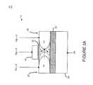
- FIGS. 2A and 2Bare exemplary cross-sectional illustrations of a memory cell using SOI and bulk semiconductor technologies, respectively, according to exemplary embodiments of the present inventions;
- FIGS. 3A and 3Bare exemplary cross-sectional illustrations of a memory cell according to the present inventions, in conjunction with exemplary control voltages applied to various regions or portions of the memory cell to program the memory cell to logic state “1” (i.e., generate or provide an excess of majority carrier in the electrically floating body of the memory cell of FIGS. 2A and 2B ); notably, majority carriers in these exemplary embodiments are generated or provided (or substantially generated or provided) via punch-through electron impact ionization;
- FIGS. 4A and 4Bare exemplary cross-sectional illustrations of a memory cell according to the present inventions, in conjunction with exemplary control voltages applied to various regions or portions of the memory cell to program the memory cell to logic state “0” (i.e., provide relatively fewer majority carrier by removing from the electrically floating body region of the transistor of the memory cell of FIGS.
- majority carriersmay be removed through the drain region/terminal and/or the source region/terminal, and/or through both drain and source regions/terminals and/or punch-through area via application of control signals applied to the various regions or portions of the memory cell, for example, via application of a gate voltage/bias (i.e., voltage applied to the gate), which is higher than the holding gate voltage/bias, and a drain voltage/bias, which is lower than the voltage applied to the drain when writing logic state “1” (i.e., the drain voltage/bias for logic state “1”);
- a gate voltage/biasi.e., voltage applied to the gate
- a drain voltage/biaswhich is lower than the voltage applied to the drain when writing logic state “1” (i.e., the drain voltage/bias for logic state “1”);
- FIGS. 5A and 5Bare exemplary cross-sectional illustrations of a memory cell according to the present inventions, in conjunction with exemplary control voltages applied to various regions or portions of the memory cell to read the stored data state (i.e., sense the data state stored in the memory cell—that is, the charge carrier concentration in the electrically floating body region of the transistor which is representative of a predetermined data state of the memory cell of FIGS. 2A and 2B ); notably, in an exemplary embodiment, the data state of the memory cell may be determined by sensing or sampling the amount of the punch-through current provided/generated (or substantially provided/generated) in response to the application of a predetermined voltages on the gate and drain of the transistor of the memory cell using, for example, a sense amplifier;
- FIG. 6Aillustrates exemplary timing relationships and control signal waveform of (i) selected write control signals for programming or writing a logic state “0” into one or more N-channel type memory cells, (ii) programming or writing logic state “1” into one or more N-channel type memory cells, and (iii) reading one or more N-channel type memory cells, according to an exemplary embodiment of the present inventions;
- FIG. 6Billustrates exemplary timing relationships and control signal waveform of (i) selected write control signals for programming or writing a logic state “0” into one or more N-channel type memory cells, (ii) programming or writing logic state “1” into one or more N-channel type memory cells, and (iii) reading one or more N-channel type memory cells, according to an exemplary embodiment of the present inventions;
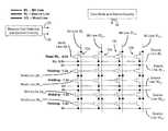
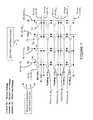
- FIGS. 7 and 8illustrate exemplary embodiments of a memory array having a plurality of memory cells and employing a separated source line configuration for each row of memory cells, in conjunction with exemplary programming techniques, including exemplary control signal voltage values ( FIG. 7 ) and exemplary reading techniques, including exemplary control signal voltage values ( FIG. 8 ), according to certain aspects of the present inventions;
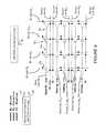
- FIGS. 9 and 10illustrate exemplary embodiments of a memory array having a plurality of memory cells and employing a common source line configuration for each row of memory cells in conjunction with exemplary programming techniques, including exemplary control signal voltage values ( FIG. 9 ), and exemplary reading techniques, including exemplary control signal voltage values ( FIG. 10 ), according to certain aspects of the present inventions;
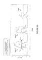
- FIG. 11illustrates non-disturbing reading of the proposed memory cell according to an exemplary embodiment of the present inventions.
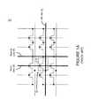
- FIGS. 12A-12Care schematic block diagram illustrations of exemplary integrated circuit devices in which the memory cell array (and certain peripheral circuitry) may be implemented, according to one or more aspects of the present inventions.
- the present inventionsare directed to techniques for reading, controlling and/or operating a semiconductor memory cell, array, and device having memory cells including at least one electrically floating body transistor in which electrical charge is stored in the body of the transistor.
- the present inventionsare also directed to semiconductor memory cell, array, architecture and device that include circuitry to implement such reading, controlling and/or operating techniques.
- the memory cell arraymay comprise a portion of an integrated circuit device, for example, a logic device (such as, a microcontroller or microprocessor) or a memory device (such as, a discrete memory device) having a plurality of memory cells.
- the inventive programming techniquesmay be implemented with or without employing a back gate or substrate terminals for SOI and bulk semiconductor technologies.
- the present inventionsin one aspect, describe a new memory cell and a combination of the programming/reading methods.
- the memory cellmay be implemented in a memory array which is disposed in/on a logic or discrete memory device.
- Such logic or discrete memory devicemay be smaller and consume less power in view of memory cells array implementing conventional architectures and techniques.
- the present inventionsmay be implemented on or in an SOI technology or a bulk semiconductor technology and may provide a memory cell comprising an electrically floating body transistor that is less sensitive to technology variations having improvement in retention characteristics relative to conventional architectures and techniques.
- the present inventionsemploy memory cell 12 including transistor 14 , having a body region, which is disposed on or in an SOI technology ( FIG. 2A ) or a bulk semiconductor technology ( FIG. 2B ).
- the transistor 14is configured, controlled and/or designed to operate in a punch-through mode.
- the junctions (or the depletion regions) between (i) source region 20 and body region 18 and (ii) drain region 22 and body region 18abut or overlap.
- the “punch-through” transistor 14is depicted as an N-channel type device. As such, majority carriers 34 are “holes”.
- the “punch-through” transistormay also be a P-channel type device. Under these circumstances, the majority carriers are electrons.
- the portion of the body region which is located immediately under gate 16 and/or gate oxide 32forms at least a portion (for example, a substantial portion) of the storage node of memory cell 12 .
- the portion of the body region which is located immediately under gate 16 and/or gate oxide 32is (sufficiently) electrically isolated from other portions of the body region of transistor 14 by the punch-through configuration.
- a portion of the chargemay be stored in the area close to the interface of insulation region 24 (for example, a buried silicon dioxide or other insulator).
- insulation region 24for example, a buried silicon dioxide or other insulator.
- the portion of the body region which is located immediately under gate 16 and/or gate oxide 32is (sufficiently) electrically isolated from other portions of the body region of transistor 14 as well as portions of the substrate which are beneath the source, drain and body regions.
- the punch-through transistormay be “optimized” and/or enhanced for the type of memory cell by adjusting the gate length, body doping and source/drain junctions.
- the generated majority carriersare, at least in part, stored in a portion of the body region that is located immediately under gate 16 and/or gate oxide 32 ( FIGS. 3A and 3B ).
- a portion of the chargemay be stored in the area close to the interface of insulation region 24 (for example, a buried silicon dioxide or other insulator) (see, FIG. 3A ).
- majority carriersare removed from the body region of transistor 14 .
- the majority carriersmay be removed, eliminated and/or ejected from the body region of transistor 14 through (i) source region 20 , (ii) drain region, or (iii) source region 20 and drain region 22 .
- the majority carriersmay be removed, eliminated and/or ejected from the body region via punch-through. (See, FIGS. 4A and 4B ).
- Such signalsinduce and/or cause a punch-through current.
- the amount of the punch-through currentis, at least in part, determined or defined by the amount of charge stored in transistor 14 .
- the data state of memory cell 12may be determined by sensing, sampling, reading and/or determining the punch-through current using data sense circuitry, for example, sense amplifier circuitry (such as a cross-coupled sense amplifier).
- control signals having a predetermined amplitudemay be selectively applied to a row of memory cells (for example, memory cells 12 a - d , which are coupled to word lines 28 i ) to write logic state “1” into selected memory cells 12 a and 12 d , and logic state “0” into selected memory cells 12 b and 12 c .
- a logic state “1”may be programmed or written in memory cells 12 a and 12 d by applying a voltage pulse of +2V to source region 20 of the transistors of memory cells 12 a and 12 d and a voltage pulse of +0.5V to gate 16 of the transistors of memory cells 12 a and 12 d .
- the source pulsemay be applied before the gate pulse, simultaneously thereto, or after the gate pulse is applied to gate 16 of the transistors of memory cells 12 a and 12 d .
- the source pulsebe applied to source region 20 of the transistors of memory cells 12 a and 12 d with a sufficient amplitude to maintain a sufficient punch-through current to program a logic state “1” into memory cells 12 a and 12 d . From a relative timing perspective, it is preferred that the source pulse extends beyond when the gate pulse reduces or ceases. (See, for example, FIGS. 6A and 6B ).
- control signals having predetermined amplitudesmay be applied to the transistors of memory cells 12 b and 12 c to write or program logic state “0” therein.
- the source pulsemay be applied to source region 20 of the transistors of memory cells 12 b and 12 c before the gate pulse is applied to gate 16 of the transistors of memory cells 12 b and 12 c , or simultaneously thereto, or after the gate pulse is applied to gate 16 of the transistors of memory cells 12 b and 12 c .
- a drain pulse(0.5V amplitude in this example) is applied to drain regions 22 of the transistors of memory cells 12 b and 12 d to prevent, prohibit, limit and/or retard a punch-through current from causing or generating a sufficient charge in the floating body region of memory cells 12 b and 12 c to program or write a logic state “1” into memory cells 12 b and 12 c .
- the drain pulsemay be characterized as a “blocking” pulse.
- the drain pulsebe applied to drain region 22 of the transistors of memory cells 12 b and 12 c for a temporal period that is applied before, during and after the source and gate pulses, for example, initiates, starts, ramps, declines and/or terminates), (See, for example, FIGS. 6A and 6B ).
- a holding conditionmay be applied or established to prevent, minimize and/or avoid disturbance of the data state of, or charge stored in the unselected memory cells.
- a voltagefor example, ⁇ 1.2V
- a voltagefor example, 0V
- the data state of the unselected memory cellsmay be unaffected (or substantially unaffected) by the programming of or writing to selected memory cells 12 a - 12 d.
- control signals having a predetermined amplitudemay be selectively applied to a row of memory cells (for example, memory cells 12 a - 12 d which are coupled to word lines 28 i ) to read the data state in each of the selected memory cells 12 a - 12 d .
- a voltage pulse of +0.5Vmay be applied to source region 20
- a voltage pulse of ⁇ 0.8Vmay be applied to gate 16 of the transistors of memory cells 12 a - 12 d .
- the source pulsemay be applied to source region 20 before application of the gate pulse to gate 16 , simultaneously thereto, or after the gate pulse is applied to gate 16 of the transistors of memory cells 12 a - 12 d . Further, the source pulse may cease or terminate before the gate pulse, simultaneously thereto (as illustrated in FIGS. 6A and 6B ), or after the gate pulse concludes or ceases.
- a holding conditionmay be applied or established to prevent, minimize and/or avoid disturbance of the data state in the unselected memory cells.
- a voltagefor example, ⁇ 1.2V
- a voltagefor example, 0V
- the state of the unselected memory cellsmay be unaffected (or substantially unaffected) during the reading of selected memory cells 12 a - 12 d.
- readingmay be performed many times in sequence without losing a detrimental amount of charge stored in the body region of the transistor.
- the memory cellmay undergo multiple read operations without the loss of an amount of charge that would result in destruction of the data state (i.e., the data state of the memory cell being undeterminable by sensing circuitry, for example, a sense amplifier).
- the illustrated/exemplary voltage levels to implement the write and read operationsare merely exemplary.
- the indicated voltage levelsmay be relative or absolute.
- the voltages indicatedmay be relative in that each voltage level, for example, may be increased or decreased by a given voltage amount (for example, each voltage may be increased or decreased by 0.25, 0.5, 1.0 and 2.0 volts) whether one or more of the voltages (for example, the source, drain or gate voltages) become or are positive and negative.
- the reading technique described hereinmay reduce the degradation of the charge in the electrically floating body which results from or is caused by charge-pumping (charge-pumping disturb).
- charge-pumping disturbcharge-pumping disturb
- the memory cellprovides a quasi non-disturbing reading.
- the read windowremains relatively stable for each successive read operation. (See, for example, FIG. 11 ).
- the memory cells of the memory array(s)may be comprised of N-channel, P-channel and/or both types of transistors. Further, circuitry that is peripheral to the memory array (for example, sense amplifiers or comparators, row and column address decoders, as well as line drivers (not illustrated herein)) may include P-channel and/or N-channel type transistors. Where P-channel type transistors are employed as memory cells 12 in the memory array(s), suitable write and read voltages (for example, negative voltages) are well known to those skilled in the art in light of this disclosure.
- a memory cell which is includes an electrically floating body transistor, which state is read/programmed using the techniques of the present inventionmay be employed in any array, architecture, layout, structure and/or configuration employing such memory cells.
- an electrically floating body transistor, which state is programmed and/or read using the techniques of the present inventionmay be implemented in the memory cell, architecture, layout, structure and/or configuration described and illustrated in the following non-provisional U.S. patent applications:
- the memory cells of the present inventionsmay be implemented in any memory array having, for example, a plurality of rows and columns (for example, in a matrix form).
- the present inventionsmay be implemented in any memory cell and/or memory cell array having an electrically floating body transistor.
- the present inventionsmay be employed in a memory array, having a plurality of memory cells each including an electrically floating body transistor wherein such memory cells are written, controlled, programmed and/or read according to any of the techniques described and/or illustrated herein.
- the data states of adjacent memory cells and/or memory cells that share a word linemay be individually and selectively programmed.
- memory cells having P-type or N-type transistorsmay be employed in any of the embodiments described and/or illustrated herein.
- all permutations and combinations of the memory cells with such embodiments and/or features thereof,are intended to come within the scope of the present inventions. For the sake of brevity, such permutations and combinations are not discussed in detail herein.
- the memory cellsinclude at least one electrically floating body transistor to store a charge in the electrically floating body region
- transistorsmay be symmetrical or non-symmetrical.
- the source and drain regionsare essentially interchangeable.
- the source or drain regions of transistorshave different electrical, physical, doping concentration and/or doping profile characteristics.
- the source or drain regions of a non-symmetrical deviceare typically not interchangeable.
- the drain region of the electrically floating N-channel type transistor of the memory cellis that region of the transistor that is connected to the bit line/sense amplifier.
- the inventions (and embodiments thereof) described and illustrated hereinare entirely applicable to N-channel and/or P-channel type transistors.
- the discussion described and illustratedonly source and drain implants, other implants may also be included.
- implants to modify the operation of memory cells 12which affect, for example, the power consumption of memory cells 12 as described and illustrated in (1) U.S. Pat. No. 6,969,662 (identified above), (2) U.S. Pat. No. 7,061,050 (identified above), and (3) Provisional Application Ser. No. 60/578,631, which was filed on Jun. 10, 2004 and entitled “Asymmetrical Electrically Floating Body Memory Device, and Method of Manufacturing Same”.
- the memory arraysmay be comprised of N-channel type transistors, P-channel type transistors and/or both types of transistors, as well as partially depleted and/or fully depleted type transistors.
- circuitry that is peripheral to the memory arraymay include fully depleted type transistors (whether P-channel and/or N-channel type).
- circuitrymay include partially depleted type transistors (whether P-channel and/or N-channel type).
- memory cell selection circuitrymay employ any circuitry and/or technique now known or later developed to select one or more memory cells for reading and/or programming. Indeed, all such techniques and circuitry therefor, whether now known or later developed, are intended to fall within the scope of the present inventions.
- data write and sense circuitrymay employ any circuitry whether now known or later developed.
- the data write and sense circuitrymay employ a sense amplifier to read the data stored in memory cells 12 .
- the sense amplifiermay sense the data state stored in memory cell 12 using voltage or current sensing techniques.
- a current sense amplifierfor example, Non-Provisional U.S. patent application Ser. No. 11/299,590 (U.S. Patent Application Publication US 2006/0126374), filed by Waller and Carman, on Dec. 12, 2005 and entitled “Sense Amplifier Circuitry and Architecture to Write Data into and/or Read Data from Memory Cells”
- the sense amplifiermay compare the memory cell current to a reference current, for example, the current of a reference cell.
- the data state of memory cell 12may be determined (for example, whether the memory cell 12 contained a logic high (relatively more majority carries 34 contained within body region 18 ) or logic low data state (relatively less majority carries 34 contained within body region 18 )).
- the reference current or voltagemay be substantially equal to one-half of the summation of the currents in a first reference cell, which has a logic low data state, and a second reference cell, which has a logic high data state. Other reference current or voltage levels are suitable.
- a reference generator circuitryis described in the context of generating, providing and/or supplying a reference current or voltage.
- the circuitry and techniques described and illustrated in U.S. patent application Ser. No. 10/840,902which was filed by Portmann et al. on May 7, 2004, and entitled “Reference Current Generator, and Method of Programming, Adjusting and/or Operating Same” (now U.S. Pat. No. 6,912,150), may be employed to generate an appropriate reference current for the data write and sense circuitry.
- the entire contents of U.S. patent application Ser. No. 10/840,902including, for example, the inventions, features, attributes, architectures, configurations, materials, techniques and advantages described and illustrated therein, are hereby incorporated by reference herein.
- present inventionshave been described in the exemplary embodiments as a single-bit memory cell, the present inventions may be implemented in memory cells that store more than one bit of data.
- present inventionsmay be implemented in conjunction with the inventions, embodiments, memory cells, memory cell arrays and architectures described and/or illustrated in U.S. Non-Provisional patent application Ser. No. 11/703,429, which was filed by Okhonin et al, on Feb. 7, 2007, and entitled “Multi-Bit Memory Cell Having Electrically Floating Body Transistor, and Method of Programming and Reading Same”.
- the multi-bit memory cell, and circuitry and techniques for reading, writing and/or operating a multi-bit memory cellmay be programmed using the techniques described and illustrated herein.
- the multi-bit memory cellstores more than one data bit (for example, two, three, four, five, six, etc.) and/or more than two data states (for example, three, four, five, six, etc. data or logic states).
- An analog-to-digital converter circuitry and/or one or more sense amplifiersmay be employed to read the multi-bit data stored in a memory cell (having an electrically floating body transistor).
- the sense amplifiermay sense the data state stored in the memory cell using voltage or current sensing techniques.
- the current sense amplifiermay compare the cell current to one or more reference currents, for example, the current of a reference cell (not illustrated). From that comparison, the data state of the memory cell may be determined (which is indicative of the number of majority carriers contained within electrically floating body region of the transistor).
- the present inventionsmay employ the circuitry and techniques for independently controlling certain parameters (for example, temporal or voltage), for a memory operation (for example, restore, write, refresh), to program or write a predetermined data state into a memory cell (for example, programming or writing data state “1” or “0” into a memory cell) as described and illustrated in U.S. patent application Ser. No. 11/590,147, which was filed by Popoff et al. on Oct. 31, 2006, and entitled “Method and Apparatus for Varying the Programming Duration and/or Voltage of an Electrically Floating Body Transistor, and Memory Cell Array Implementing Same”.
- certain parametersfor example, temporal or voltage
- a memory operationfor example, restore, write, refresh
- program or write a predetermined data state into a memory cellfor example, programming or writing data state “1” or “0” into a memory cell
- the duration of programming/writing/refreshing of a given memory state into a memory cell by data write and sense circuitrymay be controlled, adjusted, determined and/or predetermined according to or based on the given memory operation (for example, restore, write, refresh).
- the voltage conditions applied to the memory cell for programming/writing a given memory state into a memory cell by data write and sense circuitrymay be controlled and/or adjusted according to the memory operation (for example, restore, write, refresh).
- the transistors, memory cells and arraysmay be fabricated using well known techniques and/or materials. Indeed, any fabrication technique and/or material, whether now known or later developed, may be employed to fabricate the memory cells, transistors and/or memory array(s).
- the present inventionsmay employ silicon (whether bulk-type or SOI), germanium, silicon/germanium, gallium arsenide or any other semiconductor material in which transistors may be formed.
- the electrically floating body transistors, memory cells, and/or memory array(s)may employ the techniques described and illustrated in non-provisional patent application entitled “Integrated Circuit Device, and Method of Fabricating Same”, which was filed on Jul. 2, 2004, by Fazan, Ser. No. 10/884,481 (U.S.
- an integrated circuit deviceincludes memory section (having, for example, PD or FD SOI memory transistors) and logic section (having, for example, high performance transistors, such as FinFET, multiple gate transistors, and/or non-high performance transistors (for example, single gate transistors that do not possess the performance characteristics of high performance transistors—not illustrated)).
- memory sectionhaving, for example, PD or FD SOI memory transistors
- logic sectionhaving, for example, high performance transistors, such as FinFET, multiple gate transistors, and/or non-high performance transistors (for example, single gate transistors that do not possess the performance characteristics of high performance transistors—not illustrated)).
- the memory cell and/or memory cell array, as well as the circuitry of the present inventionsmay be implemented in an integrated circuit device having a memory portion and a logic portion (see, for example, FIGS. 12A and 12C ), or an integrated circuit device that is primarily a memory device (see, for example, FIG. 12B ).
- the memory arraymay include a plurality of memory cells arranged in a plurality of rows and columns wherein each memory cell includes a transistor (whether fabricated in a bulk-type material or SOI material), for example, an electrically floating body transistor.
- the memory arraysmay be comprised of N-channel, P-channel and/or both types of transistors.
- circuitry that is peripheral to the memory arraymay include P-channel and/or N-channel type transistors.
- circuitry that is peripheral to the memory arraymay be comprised of N-channel, P-channel and/or both types of transistors, as well as partially depleted and/or fully depleted type transistors.
- sense amplifiers or comparators, row and column address decoders, as well as line drivers (not illustrated herein)may include fully depleted type transistors (whether P-channel and/or N-channel type).
- circuitrymay include partially depleted type transistors (whether P-channel and/or N-channel type).
- There are many techniques to integrate both partially depleted and/or fully depleted type transistors on the same substratesee, for example, U.S. Non-Provisional patent application Ser. No. 10/487,157 (U.S. Patent Application Publication No. 2004/0238890), which was filed by Fazan et al. on Feb. 18, 2004 and entitled “Semiconductor Device”. All such techniques, whether now known or later developed, are intended to fall within the scope of the present inventions.
- transistors of the memory cellsmay be a symmetrical or non-symmetrical device. Where transistor is symmetrical, the source and drain regions are essentially interchangeable. However, where transistor is a non-symmetrical device, the source or drain regions of transistor have different electrical, physical, doping concentration and/or doping profile characteristics. As such, the source or drain regions of a non-symmetrical device are typically not interchangeable. This notwithstanding, the drain region of the electrically floating N-channel transistor of the memory cell (whether the source and drain regions are interchangeable or not) is that region of the transistor that is connected to the bit line/sense amplifier.
- each memory cell in the exemplary embodimentsincludes one transistor
- the memory cellmay include two transistors, as described and illustrated in application Ser. No. 10/829,877, which was filed by Ferrant et al. on Apr. 22, 2004 and entitled “Semiconductor Memory Cell, Array, Architecture and Device, and Method of Operating Same” (U.S. Patent Application Publication No. US 2005/0013163). For the sake of brevity, those discussions will not be repeated.
- the illustrated/exemplary voltage levels to implement the read and write operationsare merely exemplary.
- the indicated voltage levelsmay be relative or absolute.
- the voltages indicatedmay be relative in that each voltage level, for example, may be increased or decreased by a given voltage amount (for example, each voltage may be increased or decreased by 0.1, 0.15, 0.25, 0.5, 1, 2 (etc) volts) whether one or more of the voltages (for example, the source, drain or gate voltages) become or are positive and negative.
- circuitmeans, among other things, a single component or a multiplicity of components (whether in integrated circuit form or otherwise), which are active and/or passive, and which are coupled together to provide or perform a desired operation.
- circuitrymeans, among other things, a circuit (whether integrated or otherwise), or a group of circuits (whether integrated or otherwise).
- to sense a/the data state stored in memory cellmeans, among other things, to sample, to sense, to read and/or to determine a/the data state stored in memory cell; “sensing a/the data state stored in memory cell”, “sensed a/the data state stored in memory cell” or the like shall have the same meaning.
Landscapes
- Engineering & Computer Science (AREA)
- Microelectronics & Electronic Packaging (AREA)
- Computer Hardware Design (AREA)
- Semiconductor Memories (AREA)
Abstract
Description
Claims (20)
Priority Applications (1)
| Application Number | Priority Date | Filing Date | Title |
|---|---|---|---|
| US13/092,704US8295078B2 (en) | 2006-05-02 | 2011-04-22 | Semiconductor memory cell and array using punch-through to program and read same |
Applications Claiming Priority (3)
| Application Number | Priority Date | Filing Date | Title |
|---|---|---|---|
| US79667106P | 2006-05-02 | 2006-05-02 | |
| US11/796,935US7933142B2 (en) | 2006-05-02 | 2007-04-30 | Semiconductor memory cell and array using punch-through to program and read same |
| US13/092,704US8295078B2 (en) | 2006-05-02 | 2011-04-22 | Semiconductor memory cell and array using punch-through to program and read same |
Related Parent Applications (1)
| Application Number | Title | Priority Date | Filing Date |
|---|---|---|---|
| US11/796,935ContinuationUS7933142B2 (en) | 2006-05-02 | 2007-04-30 | Semiconductor memory cell and array using punch-through to program and read same |
Publications (2)
| Publication Number | Publication Date |
|---|---|
| US20110194363A1 US20110194363A1 (en) | 2011-08-11 |
| US8295078B2true US8295078B2 (en) | 2012-10-23 |
Family
ID=38445608
Family Applications (2)
| Application Number | Title | Priority Date | Filing Date |
|---|---|---|---|
| US11/796,935Active2029-07-04US7933142B2 (en) | 2006-05-02 | 2007-04-30 | Semiconductor memory cell and array using punch-through to program and read same |
| US13/092,704ActiveUS8295078B2 (en) | 2006-05-02 | 2011-04-22 | Semiconductor memory cell and array using punch-through to program and read same |
Family Applications Before (1)
| Application Number | Title | Priority Date | Filing Date |
|---|---|---|---|
| US11/796,935Active2029-07-04US7933142B2 (en) | 2006-05-02 | 2007-04-30 | Semiconductor memory cell and array using punch-through to program and read same |
Country Status (2)
| Country | Link |
|---|---|
| US (2) | US7933142B2 (en) |
| WO (1) | WO2007128738A1 (en) |
Cited By (1)
| Publication number | Priority date | Publication date | Assignee | Title |
|---|---|---|---|---|
| WO2016029189A1 (en)* | 2014-08-22 | 2016-02-25 | Alacrity Semiconductors, Inc. | Methods and apparatus for memory programming |
Families Citing this family (10)
| Publication number | Priority date | Publication date | Assignee | Title |
|---|---|---|---|---|
| US9030867B2 (en) | 2008-10-20 | 2015-05-12 | Seagate Technology Llc | Bipolar CMOS select device for resistive sense memory |
| US7825478B2 (en) | 2008-11-07 | 2010-11-02 | Seagate Technology Llc | Polarity dependent switch for resistive sense memory |
| US8159856B2 (en) | 2009-07-07 | 2012-04-17 | Seagate Technology Llc | Bipolar select device for resistive sense memory |
| US8208285B2 (en)* | 2009-07-13 | 2012-06-26 | Seagate Technology Llc | Vertical non-volatile switch with punchthrough access and method of fabrication therefor |
| TWI451570B (en)* | 2011-11-15 | 2014-09-01 | Univ Nat Chiao Tung | Multi-bit resistance switching memory components and arrays |
| US9059292B2 (en) | 2012-08-02 | 2015-06-16 | International Business Machines Corporation | Source and drain doping profile control employing carbon-doped semiconductor material |
| US8841188B2 (en) | 2012-09-06 | 2014-09-23 | International Business Machines Corporation | Bulk finFET with controlled fin height and high-K liner |
| TWI485706B (en)* | 2013-02-07 | 2015-05-21 | Winbond Electronics Corp | Resistive memory and memory cell thereof |
| JP5754478B2 (en)* | 2013-07-24 | 2015-07-29 | ミツミ電機株式会社 | Power generation device, power generation device set and power generation system |
| CN116206643B (en)* | 2022-07-25 | 2024-03-15 | 北京超弦存储器研究院 | Dynamic random access memory unit, memory device and reading method |
Citations (298)
| Publication number | Priority date | Publication date | Assignee | Title |
|---|---|---|---|---|
| CA272437A (en) | 1925-10-22 | 1927-07-19 | Edgar Lilienfeld Julius | Electric current control mechanism |
| US3439214A (en) | 1968-03-04 | 1969-04-15 | Fairchild Camera Instr Co | Beam-junction scan converter |
| GB1414228A (en) | 1972-04-25 | 1975-11-19 | Ibm | Semiconductor storage devices |
| US3997799A (en) | 1975-09-15 | 1976-12-14 | Baker Roger T | Semiconductor-device for the storage of binary data |
| US4032947A (en) | 1971-10-20 | 1977-06-28 | Siemens Aktiengesellschaft | Controllable charge-coupled semiconductor device |
| US4250569A (en) | 1978-11-15 | 1981-02-10 | Fujitsu Limited | Semiconductor memory device |
| US4262340A (en) | 1978-11-14 | 1981-04-14 | Fujitsu Limited | Semiconductor memory device |
| US4298962A (en) | 1979-01-25 | 1981-11-03 | Nippon Electric Co., Ltd. | Memory |
| US4371955A (en) | 1979-02-22 | 1983-02-01 | Fujitsu Limited | Charge-pumping MOS FET memory device |
| EP0030856B1 (en) | 1979-12-13 | 1984-03-21 | Fujitsu Limited | Charge-pumping semiconductor memory cell comprising a charge-storage region and memory device using such a cell |
| US4527181A (en) | 1980-08-28 | 1985-07-02 | Fujitsu Limited | High density semiconductor memory array and method of making same |
| US4630089A (en) | 1983-09-27 | 1986-12-16 | Fujitsu Limited | Semiconductor memory device |
| US4658377A (en) | 1984-07-26 | 1987-04-14 | Texas Instruments Incorporated | Dynamic memory array with segmented bit lines |
| JPS62272561A (en) | 1986-05-20 | 1987-11-26 | Seiko Epson Corp | 1 transistor memory cell |
| US4791610A (en) | 1985-05-24 | 1988-12-13 | Fujitsu Limited | Semiconductor memory device formed of a SOI-type transistor and a capacitor |
| US4807195A (en) | 1987-05-18 | 1989-02-21 | International Business Machines Corporation | Apparatus and method for providing a dual sense amplifier with divided bit line isolation |
| EP0354348A2 (en) | 1988-08-10 | 1990-02-14 | International Business Machines Corporation | CMOS-transistor and one-capacitor dram cell and fabrication process therefor |
| US4954989A (en) | 1988-04-12 | 1990-09-04 | Commissariat A L'energie Atomique | MIS type static memory cell and memory and storage process |
| US4979014A (en) | 1987-08-10 | 1990-12-18 | Kabushiki Kaisha Toshiba | MOS transistor |
| EP0202515B1 (en) | 1982-11-04 | 1991-03-13 | Hitachi, Ltd. | Semiconductor memory |
| US5010524A (en) | 1989-04-20 | 1991-04-23 | International Business Machines Corporation | Crosstalk-shielded-bit-line dram |
| EP0175378B1 (en) | 1984-09-21 | 1991-11-21 | Fujitsu Limited | Dynamic random access memory (dram) |
| EP0253631B1 (en) | 1986-07-14 | 1992-04-22 | Oki Electric Industry Company, Limited | Semiconductor memory device |
| JPH04176163A (en) | 1990-11-08 | 1992-06-23 | Fujitsu Ltd | Semiconductor device and manufacture thereof |
| US5144390A (en) | 1988-09-02 | 1992-09-01 | Texas Instruments Incorporated | Silicon-on insulator transistor with internal body node to source node connection |
| US5164805A (en) | 1988-08-22 | 1992-11-17 | Massachusetts Institute Of Technology | Near-intrinsic thin-film SOI FETS |
| EP0300157B1 (en) | 1987-07-20 | 1993-05-05 | International Business Machines Corporation | Vertical transistor capacitor memory cell structure and fabrication method therefor |
| US5258635A (en) | 1988-09-06 | 1993-11-02 | Kabushiki Kaisha Toshiba | MOS-type semiconductor integrated circuit device |
| EP0350057B1 (en) | 1988-07-07 | 1993-12-01 | Kabushiki Kaisha Toshiba | Semiconductor memory |
| EP0362961B1 (en) | 1988-10-03 | 1994-02-16 | Interuniversitair Microelektronica Centrum Vzw | A method of operating a MOS-structure and MOS-structure therefor |
| US5313432A (en) | 1990-05-23 | 1994-05-17 | Texas Instruments Incorporated | Segmented, multiple-decoder memory array and method for programming a memory array |
| US5315541A (en) | 1992-07-24 | 1994-05-24 | Sundisk Corporation | Segmented column memory array |
| EP0599506A1 (en) | 1992-11-27 | 1994-06-01 | International Business Machines Corporation | Semiconductor memory cell with SOI MOSFET |
| US5350938A (en) | 1990-06-27 | 1994-09-27 | Kabushiki Kaisha Toshiba | Nonvolatile semiconductor memory circuit with high speed read-out |
| EP0564204A3 (en) | 1992-03-30 | 1994-09-28 | Mitsubishi Electric Corp | Semiconductor device |
| US5355330A (en) | 1991-08-29 | 1994-10-11 | Hitachi, Ltd. | Capacitive memory having a PN junction writing and tunneling through an insulator of a charge holding electrode |
| EP0359551B1 (en) | 1988-09-14 | 1994-12-28 | Kawasaki Steel Corporation | Semicoductor memory circuit |
| US5388068A (en) | 1990-05-02 | 1995-02-07 | Microelectronics & Computer Technology Corp. | Superconductor-semiconductor hybrid memory circuits with superconducting three-terminal switching devices |
| US5397726A (en) | 1992-02-04 | 1995-03-14 | National Semiconductor Corporation | Segment-erasable flash EPROM |
| EP0366882B1 (en) | 1988-10-31 | 1995-05-24 | International Business Machines Corporation | An ultra dense DRAM cell array and its method of fabrication |
| US5432730A (en) | 1993-12-20 | 1995-07-11 | Waferscale Integration, Inc. | Electrically programmable read only memory array |
| EP0465961B1 (en) | 1990-07-09 | 1995-08-09 | Sony Corporation | Semiconductor device on a dielectric isolated substrate |
| EP0579566A3 (en) | 1992-06-17 | 1995-08-09 | Ibm | High-density dram structure on SOI. |
| US5446299A (en) | 1994-04-29 | 1995-08-29 | International Business Machines Corporation | Semiconductor random access memory cell on silicon-on-insulator with dual control gates |
| US5448513A (en) | 1993-12-02 | 1995-09-05 | Regents Of The University Of California | Capacitorless DRAM device on silicon-on-insulator substrate |
| EP0513923B1 (en) | 1991-05-15 | 1995-09-27 | Koninklijke Philips Electronics N.V. | Protected programmable transistor with reduced parasitic capacitances and method of fabrication |
| US5489792A (en) | 1994-04-07 | 1996-02-06 | Regents Of The University Of California | Silicon-on-insulator transistors having improved current characteristics and reduced electrostatic discharge susceptibility |
| US5506436A (en) | 1992-12-10 | 1996-04-09 | Sony Corporation | Semiconductor memory cell |
| US5515383A (en) | 1991-05-28 | 1996-05-07 | The Boeing Company | Built-in self-test system and method for self test of an integrated circuit |
| US5526307A (en) | 1992-01-22 | 1996-06-11 | Macronix International Co., Ltd. | Flash EPROM integrated circuit architecture |
| EP0333426B1 (en) | 1988-03-15 | 1996-07-10 | Kabushiki Kaisha Toshiba | Dynamic RAM |
| JPH08213624A (en) | 1995-02-08 | 1996-08-20 | Fujitsu Ltd | Semiconductor memory device and operating method thereof |
| US5568356A (en) | 1995-04-18 | 1996-10-22 | Hughes Aircraft Company | Stacked module assembly including electrically interconnected switching module and plural electronic modules |
| EP0694977A3 (en) | 1994-07-14 | 1996-11-06 | Nec Corp | SOI-type semiconductor device with suppression of extension of the depletion region |
| JPH08316337A (en) | 1995-05-12 | 1996-11-29 | Nec Corp | Semiconductor memory device |
| US5583808A (en) | 1994-09-16 | 1996-12-10 | National Semiconductor Corporation | EPROM array segmented for high performance and method for controlling same |
| US5593912A (en) | 1994-10-06 | 1997-01-14 | International Business Machines Corporation | SOI trench DRAM cell for 256 MB DRAM and beyond |
| US5606188A (en) | 1995-04-26 | 1997-02-25 | International Business Machines Corporation | Fabrication process and structure for a contacted-body silicon-on-insulator dynamic random access memory |
| US5608250A (en) | 1993-11-29 | 1997-03-04 | Sgs-Thomson Microelectronics S.A. | Volatile memory cell with interface charge traps |
| EP0245515B1 (en) | 1985-11-20 | 1997-04-16 | Hitachi, Ltd. | Semiconductor device |
| US5627092A (en) | 1994-09-26 | 1997-05-06 | Siemens Aktiengesellschaft | Deep trench dram process on SOI for low leakage DRAM cell |
| US5631186A (en) | 1992-12-30 | 1997-05-20 | Samsung Electronics Co., Ltd. | Method for making a dynamic random access memory using silicon-on-insulator techniques |
| US5677867A (en) | 1991-06-12 | 1997-10-14 | Hazani; Emanuel | Memory with isolatable expandable bit lines |
| US5696718A (en) | 1994-11-10 | 1997-12-09 | Commissariat A L'energie Atomique | Device having an electrically erasable non-volatile memory and process for producing such a device |
| EP0510607B1 (en) | 1991-04-23 | 1998-02-04 | Canon Kabushiki Kaisha | Semiconductor memory device |
| US5740099A (en) | 1995-02-07 | 1998-04-14 | Nec Corporation | Semiconductor memory device having peripheral circuit and interface circuit fabricated on bulk region out of silicon-on-insulator region for memory cells |
| US5754469A (en) | 1996-06-14 | 1998-05-19 | Macronix International Co., Ltd. | Page mode floating gate memory device storing multiple bits per cell |
| US5774411A (en) | 1996-09-12 | 1998-06-30 | International Business Machines Corporation | Methods to enhance SOI SRAM cell stability |
| US5778243A (en) | 1996-07-03 | 1998-07-07 | International Business Machines Corporation | Multi-threaded cell for a memory |
| US5780906A (en) | 1995-06-21 | 1998-07-14 | Micron Technology, Inc. | Static memory cell and method of manufacturing a static memory cell |
| US5784311A (en) | 1997-06-13 | 1998-07-21 | International Business Machines Corporation | Two-device memory cell on SOI for merged logic and memory applications |
| EP0537677B1 (en) | 1991-10-16 | 1998-08-19 | Sony Corporation | Method of forming an SOI structure with a DRAM |
| US5798968A (en) | 1996-09-24 | 1998-08-25 | Sandisk Corporation | Plane decode/virtual sector architecture |
| EP0860878A2 (en) | 1997-02-20 | 1998-08-26 | Texas Instruments Incorporated | An integrated circuit with programmable elements |
| US5811283A (en) | 1996-08-13 | 1998-09-22 | United Microelectronics Corporation | Silicon on insulator (SOI) dram cell structure and process |
| US5847411A (en) | 1996-04-11 | 1998-12-08 | Matsushita Electric Industrial Co., Ltd. | Semiconductor device having a channel region including a vacancy-introduced polysilicon layer |
| US5877978A (en) | 1996-03-04 | 1999-03-02 | Mitsubishi Denki Kabushiki Kaisha | Semiconductor memory device |
| US5886385A (en) | 1996-08-22 | 1999-03-23 | Kabushiki Kaisha Toshiba | Semiconductor device and manufacturing method thereof |
| US5886376A (en) | 1996-07-01 | 1999-03-23 | International Business Machines Corporation | EEPROM having coplanar on-insulator FET and control gate |
| US5897351A (en) | 1997-02-20 | 1999-04-27 | Micron Technology, Inc. | Method for forming merged transistor structure for gain memory cell |
| EP0878804A3 (en) | 1997-05-15 | 1999-07-14 | STMicroelectronics, Inc. | Multiple transistor dynamic random access memory array architecture with simultaneous refresh of multiple memory cells during a read operation |
| EP0642173B1 (en) | 1993-08-19 | 1999-07-14 | Hitachi, Ltd. | Semiconductor element and semiconductor memory device using the same |
| US5930648A (en) | 1996-12-30 | 1999-07-27 | Hyundai Electronics Industries Co., Ltd. | Semiconductor memory device having different substrate thickness between memory cell area and peripheral area and manufacturing method thereof |
| US5929479A (en) | 1996-10-21 | 1999-07-27 | Nec Corporation | Floating gate type non-volatile semiconductor memory for storing multi-value information |
| US5936265A (en) | 1996-03-25 | 1999-08-10 | Kabushiki Kaisha Toshiba | Semiconductor device including a tunnel effect element |
| EP0727822B1 (en) | 1995-02-14 | 1999-08-11 | Canon Kabushiki Kaisha | Semiconductor memory device |
| US5943258A (en) | 1997-12-24 | 1999-08-24 | Texas Instruments Incorporated | Memory with storage cells having SOI drive and access transistors with tied floating body connections |
| US5943581A (en) | 1997-11-05 | 1999-08-24 | Vanguard International Semiconductor Corporation | Method of fabricating a buried reservoir capacitor structure for high-density dynamic random access memory (DRAM) circuits |
| US5977578A (en) | 1995-12-06 | 1999-11-02 | Micron Technology, Inc. | Method of forming dynamic random access memory circuitry and dynamic random access memory |
| US5986914A (en) | 1993-03-31 | 1999-11-16 | Stmicroelectronics, Inc. | Active hierarchical bitline memory architecture |
| US6018172A (en) | 1994-09-26 | 2000-01-25 | Mitsubishi Denki Kabushiki Kaisha | Semiconductor memory device including memory cell transistors formed on SOI substrate and having fixed body regions |
| US6048756A (en) | 1997-07-31 | 2000-04-11 | Electronics And Telecommunications Research Institute | Method for making a silicon-on-insulator MOS transistor using a selective SiGe epitaxy |
| US6097624A (en) | 1997-09-17 | 2000-08-01 | Samsung Electronics Co., Ltd. | Methods of operating ferroelectric memory devices having reconfigurable bit lines |
| US6097056A (en) | 1998-04-28 | 2000-08-01 | International Business Machines Corporation | Field effect transistor having a floating gate |
| US6096598A (en) | 1998-10-29 | 2000-08-01 | International Business Machines Corporation | Method for forming pillar memory cells and device formed thereby |
| EP0599388B1 (en) | 1992-11-20 | 2000-08-02 | Koninklijke Philips Electronics N.V. | Semiconductor device provided with a programmable element |
| EP0689252B1 (en) | 1990-03-20 | 2000-08-02 | Nec Corporation | Semiconductor device |
| US6111778A (en) | 1999-05-10 | 2000-08-29 | International Business Machines Corporation | Body contacted dynamic memory |
| EP0682370B1 (en) | 1994-05-13 | 2000-09-06 | Canon Kabushiki Kaisha | Storage device |
| JP2000247735A (en) | 1999-03-01 | 2000-09-12 | Murata Mfg Co Ltd | Production of low-temperature sintered ceramic composition |
| US6133597A (en) | 1997-07-25 | 2000-10-17 | Mosel Vitelic Corporation | Biasing an integrated circuit well with a transistor electrode |
| US6157216A (en) | 1999-04-22 | 2000-12-05 | International Business Machines Corporation | Circuit driver on SOI for merged logic and memory circuits |
| US6171923B1 (en) | 1997-11-20 | 2001-01-09 | Vanguard International Semiconductor Corporation | Method for fabricating a DRAM cell structure on an SOI wafer incorporating a two dimensional trench capacitor |
| US6177708B1 (en) | 1998-08-07 | 2001-01-23 | International Business Machines Corporation | SOI FET body contact structure |
| US6177698B1 (en) | 1999-02-01 | 2001-01-23 | Infineon Technologies North America Corp. | Formation of controlled trench top isolation layers for vertical transistors |
| US6214694B1 (en) | 1998-11-17 | 2001-04-10 | International Business Machines Corporation | Process of making densely patterned silicon-on-insulator (SOI) region on a wafer |
| US6222217B1 (en) | 1997-11-27 | 2001-04-24 | Mitsubishi Denki Kabushiki Kaisha | Semiconductor device and manufacturing method thereof |
| US6225158B1 (en) | 1998-05-28 | 2001-05-01 | International Business Machines Corporation | Trench storage dynamic random access memory cell with vertical transfer device |
| US6252281B1 (en) | 1995-03-27 | 2001-06-26 | Kabushiki Kaisha Toshiba | Semiconductor device having an SOI substrate |
| US6262935B1 (en) | 2000-06-17 | 2001-07-17 | United Memories, Inc. | Shift redundancy scheme for wordlines in memory circuits |
| US6292424B1 (en) | 1995-01-20 | 2001-09-18 | Kabushiki Kaisha Toshiba | DRAM having a power supply voltage lowering circuit |
| EP0920059A3 (en) | 1997-11-28 | 2001-09-26 | Infineon Technologies AG | Memory cell array and method of producing the same |
| US6297090B1 (en) | 1998-08-14 | 2001-10-02 | Samsung Electronics Co., Ltd. | Method for fabricating a high-density semiconductor memory device |
| US6320227B1 (en) | 1998-12-26 | 2001-11-20 | Hyundai Electronics Industries Co., Ltd. | Semiconductor memory device and method for fabricating the same |
| US6333866B1 (en) | 1998-09-28 | 2001-12-25 | Texas Instruments Incorporated | Semiconductor device array having dense memory cell array and heirarchical bit line scheme |
| US6333532B1 (en) | 1999-07-16 | 2001-12-25 | International Business Machines Corporation | Patterned SOI regions in semiconductor chips |
| US20010055859A1 (en) | 2000-06-26 | 2001-12-27 | Kabushiki Kaisha Toshiba | Semiconductor device and method of fabricating the same |
| US6351426B1 (en) | 1995-01-20 | 2002-02-26 | Kabushiki Kaisha Toshiba | DRAM having a power supply voltage lowering circuit |
| US6350653B1 (en) | 2000-10-12 | 2002-02-26 | International Business Machines Corporation | Embedded DRAM on silicon-on-insulator substrate |
| US20020030214A1 (en) | 2000-09-11 | 2002-03-14 | Fumio Horiguchi | Semiconductor device and method for manufacturing the same |
| US6359802B1 (en) | 2000-03-28 | 2002-03-19 | Intel Corporation | One-transistor and one-capacitor DRAM cell for logic process technology |
| US20020034855A1 (en) | 2000-09-08 | 2002-03-21 | Fumio Horiguchi | Semiconductor memory device and its manufacturing method |
| US20020036322A1 (en) | 2000-03-17 | 2002-03-28 | Ramachandra Divakauni | SOI stacked dram logic |
| US20020051378A1 (en) | 2000-08-17 | 2002-05-02 | Takashi Ohsawa | Semiconductor memory device and method of manufacturing the same |
| US6391658B1 (en) | 1999-10-26 | 2002-05-21 | International Business Machines Corporation | Formation of arrays of microelectronic elements |
| US6403435B1 (en) | 2000-07-21 | 2002-06-11 | Hyundai Electronics Industries Co., Ltd. | Method for fabricating a semiconductor device having recessed SOI structure |
| EP1162663A8 (en) | 2000-06-06 | 2002-06-12 | Infineon Technologies AG | DRAM memory cell for DRAM memory device and method of making the same |
| US20020072155A1 (en) | 2000-12-08 | 2002-06-13 | Chih-Cheng Liu | Method of fabricating a DRAM unit |
| US20020070411A1 (en) | 2000-09-08 | 2002-06-13 | Alcatel | Method of processing a high voltage p++/n-well junction and a device manufactured by the method |
| US20020076880A1 (en) | 2000-06-12 | 2002-06-20 | Takashi Yamada | Semiconductor device and method of fabricating the same |
| US20020086463A1 (en) | 2000-12-30 | 2002-07-04 | Houston Theodore W. | Means for forming SOI |
| US20020089038A1 (en) | 2000-10-20 | 2002-07-11 | International Business Machines Corporation | Fully-depleted-collector silicon-on-insulator (SOI) bipolar transistor useful alone or in SOI BiCMOS |
| US6421269B1 (en) | 2000-10-17 | 2002-07-16 | Intel Corporation | Low-leakage MOS planar capacitors for use within DRAM storage cells |
| US6424011B1 (en) | 1997-04-14 | 2002-07-23 | International Business Machines Corporation | Mixed memory integration with NVRAM, dram and sram cell structures on same substrate |
| US6424016B1 (en) | 1996-05-24 | 2002-07-23 | Texas Instruments Incorporated | SOI DRAM having P-doped polysilicon gate for a memory pass transistor |
| EP1209747A3 (en) | 1995-02-17 | 2002-07-24 | Hitachi, Ltd. | Semiconductor memory element |
| US20020098643A1 (en) | 1997-02-28 | 2002-07-25 | Kabushiki Kaisha Toshiba | Method of manufacturing SOI element having body contact |
| US6429477B1 (en) | 2000-10-31 | 2002-08-06 | International Business Machines Corporation | Shared body and diffusion contact structure and method for fabricating same |
| US6432769B1 (en) | 1995-10-27 | 2002-08-13 | Hitachi, Ltd. | Semiconductor integrated circuit device and process for manufacture the same |
| EP0744772B1 (en) | 1995-05-24 | 2002-08-14 | Infineon Technologies AG | DRAM storage cell with vertical transistor and method for production thereof |
| US20020110018A1 (en) | 2001-02-15 | 2002-08-15 | Takashi Ohsawa | Semiconductor memory device |
| EP1233454A2 (en) | 2001-02-19 | 2002-08-21 | Kabushiki Kaisha Toshiba | Semiconductor memory device and method of manufacturing the same |
| US6441435B1 (en) | 2001-01-31 | 2002-08-27 | Advanced Micro Devices, Inc. | SOI device with wrap-around contact to underside of body, and method of making |
| US6441436B1 (en) | 2000-11-29 | 2002-08-27 | United Microelectronics Corp. | SOI device and method of fabrication |
| US6440872B1 (en) | 2000-11-03 | 2002-08-27 | International Business Machines Corporation | Method for hybrid DRAM cell utilizing confined strap isolation |
| EP1241708A2 (en) | 2001-03-15 | 2002-09-18 | Kabushiki Kaisha Toshiba | Semiconductor memory device with floating body |
| EP0725402B1 (en) | 1995-01-05 | 2002-09-25 | Kabushiki Kaisha Toshiba | Semiconductor memory device |
| US6466511B2 (en) | 2000-06-30 | 2002-10-15 | Kabushiki Kaisha Toshiba | Semiconductor memory having double data rate transfer technique |
| US20020160581A1 (en) | 2001-04-26 | 2002-10-31 | Shinichi Watanabe | Semiconductor device |
| US6480407B1 (en) | 1995-08-25 | 2002-11-12 | Micron Technology, Inc. | Reduced area sense amplifier isolation layout in a dynamic RAM architecture |
| US6479862B1 (en) | 2000-06-22 | 2002-11-12 | Progressant Technologies, Inc. | Charge trapping device and method for implementing a transistor having a negative differential resistance mode |
| JP2002329795A (en) | 2001-04-26 | 2002-11-15 | Toshiba Corp | Semiconductor memory device and method of manufacturing the same |
| JP2002343886A (en) | 2001-03-15 | 2002-11-29 | Toshiba Corp | Semiconductor memory device |
| JP2002353080A (en) | 2001-03-21 | 2002-12-06 | Toshiba Corp | Semiconductor wafer, semiconductor device manufacturing apparatus, semiconductor device manufacturing method, and semiconductor wafer manufacturing method |
| US6492211B1 (en) | 2000-09-07 | 2002-12-10 | International Business Machines Corporation | Method for novel SOI DRAM BICMOS NPN |
| US20030015757A1 (en) | 2001-07-19 | 2003-01-23 | Takashi Ohsawa | Semiconductor memory device |
| US6518105B1 (en) | 2001-12-10 | 2003-02-11 | Taiwan Semiconductor Manufacturing Company | High performance PD SOI tunneling-biased MOSFET |
| US20030035324A1 (en) | 2001-08-17 | 2003-02-20 | Kabushiki Kaisha Toshiba | Semiconductor memory device |
| US20030042516A1 (en) | 2001-08-30 | 2003-03-06 | Micron Technology, Inc. | Technique to control tunneling currents in dram capacitors, cells, and devices |
| US6531754B1 (en) | 2001-12-28 | 2003-03-11 | Kabushiki Kaisha Toshiba | Manufacturing method of partial SOI wafer, semiconductor device using the partial SOI wafer and manufacturing method thereof |
| US20030047784A1 (en) | 1999-07-23 | 2003-03-13 | Mitsubishi Denki Kabushiki Kaisha | Semiconductor device |
| US6537871B2 (en) | 1997-10-06 | 2003-03-25 | Micron Technology, Inc. | Circuit and method for an open bit line memory cell with a vertical transistor and trench plate trench capacitor |
| US20030057490A1 (en) | 2001-09-26 | 2003-03-27 | Kabushiki Kaisha Toshiba | Semiconductor device substrate and method of manufacturing semiconductor device substrate |
| US20030057487A1 (en) | 2001-09-27 | 2003-03-27 | Kabushiki Kaisha Toshiba | Semiconductor chip having multiple functional blocks integrated in a single chip and method for fabricating the same |
| US6549450B1 (en) | 2000-11-08 | 2003-04-15 | Ibm Corporation | Method and system for improving the performance on SOI memory arrays in an SRAM architecture system |
| US6552398B2 (en) | 2001-01-16 | 2003-04-22 | Ibm Corporation | T-Ram array having a planar cell structure and method for fabricating the same |
| US6552932B1 (en) | 2001-09-21 | 2003-04-22 | Sandisk Corporation | Segmented metal bitlines |
| US6556477B2 (en) | 2001-05-21 | 2003-04-29 | Ibm Corporation | Integrated chip having SRAM, DRAM and flash memory and method for fabricating the same |
| US6560142B1 (en) | 2002-03-22 | 2003-05-06 | Yoshiyuki Ando | Capacitorless DRAM gain cell |
| JP2003132682A (en) | 2001-08-17 | 2003-05-09 | Toshiba Corp | Semiconductor memory device |
| US6563733B2 (en) | 2001-05-24 | 2003-05-13 | Winbond Electronics Corporation | Memory array architectures based on a triple-polysilicon source-side injection non-volatile memory cell |
| US6566177B1 (en) | 1999-10-25 | 2003-05-20 | International Business Machines Corporation | Silicon-on-insulator vertical array device trench capacitor DRAM |
| US6573566B2 (en) | 2001-07-09 | 2003-06-03 | United Microelectronics Corp. | Low-voltage-triggered SOI-SCR device and associated ESD protection circuit |
| US6574135B1 (en) | 2002-04-19 | 2003-06-03 | Texas Instruments Incorporated | Shared sense amplifier for ferro-electric memory cell |
| US20030102497A1 (en) | 2001-12-04 | 2003-06-05 | International Business Machines Corporation | Multiple-plane finFET CMOS |
| US20030123279A1 (en) | 2002-01-03 | 2003-07-03 | International Business Machines Corporation | Silicon-on-insulator SRAM cells with increased stability and yield |
| US20030146474A1 (en) | 2002-02-05 | 2003-08-07 | Industrial Technology Research Institute | SCR devices in silicon-on-insulator CMOS process for on-chip ESD protection |
| US20030151112A1 (en) | 2002-02-13 | 2003-08-14 | Takashi Yamada | Semiconductor device having one of patterned SOI and SON structure |
| EP1162744B1 (en) | 2000-06-05 | 2003-09-10 | Mitsubishi Denki Kabushiki Kaisha | Semiconductor integrated circuit device operating with low power consumption |
| EP1073121A3 (en) | 1999-07-29 | 2003-10-29 | Fujitsu Limited | Semiconductor memory device and method for manufacturing the same |
| US6650565B1 (en) | 2002-09-11 | 2003-11-18 | Kabushiki Kaisha Toshiba | Semiconductor memory device |
| US6653175B1 (en) | 2001-03-22 | 2003-11-25 | T-Ram, Inc. | Stability in thyristor-based memory device |
| US20030231521A1 (en) | 2002-06-18 | 2003-12-18 | Kabushiki Kaisha Toshiba | Semiconductor memory device and semiconductor device |
| US6686624B2 (en) | 2002-03-11 | 2004-02-03 | Monolithic System Technology, Inc. | Vertical one-transistor floating-body DRAM cell in bulk CMOS process with electrically isolated charge storage region |
| EP0788165B1 (en) | 1996-02-02 | 2004-02-04 | Infineon Technologies AG | Storage cell arrangement and method for making the same |
| US20040021137A1 (en) | 2001-06-18 | 2004-02-05 | Pierre Fazan | Semiconductor device |
| US20040021179A1 (en) | 2002-08-05 | 2004-02-05 | Byeong-Chan Lee | Metal oxide semiconductor transistors having a drain punch through blocking region and methods for fabricating metal oxide semiconductor transistors having a drain punch through blocking region |
| US20040029335A1 (en) | 2001-02-27 | 2004-02-12 | Aplus Flash Technology, Inc. | Novel set of three level concurrent word line bias conditions for a NOR type flash memory array |
| US6707118B2 (en) | 2000-03-31 | 2004-03-16 | Intel Corporation | Semiconductor-on-insulator resistor-capacitor circuit |
| US6714436B1 (en) | 2003-03-20 | 2004-03-30 | Motorola, Inc. | Write operation for capacitorless RAM |
| EP0739097B1 (en) | 1995-04-21 | 2004-04-07 | Nippon Telegraph And Telephone Corporation | MOSFET circuit and CMOS logic circuit using the same |
| US6721222B2 (en) | 2000-10-17 | 2004-04-13 | Intel Corporation | Noise suppression for open bit line DRAM architectures |
| US20040075143A1 (en) | 2000-01-07 | 2004-04-22 | Geum-Jong Bae | CMOS integrated circuit devices and substrates having buried silicon germanium layers therein and methods of forming same |
| US20040108532A1 (en) | 2002-12-04 | 2004-06-10 | Micron Technology, Inc. | Embedded DRAM gain memory cell |
| US20040188714A1 (en) | 2003-03-31 | 2004-09-30 | Scheuerlein Roy E. | Three-dimensional memory device incorporating segmented bit line memory array |
| EP0980101A3 (en) | 1998-08-11 | 2004-11-03 | Hitachi, Ltd. | Semiconductor integrated circuit and method for manufacturing the same |
| US20040217420A1 (en) | 2003-04-30 | 2004-11-04 | Yee-Chia Yeo | Semiconductor-on-insulator chip incorporating strained-channel partially-depleted, fully-depleted, and multiple-gate transistors |
| EP0869511B1 (en) | 1997-04-02 | 2004-11-24 | Sony Corporation | Semiconductor memory cell and method of manufacturing the same |
| JP2004335553A (en) | 2003-04-30 | 2004-11-25 | Toshiba Corp | Semiconductor device and method of manufacturing the same |
| US6825524B1 (en) | 2003-08-29 | 2004-11-30 | Kabushiki Kaisha Toshiba | Semiconductor integrated circuit device |
| US20050001257A1 (en) | 2003-02-14 | 2005-01-06 | Till Schloesser | Method of fabricating and architecture for vertical transistor cells and transistor-controlled memory cells |
| US20050001269A1 (en) | 2002-04-10 | 2005-01-06 | Yutaka Hayashi | Thin film memory, array, and operation method and manufacture method therefor |
| US20050017240A1 (en) | 2003-07-22 | 2005-01-27 | Pierre Fazan | Integrated circuit device, and method of fabricating same |
| US6861689B2 (en) | 2002-11-08 | 2005-03-01 | Freescale Semiconductor, Inc. | One transistor DRAM cell structure and method for forming |
| US20050047240A1 (en) | 2003-05-09 | 2005-03-03 | Kabushiki Kaisha Toshiba | Semiconductor memory device |
| US6870225B2 (en) | 2001-11-02 | 2005-03-22 | International Business Machines Corporation | Transistor structure with thick recessed source/drain structures and fabrication process of same |
| US20050064659A1 (en) | 2002-02-06 | 2005-03-24 | Josef Willer | Capacitorless 1-transistor DRAM cell and fabrication method |
| US20050063224A1 (en) | 2003-09-24 | 2005-03-24 | Pierre Fazan | Low power programming technique for a floating body memory transistor, memory cell, and memory array |
| US20050062088A1 (en) | 2003-09-22 | 2005-03-24 | Texas Instruments Incorporated | Multi-gate one-transistor dynamic random access memory |
| US6882566B2 (en) | 2002-05-16 | 2005-04-19 | Micron Technology, Inc. | Stacked 1T-nMTJ MRAM structure |
| US6888770B2 (en) | 2003-05-09 | 2005-05-03 | Kabushiki Kaisha Toshiba | Semiconductor memory device |
| US6894913B2 (en) | 2001-12-17 | 2005-05-17 | Sharp Kabushiki Kaisha | Non-volatile semiconductor memory and method of operating the same |
| US20050105342A1 (en) | 2003-11-19 | 2005-05-19 | Intel Corporation | Floating-body dram with two-phase write |
| US6897098B2 (en) | 2003-07-28 | 2005-05-24 | Intel Corporation | Method of fabricating an ultra-narrow channel semiconductor device |
| US20050111255A1 (en) | 2003-11-26 | 2005-05-26 | Intel Corporation | Floating-body dynamic random access memory with purge line |
| US6903984B1 (en) | 2003-12-31 | 2005-06-07 | Intel Corporation | Floating-body DRAM using write word line for increased retention time |
| US20050121710A1 (en) | 2003-12-09 | 2005-06-09 | Kabushiki Kaisha Toshiba | Semiconductor memory device for storing data as state of majority carriers accumulated in channel body and method of manufacturing the same |
| US6909151B2 (en) | 2003-06-27 | 2005-06-21 | Intel Corporation | Nonplanar device with stress incorporation layer and method of fabrication |
| US20050135169A1 (en) | 2003-12-22 | 2005-06-23 | Intel Corporation | Method and apparatus to generate a reference value in a memory array |
| US6912150B2 (en) | 2003-05-13 | 2005-06-28 | Lionel Portman | Reference current generator, and method of programming, adjusting and/or operating same |
| US20050141262A1 (en) | 2003-12-26 | 2005-06-30 | Takashi Yamada | Semiconductor memory device for dynamically storing data with channel body of transistor used as storage node |
| US6913964B2 (en) | 2002-03-11 | 2005-07-05 | Monolithic System Technology, Inc. | Method of fabricating a one transistor floating-body DRAM cell in bulk CMOS process with electrically isolated charge storage region |
| US20050145935A1 (en) | 2003-12-31 | 2005-07-07 | Ali Keshavarzi | Memory cell without halo implant |
| US20050145886A1 (en) | 2003-12-31 | 2005-07-07 | Ali Keshavarzi | Asymmetric memory cell |
| US20050167751A1 (en) | 2004-02-02 | 2005-08-04 | Kabushiki Kaisha Toshiba | Semiconductor memory device for storing data as state of majority carriers accumulated in channel body and method of manufacturing the same |
| US6936508B2 (en) | 2003-09-12 | 2005-08-30 | Texas Instruments Incorporated | Metal gate MOS transistors and methods for making the same |
| US20050189576A1 (en) | 2004-03-01 | 2005-09-01 | Kabushiki Kaisha Toshiba | Semiconductor storage device |
| US20050208716A1 (en) | 2001-07-11 | 2005-09-22 | Hitachi, Ltd. | Semiconductor integrated circuit device and production method thereof |
| US20050226070A1 (en) | 2004-04-06 | 2005-10-13 | Kabushiki Kaisha Toshiba | Semiconductor memory device |
| US20050232043A1 (en) | 2004-04-15 | 2005-10-20 | Kabushiki Kaisha Toshiba | Semiconductor storage device |
| US20050242396A1 (en) | 2002-01-30 | 2005-11-03 | Sumitomo Mitsubishi Silicon Corporation | SOI structure having a sige layer interposed between the silicon and the insulator |
| US20050265107A1 (en) | 2004-05-31 | 2005-12-01 | Sharp Kabushiki Kaisha | Semiconductor memory device |
| US6975536B2 (en) | 2002-01-31 | 2005-12-13 | Saifun Semiconductors Ltd. | Mass storage array and methods for operation thereof |
| US6982902B2 (en) | 2003-10-03 | 2006-01-03 | Infineon Technologies Ag | MRAM array having a segmented bit line |
| US6987041B2 (en) | 1998-10-02 | 2006-01-17 | Fujitsu Limited | Semiconductor device having both memory and logic circuit and its manufacture |
| EP1179850A3 (en) | 2000-08-11 | 2006-02-22 | Fujio Masuoka | A semiconductor memory and its production process |
| US20060043484A1 (en) | 2000-05-11 | 2006-03-02 | International Business Machines Corporation | Self-aligned silicide (salicide) process for low resistivity contacts to thin film silicon-on-insulator and bulk mosfets and for shallow junctions |
| US20060084247A1 (en) | 2004-10-20 | 2006-04-20 | Kaiping Liu | Transistors, integrated circuits, systems, and processes of manufacture with improved work function modulation |
| US7037790B2 (en) | 2004-09-29 | 2006-05-02 | Intel Corporation | Independently accessed double-gate and tri-gate transistors in same process flow |
| US20060091462A1 (en) | 2004-11-04 | 2006-05-04 | Serguei Okhonin | Memory cell having an electrically floating body transistor and programming technique therefor |
| US7041538B2 (en) | 2002-04-05 | 2006-05-09 | International Business Machines Corporation | Method of manufacturing a disposable reversed spacer process for high performance recessed channel CMOS |
| US7042765B2 (en) | 2004-08-06 | 2006-05-09 | Freescale Semiconductor, Inc. | Memory bit line segment isolation |
| US20060098481A1 (en) | 2004-11-10 | 2006-05-11 | Serguei Okhonin | Circuitry for and method of improving statistical distribution of integrated circuits |
| US7061806B2 (en) | 2004-09-30 | 2006-06-13 | Intel Corporation | Floating-body memory cell write |
| US20060126374A1 (en) | 2004-12-13 | 2006-06-15 | Waller William K | Sense amplifier circuitry and architecture to write data into and/or read from memory cells |
| US20060131650A1 (en) | 2004-12-22 | 2006-06-22 | Serguei Okhonin | Bipolar reading technique for a memory cell having an electrically floating body transistor |
| US7085156B2 (en) | 2003-05-13 | 2006-08-01 | Innovative Silicon S.A. | Semiconductor memory device and method of operating same |
| US7085153B2 (en) | 2003-05-13 | 2006-08-01 | Innovative Silicon S.A. | Semiconductor memory cell, array, architecture and device, and method of operating same |
| EP0858109B1 (en) | 1997-02-07 | 2006-09-06 | NEC Electronics Corporation | Semiconductor memory device and method for manufacturing thereof |
| US20060223302A1 (en) | 2005-03-31 | 2006-10-05 | Chang Peter L | Self-aligned contacts for transistors |
| US20070008811A1 (en) | 1997-05-30 | 2007-01-11 | Brent Keeth | 256 Meg dynamic random access memory |
| US7170807B2 (en) | 2002-04-18 | 2007-01-30 | Innovative Silicon S.A. | Data storage device and refreshing method for use with such device |
| US20070023833A1 (en) | 2005-07-28 | 2007-02-01 | Serguei Okhonin | Method for reading a memory cell having an electrically floating body transistor, and memory cell and array implementing same |
| US20070045709A1 (en) | 2005-08-29 | 2007-03-01 | Taiwan Semiconductor Manufacturing Co., Ltd. | Vertical flash memory |
| US20070058427A1 (en) | 2005-09-07 | 2007-03-15 | Serguei Okhonin | Memory cell and memory cell array having an electrically floating body transistor, and methods of operating same |
| US20070064489A1 (en) | 2005-09-19 | 2007-03-22 | Philippe Bauser | Method and circuitry to generate a reference current for reading a memory cell, and device implementing same |
| US20070085140A1 (en) | 2005-10-19 | 2007-04-19 | Cedric Bassin | One transistor memory cell having strained electrically floating body region, and method of operating same |
| US20070097751A1 (en) | 2005-10-31 | 2007-05-03 | Popoff Gregory A | Method and apparatus for varying the programming duration and/or voltage of an electrically floating body transistor, and memory cell array implementing same |
| US20070114599A1 (en) | 2005-11-23 | 2007-05-24 | M-Mos Sdn. Bhd. | High density trench MOSFET with reduced on-resistance |
| US7230846B2 (en) | 2005-06-14 | 2007-06-12 | Intel Corporation | Purge-based floating body memory |
| US20070133330A1 (en) | 2005-12-08 | 2007-06-14 | Kabushiki Kaisha Toshiba | Semiconductor memory device |
| US20070138530A1 (en) | 2005-12-19 | 2007-06-21 | Serguei Okhonin | Electrically floating body memory cell and array, and method of operating or controlling same |
| US20070138524A1 (en) | 2005-12-19 | 2007-06-21 | Samsung Electronics Co. Ltd. | Semiconductor memory device and methods thereof |
| US7256459B2 (en) | 2004-09-09 | 2007-08-14 | Kabushiki Kaisha Toshiba | Floating body-type DRAM cell with increased capacitance |
| US20070187775A1 (en) | 2006-02-16 | 2007-08-16 | Serguei Okhonin | Multi-bit memory cell having electrically floating body transistor, and method of programming and reading same |
| US20070187751A1 (en) | 2006-02-14 | 2007-08-16 | Alpha & Omega Semiconductor, Ltd | Method of fabrication and device configuration of asymmetrical DMOSFET with Schottky barrier source |
| US20070200176A1 (en) | 2006-02-28 | 2007-08-30 | Thorsten Kammler | Formation of silicided surfaces for silicon/carbon source/drain regions |
| EP0993037A3 (en) | 1998-09-29 | 2007-09-26 | Texas Instruments Incorporated | Method for two-sided fabrication of a memory array |
| US20070252205A1 (en) | 2006-04-28 | 2007-11-01 | Jan Hoentschel | Soi transistor having a reduced body potential and a method of forming the same |
| US20070263466A1 (en) | 2006-05-11 | 2007-11-15 | Renesas Technology Corp. | Semiconductor memory device |
| US20070278578A1 (en) | 2005-02-18 | 2007-12-06 | Fujitsu Limited | Memory cell array, method of producing the same, and semiconductor memory device using the same |
| US7317641B2 (en) | 2005-06-20 | 2008-01-08 | Sandisk Corporation | Volatile memory cell two-pass writing method |
| US7324387B1 (en) | 2006-04-18 | 2008-01-29 | Maxim Integrated Products, Inc. | Low power high density random access memory flash cells and arrays |
| EP0924766B1 (en) | 1997-12-17 | 2008-02-20 | Qimonda AG | Memory cell array and method of its manufacture |
| US20080049486A1 (en) | 2006-08-28 | 2008-02-28 | Qimonda Ag | Transistor, memory cell array and method for forming and operating a memory device |
| US20080083949A1 (en) | 2006-10-04 | 2008-04-10 | International Business Machines Corporation | Mosfet with body contacts |
| US20080099808A1 (en) | 2006-10-31 | 2008-05-01 | Burnett James D | One transistor dram cell structure and method for forming |
| US20080130379A1 (en) | 2006-11-07 | 2008-06-05 | Kabushiki Kaisha Toshiba | Semiconductor memory device |
| US20080133849A1 (en) | 2006-12-01 | 2008-06-05 | Christoph Deml | Memory device, method for operating a memory device, and apparatus for use with a memory device |
| US7416943B2 (en) | 2005-09-01 | 2008-08-26 | Micron Technology, Inc. | Peripheral gate stacks and recessed array gates |
| US20080253179A1 (en) | 2007-04-12 | 2008-10-16 | Qimonda Ag | Semiconductor device, an electronic device and a method for operating the same |
| US20080258206A1 (en) | 2007-04-17 | 2008-10-23 | Qimonda Ag | Self-Aligned Gate Structure, Memory Cell Array, and Methods of Making the Same |
| US7456439B1 (en) | 2001-03-22 | 2008-11-25 | T-Ram Semiconductor, Inc. | Vertical thyristor-based memory with trench isolation and its method of fabrication |
| US7492632B2 (en) | 2006-04-07 | 2009-02-17 | Innovative Silicon Isi Sa | Memory array having a programmable word length, and method of operating same |
| US20090086535A1 (en) | 2007-06-04 | 2009-04-02 | Stmicroelectronics Sa | Semiconductor array |
| US7517744B2 (en) | 2005-06-08 | 2009-04-14 | Micron Technology, Inc. | Capacitorless DRAM on bulk silicon |
| US20090121269A1 (en) | 2007-07-16 | 2009-05-14 | Stmicroelectronics (Crolles 2) Sas | Integrated circuit comprising a transistor and a capacitor, and fabrication method |
| US20090127592A1 (en) | 2007-11-19 | 2009-05-21 | Micron Technology, Inc. | Fin-jfet |
| US7539041B2 (en) | 2006-10-30 | 2009-05-26 | Samsung Electronics Co., Ltd. | Floating body semiconductor memory device and method of operating the same |
| US7542340B2 (en) | 2006-07-11 | 2009-06-02 | Innovative Silicon Isi Sa | Integrated circuit including memory array having a segmented bit line architecture and method of controlling and/or operating same |
| US7545694B2 (en) | 2006-08-16 | 2009-06-09 | Cypress Semiconductor Corporation | Sense amplifier with leakage testing and read debug capability |
| US20090201723A1 (en) | 2008-02-06 | 2009-08-13 | Serguei Okhonin | Single Transistor Memory Cell |
| EP0951072B1 (en) | 1996-04-08 | 2009-12-09 | Hitachi, Ltd. | Semiconductor integrated circuit device |
| US20100085813A1 (en) | 2007-06-29 | 2010-04-08 | Kabushiki Kaisha Toshiba | Method of driving a semiconductor memory device and a semiconductor memory device |
| US7696032B2 (en) | 2005-11-18 | 2010-04-13 | Samsung Electronics Co., Ltd. | Semiconductor device including a crystal semiconductor layer, its fabrication and its operation |
| US20100091586A1 (en) | 2008-10-15 | 2010-04-15 | Innovative Silicon Isi Sa | Techniques for simultaneously driving a plurality of source lines |
| US20100110816A1 (en) | 2008-11-05 | 2010-05-06 | Innovative Silicon Isi Sa | Techniques for block refreshing a semiconductor memory device |
| EP2197494A2 (en) | 2007-09-05 | 2010-06-23 | Freie Universität Berlin | Functionalized nanoparticles for the inhibition of selectin-mediated cell adhesion |
Family Cites Families (6)
| Publication number | Priority date | Publication date | Assignee | Title |
|---|---|---|---|---|
| FR2197494A5 (en) | 1972-08-25 | 1974-03-22 | Radiotechnique Compelec | |
| US5216269A (en)* | 1989-03-31 | 1993-06-01 | U.S. Philips Corp. | Electrically-programmable semiconductor memories with buried injector region |
| JPH03171768A (en) | 1989-11-30 | 1991-07-25 | Toshiba Corp | semiconductor storage device |
| US6069598A (en)* | 1997-08-29 | 2000-05-30 | Candescent Technologies Corporation | Circuit and method for controlling the brightness of an FED device in response to a light sensor |
| JP2001180633A (en) | 1999-12-27 | 2001-07-03 | Toshiba Tec Corp | Label printer |
| US7391640B2 (en)* | 2004-12-10 | 2008-06-24 | Intel Corporation | 2-transistor floating-body dram |
- 2007
- 2007-04-30USUS11/796,935patent/US7933142B2/enactiveActive
- 2007-04-30WOPCT/EP2007/054227patent/WO2007128738A1/enactiveApplication Filing
- 2011
- 2011-04-22USUS13/092,704patent/US8295078B2/enactiveActive
Patent Citations (371)
| Publication number | Priority date | Publication date | Assignee | Title |
|---|---|---|---|---|
| CA272437A (en) | 1925-10-22 | 1927-07-19 | Edgar Lilienfeld Julius | Electric current control mechanism |
| US3439214A (en) | 1968-03-04 | 1969-04-15 | Fairchild Camera Instr Co | Beam-junction scan converter |
| US4032947A (en) | 1971-10-20 | 1977-06-28 | Siemens Aktiengesellschaft | Controllable charge-coupled semiconductor device |
| GB1414228A (en) | 1972-04-25 | 1975-11-19 | Ibm | Semiconductor storage devices |
| US3997799A (en) | 1975-09-15 | 1976-12-14 | Baker Roger T | Semiconductor-device for the storage of binary data |
| US4262340A (en) | 1978-11-14 | 1981-04-14 | Fujitsu Limited | Semiconductor memory device |
| US4250569A (en) | 1978-11-15 | 1981-02-10 | Fujitsu Limited | Semiconductor memory device |
| US4298962A (en) | 1979-01-25 | 1981-11-03 | Nippon Electric Co., Ltd. | Memory |
| US4371955A (en) | 1979-02-22 | 1983-02-01 | Fujitsu Limited | Charge-pumping MOS FET memory device |
| EP0030856B1 (en) | 1979-12-13 | 1984-03-21 | Fujitsu Limited | Charge-pumping semiconductor memory cell comprising a charge-storage region and memory device using such a cell |
| US4527181A (en) | 1980-08-28 | 1985-07-02 | Fujitsu Limited | High density semiconductor memory array and method of making same |
| EP0202515B1 (en) | 1982-11-04 | 1991-03-13 | Hitachi, Ltd. | Semiconductor memory |
| US4630089A (en) | 1983-09-27 | 1986-12-16 | Fujitsu Limited | Semiconductor memory device |
| US4658377A (en) | 1984-07-26 | 1987-04-14 | Texas Instruments Incorporated | Dynamic memory array with segmented bit lines |
| EP0175378B1 (en) | 1984-09-21 | 1991-11-21 | Fujitsu Limited | Dynamic random access memory (dram) |
| US4791610A (en) | 1985-05-24 | 1988-12-13 | Fujitsu Limited | Semiconductor memory device formed of a SOI-type transistor and a capacitor |
| EP0207619B1 (en) | 1985-05-24 | 1991-08-28 | Fujitsu Limited | Semiconductor memory device |
| EP0245515B1 (en) | 1985-11-20 | 1997-04-16 | Hitachi, Ltd. | Semiconductor device |
| JPS62272561A (en) | 1986-05-20 | 1987-11-26 | Seiko Epson Corp | 1 transistor memory cell |
| EP0253631B1 (en) | 1986-07-14 | 1992-04-22 | Oki Electric Industry Company, Limited | Semiconductor memory device |
| US4807195A (en) | 1987-05-18 | 1989-02-21 | International Business Machines Corporation | Apparatus and method for providing a dual sense amplifier with divided bit line isolation |
| EP0300157B1 (en) | 1987-07-20 | 1993-05-05 | International Business Machines Corporation | Vertical transistor capacitor memory cell structure and fabrication method therefor |
| US4979014A (en) | 1987-08-10 | 1990-12-18 | Kabushiki Kaisha Toshiba | MOS transistor |
| EP0333426B1 (en) | 1988-03-15 | 1996-07-10 | Kabushiki Kaisha Toshiba | Dynamic RAM |
| US4954989A (en) | 1988-04-12 | 1990-09-04 | Commissariat A L'energie Atomique | MIS type static memory cell and memory and storage process |
| EP0350057B1 (en) | 1988-07-07 | 1993-12-01 | Kabushiki Kaisha Toshiba | Semiconductor memory |
| EP0354348A2 (en) | 1988-08-10 | 1990-02-14 | International Business Machines Corporation | CMOS-transistor and one-capacitor dram cell and fabrication process therefor |
| US5164805A (en) | 1988-08-22 | 1992-11-17 | Massachusetts Institute Of Technology | Near-intrinsic thin-film SOI FETS |
| US5144390A (en) | 1988-09-02 | 1992-09-01 | Texas Instruments Incorporated | Silicon-on insulator transistor with internal body node to source node connection |
| US5258635A (en) | 1988-09-06 | 1993-11-02 | Kabushiki Kaisha Toshiba | MOS-type semiconductor integrated circuit device |
| EP0359551B1 (en) | 1988-09-14 | 1994-12-28 | Kawasaki Steel Corporation | Semicoductor memory circuit |
| EP0362961B1 (en) | 1988-10-03 | 1994-02-16 | Interuniversitair Microelektronica Centrum Vzw | A method of operating a MOS-structure and MOS-structure therefor |
| EP0366882B1 (en) | 1988-10-31 | 1995-05-24 | International Business Machines Corporation | An ultra dense DRAM cell array and its method of fabrication |
| US5010524A (en) | 1989-04-20 | 1991-04-23 | International Business Machines Corporation | Crosstalk-shielded-bit-line dram |
| EP0689252B1 (en) | 1990-03-20 | 2000-08-02 | Nec Corporation | Semiconductor device |
| US5388068A (en) | 1990-05-02 | 1995-02-07 | Microelectronics & Computer Technology Corp. | Superconductor-semiconductor hybrid memory circuits with superconducting three-terminal switching devices |
| US5313432A (en) | 1990-05-23 | 1994-05-17 | Texas Instruments Incorporated | Segmented, multiple-decoder memory array and method for programming a memory array |
| US5350938A (en) | 1990-06-27 | 1994-09-27 | Kabushiki Kaisha Toshiba | Nonvolatile semiconductor memory circuit with high speed read-out |
| EP0465961B1 (en) | 1990-07-09 | 1995-08-09 | Sony Corporation | Semiconductor device on a dielectric isolated substrate |
| JPH04176163A (en) | 1990-11-08 | 1992-06-23 | Fujitsu Ltd | Semiconductor device and manufacture thereof |
| EP0510607B1 (en) | 1991-04-23 | 1998-02-04 | Canon Kabushiki Kaisha | Semiconductor memory device |
| EP0513923B1 (en) | 1991-05-15 | 1995-09-27 | Koninklijke Philips Electronics N.V. | Protected programmable transistor with reduced parasitic capacitances and method of fabrication |
| US5515383A (en) | 1991-05-28 | 1996-05-07 | The Boeing Company | Built-in self-test system and method for self test of an integrated circuit |
| US5677867A (en) | 1991-06-12 | 1997-10-14 | Hazani; Emanuel | Memory with isolatable expandable bit lines |
| US5355330A (en) | 1991-08-29 | 1994-10-11 | Hitachi, Ltd. | Capacitive memory having a PN junction writing and tunneling through an insulator of a charge holding electrode |
| EP0537677B1 (en) | 1991-10-16 | 1998-08-19 | Sony Corporation | Method of forming an SOI structure with a DRAM |
| US5526307A (en) | 1992-01-22 | 1996-06-11 | Macronix International Co., Ltd. | Flash EPROM integrated circuit architecture |
| US5397726A (en) | 1992-02-04 | 1995-03-14 | National Semiconductor Corporation | Segment-erasable flash EPROM |
| EP0836194B1 (en) | 1992-03-30 | 2000-05-24 | Mitsubishi Denki Kabushiki Kaisha | Semiconductor device |
| EP0564204A3 (en) | 1992-03-30 | 1994-09-28 | Mitsubishi Electric Corp | Semiconductor device |
| US5466625A (en) | 1992-06-17 | 1995-11-14 | International Business Machines Corporation | Method of making a high-density DRAM structure on SOI |
| US5528062A (en) | 1992-06-17 | 1996-06-18 | International Business Machines Corporation | High-density DRAM structure on soi |
| EP0579566A3 (en) | 1992-06-17 | 1995-08-09 | Ibm | High-density dram structure on SOI. |
| US5315541A (en) | 1992-07-24 | 1994-05-24 | Sundisk Corporation | Segmented column memory array |
| EP0599388B1 (en) | 1992-11-20 | 2000-08-02 | Koninklijke Philips Electronics N.V. | Semiconductor device provided with a programmable element |
| EP0599506A1 (en) | 1992-11-27 | 1994-06-01 | International Business Machines Corporation | Semiconductor memory cell with SOI MOSFET |
| EP0601590B1 (en) | 1992-12-10 | 2000-04-12 | Sony Corporation | Semiconductor memory cell |
| US5506436A (en) | 1992-12-10 | 1996-04-09 | Sony Corporation | Semiconductor memory cell |
| EP0971360A1 (en) | 1992-12-10 | 2000-01-12 | Sony Corporation | Semiconductor memory cell |
| US5631186A (en) | 1992-12-30 | 1997-05-20 | Samsung Electronics Co., Ltd. | Method for making a dynamic random access memory using silicon-on-insulator techniques |
| EP0606758B1 (en) | 1992-12-30 | 2000-09-06 | Samsung Electronics Co., Ltd. | Method of producing an SOI transistor DRAM |
| US5939745A (en) | 1992-12-30 | 1999-08-17 | Samsung Electronics Co., Ltd. | Dynamic access memory using silicon-on-insulator |
| US5968840A (en) | 1992-12-30 | 1999-10-19 | Samsung Electronics Co., Ltd. | Dynamic random access memory using silicon-on-insulator techniques |
| US5986914A (en) | 1993-03-31 | 1999-11-16 | Stmicroelectronics, Inc. | Active hierarchical bitline memory architecture |
| EP0642173B1 (en) | 1993-08-19 | 1999-07-14 | Hitachi, Ltd. | Semiconductor element and semiconductor memory device using the same |
| EP0933820B1 (en) | 1993-08-19 | 2003-02-12 | Hitachi, Ltd. | Semiconductor element and semiconductor memory device using the same |
| EP0844671B1 (en) | 1993-08-19 | 2002-11-27 | Hitachi, Ltd. | Semiconductor element and semiconductor memory device using the same |
| EP1204146A1 (en) | 1993-08-19 | 2002-05-08 | Hitachi, Ltd. | Semiconductor element and semiconductor memory device using the same |
| EP1204147A1 (en) | 1993-08-19 | 2002-05-08 | Hitachi, Ltd. | Semiconductor element and semiconductor memory device using the same |
| US5608250A (en) | 1993-11-29 | 1997-03-04 | Sgs-Thomson Microelectronics S.A. | Volatile memory cell with interface charge traps |
| US5448513A (en) | 1993-12-02 | 1995-09-05 | Regents Of The University Of California | Capacitorless DRAM device on silicon-on-insulator substrate |
| EP0731972B1 (en) | 1993-12-02 | 2001-11-14 | The Regents Of The University Of California | A capacitorless dram device on silicon-on-insulator substrate |
| US5432730A (en) | 1993-12-20 | 1995-07-11 | Waferscale Integration, Inc. | Electrically programmable read only memory array |
| US5982003A (en) | 1994-04-07 | 1999-11-09 | The Regents Of The University Of California | Silicon-on-insulator transistors having improved current characteristics and reduced electrostatic discharge susceptibility |
| US5489792A (en) | 1994-04-07 | 1996-02-06 | Regents Of The University Of California | Silicon-on-insulator transistors having improved current characteristics and reduced electrostatic discharge susceptibility |
| US6300649B1 (en) | 1994-04-07 | 2001-10-09 | The Regents Of The University Of California | Silicon-on-insulator transistors having improved current characteristics and reduced electrostatic discharge susceptibility |
| US6121077A (en) | 1994-04-07 | 2000-09-19 | The Regents Of The University Of California | Silicon-on-insulator transistors having improved current characteristics and reduced electrostatic discharge susceptibility |
| US5446299A (en) | 1994-04-29 | 1995-08-29 | International Business Machines Corporation | Semiconductor random access memory cell on silicon-on-insulator with dual control gates |
| EP0682370B1 (en) | 1994-05-13 | 2000-09-06 | Canon Kabushiki Kaisha | Storage device |
| EP0694977A3 (en) | 1994-07-14 | 1996-11-06 | Nec Corp | SOI-type semiconductor device with suppression of extension of the depletion region |
| US5583808A (en) | 1994-09-16 | 1996-12-10 | National Semiconductor Corporation | EPROM array segmented for high performance and method for controlling same |
| US6384445B1 (en) | 1994-09-26 | 2002-05-07 | Mitsubishi Denki Kabushiki Kaisha | Semiconductor memory device including memory cell transistors formed on SOI substrate and having fixed body regions |
| US5627092A (en) | 1994-09-26 | 1997-05-06 | Siemens Aktiengesellschaft | Deep trench dram process on SOI for low leakage DRAM cell |
| US6018172A (en) | 1994-09-26 | 2000-01-25 | Mitsubishi Denki Kabushiki Kaisha | Semiconductor memory device including memory cell transistors formed on SOI substrate and having fixed body regions |
| US5593912A (en) | 1994-10-06 | 1997-01-14 | International Business Machines Corporation | SOI trench DRAM cell for 256 MB DRAM and beyond |
| US5696718A (en) | 1994-11-10 | 1997-12-09 | Commissariat A L'energie Atomique | Device having an electrically erasable non-volatile memory and process for producing such a device |
| EP0725402B1 (en) | 1995-01-05 | 2002-09-25 | Kabushiki Kaisha Toshiba | Semiconductor memory device |
| US6292424B1 (en) | 1995-01-20 | 2001-09-18 | Kabushiki Kaisha Toshiba | DRAM having a power supply voltage lowering circuit |
| US6351426B1 (en) | 1995-01-20 | 2002-02-26 | Kabushiki Kaisha Toshiba | DRAM having a power supply voltage lowering circuit |
| EP0726601B1 (en) | 1995-02-07 | 2001-09-19 | Nec Corporation | Semiconductor memory device having a peripheral circuit and an interface circuit located on a bulk region and memory cells located on a semiconductor-on-insulator region |
| US5740099A (en) | 1995-02-07 | 1998-04-14 | Nec Corporation | Semiconductor memory device having peripheral circuit and interface circuit fabricated on bulk region out of silicon-on-insulator region for memory cells |
| JPH08213624A (en) | 1995-02-08 | 1996-08-20 | Fujitsu Ltd | Semiconductor memory device and operating method thereof |
| EP0727822B1 (en) | 1995-02-14 | 1999-08-11 | Canon Kabushiki Kaisha | Semiconductor memory device |
| EP1209747A3 (en) | 1995-02-17 | 2002-07-24 | Hitachi, Ltd. | Semiconductor memory element |
| EP0727820B1 (en) | 1995-02-17 | 2004-03-24 | Hitachi, Ltd. | Semiconductor memory device and method of manufacturing the same |
| US6252281B1 (en) | 1995-03-27 | 2001-06-26 | Kabushiki Kaisha Toshiba | Semiconductor device having an SOI substrate |
| US5568356A (en) | 1995-04-18 | 1996-10-22 | Hughes Aircraft Company | Stacked module assembly including electrically interconnected switching module and plural electronic modules |
| EP0739097B1 (en) | 1995-04-21 | 2004-04-07 | Nippon Telegraph And Telephone Corporation | MOSFET circuit and CMOS logic circuit using the same |
| US5606188A (en) | 1995-04-26 | 1997-02-25 | International Business Machines Corporation | Fabrication process and structure for a contacted-body silicon-on-insulator dynamic random access memory |
| JPH08316337A (en) | 1995-05-12 | 1996-11-29 | Nec Corp | Semiconductor memory device |
| EP0744772B1 (en) | 1995-05-24 | 2002-08-14 | Infineon Technologies AG | DRAM storage cell with vertical transistor and method for production thereof |
| US5780906A (en) | 1995-06-21 | 1998-07-14 | Micron Technology, Inc. | Static memory cell and method of manufacturing a static memory cell |
| US6480407B1 (en) | 1995-08-25 | 2002-11-12 | Micron Technology, Inc. | Reduced area sense amplifier isolation layout in a dynamic RAM architecture |
| US6432769B1 (en) | 1995-10-27 | 2002-08-13 | Hitachi, Ltd. | Semiconductor integrated circuit device and process for manufacture the same |
| US5977578A (en) | 1995-12-06 | 1999-11-02 | Micron Technology, Inc. | Method of forming dynamic random access memory circuitry and dynamic random access memory |
| EP0788165B1 (en) | 1996-02-02 | 2004-02-04 | Infineon Technologies AG | Storage cell arrangement and method for making the same |
| US5877978A (en) | 1996-03-04 | 1999-03-02 | Mitsubishi Denki Kabushiki Kaisha | Semiconductor memory device |
| US6081443A (en) | 1996-03-04 | 2000-06-27 | Mitsubishi Denki Kabushiki Kaisha | Semiconductor memory device |
| US5936265A (en) | 1996-03-25 | 1999-08-10 | Kabushiki Kaisha Toshiba | Semiconductor device including a tunnel effect element |
| EP0951072B1 (en) | 1996-04-08 | 2009-12-09 | Hitachi, Ltd. | Semiconductor integrated circuit device |
| EP0801427A3 (en) | 1996-04-11 | 1999-05-06 | Matsushita Electric Industrial Co., Ltd. | Field effect transistor, semiconductor storage device, method of manufacturing the same and method of driving semiconductor storage device |
| US5847411A (en) | 1996-04-11 | 1998-12-08 | Matsushita Electric Industrial Co., Ltd. | Semiconductor device having a channel region including a vacancy-introduced polysilicon layer |
| US6703673B2 (en) | 1996-05-24 | 2004-03-09 | Texas Instruments Incorporated | SOI DRAM having P-doped poly gate for a memory pass transistor |
| US6424016B1 (en) | 1996-05-24 | 2002-07-23 | Texas Instruments Incorporated | SOI DRAM having P-doped polysilicon gate for a memory pass transistor |
| US20020180069A1 (en) | 1996-05-24 | 2002-12-05 | Houston Theodore W. | SOI DRAM having P-doped poly gate for a memory pass transistor |
| US5754469A (en) | 1996-06-14 | 1998-05-19 | Macronix International Co., Ltd. | Page mode floating gate memory device storing multiple bits per cell |
| US5886376A (en) | 1996-07-01 | 1999-03-23 | International Business Machines Corporation | EEPROM having coplanar on-insulator FET and control gate |
| US5960265A (en) | 1996-07-01 | 1999-09-28 | International Business Machines Corporation | Method of making EEPROM having coplanar on-insulator FET and control gate |
| US5778243A (en) | 1996-07-03 | 1998-07-07 | International Business Machines Corporation | Multi-threaded cell for a memory |
| US5811283A (en) | 1996-08-13 | 1998-09-22 | United Microelectronics Corporation | Silicon on insulator (SOI) dram cell structure and process |
| US5886385A (en) | 1996-08-22 | 1999-03-23 | Kabushiki Kaisha Toshiba | Semiconductor device and manufacturing method thereof |
| US5774411A (en) | 1996-09-12 | 1998-06-30 | International Business Machines Corporation | Methods to enhance SOI SRAM cell stability |
| US5798968A (en) | 1996-09-24 | 1998-08-25 | Sandisk Corporation | Plane decode/virtual sector architecture |
| US5929479A (en) | 1996-10-21 | 1999-07-27 | Nec Corporation | Floating gate type non-volatile semiconductor memory for storing multi-value information |
| US5930648A (en) | 1996-12-30 | 1999-07-27 | Hyundai Electronics Industries Co., Ltd. | Semiconductor memory device having different substrate thickness between memory cell area and peripheral area and manufacturing method thereof |
| EP0858109B1 (en) | 1997-02-07 | 2006-09-06 | NEC Electronics Corporation | Semiconductor memory device and method for manufacturing thereof |
| US5897351A (en) | 1997-02-20 | 1999-04-27 | Micron Technology, Inc. | Method for forming merged transistor structure for gain memory cell |
| EP0860878A2 (en) | 1997-02-20 | 1998-08-26 | Texas Instruments Incorporated | An integrated circuit with programmable elements |
| US20020098643A1 (en) | 1997-02-28 | 2002-07-25 | Kabushiki Kaisha Toshiba | Method of manufacturing SOI element having body contact |
| EP0869511B1 (en) | 1997-04-02 | 2004-11-24 | Sony Corporation | Semiconductor memory cell and method of manufacturing the same |
| US6424011B1 (en) | 1997-04-14 | 2002-07-23 | International Business Machines Corporation | Mixed memory integration with NVRAM, dram and sram cell structures on same substrate |
| EP0878804A3 (en) | 1997-05-15 | 1999-07-14 | STMicroelectronics, Inc. | Multiple transistor dynamic random access memory array architecture with simultaneous refresh of multiple memory cells during a read operation |
| US20070008811A1 (en) | 1997-05-30 | 2007-01-11 | Brent Keeth | 256 Meg dynamic random access memory |
| US5784311A (en) | 1997-06-13 | 1998-07-21 | International Business Machines Corporation | Two-device memory cell on SOI for merged logic and memory applications |
| US6133597A (en) | 1997-07-25 | 2000-10-17 | Mosel Vitelic Corporation | Biasing an integrated circuit well with a transistor electrode |
| US6048756A (en) | 1997-07-31 | 2000-04-11 | Electronics And Telecommunications Research Institute | Method for making a silicon-on-insulator MOS transistor using a selective SiGe epitaxy |
| US6097624A (en) | 1997-09-17 | 2000-08-01 | Samsung Electronics Co., Ltd. | Methods of operating ferroelectric memory devices having reconfigurable bit lines |
| US6537871B2 (en) | 1997-10-06 | 2003-03-25 | Micron Technology, Inc. | Circuit and method for an open bit line memory cell with a vertical transistor and trench plate trench capacitor |
| US5943581A (en) | 1997-11-05 | 1999-08-24 | Vanguard International Semiconductor Corporation | Method of fabricating a buried reservoir capacitor structure for high-density dynamic random access memory (DRAM) circuits |
| US6171923B1 (en) | 1997-11-20 | 2001-01-09 | Vanguard International Semiconductor Corporation | Method for fabricating a DRAM cell structure on an SOI wafer incorporating a two dimensional trench capacitor |
| US6222217B1 (en) | 1997-11-27 | 2001-04-24 | Mitsubishi Denki Kabushiki Kaisha | Semiconductor device and manufacturing method thereof |
| EP0920059A3 (en) | 1997-11-28 | 2001-09-26 | Infineon Technologies AG | Memory cell array and method of producing the same |
| EP0924766B1 (en) | 1997-12-17 | 2008-02-20 | Qimonda AG | Memory cell array and method of its manufacture |
| US5943258A (en) | 1997-12-24 | 1999-08-24 | Texas Instruments Incorporated | Memory with storage cells having SOI drive and access transistors with tied floating body connections |
| US6177300B1 (en) | 1997-12-24 | 2001-01-23 | Texas Instruments Incorporated | Memory with storage cells having SOI drive and access transistors with tied floating body connections |
| US6097056A (en) | 1998-04-28 | 2000-08-01 | International Business Machines Corporation | Field effect transistor having a floating gate |
| US6245613B1 (en) | 1998-04-28 | 2001-06-12 | International Business Machines Corporation | Field effect transistor having a floating gate |
| US6225158B1 (en) | 1998-05-28 | 2001-05-01 | International Business Machines Corporation | Trench storage dynamic random access memory cell with vertical transfer device |
| US6177708B1 (en) | 1998-08-07 | 2001-01-23 | International Business Machines Corporation | SOI FET body contact structure |
| EP0980101A3 (en) | 1998-08-11 | 2004-11-03 | Hitachi, Ltd. | Semiconductor integrated circuit and method for manufacturing the same |
| US6297090B1 (en) | 1998-08-14 | 2001-10-02 | Samsung Electronics Co., Ltd. | Method for fabricating a high-density semiconductor memory device |
| US6333866B1 (en) | 1998-09-28 | 2001-12-25 | Texas Instruments Incorporated | Semiconductor device array having dense memory cell array and heirarchical bit line scheme |
| EP0993037A3 (en) | 1998-09-29 | 2007-09-26 | Texas Instruments Incorporated | Method for two-sided fabrication of a memory array |
| US6987041B2 (en) | 1998-10-02 | 2006-01-17 | Fujitsu Limited | Semiconductor device having both memory and logic circuit and its manufacture |
| US6096598A (en) | 1998-10-29 | 2000-08-01 | International Business Machines Corporation | Method for forming pillar memory cells and device formed thereby |
| US6214694B1 (en) | 1998-11-17 | 2001-04-10 | International Business Machines Corporation | Process of making densely patterned silicon-on-insulator (SOI) region on a wafer |
| US6320227B1 (en) | 1998-12-26 | 2001-11-20 | Hyundai Electronics Industries Co., Ltd. | Semiconductor memory device and method for fabricating the same |
| US6177698B1 (en) | 1999-02-01 | 2001-01-23 | Infineon Technologies North America Corp. | Formation of controlled trench top isolation layers for vertical transistors |
| JP2000247735A (en) | 1999-03-01 | 2000-09-12 | Murata Mfg Co Ltd | Production of low-temperature sintered ceramic composition |
| US6157216A (en) | 1999-04-22 | 2000-12-05 | International Business Machines Corporation | Circuit driver on SOI for merged logic and memory circuits |
| US6111778A (en) | 1999-05-10 | 2000-08-29 | International Business Machines Corporation | Body contacted dynamic memory |
| US6333532B1 (en) | 1999-07-16 | 2001-12-25 | International Business Machines Corporation | Patterned SOI regions in semiconductor chips |
| US20030047784A1 (en) | 1999-07-23 | 2003-03-13 | Mitsubishi Denki Kabushiki Kaisha | Semiconductor device |
| EP1073121A3 (en) | 1999-07-29 | 2003-10-29 | Fujitsu Limited | Semiconductor memory device and method for manufacturing the same |
| US6566177B1 (en) | 1999-10-25 | 2003-05-20 | International Business Machines Corporation | Silicon-on-insulator vertical array device trench capacitor DRAM |
| US6391658B1 (en) | 1999-10-26 | 2002-05-21 | International Business Machines Corporation | Formation of arrays of microelectronic elements |
| US20040075143A1 (en) | 2000-01-07 | 2004-04-22 | Geum-Jong Bae | CMOS integrated circuit devices and substrates having buried silicon germanium layers therein and methods of forming same |
| US6544837B1 (en) | 2000-03-17 | 2003-04-08 | International Business Machines Corporation | SOI stacked DRAM logic |
| US20020036322A1 (en) | 2000-03-17 | 2002-03-28 | Ramachandra Divakauni | SOI stacked dram logic |
| US6590258B2 (en) | 2000-03-17 | 2003-07-08 | International Business Machines Corporation | SIO stacked DRAM logic |
| US6359802B1 (en) | 2000-03-28 | 2002-03-19 | Intel Corporation | One-transistor and one-capacitor DRAM cell for logic process technology |
| US6707118B2 (en) | 2000-03-31 | 2004-03-16 | Intel Corporation | Semiconductor-on-insulator resistor-capacitor circuit |
| US20060043484A1 (en) | 2000-05-11 | 2006-03-02 | International Business Machines Corporation | Self-aligned silicide (salicide) process for low resistivity contacts to thin film silicon-on-insulator and bulk mosfets and for shallow junctions |
| EP1162744B1 (en) | 2000-06-05 | 2003-09-10 | Mitsubishi Denki Kabushiki Kaisha | Semiconductor integrated circuit device operating with low power consumption |
| EP1162663A8 (en) | 2000-06-06 | 2002-06-12 | Infineon Technologies AG | DRAM memory cell for DRAM memory device and method of making the same |
| US20020076880A1 (en) | 2000-06-12 | 2002-06-20 | Takashi Yamada | Semiconductor device and method of fabricating the same |
| US6262935B1 (en) | 2000-06-17 | 2001-07-17 | United Memories, Inc. | Shift redundancy scheme for wordlines in memory circuits |
| US6479862B1 (en) | 2000-06-22 | 2002-11-12 | Progressant Technologies, Inc. | Charge trapping device and method for implementing a transistor having a negative differential resistance mode |
| US20010055859A1 (en) | 2000-06-26 | 2001-12-27 | Kabushiki Kaisha Toshiba | Semiconductor device and method of fabricating the same |
| JP2002009081A (en) | 2000-06-26 | 2002-01-11 | Toshiba Corp | Semiconductor device and manufacturing method thereof |
| US6466511B2 (en) | 2000-06-30 | 2002-10-15 | Kabushiki Kaisha Toshiba | Semiconductor memory having double data rate transfer technique |
| US6403435B1 (en) | 2000-07-21 | 2002-06-11 | Hyundai Electronics Industries Co., Ltd. | Method for fabricating a semiconductor device having recessed SOI structure |
| EP1179850A3 (en) | 2000-08-11 | 2006-02-22 | Fujio Masuoka | A semiconductor memory and its production process |
| EP1180799A3 (en) | 2000-08-17 | 2005-09-28 | Kabushiki Kaisha Toshiba | Semiconductor memory device and method of manufacturing the same |
| US6621725B2 (en) | 2000-08-17 | 2003-09-16 | Kabushiki Kaisha Toshiba | Semiconductor memory device with floating storage bulk region and method of manufacturing the same |
| US20020051378A1 (en) | 2000-08-17 | 2002-05-02 | Takashi Ohsawa | Semiconductor memory device and method of manufacturing the same |
| US6492211B1 (en) | 2000-09-07 | 2002-12-10 | International Business Machines Corporation | Method for novel SOI DRAM BICMOS NPN |
| US20020034855A1 (en) | 2000-09-08 | 2002-03-21 | Fumio Horiguchi | Semiconductor memory device and its manufacturing method |
| JP2002083945A (en) | 2000-09-08 | 2002-03-22 | Toshiba Corp | Semiconductor memory device and method of manufacturing the same |
| US20020070411A1 (en) | 2000-09-08 | 2002-06-13 | Alcatel | Method of processing a high voltage p++/n-well junction and a device manufactured by the method |
| EP1191596A2 (en) | 2000-09-08 | 2002-03-27 | Kabushiki Kaisha Toshiba | Semiconductor memory device and its manufacturing method |
| US20020030214A1 (en) | 2000-09-11 | 2002-03-14 | Fumio Horiguchi | Semiconductor device and method for manufacturing the same |
| JP2002094027A (en) | 2000-09-11 | 2002-03-29 | Toshiba Corp | Semiconductor memory device and manufacturing method thereof |
| US6590259B2 (en) | 2000-10-12 | 2003-07-08 | International Business Machines Corporation | Semiconductor device of an embedded DRAM on SOI substrate |
| US20020064913A1 (en) | 2000-10-12 | 2002-05-30 | Adkisson James W. | Embedded dram on silicon-on-insulator substrate |
| US6350653B1 (en) | 2000-10-12 | 2002-02-26 | International Business Machines Corporation | Embedded DRAM on silicon-on-insulator substrate |
| US6421269B1 (en) | 2000-10-17 | 2002-07-16 | Intel Corporation | Low-leakage MOS planar capacitors for use within DRAM storage cells |
| US6721222B2 (en) | 2000-10-17 | 2004-04-13 | Intel Corporation | Noise suppression for open bit line DRAM architectures |
| US20020089038A1 (en) | 2000-10-20 | 2002-07-11 | International Business Machines Corporation | Fully-depleted-collector silicon-on-insulator (SOI) bipolar transistor useful alone or in SOI BiCMOS |
| US6429477B1 (en) | 2000-10-31 | 2002-08-06 | International Business Machines Corporation | Shared body and diffusion contact structure and method for fabricating same |
| US6440872B1 (en) | 2000-11-03 | 2002-08-27 | International Business Machines Corporation | Method for hybrid DRAM cell utilizing confined strap isolation |
| US6549450B1 (en) | 2000-11-08 | 2003-04-15 | Ibm Corporation | Method and system for improving the performance on SOI memory arrays in an SRAM architecture system |
| US6441436B1 (en) | 2000-11-29 | 2002-08-27 | United Microelectronics Corp. | SOI device and method of fabrication |
| JP2002176154A (en) | 2000-12-06 | 2002-06-21 | Toshiba Corp | Semiconductor device and manufacturing method thereof |
| US20020072155A1 (en) | 2000-12-08 | 2002-06-13 | Chih-Cheng Liu | Method of fabricating a DRAM unit |
| US20020086463A1 (en) | 2000-12-30 | 2002-07-04 | Houston Theodore W. | Means for forming SOI |
| US6552398B2 (en) | 2001-01-16 | 2003-04-22 | Ibm Corporation | T-Ram array having a planar cell structure and method for fabricating the same |
| US6441435B1 (en) | 2001-01-31 | 2002-08-27 | Advanced Micro Devices, Inc. | SOI device with wrap-around contact to underside of body, and method of making |
| JP2002246571A (en) | 2001-02-15 | 2002-08-30 | Toshiba Corp | Semiconductor memory device |
| US20020110018A1 (en) | 2001-02-15 | 2002-08-15 | Takashi Ohsawa | Semiconductor memory device |
| US6538916B2 (en) | 2001-02-15 | 2003-03-25 | Kabushiki Kaisha Toshiba | Semiconductor memory device |
| US20030112659A1 (en) | 2001-02-15 | 2003-06-19 | Kabushiki Kaisha Toshiba | Semiconductor memory device |
| EP1237193A3 (en) | 2001-02-15 | 2009-07-29 | Kabushiki Kaisha Toshiba | Semiconductor memory device |
| EP1233454A2 (en) | 2001-02-19 | 2002-08-21 | Kabushiki Kaisha Toshiba | Semiconductor memory device and method of manufacturing the same |
| US20020114191A1 (en) | 2001-02-19 | 2002-08-22 | Yoshihisa Iwata | Semiconductor memory device and method of manufacturing the same |
| JP2003086712A (en) | 2001-02-19 | 2003-03-20 | Toshiba Corp | Semiconductor memory device and method of manufacturing the same |
| US20040029335A1 (en) | 2001-02-27 | 2004-02-12 | Aplus Flash Technology, Inc. | Novel set of three level concurrent word line bias conditions for a NOR type flash memory array |
| EP1241708A2 (en) | 2001-03-15 | 2002-09-18 | Kabushiki Kaisha Toshiba | Semiconductor memory device with floating body |
| JP2002343886A (en) | 2001-03-15 | 2002-11-29 | Toshiba Corp | Semiconductor memory device |
| US6548848B2 (en) | 2001-03-15 | 2003-04-15 | Kabushiki Kaisha Toshiba | Semiconductor memory device |
| US20020130341A1 (en) | 2001-03-15 | 2002-09-19 | Kabushiki Kaisha Toshiba | Semiconductor memory device |
| US20030003608A1 (en) | 2001-03-21 | 2003-01-02 | Tsunetoshi Arikado | Semiconductor wafer with ID mark, equipment for and method of manufacturing semiconductor device from them |
| JP2002353080A (en) | 2001-03-21 | 2002-12-06 | Toshiba Corp | Semiconductor wafer, semiconductor device manufacturing apparatus, semiconductor device manufacturing method, and semiconductor wafer manufacturing method |
| US7456439B1 (en) | 2001-03-22 | 2008-11-25 | T-Ram Semiconductor, Inc. | Vertical thyristor-based memory with trench isolation and its method of fabrication |
| US6653175B1 (en) | 2001-03-22 | 2003-11-25 | T-Ram, Inc. | Stability in thyristor-based memory device |
| JP2002329795A (en) | 2001-04-26 | 2002-11-15 | Toshiba Corp | Semiconductor memory device and method of manufacturing the same |
| US6632723B2 (en) | 2001-04-26 | 2003-10-14 | Kabushiki Kaisha Toshiba | Semiconductor device |
| US20020160581A1 (en) | 2001-04-26 | 2002-10-31 | Shinichi Watanabe | Semiconductor device |
| EP1253634A3 (en) | 2001-04-26 | 2005-08-31 | Kabushiki Kaisha Toshiba | Semiconductor device |
| US6556477B2 (en) | 2001-05-21 | 2003-04-29 | Ibm Corporation | Integrated chip having SRAM, DRAM and flash memory and method for fabricating the same |
| US6563733B2 (en) | 2001-05-24 | 2003-05-13 | Winbond Electronics Corporation | Memory array architectures based on a triple-polysilicon source-side injection non-volatile memory cell |
| US20040021137A1 (en) | 2001-06-18 | 2004-02-05 | Pierre Fazan | Semiconductor device |
| US6969662B2 (en) | 2001-06-18 | 2005-11-29 | Pierre Fazan | Semiconductor device |
| US20080165577A1 (en) | 2001-06-18 | 2008-07-10 | Pierre Fazan | Semiconductor device |
| US6573566B2 (en) | 2001-07-09 | 2003-06-03 | United Microelectronics Corp. | Low-voltage-triggered SOI-SCR device and associated ESD protection circuit |
| US20050208716A1 (en) | 2001-07-11 | 2005-09-22 | Hitachi, Ltd. | Semiconductor integrated circuit device and production method thereof |
| US6617651B2 (en) | 2001-07-19 | 2003-09-09 | Kabushiki Kaisha Toshiba | Semiconductor memory device |
| JP2003031693A (en) | 2001-07-19 | 2003-01-31 | Toshiba Corp | Semiconductor memory |
| EP1280205A2 (en) | 2001-07-19 | 2003-01-29 | Kabushiki Kaisha Toshiba | Semiconductor memory device |
| US20030015757A1 (en) | 2001-07-19 | 2003-01-23 | Takashi Ohsawa | Semiconductor memory device |
| JP2003132682A (en) | 2001-08-17 | 2003-05-09 | Toshiba Corp | Semiconductor memory device |
| US6567330B2 (en) | 2001-08-17 | 2003-05-20 | Kabushiki Kaisha Toshiba | Semiconductor memory device |
| EP1288955A3 (en) | 2001-08-17 | 2004-09-22 | Kabushiki Kaisha Toshiba | Semiconductor memory device |
| US20030035324A1 (en) | 2001-08-17 | 2003-02-20 | Kabushiki Kaisha Toshiba | Semiconductor memory device |
| US20030042516A1 (en) | 2001-08-30 | 2003-03-06 | Micron Technology, Inc. | Technique to control tunneling currents in dram capacitors, cells, and devices |
| US6552932B1 (en) | 2001-09-21 | 2003-04-22 | Sandisk Corporation | Segmented metal bitlines |
| JP2003100641A (en) | 2001-09-26 | 2003-04-04 | Toshiba Corp | Method of manufacturing substrate for semiconductor device and substrate for semiconductor device |
| US20030057490A1 (en) | 2001-09-26 | 2003-03-27 | Kabushiki Kaisha Toshiba | Semiconductor device substrate and method of manufacturing semiconductor device substrate |
| JP2003100900A (en) | 2001-09-27 | 2003-04-04 | Toshiba Corp | Semiconductor device and method of manufacturing the same |
| US20030057487A1 (en) | 2001-09-27 | 2003-03-27 | Kabushiki Kaisha Toshiba | Semiconductor chip having multiple functional blocks integrated in a single chip and method for fabricating the same |
| US6870225B2 (en) | 2001-11-02 | 2005-03-22 | International Business Machines Corporation | Transistor structure with thick recessed source/drain structures and fabrication process of same |
| US20030102497A1 (en) | 2001-12-04 | 2003-06-05 | International Business Machines Corporation | Multiple-plane finFET CMOS |
| US6518105B1 (en) | 2001-12-10 | 2003-02-11 | Taiwan Semiconductor Manufacturing Company | High performance PD SOI tunneling-biased MOSFET |
| US6894913B2 (en) | 2001-12-17 | 2005-05-17 | Sharp Kabushiki Kaisha | Non-volatile semiconductor memory and method of operating the same |
| US20030146488A1 (en) | 2001-12-28 | 2003-08-07 | Hajime Nagano | Manufacturing method of partial SOI wafer, semiconductor device using the partial SOI wafer and manufacturing method thereof |
| US6531754B1 (en) | 2001-12-28 | 2003-03-11 | Kabushiki Kaisha Toshiba | Manufacturing method of partial SOI wafer, semiconductor device using the partial SOI wafer and manufacturing method thereof |
| JP2003203967A (en) | 2001-12-28 | 2003-07-18 | Toshiba Corp | Method for manufacturing partial SOI wafer, semiconductor device, and method for manufacturing the same |
| US20030123279A1 (en) | 2002-01-03 | 2003-07-03 | International Business Machines Corporation | Silicon-on-insulator SRAM cells with increased stability and yield |
| US20050242396A1 (en) | 2002-01-30 | 2005-11-03 | Sumitomo Mitsubishi Silicon Corporation | SOI structure having a sige layer interposed between the silicon and the insulator |
| US6975536B2 (en) | 2002-01-31 | 2005-12-13 | Saifun Semiconductors Ltd. | Mass storage array and methods for operation thereof |
| US20030146474A1 (en) | 2002-02-05 | 2003-08-07 | Industrial Technology Research Institute | SCR devices in silicon-on-insulator CMOS process for on-chip ESD protection |
| US20050064659A1 (en) | 2002-02-06 | 2005-03-24 | Josef Willer | Capacitorless 1-transistor DRAM cell and fabrication method |
| US7341904B2 (en) | 2002-02-06 | 2008-03-11 | Infineon Technologies Ag | Capacitorless 1-transistor DRAM cell and fabrication method |
| JP2003243528A (en) | 2002-02-13 | 2003-08-29 | Toshiba Corp | Semiconductor device |
| US20030151112A1 (en) | 2002-02-13 | 2003-08-14 | Takashi Yamada | Semiconductor device having one of patterned SOI and SON structure |
| US6686624B2 (en) | 2002-03-11 | 2004-02-03 | Monolithic System Technology, Inc. | Vertical one-transistor floating-body DRAM cell in bulk CMOS process with electrically isolated charge storage region |
| US6913964B2 (en) | 2002-03-11 | 2005-07-05 | Monolithic System Technology, Inc. | Method of fabricating a one transistor floating-body DRAM cell in bulk CMOS process with electrically isolated charge storage region |
| US6560142B1 (en) | 2002-03-22 | 2003-05-06 | Yoshiyuki Ando | Capacitorless DRAM gain cell |
| US7041538B2 (en) | 2002-04-05 | 2006-05-09 | International Business Machines Corporation | Method of manufacturing a disposable reversed spacer process for high performance recessed channel CMOS |
| US20050001269A1 (en) | 2002-04-10 | 2005-01-06 | Yutaka Hayashi | Thin film memory, array, and operation method and manufacture method therefor |
| US7170807B2 (en) | 2002-04-18 | 2007-01-30 | Innovative Silicon S.A. | Data storage device and refreshing method for use with such device |
| US6574135B1 (en) | 2002-04-19 | 2003-06-03 | Texas Instruments Incorporated | Shared sense amplifier for ferro-electric memory cell |
| US6882566B2 (en) | 2002-05-16 | 2005-04-19 | Micron Technology, Inc. | Stacked 1T-nMTJ MRAM structure |
| US20030231521A1 (en) | 2002-06-18 | 2003-12-18 | Kabushiki Kaisha Toshiba | Semiconductor memory device and semiconductor device |
| US20040021179A1 (en) | 2002-08-05 | 2004-02-05 | Byeong-Chan Lee | Metal oxide semiconductor transistors having a drain punch through blocking region and methods for fabricating metal oxide semiconductor transistors having a drain punch through blocking region |
| US6650565B1 (en) | 2002-09-11 | 2003-11-18 | Kabushiki Kaisha Toshiba | Semiconductor memory device |
| US6861689B2 (en) | 2002-11-08 | 2005-03-01 | Freescale Semiconductor, Inc. | One transistor DRAM cell structure and method for forming |
| US7030436B2 (en) | 2002-12-04 | 2006-04-18 | Micron Technology, Inc. | Embedded DRAM gain memory cell having MOS transistor body provided with a bi-polar transistor charge injecting means |
| US20040108532A1 (en) | 2002-12-04 | 2004-06-10 | Micron Technology, Inc. | Embedded DRAM gain memory cell |
| US20050001257A1 (en) | 2003-02-14 | 2005-01-06 | Till Schloesser | Method of fabricating and architecture for vertical transistor cells and transistor-controlled memory cells |
| US6714436B1 (en) | 2003-03-20 | 2004-03-30 | Motorola, Inc. | Write operation for capacitorless RAM |
| US7233024B2 (en) | 2003-03-31 | 2007-06-19 | Sandisk 3D Llc | Three-dimensional memory device incorporating segmented bit line memory array |
| US20040188714A1 (en) | 2003-03-31 | 2004-09-30 | Scheuerlein Roy E. | Three-dimensional memory device incorporating segmented bit line memory array |
| JP2004335553A (en) | 2003-04-30 | 2004-11-25 | Toshiba Corp | Semiconductor device and method of manufacturing the same |
| US20040217420A1 (en) | 2003-04-30 | 2004-11-04 | Yee-Chia Yeo | Semiconductor-on-insulator chip incorporating strained-channel partially-depleted, fully-depleted, and multiple-gate transistors |
| US6888770B2 (en) | 2003-05-09 | 2005-05-03 | Kabushiki Kaisha Toshiba | Semiconductor memory device |
| US20050047240A1 (en) | 2003-05-09 | 2005-03-03 | Kabushiki Kaisha Toshiba | Semiconductor memory device |
| US6912150B2 (en) | 2003-05-13 | 2005-06-28 | Lionel Portman | Reference current generator, and method of programming, adjusting and/or operating same |
| US7187581B2 (en) | 2003-05-13 | 2007-03-06 | Innovative Silicon S.A. | Semiconductor memory device and method of operating same |
| US7085153B2 (en) | 2003-05-13 | 2006-08-01 | Innovative Silicon S.A. | Semiconductor memory cell, array, architecture and device, and method of operating same |
| US7085156B2 (en) | 2003-05-13 | 2006-08-01 | Innovative Silicon S.A. | Semiconductor memory device and method of operating same |
| US6909151B2 (en) | 2003-06-27 | 2005-06-21 | Intel Corporation | Nonplanar device with stress incorporation layer and method of fabrication |
| US20050017240A1 (en) | 2003-07-22 | 2005-01-27 | Pierre Fazan | Integrated circuit device, and method of fabricating same |
| US7335934B2 (en) | 2003-07-22 | 2008-02-26 | Innovative Silicon S.A. | Integrated circuit device, and method of fabricating same |
| US6897098B2 (en) | 2003-07-28 | 2005-05-24 | Intel Corporation | Method of fabricating an ultra-narrow channel semiconductor device |
| US6825524B1 (en) | 2003-08-29 | 2004-11-30 | Kabushiki Kaisha Toshiba | Semiconductor integrated circuit device |
| US6936508B2 (en) | 2003-09-12 | 2005-08-30 | Texas Instruments Incorporated | Metal gate MOS transistors and methods for making the same |
| US20050062088A1 (en) | 2003-09-22 | 2005-03-24 | Texas Instruments Incorporated | Multi-gate one-transistor dynamic random access memory |
| US7177175B2 (en) | 2003-09-24 | 2007-02-13 | Innovative Silicon S.A. | Low power programming technique for a floating body memory transistor, memory cell, and memory array |
| US20050063224A1 (en) | 2003-09-24 | 2005-03-24 | Pierre Fazan | Low power programming technique for a floating body memory transistor, memory cell, and memory array |
| US6982902B2 (en) | 2003-10-03 | 2006-01-03 | Infineon Technologies Ag | MRAM array having a segmented bit line |
| US20050105342A1 (en) | 2003-11-19 | 2005-05-19 | Intel Corporation | Floating-body dram with two-phase write |
| US20050111255A1 (en) | 2003-11-26 | 2005-05-26 | Intel Corporation | Floating-body dynamic random access memory with purge line |
| US20050121710A1 (en) | 2003-12-09 | 2005-06-09 | Kabushiki Kaisha Toshiba | Semiconductor memory device for storing data as state of majority carriers accumulated in channel body and method of manufacturing the same |
| US20050135169A1 (en) | 2003-12-22 | 2005-06-23 | Intel Corporation | Method and apparatus to generate a reference value in a memory array |
| US20050141262A1 (en) | 2003-12-26 | 2005-06-30 | Takashi Yamada | Semiconductor memory device for dynamically storing data with channel body of transistor used as storage node |
| US20050141290A1 (en) | 2003-12-31 | 2005-06-30 | Intel Corporation | Floating-body dram using write word line for increased retention time |
| US20050145935A1 (en) | 2003-12-31 | 2005-07-07 | Ali Keshavarzi | Memory cell without halo implant |
| US20050145886A1 (en) | 2003-12-31 | 2005-07-07 | Ali Keshavarzi | Asymmetric memory cell |
| US6903984B1 (en) | 2003-12-31 | 2005-06-07 | Intel Corporation | Floating-body DRAM using write word line for increased retention time |
| US20050167751A1 (en) | 2004-02-02 | 2005-08-04 | Kabushiki Kaisha Toshiba | Semiconductor memory device for storing data as state of majority carriers accumulated in channel body and method of manufacturing the same |
| US20050189576A1 (en) | 2004-03-01 | 2005-09-01 | Kabushiki Kaisha Toshiba | Semiconductor storage device |
| US20050226070A1 (en) | 2004-04-06 | 2005-10-13 | Kabushiki Kaisha Toshiba | Semiconductor memory device |
| US20050232043A1 (en) | 2004-04-15 | 2005-10-20 | Kabushiki Kaisha Toshiba | Semiconductor storage device |
| US20050265107A1 (en) | 2004-05-31 | 2005-12-01 | Sharp Kabushiki Kaisha | Semiconductor memory device |
| US7042765B2 (en) | 2004-08-06 | 2006-05-09 | Freescale Semiconductor, Inc. | Memory bit line segment isolation |
| US7256459B2 (en) | 2004-09-09 | 2007-08-14 | Kabushiki Kaisha Toshiba | Floating body-type DRAM cell with increased capacitance |
| US7037790B2 (en) | 2004-09-29 | 2006-05-02 | Intel Corporation | Independently accessed double-gate and tri-gate transistors in same process flow |
| US7061806B2 (en) | 2004-09-30 | 2006-06-13 | Intel Corporation | Floating-body memory cell write |
| US20060084247A1 (en) | 2004-10-20 | 2006-04-20 | Kaiping Liu | Transistors, integrated circuits, systems, and processes of manufacture with improved work function modulation |
| US20060091462A1 (en) | 2004-11-04 | 2006-05-04 | Serguei Okhonin | Memory cell having an electrically floating body transistor and programming technique therefor |
| US20060098481A1 (en) | 2004-11-10 | 2006-05-11 | Serguei Okhonin | Circuitry for and method of improving statistical distribution of integrated circuits |
| US20060126374A1 (en) | 2004-12-13 | 2006-06-15 | Waller William K | Sense amplifier circuitry and architecture to write data into and/or read from memory cells |
| US7301838B2 (en) | 2004-12-13 | 2007-11-27 | Innovative Silicon S.A. | Sense amplifier circuitry and architecture to write data into and/or read from memory cells |
| US7301803B2 (en) | 2004-12-22 | 2007-11-27 | Innovative Silicon S.A. | Bipolar reading technique for a memory cell having an electrically floating body transistor |
| US7477540B2 (en) | 2004-12-22 | 2009-01-13 | Innovative Silicon Isi Sa | Bipolar reading technique for a memory cell having an electrically floating body transistor |
| US20060131650A1 (en) | 2004-12-22 | 2006-06-22 | Serguei Okhonin | Bipolar reading technique for a memory cell having an electrically floating body transistor |
| US20070278578A1 (en) | 2005-02-18 | 2007-12-06 | Fujitsu Limited | Memory cell array, method of producing the same, and semiconductor memory device using the same |
| US20060223302A1 (en) | 2005-03-31 | 2006-10-05 | Chang Peter L | Self-aligned contacts for transistors |
| US7517744B2 (en) | 2005-06-08 | 2009-04-14 | Micron Technology, Inc. | Capacitorless DRAM on bulk silicon |
| US7230846B2 (en) | 2005-06-14 | 2007-06-12 | Intel Corporation | Purge-based floating body memory |
| US7317641B2 (en) | 2005-06-20 | 2008-01-08 | Sandisk Corporation | Volatile memory cell two-pass writing method |
| US20070023833A1 (en) | 2005-07-28 | 2007-02-01 | Serguei Okhonin | Method for reading a memory cell having an electrically floating body transistor, and memory cell and array implementing same |
| US20070045709A1 (en) | 2005-08-29 | 2007-03-01 | Taiwan Semiconductor Manufacturing Co., Ltd. | Vertical flash memory |
| US7416943B2 (en) | 2005-09-01 | 2008-08-26 | Micron Technology, Inc. | Peripheral gate stacks and recessed array gates |
| US7606066B2 (en) | 2005-09-07 | 2009-10-20 | Innovative Silicon Isi Sa | Memory cell and memory cell array having an electrically floating body transistor, and methods of operating same |
| US20070058427A1 (en) | 2005-09-07 | 2007-03-15 | Serguei Okhonin | Memory cell and memory cell array having an electrically floating body transistor, and methods of operating same |
| US20070064489A1 (en) | 2005-09-19 | 2007-03-22 | Philippe Bauser | Method and circuitry to generate a reference current for reading a memory cell, and device implementing same |
| US20070085140A1 (en) | 2005-10-19 | 2007-04-19 | Cedric Bassin | One transistor memory cell having strained electrically floating body region, and method of operating same |
| US20070097751A1 (en) | 2005-10-31 | 2007-05-03 | Popoff Gregory A | Method and apparatus for varying the programming duration and/or voltage of an electrically floating body transistor, and memory cell array implementing same |
| US7696032B2 (en) | 2005-11-18 | 2010-04-13 | Samsung Electronics Co., Ltd. | Semiconductor device including a crystal semiconductor layer, its fabrication and its operation |
| US20070114599A1 (en) | 2005-11-23 | 2007-05-24 | M-Mos Sdn. Bhd. | High density trench MOSFET with reduced on-resistance |
| US20070133330A1 (en) | 2005-12-08 | 2007-06-14 | Kabushiki Kaisha Toshiba | Semiconductor memory device |
| US20070138530A1 (en) | 2005-12-19 | 2007-06-21 | Serguei Okhonin | Electrically floating body memory cell and array, and method of operating or controlling same |
| US20070138524A1 (en) | 2005-12-19 | 2007-06-21 | Samsung Electronics Co. Ltd. | Semiconductor memory device and methods thereof |
| US20070187751A1 (en) | 2006-02-14 | 2007-08-16 | Alpha & Omega Semiconductor, Ltd | Method of fabrication and device configuration of asymmetrical DMOSFET with Schottky barrier source |
| US7542345B2 (en) | 2006-02-16 | 2009-06-02 | Innovative Silicon Isi Sa | Multi-bit memory cell having electrically floating body transistor, and method of programming and reading same |
| US20070187775A1 (en) | 2006-02-16 | 2007-08-16 | Serguei Okhonin | Multi-bit memory cell having electrically floating body transistor, and method of programming and reading same |
| US20070200176A1 (en) | 2006-02-28 | 2007-08-30 | Thorsten Kammler | Formation of silicided surfaces for silicon/carbon source/drain regions |
| US7492632B2 (en) | 2006-04-07 | 2009-02-17 | Innovative Silicon Isi Sa | Memory array having a programmable word length, and method of operating same |
| US7324387B1 (en) | 2006-04-18 | 2008-01-29 | Maxim Integrated Products, Inc. | Low power high density random access memory flash cells and arrays |
| US20070252205A1 (en) | 2006-04-28 | 2007-11-01 | Jan Hoentschel | Soi transistor having a reduced body potential and a method of forming the same |
| US20070263466A1 (en) | 2006-05-11 | 2007-11-15 | Renesas Technology Corp. | Semiconductor memory device |
| US7542340B2 (en) | 2006-07-11 | 2009-06-02 | Innovative Silicon Isi Sa | Integrated circuit including memory array having a segmented bit line architecture and method of controlling and/or operating same |
| US7545694B2 (en) | 2006-08-16 | 2009-06-09 | Cypress Semiconductor Corporation | Sense amplifier with leakage testing and read debug capability |
| US20080049486A1 (en) | 2006-08-28 | 2008-02-28 | Qimonda Ag | Transistor, memory cell array and method for forming and operating a memory device |
| US20080083949A1 (en) | 2006-10-04 | 2008-04-10 | International Business Machines Corporation | Mosfet with body contacts |
| US7539041B2 (en) | 2006-10-30 | 2009-05-26 | Samsung Electronics Co., Ltd. | Floating body semiconductor memory device and method of operating the same |
| US20080099808A1 (en) | 2006-10-31 | 2008-05-01 | Burnett James D | One transistor dram cell structure and method for forming |
| US20080130379A1 (en) | 2006-11-07 | 2008-06-05 | Kabushiki Kaisha Toshiba | Semiconductor memory device |
| US20080133849A1 (en) | 2006-12-01 | 2008-06-05 | Christoph Deml | Memory device, method for operating a memory device, and apparatus for use with a memory device |
| US20080253179A1 (en) | 2007-04-12 | 2008-10-16 | Qimonda Ag | Semiconductor device, an electronic device and a method for operating the same |
| US20080258206A1 (en) | 2007-04-17 | 2008-10-23 | Qimonda Ag | Self-Aligned Gate Structure, Memory Cell Array, and Methods of Making the Same |
| US20090086535A1 (en) | 2007-06-04 | 2009-04-02 | Stmicroelectronics Sa | Semiconductor array |
| US20100085813A1 (en) | 2007-06-29 | 2010-04-08 | Kabushiki Kaisha Toshiba | Method of driving a semiconductor memory device and a semiconductor memory device |
| US20090121269A1 (en) | 2007-07-16 | 2009-05-14 | Stmicroelectronics (Crolles 2) Sas | Integrated circuit comprising a transistor and a capacitor, and fabrication method |
| EP2197494A2 (en) | 2007-09-05 | 2010-06-23 | Freie Universität Berlin | Functionalized nanoparticles for the inhibition of selectin-mediated cell adhesion |
| US20090127592A1 (en) | 2007-11-19 | 2009-05-21 | Micron Technology, Inc. | Fin-jfet |
| US20090201723A1 (en) | 2008-02-06 | 2009-08-13 | Serguei Okhonin | Single Transistor Memory Cell |
| US20100091586A1 (en) | 2008-10-15 | 2010-04-15 | Innovative Silicon Isi Sa | Techniques for simultaneously driving a plurality of source lines |
| US20100110816A1 (en) | 2008-11-05 | 2010-05-06 | Innovative Silicon Isi Sa | Techniques for block refreshing a semiconductor memory device |
Non-Patent Citations (175)
| Title |
|---|
| Arimoto et al., A Configurable Enhanced T2RAM Macro for System-Level Power Management Unified Memory, 2006, VLSI Symposium. |
| Arimoto, A High-Density Scalable Twin Transistor RAM (TTRAM) With Verify Control for SOI Platform Memory IPs, Nov. 2007, Solid-State Circuits. |
| Asian Technology Information Program (ATIP) Scoops(TM), "Novel Capacitorless 1T-DRAM From Single-Gate PD-SOI to Double-Gate FinDRAM", May 9, 2005, 9 pages. |
| Asian Technology Information Program (ATIP) Scoops™, "Novel Capacitorless 1T-DRAM From Single-Gate PD-SOI to Double-Gate FinDRAM", May 9, 2005, 9 pages. |
| Assaderaghi et al., "A Dynamic Threshold Voltage MOSFET (DTMOS) for Ultra-Low Voltage Operation", IEEE IEDM, 1994, pp. 809-812. |
| Assaderaghi et al., "A Dynamic Threshold Voltage MOSFET (DTMOS) for Very Low Voltage Operation", IEEE Electron Device Letters, vol. 15, No. 12, Dec. 1994, pp. 510-512. |
| Assaderaghi et al., "A Novel Silicon-On-Insulator (SOI) MOSFET for Ultra Low Voltage Operation", 1994 IEEE Symposium on Low Power Electronics, pp. 58-59. |
| Assaderaghi et al., "Dynamic Threshold-Voltage MOSFET (DTMOS) for Ultra-Low Voltage VLSI", IEEE Transactions on Electron Devices, vol. 44, No. 3, Mar. 1997, pp. 414-422. |
| Assaderaghi et al., "High-Field Transport of Inversion-Layer Electrons and Holes Including Velocity Overshoot", IEEE Transactions on Electron Devices, vol. 44, No. 4, Apr. 1997, pp. 664-671. |
| Avci, Floating Body Cell (FBC) Memory for 16-nm Technology with Low Variation on Thin Silicon and 10-nm BOX, Oct. 2008, SOI Conference. |
| Bae, Evaluation of 1T RAM using Various Operation Methods with SOONO (Silicon-On-ONO) device, Dec. 2008, IEDM. |
| Ban et al., Integration of Back-Gate Doping for 15-nm Node Floating Body Cell (FBC) Memory, Components Research, Process Technology Modeling, presented in the 2010 VLSI Symposium on Jun. 17, 2010. |
| Ban, A Scaled Floating Body Cell (FBC) Memory with High-k+Metal Gate on Thin-Silicon and Thin-BOX for 16-nm Technology Node and Beyond, Jun. 2008, VLSI Symposium. |
| Ban, Ibrahim, et al., "Floating Body Cell with Independently-Controlled Double Gates for High Density Memory," Electron Devices Meeting, 2006. IEDM '06, International, IEEE, Dec. 11-13, 2006. |
| Bawedin, Maryline, et al., A Capacitorless 1T Dram on SOI Based on Dynamic Coupling and Double-Gate Operation, IEEE Electron Device Letters, vol. 29, No. 7, Jul. 2008. |
| Blagojevic et al., Capacitorless 1T DRAM Sensing Scheme Automatice Reference Generation, 2006, IEEE J.Solid State Circuits. |
| Blalock, T., "A High-Speed Clamped Bit-Line Current-Mode Sense Amplifier", IEEE Journal of Solid-State Circuits, vol. 26, No. 4, Apr. 1991, pp. 542-548. |
| Butt, Scaling Limits of Double Gate and Surround Gate Z-RAM Cells, 2007, IEEE Trans. on El. Dev. |
| Chan et al., "Effects of Floating Body on Double Polysilicon Partially Depleted SOI Nonvolatile Memory Cell", IEEE Electron Device Letters, vol. 24, No. 2, Feb. 2003, pp. 75-77. |
| Chan, et al., "SOI MOSFET Design for All-Dimensional Scaling with Short Channel, Narrow Width and Ultra-thin Films", IEEE IEDM, 1995, pp. 631-634. |
| Chi et al., "Programming and Erase with Floating-Body for High Density Low Voltage Flash EEPROM Fabricated on SOI Wafers", Proceedings 1995 IEEE International SOI Conference, Oct. 1995, pp. 129-130. |
| Cho et al., "Novel DRAM Cell with Amplified Capacitor for Embedded Application", IEEE, Jun. 2009. |
| Cho, A novel capacitor-less DRAM cell using Thin Capacitively-Coupled Thyristor (TCCT), 2005, IEDM. |
| Choi et al., Current Flow Mechanism in Schottky-Barrier MOSFET and Application to the 1T-DRAM, 2008, SSDM. |
| Choi, High Speed Flash Memory and 1T-DRAM on Dopant Segregated Schottky Barrier (DSSB) FinFET SONOS Device for Multi-functional SoC Applications, Dec. 2008, IEDM. |
| Clarke, Junctionless Transistors Could Simply Chip Making, Say Researchers, EE Times, Feb. 2010, www.eetimes.com/showArticle.jhtml?articleID=223100050. |
| Colinge, J.P., "An SOI voltage-controlled bipolar-MOS device", IEEE Transactions on Electron Devices, vol. ED-34, No. 4, Apr. 1987, pp. 845-849. |
| Colinge, Nanowire Transistors Without Junctions, Nature NanoTechnology, vol. 5, 2010, pp. 225-229. |
| Collaert et al., Optimizing the Readout Bias for the Capacitorless 1T Bulk FinFET RAM Cell, 2009, IEEE EDL. |
| Collaert, Comparison of scaled floating body RAM architectures, Oct. 2008, SOI Conference. |
| Ershov, Optimization of Substrate Doping for Back-Gate Control in SOI T-RAM Memory Technology, 2005, SOI Conference. |
| Ertosun et al., A Highly Scalable Capacitorless Double Gate Quantum Well Single Transistor DRAM: 1T-QW DRAM, 2008, IEEE EDL. |
| Fazan et al., "A Simple 1-Transistor Capacitor-Less Memory Cell for High Performance Embedded DRAMs", IEEE 2002 Custom Integrated Circuits Conference, Jun. 2002, pp. 99-102. |
| Fazan, A Highly Manufacturable Capacitor-less 1T-DRAM Concept, 2002, SPIE. |
| Fazan, et al., "Capacitor-Less 1-Transistor DRAM", 2002 IEEE International SOI Conference, Oct. 2002, pp. 10-13. |
| Fazan, P., "MOSFET Design Simplifies DRAM", EE Times, May 14, 2002 (3 pages). |
| Fisch, Beffa, Bassin, Soft Error Performance of Z-RAM Floating Body Memory, 2006, SOI Conference. |
| Fisch, Carman, Customizing SOI Floating Body Memory Architecture for System Performance and Lower Cost, 2006, SAME. |
| Fisch, Z-RAM® Ultra-Dense Memory for 90nm and Below, 2006, Hot Chips. |
| Fossum et al., New Insights on Capacitorless Floating Body DRAM Cells, 2007, IEEE EDL. |
| Fujita, Array Architectureof Floating Body Cell (FBC) with Quasi-Shielded Open Bit Line Scheme for sub-40nm Node, 2008, SOI Conference. |
| Furuhashi, Scaling Scenario of Floating Body Cell (FBC) Suppressing Vth Variation Due to Random Dopant Fluctuation, Dec. 2008, SOI Conference. |
| Furuyama et al., "An Experimental 2-bit/Cell Storage DRAM for Macrocell or Memory-on-Logic Application", IEEE Journal of Solid-State Circuits, vol. 24, No. 2, Apr. 1989, pp. 388-393. |
| Giffard et al., "Dynamic Effects in SOI MOSFET's", IEEE, 1991, pp. 160-161. |
| Gupta et al., SPICE Modeling of Self Sustained Operation (SSO) to Program Sub-90nm Floating Body Cells, Oct. 2009, Conf on Simulation of Semiconductor Processes & Devices. |
| Han et al., Bulk FinFET Unified-RAM (URAM) Cell for Multifunctioning NVM and Capacitorless 1T-DRAM, 2008, IEEE EDL. |
| Han et al., Partially Depleted SONOS FinFET for Unified RAM (URAM) Unified Function for High-Speed 1T DRAM and Nonvolatile Memory, 2008, IEEE EDL. |
| Han, Energy Band Engineered Unified-RAM (URAM) for Multi-Functioning 1T-DRAM and NVM, Dec. 2008, IEDM. |
| Han, Parasitic BJT Read Method for High-Performance Capacitorless 1T-DRAM Mode in Unified RAM, Oct. 2009, IEEE EDL. |
| Hara, Y., "Toshiba's DRAM Cell Piggybacks on SOI Wafer", EE Times, Jun. 2003. |
| Hu, C., "SOI (Silicon-on-Insulator) for High Speed Ultra Large Scale Integration", Jpn. J. Appl. Phys. vol. 33 (1994) pp. 365-369, Part 1, No. 1B, Jan. 1994. |
| Idei et al., "Soft-Error Characteristics in Bipolar Memory Cells with Small Critical Charge", IEEE Transactions on Electron Devices, vol. 38, No. 11, Nov. 1991, pp. 2465-2471. |
| Ikeda et al., "3-Dimensional Simulation of Turn-off Current in Partially Depleted SOI MOSFETs", IEIC Technical Report, Institute of Electronics, Information and Communication Engineers, 1998, vol. 97, No. 557 (SDM97 186-198), pp. 27-34. |
| Inoh et al., "FBC (Floating Body Cell) for Embedded DRAM on SOI", 2003 Symposium on VLSI Circuits Digest of Technical Papers, Jun. 2003 (2 pages). |
| Iyer et al., "SOI MOSFET on Low Cost SPIMOX Substrate", IEEE IEDM, Sep. 1998, pp. 1001-1004. |
| Jang et al., Highly scalable Z-RAM with remarkably long data retention for DRAM application, Jun. 2009, VLSI. |
| Jeong et al., "A Capacitor-less 1T DRAM Cell Based on a Surrounding Gate MOSFET with Vertical Channel", Technology Development Team, Technology Development Team, Samsung Electronics Co., Ltd., May 2007. |
| Jeong et al., "A New Capacitorless 1T DRAm Cell: Surrounding Gate MOSFET with Vertical Channel (SGVC Cell)", IEEE Transactions on Nanotechnology, vol. 6, No. 3, May 2007. |
| Jeong et al., "Capacitorless DRAM Cell with Highly Scalable Surrounding Gate Structure", Extended Abstracts of the 2006 International Conference on Solid State Devices and Materials, pp. 574-575, Yokohama (2006). |
| Jeong et al., "Capacitorless Dynamic Random Access Memory Cell with Highly Scalable Surrounding Gate Structure", Japanese Journal of Applied Physics, vol. 46, No. 4B, pp. 2143-2147 (2007). |
| Kedzierski, J.; "Design Analysis of Thin-Body Silicide Source/Drain Devices", 2001 IEEE International SOI Conference, Oct. 2001, pp. 21-22. |
| Kim et al., "Chip Level Reliability on SOI Embedded Memory", Proceedings 1998 IEEE International SOI Conference, Oct. 1998, pp. 135-139. |
| Kuo et al., "A Capacitorless Double-Gate DRAM Cell Design for High Density Applications", IEEE IEDM, Feb. 2002, pp. 843-846. |
| Kuo et al., "A Capacitorless Double-Gate DRAM Cell", IEEE Electron Device Letters, vol. 23, No. 6, Jun. 2002, pp. 345-347. |
| Kuo et al., A Capacitorless Double Gate DRAM Technology for Sub 100 nm Embedded and Stand Alone Memory Applications, 2003, IEEE Trans. on El. Dev. |
| Kwon et al., "A Highly Scalable 4F2 DRAm Cell Utilizing a Doubly Gated Vertical Channel", Extended Abstracts of the 2009 International Conference on Solid State Devices and Materials, UC Berkley, pp. 142-143 Sendai (2009). |
| Lee et al., "A Novel Pattern Transfer Process for Bonded SOI Giga-bit DRAMs", Proceedings 1996 IEEE International SOI Conference, Oct. 1996, pp. 114-115. |
| Leiss et al., dRAM Design Using the Taper-Isolated Dynamic RAM Cell, IEEE Transactions on Electron Devices, vol. ED-29, No. 4, Apr. 1982, pp. 707-714. |
| Lin et al., "Opposite Side Floating Gate SOI FLASH Memory Cell", IEEE, Mar. 2000, pp. 12-15. |
| Liu et al., Surface Generation-Recombination Processes of Gate and STI Oxide Interfaces Responsible for Junction Leakage on SOI, Sep. 2009, ECS Transactions, vol. 25. |
| Liu, Surface Recombination-Generation Processes of Gate, STI and Buried Oxide Interfaces, Responsible for Junction Leakage, ICSI, May 19, 2009. |
| Lon{hacek over (c)}ar et al., "One of Application of SOI Memory Cell-Memory Array", IEEE Proc. 22nd International Conference on Microelectronics (MIEL 2000), vol. 2, NIS, Serbia, May 14-17, 2000, pp. 455-458. |
| Lu et al., A Novel Two-Transistor Floating Body/Gate Cell for Low Power Nanoscale Embedded DRAM, 2008, IEEE Trans. on El. Dev. |
| Ma, et al., "Hot-Carrier Effects in Thin-Film Fully Depleted SOI MOSFET's", IEEE Electron Device Letters, vol. 15, No. 6, Jun. 1994, pp. 218-220. |
| Malhi et al., "Characteristics and Three-Dimensional Integration of MOSFET's in Small-Grain LPCVD Polycrystalline Silicon", IEEE Transactions on Electron Devices, vol. ED-32, No. 2, Feb. 1985, pp. 258-281. |
| Malinge, An 8Mbit DRAM Design Using a 1TBulk Cell, 2005, VLSI Circuits. |
| Mandelman et al, "Floating-Body Concerns for SOI Dynamic Random Access Memory (DRAM)", Proceedings 1996 IEEE International SOI Conference, Oct. 1996, pp. 136-137. |
| Matsuoka et al., FBC Potential of 6F2 Single Cell Operation in Multi Gbit Memories Confirmed by a Newly Developed Method for Measuring Signal Sense Margin, 2007, IEDM. |
| Minami, A Floating Body Cell (FBC) fully Compatible with 90nm CMOS Technology(CMOS IV) for 128Mb SOI DRAM, 2005, IEDM. |
| Mohapatra et al., Effect of Source/Drain Asymmetry on the Performance of Z-RAMÒ Devices, Oct. 2009, SOI conference. |
| Morishita, A Capacitorless Twin-Transistor Random Access Memory (TTRAM) on SOI, 2005, CICC. |
| Morishita, F. et al., "A Configurable Enhanced TTRAM Macro for System-Level Power Management Unified Memory", IEEE Journal of Solid-State Circuits, vol. 42, No. 4, pp. 853, Apr. 2007. |
| Morishita, F., et al., "A 312-MHz 16-Mb Random-Cycle Embedded DRAM Macro With a Power-Down Data Retention Mode for Mobile Applications", J. Solid-State Circuits, vol. 40, No. 1, pp. 204-212, 2005. |
| Morishita, F., et al., "Dynamic floating body control SOI CMOS for power managed multimedia ULSIs", Proc. CICC, pp. 263-266, 1997. |
| Morishita, F., et al., "Leakage Mechanism due to Floating Body and Countermeasure on Dynamic Retention Mode of SOI-DRAM", Symposium on VLSI Technology Digest of Technical Papers, pp. 141-142, 1995. |
| Nagoga, Studying of Hot Carrier Effect in Floating Body Soi Mosfets by the Transient Charge Pumping Technique, Switzerland 2003. |
| Nayfeh, A Leakage Current Model for SOI based Floating Body Memory that Includes the Poole-Frenkel Effect, 2008, SOI Conference. |
| Nemati, A Novel High Density, Low Voltage SRAM Cell with a Vertical NDR Device, 1998, VLSI Tech. Symp. |
| Nemati, A Novel Thyristor-based SRAM Cell (T-RAM) for High-Speed, Low-Voltage, Giga-scale Memories, 1999, IEDM Conference. |
| Nemati, Embedded Volatile Memories-Embedded Tutorial: The New Memory Revolution, New Drives Circuits and Systems, ICCAD 2008, Nov. 2008. |
| Nemati, Fully Planar 0.562mum2 T-RAM Cell in a 130nm SOI CMOS Logic Technology for High-Density High-Performance SRAMs, 2004, IEDM. |
| Nemati, Fully Planar 0.562μm2 T-RAM Cell in a 130nm SOI CMOS Logic Technology for High-Density High-Performance SRAMs, 2004, IEDM. |
| Nemati, The New Memory Revolution. New Devices, Circuits and Systems, 2008, ICCAD. |
| Nemati, Thyristor RAM (T-RAM): A High-Speed High-Density Embedded Memory Technology for Nano-scale CMOS, 2007, Hot Chips. |
| Nemati, Thyristor-RAM: A Novel Embedded Memory Technology that Outperforms Embedded S RAM/DRAM, 2008, Linley Tech Tour. |
| Nishiguchi et al., Long Retention of Gain-Cell Dynamic Random Access Memory with Undoped Memory Node, 2007, IEEE EDL. |
| Oh, Floating Body DRAM Characteristics of Silicon-On-ONO (SOONO) Devices for System-on-Chip (SoC) Applications, 2007, VLSI Symposium. |
| Ohno et al., "Suppression of Parasitic Bipolar Action in Ultra-Thin-Film Fully-Depleted CMOS/SIMOX Devices by Ar-Ion Implantation into Source/Drain Regions", IEEE Transactions on Electron Devices, vol. 45, No. 5, May 1998, pp. 1071-1076. |
| Ohsawa et al., "A Memory Using One-Transistor Gain Cell on SOI (FBC) with Performance Suitable for Embedded DRAM's", 2003 Symposium on VLSI Circuits Digest of Technical Papers, Jun. 2003 (4 pages). |
| Ohsawa et al., "Memory Design Using a One-Transistor Gain Cell on SOI", IEEE Journal of Solid-State Circuits, vol. 37, No. 11, Nov. 2002, pp. 1510-1522. |
| Ohsawa, A 128Mb Floating Body RAM (FBRAM) on SOI with a Multi-Averaging Scheme of Dummy Cell, 2006 Symposium of VLSI Circuits Digest of Tech Papers, (2006). |
| Ohsawa, An 18.5ns 128Mb SOI DRAM with a Floating Body Cell, 2005, ISSCC. |
| Ohsawa, Autonomous Refresh of Floating Body Cell (FBC), Dec. 2008, IEDM. |
| Ohsawa, Design of a 128-Mb SOI DRAM Using the Floating Body Cell (FBC), Jan. 2006, Solid-State Circuits. |
| Okhonin, A Capacitor-Less 1T-DRAM Cell, Feb. 2002, Electron Device Letters. |
| Okhonin, A SOI Capacitor-less 1T-DRAM Concept, 2001, SOI Conference. |
| Okhonin, Charge Pumping Effects in Partially Depleted SOI MOSFETs, 2003, SOI Conference. |
| Okhonin, New characterization techniques for SOI and related devices, 2003, ECCTD. |
| Okhonin, New Generation of Z-RAM, 2007, IEDM. |
| Okhonin, Principles of Transient Charge Pumping on Partially Depleted SOI MOSFETs, May 2002, Electron Device Letters. |
| Okhonin, Transient Charge Pumping for Partially and Fully Depleted SOI MOSFETs, 2002, SOI Conference. |
| Okhonin, Transient effects in PD SOI MOSFETs and potential DRAM applications, 2002, Solid-State Electronics. |
| Okhonin, Ultra-scaled Z-RAM cell, 2008, SOI Conference. |
| Okhonin, Z-RAM® (Limits of DRAM), 2009, ESSDERC. |
| Padilla, Alvaro, et al., "Feedback FET: A Novel Transistor Exhibiting Steep Switching Behavior at Low Bias Voltages," Electron Devices Meeting, 2008. IEDM 2008. IEEE International, Dec. 5-17, 2008. |
| Park, Fully Depleted Double-Gate 1T-DRAM Cell with NVM Function for High Performance and High Density Embedded DRAM, 2009, IMW. |
| Pelella et al., "Low-Voltage Transient Bipolar Effect Induced by Dynamic Floating-Body Charging in PD/SOI MOSFETs", Final Camera Ready Art, SOI Conference, Oct. 1995, 2 pages. |
| Portmann et al., "A SOI Current Memory for Analog Signal Processing at High Temperature", 1999 IEEE International SOI Conference, Oct. 1999, pp. 18-19. |
| Puget et al., 1T Bulk eDRAM using GIDL Current for High Speed and Low Power applications, 2008, SSDM. |
| Puget et al., Quantum effects influence on thin silicon film capacitor-less DRAM performance, 2006, SOI Conference. |
| Puget, FDSOI Floating Body Cell eDRAM Using Gate-Induced Drain-Leakage (GIDL) Write Current for High Speed and Low Power Applications, 2009, IMW. |
| Ranica et al., 1T-Bulk DRAM cell with improved performances: the way to scaling, 2005, ICMTD. |
| Ranica, A capacitor-less DRAM cell on 75nm gate length, 16nm thin Fully Depleted SOI device for high density embedded memories, 2004, IEDM. |
| Ranica, A One Transistor Cell on Bulk Substrate (1T-Bulk) for Low-Cost and High Density eDRAM, 2004, VLSI Symposium. |
| Rodder et al., "Silicon-On-Insulator Bipolar Transistors", IEEE Electron Device Letters, vol. EDL-4, No. 6, Jun. 1983, pp. 193-195. |
| Rodriguez, Noel, et al., A-RAM Novel Capacitor-less Dram Memory, SOI Conference, 2009 IEEE International, Oct. 5-8, 2009 pp. 1-2. |
| Roy, Thyristor-Based Volatile Memory in Nano-Scale CMOS, 2006, ISSCC. |
| Salling et al., Reliability of Thyristor Based Memory Cells, 2009, IRPS. |
| Sasaki et al., Charge Pumping in SOS-MOS Transistors, 1981, IEEE Trans. on El. Dev. |
| Sasaki et al., Charge Pumping SOS-MOS Transistor Memory, 1978, IEDM. |
| Schloesser et al., "A 6F2 Buried Wordline DRAM Cell for 40nm and Beyond", IEEE, Qimonda Dresden GmbH & Co., pp. 809-812 (2008). |
| Shino et al., Floating Body RAM technology and its scalability to 32 nm node and beyond, 2006, IEDM. |
| Shino et al., Operation Voltage Dependence of Memory Cell Characteristics in Fully Depleted FBC, 2005, IEEE Trans. on El. Dev. |
| Shino, Fully-Depleted FBC (Floating Body Cell) with Enlarged Signal Window and Excellent Logic Process Compatibility, 2004, IEDM. |
| Shino, Highly Scalable FBC (Floating Body Cell) with 25nm BOX Structure for Embedded DRAM Applications, 2004, VLSI Symposium. |
| Sim et al., "Source-Bias Dependent Charge Accumulation in P+-Poly Gate SOI Dynamic Random Access Memory Cell Transistors", Jpn. J. Appl. Phys. vol. 37 (1998) pp. 1260-1263, Part 1, No. 3B, Mar. 1998. |
| Singh, A 2ns-Read-Latency 4Mb Embedded Floating-Body Memory Macro in 45nm SOI Technology, Feb. 2009, ISSCC. |
| Sinha et al., "In-Depth Analysis of Opposite Channel Based Charge Injection in SOI MOSFETs and Related Defect Creation and Annihilation", Elsevier Science, Microelectronic Engineering 28, 1995, pp. 383-386. |
| Song, 55 nm Capacitor-less 1T DRAM Cell Transistor with Non-Overlap Structure, Dec. 2008, IEDM. |
| Stanojevic et al., "Design of a SOI Memory Cell", IEEE Proc. 21st International Conference on Microelectronics (MIEL '97), vol. 1, NIS, Yugoslavia, Sep. 14-17, 1997, pp. 297-300. |
| Su et al., "Studying the Impact of Gate Tunneling on Dynamic Behaviors of Partially-Depleted SOI CMOS Using BSIMPD", IEEE Proceedings of the International Symposium on Quality Electronic Design (ISQED '02), Apr. 2002 (5 pages). |
| Suma et al., "An SOI-DRAM with Wide Operating Voltage Range by CMOS/SIMOX Technology", 1994 IEEE International Solid-State Circuits Conference, pp. 138-139. |
| Tack et al., "The Multi-Stable Behaviour of SOI-NMOS Transistors at Low Temperatures", Proc. 1988 SOS/SOI Technology Workshop (Sea Palms Resort, St. Simons Island, GA, Oct. 1988), p. 78. |
| Tack et al., "The Multistable Charge Controlled Memory Effect in SOI Transistors at Low Temperatures", IEEE Workshop on Low Temperature Electronics, Aug. 7-8, 1989, University of Vermont, Burlington, pp. 137-141. |
| Tack et al., "The Multistable Charge-Controlled Memory Effect in SOI MOS Transistors at Low Temperatures", IEEE Transactions on Electron Devices, vol. 37, No. 5, May 1990, pp. 1373-1382. |
| Tack, et al., "An Analytical Model for the Misis Structure in SOI MOS Devices", Solid-State Electronics vol. 33, No. 3, 1990, pp. 357-364. |
| Tanabe et al., A 30-ns 64-MB DRAM with Built-in-Self-Test and Self-Repair Function, IEEE Journal of Solid State Circuits, vol. 27, No. 11, Nov. 1992, pp. 1525-1533. |
| Tanaka et al., "Scalability Study on a Capacitorless 1T-DRAM: From Single-gate PD-SOI to Double-gate FINDRAM", 2004 IEEE, 4 pages. |
| Tang, Poren, Highly Scalable Capacitorless DRAM Cell on Thin-Body with Band-gap Engineered Source and Drain, Extended Abstracts of the 2009 ICSSDM, Sendai, 2009, pp. 144-145. |
| Terauchi et al., "Analysis of Floating-Body-Induced Leakage Current in 0.15μ m SOI DRAM", Proceedings 1996 IEEE International SOI Conference, Oct. 1996, pp. 138-139. |
| Thomas et al., "An SOI 4 Transistors Self-Refresh Ultra-Low-Voltage Memory Cell", IEEE, Mar. 2003, pp. 401-404. |
| Tomishima, et al., "A Long Data Retention SOI DRAM with the Body Refresh Function", IEICE Trans. Electron., vol. E80-C, No. 7, Jul. 1997, pp. 899-904. |
| Tsaur et al., "Fully Isolated Lateral Bipolar-MOS Transistors Fabricated in Zone-Melting-Recrystallized Si Films on SiO2", IEEE Electron Device Letters, vol. EDL-4, No. 8, Aug. 1983, pp. 269-271. |
| Tu, et al., "Simulation of Floating Body Effect in SOI Circuits Using BSIM3SOI", Proceedings of Technical Papers (IEEE Cat No. 97TH8303), Jun. 1997, pp. 339-342. |
| Villaret et al., "Mechanisms of Charge Modulation in the Floating Body of Triple-Well nMOSFET Capacitor-less DRAMs", Proceedings of the INFOS 2003, Insulating Films on Semiconductors, 13th Bi-annual Conference, Jun. 18-20, 2003, Barcelona (Spain), (4 pages). |
| Villaret et al., "Triple-Well nMOSFET Evaluated as a Capacitor-Less DRAM Cell for Nanoscale Low-Cost & High Density Applications", Handout at Proceedings of 2003 Silicon Nanoelectronics Workshop, Jun. 8-9, 2003, Kyoto, Japan (2 pages). |
| Villaret et al., Further Insight into the Physics and Modeling of Floating Body Capacitorless DRAMs, 2005, IEEE Trans. on El. Dev. |
| Wang et al., A Novel 4.5F2 Capacitorless Semiconductor Memory Device, 2008, IEEE EDL. |
| Wann et al., "A Capacitorless DRAM Cell on SOI Substrate", IEEE IEDM, 1993, pp. 635-638. |
| Wann et al., "High-Endurance Ultra-Thin Tunnel Oxide in MONOS Device Structure for Dynamic Memory Application", IEEE Electron Device Letters, vol. 16, No. 11, Nov. 1995, pp. 491-493. |
| Wei, A., "Measurement of Transient Effects in SOI DRAM/SRAM Access Transistors", IEEE Electron Device Letters, vol. 17, No. 5, May 1996, pp. 193-195. |
| Wouters, et al., "Characterization of Front and Back Si-SiO2 Interfaces in Thick- and Thin-Film Silicon-on-Insulator MOS Structures by the Charge-Pumping Technique", IEEE Transactions on Electron Devices, vol. 36, No. 9, Sep. 1989, pp. 1746-1750. |
| Wu, Dake, "Performance Improvement of the Capacitorless DRAM Cell with Quasi-SOI Structure Based on Bulk Substrate," Extended Abstracts of the 2009 ICSSDM, Sendai, 2009, pp. 146-147. |
| Yamanaka et al., "Advanced TFT SRAM Cell Technology Using a Phase-Shift Lithography", IEEE Transactions on Electron Devices, vol. 42, No. 7, Jul. 1995, pp. 1305-1313. |
| Yamauchi et al., "High-Performance Embedded SOI DRAM Architecture for the Low-Power Supply", IEEE Journal of Solid-State Circuits, vol. 35, No. 8, Aug. 2000, pp. 1169-1178. |
| Yamawaki, M., "Embedded DRAM Process Technology", Proceedings of the Symposium on Semiconductors and Integrated Circuits Technology, 1998, vol. 55, pp. 38-43. |
| Yang, Optimization of Nanoscale Thyristors on SOI for High-Performance High-Density Memories, 2006, SOI Conference. |
| Yoshida et al., "A Design of a Capacitorless 1-T-DRAM Cell Using Gate-induced Drain Leakage (GIDL) Current for Low-Power and High-speed Embedded Memory", 2003 IEEE, 4 pages. |
| Yoshida et al., "A Study of High Scalable DG-FinDRAM", IEEE Electron Device Letters, vol. 26, No. 9, Sep. 2005, pp. 655-657. |
| Yoshida et al., A Capacitorless 1T-DRAM Technology Using GIDL Current for Low Power and High Speed Embedded Memory, 2006, IEEE Trans. on El. Dev. |
| Yu et al., "Hot-Carrier-Induced Degradation in Ultra-Thin-Film Fully-Depleted SOI MOSFETs", Solid-State Electronics, vol. 39, No. 12, 1996, pp. 1791-1794. |
| Yu et al., "Interface Characterization of Fully-Depleted SOI MOSFET by a Subthreshold I-V Method", Proceedings 1994 IEEE International SOI Conference, Oct. 1994, pp. 63-64. |
| Yu et al., Hot-Carrier Effect in Ultra-Thin-Film (UTF) Fully-Depleted SOI MOSFET's, 54th Annual Device Research Conference Digest (Cat. No. 96TH8193), Jun. 1996, pp. 22-23. |
| Yun et al., Analysis of Sensing Margin in SOONO Device for the Capacitor-less RAM Applications, 2007, SOI Conference. |
| Zhou, Physical Insights on BJT-Based 1T Dram Cells, IEEE Electron Device Letters, vol. 30, No. 5, May 2009. |
Cited By (2)
| Publication number | Priority date | Publication date | Assignee | Title |
|---|---|---|---|---|
| WO2016029189A1 (en)* | 2014-08-22 | 2016-02-25 | Alacrity Semiconductors, Inc. | Methods and apparatus for memory programming |
| US10290342B2 (en) | 2014-08-22 | 2019-05-14 | Alacrity Semiconductors, Inc. | Methods and apparatus for memory programming |
Also Published As
| Publication number | Publication date |
|---|---|
| US20070257291A1 (en) | 2007-11-08 |
| US20110194363A1 (en) | 2011-08-11 |
| WO2007128738A1 (en) | 2007-11-15 |
| US7933142B2 (en) | 2011-04-26 |
Similar Documents
| Publication | Publication Date | Title |
|---|---|---|
| US11031069B2 (en) | Memory cell and memory cell array having an electrically floating body transistor, and methods of operating same | |
| US8295078B2 (en) | Semiconductor memory cell and array using punch-through to program and read same | |
| US7683430B2 (en) | Electrically floating body memory cell and array, and method of operating or controlling same | |
| US8134867B2 (en) | Memory array having a programmable word length, and method of operating same | |
| US8014195B2 (en) | Single transistor memory cell | |
| US7542345B2 (en) | Multi-bit memory cell having electrically floating body transistor, and method of programming and reading same | |
| US20070023833A1 (en) | Method for reading a memory cell having an electrically floating body transistor, and memory cell and array implementing same | |
| US8659948B2 (en) | Techniques for reading a memory cell with electrically floating body transistor | |
| US20070085140A1 (en) | One transistor memory cell having strained electrically floating body region, and method of operating same | |
| US20060091462A1 (en) | Memory cell having an electrically floating body transistor and programming technique therefor | |
| US8492209B2 (en) | Semiconductor device with electrically floating body | |
| US8446794B2 (en) | Refreshing data of memory cells with electrically floating body transistors |
Legal Events
| Date | Code | Title | Description |
|---|---|---|---|
| FEPP | Fee payment procedure | Free format text:PAYOR NUMBER ASSIGNED (ORIGINAL EVENT CODE: ASPN); ENTITY STATUS OF PATENT OWNER: LARGE ENTITY | |
| STCF | Information on status: patent grant | Free format text:PATENTED CASE | |
| FPAY | Fee payment | Year of fee payment:4 | |
| AS | Assignment | Owner name:U.S. BANK NATIONAL ASSOCIATION, AS COLLATERAL AGENT, CALIFORNIA Free format text:SECURITY INTEREST;ASSIGNOR:MICRON TECHNOLOGY, INC.;REEL/FRAME:038669/0001 Effective date:20160426 Owner name:U.S. BANK NATIONAL ASSOCIATION, AS COLLATERAL AGEN Free format text:SECURITY INTEREST;ASSIGNOR:MICRON TECHNOLOGY, INC.;REEL/FRAME:038669/0001 Effective date:20160426 | |
| AS | Assignment | Owner name:MORGAN STANLEY SENIOR FUNDING, INC., AS COLLATERAL AGENT, MARYLAND Free format text:PATENT SECURITY AGREEMENT;ASSIGNOR:MICRON TECHNOLOGY, INC.;REEL/FRAME:038954/0001 Effective date:20160426 Owner name:MORGAN STANLEY SENIOR FUNDING, INC., AS COLLATERAL Free format text:PATENT SECURITY AGREEMENT;ASSIGNOR:MICRON TECHNOLOGY, INC.;REEL/FRAME:038954/0001 Effective date:20160426 | |
| AS | Assignment | Owner name:U.S. BANK NATIONAL ASSOCIATION, AS COLLATERAL AGENT, CALIFORNIA Free format text:CORRECTIVE ASSIGNMENT TO CORRECT THE REPLACE ERRONEOUSLY FILED PATENT #7358718 WITH THE CORRECT PATENT #7358178 PREVIOUSLY RECORDED ON REEL 038669 FRAME 0001. ASSIGNOR(S) HEREBY CONFIRMS THE SECURITY INTEREST;ASSIGNOR:MICRON TECHNOLOGY, INC.;REEL/FRAME:043079/0001 Effective date:20160426 Owner name:U.S. BANK NATIONAL ASSOCIATION, AS COLLATERAL AGEN Free format text:CORRECTIVE ASSIGNMENT TO CORRECT THE REPLACE ERRONEOUSLY FILED PATENT #7358718 WITH THE CORRECT PATENT #7358178 PREVIOUSLY RECORDED ON REEL 038669 FRAME 0001. ASSIGNOR(S) HEREBY CONFIRMS THE SECURITY INTEREST;ASSIGNOR:MICRON TECHNOLOGY, INC.;REEL/FRAME:043079/0001 Effective date:20160426 | |
| AS | Assignment | Owner name:JPMORGAN CHASE BANK, N.A., AS COLLATERAL AGENT, ILLINOIS Free format text:SECURITY INTEREST;ASSIGNORS:MICRON TECHNOLOGY, INC.;MICRON SEMICONDUCTOR PRODUCTS, INC.;REEL/FRAME:047540/0001 Effective date:20180703 Owner name:JPMORGAN CHASE BANK, N.A., AS COLLATERAL AGENT, IL Free format text:SECURITY INTEREST;ASSIGNORS:MICRON TECHNOLOGY, INC.;MICRON SEMICONDUCTOR PRODUCTS, INC.;REEL/FRAME:047540/0001 Effective date:20180703 | |
| AS | Assignment | Owner name:MICRON TECHNOLOGY, INC., IDAHO Free format text:RELEASE BY SECURED PARTY;ASSIGNOR:U.S. BANK NATIONAL ASSOCIATION, AS COLLATERAL AGENT;REEL/FRAME:047243/0001 Effective date:20180629 | |
| AS | Assignment | Owner name:MICRON TECHNOLOGY, INC., IDAHO Free format text:RELEASE BY SECURED PARTY;ASSIGNOR:MORGAN STANLEY SENIOR FUNDING, INC., AS COLLATERAL AGENT;REEL/FRAME:050937/0001 Effective date:20190731 | |
| AS | Assignment | Owner name:MICRON SEMICONDUCTOR PRODUCTS, INC., IDAHO Free format text:RELEASE BY SECURED PARTY;ASSIGNOR:JPMORGAN CHASE BANK, N.A., AS COLLATERAL AGENT;REEL/FRAME:051028/0001 Effective date:20190731 Owner name:MICRON TECHNOLOGY, INC., IDAHO Free format text:RELEASE BY SECURED PARTY;ASSIGNOR:JPMORGAN CHASE BANK, N.A., AS COLLATERAL AGENT;REEL/FRAME:051028/0001 Effective date:20190731 | |
| MAFP | Maintenance fee payment | Free format text:PAYMENT OF MAINTENANCE FEE, 8TH YEAR, LARGE ENTITY (ORIGINAL EVENT CODE: M1552); ENTITY STATUS OF PATENT OWNER: LARGE ENTITY Year of fee payment:8 | |
| MAFP | Maintenance fee payment | Free format text:PAYMENT OF MAINTENANCE FEE, 12TH YEAR, LARGE ENTITY (ORIGINAL EVENT CODE: M1553); ENTITY STATUS OF PATENT OWNER: LARGE ENTITY Year of fee payment:12 |