US8294509B2 - Charge pump systems with reduction in inefficiencies due to charge sharing between capacitances - Google Patents
Charge pump systems with reduction in inefficiencies due to charge sharing between capacitancesDownload PDFInfo
- Publication number
- US8294509B2 US8294509B2US12/973,641US97364110AUS8294509B2US 8294509 B2US8294509 B2US 8294509B2US 97364110 AUS97364110 AUS 97364110AUS 8294509 B2US8294509 B2US 8294509B2
- Authority
- US
- United States
- Prior art keywords
- plate
- capacitors
- series
- charge
- phase
- Prior art date
- Legal status (The legal status is an assumption and is not a legal conclusion. Google has not performed a legal analysis and makes no representation as to the accuracy of the status listed.)
- Expired - Fee Related, expires
Links
Images


Classifications
- H—ELECTRICITY
- H02—GENERATION; CONVERSION OR DISTRIBUTION OF ELECTRIC POWER
- H02M—APPARATUS FOR CONVERSION BETWEEN AC AND AC, BETWEEN AC AND DC, OR BETWEEN DC AND DC, AND FOR USE WITH MAINS OR SIMILAR POWER SUPPLY SYSTEMS; CONVERSION OF DC OR AC INPUT POWER INTO SURGE OUTPUT POWER; CONTROL OR REGULATION THEREOF
- H02M3/00—Conversion of DC power input into DC power output
- H02M3/02—Conversion of DC power input into DC power output without intermediate conversion into AC
- H02M3/04—Conversion of DC power input into DC power output without intermediate conversion into AC by static converters
- H02M3/06—Conversion of DC power input into DC power output without intermediate conversion into AC by static converters using resistors or capacitors, e.g. potential divider
- H02M3/07—Conversion of DC power input into DC power output without intermediate conversion into AC by static converters using resistors or capacitors, e.g. potential divider using capacitors charged and discharged alternately by semiconductor devices with control electrode, e.g. charge pumps
- H—ELECTRICITY
- H02—GENERATION; CONVERSION OR DISTRIBUTION OF ELECTRIC POWER
- H02M—APPARATUS FOR CONVERSION BETWEEN AC AND AC, BETWEEN AC AND DC, OR BETWEEN DC AND DC, AND FOR USE WITH MAINS OR SIMILAR POWER SUPPLY SYSTEMS; CONVERSION OF DC OR AC INPUT POWER INTO SURGE OUTPUT POWER; CONTROL OR REGULATION THEREOF
- H02M3/00—Conversion of DC power input into DC power output
- H02M3/02—Conversion of DC power input into DC power output without intermediate conversion into AC
- H02M3/04—Conversion of DC power input into DC power output without intermediate conversion into AC by static converters
- H02M3/06—Conversion of DC power input into DC power output without intermediate conversion into AC by static converters using resistors or capacitors, e.g. potential divider
- H—ELECTRICITY
- H03—ELECTRONIC CIRCUITRY
- H03L—AUTOMATIC CONTROL, STARTING, SYNCHRONISATION OR STABILISATION OF GENERATORS OF ELECTRONIC OSCILLATIONS OR PULSES
- H03L7/00—Automatic control of frequency or phase; Synchronisation
- H03L7/06—Automatic control of frequency or phase; Synchronisation using a reference signal applied to a frequency- or phase-locked loop
- H03L7/08—Details of the phase-locked loop
- H03L7/085—Details of the phase-locked loop concerning mainly the frequency- or phase-detection arrangement including the filtering or amplification of its output signal
- H03L7/093—Details of the phase-locked loop concerning mainly the frequency- or phase-detection arrangement including the filtering or amplification of its output signal using special filtering or amplification characteristics in the loop
Definitions
- This inventionpertains generally to the field of charge pumps and more particularly to improve the efficiency of various charge pump designs by altering the timings for the charging of the capacitances.
- Charge pumpsuse a switching process to provide a DC output voltage larger or lower than its DC input voltage.
- a charge pumpwill have a capacitor coupled to switches between an input and an output.
- the charging half cyclethe capacitor couples in parallel to the input so as to charge up to the input voltage.
- the transfer half cyclethe charged capacitor couples in series with the input voltage so as to provide an output voltage twice the level of the input voltage.
- FIGS. 1 a and 1 bThis process is illustrated in FIGS. 1 a and 1 b .
- the capacitor 5is arranged in parallel with the input voltage V IN to illustrate the charging half cycle.
- the charged capacitor 5is arranged in series with the input voltage to illustrate the transfer half cycle.
- the positive terminal of the charged capacitor 5will thus be 2V IN with respect to ground.
- Charge pumpsare used in many contexts. For example, they are used as peripheral circuits on flash and other non-volatile memories to generate many of the needed operating voltages, such as programming or erase voltages, from a lower power supply voltage.
- a number of charge pump designs, such as conventional Dickson-type pumps,are know in the art. But given the common reliance upon charge pumps, there is an on going need for improvements in pump design, particularly with respect to trying to reduce the amount of layout area and the efficiency of pumps.
- a charge pump systemincludes a charge pump and clock generating circuitry.
- the charge pumpincludes a first stage having first and second legs.
- the first leghas: a first capacitor connected between a first internal node and a first clock signal; a first transistor connected between the first internal node and the first stage's input voltage; and a first switch, whereby a first output node is connected to ground when a third clock signal is asserted and the connected to the first internal node when the third clock signal is de-asserted.
- the second leghas: a second capacitor connected between a second internal node and a second clock signal; a second transistor connected between the second internal node and the first stage's input voltage; and a second switch, whereby a second output node is connected to ground when a fourth clock signal is asserted and connected to the second internal node when the fourth clock signal is de-asserted.
- the gate of the first transistoris connected to the second internal node and the gate of the second transistor is connected to the first internal node.
- the charge pumpalso has a first load capacitance connected between the first output node and ground and a second load capacitance connected between the second output node and ground.
- the clock generating circuitryprovides the first, second, third and fourth clock signal.
- the first and second clock signalare non-overlapping such that when the first clock signal is high the second clock signal is low, and when the second clock signal is high the first clock signal is low, the third clock signal is de-asserted while the second clock signal is high and reasserted before the second clock signal goes high, and the fourth clock signal is de-asserted while the first clock signal is high and reasserted before the first clock signal goes high.
- the charge pumpincludes a first stage comprising: a first leg having a first capacitor with a first plate connected to a first internal node, a first transistor connected between the first internal node and the first stage's input voltage, and a first output node; a second leg having a second capacitor with a second plate connected to a second internal node, a second transistor connected between the second internal node and the second stage's input voltage, and a second output node, wherein the gate of the first transistor is connected to the second internal node and the gate of the second transistor is connected to the first internal node; a first load capacitance connected between the first output node and ground; and a second load capacitance connected between the second output node and ground.
- the methodcomprises: generating and supplying a first clock signal at a second plate of the first capacitor; generating and supplying a second clock signal at a second plate of the second capacitor, wherein the first and second clock signal are non-overlapping such that when the first clock signal is high the second clock signal is low, and when the second clock signal is high the first clock signal is low; generating a third clock, wherein the third clock signal is de-asserted while the second clock signal is high and reasserted before the second clock signal goes high; connecting the first output node to ground when the third clock signal is asserted and to the first internal node when the third clock signal is de-asserted; generating a fourth clock signal, wherein the fourth clock signal is de-asserted while the first clock signal is high and reasserted before the first clock signal goes high; and connecting the second output node to ground when the fourth clock signal is asserted and to the second internal node when the fourth clock signal is de-asserted.
- Further aspectsinclude a method of operating a charge pump including a plurality of capacitors, each having a first plate and a second plate.
- the methodincludes alternatingly operating the charge pump in a reset phase and a charging phase.
- the reset phaseincludes connecting the first plate of each of the capacitors to a low voltage value and connecting the second plate of each of the capacitors to a high voltage value.
- the charging phaseincludes connecting the capacitors in series, where the first plate of each capacitor except the first in the series is connected to the second plate of the preceding capacitor in the series, the first plated of the first capacitor in the series is connected to the high voltage value, and the second of the last plate in the series is connected to an output node of the charge pump.
- the methodfurther includes a pre-charge phase after each reset phase and before the subsequent charging phase, where the pre-charge phase comprises connecting the second plate of one of the capacitors other than the last in the series to the first plate of next capacitor in the series and connecting first plate of said one of the capacitors to the high voltage value.
- a charge pump systemincludes a plurality of capacitors, each having a first plate and a second plate, switching circuitry, and control circuitry.
- the switching circuitryBy use of the switching circuitry, the first plate of each of the capacitors can be connected to a low voltage value and the second plate of each of the capacitors can be connected to a high voltage value, and the capacitors can be connected in series, with the first plate of each capacitor except the first in the series is connected to the second plate of the preceding capacitor in the series, the first plate of the first capacitor in the series is connected to the high voltage value, and the second of the last plate in the series is connected to an output node of the charge pump.
- the control circuitryis connected to the switching circuitry to alternatingly operate the charge pump in a reset phase and a charging phase, where the reset phase includes connecting the first plate of each of the capacitors to a low voltage value and connecting the second plate of each of the capacitors to a high voltage value, and the charging phase includes connecting the capacitors in series, and wherein the control circuitry further connects the switching circuitry in a pre-charge phase after each reset phase and before the subsequent charging phase, where the pre-charge phase comprises connecting the second plate of one of the capacitors other than the last in the series to the first plate of next capacitor in the series and connecting first plate of said one of the capacitors to the high voltage value.
- FIG. 1Ais a simplified circuit diagram of the charging half cycle in a generic charge pump.
- FIG. 1Bis a simplified circuit diagram of the transfer half cycle in a generic charge pump.
- FIGS. 2A and 2Bare a schematic illustrations of the operation of one variety of charge pump design of the voltage adder type.
- FIGS. 3A and 3Brespectively show a schematic of voltage doubler type charge pump and a corresponding timing diagram.
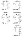
- FIGS. 4A and 4Billustrate the loss of efficiency due to charge sharing.
- FIGS. 5A-Cintroduce a pre-charge phase into the process shown in FIGS. 4A and 4B .
- FIGS. 6A-Dare a schematic illustration of the operation of the charge pump design of FIGS. 2A and 2B with pre-charging phases included.
- FIG. 7is a schematic for implementing a 2 -stage version for the arrangement of FIGS. 2A and 2B .
- FIG. 8is a schematic for implementing pre-charging in the charge pump of FIG. 7 .
- FIGS. 9A and 9Bare a schematic illustrations of the operation of one variety of charge pump design of the voltage adder type using a 4-phase clock.
- Non-volatile memory devicesoften operate on fairly low supply voltage values, but require higher voltage levels for the writing and erasing of data.
- the techniques presented herecan be advantageously used is such non-volatile memory devices, including the EEPROM based flash memory such as those described in U.S. Pat. Nos. 5,570,315, 5,903,495, 6,046,935 or the sort of “3D” structure presented in U.S. Pat. No. 7,696,812 and references found therein.
- FIGS. 2A and 2B and FIGS. 3A and 3BTwo specific designs are shown in FIGS. 2A and 2B and FIGS. 3A and 3B .
- FIGS. 2A and 2Bare a schematic illustration of the operation of one variety of charge pump design of the voltage adder type.
- the pumpincludes multiple (here 3) stages, each with a capacitor, that alternately operations in a reset phase and a charging phase.
- each of capacitors C 1 101 , C 2 103 , and C 3 105has its bottom plate connected to ground (or more generally a lower voltage value) and its top plate connected to Vcc (or more generally a high voltage value).
- the output of this pump legis taken from the node out and is not connected to the stage capacitors during reset.
- a load capacitor Ceq 107is also connected between the out node and ground.
- the connectionsare switched as shown in FIG. 2B so that the capacitors are connected in series, with the top plate of each connected to the bottom plate of the next in the series, except for the first capacitor C 1 101 that has its bottom plate connected to Vcc and the last capacitor in the series (here C 3 105 ) has its top plate connected to the output node.
- the switching circuitryis not explicitly shown here to simplify the discussion, but see FIG. 7 discussed below.
- the pumpalternates between the two phases, recharging the capacitors during the reset and then supplying the boosted charge in the charging phase.
- FIGS. 3A and 3Brespectively show a schematic of a clock voltage doubler type charge pump and a corresponding timing diagram.
- the pumphas left and right legs each connected to receive from node A the stage's input voltage, here Vdd, and each having a corresponding capacitor 205 and 207 .
- the bottom plate of capacitors 205 and 207are respectively connected to receive the non-overlapping clock signals CLK 1 and CLK 2 and the top plates are respectively connected to the input voltage through a switch of NMOS transistor 201 and 203 .
- the gates of these transistorare cross-coupled to the other leg at an intermediate node between the top plate of the capacitor of the other leg and the corresponding transistor of the other leg.
- the output nodes of the left and right legsare respectively taken at the nodes B and C.
- the node Bis connectable to ground and the top plate of the capacitor 205 be a switch here composed of PMOS 213 and NMOS 215 whose gates are connected to the clock signal CLK 1 A, which is the inverse of CLKL
- the node Cis connectable to ground and the top plate of the capacitor 207 be a switch here composed of PMOS 209 and NMOS 211 whose gates are connected to the clock signal CLK 2 A, which is the inverse of CLK 2 .
- Each output nodeis then connected to a load capacitor, 231 and 233 for the left and right output nodes, respectively.
- FIG. 3Bshows an exemplary set of waveforms for the voltage double circuit of FIG. 3A .
- the two clock signals CLK 1 and CLK 2are non-overlapping so that when either one is high, the other is low.
- the switches for the output node connectionsare controller by the inverses of CLK 1 and CLK 2 , CLK 1 A and CLK 2 A respectively.
- the outputs at nodes B and Care respectively V 02 and V 20 . As shown, these outputs are (ideally) the clock signals doubled to 2Vdd.
- FIGS. 3A and 3B and FIGS. 2A and 2Bprovided some of the basics of the operation of these two designs, but does not go into further detail on issues such as regulation, multi-stage (including variable stage) operation, or other design issues. More information on these and other issues on charge pumps that can be applied to the embodiments described here can be found, for example, in “Charge Pump Circuit Design” by Pan and Samaddar, McGraw-Hill, 2006, or “Charge Pumps: An Overview”, Pylarinos and Rogers, Department of Electrical and Computer Engineering University of Toronto, available on the webpage “www.eecg.toronto.edu/ ⁇ kphang/ece1371/chargepumps.pdf.” Further information on various other charge pump aspects and designs can be found in U.S.
- the outputis twice the input voltage.
- each stageadds Vcc to the preceding stage.
- Vccthe top plates is at Vcc and bottom plate at ground.
- the bottom plate of C 1 101will be at Vcc, but its top plate will have charge sharing with the bottom plate of C 2 103 .
- FIGS. 4A and 4Bshows three capacitors all having the same exemplary value of 2 pF and the high voltage level is here taken as 5V. (Since this is a linear system, the superposition theorem can be applied to see only the effect of charge sharing while omitting the clocking effect.)
- capacitors Cb 303 and Cc 305are connected in series as shown, each with both of their plates at ground.
- the switch 307is open and the top plate of Ca 301 is at 5V and the bottom plate is at ground.
- FIG. 4Bshows the final condition in the charging phase when the switch 307 is closed. Both of nodes Na and Nb will be at 3.33V, while the node is Nc is only at 1.67V. Considering the case where Nc corresponds to the nodes of the pump of FIGS. 2A and 2B and Cc corresponds to the load capacitance Ceq 107 , this illustrates how charge sharing between the capacitances can dilute the pumps efficiency.
- V 02 and V 20are twice the input value, 2 Vdd; but due to parasitic loading and active load, the actual amplitude will be less.
- the stacking of capacitors in the sort of arrangement discussed above with respect to FIGS. 2A and 2Bare used in pump clock drivers to generate high amplitude pump clocks to drive stages.
- stacking capacitancesis bad for power efficiency since charge sharing occurs and the internal node voltages will be lower than expected. This section addresses this issue and improves the efficiency of the pump through a combination of clock controls and selective pre-charging. The idea can be illustrated with respect to FIGS. 5A-C .
- FIG. 5Ais an initial condition in a reset phase, corresponds to FIG. 4A and is similarly labeled.
- FIG. 5Bintroduces a pre-charge phase for Cb 303 .
- the pre-charge phasethe node Nb is charged to the high level of, here, 5V.
- both of nodes Na and Nbare at 5V and Nc is at 2.5V.
- the switch 307is closed and the situation is similar to in FIG. 4B , except that the voltage levels will be different due to the pre-charge phase.
- the levels on nodes Na and Nbis 5V and at node Nc is 2.5V.
- the node Ncis switched from 0V to 2.5V. This corresponding raises the voltage on Nc in the charging phase from 1.67V to 2.5V, improving its efficiency.
- This same principlecan be applied to improve clock driver efficiencies for other pump designs as well.
- FIGS. 6A-Dillustrates how the pre-charging scheme can be applied to the pump design of FIGS. 2A and 2B .
- an exemplary embodiment using two intermediate pre-charge phasesbut in other embodiments less than all of the available pre-charge phases could be used.
- the high voltage levelis again the on-chip high level of Vcc, but other values could be used.
- FIGS. 6A and 6Dcorrespond to FIGS. 2A and 2B and are similarly labeled, but the introduction of the intervening pre-charge stages improves the efficiency and results in a higher output voltage in the charging phase.
- FIG. 6Bshows “Phase 1 ”, a first pre-charge phase.
- Capacitors C 1 101 and C 2 103remain as in the reset phase, but C 3 105 now has its top plate connected to the output node and its bottom plate is pre-charged to Vcc.
- the top plate of the preceding capacitor in the series C 2 103has its top plate connected to the bottom plate of C 3 105 and its bottom plate set to Vcc for pre-charging.
- the charging phase (or “Phase 3 ”) of FIG. 6DC 1 101 and C 2 103 are connected in series, with the bottom plate of C 1 101 at Vcc, as in FIG. 2B .
- FIG. 7is a schematic for implementing the arrangement of FIGS. 2A and 2B , but for a 2 -stage version to keep exposition more manageable.
- the capacitors 701 and 703are arranged in series between Vcc at the bottom and the output node at the top, which is also connected to the load capacitance 705 .
- the clock signal CLK 2is low
- the transistors 731 , 733 , and 735are off and the series connections cut off.
- CLK 1is high (and CLK 2 low)
- the transistors 711 , 713 , 723 , and 725are on and the reset phase conditions set.
- FIG. 8is a schematic of an implement of a pre-charge phase into the 2-stage design of FIG. 7 .
- a switch 741has now been added, connected at a node between the two capacitances 701 and 703 and an added clock signal CLK 4 .
- CLK 4Rather than control all of 731 , 733 and 735 all by CLK 2 , these are now respectively controlled by CLK 2 , CLK 2 B, and CLK 2 A.
- CLK 1is again high, and all of CLK 4 , CLK 2 A, CLK 2 B, and CLK 2 are low.
- CLK 1is again low, and all of CLK 4 , CLK 2 A, CLK 2 B, and CLK 2 are high.
- the clock voltage doubler type of pumpsuch as that shown in FIG. 3A , can also seen improved efficiencies through charge sharing. This can be done by introducing a four-phase clocking scheme for clock doubler to improve power/area efficiency.
- the exemplary clock voltage doubler of FIG. 3Awill again be used for the discussion here, as shown in FIG. 9A , but the clock signals CLK 1 A and CLK 2 A supplied the switches have been replaced by CLK 1 B and CLK 2 B. Although only one stage is stage is shown, as before there may be one or more preceding stages and, rather than the output nodes of the stages' legs being directly attached to the load capacitances 231 , 233 , there may also be one or more subsequent stages.
- the switches by which these output nodes B and C are connectable to either ground or the top plate of the legs capacitanceis again formed of a PMOS ( 213 or 209 ) and an NMOS ( 215 or 211 ) and the clock signals CLK 1 B, CLK 2 B are considered asserted when high. What is changed is, however, by the introduction of a four phase clock is the nature of the signals CLK 1 B and CLK 2 B and their relationship to CLK 1 and CLKK 2 . This is illustrated with respect to FIG. 9B .
- CLK 1 and CLK 2are again non-overlapping clocks such that when either one is asserted (high), the other is low.
- CLK 1 Bin no longer just the inverter version of CLK 1 . Instead, the falling edge of CLK 1 B is now earlier than the rising edge of CLK 1 , the interval between these two events shown in FIG. 9B as T 1 .
- CLK 1 Bis then low while CLK 2 is still high, this turns off NMOS 215 , turns 213 on, and allows the node B to be pre-charged to Vdd through 201 . This again reduces the amount of charge dilution, increasing the output.
- the node Ccan be pre-charged by de-asserting CLK 2 B before CLK 2 goes high.
- Power consumptioncan also reduced by changing the timing for when CLK 1 B and CLK 2 B are reasserted. If CLK 1 has its falling edge earlier than the rising edge of CLK 1 B, as shown in the interval T 2 of FIG. 9B , this will allow a portion of the charge on node B (at the voltage V 02 ) to be recycled through the transistor 213 back to the top plate of the capacitor 205 in reset phase of V 02 . Similarly, if CLK 2 has its falling edge earlier than the rising edge of CLK 2 B, this will allow a portion of the charge on node C (at the voltage V 20 ) to be recycled back to the top plate of the capacitor 207 in reset phase of V 20 .
Landscapes
- Engineering & Computer Science (AREA)
- Power Engineering (AREA)
- Dc-Dc Converters (AREA)
Abstract
Description
Claims (10)
Priority Applications (5)
| Application Number | Priority Date | Filing Date | Title |
|---|---|---|---|
| US12/973,641US8294509B2 (en) | 2010-12-20 | 2010-12-20 | Charge pump systems with reduction in inefficiencies due to charge sharing between capacitances |
| PCT/US2011/062890WO2012087532A1 (en) | 2010-12-20 | 2011-12-01 | Charge pump systems with reduction in inefficiencies due to charge sharing between capacitances |
| CN201180061349.0ACN103270682B (en) | 2010-12-20 | 2011-12-01 | Due to the charge pump system of the shared poor efficiency minimizing of the electric charge between electric capacity |
| KR1020137017046AKR20140008324A (en) | 2010-12-20 | 2011-12-01 | Charge pump systems with reduction in inefficiencies due to charge sharing between capacitances |
| US13/625,128US8421524B2 (en) | 2010-12-20 | 2012-09-24 | Charge pump systems with reduction in inefficiencies due to charge sharing between capacitances |
Applications Claiming Priority (1)
| Application Number | Priority Date | Filing Date | Title |
|---|---|---|---|
| US12/973,641US8294509B2 (en) | 2010-12-20 | 2010-12-20 | Charge pump systems with reduction in inefficiencies due to charge sharing between capacitances |
Related Child Applications (1)
| Application Number | Title | Priority Date | Filing Date |
|---|---|---|---|
| US13/625,128DivisionUS8421524B2 (en) | 2010-12-20 | 2012-09-24 | Charge pump systems with reduction in inefficiencies due to charge sharing between capacitances |
Publications (2)
| Publication Number | Publication Date |
|---|---|
| US20120154023A1 US20120154023A1 (en) | 2012-06-21 |
| US8294509B2true US8294509B2 (en) | 2012-10-23 |
Family
ID=45346571
Family Applications (2)
| Application Number | Title | Priority Date | Filing Date |
|---|---|---|---|
| US12/973,641Expired - Fee RelatedUS8294509B2 (en) | 2010-12-20 | 2010-12-20 | Charge pump systems with reduction in inefficiencies due to charge sharing between capacitances |
| US13/625,128Expired - Fee RelatedUS8421524B2 (en) | 2010-12-20 | 2012-09-24 | Charge pump systems with reduction in inefficiencies due to charge sharing between capacitances |
Family Applications After (1)
| Application Number | Title | Priority Date | Filing Date |
|---|---|---|---|
| US13/625,128Expired - Fee RelatedUS8421524B2 (en) | 2010-12-20 | 2012-09-24 | Charge pump systems with reduction in inefficiencies due to charge sharing between capacitances |
Country Status (4)
| Country | Link |
|---|---|
| US (2) | US8294509B2 (en) |
| KR (1) | KR20140008324A (en) |
| CN (1) | CN103270682B (en) |
| WO (1) | WO2012087532A1 (en) |
Cited By (11)
| Publication number | Priority date | Publication date | Assignee | Title |
|---|---|---|---|---|
| US20110234652A1 (en)* | 2010-03-23 | 2011-09-29 | Samsung Electronics Co., Ltd. | Charge pump, a method for controlling the same, and a display driving system comprising the charge pump |
| US9164526B2 (en) | 2012-09-27 | 2015-10-20 | Sandisk Technologies Inc. | Sigma delta over-sampling charge pump analog-to-digital converter |
| US9330776B2 (en) | 2014-08-14 | 2016-05-03 | Sandisk Technologies Inc. | High voltage step down regulator with breakdown protection |
| US9520776B1 (en) | 2015-09-18 | 2016-12-13 | Sandisk Technologies Llc | Selective body bias for charge pump transfer switches |
| US9553506B1 (en) | 2015-10-15 | 2017-01-24 | Sandisk Technologies Llc | Charge pump strength calibration and screening in circuit design |
| US9647536B2 (en) | 2015-07-28 | 2017-05-09 | Sandisk Technologies Llc | High voltage generation using low voltage devices |
| US9698676B1 (en) | 2016-03-11 | 2017-07-04 | Sandisk Technologies Llc | Charge pump based over-sampling with uniform step size for current detection |
| US9810723B2 (en) | 2012-09-27 | 2017-11-07 | Sandisk Technologies Llc | Charge pump based over-sampling ADC for current detection |
| US9847063B2 (en) | 2013-11-04 | 2017-12-19 | Samsung Display Co., Ltd. | Liquid crystal display and driving method thereof |
| US9917507B2 (en) | 2015-05-28 | 2018-03-13 | Sandisk Technologies Llc | Dynamic clock period modulation scheme for variable charge pump load currents |
| US12348132B2 (en) | 2023-02-16 | 2025-07-01 | SanDisk Technologies, Inc. | Stage based frequency optimization for area reduction of charge pumps |
Families Citing this family (28)
| Publication number | Priority date | Publication date | Assignee | Title |
|---|---|---|---|---|
| WO2008086396A2 (en)* | 2007-01-09 | 2008-07-17 | Power Monitors Inc. | Method and apparatus for smart circuit breaker |
| US7969159B2 (en)* | 2007-07-25 | 2011-06-28 | Power Monitors, Inc. | Method and apparatus for an electrical conductor monitoring system |
| WO2009111386A2 (en)* | 2008-03-04 | 2009-09-11 | Power Monitors, Inc. | Method and apparatus for a voice-prompted electrical hookup |
| US8773108B2 (en) | 2009-11-10 | 2014-07-08 | Power Monitors, Inc. | System, method, and apparatus for a safe powerline communications instrumentation front-end |
| EP3324153A1 (en) | 2010-07-29 | 2018-05-23 | Power Monitors, Inc. | Method and apparatus for a demand management monitoring system |
| US10060957B2 (en) | 2010-07-29 | 2018-08-28 | Power Monitors, Inc. | Method and apparatus for a cloud-based power quality monitor |
| EP4318909A3 (en) | 2011-05-05 | 2024-03-06 | PSEMI Corporation | Dc-dc converter with modular stages |
| US10680515B2 (en) | 2011-05-05 | 2020-06-09 | Psemi Corporation | Power converters with modular stages |
| US9026063B2 (en)* | 2011-05-17 | 2015-05-05 | Triquint Semiconductor, Inc. | Complementary metal-oxide semiconductor direct current to direct current converter |
| US8743553B2 (en) | 2011-10-18 | 2014-06-03 | Arctic Sand Technologies, Inc. | Power converters with integrated capacitors |
| US8724353B1 (en) | 2013-03-15 | 2014-05-13 | Arctic Sand Technologies, Inc. | Efficient gate drivers for switched capacitor converters |
| US8619445B1 (en) | 2013-03-15 | 2013-12-31 | Arctic Sand Technologies, Inc. | Protection of switched capacitor power converter |
| DE112015001260T5 (en) | 2014-03-14 | 2016-12-08 | Arctic Sand Technologies, Inc. | Charge pump stability control |
| US10693368B2 (en) | 2014-03-14 | 2020-06-23 | Psemi Corporation | Charge pump stability control |
| KR102113002B1 (en) | 2014-04-07 | 2020-05-21 | 삼성전자주식회사 | Voltage doubler and nonvolatile memory device having the same |
| CN103986340B (en) | 2014-05-23 | 2017-10-10 | 台达电子企业管理(上海)有限公司 | Supply convertor |
| CN105634267A (en)* | 2014-11-07 | 2016-06-01 | 上海华虹集成电路有限责任公司 | Voltage bootstrap charge pump circuit used on low supply voltage condition |
| WO2016149063A1 (en) | 2015-03-13 | 2016-09-22 | Arctic Sand Technologies, Inc. | Dc-dc transformer with inductor for the facilitation of adiabatic inter-capacitor charge transport |
| WO2017007991A1 (en) | 2015-07-08 | 2017-01-12 | Arctic Sand Technologies, Inc. | Switched-capacitor power converters |
| WO2018031780A1 (en) | 2016-08-10 | 2018-02-15 | Kickstart International, Inc. | Modular multi stage pump assembly |
| CN106602864B (en)* | 2016-12-19 | 2018-10-30 | 中国科学院微电子研究所 | Clock voltage doubling circuit and charge pump |
| US10250133B2 (en)* | 2017-07-18 | 2019-04-02 | Stmicroelectronics International N.V. | Single-stage CMOS-based voltage quadrupler circuit |
| CN108809084B (en)* | 2018-06-14 | 2020-03-06 | 长江存储科技有限责任公司 | charge pump circuit |
| US10847227B2 (en)* | 2018-10-16 | 2020-11-24 | Silicon Storage Technology, Inc. | Charge pump for use in non-volatile flash memory devices |
| KR102491767B1 (en) | 2018-11-05 | 2023-01-27 | 삼성전자주식회사 | Electronic circuit including charge pump for converting voltage |
| CN110504831A (en)* | 2019-09-04 | 2019-11-26 | 长江存储科技有限责任公司 | A charge pump, charging and discharging method thereof, and storage device |
| CN115800728B (en)* | 2021-09-10 | 2024-08-20 | 圣邦微电子(北京)股份有限公司 | Clock charge pump circuit for configuring output voltage |
| KR20240050685A (en) | 2022-10-12 | 2024-04-19 | 삼성전자주식회사 | Charge pump having switch circuits for blocking leakage current during sudden power-off, and flash memory including the same |
Citations (170)
| Publication number | Priority date | Publication date | Assignee | Title |
|---|---|---|---|---|
| US3697860A (en) | 1971-03-15 | 1972-10-10 | Westinghouse Electric Corp | Dc static switch circuit with a main switch device and a power sharing circuit portion |
| US4271461A (en) | 1978-05-16 | 1981-06-02 | Siemens Aktiengesellschaft | Clock-controlled DC converter |
| US4511811A (en) | 1982-02-08 | 1985-04-16 | Seeq Technology, Inc. | Charge pump for providing programming voltage to the word lines in a semiconductor memory array |
| US4583157A (en) | 1985-02-08 | 1986-04-15 | At&T Bell Laboratories | Integrated circuit having a variably boosted node |
| US4636748A (en) | 1985-06-26 | 1987-01-13 | Data General Corporation | Charge pump for use in a phase-locked loop |
| US4736121A (en) | 1985-09-10 | 1988-04-05 | Sos Microelettronica S.p.A. | Charge pump circuit for driving N-channel MOS transistors |
| US4888738A (en) | 1988-06-29 | 1989-12-19 | Seeq Technology | Current-regulated, voltage-regulated erase circuit for EEPROM memory |
| US5140182A (en)* | 1989-06-09 | 1992-08-18 | Texas Instruments Incorporated | Plural stage voltage booster circuit with efficient electric charge transfer between successive stages |
| US5168174A (en) | 1991-07-12 | 1992-12-01 | Texas Instruments Incorporated | Negative-voltage charge pump with feedback control |
| US5175706A (en) | 1989-12-07 | 1992-12-29 | Sgs-Thomson Microelectronics S.A. | Programming voltage generator circuit for programmable memory |
| US5263000A (en) | 1992-10-22 | 1993-11-16 | Advanced Micro Devices, Inc. | Drain power supply |
| US5335198A (en) | 1993-05-06 | 1994-08-02 | Advanced Micro Devices, Inc. | Flash EEPROM array with high endurance |
| US5392205A (en) | 1991-11-07 | 1995-02-21 | Motorola, Inc. | Regulated charge pump and method therefor |
| US5436587A (en) | 1993-11-24 | 1995-07-25 | Sundisk Corporation | Charge pump circuit with exponetral multiplication |
| US5483434A (en) | 1992-01-14 | 1996-01-09 | Seesink; Petrus H. | High voltage generator having output current control |
| US5508971A (en) | 1994-10-17 | 1996-04-16 | Sandisk Corporation | Programmable power generation circuit for flash EEPROM memory systems |
| US5521547A (en) | 1992-06-24 | 1996-05-28 | Nec Corporation | Boost voltage generating circuit |
| US5563779A (en) | 1994-12-05 | 1996-10-08 | Motorola, Inc. | Method and apparatus for a regulated supply on an integrated circuit |
| US5570315A (en) | 1993-09-21 | 1996-10-29 | Kabushiki Kaisha Toshiba | Multi-state EEPROM having write-verify control circuit |
| US5596532A (en) | 1995-10-18 | 1997-01-21 | Sandisk Corporation | Flash EEPROM self-adaptive voltage generation circuit operative within a continuous voltage source range |
| US5602794A (en) | 1995-09-29 | 1997-02-11 | Intel Corporation | Variable stage charge pump |
| US5625544A (en) | 1996-04-25 | 1997-04-29 | Programmable Microelectronics Corp. | Charge pump |
| US5734286A (en) | 1993-05-19 | 1998-03-31 | Kabushiki Kaisha Toshiba | Driving device of charge pump circuit and driving pulse generation method thereof |
| US5801987A (en) | 1997-03-17 | 1998-09-01 | Motorola, Inc. | Automatic transition charge pump for nonvolatile memories |
| US5818766A (en) | 1997-03-05 | 1998-10-06 | Integrated Silicon Solution Inc. | Drain voltage pump circuit for nonvolatile memory device |
| US5828596A (en) | 1996-09-26 | 1998-10-27 | Sharp Kabushiki Kaisha | Semiconductor memory device |
| US5903495A (en) | 1996-03-18 | 1999-05-11 | Kabushiki Kaisha Toshiba | Semiconductor device and memory system |
| US5943226A (en) | 1997-02-27 | 1999-08-24 | Lg Semicon Co., Ltd. | Bootstrap charge pump circuit |
| US5945870A (en) | 1996-07-18 | 1999-08-31 | Altera Corporation | Voltage ramp rate control circuit |
| US5969565A (en) | 1996-05-17 | 1999-10-19 | Nec Corporation | Voltage booster circuit |
| US5973546A (en) | 1996-06-27 | 1999-10-26 | Advanced Micro Devices, Inc. | Charge pump circuit architecture |
| US5982222A (en) | 1995-12-30 | 1999-11-09 | Samsung Electronics, Co., Ltd. | High voltage generating circuit for a semiconductor memory device |
| US6008690A (en) | 1997-06-11 | 1999-12-28 | Nec Corporation | Booster circuit |
| US6018264A (en) | 1998-02-11 | 2000-01-25 | Lg Semicon Co., Ltd. | Pumping circuit with amplitude limited to prevent an over pumping for semiconductor device |
| US6023187A (en) | 1997-12-23 | 2000-02-08 | Mitsubishi Semiconductor America, Inc. | Voltage pump for integrated circuit and operating method thereof |
| US6026002A (en) | 1996-03-28 | 2000-02-15 | Siemens Aktiengesellschaft | Circuit configuration for supplying an electronic load circuit |
| US6104225A (en) | 1997-04-21 | 2000-08-15 | Fujitsu Limited | Semiconductor device using complementary clock and signal input state detection circuit used for the same |
| US6107862A (en) | 1997-02-28 | 2000-08-22 | Seiko Instruments Inc. | Charge pump circuit |
| US6134145A (en) | 1998-06-23 | 2000-10-17 | Sandisk Corporation | High data rate write process for non-volatile flash memories |
| US6151229A (en) | 1999-06-30 | 2000-11-21 | Intel Corporation | Charge pump with gated pumped output diode at intermediate stage |
| US6154088A (en) | 1996-07-18 | 2000-11-28 | Micron Technology, Inc. | Clocking scheme and charge transfer switch for increasing the efficiency of a charge pump or other circuit |
| WO2001006336A1 (en) | 1999-07-15 | 2001-01-25 | Maxim Integrated Products, Inc. | Pulse frequency operation of regulated charge pumps |
| US6188590B1 (en) | 1996-12-18 | 2001-02-13 | Macronix International Co., Ltd. | Regulator system for charge pump circuits |
| US6198645B1 (en) | 1998-07-02 | 2001-03-06 | National Semiconductor Corporation | Buck and boost switched capacitor gain stage with optional shared rest state |
| US6208198B1 (en) | 1998-10-27 | 2001-03-27 | Hyundai Electronics Industries Co., Ltd. | Drain voltage pumping circuit |
| US6249898B1 (en) | 1998-06-30 | 2001-06-19 | Synopsys, Inc. | Method and system for reliability analysis of CMOS VLSI circuits based on stage partitioning and node activities |
| US6249445B1 (en) | 1999-02-15 | 2001-06-19 | Nec Corporation | Booster including charge pumping circuit with its electric power consumption reduced and method of operating the same |
| US6285622B1 (en) | 1999-10-29 | 2001-09-04 | Mitsubishi Denki Kabushiki Kaisha | Semiconductor device |
| US6297687B1 (en) | 1998-08-11 | 2001-10-02 | Oki Electric Industry Co., Ltd. | Drive control circuit of charged pump circuit |
| US6314025B1 (en) | 1998-06-23 | 2001-11-06 | Sandisk Corporation | High data rate write process for non-volatile flash memories |
| US6320796B1 (en) | 2000-11-10 | 2001-11-20 | Marvell International, Ltd. | Variable slope charge pump control |
| US6320428B1 (en) | 1997-02-26 | 2001-11-20 | Kabushiki Kaisha Toshiba | Semiconductor integrated circuit device |
| US6329869B1 (en) | 1999-05-19 | 2001-12-11 | Nec Corporation | Semiconductor device with less influence of noise |
| US20020008566A1 (en) | 2000-07-18 | 2002-01-24 | Mitsubishi Denki Kabushiki Kaisha And Mitsubishi Electric Engineering Company Limited | Internal Voltage generation circuit |
| US6344984B1 (en) | 1999-09-03 | 2002-02-05 | Nec Corporation | Voltage multiplier having an intermediate tap |
| US6344959B1 (en) | 1998-05-01 | 2002-02-05 | Unitrode Corporation | Method for sensing the output voltage of a charge pump circuit without applying a load to the output stage |
| US20020014908A1 (en) | 1998-12-21 | 2002-02-07 | Christl Lauterbach | Device for voltage multiplication with high efficiency, combination of the device with a battery-operated apparatus, and low-power loss generation of a programming voltage |
| US6359798B1 (en) | 2000-12-08 | 2002-03-19 | Samsung Electronics Co., Ltd. | Charge pump voltage converter |
| US6370075B1 (en) | 1998-06-30 | 2002-04-09 | Sandisk Corporation | Charge pump circuit adjustable in response to an external voltage source |
| US6369642B1 (en) | 2000-12-26 | 2002-04-09 | Intel Corporation | Output switch for charge pump reconfiguration |
| US6400202B1 (en) | 2000-02-10 | 2002-06-04 | International Business Machines Corporation | Programmable delay element and synchronous DRAM using the same |
| US6404274B1 (en) | 1998-04-09 | 2002-06-11 | Kabushiki Kaisha Toshiba | Internal voltage generating circuit capable of generating variable multi-level voltages |
| US20020075706A1 (en) | 1990-04-06 | 2002-06-20 | Mosaid Technologies Incorporated | Boosted voltage supply |
| US6424570B1 (en) | 2001-06-26 | 2002-07-23 | Advanced Micro Devices, Inc. | Modulated charge pump with uses an analog to digital converter to compensate for supply voltage variations |
| US6445243B2 (en) | 2000-05-10 | 2002-09-03 | Sanyo Electric Co., Ltd. | Charge-pump circuit and control method thereof |
| US20020130701A1 (en) | 2001-03-16 | 2002-09-19 | Matrix Semiconductor, Inc. | Multi-stage charge pump |
| US6456170B1 (en) | 1999-06-01 | 2002-09-24 | Fujitsu Limited | Comparator and voltage controlled oscillator circuit |
| US20020140463A1 (en) | 2001-03-15 | 2002-10-03 | Paul Cheung | Programmable soft-start control for charge pump |
| US6476666B1 (en) | 2001-05-30 | 2002-11-05 | Alliance Semiconductor Corporation | Bootstrapped charge pump |
| US6518830B2 (en) | 2000-08-22 | 2003-02-11 | Stmicroelectronics S.R.L. | High efficiency electronic circuit for generating and regulating a supply voltage |
| US6525614B2 (en) | 2000-11-17 | 2003-02-25 | Sanyo Electric Co., Ltd. | Voltage boost system having feedback control |
| US6525949B1 (en) | 2000-12-22 | 2003-02-25 | Matrix Semiconductor, Inc. | Charge pump circuit |
| US6531792B2 (en) | 2001-04-10 | 2003-03-11 | Fujitsu Limited | DC-DC converter and storage apparatus |
| US6538930B2 (en) | 2001-01-09 | 2003-03-25 | Mitsubishi Denki Kabushiki Kaisha | Charge pump circuit for generating positive and negative voltage with reverse current prevention circuit and a nonvolatile memory using the same |
| US6545529B2 (en) | 2000-05-02 | 2003-04-08 | Hynix Semiconductor Inc. | High voltage generating circuit |
| US6577535B2 (en) | 2001-02-16 | 2003-06-10 | Sandisk Corporation | Method and system for distributed power generation in multi-chip memory systems |
| US20030128560A1 (en) | 2002-01-10 | 2003-07-10 | Saiki William John | High voltage generation and regulation system for digital multilevel nonvolatile memory |
| US6606267B2 (en) | 1998-06-23 | 2003-08-12 | Sandisk Corporation | High data rate write process for non-volatile flash memories |
| US20030214346A1 (en) | 2002-02-25 | 2003-11-20 | Stmicroelectronics S.R.I. | Charge pump for negative voltages |
| US20040046603A1 (en) | 2002-09-06 | 2004-03-11 | Lorenzo Bedarida | Modular charge pump architecture |
| US6724241B1 (en) | 2002-10-25 | 2004-04-20 | Atmel Corporation | Variable charge pump circuit with dynamic load |
| US6734718B1 (en) | 2002-12-23 | 2004-05-11 | Sandisk Corporation | High voltage ripple reduction |
| US6781440B2 (en) | 2002-02-18 | 2004-08-24 | Winbond Electronics Corp. | Charge pump circuit with voltage multiplier for boosting clock signal and method thereof |
| US6798274B2 (en) | 2002-03-27 | 2004-09-28 | Sanyo Electric Co., Ltd. | Booster and imaging device using booster |
| US6834001B2 (en) | 2001-09-26 | 2004-12-21 | Sanyo Electric Co., Ltd. | Multi-stage switched capacitor DC-DC converter |
| US6859091B1 (en) | 2003-09-18 | 2005-02-22 | Maxim Integrated Products, Inc. | Continuous linear regulated zero dropout charge pump with high efficiency load predictive clocking scheme |
| US6878981B2 (en) | 2003-03-20 | 2005-04-12 | Tower Semiconductor Ltd. | Triple-well charge pump stage with no threshold voltage back-bias effect |
| US20050093614A1 (en) | 2003-10-30 | 2005-05-05 | Dong-Uk Lee | Multi stage voltage pump circuit |
| US6891764B2 (en) | 2003-04-11 | 2005-05-10 | Intel Corporation | Apparatus and method to read a nonvolatile memory |
| US6894554B2 (en) | 2002-01-17 | 2005-05-17 | Seiko Epson Corporation | Step-up circuits |
| US6922096B2 (en) | 2003-08-07 | 2005-07-26 | Sandisk Corporation | Area efficient charge pump |
| US6927441B2 (en) | 2001-03-20 | 2005-08-09 | Stmicroelectronics S.R.L. | Variable stage charge pump |
| US6933768B2 (en)* | 2002-06-20 | 2005-08-23 | Infineon Technologies Ag | Method for increasing the input voltage of an integrated circuit with a two-stage charge pump, and integrated circuit |
| US20050195017A1 (en) | 2004-03-03 | 2005-09-08 | Tien-Tzu Chen | High efficiency charge pump with prevention from reverse current |
| US20050248386A1 (en) | 2004-05-10 | 2005-11-10 | Sandisk Corporation | Four phase charge pump operable without phase overlap with improved efficiency |
| US6975135B1 (en) | 2002-12-10 | 2005-12-13 | Altera Corporation | Universally programmable output buffer |
| US6990031B2 (en) | 2001-09-03 | 2006-01-24 | Elpida Memory, Inc. | Semiconductor memory device control method and semiconductor memory device |
| US7002381B1 (en) | 2001-12-11 | 2006-02-21 | Advanced Micro Devices, Inc. | Switched-capacitor controller to control the rise times of on-chip generated high voltages |
| US7023260B2 (en) | 2003-06-30 | 2006-04-04 | Matrix Semiconductor, Inc. | Charge pump circuit incorporating corresponding parallel charge pump stages and method therefor |
| US20060098505A1 (en) | 2004-11-04 | 2006-05-11 | Chih-Hung Cho | Failure test method for split gate flash memory |
| US20060114053A1 (en) | 2004-11-30 | 2006-06-01 | Renesas Technology Corp. | Charge-pump-type power supply circuit |
| US7116154B2 (en) | 2003-08-06 | 2006-10-03 | Spansion Llc | Low power charge pump |
| US7120051B2 (en) | 2004-12-14 | 2006-10-10 | Sandisk Corporation | Pipelined programming of non-volatile memories using early data |
| US7129759B2 (en) | 2004-02-03 | 2006-10-31 | Nec Electronics Corporation | Integrated circuit including an overvoltage protection circuit |
| US20060244518A1 (en) | 2005-04-29 | 2006-11-02 | Hynix Semiconductor Inc. | Internal voltage generator |
| US20060250177A1 (en) | 2005-05-09 | 2006-11-09 | Thorp Tyler J | Methods and apparatus for dynamically reconfiguring a charge pump during output transients |
| US7135911B2 (en) | 2000-05-24 | 2006-11-14 | Kabushiki Kaisha Toshiba | Potential detector and semiconductor integrated circuit |
| US7135910B2 (en) | 2002-09-27 | 2006-11-14 | Sandisk Corporation | Charge pump with fibonacci number multiplication |
| US20070001745A1 (en) | 2005-06-29 | 2007-01-04 | Chih-Jen Yen | Charge pump for generating arbitrary voltage levels |
| JP2007020268A (en) | 2005-07-06 | 2007-01-25 | Casio Comput Co Ltd | Power circuit |
| US20070053216A1 (en) | 2005-09-02 | 2007-03-08 | Texas Instruments Incorporated | Three-phase low noise charge pump and method |
| US20070069805A1 (en) | 2005-09-29 | 2007-03-29 | Hynix Semiconductor Inc. | Internal voltage generating circuit |
| US7208996B2 (en) | 2004-03-26 | 2007-04-24 | Sanyo Electric Co., Ltd. | Charge pump circuit |
| US7224591B2 (en) | 2005-02-24 | 2007-05-29 | Sharp Kabushiki Kaisha | Charge pump DC/DC converter circuit |
| US7227780B2 (en) | 2004-11-30 | 2007-06-05 | Spansion Llc | Semiconductor device and control method thereof |
| US20070126494A1 (en) | 2005-12-06 | 2007-06-07 | Sandisk Corporation | Charge pump having shunt diode for improved operating efficiency |
| US20070139099A1 (en) | 2005-12-16 | 2007-06-21 | Sandisk Corporation | Charge pump regulation control for improved power efficiency |
| US20070139100A1 (en) | 2005-12-16 | 2007-06-21 | Sandisk Corporation | Voltage regulation with active supplemental current for output stabilization |
| US7239192B2 (en) | 2003-08-06 | 2007-07-03 | Stmicroelectronics Sa | Self-reparable device to generate a high voltage, and method for repairing a device to generate a high voltage |
| US7253676B2 (en) | 2003-12-25 | 2007-08-07 | Kabushiki Kaisha Toshiba | Semiconductor device and driving method of semiconductor device |
| US7259612B2 (en) | 2005-06-28 | 2007-08-21 | Atmel Corporation | Efficient charge pump for a wide range of supply voltages |
| US20070211502A1 (en) | 2006-03-07 | 2007-09-13 | Kunihiro Komiya | Voltage step-up circuit and electric appliance therewith |
| US20070222498A1 (en) | 2006-03-24 | 2007-09-27 | Freescale Semiconductor Inc. | Slew rate control of a charge pump |
| US7276960B2 (en) | 2005-07-18 | 2007-10-02 | Dialog Semiconductor Gmbh | Voltage regulated charge pump with regulated charge current into the flying capacitor |
| US20070229149A1 (en) | 2006-03-30 | 2007-10-04 | Sandisk Corporation | Voltage regulator having high voltage protection |
| US20080012627A1 (en) | 2006-07-13 | 2008-01-17 | Yosuke Kato | System and method for low voltage booster circuits |
| US20080024096A1 (en) | 2006-07-31 | 2008-01-31 | Sandisk Corporation | Hybrid charge pump regulation |
| US20080042731A1 (en) | 2005-06-03 | 2008-02-21 | Atmel Corporation | High efficiency bi-directional charge pump circuit |
| US7368979B2 (en) | 2006-09-19 | 2008-05-06 | Sandisk Corporation | Implementation of output floating scheme for hv charge pumps |
| US20080111604A1 (en) | 2005-03-17 | 2008-05-15 | Boerstler David W | Digital circuit to measure and/or correct duty cycles |
| US20080116963A1 (en) | 2006-11-20 | 2008-05-22 | Hynix Semiconductor Inc. | Clock control circuit and voltage pumping device using the same |
| DE102007026290A1 (en) | 2006-12-28 | 2008-07-03 | Samsung Electronics Co., Ltd., Suwon | High voltage generating circuit, has regulator generating high voltage measuring current for measuring high voltage depending on level of high voltage, for controlling control signal, and for generating activation signal |
| US20080157852A1 (en) | 2006-12-29 | 2008-07-03 | Sandisk Corporation | Unified voltage generation apparatus with improved power efficiency |
| US20080157859A1 (en) | 2006-12-29 | 2008-07-03 | Sandisk Corporation | Unified voltage generation method with improved power efficiency |
| US7397677B1 (en) | 2006-02-08 | 2008-07-08 | National Semiconductor Corporation | Apparatus and method for charge pump control with adjustable series resistance |
| US20080218134A1 (en) | 2007-03-08 | 2008-09-11 | Matsushita Electric Industrial Co., Ltd. | Power supply apparatus |
| US20080239856A1 (en) | 2007-03-30 | 2008-10-02 | Tyler Thorp | Method for Load-Based Voltage Generation |
| US20080239802A1 (en) | 2007-03-30 | 2008-10-02 | Tyler Thorp | Device with Load-Based Voltage Generation |
| US7436241B2 (en) | 2006-10-31 | 2008-10-14 | Au Optronics Corp. | Charge pump |
| US20080278222A1 (en) | 2006-07-19 | 2008-11-13 | Stmicroelectronics S.R.I. | Charge pump circuit |
| US20080307342A1 (en) | 2007-06-08 | 2008-12-11 | Apple Inc. | Rendering Semi-Transparent User Interface Elements |
| US7468628B2 (en) | 2004-11-08 | 2008-12-23 | Hynix Semiconductor Inc. | Internal voltage generators for semiconductor memory device |
| US20090033306A1 (en) | 2007-08-02 | 2009-02-05 | Toru Tanzawa | Voltage trimming |
| US7495500B2 (en) | 2006-12-31 | 2009-02-24 | Sandisk 3D Llc | Method for using a multiple polarity reversible charge pump circuit |
| US20090051413A1 (en) | 2007-08-20 | 2009-02-26 | Taiwan Semiconductor Manufacturing Company, Ltd. | Apparatus and method for increasing charge pump efficiency |
| US20090058507A1 (en) | 2007-08-28 | 2009-03-05 | Prajit Nandi | Bottom Plate Regulated Charge Pump |
| US20090063918A1 (en) | 2007-08-27 | 2009-03-05 | Macronix International Co., Ltd. | Apparatus and method for detecting word line leakage in memory devices |
| US20090058506A1 (en) | 2007-08-28 | 2009-03-05 | Prajit Nandi | Bottom Plate Regulation of Charge Pumps |
| US20090091366A1 (en) | 2007-10-09 | 2009-04-09 | Hynix Semiconductor, Inc. | Voltage generator of semiconductor integrated circuit |
| US20090121780A1 (en) | 2007-11-12 | 2009-05-14 | Macronix International Co., Ltd. | Multiple-stage charge pump with charge recycle circuit |
| US20090153232A1 (en) | 2007-05-25 | 2009-06-18 | Atmel Corporation | Low voltage charge pump |
| US20090153230A1 (en) | 2007-12-12 | 2009-06-18 | Feng Pan | Low Voltage Charge Pump with Regulation |
| US20090153231A1 (en) | 2007-12-12 | 2009-06-18 | Feng Pan | Diode Connected Regulation of Charge Pumps |
| US20090167418A1 (en) | 2007-10-24 | 2009-07-02 | Vijay Raghavan | Supply Regulated Charge Pump System |
| US20090174441A1 (en) | 2008-01-08 | 2009-07-09 | Gebara Fadi H | Peak Power Reduction Methods in Distributed Charge Pump Systems |
| US7579903B2 (en) | 2005-08-03 | 2009-08-25 | Nec Electronics Corporation | Power-source potential control circuit and method of trimming power-source potential |
| US20090296488A1 (en) | 2008-05-28 | 2009-12-03 | Hao Thai Nguyen | High Speed Sense Amplifier Array and Method for Nonvolatile Memory |
| US20090315616A1 (en) | 2008-06-24 | 2009-12-24 | Qui Vi Nguyen | Clock Generator Circuit for a Charge Pump |
| US20090322413A1 (en) | 2008-06-25 | 2009-12-31 | Huynh Jonathan H | Techniques of Ripple Reduction for Charge Pumps |
| US20100019832A1 (en) | 2008-06-09 | 2010-01-28 | Feng Pan | Self-Adaptive Multi-Stage Charge Pump |
| US7671572B2 (en) | 2006-04-07 | 2010-03-02 | Samsung Electronics Co. Ltd. | Voltage boost circuit and voltage boosting method using voltage boost clock signal with varying frequency |
| US20100074034A1 (en) | 2008-09-23 | 2010-03-25 | Marco Cazzaniga | Voltage regulator with reduced sensitivity of output voltage to change in load current |
| US20100085794A1 (en) | 2008-10-06 | 2010-04-08 | Yingchang Chen | Set and reset detection circuits for reversible resistance switching memory material |
| US7696812B2 (en) | 2006-12-31 | 2010-04-13 | Sandisk 3D Llc | Cooperative charge pump circuit and method |
| US7795952B2 (en) | 2008-12-17 | 2010-09-14 | Sandisk Corporation | Regulation of recovery rates in charge pumps |
| US20100244935A1 (en) | 2007-11-05 | 2010-09-30 | Electronics And Telecommunications Research Institute | High-voltage cmos charge pump |
| US7956673B2 (en) | 2008-08-11 | 2011-06-07 | Micron Technology, Inc. | Variable stage charge pump and method for providing boosted output voltage |
| US20110133820A1 (en) | 2009-12-09 | 2011-06-09 | Feng Pan | Multi-Stage Charge Pump with Variable Number of Boosting Stages |
| US20110148509A1 (en) | 2009-12-17 | 2011-06-23 | Feng Pan | Techniques to Reduce Charge Pump Overshoot |
| US7973592B2 (en) | 2009-07-21 | 2011-07-05 | Sandisk Corporation | Charge pump with current based regulation |
Family Cites Families (7)
| Publication number | Priority date | Publication date | Assignee | Title |
|---|---|---|---|---|
| KR100744640B1 (en) | 2005-11-02 | 2007-08-01 | 주식회사 하이닉스반도체 | Clock driver |
| US7579902B2 (en) | 2006-12-11 | 2009-08-25 | Atmel Corporation | Charge pump for generation of multiple output-voltage levels |
| JP4969322B2 (en)* | 2007-06-01 | 2012-07-04 | 三菱電機株式会社 | Voltage generating circuit and image display device including the same |
| US7602233B2 (en) | 2008-02-29 | 2009-10-13 | Freescale Semiconductor, Inc. | Voltage multiplier with improved efficiency |
| US8093953B2 (en) | 2009-03-20 | 2012-01-10 | Analog Devices, Inc. | Amplifier system with digital adaptive power boost |
| TWI397248B (en) | 2009-06-22 | 2013-05-21 | Richtek Technology Corp | Multi-input charge pump, and control circuit and operation method thereof |
| CN101902059B (en)* | 2010-07-20 | 2012-07-04 | 杭州硅星科技有限公司 | Method for capacitive load charging |
- 2010
- 2010-12-20USUS12/973,641patent/US8294509B2/ennot_activeExpired - Fee Related
- 2011
- 2011-12-01CNCN201180061349.0Apatent/CN103270682B/enactiveActive
- 2011-12-01WOPCT/US2011/062890patent/WO2012087532A1/enactiveApplication Filing
- 2011-12-01KRKR1020137017046Apatent/KR20140008324A/ennot_activeWithdrawn
- 2012
- 2012-09-24USUS13/625,128patent/US8421524B2/ennot_activeExpired - Fee Related
Patent Citations (195)
| Publication number | Priority date | Publication date | Assignee | Title |
|---|---|---|---|---|
| US3697860A (en) | 1971-03-15 | 1972-10-10 | Westinghouse Electric Corp | Dc static switch circuit with a main switch device and a power sharing circuit portion |
| US4271461A (en) | 1978-05-16 | 1981-06-02 | Siemens Aktiengesellschaft | Clock-controlled DC converter |
| US4511811A (en) | 1982-02-08 | 1985-04-16 | Seeq Technology, Inc. | Charge pump for providing programming voltage to the word lines in a semiconductor memory array |
| US4583157A (en) | 1985-02-08 | 1986-04-15 | At&T Bell Laboratories | Integrated circuit having a variably boosted node |
| US4636748A (en) | 1985-06-26 | 1987-01-13 | Data General Corporation | Charge pump for use in a phase-locked loop |
| US4736121A (en) | 1985-09-10 | 1988-04-05 | Sos Microelettronica S.p.A. | Charge pump circuit for driving N-channel MOS transistors |
| US4888738A (en) | 1988-06-29 | 1989-12-19 | Seeq Technology | Current-regulated, voltage-regulated erase circuit for EEPROM memory |
| US5140182A (en)* | 1989-06-09 | 1992-08-18 | Texas Instruments Incorporated | Plural stage voltage booster circuit with efficient electric charge transfer between successive stages |
| US5175706A (en) | 1989-12-07 | 1992-12-29 | Sgs-Thomson Microelectronics S.A. | Programming voltage generator circuit for programmable memory |
| US20020075706A1 (en) | 1990-04-06 | 2002-06-20 | Mosaid Technologies Incorporated | Boosted voltage supply |
| US5168174A (en) | 1991-07-12 | 1992-12-01 | Texas Instruments Incorporated | Negative-voltage charge pump with feedback control |
| US5392205A (en) | 1991-11-07 | 1995-02-21 | Motorola, Inc. | Regulated charge pump and method therefor |
| US5483434A (en) | 1992-01-14 | 1996-01-09 | Seesink; Petrus H. | High voltage generator having output current control |
| US5521547A (en) | 1992-06-24 | 1996-05-28 | Nec Corporation | Boost voltage generating circuit |
| US5263000A (en) | 1992-10-22 | 1993-11-16 | Advanced Micro Devices, Inc. | Drain power supply |
| US5335198A (en) | 1993-05-06 | 1994-08-02 | Advanced Micro Devices, Inc. | Flash EEPROM array with high endurance |
| US5734286A (en) | 1993-05-19 | 1998-03-31 | Kabushiki Kaisha Toshiba | Driving device of charge pump circuit and driving pulse generation method thereof |
| US5570315A (en) | 1993-09-21 | 1996-10-29 | Kabushiki Kaisha Toshiba | Multi-state EEPROM having write-verify control circuit |
| US5436587A (en) | 1993-11-24 | 1995-07-25 | Sundisk Corporation | Charge pump circuit with exponetral multiplication |
| US5592420A (en) | 1994-10-17 | 1997-01-07 | Sandisk Corporation | Programmable power generation circuit for flash EEPROM memory systems |
| US5568424A (en) | 1994-10-17 | 1996-10-22 | Sandisk Corporation | Programmable power generation circuit for flash EEPROM memory systems |
| US5693570A (en) | 1994-10-17 | 1997-12-02 | Sandisk Corporation | Process for manufacturing a programmable power generation circuit for flash EEPROM memory systems |
| US5563825A (en) | 1994-10-17 | 1996-10-08 | Sandisk Corporation | Programmable power generation circuit for flash eeprom memory systems |
| US5621685A (en) | 1994-10-17 | 1997-04-15 | Sandisk Corporation | Programmable power generation circuit for flash EEPROM memory systems |
| US5508971A (en) | 1994-10-17 | 1996-04-16 | Sandisk Corporation | Programmable power generation circuit for flash EEPROM memory systems |
| US5563779A (en) | 1994-12-05 | 1996-10-08 | Motorola, Inc. | Method and apparatus for a regulated supply on an integrated circuit |
| US5732039A (en) | 1995-09-29 | 1998-03-24 | Intel Corporation | Variable stage charge pump |
| US5767735A (en) | 1995-09-29 | 1998-06-16 | Intel Corporation | Variable stage charge pump |
| US5781473A (en) | 1995-09-29 | 1998-07-14 | Intel Corporation | Variable stage charge pump |
| US5602794A (en) | 1995-09-29 | 1997-02-11 | Intel Corporation | Variable stage charge pump |
| US5596532A (en) | 1995-10-18 | 1997-01-21 | Sandisk Corporation | Flash EEPROM self-adaptive voltage generation circuit operative within a continuous voltage source range |
| US5982222A (en) | 1995-12-30 | 1999-11-09 | Samsung Electronics, Co., Ltd. | High voltage generating circuit for a semiconductor memory device |
| US6046935A (en) | 1996-03-18 | 2000-04-04 | Kabushiki Kaisha Toshiba | Semiconductor device and memory system |
| US5903495A (en) | 1996-03-18 | 1999-05-11 | Kabushiki Kaisha Toshiba | Semiconductor device and memory system |
| US6026002A (en) | 1996-03-28 | 2000-02-15 | Siemens Aktiengesellschaft | Circuit configuration for supplying an electronic load circuit |
| US5625544A (en) | 1996-04-25 | 1997-04-29 | Programmable Microelectronics Corp. | Charge pump |
| US5969565A (en) | 1996-05-17 | 1999-10-19 | Nec Corporation | Voltage booster circuit |
| US5973546A (en) | 1996-06-27 | 1999-10-26 | Advanced Micro Devices, Inc. | Charge pump circuit architecture |
| US6307425B1 (en) | 1996-07-18 | 2001-10-23 | Micron Technology, Inc. | Clocking scheme and charge transfer switch for increasing the efficiency of a charge pump or other circuit |
| US5945870A (en) | 1996-07-18 | 1999-08-31 | Altera Corporation | Voltage ramp rate control circuit |
| US6154088A (en) | 1996-07-18 | 2000-11-28 | Micron Technology, Inc. | Clocking scheme and charge transfer switch for increasing the efficiency of a charge pump or other circuit |
| US5828596A (en) | 1996-09-26 | 1998-10-27 | Sharp Kabushiki Kaisha | Semiconductor memory device |
| US6188590B1 (en) | 1996-12-18 | 2001-02-13 | Macronix International Co., Ltd. | Regulator system for charge pump circuits |
| US6320428B1 (en) | 1997-02-26 | 2001-11-20 | Kabushiki Kaisha Toshiba | Semiconductor integrated circuit device |
| US5943226A (en) | 1997-02-27 | 1999-08-24 | Lg Semicon Co., Ltd. | Bootstrap charge pump circuit |
| US6107862A (en) | 1997-02-28 | 2000-08-22 | Seiko Instruments Inc. | Charge pump circuit |
| US5818766A (en) | 1997-03-05 | 1998-10-06 | Integrated Silicon Solution Inc. | Drain voltage pump circuit for nonvolatile memory device |
| US5801987A (en) | 1997-03-17 | 1998-09-01 | Motorola, Inc. | Automatic transition charge pump for nonvolatile memories |
| US6104225A (en) | 1997-04-21 | 2000-08-15 | Fujitsu Limited | Semiconductor device using complementary clock and signal input state detection circuit used for the same |
| US6008690A (en) | 1997-06-11 | 1999-12-28 | Nec Corporation | Booster circuit |
| US6023187A (en) | 1997-12-23 | 2000-02-08 | Mitsubishi Semiconductor America, Inc. | Voltage pump for integrated circuit and operating method thereof |
| US6018264A (en) | 1998-02-11 | 2000-01-25 | Lg Semicon Co., Ltd. | Pumping circuit with amplitude limited to prevent an over pumping for semiconductor device |
| US6404274B1 (en) | 1998-04-09 | 2002-06-11 | Kabushiki Kaisha Toshiba | Internal voltage generating circuit capable of generating variable multi-level voltages |
| US6344959B1 (en) | 1998-05-01 | 2002-02-05 | Unitrode Corporation | Method for sensing the output voltage of a charge pump circuit without applying a load to the output stage |
| US6944058B2 (en) | 1998-06-23 | 2005-09-13 | Sandisk Corporation | High data rate write process for non-volatile flash memories |
| US6134145A (en) | 1998-06-23 | 2000-10-17 | Sandisk Corporation | High data rate write process for non-volatile flash memories |
| US6314025B1 (en) | 1998-06-23 | 2001-11-06 | Sandisk Corporation | High data rate write process for non-volatile flash memories |
| US6606267B2 (en) | 1998-06-23 | 2003-08-12 | Sandisk Corporation | High data rate write process for non-volatile flash memories |
| US6249898B1 (en) | 1998-06-30 | 2001-06-19 | Synopsys, Inc. | Method and system for reliability analysis of CMOS VLSI circuits based on stage partitioning and node activities |
| US6556465B2 (en) | 1998-06-30 | 2003-04-29 | Sandisk Corporation | Adjustable circuits for analog or multi-level memory |
| US6370075B1 (en) | 1998-06-30 | 2002-04-09 | Sandisk Corporation | Charge pump circuit adjustable in response to an external voltage source |
| US6760262B2 (en) | 1998-06-30 | 2004-07-06 | Sandisk Corporation | Charge pump circuit adjustable in response to an external voltage source |
| US6198645B1 (en) | 1998-07-02 | 2001-03-06 | National Semiconductor Corporation | Buck and boost switched capacitor gain stage with optional shared rest state |
| US6297687B1 (en) | 1998-08-11 | 2001-10-02 | Oki Electric Industry Co., Ltd. | Drive control circuit of charged pump circuit |
| US6208198B1 (en) | 1998-10-27 | 2001-03-27 | Hyundai Electronics Industries Co., Ltd. | Drain voltage pumping circuit |
| US20020014908A1 (en) | 1998-12-21 | 2002-02-07 | Christl Lauterbach | Device for voltage multiplication with high efficiency, combination of the device with a battery-operated apparatus, and low-power loss generation of a programming voltage |
| US6249445B1 (en) | 1999-02-15 | 2001-06-19 | Nec Corporation | Booster including charge pumping circuit with its electric power consumption reduced and method of operating the same |
| US6329869B1 (en) | 1999-05-19 | 2001-12-11 | Nec Corporation | Semiconductor device with less influence of noise |
| US6456170B1 (en) | 1999-06-01 | 2002-09-24 | Fujitsu Limited | Comparator and voltage controlled oscillator circuit |
| US6151229A (en) | 1999-06-30 | 2000-11-21 | Intel Corporation | Charge pump with gated pumped output diode at intermediate stage |
| WO2001006336A1 (en) | 1999-07-15 | 2001-01-25 | Maxim Integrated Products, Inc. | Pulse frequency operation of regulated charge pumps |
| US6344984B1 (en) | 1999-09-03 | 2002-02-05 | Nec Corporation | Voltage multiplier having an intermediate tap |
| US6285622B1 (en) | 1999-10-29 | 2001-09-04 | Mitsubishi Denki Kabushiki Kaisha | Semiconductor device |
| US6400202B1 (en) | 2000-02-10 | 2002-06-04 | International Business Machines Corporation | Programmable delay element and synchronous DRAM using the same |
| US6545529B2 (en) | 2000-05-02 | 2003-04-08 | Hynix Semiconductor Inc. | High voltage generating circuit |
| US6445243B2 (en) | 2000-05-10 | 2002-09-03 | Sanyo Electric Co., Ltd. | Charge-pump circuit and control method thereof |
| US7135911B2 (en) | 2000-05-24 | 2006-11-14 | Kabushiki Kaisha Toshiba | Potential detector and semiconductor integrated circuit |
| US20020008566A1 (en) | 2000-07-18 | 2002-01-24 | Mitsubishi Denki Kabushiki Kaisha And Mitsubishi Electric Engineering Company Limited | Internal Voltage generation circuit |
| US6518830B2 (en) | 2000-08-22 | 2003-02-11 | Stmicroelectronics S.R.L. | High efficiency electronic circuit for generating and regulating a supply voltage |
| US6320796B1 (en) | 2000-11-10 | 2001-11-20 | Marvell International, Ltd. | Variable slope charge pump control |
| US6525614B2 (en) | 2000-11-17 | 2003-02-25 | Sanyo Electric Co., Ltd. | Voltage boost system having feedback control |
| US6359798B1 (en) | 2000-12-08 | 2002-03-19 | Samsung Electronics Co., Ltd. | Charge pump voltage converter |
| US6525949B1 (en) | 2000-12-22 | 2003-02-25 | Matrix Semiconductor, Inc. | Charge pump circuit |
| US6369642B1 (en) | 2000-12-26 | 2002-04-09 | Intel Corporation | Output switch for charge pump reconfiguration |
| US6538930B2 (en) | 2001-01-09 | 2003-03-25 | Mitsubishi Denki Kabushiki Kaisha | Charge pump circuit for generating positive and negative voltage with reverse current prevention circuit and a nonvolatile memory using the same |
| US6577535B2 (en) | 2001-02-16 | 2003-06-10 | Sandisk Corporation | Method and system for distributed power generation in multi-chip memory systems |
| US20020140463A1 (en) | 2001-03-15 | 2002-10-03 | Paul Cheung | Programmable soft-start control for charge pump |
| US6486728B2 (en) | 2001-03-16 | 2002-11-26 | Matrix Semiconductor, Inc. | Multi-stage charge pump |
| US20020130701A1 (en) | 2001-03-16 | 2002-09-19 | Matrix Semiconductor, Inc. | Multi-stage charge pump |
| US6927441B2 (en) | 2001-03-20 | 2005-08-09 | Stmicroelectronics S.R.L. | Variable stage charge pump |
| US6531792B2 (en) | 2001-04-10 | 2003-03-11 | Fujitsu Limited | DC-DC converter and storage apparatus |
| US6476666B1 (en) | 2001-05-30 | 2002-11-05 | Alliance Semiconductor Corporation | Bootstrapped charge pump |
| US6424570B1 (en) | 2001-06-26 | 2002-07-23 | Advanced Micro Devices, Inc. | Modulated charge pump with uses an analog to digital converter to compensate for supply voltage variations |
| US6990031B2 (en) | 2001-09-03 | 2006-01-24 | Elpida Memory, Inc. | Semiconductor memory device control method and semiconductor memory device |
| US6834001B2 (en) | 2001-09-26 | 2004-12-21 | Sanyo Electric Co., Ltd. | Multi-stage switched capacitor DC-DC converter |
| US7002381B1 (en) | 2001-12-11 | 2006-02-21 | Advanced Micro Devices, Inc. | Switched-capacitor controller to control the rise times of on-chip generated high voltages |
| US20030128560A1 (en) | 2002-01-10 | 2003-07-10 | Saiki William John | High voltage generation and regulation system for digital multilevel nonvolatile memory |
| US6894554B2 (en) | 2002-01-17 | 2005-05-17 | Seiko Epson Corporation | Step-up circuits |
| US6781440B2 (en) | 2002-02-18 | 2004-08-24 | Winbond Electronics Corp. | Charge pump circuit with voltage multiplier for boosting clock signal and method thereof |
| US6819162B2 (en) | 2002-02-25 | 2004-11-16 | Stmicroelectronics S.R.L. | Charge pump for negative voltages |
| US20030214346A1 (en) | 2002-02-25 | 2003-11-20 | Stmicroelectronics S.R.I. | Charge pump for negative voltages |
| US6798274B2 (en) | 2002-03-27 | 2004-09-28 | Sanyo Electric Co., Ltd. | Booster and imaging device using booster |
| US6933768B2 (en)* | 2002-06-20 | 2005-08-23 | Infineon Technologies Ag | Method for increasing the input voltage of an integrated circuit with a two-stage charge pump, and integrated circuit |
| US20040046603A1 (en) | 2002-09-06 | 2004-03-11 | Lorenzo Bedarida | Modular charge pump architecture |
| US7135910B2 (en) | 2002-09-27 | 2006-11-14 | Sandisk Corporation | Charge pump with fibonacci number multiplication |
| US6724241B1 (en) | 2002-10-25 | 2004-04-20 | Atmel Corporation | Variable charge pump circuit with dynamic load |
| US6975135B1 (en) | 2002-12-10 | 2005-12-13 | Altera Corporation | Universally programmable output buffer |
| US6734718B1 (en) | 2002-12-23 | 2004-05-11 | Sandisk Corporation | High voltage ripple reduction |
| US7116155B2 (en) | 2002-12-23 | 2006-10-03 | Sandisk Corporation | High voltage ripple reduction and substrate protection |
| US6878981B2 (en) | 2003-03-20 | 2005-04-12 | Tower Semiconductor Ltd. | Triple-well charge pump stage with no threshold voltage back-bias effect |
| US6891764B2 (en) | 2003-04-11 | 2005-05-10 | Intel Corporation | Apparatus and method to read a nonvolatile memory |
| US7023260B2 (en) | 2003-06-30 | 2006-04-04 | Matrix Semiconductor, Inc. | Charge pump circuit incorporating corresponding parallel charge pump stages and method therefor |
| US7116154B2 (en) | 2003-08-06 | 2006-10-03 | Spansion Llc | Low power charge pump |
| US7239192B2 (en) | 2003-08-06 | 2007-07-03 | Stmicroelectronics Sa | Self-reparable device to generate a high voltage, and method for repairing a device to generate a high voltage |
| US20050237103A1 (en) | 2003-08-07 | 2005-10-27 | Raul-Adrian Cernea | Area efficient charge pump |
| US6922096B2 (en) | 2003-08-07 | 2005-07-26 | Sandisk Corporation | Area efficient charge pump |
| US7113023B2 (en) | 2003-08-07 | 2006-09-26 | Sandisk Corporation | Area efficient charge pump |
| US6859091B1 (en) | 2003-09-18 | 2005-02-22 | Maxim Integrated Products, Inc. | Continuous linear regulated zero dropout charge pump with high efficiency load predictive clocking scheme |
| US20050093614A1 (en) | 2003-10-30 | 2005-05-05 | Dong-Uk Lee | Multi stage voltage pump circuit |
| US7253676B2 (en) | 2003-12-25 | 2007-08-07 | Kabushiki Kaisha Toshiba | Semiconductor device and driving method of semiconductor device |
| US7129759B2 (en) | 2004-02-03 | 2006-10-31 | Nec Electronics Corporation | Integrated circuit including an overvoltage protection circuit |
| US20050195017A1 (en) | 2004-03-03 | 2005-09-08 | Tien-Tzu Chen | High efficiency charge pump with prevention from reverse current |
| US6995603B2 (en) | 2004-03-03 | 2006-02-07 | Aimtron Technology Corp. | High efficiency charge pump with prevention from reverse current |
| US7208996B2 (en) | 2004-03-26 | 2007-04-24 | Sanyo Electric Co., Ltd. | Charge pump circuit |
| US7030683B2 (en) | 2004-05-10 | 2006-04-18 | Sandisk Corporation | Four phase charge pump operable without phase overlap with improved efficiency |
| US20050248386A1 (en) | 2004-05-10 | 2005-11-10 | Sandisk Corporation | Four phase charge pump operable without phase overlap with improved efficiency |
| US20060098505A1 (en) | 2004-11-04 | 2006-05-11 | Chih-Hung Cho | Failure test method for split gate flash memory |
| US7468628B2 (en) | 2004-11-08 | 2008-12-23 | Hynix Semiconductor Inc. | Internal voltage generators for semiconductor memory device |
| US20060114053A1 (en) | 2004-11-30 | 2006-06-01 | Renesas Technology Corp. | Charge-pump-type power supply circuit |
| US7227780B2 (en) | 2004-11-30 | 2007-06-05 | Spansion Llc | Semiconductor device and control method thereof |
| US7120051B2 (en) | 2004-12-14 | 2006-10-10 | Sandisk Corporation | Pipelined programming of non-volatile memories using early data |
| US7345928B2 (en) | 2004-12-14 | 2008-03-18 | Sandisk Corporation | Data recovery methods in multi-state memory after program fail |
| US7224591B2 (en) | 2005-02-24 | 2007-05-29 | Sharp Kabushiki Kaisha | Charge pump DC/DC converter circuit |
| US20080111604A1 (en) | 2005-03-17 | 2008-05-15 | Boerstler David W | Digital circuit to measure and/or correct duty cycles |
| US20060244518A1 (en) | 2005-04-29 | 2006-11-02 | Hynix Semiconductor Inc. | Internal voltage generator |
| US20060250177A1 (en) | 2005-05-09 | 2006-11-09 | Thorp Tyler J | Methods and apparatus for dynamically reconfiguring a charge pump during output transients |
| US20080042731A1 (en) | 2005-06-03 | 2008-02-21 | Atmel Corporation | High efficiency bi-directional charge pump circuit |
| US7259612B2 (en) | 2005-06-28 | 2007-08-21 | Atmel Corporation | Efficient charge pump for a wide range of supply voltages |
| US7279957B2 (en)* | 2005-06-29 | 2007-10-09 | Novatek Microelectronics Corp. | Charge pump for generating arbitrary voltage levels |
| US20070001745A1 (en) | 2005-06-29 | 2007-01-04 | Chih-Jen Yen | Charge pump for generating arbitrary voltage levels |
| JP2007020268A (en) | 2005-07-06 | 2007-01-25 | Casio Comput Co Ltd | Power circuit |
| US7276960B2 (en) | 2005-07-18 | 2007-10-02 | Dialog Semiconductor Gmbh | Voltage regulated charge pump with regulated charge current into the flying capacitor |
| US7579903B2 (en) | 2005-08-03 | 2009-08-25 | Nec Electronics Corporation | Power-source potential control circuit and method of trimming power-source potential |
| US20070053216A1 (en) | 2005-09-02 | 2007-03-08 | Texas Instruments Incorporated | Three-phase low noise charge pump and method |
| US20070069805A1 (en) | 2005-09-29 | 2007-03-29 | Hynix Semiconductor Inc. | Internal voltage generating circuit |
| US20070126494A1 (en) | 2005-12-06 | 2007-06-07 | Sandisk Corporation | Charge pump having shunt diode for improved operating efficiency |
| US20070139099A1 (en) | 2005-12-16 | 2007-06-21 | Sandisk Corporation | Charge pump regulation control for improved power efficiency |
| US20070139100A1 (en) | 2005-12-16 | 2007-06-21 | Sandisk Corporation | Voltage regulation with active supplemental current for output stabilization |
| US7397677B1 (en) | 2006-02-08 | 2008-07-08 | National Semiconductor Corporation | Apparatus and method for charge pump control with adjustable series resistance |
| US20070211502A1 (en) | 2006-03-07 | 2007-09-13 | Kunihiro Komiya | Voltage step-up circuit and electric appliance therewith |
| US20070222498A1 (en) | 2006-03-24 | 2007-09-27 | Freescale Semiconductor Inc. | Slew rate control of a charge pump |
| US20070229149A1 (en) | 2006-03-30 | 2007-10-04 | Sandisk Corporation | Voltage regulator having high voltage protection |
| US7671572B2 (en) | 2006-04-07 | 2010-03-02 | Samsung Electronics Co. Ltd. | Voltage boost circuit and voltage boosting method using voltage boost clock signal with varying frequency |
| US20080012627A1 (en) | 2006-07-13 | 2008-01-17 | Yosuke Kato | System and method for low voltage booster circuits |
| US20080278222A1 (en) | 2006-07-19 | 2008-11-13 | Stmicroelectronics S.R.I. | Charge pump circuit |
| US7554311B2 (en) | 2006-07-31 | 2009-06-30 | Sandisk Corporation | Hybrid charge pump regulation |
| US20080024096A1 (en) | 2006-07-31 | 2008-01-31 | Sandisk Corporation | Hybrid charge pump regulation |
| US7368979B2 (en) | 2006-09-19 | 2008-05-06 | Sandisk Corporation | Implementation of output floating scheme for hv charge pumps |
| US7436241B2 (en) | 2006-10-31 | 2008-10-14 | Au Optronics Corp. | Charge pump |
| US20080116963A1 (en) | 2006-11-20 | 2008-05-22 | Hynix Semiconductor Inc. | Clock control circuit and voltage pumping device using the same |
| US7772914B2 (en) | 2006-11-20 | 2010-08-10 | Hynix Semiconductor Inc. | Clock control circuit and voltage pumping device using the same |
| DE102007026290A1 (en) | 2006-12-28 | 2008-07-03 | Samsung Electronics Co., Ltd., Suwon | High voltage generating circuit, has regulator generating high voltage measuring current for measuring high voltage depending on level of high voltage, for controlling control signal, and for generating activation signal |
| US20080157859A1 (en) | 2006-12-29 | 2008-07-03 | Sandisk Corporation | Unified voltage generation method with improved power efficiency |
| US20080157852A1 (en) | 2006-12-29 | 2008-07-03 | Sandisk Corporation | Unified voltage generation apparatus with improved power efficiency |
| US7696812B2 (en) | 2006-12-31 | 2010-04-13 | Sandisk 3D Llc | Cooperative charge pump circuit and method |
| US7495500B2 (en) | 2006-12-31 | 2009-02-24 | Sandisk 3D Llc | Method for using a multiple polarity reversible charge pump circuit |
| US20080218134A1 (en) | 2007-03-08 | 2008-09-11 | Matsushita Electric Industrial Co., Ltd. | Power supply apparatus |
| US20080239802A1 (en) | 2007-03-30 | 2008-10-02 | Tyler Thorp | Device with Load-Based Voltage Generation |
| US20080239856A1 (en) | 2007-03-30 | 2008-10-02 | Tyler Thorp | Method for Load-Based Voltage Generation |
| US20090153232A1 (en) | 2007-05-25 | 2009-06-18 | Atmel Corporation | Low voltage charge pump |
| US20080307342A1 (en) | 2007-06-08 | 2008-12-11 | Apple Inc. | Rendering Semi-Transparent User Interface Elements |
| US20090033306A1 (en) | 2007-08-02 | 2009-02-05 | Toru Tanzawa | Voltage trimming |
| US20090051413A1 (en) | 2007-08-20 | 2009-02-26 | Taiwan Semiconductor Manufacturing Company, Ltd. | Apparatus and method for increasing charge pump efficiency |
| US20090063918A1 (en) | 2007-08-27 | 2009-03-05 | Macronix International Co., Ltd. | Apparatus and method for detecting word line leakage in memory devices |
| US20090058506A1 (en) | 2007-08-28 | 2009-03-05 | Prajit Nandi | Bottom Plate Regulation of Charge Pumps |
| US20090058507A1 (en) | 2007-08-28 | 2009-03-05 | Prajit Nandi | Bottom Plate Regulated Charge Pump |
| US20090091366A1 (en) | 2007-10-09 | 2009-04-09 | Hynix Semiconductor, Inc. | Voltage generator of semiconductor integrated circuit |
| US20090167418A1 (en) | 2007-10-24 | 2009-07-02 | Vijay Raghavan | Supply Regulated Charge Pump System |
| US20100244935A1 (en) | 2007-11-05 | 2010-09-30 | Electronics And Telecommunications Research Institute | High-voltage cmos charge pump |
| US20090121780A1 (en) | 2007-11-12 | 2009-05-14 | Macronix International Co., Ltd. | Multiple-stage charge pump with charge recycle circuit |
| US20090153231A1 (en) | 2007-12-12 | 2009-06-18 | Feng Pan | Diode Connected Regulation of Charge Pumps |
| US20090153230A1 (en) | 2007-12-12 | 2009-06-18 | Feng Pan | Low Voltage Charge Pump with Regulation |
| US20090174441A1 (en) | 2008-01-08 | 2009-07-09 | Gebara Fadi H | Peak Power Reduction Methods in Distributed Charge Pump Systems |
| US20090296488A1 (en) | 2008-05-28 | 2009-12-03 | Hao Thai Nguyen | High Speed Sense Amplifier Array and Method for Nonvolatile Memory |
| US20100019832A1 (en) | 2008-06-09 | 2010-01-28 | Feng Pan | Self-Adaptive Multi-Stage Charge Pump |
| US7969235B2 (en) | 2008-06-09 | 2011-06-28 | Sandisk Corporation | Self-adaptive multi-stage charge pump |
| US20090315616A1 (en) | 2008-06-24 | 2009-12-24 | Qui Vi Nguyen | Clock Generator Circuit for a Charge Pump |
| US20090322413A1 (en) | 2008-06-25 | 2009-12-31 | Huynh Jonathan H | Techniques of Ripple Reduction for Charge Pumps |
| US7956673B2 (en) | 2008-08-11 | 2011-06-07 | Micron Technology, Inc. | Variable stage charge pump and method for providing boosted output voltage |
| US20100074034A1 (en) | 2008-09-23 | 2010-03-25 | Marco Cazzaniga | Voltage regulator with reduced sensitivity of output voltage to change in load current |
| US20100085794A1 (en) | 2008-10-06 | 2010-04-08 | Yingchang Chen | Set and reset detection circuits for reversible resistance switching memory material |
| US7795952B2 (en) | 2008-12-17 | 2010-09-14 | Sandisk Corporation | Regulation of recovery rates in charge pumps |
| US7973592B2 (en) | 2009-07-21 | 2011-07-05 | Sandisk Corporation | Charge pump with current based regulation |
| US20110133820A1 (en) | 2009-12-09 | 2011-06-09 | Feng Pan | Multi-Stage Charge Pump with Variable Number of Boosting Stages |
| US20110148509A1 (en) | 2009-12-17 | 2011-06-23 | Feng Pan | Techniques to Reduce Charge Pump Overshoot |
Non-Patent Citations (8)
| Title |
|---|
| Ang et al., "An On-Chip Voltage Regulator Using Switched Decoupling Capacitors," 2000 IEEE International Solid-State Circuits Conference, 2 pages. |
| Feng Pan et al., "Charge Pump Circuit Design", McGraw-Hill, 2006, 26 pages. |
| Notification of Transmittal of the Int'l Searching Search Report and The Written Opinion of the International Searching Authority, or the Declaration for Int'l Appl. No. PCT/US2011/062890 dated Apr. 10, 2012, 11 pages. |
| Patent Application for U.S. Appl. No. 12/973,493, filed Dec. 20, 2010, 28 pages. |
| Patent Application for U.S. Appl. No. 13/228,605, filed Sep. 9, 2011, 21 pages. |
| Pylarinos et al., "Charge Pumps: An Overview," Department of Electrical and Computer Engineering, University of Toronto, Proceedings of Symposium May 2003, 7 pages. |
| U.S. Appl. No. 12/506,998 entitled "Charge Pump with Current Based Regulation" filed Jul. 21, 2009, 21 pages. |
| U.S. Appl. No. 12/634,385 entitled "Multi-Stage Charge Pump with Variable Number of Boosting Stages" filed Dec. 9, 2009, 33 pages. |
Cited By (12)
| Publication number | Priority date | Publication date | Assignee | Title |
|---|---|---|---|---|
| US20110234652A1 (en)* | 2010-03-23 | 2011-09-29 | Samsung Electronics Co., Ltd. | Charge pump, a method for controlling the same, and a display driving system comprising the charge pump |
| US8674750B2 (en)* | 2010-03-23 | 2014-03-18 | Samsung Electronics Co., Ltd. | Charge pump, a method for controlling the same, and a display driving system comprising the charge pump |
| US9164526B2 (en) | 2012-09-27 | 2015-10-20 | Sandisk Technologies Inc. | Sigma delta over-sampling charge pump analog-to-digital converter |
| US9810723B2 (en) | 2012-09-27 | 2017-11-07 | Sandisk Technologies Llc | Charge pump based over-sampling ADC for current detection |
| US9847063B2 (en) | 2013-11-04 | 2017-12-19 | Samsung Display Co., Ltd. | Liquid crystal display and driving method thereof |
| US9330776B2 (en) | 2014-08-14 | 2016-05-03 | Sandisk Technologies Inc. | High voltage step down regulator with breakdown protection |
| US9917507B2 (en) | 2015-05-28 | 2018-03-13 | Sandisk Technologies Llc | Dynamic clock period modulation scheme for variable charge pump load currents |
| US9647536B2 (en) | 2015-07-28 | 2017-05-09 | Sandisk Technologies Llc | High voltage generation using low voltage devices |
| US9520776B1 (en) | 2015-09-18 | 2016-12-13 | Sandisk Technologies Llc | Selective body bias for charge pump transfer switches |
| US9553506B1 (en) | 2015-10-15 | 2017-01-24 | Sandisk Technologies Llc | Charge pump strength calibration and screening in circuit design |
| US9698676B1 (en) | 2016-03-11 | 2017-07-04 | Sandisk Technologies Llc | Charge pump based over-sampling with uniform step size for current detection |
| US12348132B2 (en) | 2023-02-16 | 2025-07-01 | SanDisk Technologies, Inc. | Stage based frequency optimization for area reduction of charge pumps |
Also Published As
| Publication number | Publication date |
|---|---|
| CN103270682A (en) | 2013-08-28 |
| CN103270682B (en) | 2016-05-25 |
| US20120154023A1 (en) | 2012-06-21 |
| US8421524B2 (en) | 2013-04-16 |
| US20130038381A1 (en) | 2013-02-14 |
| KR20140008324A (en) | 2014-01-21 |
| WO2012087532A1 (en) | 2012-06-28 |
Similar Documents
| Publication | Publication Date | Title |
|---|---|---|
| US8294509B2 (en) | Charge pump systems with reduction in inefficiencies due to charge sharing between capacitances | |
| US7586362B2 (en) | Low voltage charge pump with regulation | |
| US7683700B2 (en) | Techniques of ripple reduction for charge pumps | |
| US7969235B2 (en) | Self-adaptive multi-stage charge pump | |
| KR101629812B1 (en) | Charge pump circuit comprising multiple gate transistors and method of operating the same | |
| US7098725B2 (en) | Multi stage voltage pump circuit | |
| US7215179B2 (en) | Booster circuit | |
| TWI427906B (en) | Charge pump with low noise and high output current and voltage and four-phase clock system and generator for charge pump system with low noise and high output current and voltage | |
| US20080174360A1 (en) | Charge pump circuit for high voltage generation | |
| US6326834B1 (en) | Pump circuit boosting a supply voltage | |
| JPH02285959A (en) | Voltage multiplying circuit | |
| KR20030061406A (en) | Charge pump power supply | |
| US20090302930A1 (en) | Charge Pump with Vt Cancellation Through Parallel Structure | |
| US7714636B2 (en) | Charge pump circuit and cell thereof | |
| Ballo et al. | A memory-targeted dynamic reconfigurable charge pump to achieve a power consumption reduction in IoT nodes | |
| US8981835B2 (en) | Efficient voltage doubler | |
| Allasasmeh et al. | Switch bootstrapping technique for voltage doublers and double charge pumps | |
| TWI520490B (en) | High voltage generator and method of generating high voltage | |
| US8710909B2 (en) | Circuits for prevention of reverse leakage in Vth-cancellation charge pumps | |
| US9379605B2 (en) | Clocking circuit, charge pumps, and related methods of operation | |
| US7808303B2 (en) | Booster circuit | |
| US9083231B2 (en) | Amplitude modulation for pass gate to improve charge pump efficiency | |
| CN112470383A (en) | Charge pump circuit device | |
| Ngueya et al. | Ultra low power charge pump with multi-step charging and charge sharing | |
| US20230343382A1 (en) | Multi stage charge pump circuits and semiconductor memory devices including the same |
Legal Events
| Date | Code | Title | Description |
|---|---|---|---|
| AS | Assignment | Owner name:SANDISK CORPORATION, CALIFORNIA Free format text:ASSIGNMENT OF ASSIGNORS INTEREST;ASSIGNORS:PAN, FENG;HUYNH, JONATHAN;REEL/FRAME:025533/0106 Effective date:20101209 | |
| AS | Assignment | Owner name:SANDISK TECHNOLOGIES INC., TEXAS Free format text:ASSIGNMENT OF ASSIGNORS INTEREST;ASSIGNOR:SANDISK CORPORATION;REEL/FRAME:026295/0007 Effective date:20110404 | |
| ZAAA | Notice of allowance and fees due | Free format text:ORIGINAL CODE: NOA | |
| ZAAB | Notice of allowance mailed | Free format text:ORIGINAL CODE: MN/=. | |
| STCF | Information on status: patent grant | Free format text:PATENTED CASE | |
| RF | Reissue application filed | Effective date:20140530 | |
| FPAY | Fee payment | Year of fee payment:4 | |
| AS | Assignment | Owner name:SANDISK TECHNOLOGIES LLC, TEXAS Free format text:CHANGE OF NAME;ASSIGNOR:SANDISK TECHNOLOGIES INC;REEL/FRAME:038807/0850 Effective date:20160516 | |
| MAFP | Maintenance fee payment | Free format text:PAYMENT OF MAINTENANCE FEE, 8TH YEAR, LARGE ENTITY (ORIGINAL EVENT CODE: M1552); ENTITY STATUS OF PATENT OWNER: LARGE ENTITY Year of fee payment:8 | |
| FEPP | Fee payment procedure | Free format text:MAINTENANCE FEE REMINDER MAILED (ORIGINAL EVENT CODE: REM.); ENTITY STATUS OF PATENT OWNER: LARGE ENTITY | |
| LAPS | Lapse for failure to pay maintenance fees | Free format text:PATENT EXPIRED FOR FAILURE TO PAY MAINTENANCE FEES (ORIGINAL EVENT CODE: EXP.); ENTITY STATUS OF PATENT OWNER: LARGE ENTITY | |
| STCH | Information on status: patent discontinuation | Free format text:PATENT EXPIRED DUE TO NONPAYMENT OF MAINTENANCE FEES UNDER 37 CFR 1.362 | |
| FP | Lapsed due to failure to pay maintenance fee | Effective date:20241023 |