US8294269B2 - Electronic structures including conductive layers comprising copper and having a thickness of at least 0.5 micrometers - Google Patents
Electronic structures including conductive layers comprising copper and having a thickness of at least 0.5 micrometersDownload PDFInfo
- Publication number
- US8294269B2 US8294269B2US12/963,005US96300510AUS8294269B2US 8294269 B2US8294269 B2US 8294269B2US 96300510 AUS96300510 AUS 96300510AUS 8294269 B2US8294269 B2US 8294269B2
- Authority
- US
- United States
- Prior art keywords
- layer
- conductive
- solder
- substrate
- conductive pad
- Prior art date
- Legal status (The legal status is an assumption and is not a legal conclusion. Google has not performed a legal analysis and makes no representation as to the accuracy of the status listed.)
- Expired - Fee Related, expires
Links
Images


Classifications
- H—ELECTRICITY
- H01—ELECTRIC ELEMENTS
- H01L—SEMICONDUCTOR DEVICES NOT COVERED BY CLASS H10
- H01L23/00—Details of semiconductor or other solid state devices
- H01L23/52—Arrangements for conducting electric current within the device in operation from one component to another, i.e. interconnections, e.g. wires, lead frames
- H01L23/522—Arrangements for conducting electric current within the device in operation from one component to another, i.e. interconnections, e.g. wires, lead frames including external interconnections consisting of a multilayer structure of conductive and insulating layers inseparably formed on the semiconductor body
- H01L23/528—Layout of the interconnection structure
- H—ELECTRICITY
- H01—ELECTRIC ELEMENTS
- H01L—SEMICONDUCTOR DEVICES NOT COVERED BY CLASS H10
- H01L21/00—Processes or apparatus adapted for the manufacture or treatment of semiconductor or solid state devices or of parts thereof
- H01L21/02—Manufacture or treatment of semiconductor devices or of parts thereof
- H01L21/04—Manufacture or treatment of semiconductor devices or of parts thereof the devices having potential barriers, e.g. a PN junction, depletion layer or carrier concentration layer
- H01L21/18—Manufacture or treatment of semiconductor devices or of parts thereof the devices having potential barriers, e.g. a PN junction, depletion layer or carrier concentration layer the devices having semiconductor bodies comprising elements of Group IV of the Periodic Table or AIIIBV compounds with or without impurities, e.g. doping materials
- H01L21/28—Manufacture of electrodes on semiconductor bodies using processes or apparatus not provided for in groups H01L21/20 - H01L21/268
- H01L21/283—Deposition of conductive or insulating materials for electrodes conducting electric current
- H01L21/288—Deposition of conductive or insulating materials for electrodes conducting electric current from a liquid, e.g. electrolytic deposition
- H01L21/2885—Deposition of conductive or insulating materials for electrodes conducting electric current from a liquid, e.g. electrolytic deposition using an external electrical current, i.e. electro-deposition
- H—ELECTRICITY
- H01—ELECTRIC ELEMENTS
- H01L—SEMICONDUCTOR DEVICES NOT COVERED BY CLASS H10
- H01L24/00—Arrangements for connecting or disconnecting semiconductor or solid-state bodies; Methods or apparatus related thereto
- H01L24/01—Means for bonding being attached to, or being formed on, the surface to be connected, e.g. chip-to-package, die-attach, "first-level" interconnects; Manufacturing methods related thereto
- H01L24/02—Bonding areas ; Manufacturing methods related thereto
- H01L24/03—Manufacturing methods
- H—ELECTRICITY
- H01—ELECTRIC ELEMENTS
- H01L—SEMICONDUCTOR DEVICES NOT COVERED BY CLASS H10
- H01L24/00—Arrangements for connecting or disconnecting semiconductor or solid-state bodies; Methods or apparatus related thereto
- H01L24/01—Means for bonding being attached to, or being formed on, the surface to be connected, e.g. chip-to-package, die-attach, "first-level" interconnects; Manufacturing methods related thereto
- H01L24/02—Bonding areas ; Manufacturing methods related thereto
- H01L24/04—Structure, shape, material or disposition of the bonding areas prior to the connecting process
- H01L24/05—Structure, shape, material or disposition of the bonding areas prior to the connecting process of an individual bonding area
- H—ELECTRICITY
- H01—ELECTRIC ELEMENTS
- H01L—SEMICONDUCTOR DEVICES NOT COVERED BY CLASS H10
- H01L24/00—Arrangements for connecting or disconnecting semiconductor or solid-state bodies; Methods or apparatus related thereto
- H01L24/01—Means for bonding being attached to, or being formed on, the surface to be connected, e.g. chip-to-package, die-attach, "first-level" interconnects; Manufacturing methods related thereto
- H01L24/10—Bump connectors ; Manufacturing methods related thereto
- H01L24/11—Manufacturing methods
- H—ELECTRICITY
- H01—ELECTRIC ELEMENTS
- H01L—SEMICONDUCTOR DEVICES NOT COVERED BY CLASS H10
- H01L24/00—Arrangements for connecting or disconnecting semiconductor or solid-state bodies; Methods or apparatus related thereto
- H01L24/01—Means for bonding being attached to, or being formed on, the surface to be connected, e.g. chip-to-package, die-attach, "first-level" interconnects; Manufacturing methods related thereto
- H01L24/10—Bump connectors ; Manufacturing methods related thereto
- H01L24/12—Structure, shape, material or disposition of the bump connectors prior to the connecting process
- H01L24/13—Structure, shape, material or disposition of the bump connectors prior to the connecting process of an individual bump connector
- H—ELECTRICITY
- H01—ELECTRIC ELEMENTS
- H01L—SEMICONDUCTOR DEVICES NOT COVERED BY CLASS H10
- H01L2224/00—Indexing scheme for arrangements for connecting or disconnecting semiconductor or solid-state bodies and methods related thereto as covered by H01L24/00
- H01L2224/01—Means for bonding being attached to, or being formed on, the surface to be connected, e.g. chip-to-package, die-attach, "first-level" interconnects; Manufacturing methods related thereto
- H01L2224/02—Bonding areas; Manufacturing methods related thereto
- H01L2224/023—Redistribution layers [RDL] for bonding areas
- H01L2224/0235—Shape of the redistribution layers
- H01L2224/02351—Shape of the redistribution layers comprising interlocking features
- H—ELECTRICITY
- H01—ELECTRIC ELEMENTS
- H01L—SEMICONDUCTOR DEVICES NOT COVERED BY CLASS H10
- H01L2224/00—Indexing scheme for arrangements for connecting or disconnecting semiconductor or solid-state bodies and methods related thereto as covered by H01L24/00
- H01L2224/01—Means for bonding being attached to, or being formed on, the surface to be connected, e.g. chip-to-package, die-attach, "first-level" interconnects; Manufacturing methods related thereto
- H01L2224/02—Bonding areas; Manufacturing methods related thereto
- H01L2224/03—Manufacturing methods
- H01L2224/0347—Manufacturing methods using a lift-off mask
- H—ELECTRICITY
- H01—ELECTRIC ELEMENTS
- H01L—SEMICONDUCTOR DEVICES NOT COVERED BY CLASS H10
- H01L2224/00—Indexing scheme for arrangements for connecting or disconnecting semiconductor or solid-state bodies and methods related thereto as covered by H01L24/00
- H01L2224/01—Means for bonding being attached to, or being formed on, the surface to be connected, e.g. chip-to-package, die-attach, "first-level" interconnects; Manufacturing methods related thereto
- H01L2224/02—Bonding areas; Manufacturing methods related thereto
- H01L2224/03—Manufacturing methods
- H01L2224/039—Methods of manufacturing bonding areas involving a specific sequence of method steps
- H01L2224/03912—Methods of manufacturing bonding areas involving a specific sequence of method steps the bump being used as a mask for patterning the bonding area
- H—ELECTRICITY
- H01—ELECTRIC ELEMENTS
- H01L—SEMICONDUCTOR DEVICES NOT COVERED BY CLASS H10
- H01L2224/00—Indexing scheme for arrangements for connecting or disconnecting semiconductor or solid-state bodies and methods related thereto as covered by H01L24/00
- H01L2224/01—Means for bonding being attached to, or being formed on, the surface to be connected, e.g. chip-to-package, die-attach, "first-level" interconnects; Manufacturing methods related thereto
- H01L2224/02—Bonding areas; Manufacturing methods related thereto
- H01L2224/03—Manufacturing methods
- H01L2224/039—Methods of manufacturing bonding areas involving a specific sequence of method steps
- H01L2224/03914—Methods of manufacturing bonding areas involving a specific sequence of method steps the bonding area, e.g. under bump metallisation [UBM], being used as a mask for patterning other parts
- H—ELECTRICITY
- H01—ELECTRIC ELEMENTS
- H01L—SEMICONDUCTOR DEVICES NOT COVERED BY CLASS H10
- H01L2224/00—Indexing scheme for arrangements for connecting or disconnecting semiconductor or solid-state bodies and methods related thereto as covered by H01L24/00
- H01L2224/01—Means for bonding being attached to, or being formed on, the surface to be connected, e.g. chip-to-package, die-attach, "first-level" interconnects; Manufacturing methods related thereto
- H01L2224/02—Bonding areas; Manufacturing methods related thereto
- H01L2224/04—Structure, shape, material or disposition of the bonding areas prior to the connecting process
- H01L2224/0401—Bonding areas specifically adapted for bump connectors, e.g. under bump metallisation [UBM]
- H—ELECTRICITY
- H01—ELECTRIC ELEMENTS
- H01L—SEMICONDUCTOR DEVICES NOT COVERED BY CLASS H10
- H01L2224/00—Indexing scheme for arrangements for connecting or disconnecting semiconductor or solid-state bodies and methods related thereto as covered by H01L24/00
- H01L2224/01—Means for bonding being attached to, or being formed on, the surface to be connected, e.g. chip-to-package, die-attach, "first-level" interconnects; Manufacturing methods related thereto
- H01L2224/02—Bonding areas; Manufacturing methods related thereto
- H01L2224/04—Structure, shape, material or disposition of the bonding areas prior to the connecting process
- H01L2224/05—Structure, shape, material or disposition of the bonding areas prior to the connecting process of an individual bonding area
- H01L2224/05001—Internal layers
- H01L2224/0502—Disposition
- H01L2224/05022—Disposition the internal layer being at least partially embedded in the surface
- H—ELECTRICITY
- H01—ELECTRIC ELEMENTS
- H01L—SEMICONDUCTOR DEVICES NOT COVERED BY CLASS H10
- H01L2224/00—Indexing scheme for arrangements for connecting or disconnecting semiconductor or solid-state bodies and methods related thereto as covered by H01L24/00
- H01L2224/01—Means for bonding being attached to, or being formed on, the surface to be connected, e.g. chip-to-package, die-attach, "first-level" interconnects; Manufacturing methods related thereto
- H01L2224/02—Bonding areas; Manufacturing methods related thereto
- H01L2224/04—Structure, shape, material or disposition of the bonding areas prior to the connecting process
- H01L2224/05—Structure, shape, material or disposition of the bonding areas prior to the connecting process of an individual bonding area
- H01L2224/0554—External layer
- H01L2224/0556—Disposition
- H01L2224/05571—Disposition the external layer being disposed in a recess of the surface
- H01L2224/05572—Disposition the external layer being disposed in a recess of the surface the external layer extending out of an opening
- H—ELECTRICITY
- H01—ELECTRIC ELEMENTS
- H01L—SEMICONDUCTOR DEVICES NOT COVERED BY CLASS H10
- H01L2224/00—Indexing scheme for arrangements for connecting or disconnecting semiconductor or solid-state bodies and methods related thereto as covered by H01L24/00
- H01L2224/01—Means for bonding being attached to, or being formed on, the surface to be connected, e.g. chip-to-package, die-attach, "first-level" interconnects; Manufacturing methods related thereto
- H01L2224/10—Bump connectors; Manufacturing methods related thereto
- H01L2224/11—Manufacturing methods
- H01L2224/114—Manufacturing methods by blanket deposition of the material of the bump connector
- H01L2224/1146—Plating
- H01L2224/11462—Electroplating
- H—ELECTRICITY
- H01—ELECTRIC ELEMENTS
- H01L—SEMICONDUCTOR DEVICES NOT COVERED BY CLASS H10
- H01L2224/00—Indexing scheme for arrangements for connecting or disconnecting semiconductor or solid-state bodies and methods related thereto as covered by H01L24/00
- H01L2224/01—Means for bonding being attached to, or being formed on, the surface to be connected, e.g. chip-to-package, die-attach, "first-level" interconnects; Manufacturing methods related thereto
- H01L2224/10—Bump connectors; Manufacturing methods related thereto
- H01L2224/11—Manufacturing methods
- H01L2224/1147—Manufacturing methods using a lift-off mask
- H—ELECTRICITY
- H01—ELECTRIC ELEMENTS
- H01L—SEMICONDUCTOR DEVICES NOT COVERED BY CLASS H10
- H01L2224/00—Indexing scheme for arrangements for connecting or disconnecting semiconductor or solid-state bodies and methods related thereto as covered by H01L24/00
- H01L2224/01—Means for bonding being attached to, or being formed on, the surface to be connected, e.g. chip-to-package, die-attach, "first-level" interconnects; Manufacturing methods related thereto
- H01L2224/10—Bump connectors; Manufacturing methods related thereto
- H01L2224/11—Manufacturing methods
- H01L2224/118—Post-treatment of the bump connector
- H01L2224/11848—Thermal treatments, e.g. annealing, controlled cooling
- H01L2224/11849—Reflowing
- H—ELECTRICITY
- H01—ELECTRIC ELEMENTS
- H01L—SEMICONDUCTOR DEVICES NOT COVERED BY CLASS H10
- H01L2224/00—Indexing scheme for arrangements for connecting or disconnecting semiconductor or solid-state bodies and methods related thereto as covered by H01L24/00
- H01L2224/01—Means for bonding being attached to, or being formed on, the surface to be connected, e.g. chip-to-package, die-attach, "first-level" interconnects; Manufacturing methods related thereto
- H01L2224/10—Bump connectors; Manufacturing methods related thereto
- H01L2224/12—Structure, shape, material or disposition of the bump connectors prior to the connecting process
- H01L2224/13—Structure, shape, material or disposition of the bump connectors prior to the connecting process of an individual bump connector
- H01L2224/13001—Core members of the bump connector
- H01L2224/1302—Disposition
- H01L2224/13022—Disposition the bump connector being at least partially embedded in the surface
- H—ELECTRICITY
- H01—ELECTRIC ELEMENTS
- H01L—SEMICONDUCTOR DEVICES NOT COVERED BY CLASS H10
- H01L2224/00—Indexing scheme for arrangements for connecting or disconnecting semiconductor or solid-state bodies and methods related thereto as covered by H01L24/00
- H01L2224/01—Means for bonding being attached to, or being formed on, the surface to be connected, e.g. chip-to-package, die-attach, "first-level" interconnects; Manufacturing methods related thereto
- H01L2224/10—Bump connectors; Manufacturing methods related thereto
- H01L2224/12—Structure, shape, material or disposition of the bump connectors prior to the connecting process
- H01L2224/13—Structure, shape, material or disposition of the bump connectors prior to the connecting process of an individual bump connector
- H01L2224/13001—Core members of the bump connector
- H01L2224/13099—Material
- H01L2224/131—Material with a principal constituent of the material being a metal or a metalloid, e.g. boron [B], silicon [Si], germanium [Ge], arsenic [As], antimony [Sb], tellurium [Te] and polonium [Po], and alloys thereof
- H—ELECTRICITY
- H01—ELECTRIC ELEMENTS
- H01L—SEMICONDUCTOR DEVICES NOT COVERED BY CLASS H10
- H01L2224/00—Indexing scheme for arrangements for connecting or disconnecting semiconductor or solid-state bodies and methods related thereto as covered by H01L24/00
- H01L2224/01—Means for bonding being attached to, or being formed on, the surface to be connected, e.g. chip-to-package, die-attach, "first-level" interconnects; Manufacturing methods related thereto
- H01L2224/10—Bump connectors; Manufacturing methods related thereto
- H01L2224/15—Structure, shape, material or disposition of the bump connectors after the connecting process
- H01L2224/16—Structure, shape, material or disposition of the bump connectors after the connecting process of an individual bump connector
- H—ELECTRICITY
- H01—ELECTRIC ELEMENTS
- H01L—SEMICONDUCTOR DEVICES NOT COVERED BY CLASS H10
- H01L2924/00—Indexing scheme for arrangements or methods for connecting or disconnecting semiconductor or solid-state bodies as covered by H01L24/00
- H01L2924/0001—Technical content checked by a classifier
- H01L2924/00013—Fully indexed content
- H—ELECTRICITY
- H01—ELECTRIC ELEMENTS
- H01L—SEMICONDUCTOR DEVICES NOT COVERED BY CLASS H10
- H01L2924/00—Indexing scheme for arrangements or methods for connecting or disconnecting semiconductor or solid-state bodies as covered by H01L24/00
- H01L2924/01—Chemical elements
- H01L2924/01006—Carbon [C]
- H—ELECTRICITY
- H01—ELECTRIC ELEMENTS
- H01L—SEMICONDUCTOR DEVICES NOT COVERED BY CLASS H10
- H01L2924/00—Indexing scheme for arrangements or methods for connecting or disconnecting semiconductor or solid-state bodies as covered by H01L24/00
- H01L2924/01—Chemical elements
- H01L2924/01013—Aluminum [Al]
- H—ELECTRICITY
- H01—ELECTRIC ELEMENTS
- H01L—SEMICONDUCTOR DEVICES NOT COVERED BY CLASS H10
- H01L2924/00—Indexing scheme for arrangements or methods for connecting or disconnecting semiconductor or solid-state bodies as covered by H01L24/00
- H01L2924/01—Chemical elements
- H01L2924/01022—Titanium [Ti]
- H—ELECTRICITY
- H01—ELECTRIC ELEMENTS
- H01L—SEMICONDUCTOR DEVICES NOT COVERED BY CLASS H10
- H01L2924/00—Indexing scheme for arrangements or methods for connecting or disconnecting semiconductor or solid-state bodies as covered by H01L24/00
- H01L2924/01—Chemical elements
- H01L2924/01023—Vanadium [V]
- H—ELECTRICITY
- H01—ELECTRIC ELEMENTS
- H01L—SEMICONDUCTOR DEVICES NOT COVERED BY CLASS H10
- H01L2924/00—Indexing scheme for arrangements or methods for connecting or disconnecting semiconductor or solid-state bodies as covered by H01L24/00
- H01L2924/01—Chemical elements
- H01L2924/01028—Nickel [Ni]
- H—ELECTRICITY
- H01—ELECTRIC ELEMENTS
- H01L—SEMICONDUCTOR DEVICES NOT COVERED BY CLASS H10
- H01L2924/00—Indexing scheme for arrangements or methods for connecting or disconnecting semiconductor or solid-state bodies as covered by H01L24/00
- H01L2924/01—Chemical elements
- H01L2924/01029—Copper [Cu]
- H—ELECTRICITY
- H01—ELECTRIC ELEMENTS
- H01L—SEMICONDUCTOR DEVICES NOT COVERED BY CLASS H10
- H01L2924/00—Indexing scheme for arrangements or methods for connecting or disconnecting semiconductor or solid-state bodies as covered by H01L24/00
- H01L2924/01—Chemical elements
- H01L2924/01033—Arsenic [As]
- H—ELECTRICITY
- H01—ELECTRIC ELEMENTS
- H01L—SEMICONDUCTOR DEVICES NOT COVERED BY CLASS H10
- H01L2924/00—Indexing scheme for arrangements or methods for connecting or disconnecting semiconductor or solid-state bodies as covered by H01L24/00
- H01L2924/01—Chemical elements
- H01L2924/01046—Palladium [Pd]
- H—ELECTRICITY
- H01—ELECTRIC ELEMENTS
- H01L—SEMICONDUCTOR DEVICES NOT COVERED BY CLASS H10
- H01L2924/00—Indexing scheme for arrangements or methods for connecting or disconnecting semiconductor or solid-state bodies as covered by H01L24/00
- H01L2924/01—Chemical elements
- H01L2924/0105—Tin [Sn]
- H—ELECTRICITY
- H01—ELECTRIC ELEMENTS
- H01L—SEMICONDUCTOR DEVICES NOT COVERED BY CLASS H10
- H01L2924/00—Indexing scheme for arrangements or methods for connecting or disconnecting semiconductor or solid-state bodies as covered by H01L24/00
- H01L2924/01—Chemical elements
- H01L2924/01057—Lanthanum [La]
- H—ELECTRICITY
- H01—ELECTRIC ELEMENTS
- H01L—SEMICONDUCTOR DEVICES NOT COVERED BY CLASS H10
- H01L2924/00—Indexing scheme for arrangements or methods for connecting or disconnecting semiconductor or solid-state bodies as covered by H01L24/00
- H01L2924/01—Chemical elements
- H01L2924/01061—Promethium [Pm]
- H—ELECTRICITY
- H01—ELECTRIC ELEMENTS
- H01L—SEMICONDUCTOR DEVICES NOT COVERED BY CLASS H10
- H01L2924/00—Indexing scheme for arrangements or methods for connecting or disconnecting semiconductor or solid-state bodies as covered by H01L24/00
- H01L2924/01—Chemical elements
- H01L2924/01074—Tungsten [W]
- H—ELECTRICITY
- H01—ELECTRIC ELEMENTS
- H01L—SEMICONDUCTOR DEVICES NOT COVERED BY CLASS H10
- H01L2924/00—Indexing scheme for arrangements or methods for connecting or disconnecting semiconductor or solid-state bodies as covered by H01L24/00
- H01L2924/01—Chemical elements
- H01L2924/01078—Platinum [Pt]
- H—ELECTRICITY
- H01—ELECTRIC ELEMENTS
- H01L—SEMICONDUCTOR DEVICES NOT COVERED BY CLASS H10
- H01L2924/00—Indexing scheme for arrangements or methods for connecting or disconnecting semiconductor or solid-state bodies as covered by H01L24/00
- H01L2924/01—Chemical elements
- H01L2924/01079—Gold [Au]
- H—ELECTRICITY
- H01—ELECTRIC ELEMENTS
- H01L—SEMICONDUCTOR DEVICES NOT COVERED BY CLASS H10
- H01L2924/00—Indexing scheme for arrangements or methods for connecting or disconnecting semiconductor or solid-state bodies as covered by H01L24/00
- H01L2924/01—Chemical elements
- H01L2924/01082—Lead [Pb]
- H—ELECTRICITY
- H01—ELECTRIC ELEMENTS
- H01L—SEMICONDUCTOR DEVICES NOT COVERED BY CLASS H10
- H01L2924/00—Indexing scheme for arrangements or methods for connecting or disconnecting semiconductor or solid-state bodies as covered by H01L24/00
- H01L2924/013—Alloys
- H01L2924/014—Solder alloys
- H—ELECTRICITY
- H01—ELECTRIC ELEMENTS
- H01L—SEMICONDUCTOR DEVICES NOT COVERED BY CLASS H10
- H01L2924/00—Indexing scheme for arrangements or methods for connecting or disconnecting semiconductor or solid-state bodies as covered by H01L24/00
- H01L2924/10—Details of semiconductor or other solid state devices to be connected
- H01L2924/11—Device type
- H01L2924/14—Integrated circuits
- H—ELECTRICITY
- H01—ELECTRIC ELEMENTS
- H01L—SEMICONDUCTOR DEVICES NOT COVERED BY CLASS H10
- H01L2924/00—Indexing scheme for arrangements or methods for connecting or disconnecting semiconductor or solid-state bodies as covered by H01L24/00
- H01L2924/15—Details of package parts other than the semiconductor or other solid state devices to be connected
- H01L2924/151—Die mounting substrate
- H01L2924/156—Material
- H01L2924/15786—Material with a principal constituent of the material being a non metallic, non metalloid inorganic material
- H01L2924/15787—Ceramics, e.g. crystalline carbides, nitrides or oxides
Definitions
- the present inventionrelates to the field of electronics, and more particularly to electronic structures including solder layers and related methods.
- Solder layersmay be used to provide electrical and mechanical coupling between two electronic substrates, such as in flip-chip bonding.
- a solder layermay be provided on a conductive pad of an electronic substrate (such as an input/output pad of an integrated circuit substrate), and the solder layer can be used to bond the electronic substrate to a next level of packaging such as a printed circuit board, a ceramic substrate, and/or another integrated circuit device. Accordingly, the solder layer may provide an electrical interconnection between the electronic substrate and the next level of packaging.
- a solder bumpmay be provided on a portion of a conductive pad exposed through a via in an insulating layer.
- a relatively thin underbump metallurgy (UBM) layermay promote adhesion, provide a plating electrode, and/or provide a routing conductor.
- An insulating layer on the electronic structuremay include a via therein exposing a portion of the conductive pad on which the solder layer is provided.
- a relatively high current density at the via edgemay accelerate local electromigration of the solder layer at the via edge.
- Solderfor example, may be particularly susceptible to electromigration because of its relatively low melting temperature. Diffusion of metal in the solder layer away from the via edge may result in formation of a void in the solder layer adjacent the via edge. The void may block current flow thus forcing the current to travel farther past the via edge before turning toward the solder. Accordingly, a void may grow laterally along an interface between the solder and the conductive pad.
- Solder layersmay be relatively sensitive to electromigration as discussed, for example, by W. J. Choi et al. in “ Electromigration Of Flip Chip Solder Bump On Cu/Ni ( V )/ Al Thin Film Under Bump Metallization ” (Proceedings of the IEEE Electronic Components Technology Conference, 2002). The disclosure of the Choi et al. reference is hereby incorporated herein in its entirety by reference.
- methods of forming an electronic structuremay include forming a seed layer on an electronic substrate, and forming a conductive shunt layer on portions of the seed layer wherein portions of the seed layer are free of the shunt layer.
- a conductive barrier layermay be formed on the conductive shunt layer opposite the seed layer wherein the shunt layer comprises a first material and wherein the barrier layer comprises a second material different than the first material.
- a solder layermay be formed on the barrier layer opposite the shunt layer wherein the solder layer comprises a third material different than the first and second materials.
- the shunt layermay include a layer of a metal such as copper, and the conductive shunt layer may have a thickness of at least approximately 0.5 ⁇ m. In addition, the conductive shunt layer may have a thickness of at least approximately 1.0 ⁇ m, and more particularly, the conductive shunt layer may have a thickness in the range of approximately 1.0 ⁇ m to 5.0 ⁇ .
- the barrier layermay include a layer of a metal such as nickel, platinum, palladium, and/or combinations thereof. The barrier layer may also include a passivation layer, such as a layer of gold, thereon.
- the seed layermay include an adhesion layer of a fourth material different than the first material of the conductive shunt layer, and the adhesion layer may include a layer of a metal such as titanium, tungsten, chrome, and/or combinations thereof.
- the seed layermay include a plating conduction layer on the adhesion layer opposite the substrate, and the plating conduction layer may include a layer of the first material of the conductive shunt layer.
- a mask layermay be formed on the seed layer wherein the mask layer has a pattern exposing a surface portion of the seed layer.
- the conductive shunt layercan be formed by plating the conductive shunt layer on the exposed surface portion of the seed layer
- the conductive barrier layercan be formed by plating the conductive barrier layer on the conductive shunt layer
- the solder layercan be formed by plating the solder layer on the respective barrier layer.
- Forming the electronic devicecan also include forming a conductive pad on a substrate, and forming an insulating layer on the substrate and on the conductive pad wherein the insulating layer has a via therein so that a portion of the conductive pad opposite the substrate is free of the insulating layer.
- the seed layercan be on the insulating layer, on sidewalls of the via, and on the portions of the conductive pad free of the insulating layer
- the conductive shunt layercan be on the seed layer opposite the portions of the conductive pad free of the insulating layer, opposite the sidewalls of the via, and opposite portions of the insulating layer adjacent the via.
- forming an electronic structurecan include forming a conductive pad on a substrate, and forming an insulating layer on the substrate and on the conductive pad wherein the insulating layer has a via therein so that a portion of the conductive pad opposite the substrate is free of the insulating layer.
- a conductive shunt layermay be formed on the portion of the conductive pad free of the insulating layer, on sidewalls of the via, and on surface portions of the insulating layer surrounding the via opposite the substrate and the conductive pad, and the conductive shunt layer can have a thickness of at least approximately 0.5 ⁇ m.
- a conductive barrier layercan be formed on the conductive shunt layer opposite the conductive pad and the insulating layer wherein the shunt layer and the barrier layer comprise different materials.
- a solder layercan be formed on the barrier layer opposite the shunt layer wherein the solder layer and the barrier layer comprise different materials.
- the shunt layermay have a thickness of at least approximately 1.0 ⁇ m, and the shunt layer can have a thickness in the range of approximately 1.0 ⁇ m to 5.0 ⁇ m.
- a seed layermay be formed on the conductive pad and on the insulating layer so that the seed layer is between the conductive shunt layer and the portion of the conductive pad free of the insulating layer and so that the seed layer is between the conductive shunt layer and the insulating layer.
- the seed layermay include an adhesion layer of a material different than that of the conductive shunt layer, and the adhesion layer may include a layer of a metal such as titanium, tungsten, chrome, and/or combinations thereof.
- the seed layermay include a plating conduction layer on the adhesion layer opposite the substrate, wherein the plating conduction layer and the conductive shunt layer comprise a common material.
- the conductive shunt layer, the conductive barrier layer, and the solder layermay be on portions of the seed layer, and portions of the seed layer may be free of the conductive shunt layer, the conductive barrier layer, and the solder layer. After forming the solder layer, portions of the seed layer free of the conductive shunt layer, free of the conductive barrier layer, and free of the solder layer may be removed.
- a mask layermay be formed on the seed layer, wherein the mask layer has a pattern exposing a surface portion of the seed layer opposite the portion of the conductive pad free of the insulating layer, opposite sidewalls of the via, and opposite surface portions of the insulating layer surrounding the via.
- forming the conductive shunt layermay include plating the conductive shunt layer on the exposed portion of the seed layer
- forming the conductive barrier layermay include plating the conductive barrier layer on the conductive shunt layer
- forming the solder layermay include plating the solder layer on the barrier layer.
- the mask layermay be removed after forming the solder layer, and portions of the seed layer surrounding the conductive shunt layer may be removed after removing the mask layer.
- the conductive shunt layermay include a layer of a metal such as copper
- the conductive barrier layermay include a layer of a metal such as nickel, platinum, palladium, and/or combinations thereof.
- methods of forming an electronic structuremay include forming a primary conductive trace on an electronic substrate, the primary conductive trace having a first width, and forming a conductive pad on the electronic substrate, the conductive pad having a second width greater than the first width.
- An electrical couplingmay also be formed between the primary conductive trace and the conductive pad, wherein the electrical coupling provides at least two separate current flow paths between the primary conductive trace and the conductive pad.
- the electrical couplingmay include a flared coupling extending from the primary conductive trace to the conductive pad and having a perforation therein.
- the electrical couplingmay include first and second traces extending from the primary conductive trace to spaced apart portions of the conductive pad. The first and second traces extend to opposite sides of the conductive pad.
- the conductive padmay be circular, and the first and second traces may extend tangentially from different portions of the circular conductive pad and meet at the primary conductive trace.
- the first and second tracesmay extend from the circular pad in parallel directions and turn to meet at the primary conductive trace, and/or the electrical coupling may include a third trace extending from the primary conductive trace to the conductive pad between the first and second traces.
- the third tracemay have a width that is less than a width of either of the first and second traces.
- a solder layermay be formed on the conductive pad, and a second electronic substrate may be provided on the solder layer wherein at least one of the first and second traces can be coupled to the conductive pad adjacent to a portion of the solder layer subject to compressive stress.
- an insulating layermay be formed on the electronic substrate, on the conductive trace, on the conductive pad, and on the electrical coupling, wherein the insulating layer has a via therein so that a portion of the conductive pad is free of the insulating layer.
- the electronic substratemay include a semiconductor substrate, a contact pad on the semiconductor substrate, and an insulating layer on the semiconductor substrate and the contact pad, and the insulating layer may have a via therein so that a portion of the contact pad is free of the insulating layer.
- the conductive trace, the conductive pad, and the electrical couplingmay be on the insulating layer opposite the substrate, and the conductive trace may be electrically coupled with the contact pad through the via.
- an electronic structuremay include an electronic substrate and a seed layer on the electronic substrate.
- a conductive shunt layermay be on portions of the seed layer wherein portions of the seed layer are free of the conductive shunt layer, and a conductive barrier layer may be on the conductive shunt layer opposite the seed layer wherein the shunt layer comprises a first material and wherein the barrier layer comprises a second material different than the first material.
- a solder layermay be on the barrier layer opposite the shunt layer.
- an electronic structuremay include a conductive pad on a substrate, and an insulating layer on the substrate and on the conductive pad, wherein the insulating layer has a via therein so that a portion of the conductive pad opposite the substrate is free of the insulating layer.
- a conductive shunt layermay be on the portion of the conductive pad free of the insulating layer, on sidewalls of the via, and on surface portions of the insulating layer surrounding the via opposite the substrate and the conductive pad, and the conductive shunt layer may have a thickness of at least approximately 0.5 ⁇ m.
- a conductive barrier layermay be on the conductive shunt layer opposite the conductive pad and the insulating layer wherein the shunt layer and the barrier layer comprise different materials, and a solder layer may be on the barrier layer opposite the shunt layer.
- an electronic structuremay include an electronic substrate, and a primary conductive trace on the electronic substrate, the primary conductive trace having a first width.
- a conductive pad on the electronic substratemay have a second width greater than the first width.
- an electrical coupling between the primary conductive trace and the conductive padmay provide at least two separate current flow paths between the primary conductive trace and the conductive pad.
- FIGS. 1A-Care cross-sectional views illustrating steps of forming electronic structures according to embodiments of the present invention.
- FIG. 1Dis a plan view of a conductive pad and trace according to embodiments of the present invention.
- FIGS. 2A-2Care cross-sectional views illustrating steps of forming electronic structures according to additional embodiments of the present invention.
- FIG. 2Dis a plan view of a conductive pad and trace according to embodiments of the present invention.
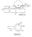
- FIGS. 3A-Care respective cross-sectional, plan, and perspective views of electronic structures according to embodiments of the present invention.
- FIGS. 4A-Eare plan views illustrating conductive interconnects according to embodiments of the present invention.
- a conductive shuntcan be provided to distribute current across a contact surface of a solder structure, such as a solder bump.
- a viacan be provided in an insulating layer exposing portions of a contact pad
- a conductive shuntcan be provided on the exposed portions of the contact pad and on sidewalls of the via
- a solder layercan be provided on the conductive shunt opposite the contact pad and opposite the via sidewalls.
- the conductive shuntcan be a layer of a metal, such as copper, having a thickness of at least 0.5 ⁇ m. Current can thus be conducted through the conductive shunt along sidewalls of the via to provide a more uniform distribution of current density throughout the solder structure. Accordingly, electromigration in the solder structure can be reduced, void formation in the solder structure can be reduced, and/or a useful lifetime of the solder structure can be increased.
- an electronic structuremay include a conductive pad 103 on a substrate 101 , and an insulating layer 107 on the substrate 101 and conductive pad 103 with a via therein so that portions of the conductive pad 103 are free of the insulating layer 107 .
- the electronic structuremay include a conductive trace 105 providing coupling between the conductive pad 103 and other portions of the electronic structure.
- the conductive trace 105may have a first width, and the conductive pad 103 may have a second width greater than the first width.
- the conductive pad 103When viewed perpendicular to the substrate 101 , the conductive pad 103 may have a circular shape, however, other shapes may be provided.
- the via in the insulating layer 107may have a shape similar to that of the conductive pad 103 but smaller so that edge portions of the conductive pad 103 are covered by the insulating layer 107 .
- FIG. 1DA plan view of an example of a conductive pad 103 ′ and a conductive trace 105 ′ according to embodiments of the present invention is illustrated in FIG. 1D .
- a peripheral portion 103 A′ of the conductive pad 103 ′may be covered by an overlying insulating layer, and an interior portion 103 B′ of the conductive pad 103 may be free of an overlying insulating layer. Accordingly, electrical coupling to a solder layer may be provided through the interior portion 103 B′ of the conductive pad 103 ′.
- the conductive pad 103 and conductive trace 105may comprise a layer or layers of conductive materials such as copper, aluminum, nickel, titanium, and/or combinations and/or alloys thereof.
- the conductive pad 103may be electrically coupled to a portion of the substrate opposite the via so that the conductive trace is not required.
- a seed layer 110may be formed on the insulating layer 107 , on sidewalls of the via through the insulating layer, and on portions of the conductive pad 103 free of the insulating layer 107 .
- the seed layer 110may be used as a plating electrode for subsequent electroplating. More particularly, the seed layer 110 may include an adhesion layer 109 to provide adhesion between subsequently electroplated layers and the conductive pad 103 and the insulating layer 107 .
- the adhesion layerfor example, may include a layer of titanium, tungsten, chrome, and/or combinations thereof.
- the seed layer 110may also include a plating conduction layer 111 , such as a layer of copper.
- the plating conduction layermay have a thickness in the range of approximately 0.1 ⁇ m to 0.5 ⁇ m.
- the plating conduction layermay provide electrical conduction for subsequent electroplating.
- the seed layer 110including the adhesion layer 109 and the plating conduction layer 111 , may have a thickness of approximately 0.15 ⁇ m.
- a conductive shunt layer 113 , a barrier layer 115 , and a solder layer 117can then be selectively formed on the seed layer 110 .
- the conductive shunt layer 113 , the barrier layer 115 , and the solder layer 117may be selectively formed on portions of the seed layer 110 opposite the conductive pad 103 , opposite sidewalls of the via exposing the conductive pad 103 , and opposite portions of the insulating layer 107 surrounding the via.
- the conductive shunt layer 113 , the barrier layer 115 , and the solder layer 117may be selectively formed on portions of the seed layer 110 remote from the conductive pad 103 .
- the conductive shunt layer 113 , the barrier layer 115 , and the solder layer 117may be selectively formed by electroplating through a mask. More particularly, a mask may be formed on the seed layer 110 , wherein the mask has a pattern exposing portions of the seed layer 110 on which the conductive shunt layer, the barrier layer, and the solder layer are to be electroplated. The seed layer can then provide an electroplating electrode for successively plating the conductive shunt layer 113 , the barrier layer 115 , and the solder layer 117 . Once the electroplating has been completed, the mask can be removed.
- electroplatinghas been discussed as a means for forming the conductive shunt layer, the barrier layer, and the solder layer
- these layersmay be formed by other means such as electroless plating, evaporation, sputtering, solder paste, solder ball placement, liquid metal jetting, and/or chemical vapor deposition.
- one or more of the conductive shunt layer, the barrier layer, and/or the solder layermay be formed non-selectively across the substrate and then patterned using photolithography to provide the structure illustrated in FIG. 1A .
- the conductive shunt layer 113may be a layer of a metal, such as copper, having a thickness of at least approximately 0.5 ⁇ m. According to particular embodiments, the conductive shunt layer 113 may be a layer of a metal having a thickness of at least approximately 1.0 ⁇ m, and more particularly having a thickness in the range of approximately 1.0 ⁇ m to 5.0 ⁇ m.
- the barrier layer 115may be a layer of a barrier metal, such as nickel, platinum, palladium, and/or combinations thereof, having a thickness in the range of approximately 1 ⁇ m to 2 ⁇ m.
- the solder layer 117may be a layer of lead-tin solder, but other solder materials may be used.
- portions of the seed layer 110may remain free of the conductive shunt layer, the barrier layer, and the solder layer, as shown in FIG. 1A .
- These exposed portions of the seed layer 110may be selectively removed using the solder layer 117 , the barrier layer 115 , and/or the conductive shunt layer 113 as a patterning mask. For example, an etch chemistry may be selected that etches the seed layer selectively with respect to the solder layer 117 and/or the barrier layer 115 . Accordingly, the exposed portions of the seed layer 110 may be selectively removed without requiring a separate masking step, as shown in FIG. 1B , to provide the patterned seed layer 110 ′ which includes the patterned conductive adhesion layer 109 ′ and the patterned plating conduction layer 111 ′.
- the solder layer 117can then be heated above its melting temperature (also referred to as a reflow operation) and then cooled to provide a rounded solder bump 117 ′ as shown in FIG. 1C .
- the solder layer 117may be heated above its melting temperature and then cooled while in contact with a pad of another substrate to provide mechanical and/or electrical coupling between the substrate 101 and the other substrate.
- a relatively thick conductive shunt layer 113current can be distributed more evenly across the solder bump 117 ′. Accordingly, electromigration and/or void formation within the solder bump 117 ′ may be reduced and/or a mean time to failure may be increased.
- the barrier layer 115may help maintain an integrity of the conductive shunt layer 113 during reflow of the solder layer 117 .
- the conductive shunt layer 113may comprise a material that may readily dissolve into solder while the barrier layer 115 may comprise a material that does not readily dissolve into the solder layer 117 during solder reflow. Accordingly, a dissolvable material of the conductive shunt layer 113 may be protected by the barrier layer 115 during solder reflow.
- the conductive shunt layer 113may comprise copper which may readily dissolve into lead-tin solder
- the barrier layer 115may comprise a metal (such as nickel, platinum, palladium, and/or combinations thereof) that may not readily dissolve into lead-tin solder.
- a layer of a passivating material such as goldmay also be provided on the barrier layer 115 .
- conductive shunt layer 113By providing a relatively thick conductive shunt layer 113 extending along exposed portions of the conductive pad 103 , along via sidewalls, and along surface portions of the insulating layer 107 adjacent the via, electrical current flowing between the conductive pad 103 and another substrate may be more evenly distributed across the solder bump 117 ′. Accordingly, electromigration and/or void formation within the solder bump 117 ′ may be reduced, and/or a lifetime of the device may be increased.
- a passivation layersuch as a layer of gold, may be formed on the conductive shunt layer 113 .
- the passivation layercan be formed by plating using the same mask used when forming the conductive shunt layer 113 .
- a solder ballcan then be placed on the passivation layer instead of plating a solder layer.
- the mask and/or the seed layer 110can be removed before or after placement of the solder ball.
- portions of the seed layer 110 covered by the conductive shunt layer 113 and the passivation layercan be maintained while removing portions of the seed layer 110 not covered by the passivation layer and the conductive shunt layer 113 using an etch chemistry that selectively removes materials of the seed layer 110 with respect to the passivation layer and/or the solder ball.
- the conductive shunt layermay be provided as a part of a seed layer, and a separate plating conduction layer may not be required.
- Steps of forming electronic structures including conductive shunt layers as a part of a seed layerare illustrated in FIGS. 2A-C .
- an electronic structuremay include a conductive pad 203 on a substrate 201 , and an insulating layer 207 on the substrate 201 and conductive pad 203 with a via therein so that portions of the conductive pad 203 are free of the insulating layer 207 .
- the electronic structuremay include a conductive trace 205 providing coupling between the conductive pad 203 and other portions of the electronic structure.
- the conductive trace 205may have a first width, and the conductive pad 203 may have a second width greater than the first width.
- the conductive pad 203may have a circular shape, however, other shapes may be provided.
- the via in the insulating layer 207may have a shape similar to that of the conductive pad 203 but smaller so that edge portions of the conductive pad 103 are covered by the insulating layer 207 .
- FIG. 2DA plan view of an example of a conductive pad 203 ′ and a conductive trace 205 ′ according to embodiments of the present invention is illustrated in FIG. 2D .
- a peripheral portion 203 A′ of the conductive pad 203 ′may be covered by an overlying insulating layer, and an interior portion 203 B′ of the conductive pad 203 may be free of an overlying insulating layer. Accordingly, electrical coupling to a solder layer may be provided through the interior portion 203 B′ of the conductive pad 203 ′.
- a seed layer 210may be formed on the insulating layer 207 , on sidewalls of the via through the insulating layer, and on portions of the conductive pad 203 free of the insulating layer 207 .
- the seed layer 210may be used as a plating electrode for subsequent electroplating. More particularly, the seed layer 210 may include a relatively thick conductive shunt layer 213 .
- the seed layer 210may also include an adhesion layer 209 to provide adhesion between the conductive shunt layer 213 and the conductive pad 203 and the insulating layer 207 .
- the adhesion layerfor example, may include a layer of titanium, tungsten, chrome, and/or combinations thereof.
- the conductive shunt layer 213may thus be formed across an entirety of the insulating layer 207 , and the conductive shunt layer 213 may be a layer of a metal such as copper, having a thickness of at least approximately 0.5 ⁇ m. According to particular embodiments, the conductive shunt layer may be a layer of a metal, such as copper, having a thickness of at least approximately 1.0 ⁇ m, and more particularly the conductive shunt layer may have a thickness in the range of approximately 1.0 ⁇ m to 5.0 ⁇ m.
- the conductive shunt layer 213may provide a conduction layer for subsequent electroplating.
- a barrier layer 215 , and a solder layer 217can then be selectively formed on the seed layer 210 .
- the barrier layer 215 , and the solder layer 217may be selectively formed on portions of the seed layer 210 opposite the conductive pad 203 , opposite sidewalls of the via exposing the conductive pad 203 , and opposite portions of the insulating layer 207 surrounding the via.
- the barrier layer 215 , and the solder layer 217may be selectively formed on portions of the seed layer 210 remote from the conductive pad 203 .
- the barrier layer 215 , and the solder layer 217may be selectively formed by electroplating through a mask. More particularly, a mask may be formed on the seed layer 210 , wherein the mask has a pattern exposing portions of the seed layer 210 on which the barrier layer, and the solder layer are to be electroplated. The seed layer can then provide an electroplating electrode for successively plating the barrier layer 215 , and/or the solder layer 217 . Once the electroplating has been completed, the mask can be removed.
- barrier layerWhile electroplating has been discussed as a means for forming the barrier layer, and the solder layer, these layers may be formed by other means such as electroless plating, evaporation, sputtering, solder paste, solder ball placement, liquid metal jetting, and/or chemical vapor deposition. Moreover, one or more of the barrier layer, and/or the solder layer may be formed non-selectively across the substrate and then patterned using photolithography to provide the structure illustrated in FIG. 2A .
- the barrier layer 215may be a layer of a barrier metal (such as nickel, platinum, palladium, and/or combinations thereof) having a thickness in the range of approximately 1 ⁇ m to 2 ⁇ m.
- the solder layer 217may be a layer of lead-tin solder, but other solder materials may be used.
- portions of the seed layer 210may remain free of the barrier layer, and the solder layer, as shown in FIG. 2A .
- These exposed portions of the seed layer 210may be selectively removed using the solder layer 217 and/or the barrier layer 215 as a patterning mask. For example, an etch chemistry may be selected that etches the seed layer selectively with respect to the solder layer 217 and/or the barrier layer 215 . Accordingly, the exposed portions of the seed layer 210 may be selectively removed without requiring a separate masking step as shown in FIG. 2B to provide the patterned seed layer 210 ′ including conductive shunt layer 213 ′.
- the patterned seed layer 210 ′may also include patterned adhesion layer 209 ′.
- the solder layer 217can then be heated above its melting temperature (also referred to as a reflow operation) and then cooled to provide a rounded solder bump 217 ′ as shown in FIG. 2C .
- the solder layer 217may be heated above its melting temperature and then cooled while in contact with a pad of another substrate to provide mechanical and/or electrical coupling between the substrate 201 and the other substrate.
- a relatively thick conductive shunt layer 213current can be distributed more evenly across the solder bump 217 ′. Accordingly, electromigration and/or void formation within the solder bump 217 ′ may be reduced and/or a mean time to failure may be increased.
- the barrier layer 215may help maintain an integrity of the conductive shunt layer 213 during reflow of the solder layer 217 .
- the conductive shunt layer 213may comprise a material that may readily dissolve into solder while the barrier layer 215 may comprise a material that does not readily dissolve into the solder layer 217 during solder reflow. Accordingly, a dissolvable material of the conductive shunt layer 213 may be protected by the barrier layer 215 during solder reflow.
- the conductive shunt layer 213may comprise copper which may readily dissolve into lead-tin solder
- the barrier layer 215may comprise a metal (such as nickel, platinum, palladium, and/or combinations thereof) that may not readily dissolve into lead-tin solder.
- the barrier layer 215may also comprise a layer of a passivating material such as gold.
- electrical current flowing between the conductive pad 203 and another substratemay be more evenly distributed across the solder bump 217 ′. Accordingly, electromigration and/or void formation within the solder bump 217 ′ may be reduced, and/or a lifetime of the device may be increased.
- the conductivity of a conductive shunt layer according to embodiments of the present inventionmay significantly reduce a current density in solder at a critical region of the via.
- an amount of current carried by the conductive shunt layer on the via sidewallscan reduce a current density in the solder by 25% or more.
- electromigration lifetimemay depend on the inverse square of the current density
- a 25% reduction in current densitymay effectively double a lifetime of a device including a conductive shunt layer according to embodiments of the present invention.
- a thickness of a conductive shunt layercan thus be chosen to increase lifetime with respect to electromigration failure.
- Soldersmay be sensitive to electromigration due to their relatively low melting points.
- a critical regionmay be the via where current may be crowded into an area with a radius smaller than that of the body of the bump.
- the higher current densitycan lead to shortened lifetime due to electromigration.
- an electronic structuremay include a conductive pad 303 on substrate 301 , and an insulating layer 307 on the substrate 301 and conductive pad 303 . More particularly, the insulating layer 307 may have a via 308 therein so that portions of the conductive pad 303 are free of the insulating layer 307 .
- a conductive shunt layer 313may be provided on portions of the conductive pad 303 free of the passivation layer 307 , on sidewalls of the via 308 , and on portions of the passivation layer 307 adjacent the via 308 , and a solder layer 317 may be provided on the conductive shunt layer 313 .
- the conductive shunt layer 313may be a layer of a metal, such as copper, having a thickness of at least approximately 0.5 ⁇ m. According to particular embodiments, the conductive shunt layer 313 may be a layer of a metal having a thickness of at least approximately 1.0 ⁇ m, and more particularly in the range of approximately 1.0 ⁇ m to 5.0 ⁇ m.
- the conductive shunt layer 313may include an adhesion layer, such as a layer of titanium, tungsten, chrome, and/or combinations thereof, adjacent the insulating layer 307 and the conductive pad 303 , and the conductive shunt layer 313 may also include a barrier layer, such as a layer of nickel, platinum, palladium, and/or combinations thereof, adjacent the solder layer 317 .
- FIGS. 3B and 3Care top and perspective views, respectively, of portions of the conductive shunt layer 313 and solder layer 317 within the via 308 .
- UBMunderbump metallurgy layer
- the conductivity of a conventional underbump metallurgy layer (UBM)is often ignored in flip chip design because the current flow may be substantially parallel to the thickness direction of the UBM and the UBM may account for only 1% of a total bump thickness.
- currentmay be conducted perpendicular to the thickness direction, through the conductive shunt layer 313 along via 308 sidewalls.
- the conductive shunt layer 313 conductivitycan aid in reducing a current density of the solder layer 317 adjacent the via 308 edge on the conductive pad 303 and in improving a lifetime of a solder joint.
- a current-carrying cross sectional area of a conductive shunt layer 313may be relatively large because it is at the circumference of the cylinder and the conductive shunt layer 313 metal may be more conductive than the solder of solder layer 317 .
- the conductive shunt layer 313 metalmay be more conductive than the solder of solder layer 317 .
- some 31% percent of the currentflows in the conductive shunt layer 313 .
- lifetimeis proportional to inverse square of current density: MTTF ⁇ J ⁇ 2 .
- a 31% percent reduction in solder current densitymay result in an 2.1 fold increase in solder bump lifetime.
- Conductive shunt layersmay thus act as current spreading layers according to embodiments of the present invention.
- a conductive shunt layermay spread current across a bottom surface of a solder layer so that current is more evenly distributed across a cross section of the solder layer parallel with the substrate and so that current crowding in the solder layer at a via corner adjacent a line entry to the conductive pad can be reduced.
- current entering/exiting the solder layercan be spread along via sidewalls and onto a surface of an insulating layer opposite the conductive pad through the conductive shunt layer.
- current crowdingmay be reduced by providing a plurality of current paths to a conductive pad on which a solder layer is formed.
- a conductive pad 401may be provided on an insulating layer of a substrate, and a conductive trace 403 may provide routing of electrical signals between the conductive pad 401 and another portion of the substrate.
- an electrical coupling 405may provide at least two separate current flow paths between the conductive trace 403 and the conductive pad 401 .
- an insulating layermay be provided on the substrate, on the conductive trace 403 , and on the conductive pad 401 .
- a viamay be provided in the insulating layer so that an interior portion 401 A of the conductive pad 401 is free of the passivation layer and so that a peripheral portion 401 B of the conductive pad 401 is covered by the passivation layer.
- the conductive pad 401 , the conductive trace 403 , and the electrical coupling 405may comprise a common structure. More particularly, the conductive pad 401 , the conductive trace 403 , and the electrical coupling 405 may be formed by providing a conductive layer on the substrate, and patterning the conductive layer using photolithography. As shown, the conductive trace 403 may have a first width, and the conductive pad 401 may have a second width greater than the first width. Use of a relatively narrow conductive trace may facilitate routing a plurality of conductive traces/pads on a common substrate, and use of a relatively wide conductive pad may facilitate use of relatively large solder bumps.
- the electrical coupling 405 between the conductive trace 403 and the conductive pad 401may provide at least two separate current flow paths 405 A and 405 B between the conductive trace and the conductive pad. More particularly, the separate current flow paths may be defined by providing a perforation 407 in the electrical coupling 405 between the conductive pad 401 and the conductive trace 403 so that separate current flow paths are provided on either side of the perforation. Moreover, the electrical coupling 405 may be flared to provide contact with a relatively large portion of the conductive pad. While the conductive trace 403 and the electrical coupling 405 are provided with separate reference numbers, it will understood that the electrical coupling may be considered a part of the conductive trace.
- the perforation 407By providing the perforation 407 in a center portion of the electrical coupling, a local current flow through the center of the electrical coupling may be blocked so that a more even distribution of current can be provided to a solder layer on the portion 401 A of the conductive pad 401 free of the passivation layer. Stated in other words, a peak current density in the solder layer at the via edge may be reduced by including the perforation 407 .
- the perforation 407may be circular, but the perforation may have other shapes.
- the perforation 407 ′ in electrical coupling 405 ′may have a slotted shape to provide separate current paths 405 A′ and 405 B′.
- the perforation 407 ′may be flared and/or may have a triangular shape.
- the separate current paths 405 A′ and 405 B′may be viewed as first and second traces extending from the conductive trace 403 to the conductive pad 401 .
- a conductive pad 501may be provided on an insulating layer of a substrate, and a conductive trace 503 may provide routing of electrical signals between the conductive pad 501 and another portion of the substrate.
- an electrical coupling including separate traces 505 A and 505 Bmay provide at least two separate current flow paths between the conductive trace 503 and the conductive pad 501 .
- an insulating layermay be provided on the substrate, on the conductive trace 503 , and on the conductive pad 501 .
- a viamay be provided in the insulating layer so that an interior portion 501 A of the conductive pad 501 is free of the passivation layer and so that a peripheral portion 501 B of the conductive pad 501 is covered by the passivation layer.
- the conductive pad 501 , the conductive trace 503 , and the electrical coupling 505may comprise a common structure. More particularly, the conductive pad 501 , the conductive trace 503 , and the electrical coupling 505 may be formed by providing a conductive layer on the substrate, and patterning the conductive layer using photolithography. As shown, the conductive trace 503 may have a first width, and the conductive pad 501 may have a second width greater than the first width.
- Use of a relatively narrow conductive tracemay facilitate routing a plurality of conductive traces/pads on a common substrate, and use of a relatively wide conductive pad may facilitate use of relatively large solder bumps.
- the electrical coupling 505 between the conductive trace 503 and the conductive pad 501may include at least two separate traces 505 A and 505 B providing at least two separate current flow paths 505 A′ and 505 B′ between the conductive trace and the conductive pad.
- the region 507 ′ between the separate traces 505 A and 505 Bmay be free of a conductive material from which the electrical coupling 505 is formed.
- the separate traces 505 A and 505 Bmay contact opposite sides of the conductive pad 501 as shown in FIG. 4C . Accordingly, current may be provided to the conductive pad 501 and to a solder layer on the interior portion 501 A of the conductive pad 501 from opposite sides thereof.
- a conductive pad 601may be provided on an insulating layer of a substrate, and a conductive trace 603 may provide routing of electrical signals between the conductive pad 601 and another portion of the substrate.
- an electrical coupling including separate traces 605 A and 605 Bmay provide at least two separate current flow paths 605 A′ and 605 B′ between the conductive trace 603 and the conductive pad 601 .
- an insulating layermay be provided on the substrate, on the conductive trace 603 , and on the conductive pad 601 .
- a viamay be provided in the insulating layer so that an interior portion 601 A of the conductive pad 601 is free of the passivation layer and so that a peripheral portion 601 B of the conductive pad 601 is covered by the passivation layer.
- the conductive pad 601 , the conductive trace 603 , and the separate traces 605 A and 605 Bmay comprise a common structure. More particularly, the conductive pad 601 , the conductive trace 603 , and the separate traces 605 A and 605 B may be formed by providing a conductive layer on the substrate, and patterning the conductive layer using photolithography. As shown, the conductive trace 603 may have a first width, and the conductive pad 601 may have a second width greater than the first width.
- Use of a relatively narrow conductive tracemay facilitate routing a plurality of conductive traces/pads on a common substrate, and use of a relatively wide conductive pad may facilitate use of relatively large solder bumps.
- the separate traces 605 A and 605 B between the conductive trace 603 and the conductive pad 601may provide at least two separate current flow paths 605 A′ and 605 B′ between the conductive trace and the conductive pad.
- the region 607 between the separate traces 605 A and 605 Bmay be free of a conductive material from which the electrical coupling 605 , the conductive trace 603 , and the conductive traces 605 A and 605 B are formed.
- the separate traces 605 A and 605 Bmay extend tangentially from the conductive pad 601 , and/or the separate traces 605 A and 605 B may extend in a parallel direction from the contact pad 601 .
- separate current paths 605 A′ and 605 B′may be provided to the conductive pad 601 and to a solder layer on the interior portion 601 A of the conductive pad 601 at relatively widely spaced apart portions of the conductive pad without significantly increasing a width of the conductive pad when combined with the separate traces 605 A and 605 B.
- a conductive pad 701may be provided on an insulating layer of a substrate, and a conductive trace 703 may provide routing of electrical signals between the conductive pad 701 and another portion of the substrate.
- an electrical coupling including separate traces 705 A and 705 Bmay provide at least two separate current flow paths 705 A′ and 705 B′ between the conductive trace 703 and the conductive pad 701 .
- an insulating layermay be provided on the substrate, on the conductive trace 703 , and on the conductive pad 701 .
- a viamay be provided in the insulating layer so that an interior portion 701 A of the conductive pad 701 is free of the passivation layer and so that a peripheral portion 701 B of the conductive pad 701 is covered by the passivation layer.
- the separate traces 705 A and 705 Bmay be symmetric with respect to the conductive trace 703 as discussed above with regard to separate traces 605 A and 605 B of FIG. 4D .
- a third conductive trace 709may be provided between the separate traces 705 A and 705 B. The third conductive trace 709 may provide a more even distribution of current to the conductive pad 701 and to a solder layer on interior portions 701 A of the conductive pad 701 .
- the third trace 709may be centered between the traces 705 A and 705 B so that current paths 705 A′ and 705 B′ provide relatively symmetric current flows, and a width of the third trace 709 may be narrow relative to a width of traces 705 A and 705 B so that a current through path 709 ′ is not too great and so that sufficient current is maintained through paths 705 A′ and 705 B′.
- the conductive pad 701 , the conductive trace 703 , the first and second traces 705 A and 705 B, and the third trace 709may comprise a common structure. More particularly, the conductive pad 701 , the conductive trace 703 , the first and second separate traces 705 A and 705 B, and the third trace 709 may be formed by providing a conductive layer on the substrate, and patterning the conductive layer using photolithography. As shown, the conductive trace 703 may have a first width, and the conductive pad 701 may have a second width greater than the first width. Use of a relatively narrow conductive trace may facilitate routing a plurality of conductive traces/pads on a common substrate, and use of a relatively wide conductive pad may facilitate use of relatively large solder bumps.
- the regions 707 between the separate traces 705 A, 705 B, and 709may be free of a conductive material from which the electrical coupling 705 , the conductive trace 703 , and the conductive traces 705 A, 705 B, and 709 are formed.
- the separate traces 705 A and 705 Bmay extend tangentially from the conductive pad 701 , and/or the separate traces 705 A and 705 B may extend in a parallel direction from the contact pad 701 .
- the separate traces 705 A and 705 Bmay be symmetrical about the trace 709 . Accordingly, separate and spaced apart current paths 705 A′, 705 B′, and 709 may be provided to the conductive pad 701 and to a solder layer on the interior portion 701 A of the conductive pad 701 .
- the conductive pads, conductive traces, and electrical couplings discussed above with regard to FIGS. 4A-Emay be implemented in place of the conductive traces 105 and/or 205 and conductive pads 103 and/or 203 (shown in cross section) of FIGS. 1A-C and 2 A-C.
- peripheral portions 401 B, 501 B, 601 B, and/or 701 B of conductive pads 401 , 510 , 601 , and 701may be covered with an insulating layer, and the insulating layer may have a via therein so that interior portions 401 A, 501 A, 601 A, and/or 701 A of conductive pads 401 , 510 , 601 , and 701 are free of the insulating layer.
- a solder layermay be formed on the interior portions of the conductive pads, on sidewalls of the via in the insulating layer, and on portions of the insulating layer surrounding the via.
- a conductive shunt layermay be provided between the solder layer and the conductive pad and the insulating layer.
- conductive couplings and/or separate traces as discussed above with respect to FIGS. 4A-E and conductive shunt layers as discussed above with respect to FIGS. 1A-C , 2 A-C, and 3 A-Cmay be combined in electronic structures and devices according to embodiments of the present invention.
- Conductive traces 105 and 205 of FIGS. 1A-C and 2 A-Cmay alternately be provided without a flared electrical coupling, without separate current paths, and/or without perforations.
- placement of a trace in contact with a conductive padmay be determined relative to mechanical strain applied to a solder layer on the conductive pad after the solder layer is bonded to a second substrate.
- lateral forcesparallel to the substrates
- the solder layermay strain to absorb the stress. More particularly, one side of the solder layer on the conductive pad may be subjected to tensile strain, and an opposite side of the solder layer on the conductive pad may be subjected to compressive strain.
- a greater current densitymay result in portions of a solder layer on a conductive pad adjacent a conductive trace providing the electrical interconnection for the pad.
- the greater current densitymay result in more rapid electromigration and void formation in portions of the solder layer on a conductive pad adjacent a conductive trace providing electrical interconnection for the pad.
- one or more conductive tracesmay be coupled to the conductive pad adjacent a portion of the solder layer that is subjected to compressive stress. Accordingly, a void formed in the solder layer adjacent the coupling with the conductive trace may be compressed and shunted due to the compressive stress.
- opposite sides of a solder layer on a conductive padmay be subjected to alternating compressive and tensile strains and portions of the solder layer between the opposite sides subjected to the compressive and tensile strains may be neutrally strained.
- a conductive trace or tracesare coupled to the conductive pad adjacent one or more neutrally strained portions of the solder layer.
- a solder layer on the interior portion 501 A of conductive pad 501 of FIG. 4Cmay be subjected to alternating compressive and tensile strains applied parallel to the direction of the trace 503 .
- the separate traces 505 A and 505 Bmay be coupled to opposite sides of the conductive pad that may be neutrally strained.
- Electronic structures according to embodiments of the present inventionmay thus include a primary conductive trace on an electronic substrate wherein the primary conductive trace has a first width, and a conductive pad on the electronic substrate wherein the conductive pad has a second width greater than the first width.
- An electrical coupling between the primary conductive trace and the conductive padmay provide different resistances to current flow across a width thereof. Different resistances may be provided, for example, by providing an opening in the electrical coupling such as the perforation 407 illustrated in FIG. 4A .
- an electrical coupling according to embodiments of the present inventionmay have different thicknesses across a width thereof.
- the electrical coupling 405 of FIG. 4Amay include a relatively thin layer of a conductive material in place of the perforation 407 wherein the relatively thin layer has a thickness that is less that a thickness of the remainder of the electrical coupling.
- the relatively thin layer and the remainder of the electrical couplingmay comprise the same material.
- the electrical couplingmay include a layer of a first conductive material in place of the perforation 407 at a central portion thereof and a layer of a second conductive material along peripheral portions thereof wherein the first and second conductive materials have different resistivities.
- the layer of the second conductive materialmay extend across the electrical coupling on the layer of the first conductive material. Electrical couplings according to embodiments of the present invention may thus provide relatively uniform distribution of current for the conductive pad.
Landscapes
- Engineering & Computer Science (AREA)
- Computer Hardware Design (AREA)
- Microelectronics & Electronic Packaging (AREA)
- Power Engineering (AREA)
- Manufacturing & Machinery (AREA)
- Physics & Mathematics (AREA)
- Condensed Matter Physics & Semiconductors (AREA)
- General Physics & Mathematics (AREA)
- Geometry (AREA)
- Internal Circuitry In Semiconductor Integrated Circuit Devices (AREA)
- Electric Connection Of Electric Components To Printed Circuits (AREA)
- Parts Printed On Printed Circuit Boards (AREA)
Abstract
Description
MTTF∝J−2.
a 31% percent reduction in solder current density may result in an 2.1 fold increase in solder bump lifetime.
Claims (17)
Priority Applications (1)
| Application Number | Priority Date | Filing Date | Title |
|---|---|---|---|
| US12/963,005US8294269B2 (en) | 2002-06-25 | 2010-12-08 | Electronic structures including conductive layers comprising copper and having a thickness of at least 0.5 micrometers |
Applications Claiming Priority (5)
| Application Number | Priority Date | Filing Date | Title |
|---|---|---|---|
| US39151102P | 2002-06-25 | 2002-06-25 | |
| US10/601,938US6960828B2 (en) | 2002-06-25 | 2003-06-23 | Electronic structures including conductive shunt layers |
| US11/226,569US7297631B2 (en) | 2002-06-25 | 2005-09-14 | Methods of forming electronic structures including conductive shunt layers and related structures |
| US11/868,785US7879715B2 (en) | 2002-06-25 | 2007-10-08 | Methods of forming electronic structures including conductive shunt layers and related structures |
| US12/963,005US8294269B2 (en) | 2002-06-25 | 2010-12-08 | Electronic structures including conductive layers comprising copper and having a thickness of at least 0.5 micrometers |
Related Parent Applications (1)
| Application Number | Title | Priority Date | Filing Date |
|---|---|---|---|
| US11/868,785ContinuationUS7879715B2 (en) | 2002-06-25 | 2007-10-08 | Methods of forming electronic structures including conductive shunt layers and related structures |
Publications (2)
| Publication Number | Publication Date |
|---|---|
| US20110084392A1 US20110084392A1 (en) | 2011-04-14 |
| US8294269B2true US8294269B2 (en) | 2012-10-23 |
Family
ID=30000713
Family Applications (4)
| Application Number | Title | Priority Date | Filing Date |
|---|---|---|---|
| US10/601,938Expired - LifetimeUS6960828B2 (en) | 2002-06-25 | 2003-06-23 | Electronic structures including conductive shunt layers |
| US11/226,569Expired - LifetimeUS7297631B2 (en) | 2002-06-25 | 2005-09-14 | Methods of forming electronic structures including conductive shunt layers and related structures |
| US11/868,785Expired - LifetimeUS7879715B2 (en) | 2002-06-25 | 2007-10-08 | Methods of forming electronic structures including conductive shunt layers and related structures |
| US12/963,005Expired - Fee RelatedUS8294269B2 (en) | 2002-06-25 | 2010-12-08 | Electronic structures including conductive layers comprising copper and having a thickness of at least 0.5 micrometers |
Family Applications Before (3)
| Application Number | Title | Priority Date | Filing Date |
|---|---|---|---|
| US10/601,938Expired - LifetimeUS6960828B2 (en) | 2002-06-25 | 2003-06-23 | Electronic structures including conductive shunt layers |
| US11/226,569Expired - LifetimeUS7297631B2 (en) | 2002-06-25 | 2005-09-14 | Methods of forming electronic structures including conductive shunt layers and related structures |
| US11/868,785Expired - LifetimeUS7879715B2 (en) | 2002-06-25 | 2007-10-08 | Methods of forming electronic structures including conductive shunt layers and related structures |
Country Status (4)
| Country | Link |
|---|---|
| US (4) | US6960828B2 (en) |
| AU (1) | AU2003256360A1 (en) |
| TW (1) | TWI306654B (en) |
| WO (1) | WO2004001837A2 (en) |
Cited By (1)
| Publication number | Priority date | Publication date | Assignee | Title |
|---|---|---|---|---|
| US20120146212A1 (en)* | 2010-12-08 | 2012-06-14 | International Business Machines Corporation | Solder bump connections |
Families Citing this family (82)
| Publication number | Priority date | Publication date | Assignee | Title |
|---|---|---|---|---|
| DE60108413T2 (en)* | 2000-11-10 | 2005-06-02 | Unitive Electronics, Inc. | METHOD FOR POSITIONING COMPONENTS WITH THE HELP OF LIQUID DRIVES AND STRUCTURES THEREFOR |
| US6863209B2 (en) | 2000-12-15 | 2005-03-08 | Unitivie International Limited | Low temperature methods of bonding components |
| WO2004001837A2 (en)* | 2002-06-25 | 2003-12-31 | Unitive International Limited | Methods of forming electronic structures including conductive shunt layers and related structures |
| US7531898B2 (en)* | 2002-06-25 | 2009-05-12 | Unitive International Limited | Non-Circular via holes for bumping pads and related structures |
| US7547623B2 (en) | 2002-06-25 | 2009-06-16 | Unitive International Limited | Methods of forming lead free solder bumps |
| TWI225899B (en)* | 2003-02-18 | 2005-01-01 | Unitive Semiconductor Taiwan C | Etching solution and method for manufacturing conductive bump using the etching solution to selectively remove barrier layer |
| US6822327B1 (en)* | 2003-06-13 | 2004-11-23 | Delphi Technologies, Inc. | Flip-chip interconnected with increased current-carrying capability |
| TWI223884B (en)* | 2003-06-30 | 2004-11-11 | Advanced Semiconductor Eng | Under bump metallurgy structure |
| US7115997B2 (en)* | 2003-11-19 | 2006-10-03 | International Business Machines Corporation | Seedless wirebond pad plating |
| TW200603698A (en)* | 2004-04-13 | 2006-01-16 | Unitive International Ltd | Methods of forming solder bumps on exposed metal pads and related structures |
| DE102004031878B3 (en)* | 2004-07-01 | 2005-10-06 | Epcos Ag | Electrical multilayer component with reliable solder contact |
| DE102004047730B4 (en)* | 2004-09-30 | 2017-06-22 | Advanced Micro Devices, Inc. | A method for thinning semiconductor substrates for the production of thin semiconductor wafers |
| US7462317B2 (en) | 2004-11-10 | 2008-12-09 | Enpirion, Inc. | Method of manufacturing an encapsulated package for a magnetic device |
| US7426780B2 (en) | 2004-11-10 | 2008-09-23 | Enpirion, Inc. | Method of manufacturing a power module |
| WO2006053036A2 (en)* | 2004-11-10 | 2006-05-18 | Unitive International Limited | Non-circular via holes for bumping pads and related structures |
| US7332818B2 (en)* | 2005-05-12 | 2008-02-19 | Endicott Interconnect Technologies, Inc. | Multi-chip electronic package with reduced line skew and circuitized substrate for use therein |
| WO2006129135A1 (en)* | 2005-06-02 | 2006-12-07 | Infineon Technologies Ag | An interconnection structure for electronic components, an electronic component and methods for producing the same |
| JP4613708B2 (en)* | 2005-06-23 | 2011-01-19 | ブラザー工業株式会社 | Circuit board and inkjet head |
| US8139362B2 (en) | 2005-10-05 | 2012-03-20 | Enpirion, Inc. | Power module with a magnetic device having a conductive clip |
| US8701272B2 (en) | 2005-10-05 | 2014-04-22 | Enpirion, Inc. | Method of forming a power module with a magnetic device having a conductive clip |
| US7688172B2 (en)* | 2005-10-05 | 2010-03-30 | Enpirion, Inc. | Magnetic device having a conductive clip |
| US8631560B2 (en)* | 2005-10-05 | 2014-01-21 | Enpirion, Inc. | Method of forming a magnetic device having a conductive clip |
| JP4750586B2 (en)* | 2006-02-28 | 2011-08-17 | 住友電工デバイス・イノベーション株式会社 | Semiconductor device, electronic device and manufacturing method thereof |
| US7923836B2 (en)* | 2006-07-21 | 2011-04-12 | International Business Machines Corporation | BLM structure for application to copper pad |
| WO2008054680A2 (en)* | 2006-10-31 | 2008-05-08 | Advanced Micro Devices, Inc. | A metallization layer stack without a terminal aluminum metal layer |
| DE102006051491A1 (en)* | 2006-10-31 | 2008-05-15 | Advanced Micro Devices, Inc., Sunnyvale | Metallization layer stack with an aluminum termination metal layer |
| KR100818525B1 (en) | 2006-12-20 | 2008-03-31 | 동부일렉트로닉스 주식회사 | Image sensor and manufacturing method thereof |
| US7786579B2 (en)* | 2007-05-23 | 2010-08-31 | International Business Machines Corporation | Apparatus for crack prevention in integrated circuit packages |
| US8133529B2 (en)* | 2007-09-10 | 2012-03-13 | Enpirion, Inc. | Method of forming a micromagnetic device |
| US7955868B2 (en)* | 2007-09-10 | 2011-06-07 | Enpirion, Inc. | Method of forming a micromagnetic device |
| US7952459B2 (en)* | 2007-09-10 | 2011-05-31 | Enpirion, Inc. | Micromagnetic device and method of forming the same |
| US7920042B2 (en) | 2007-09-10 | 2011-04-05 | Enpirion, Inc. | Micromagnetic device and method of forming the same |
| US8018315B2 (en)* | 2007-09-10 | 2011-09-13 | Enpirion, Inc. | Power converter employing a micromagnetic device |
| US7911803B2 (en)* | 2007-10-16 | 2011-03-22 | International Business Machines Corporation | Current distribution structure and method |
| KR101374338B1 (en)* | 2007-11-14 | 2014-03-14 | 삼성전자주식회사 | semicondoctor device having through-via and method of forming the same |
| US20090140401A1 (en)* | 2007-11-30 | 2009-06-04 | Stanley Craig Beddingfield | System and Method for Improving Reliability of Integrated Circuit Packages |
| US7868453B2 (en) | 2008-02-15 | 2011-01-11 | International Business Machines Corporation | Solder interconnect pads with current spreading layers |
| US8022543B2 (en)* | 2008-03-25 | 2011-09-20 | International Business Machines Corporation | Underbump metallurgy for enhanced electromigration resistance |
| US8692532B2 (en) | 2008-04-16 | 2014-04-08 | Enpirion, Inc. | Power converter with controller operable in selected modes of operation |
| US8541991B2 (en) | 2008-04-16 | 2013-09-24 | Enpirion, Inc. | Power converter with controller operable in selected modes of operation |
| US9246390B2 (en) | 2008-04-16 | 2016-01-26 | Enpirion, Inc. | Power converter with controller operable in selected modes of operation |
| US8686698B2 (en) | 2008-04-16 | 2014-04-01 | Enpirion, Inc. | Power converter with controller operable in selected modes of operation |
| US8497578B2 (en)* | 2008-05-14 | 2013-07-30 | PAC Tech—Packaging Technologies GmbH | Terminal face contact structure and method of making same |
| US8339802B2 (en)* | 2008-10-02 | 2012-12-25 | Enpirion, Inc. | Module having a stacked magnetic device and semiconductor device and method of forming the same |
| US9054086B2 (en)* | 2008-10-02 | 2015-06-09 | Enpirion, Inc. | Module having a stacked passive element and method of forming the same |
| US8153473B2 (en)* | 2008-10-02 | 2012-04-10 | Empirion, Inc. | Module having a stacked passive element and method of forming the same |
| US8266793B2 (en)* | 2008-10-02 | 2012-09-18 | Enpirion, Inc. | Module having a stacked magnetic device and semiconductor device and method of forming the same |
| US7812462B2 (en)* | 2008-11-04 | 2010-10-12 | National Semiconductor Corporation | Conductive paths for transmitting an electrical signal through an electrical connector |
| US8698463B2 (en) | 2008-12-29 | 2014-04-15 | Enpirion, Inc. | Power converter with a dynamically configurable controller based on a power conversion mode |
| US9548714B2 (en)* | 2008-12-29 | 2017-01-17 | Altera Corporation | Power converter with a dynamically configurable controller and output filter |
| TWI397983B (en)* | 2008-12-31 | 2013-06-01 | Ind Tech Res Inst | Package carrier and bonding structure |
| US7851269B2 (en)* | 2009-02-19 | 2010-12-14 | Intel Corporation | Method of stiffening coreless package substrate |
| US8084858B2 (en) | 2009-04-15 | 2011-12-27 | International Business Machines Corporation | Metal wiring structures for uniform current density in C4 balls |
| US20110210443A1 (en)* | 2010-02-26 | 2011-09-01 | Xilinx, Inc. | Semiconductor device having bucket-shaped under-bump metallization and method of forming same |
| US8405199B2 (en)* | 2010-07-08 | 2013-03-26 | Taiwan Semiconductor Manufacturing Company, Ltd. | Conductive pillar for semiconductor substrate and method of manufacture |
| JP2012038965A (en)* | 2010-08-09 | 2012-02-23 | Lapis Semiconductor Co Ltd | Semiconductor device and manufacturing method of the same |
| US8531030B2 (en)* | 2010-12-16 | 2013-09-10 | Texas Instruments Incorporated | IC device having electromigration resistant feed line structures |
| US8867295B2 (en) | 2010-12-17 | 2014-10-21 | Enpirion, Inc. | Power converter for a memory module |
| US8624392B2 (en) | 2011-06-03 | 2014-01-07 | Taiwan Semiconductor Manufacturing Company, Ltd. | Electrical connection for chip scale packaging |
| US9548281B2 (en)* | 2011-10-07 | 2017-01-17 | Taiwan Semiconductor Manufacturing Company, Ltd. | Electrical connection for chip scale packaging |
| US8912668B2 (en) | 2012-03-01 | 2014-12-16 | Taiwan Semiconductor Manufacturing Company, Ltd. | Electrical connections for chip scale packaging |
| US8741691B2 (en)* | 2012-04-20 | 2014-06-03 | Taiwan Semiconductor Manufacturing Company, Ltd. | Method of fabricating three dimensional integrated circuit |
| US9355978B2 (en) | 2013-03-11 | 2016-05-31 | Taiwan Semiconductor Manufacturing Company, Ltd. | Packaging devices and methods of manufacture thereof |
| US10991669B2 (en) | 2012-07-31 | 2021-04-27 | Mediatek Inc. | Semiconductor package using flip-chip technology |
| TWI562295B (en)* | 2012-07-31 | 2016-12-11 | Mediatek Inc | Semiconductor package and method for fabricating base for semiconductor package |
| US9196573B2 (en) | 2012-07-31 | 2015-11-24 | Taiwan Semiconductor Manufacturing Company, Ltd. | Bump on pad (BOP) bonding structure |
| US9673161B2 (en) | 2012-08-17 | 2017-06-06 | Taiwan Semiconductor Manufacturing Company, Ltd. | Bonded structures for package and substrate |
| US8829673B2 (en) | 2012-08-17 | 2014-09-09 | Taiwan Semiconductor Manufacturing Company, Ltd. | Bonded structures for package and substrate |
| US8952530B2 (en)* | 2012-09-14 | 2015-02-10 | Taiwan Semiconductor Manufacturing Company, Ltd. | Post passivation interconnect structures and methods for forming the same |
| US9269658B2 (en)* | 2013-03-11 | 2016-02-23 | Taiwan Semiconductor Manufacturing Company, Ltd. | Ball amount process in the manufacturing of integrated circuit |
| CN103367315A (en)* | 2013-07-08 | 2013-10-23 | 日月光半导体制造股份有限公司 | Wafer Level Package Construction |
| NO2944700T3 (en) | 2013-07-11 | 2018-03-17 | ||
| US9196529B2 (en)* | 2013-09-27 | 2015-11-24 | Taiwan Semiconductor Manufacturing Company, Ltd. | Contact pad for semiconductor devices |
| WO2015060387A1 (en)* | 2013-10-23 | 2015-04-30 | 京セラ株式会社 | Wiring board and electronic device |
| JP6215755B2 (en) | 2014-04-14 | 2017-10-18 | ルネサスエレクトロニクス株式会社 | Semiconductor device |
| US9509217B2 (en) | 2015-04-20 | 2016-11-29 | Altera Corporation | Asymmetric power flow controller for a power converter and method of operating the same |
| TWI562256B (en)* | 2015-09-07 | 2016-12-11 | Siliconware Precision Industries Co Ltd | Substrate structure |
| US9894767B1 (en)* | 2016-03-20 | 2018-02-13 | Jason Krugman Products, LLC | Concentric circle printed circuit board electrical connection |
| JP6984442B2 (en)* | 2018-01-25 | 2021-12-22 | 富士通株式会社 | Board, electronic device, and board design support method |
| US11024593B2 (en)* | 2018-09-28 | 2021-06-01 | Taiwan Semiconductor Manufacturing Co., Ltd. | Metal bumps and method forming same |
| US12091310B2 (en)* | 2020-05-27 | 2024-09-17 | Apogee Semiconductor, Inc. | Integrated circuit packages having stress-relieving features |
| US12021048B2 (en)* | 2021-08-30 | 2024-06-25 | Taiwan Semiconductor Manufacturing Company, Ltd. | Semiconductor device |
Citations (213)
| Publication number | Priority date | Publication date | Assignee | Title |
|---|---|---|---|---|
| US162257A (en) | 1875-04-20 | Improvement in cider-presses | ||
| US3105869A (en) | 1962-03-23 | 1963-10-01 | Hughes Aircraft Co | Electrical connection of microminiature circuit wafers |
| US3244947A (en) | 1962-06-15 | 1966-04-05 | Slater Electric Inc | Semi-conductor diode and manufacture thereof |
| US3259814A (en) | 1955-05-20 | 1966-07-05 | Rca Corp | Power semiconductor assembly including heat dispersing means |
| US3274458A (en) | 1964-04-02 | 1966-09-20 | Int Rectifier Corp | Extremely high voltage silicon device |
| US3316465A (en) | 1961-03-29 | 1967-04-25 | Siemens Ag | Multi-layer junction semiconductor devices such as controlled rectifiers and transistors, containing electro-positive protective coating |
| US3458925A (en) | 1966-01-20 | 1969-08-05 | Ibm | Method of forming solder mounds on substrates |
| US3461357A (en) | 1967-09-15 | 1969-08-12 | Ibm | Multilevel terminal metallurgy for semiconductor devices |
| US3489965A (en) | 1967-04-04 | 1970-01-13 | Marconi Co Ltd | Insulated gate field effect transistors |
| US3501681A (en) | 1966-07-19 | 1970-03-17 | Union Carbide Corp | Face bonding of semiconductor devices |
| US3586255A (en) | 1967-10-27 | 1971-06-22 | Carpano & Pons | Spinning reel with winding drum brake |
| US3625837A (en) | 1969-09-18 | 1971-12-07 | Singer Co | Electroplating solder-bump connectors on microcircuits |
| US3663184A (en) | 1970-01-23 | 1972-05-16 | Fairchild Camera Instr Co | Solder bump metallization system using a titanium-nickel barrier layer |
| GB1288564A (en) | 1969-01-24 | 1972-09-13 | ||
| US3760238A (en) | 1972-02-28 | 1973-09-18 | Microsystems Int Ltd | Fabrication of beam leads |
| US3770874A (en) | 1970-09-08 | 1973-11-06 | Siemens Ag | Contact members for soldering electrical components |
| US3839727A (en) | 1973-06-25 | 1974-10-01 | Ibm | Semiconductor chip to substrate solder bond using a locally dispersed, ternary intermetallic compound |
| US3871015A (en) | 1969-08-14 | 1975-03-11 | Ibm | Flip chip module with non-uniform connector joints |
| US3871014A (en) | 1969-08-14 | 1975-03-11 | Ibm | Flip chip module with non-uniform solder wettable areas on the substrate |
| US3897871A (en) | 1973-07-26 | 1975-08-05 | Lilly Co Eli | Print album storage case insert |
| US3916080A (en) | 1973-03-24 | 1975-10-28 | Nippon Soken | Electronic circuitry containment device |
| US3942187A (en) | 1969-01-02 | 1976-03-02 | U.S. Philips Corporation | Semiconductor device with multi-layered metal interconnections |
| US3959577A (en) | 1974-06-10 | 1976-05-25 | Westinghouse Electric Corporation | Hermetic seals for insulating-casing structures |
| US3986255A (en) | 1974-11-29 | 1976-10-19 | Itek Corporation | Process for electrically interconnecting chips with substrates employing gold alloy bumps and magnetic materials therein |
| US3993123A (en) | 1975-10-28 | 1976-11-23 | International Business Machines Corporation | Gas encapsulated cooling module |
| US4074342A (en) | 1974-12-20 | 1978-02-14 | International Business Machines Corporation | Electrical package for lsi devices and assembly process therefor |
| US4113587A (en) | 1974-08-05 | 1978-09-12 | Agency Of Industrial Science And Technology | Method for electrochemical machining |
| US4113578A (en) | 1973-05-31 | 1978-09-12 | Honeywell Inc. | Microcircuit device metallization |
| US4168480A (en) | 1978-02-13 | 1979-09-18 | Torr Laboratories, Inc. | Relay assembly |
| US4244002A (en) | 1977-10-19 | 1981-01-06 | Nippon Electric Co., Ltd. | Semiconductor device having bump terminal electrodes |
| US4257905A (en) | 1977-09-06 | 1981-03-24 | The United States Of America As Represented By The United States Department Of Energy | Gaseous insulators for high voltage electrical equipment |
| US4266282A (en) | 1979-03-12 | 1981-05-05 | International Business Machines Corporation | Vertical semiconductor integrated circuit chip packaging |
| US4273859A (en) | 1979-12-31 | 1981-06-16 | Honeywell Information Systems Inc. | Method of forming solder bump terminals on semiconductor elements |
| US4382517A (en) | 1981-02-20 | 1983-05-10 | Metropolitan Wire Corporation | Panels for holding printed circuit boards |
| US4449580A (en) | 1981-06-30 | 1984-05-22 | International Business Machines Corporation | Vertical wall elevated pressure heat dissipation system |
| GB2062963B (en) | 1979-11-12 | 1984-05-23 | Hitachi Ltd | Semiconductor chip mountings |
| US4473263A (en) | 1981-01-21 | 1984-09-25 | Sunstein Drew E | Circuit board mounting device and associated components |
| US4505029A (en) | 1981-03-23 | 1985-03-19 | General Electric Company | Semiconductor device with built-up low resistance contact |
| US4511873A (en) | 1982-07-19 | 1985-04-16 | Bbc Brown, Boveri & Company, Limited | Current transformer insulated by pressurized gas |
| US4532576A (en) | 1983-08-29 | 1985-07-30 | Gte Automatic Electric Incorporated | Printed wiring board file and method of utilizing the same |
| US4545610A (en) | 1983-11-25 | 1985-10-08 | International Business Machines Corporation | Method for forming elongated solder connections between a semiconductor device and a supporting substrate |
| US4563697A (en) | 1982-02-25 | 1986-01-07 | Fuji Electric Company, Ltd. | Semiconductor pressure sensor |
| US4565901A (en) | 1983-06-14 | 1986-01-21 | Mitsubishi Denki Kabushiki Kaisha | Gas-insulated electric device |
| US4657146A (en) | 1985-11-06 | 1987-04-14 | Richard Walters | Adjustable printed circuit board rack for supporting printed circuit boards in a horizontal or a vertical position |
| US4661375A (en) | 1985-04-22 | 1987-04-28 | At&T Technologies, Inc. | Method for increasing the height of solder bumps |
| US4673772A (en) | 1984-10-05 | 1987-06-16 | Hitachi, Ltd. | Electronic circuit device and method of producing the same |
| GB2194387A (en) | 1986-08-20 | 1988-03-02 | Plessey Co Plc | Bonding integrated circuit devices |
| US4733813A (en) | 1985-10-01 | 1988-03-29 | Bull S.A. | Method and apparatus for soldering elements on the corresponding pads of a wafer, in particular a wafer having high-density integrated circuits |
| US4752027A (en) | 1987-02-20 | 1988-06-21 | Hewlett-Packard Company | Method and apparatus for solder bumping of printed circuit boards |
| US4763829A (en) | 1986-06-04 | 1988-08-16 | American Telephone And Telegraph Company, At&T Bell Laboratories | Soldering of electronic components |
| US4783722A (en) | 1985-07-16 | 1988-11-08 | Nippon Telegraph And Telephone Corporation | Interboard connection terminal and method of manufacturing the same |
| US4817850A (en) | 1988-03-28 | 1989-04-04 | Hughes Aircraft Company | Repairable flip-chip bumping |
| US4830264A (en) | 1986-10-08 | 1989-05-16 | International Business Machines Corporation | Method of forming solder terminals for a pinless ceramic module |
| US4840302A (en) | 1988-04-15 | 1989-06-20 | International Business Machines Corporation | Chromium-titanium alloy |
| US4855809A (en) | 1987-11-24 | 1989-08-08 | Texas Instruments Incorporated | Orthogonal chip mount system module and method |
| US4878611A (en) | 1986-05-30 | 1989-11-07 | American Telephone And Telegraph Company, At&T Bell Laboratories | Process for controlling solder joint geometry when surface mounting a leadless integrated circuit package on a substrate |
| US4893403A (en) | 1988-04-15 | 1990-01-16 | Hewlett-Packard Company | Chip alignment method |
| US4897508A (en) | 1988-02-10 | 1990-01-30 | Olin Corporation | Metal electronic package |
| EP0355478A1 (en) | 1988-08-22 | 1990-02-28 | International Business Machines Corporation | Improved lift-off process for terminal metals |
| US4927505A (en) | 1988-07-05 | 1990-05-22 | Motorola Inc. | Metallization scheme providing adhesion and barrier properties |
| US4931410A (en) | 1987-08-25 | 1990-06-05 | Hitachi, Ltd. | Process for producing semiconductor integrated circuit device having copper interconnections and/or wirings, and device produced |
| US4940181A (en) | 1989-04-06 | 1990-07-10 | Motorola, Inc. | Pad grid array for receiving a solder bumped chip carrier |
| US4948754A (en) | 1987-09-02 | 1990-08-14 | Nippondenso Co., Ltd. | Method for making a semiconductor device |
| US4950623A (en) | 1988-08-02 | 1990-08-21 | Microelectronics Center Of North Carolina | Method of building solder bumps |
| US4962058A (en) | 1989-04-14 | 1990-10-09 | International Business Machines Corporation | Process for fabricating multi-level integrated circuit wiring structure from a single metal deposit |
| US4972988A (en) | 1989-07-25 | 1990-11-27 | Mitsubishi Denki Kabushiki Kaisha | Method of soldering semiconductor substrate on supporting plate |
| US5019943A (en) | 1990-02-14 | 1991-05-28 | Unisys Corporation | High density chip stack having a zigzag-shaped face which accommodates connections between chips |
| US5022580A (en) | 1988-03-16 | 1991-06-11 | Plessey Overseas Limited | Vernier structure for flip chip bonded devices |
| US5024372A (en) | 1989-01-03 | 1991-06-18 | Motorola, Inc. | Method of making high density solder bumps and a substrate socket for high density solder bumps |
| US5046161A (en) | 1988-02-23 | 1991-09-03 | Nec Corporation | Flip chip type semiconductor device |
| US5048747A (en) | 1989-06-27 | 1991-09-17 | At&T Bell Laboratories | Solder assembly of components |
| US5113314A (en) | 1991-01-24 | 1992-05-12 | Hewlett-Packard Company | High-speed, high-density chip mounting |
| US5130779A (en) | 1990-06-19 | 1992-07-14 | International Business Machines Corporation | Solder mass having conductive encapsulating arrangement |
| US5130275A (en) | 1990-07-02 | 1992-07-14 | Digital Equipment Corp. | Post fabrication processing of semiconductor chips |
| US5135155A (en) | 1989-08-25 | 1992-08-04 | International Business Machines Corporation | Thermocompression bonding in integrated circuit packaging |
| US5147084A (en) | 1990-07-18 | 1992-09-15 | International Business Machines Corporation | Interconnection structure and test method |
| US5152451A (en) | 1991-04-01 | 1992-10-06 | Motorola, Inc. | Controlled solder oxidation process |
| US5154341A (en) | 1990-12-06 | 1992-10-13 | Motorola Inc. | Noncollapsing multisolder interconnection |
| US5160409A (en) | 1991-08-05 | 1992-11-03 | Motorola, Inc. | Solder plate reflow method for forming a solder bump on a circuit trace intersection |
| US5162257A (en) | 1991-09-13 | 1992-11-10 | Mcnc | Solder bump fabrication method |
| US5171711A (en) | 1990-10-18 | 1992-12-15 | Mitsubishi Denki Kabushiki Kaisha | Method of manufacturing integrated circuit devices |
| DE4205029C1 (en) | 1992-02-19 | 1993-02-11 | Siemens Ag, 8000 Muenchen, De | Micro-mechanical electrostatic relay - has tongue-shaped armature etched from surface of silicon@ substrate |
| US5194137A (en) | 1991-08-05 | 1993-03-16 | Motorola Inc. | Solder plate reflow method for forming solder-bumped terminals |
| US5211807A (en) | 1991-07-02 | 1993-05-18 | Microelectronics Computer & Technology | Titanium-tungsten etching solutions |
| US5216280A (en) | 1989-12-02 | 1993-06-01 | Kabushiki Kaisha Toshiba | Semiconductor integrated circuit device having pads at periphery of semiconductor chip |
| US5227664A (en) | 1988-02-26 | 1993-07-13 | Hitachi, Ltd. | Semiconductor device having particular mounting arrangement |
| US5234149A (en) | 1992-08-28 | 1993-08-10 | At&T Bell Laboratories | Debondable metallic bonding method |
| US5239447A (en) | 1991-09-13 | 1993-08-24 | International Business Machines Corporation | Stepped electronic device package |
| US5240881A (en) | 1991-07-05 | 1993-08-31 | Thomson-Csf | Method of wiring between package outputs and hybrid elements |
| FR2688628A1 (en) | 1992-03-13 | 1993-09-17 | Commissariat Energie Atomique | Three-dimensional assembly of electronic components using microwires and blobs of solder, and method of producing this assembly |
| US5250843A (en) | 1991-03-27 | 1993-10-05 | Integrated System Assemblies Corp. | Multichip integrated circuit modules |
| US5252781A (en) | 1991-05-31 | 1993-10-12 | International Business Machines Corporation | Substrate member having electric lines and apertured insulating film |
| US5251806A (en) | 1990-06-19 | 1993-10-12 | International Business Machines Corporation | Method of forming dual height solder interconnections |
| DE4323799A1 (en) | 1992-07-15 | 1994-01-20 | Toshiba Kawasaki Kk | Semiconductor module coupled to pcb by face-down technology - has contact bumps of solder for connecting chip electrodes to circuit board electrodes, with wall piece not in contact with bumps |
| US5289925A (en) | 1992-03-16 | 1994-03-01 | Martin Newmark | Organizational display for compact disc jewel boxes |
| US5325265A (en) | 1988-11-10 | 1994-06-28 | Mcnc | High performance integrated circuit chip package |
| US5327327A (en) | 1992-10-30 | 1994-07-05 | Texas Instruments Incorporated | Three dimensional assembly of integrated circuit chips |
| US5327013A (en) | 1992-04-30 | 1994-07-05 | Motorola, Inc. | Solder bumping of integrated circuit die |
| US5329068A (en) | 1992-06-10 | 1994-07-12 | Kabushiki Kaisha Toshiba | Semiconductor device |
| EP0609062A1 (en) | 1993-01-27 | 1994-08-03 | Trw Inc. | Mass simultaneous sealing and electrical connection of electronic devices |
| US5335795A (en) | 1991-08-28 | 1994-08-09 | Dwight Chizen | Storage rack for cassettes and compact discs |
| US5347428A (en) | 1992-12-03 | 1994-09-13 | Irvine Sensors Corporation | Module comprising IC memory stack dedicated to and structurally combined with an IC microprocessor chip |
| US5354711A (en) | 1990-06-26 | 1994-10-11 | Commissariat A L'energie Atomique | Process for etching and depositing integrated circuit interconnections and contacts |
| US5381946A (en) | 1992-03-04 | 1995-01-17 | Mcnc | Method of forming differing volume solder bumps |
| US5391514A (en) | 1994-04-19 | 1995-02-21 | International Business Machines Corporation | Low temperature ternary C4 flip chip bonding method |
| US5406701A (en) | 1992-10-02 | 1995-04-18 | Irvine Sensors Corporation | Fabrication of dense parallel solder bump connections |
| US5409862A (en) | 1992-03-24 | 1995-04-25 | Kabushiki Kaisha Toshiba | Method for making aluminum single crystal interconnections on insulators |
| US5424920A (en) | 1992-05-15 | 1995-06-13 | Irvine Sensors Corporation | Non-conductive end layer for integrated stack of IC chips |
| FR2705832B1 (en) | 1993-05-28 | 1995-06-30 | Commissariat Energie Atomique | Method for producing a sealing bead and mechanical strength between a substrate and a chip hybridized by balls on the substrate. |
| US5432729A (en) | 1993-04-23 | 1995-07-11 | Irvine Sensors Corporation | Electronic module comprising a stack of IC chips each interacting with an IC chip secured to the stack |
| US5453582A (en) | 1993-03-11 | 1995-09-26 | The Furukawa Electric Co., Ltd. | Circuit board to be precoated with solder layers and solder circuit board |
| US5462638A (en) | 1994-06-15 | 1995-10-31 | International Business Machines Corporation | Selective etching of TiW for C4 fabrication |
| US5471092A (en) | 1992-09-15 | 1995-11-28 | International Business Machines Corporation | Metallurgical joint including a stress release layer |
| US5470787A (en) | 1994-05-02 | 1995-11-28 | Motorola, Inc. | Semiconductor device solder bump having intrinsic potential for forming an extended eutectic region and method for making and using the same |
| US5475280A (en) | 1992-03-04 | 1995-12-12 | Mcnc | Vertical microelectronic field emission devices |
| US5492235A (en) | 1995-12-18 | 1996-02-20 | Intel Corporation | Process for single mask C4 solder bump fabrication |
| US5539186A (en) | 1992-12-09 | 1996-07-23 | International Business Machines Corporation | Temperature controlled multi-layer module |
| US5542174A (en) | 1994-09-15 | 1996-08-06 | Intel Corporation | Method and apparatus for forming solder balls and solder columns |
| US5547740A (en) | 1995-03-23 | 1996-08-20 | Delco Electronics Corporation | Solderable contacts for flip chip integrated circuit devices |
| US5551627A (en) | 1994-09-29 | 1996-09-03 | Motorola, Inc. | Alloy solder connect assembly and method of connection |
| US5553769A (en) | 1992-11-12 | 1996-09-10 | International Business Machine Corporation | Interconnection of a carrier substrate and a semiconductor device |
| US5557502A (en) | 1995-03-02 | 1996-09-17 | Intel Corporation | Structure of a thermally and electrically enhanced plastic ball grid array package |
| EP0736972A1 (en) | 1995-04-03 | 1996-10-09 | Motorola, Inc. | Plastic encapsulated saw device and method |
| EP0757386A2 (en) | 1995-08-02 | 1997-02-05 | International Business Machines Corporation | Systems interconnected by bumps of joining material |
| US5609287A (en) | 1991-10-04 | 1997-03-11 | Mitsubishi Denki Kabushiki Kaisha | Solder material, junctioning method, junction material, and semiconductor device |
| US5616962A (en) | 1992-01-24 | 1997-04-01 | Kabushiki Kaisha Toshiba | Semiconductor integrated circuit devices having particular terminal geometry |
| US5627396A (en) | 1993-02-01 | 1997-05-06 | Brooktree Corporation | Micromachined relay and method of forming the relay |
| US5634268A (en) | 1995-06-07 | 1997-06-03 | International Business Machines Corporation | Method for making direct chip attach circuit card |
| EP0782191A2 (en) | 1995-12-28 | 1997-07-02 | Lucent Technologies Inc. | Multi-level stacked integrated-circuit-chip assembly |
| US5680296A (en) | 1995-11-07 | 1997-10-21 | Sun Microsystems, Inc. | Card guide with groove having a base portion and ramped portion which restrains an electronic card |
| US5736456A (en) | 1996-03-07 | 1998-04-07 | Micron Technology, Inc. | Method of forming conductive bumps on die for flip chip applications |
| US5739053A (en) | 1992-10-27 | 1998-04-14 | Matsushita Electric Industrial Co., Ltd. | Process for bonding a semiconductor to a circuit substrate including a solder bump transferring step |
| US5744382A (en) | 1992-05-13 | 1998-04-28 | Matsushita Electric Industrial Co., Ltd. | Method of packaging electronic chip component and method of bonding of electrode thereof |
| US5751556A (en) | 1996-03-29 | 1998-05-12 | Intel Corporation | Method and apparatus for reducing warpage of an assembly substrate |
| US5759437A (en) | 1996-10-31 | 1998-06-02 | International Business Machines Corporation | Etching of Ti-W for C4 rework |
| US5796168A (en) | 1996-06-06 | 1998-08-18 | International Business Machines Corporation | Metallic interconnect pad, and integrated circuit structure using same, with reduced undercut |
| US5796591A (en) | 1995-06-07 | 1998-08-18 | International Business Machines Corporation | Direct chip attach circuit card |
| DE19741436A1 (en) | 1997-09-19 | 1998-12-17 | Siemens Ag | Semiconductor device suitable for wire bond and flip-chip mounting |
| US5891756A (en) | 1997-06-27 | 1999-04-06 | Delco Electronics Corporation | Process for converting a wire bond pad to a flip chip solder bump pad and pad formed thereby |
| EP0907207A2 (en) | 1997-08-27 | 1999-04-07 | Nec Corporation | Semiconductor device having alternating long and short contact pads with a fine pitch |
| US5906312A (en) | 1994-12-02 | 1999-05-25 | Franunhofer-Gesellschaft Zur Foerde-Rung Der Angwandten Forschung E.V. | Solder bump for flip chip assembly and method of its fabrication |
| US5963793A (en) | 1996-05-29 | 1999-10-05 | Mcnc | Microelectronic packaging using arched solder columns |
| US5990472A (en) | 1997-09-29 | 1999-11-23 | Mcnc | Microelectronic radiation detectors for detecting and emitting radiation signals |
| US6015505A (en) | 1997-10-30 | 2000-01-18 | International Business Machines Corporation | Process improvements for titanium-tungsten etching in the presence of electroplated C4's |
| US6027957A (en) | 1996-06-27 | 2000-02-22 | University Of Maryland | Controlled solder interdiffusion for high power semiconductor laser diode die bonding |
| US6083773A (en) | 1997-09-16 | 2000-07-04 | Micron Technology, Inc. | Methods of forming flip chip bumps and related flip chip bump constructions |
| US6117299A (en) | 1997-05-09 | 2000-09-12 | Mcnc | Methods of electroplating solder bumps of uniform height on integrated circuit substrates |
| US6121069A (en) | 1997-04-10 | 2000-09-19 | International Business Machines Corporation | Interconnect structure for joining a chip to a circuit card |
| US6134120A (en) | 1998-09-04 | 2000-10-17 | American Standard Inc. | Low profile circuit board mounting arrangement |
| US6133065A (en) | 1997-03-06 | 2000-10-17 | Micron Technology, Inc. | Multi-chip module employing carrier substrate with micromachined alignment structures and method of forming |
| JP2000349111A (en) | 1999-06-03 | 2000-12-15 | Fujitsu Ltd | Electrode for solder joint |
| US6162652A (en) | 1997-12-31 | 2000-12-19 | Intel Corporation | Process for sort testing C4 bumped wafers |
| US6169325B1 (en) | 1997-12-17 | 2001-01-02 | Hitachi, Ltd. | Semiconductor device |
| US6208018B1 (en) | 1997-05-29 | 2001-03-27 | Micron Technology, Inc. | Piggyback multiple dice assembly |
| US6222279B1 (en) | 1995-03-20 | 2001-04-24 | Mcnc | Solder bump fabrication methods and structures including a titanium barrier layer |
| US6221682B1 (en) | 1999-05-28 | 2001-04-24 | Lockheed Martin Corporation | Method and apparatus for evaluating a known good die using both wire bond and flip-chip interconnects |
| US6224690B1 (en) | 1995-12-22 | 2001-05-01 | International Business Machines Corporation | Flip-Chip interconnections using lead-free solders |
| US6232668B1 (en) | 1999-02-02 | 2001-05-15 | Rohm Co. Ltd. | Semiconductor device of chip-on-chip structure and semiconductor chip for use therein |
| US6231743B1 (en) | 2000-01-03 | 2001-05-15 | Motorola, Inc. | Method for forming a semiconductor device |
| US20010011764A1 (en) | 1997-10-20 | 2001-08-09 | Peter Elenius | Chip scale package using large ductile solder balls |
| US6281106B1 (en) | 1999-11-25 | 2001-08-28 | Delphi Technologies, Inc. | Method of solder bumping a circuit component |
| US20010020745A1 (en) | 1998-07-31 | 2001-09-13 | Tongbi Jiang | An interconnect component for a semiconductor die including a ruthenium layer and a method for its fabrication |
| EP1148548A2 (en) | 2000-04-19 | 2001-10-24 | Advanced Interconnect Technology Ltd. | Method of forming lead-free bump interconnections |
| US6320262B1 (en) | 1997-12-05 | 2001-11-20 | Ricoh Company, Ltd. | Semiconductor device and manufacturing method thereof |
| US20010042918A1 (en) | 1998-05-22 | 2001-11-22 | Toshiharu Yanagida | Semiconductor device and method of fabricating the same |
| US6329608B1 (en) | 1995-04-05 | 2001-12-11 | Unitive International Limited | Key-shaped solder bumps and under bump metallurgy |
| US6332988B1 (en) | 1999-06-02 | 2001-12-25 | International Business Machines Corporation | Rework process |
| US6335104B1 (en) | 2000-02-22 | 2002-01-01 | International Business Machines Corporation | Method for preparing a conductive pad for electrical connection and conductive pad formed |
| US20020000665A1 (en) | 1999-04-05 | 2002-01-03 | Alexander L. Barr | Semiconductor device conductive bump and interconnect barrier |
| US6346469B1 (en) | 2000-01-03 | 2002-02-12 | Motorola, Inc. | Semiconductor device and a process for forming the semiconductor device |
| US6388203B1 (en) | 1995-04-04 | 2002-05-14 | Unitive International Limited | Controlled-shaped solder reservoirs for increasing the volume of solder bumps, and structures formed thereby |
| US20020056742A1 (en) | 2000-11-10 | 2002-05-16 | Rinne Glenn A. | Methods and systems for attaching substrates to one another using solder structures having portions with different melting points |
| US20020079576A1 (en) | 2000-06-30 | 2002-06-27 | Krishna Seshan | Ball limiting metallurgy for input/outputs and methods of fabrication |
| US20020086520A1 (en) | 2001-01-02 | 2002-07-04 | Advanced Semiconductor Engineering Inc. | Semiconductor device having bump electrode |
| US6418033B1 (en) | 2000-11-16 | 2002-07-09 | Unitive Electronics, Inc. | Microelectronic packages in which second microelectronic substrates are oriented relative to first microelectronic substrates at acute angles |
| US6415974B2 (en) | 2000-08-01 | 2002-07-09 | Siliconware Precision Industries Co., Ltd. | Structure of solder bumps with improved coplanarity and method of forming solder bumps with improved coplanarity |
| US6419974B1 (en) | 1999-05-27 | 2002-07-16 | General Mills, Inc. | Dairy products and method of preparation |
| JP2002203868A (en) | 2000-12-27 | 2002-07-19 | Toshiba Corp | Electrode formation method |
| US20020096764A1 (en) | 2000-10-13 | 2002-07-25 | Min-Lung Huang | Semiconductor device having bump electrode |
| US6440291B1 (en) | 2000-11-30 | 2002-08-27 | Novellus Systems, Inc. | Controlled induction by use of power supply trigger in electrochemical processing |
| US6476494B1 (en) | 1997-05-27 | 2002-11-05 | Samsung Electronics Co., Ltd. | Silver-tin alloy solder bumps |
| US6475896B1 (en) | 1996-12-04 | 2002-11-05 | Seiko Epson Corporation | Electronic component and semiconductor device, method of making the same and method of mounting the same, circuit board, and electronic instrument |
| US6492197B1 (en) | 2000-05-23 | 2002-12-10 | Unitive Electronics Inc. | Trilayer/bilayer solder bumps and fabrication methods therefor |
| US6495018B1 (en) | 2000-03-13 | 2002-12-17 | Technology Development Associate Operations Limited | Electro-plating apparatus and method |
| US20020197842A1 (en) | 2001-06-21 | 2002-12-26 | Taiwan Semiconductor Manufacturing Co., Ltd. | Bumping process |
| US20030000738A1 (en) | 2001-06-25 | 2003-01-02 | Rumsey Brad D. | Solder resist opening to define a combination pin one indicator and fiducial |
| US20030027379A1 (en) | 2001-08-06 | 2003-02-06 | Hermen Liu | Laser repair operation |
| US20030060040A1 (en) | 1998-07-31 | 2003-03-27 | Industrial Technology Research Institute | Method of electroless plating copper on nitride barrier |
| TW531873B (en) | 2001-06-12 | 2003-05-11 | Advanced Interconnect Tech Ltd | Barrier cap for under bump metal |
| US20030107137A1 (en) | 2001-09-24 | 2003-06-12 | Stierman Roger J. | Micromechanical device contact terminals free of particle generation |
| US20030124833A1 (en) | 2001-12-31 | 2003-07-03 | Ho-Ming Tong | Bump fabrication process |
| US20030134496A1 (en) | 2002-01-12 | 2003-07-17 | Taiwan Semiconductor Manufacturing Co., Ltd. | Method of making a wafer level chip scale package |
| US20030143830A1 (en) | 1999-06-14 | 2003-07-31 | Salman Akram | Method of improving copper interconnect of semiconductor devices for bonding |
| US6617655B1 (en) | 2002-04-05 | 2003-09-09 | Fairchild Semiconductor Corporation | MOSFET device with multiple gate contacts offset from gate contact area and over source area |
| US6622907B2 (en) | 2002-02-19 | 2003-09-23 | International Business Machines Corporation | Sacrificial seed layer process for forming C4 solder bumps |
| US20030186487A1 (en) | 2002-03-28 | 2003-10-02 | Jurgen Hogerl | Method for producing a semiconductor wafer, semiconductor chip, and intermediate semiconductor product |
| US20030218246A1 (en) | 2002-05-22 | 2003-11-27 | Hirofumi Abe | Semiconductor device passing large electric current |
| US6656827B1 (en) | 2002-10-17 | 2003-12-02 | Taiwan Semiconductor Manufacturing Co., Ltd. | Electrical performance enhanced wafer level chip scale package with ground |
| US20040023450A1 (en) | 2001-02-08 | 2004-02-05 | Mitsuaki Katagiri | Semiconductor integrated circuit device and its manufacturing method |
| US20040053483A1 (en) | 2002-06-25 | 2004-03-18 | Nair Krishna K. | Methods of forming electronic structures including conductive shunt layers and related structures |
| US6762122B2 (en) | 2001-09-27 | 2004-07-13 | Unitivie International Limited | Methods of forming metallurgy structures for wire and solder bonding |
| US6793792B2 (en) | 2001-01-12 | 2004-09-21 | Unitive International Limited Curaco | Electroplating methods including maintaining a determined electroplating voltage and related systems |
| US6828510B1 (en) | 1999-06-02 | 2004-12-07 | Ibiden Co., Ltd. | Multilayer printed wiring board and method of manufacturing multilayer printed wiring board |
| US20050012222A1 (en) | 2003-07-15 | 2005-01-20 | Min-Lung Huang | [chip structure] |
| US6853076B2 (en) | 2001-09-21 | 2005-02-08 | Intel Corporation | Copper-containing C4 ball-limiting metallurgy stack for enhanced reliability of packaged structures and method of making same |
| US20060043156A1 (en) | 2004-08-24 | 2006-03-02 | Debelius Christopher A | Dense intermetallic compound layer |
| CN1269607C (en) | 2000-02-25 | 2006-08-16 | 株式会社日立制作所 | Friction mixing welding method |
| US7109112B2 (en) | 2000-08-22 | 2006-09-19 | Micron Technology, Inc. | Method of providing a structure using self-aligned features |
| US20060226544A1 (en) | 2003-08-13 | 2006-10-12 | Shih-Ping Hsu | Semiconductor package substrate having contact pad protective layer formed thereon and method for fabricating the same |
| US20080188071A1 (en)* | 2001-03-05 | 2008-08-07 | Megic Corporation | Low fabrication cost, fine pitch and high reliability solder bump |
| JP4150033B2 (en) | 2005-07-22 | 2008-09-17 | 芝浦メカトロニクス株式会社 | Component mounting equipment |
| US20100117236A1 (en)* | 1998-12-21 | 2010-05-13 | Megica Corporation | Top layers of metal for high performance ic's |
| EP1146552B1 (en) | 2000-04-10 | 2011-10-05 | Agere Systems Guardian Corporation | Interconnections to copper ICs |
Family Cites Families (26)
| Publication number | Priority date | Publication date | Assignee | Title |
|---|---|---|---|---|
| US575156A (en)* | 1897-01-12 | holdsworth | ||
| US557502A (en)* | 1896-03-31 | Car-coupling | ||
| JPS54128669U (en) | 1978-02-27 | 1979-09-07 | ||
| JPS6222978Y2 (en) | 1979-01-31 | 1987-06-11 | ||
| JPS55111127A (en) | 1979-02-19 | 1980-08-27 | Fuji Electric Co Ltd | Method for forming solder bump |
| JPS5773952U (en) | 1980-09-11 | 1982-05-07 | ||
| JPS57197838A (en) | 1981-05-29 | 1982-12-04 | Oki Electric Ind Co Ltd | Semiconductor flip chip element |
| JPS59154041U (en) | 1983-03-31 | 1984-10-16 | 九州積水工業株式会社 | Nori net drying frame |
| JPH0766207B2 (en) | 1986-04-07 | 1995-07-19 | キヤノン株式会社 | Image recorder |
| JPS6399558A (en) | 1986-10-15 | 1988-04-30 | Mitsubishi Electric Corp | semiconductor equipment |
| JPS6399558U (en) | 1986-12-18 | 1988-06-28 | ||
| JPH0793304B2 (en) | 1987-03-11 | 1995-10-09 | 富士通株式会社 | Method of forming bump electrode |
| JPH04150033A (en) | 1990-10-12 | 1992-05-22 | Sharp Corp | Bumps on electronic circuit board and method for forming bumps and circuit patterns on electronic circuit board |
| WO1993002831A1 (en) | 1991-08-05 | 1993-02-18 | Motorola, Inc. | Solder plate reflow method for forming a solder bump on a circuit trace |
| US5923539A (en) | 1992-01-16 | 1999-07-13 | Hitachi, Ltd. | Multilayer circuit substrate with circuit repairing function, and electronic circuit device |
| JPH06116552A (en) | 1992-10-02 | 1994-04-26 | Sekisui Chem Co Ltd | Organic electroluminescent element |
| US5802699A (en) | 1994-06-07 | 1998-09-08 | Tessera, Inc. | Methods of assembling microelectronic assembly with socket for engaging bump leads |
| US5773359A (en) | 1995-12-26 | 1998-06-30 | Motorola, Inc. | Interconnect system and method of fabrication |
| US5851911A (en) | 1996-03-07 | 1998-12-22 | Micron Technology, Inc. | Mask repattern process |
| US6025767A (en) | 1996-08-05 | 2000-02-15 | Mcnc | Encapsulated micro-relay modules and methods of fabricating same |
| US5902686A (en) | 1996-11-21 | 1999-05-11 | Mcnc | Methods for forming an intermetallic region between a solder bump and an under bump metallurgy layer and related structures |
| US5898574A (en) | 1997-09-02 | 1999-04-27 | Tan; Wiling | Self aligning electrical component |
| US6259814B1 (en)* | 1997-10-17 | 2001-07-10 | Canon Kabushiki Kaisha | Image recognition through localized interpretation |
| US5886393A (en) | 1997-11-07 | 1999-03-23 | National Semiconductor Corporation | Bonding wire inductor for use in an integrated circuit package and method |
| US5937320A (en) | 1998-04-08 | 1999-08-10 | International Business Machines Corporation | Barrier layers for electroplated SnPb eutectic solder joints |
| US6338203B1 (en)* | 2000-03-18 | 2002-01-15 | Frederick W. Strickland | Tubing radius alignment tool |
- 2003
- 2003-06-23WOPCT/US2003/020790patent/WO2004001837A2/ennot_activeApplication Discontinuation
- 2003-06-23USUS10/601,938patent/US6960828B2/ennot_activeExpired - Lifetime
- 2003-06-23AUAU2003256360Apatent/AU2003256360A1/ennot_activeAbandoned
- 2003-06-24TWTW092117132Apatent/TWI306654B/ennot_activeIP Right Cessation
- 2005
- 2005-09-14USUS11/226,569patent/US7297631B2/ennot_activeExpired - Lifetime
- 2007
- 2007-10-08USUS11/868,785patent/US7879715B2/ennot_activeExpired - Lifetime
- 2010
- 2010-12-08USUS12/963,005patent/US8294269B2/ennot_activeExpired - Fee Related
Patent Citations (230)
| Publication number | Priority date | Publication date | Assignee | Title |
|---|---|---|---|---|
| US162257A (en) | 1875-04-20 | Improvement in cider-presses | ||
| US3259814A (en) | 1955-05-20 | 1966-07-05 | Rca Corp | Power semiconductor assembly including heat dispersing means |
| US3316465A (en) | 1961-03-29 | 1967-04-25 | Siemens Ag | Multi-layer junction semiconductor devices such as controlled rectifiers and transistors, containing electro-positive protective coating |
| US3105869A (en) | 1962-03-23 | 1963-10-01 | Hughes Aircraft Co | Electrical connection of microminiature circuit wafers |
| US3244947A (en) | 1962-06-15 | 1966-04-05 | Slater Electric Inc | Semi-conductor diode and manufacture thereof |
| US3274458A (en) | 1964-04-02 | 1966-09-20 | Int Rectifier Corp | Extremely high voltage silicon device |
| US3458925A (en) | 1966-01-20 | 1969-08-05 | Ibm | Method of forming solder mounds on substrates |
| US3501681A (en) | 1966-07-19 | 1970-03-17 | Union Carbide Corp | Face bonding of semiconductor devices |
| US3489965A (en) | 1967-04-04 | 1970-01-13 | Marconi Co Ltd | Insulated gate field effect transistors |
| US3461357A (en) | 1967-09-15 | 1969-08-12 | Ibm | Multilevel terminal metallurgy for semiconductor devices |
| US3586255A (en) | 1967-10-27 | 1971-06-22 | Carpano & Pons | Spinning reel with winding drum brake |
| US3942187A (en) | 1969-01-02 | 1976-03-02 | U.S. Philips Corporation | Semiconductor device with multi-layered metal interconnections |
| GB1288564A (en) | 1969-01-24 | 1972-09-13 | ||
| US3871015A (en) | 1969-08-14 | 1975-03-11 | Ibm | Flip chip module with non-uniform connector joints |
| US3871014A (en) | 1969-08-14 | 1975-03-11 | Ibm | Flip chip module with non-uniform solder wettable areas on the substrate |
| US3625837A (en) | 1969-09-18 | 1971-12-07 | Singer Co | Electroplating solder-bump connectors on microcircuits |
| US3663184A (en) | 1970-01-23 | 1972-05-16 | Fairchild Camera Instr Co | Solder bump metallization system using a titanium-nickel barrier layer |
| US3770874A (en) | 1970-09-08 | 1973-11-06 | Siemens Ag | Contact members for soldering electrical components |
| US3760238A (en) | 1972-02-28 | 1973-09-18 | Microsystems Int Ltd | Fabrication of beam leads |
| US3916080A (en) | 1973-03-24 | 1975-10-28 | Nippon Soken | Electronic circuitry containment device |
| US4113578A (en) | 1973-05-31 | 1978-09-12 | Honeywell Inc. | Microcircuit device metallization |
| US3839727A (en) | 1973-06-25 | 1974-10-01 | Ibm | Semiconductor chip to substrate solder bond using a locally dispersed, ternary intermetallic compound |
| US3897871A (en) | 1973-07-26 | 1975-08-05 | Lilly Co Eli | Print album storage case insert |
| US3959577A (en) | 1974-06-10 | 1976-05-25 | Westinghouse Electric Corporation | Hermetic seals for insulating-casing structures |
| US4113587A (en) | 1974-08-05 | 1978-09-12 | Agency Of Industrial Science And Technology | Method for electrochemical machining |
| US3986255A (en) | 1974-11-29 | 1976-10-19 | Itek Corporation | Process for electrically interconnecting chips with substrates employing gold alloy bumps and magnetic materials therein |
| US4074342A (en) | 1974-12-20 | 1978-02-14 | International Business Machines Corporation | Electrical package for lsi devices and assembly process therefor |
| US3993123A (en) | 1975-10-28 | 1976-11-23 | International Business Machines Corporation | Gas encapsulated cooling module |
| US4257905A (en) | 1977-09-06 | 1981-03-24 | The United States Of America As Represented By The United States Department Of Energy | Gaseous insulators for high voltage electrical equipment |
| US4244002A (en) | 1977-10-19 | 1981-01-06 | Nippon Electric Co., Ltd. | Semiconductor device having bump terminal electrodes |
| FR2406893B1 (en) | 1977-10-19 | 1983-10-07 | Nippon Electric Co | |
| US4168480A (en) | 1978-02-13 | 1979-09-18 | Torr Laboratories, Inc. | Relay assembly |
| US4266282A (en) | 1979-03-12 | 1981-05-05 | International Business Machines Corporation | Vertical semiconductor integrated circuit chip packaging |
| GB2062963B (en) | 1979-11-12 | 1984-05-23 | Hitachi Ltd | Semiconductor chip mountings |
| US4273859A (en) | 1979-12-31 | 1981-06-16 | Honeywell Information Systems Inc. | Method of forming solder bump terminals on semiconductor elements |
| US4473263A (en) | 1981-01-21 | 1984-09-25 | Sunstein Drew E | Circuit board mounting device and associated components |
| US4382517A (en) | 1981-02-20 | 1983-05-10 | Metropolitan Wire Corporation | Panels for holding printed circuit boards |
| US4505029A (en) | 1981-03-23 | 1985-03-19 | General Electric Company | Semiconductor device with built-up low resistance contact |
| US4449580A (en) | 1981-06-30 | 1984-05-22 | International Business Machines Corporation | Vertical wall elevated pressure heat dissipation system |
| US4563697A (en) | 1982-02-25 | 1986-01-07 | Fuji Electric Company, Ltd. | Semiconductor pressure sensor |
| US4511873A (en) | 1982-07-19 | 1985-04-16 | Bbc Brown, Boveri & Company, Limited | Current transformer insulated by pressurized gas |
| US4565901A (en) | 1983-06-14 | 1986-01-21 | Mitsubishi Denki Kabushiki Kaisha | Gas-insulated electric device |
| US4532576A (en) | 1983-08-29 | 1985-07-30 | Gte Automatic Electric Incorporated | Printed wiring board file and method of utilizing the same |
| US4545610A (en) | 1983-11-25 | 1985-10-08 | International Business Machines Corporation | Method for forming elongated solder connections between a semiconductor device and a supporting substrate |
| US4673772A (en) | 1984-10-05 | 1987-06-16 | Hitachi, Ltd. | Electronic circuit device and method of producing the same |
| US4661375A (en) | 1985-04-22 | 1987-04-28 | At&T Technologies, Inc. | Method for increasing the height of solder bumps |
| US4897918A (en) | 1985-07-16 | 1990-02-06 | Nippon Telegraph And Telephone | Method of manufacturing an interboard connection terminal |
| US4783722A (en) | 1985-07-16 | 1988-11-08 | Nippon Telegraph And Telephone Corporation | Interboard connection terminal and method of manufacturing the same |
| US4733813A (en) | 1985-10-01 | 1988-03-29 | Bull S.A. | Method and apparatus for soldering elements on the corresponding pads of a wafer, in particular a wafer having high-density integrated circuits |
| US4657146A (en) | 1985-11-06 | 1987-04-14 | Richard Walters | Adjustable printed circuit board rack for supporting printed circuit boards in a horizontal or a vertical position |
| US4878611A (en) | 1986-05-30 | 1989-11-07 | American Telephone And Telegraph Company, At&T Bell Laboratories | Process for controlling solder joint geometry when surface mounting a leadless integrated circuit package on a substrate |
| US4763829A (en) | 1986-06-04 | 1988-08-16 | American Telephone And Telegraph Company, At&T Bell Laboratories | Soldering of electronic components |
| GB2194387A (en) | 1986-08-20 | 1988-03-02 | Plessey Co Plc | Bonding integrated circuit devices |
| US4830264A (en) | 1986-10-08 | 1989-05-16 | International Business Machines Corporation | Method of forming solder terminals for a pinless ceramic module |
| US4752027A (en) | 1987-02-20 | 1988-06-21 | Hewlett-Packard Company | Method and apparatus for solder bumping of printed circuit boards |
| US4931410A (en) | 1987-08-25 | 1990-06-05 | Hitachi, Ltd. | Process for producing semiconductor integrated circuit device having copper interconnections and/or wirings, and device produced |
| US4948754A (en) | 1987-09-02 | 1990-08-14 | Nippondenso Co., Ltd. | Method for making a semiconductor device |
| US4855809A (en) | 1987-11-24 | 1989-08-08 | Texas Instruments Incorporated | Orthogonal chip mount system module and method |
| US4897508A (en) | 1988-02-10 | 1990-01-30 | Olin Corporation | Metal electronic package |
| US5046161A (en) | 1988-02-23 | 1991-09-03 | Nec Corporation | Flip chip type semiconductor device |
| US5227664A (en) | 1988-02-26 | 1993-07-13 | Hitachi, Ltd. | Semiconductor device having particular mounting arrangement |
| US5022580A (en) | 1988-03-16 | 1991-06-11 | Plessey Overseas Limited | Vernier structure for flip chip bonded devices |
| US4817850A (en) | 1988-03-28 | 1989-04-04 | Hughes Aircraft Company | Repairable flip-chip bumping |
| US4840302A (en) | 1988-04-15 | 1989-06-20 | International Business Machines Corporation | Chromium-titanium alloy |
| US4893403A (en) | 1988-04-15 | 1990-01-16 | Hewlett-Packard Company | Chip alignment method |
| US4927505A (en) | 1988-07-05 | 1990-05-22 | Motorola Inc. | Metallization scheme providing adhesion and barrier properties |
| US4950623A (en) | 1988-08-02 | 1990-08-21 | Microelectronics Center Of North Carolina | Method of building solder bumps |
| EP0355478A1 (en) | 1988-08-22 | 1990-02-28 | International Business Machines Corporation | Improved lift-off process for terminal metals |
| US5325265A (en) | 1988-11-10 | 1994-06-28 | Mcnc | High performance integrated circuit chip package |
| US5024372A (en) | 1989-01-03 | 1991-06-18 | Motorola, Inc. | Method of making high density solder bumps and a substrate socket for high density solder bumps |
| US4940181A (en) | 1989-04-06 | 1990-07-10 | Motorola, Inc. | Pad grid array for receiving a solder bumped chip carrier |
| US4962058A (en) | 1989-04-14 | 1990-10-09 | International Business Machines Corporation | Process for fabricating multi-level integrated circuit wiring structure from a single metal deposit |
| US5048747A (en) | 1989-06-27 | 1991-09-17 | At&T Bell Laboratories | Solder assembly of components |
| US4972988A (en) | 1989-07-25 | 1990-11-27 | Mitsubishi Denki Kabushiki Kaisha | Method of soldering semiconductor substrate on supporting plate |
| US5135155A (en) | 1989-08-25 | 1992-08-04 | International Business Machines Corporation | Thermocompression bonding in integrated circuit packaging |
| US5216280A (en) | 1989-12-02 | 1993-06-01 | Kabushiki Kaisha Toshiba | Semiconductor integrated circuit device having pads at periphery of semiconductor chip |
| US5019943A (en) | 1990-02-14 | 1991-05-28 | Unisys Corporation | High density chip stack having a zigzag-shaped face which accommodates connections between chips |
| US5130779A (en) | 1990-06-19 | 1992-07-14 | International Business Machines Corporation | Solder mass having conductive encapsulating arrangement |
| US5251806A (en) | 1990-06-19 | 1993-10-12 | International Business Machines Corporation | Method of forming dual height solder interconnections |
| US5354711A (en) | 1990-06-26 | 1994-10-11 | Commissariat A L'energie Atomique | Process for etching and depositing integrated circuit interconnections and contacts |
| US5130275A (en) | 1990-07-02 | 1992-07-14 | Digital Equipment Corp. | Post fabrication processing of semiconductor chips |
| US5147084A (en) | 1990-07-18 | 1992-09-15 | International Business Machines Corporation | Interconnection structure and test method |
| US5171711A (en) | 1990-10-18 | 1992-12-15 | Mitsubishi Denki Kabushiki Kaisha | Method of manufacturing integrated circuit devices |
| US5154341A (en) | 1990-12-06 | 1992-10-13 | Motorola Inc. | Noncollapsing multisolder interconnection |
| US5113314A (en) | 1991-01-24 | 1992-05-12 | Hewlett-Packard Company | High-speed, high-density chip mounting |
| US5250843A (en) | 1991-03-27 | 1993-10-05 | Integrated System Assemblies Corp. | Multichip integrated circuit modules |
| US5152451A (en) | 1991-04-01 | 1992-10-06 | Motorola, Inc. | Controlled solder oxidation process |
| US5252781A (en) | 1991-05-31 | 1993-10-12 | International Business Machines Corporation | Substrate member having electric lines and apertured insulating film |
| US5211807A (en) | 1991-07-02 | 1993-05-18 | Microelectronics Computer & Technology | Titanium-tungsten etching solutions |
| US5240881A (en) | 1991-07-05 | 1993-08-31 | Thomson-Csf | Method of wiring between package outputs and hybrid elements |
| US5160409A (en) | 1991-08-05 | 1992-11-03 | Motorola, Inc. | Solder plate reflow method for forming a solder bump on a circuit trace intersection |
| US5194137A (en) | 1991-08-05 | 1993-03-16 | Motorola Inc. | Solder plate reflow method for forming solder-bumped terminals |
| US5335795A (en) | 1991-08-28 | 1994-08-09 | Dwight Chizen | Storage rack for cassettes and compact discs |
| US5239447A (en) | 1991-09-13 | 1993-08-24 | International Business Machines Corporation | Stepped electronic device package |
| EP0603296B1 (en) | 1991-09-13 | 1997-08-13 | Mcnc | Solder bump fabrication method and solder bumps formed thereby |
| US5162257A (en) | 1991-09-13 | 1992-11-10 | Mcnc | Solder bump fabrication method |
| US5293006A (en) | 1991-09-13 | 1994-03-08 | Mcnc | Solder bump including circular lip |
| US5609287A (en) | 1991-10-04 | 1997-03-11 | Mitsubishi Denki Kabushiki Kaisha | Solder material, junctioning method, junction material, and semiconductor device |
| US5616962A (en) | 1992-01-24 | 1997-04-01 | Kabushiki Kaisha Toshiba | Semiconductor integrated circuit devices having particular terminal geometry |
| DE4205029C1 (en) | 1992-02-19 | 1993-02-11 | Siemens Ag, 8000 Muenchen, De | Micro-mechanical electrostatic relay - has tongue-shaped armature etched from surface of silicon@ substrate |
| US5475280A (en) | 1992-03-04 | 1995-12-12 | Mcnc | Vertical microelectronic field emission devices |
| US5381946A (en) | 1992-03-04 | 1995-01-17 | Mcnc | Method of forming differing volume solder bumps |
| FR2688628A1 (en) | 1992-03-13 | 1993-09-17 | Commissariat Energie Atomique | Three-dimensional assembly of electronic components using microwires and blobs of solder, and method of producing this assembly |
| US5289925A (en) | 1992-03-16 | 1994-03-01 | Martin Newmark | Organizational display for compact disc jewel boxes |
| US5409862A (en) | 1992-03-24 | 1995-04-25 | Kabushiki Kaisha Toshiba | Method for making aluminum single crystal interconnections on insulators |
| US5327013A (en) | 1992-04-30 | 1994-07-05 | Motorola, Inc. | Solder bumping of integrated circuit die |
| US5744382A (en) | 1992-05-13 | 1998-04-28 | Matsushita Electric Industrial Co., Ltd. | Method of packaging electronic chip component and method of bonding of electrode thereof |
| US5424920A (en) | 1992-05-15 | 1995-06-13 | Irvine Sensors Corporation | Non-conductive end layer for integrated stack of IC chips |
| US5329068A (en) | 1992-06-10 | 1994-07-12 | Kabushiki Kaisha Toshiba | Semiconductor device |
| DE4323799A1 (en) | 1992-07-15 | 1994-01-20 | Toshiba Kawasaki Kk | Semiconductor module coupled to pcb by face-down technology - has contact bumps of solder for connecting chip electrodes to circuit board electrodes, with wall piece not in contact with bumps |
| US5234149A (en) | 1992-08-28 | 1993-08-10 | At&T Bell Laboratories | Debondable metallic bonding method |
| US5471092A (en) | 1992-09-15 | 1995-11-28 | International Business Machines Corporation | Metallurgical joint including a stress release layer |
| US5406701A (en) | 1992-10-02 | 1995-04-18 | Irvine Sensors Corporation | Fabrication of dense parallel solder bump connections |
| US5739053A (en) | 1992-10-27 | 1998-04-14 | Matsushita Electric Industrial Co., Ltd. | Process for bonding a semiconductor to a circuit substrate including a solder bump transferring step |
| US5327327A (en) | 1992-10-30 | 1994-07-05 | Texas Instruments Incorporated | Three dimensional assembly of integrated circuit chips |
| US5859470A (en) | 1992-11-12 | 1999-01-12 | International Business Machines Corporation | Interconnection of a carrier substrate and a semiconductor device |
| US5553769A (en) | 1992-11-12 | 1996-09-10 | International Business Machine Corporation | Interconnection of a carrier substrate and a semiconductor device |
| US5920125A (en) | 1992-11-12 | 1999-07-06 | International Business Machines Corporation | Interconnection of a carrier substrate and a semiconductor device |
| US5347428A (en) | 1992-12-03 | 1994-09-13 | Irvine Sensors Corporation | Module comprising IC memory stack dedicated to and structurally combined with an IC microprocessor chip |
| US5539186A (en) | 1992-12-09 | 1996-07-23 | International Business Machines Corporation | Temperature controlled multi-layer module |
| EP0609062A1 (en) | 1993-01-27 | 1994-08-03 | Trw Inc. | Mass simultaneous sealing and electrical connection of electronic devices |
| US5627396A (en) | 1993-02-01 | 1997-05-06 | Brooktree Corporation | Micromachined relay and method of forming the relay |
| US5453582A (en) | 1993-03-11 | 1995-09-26 | The Furukawa Electric Co., Ltd. | Circuit board to be precoated with solder layers and solder circuit board |
| US5432729A (en) | 1993-04-23 | 1995-07-11 | Irvine Sensors Corporation | Electronic module comprising a stack of IC chips each interacting with an IC chip secured to the stack |
| FR2705832B1 (en) | 1993-05-28 | 1995-06-30 | Commissariat Energie Atomique | Method for producing a sealing bead and mechanical strength between a substrate and a chip hybridized by balls on the substrate. |
| US6238951B1 (en) | 1993-05-28 | 2001-05-29 | Commissariat A L'energie Atomique | Process for producing a sealing and mechanical strength ring between a substrate and a chip hybridized by bumps on the substrate |
| US5391514A (en) | 1994-04-19 | 1995-02-21 | International Business Machines Corporation | Low temperature ternary C4 flip chip bonding method |
| US5470787A (en) | 1994-05-02 | 1995-11-28 | Motorola, Inc. | Semiconductor device solder bump having intrinsic potential for forming an extended eutectic region and method for making and using the same |
| US5462638A (en) | 1994-06-15 | 1995-10-31 | International Business Machines Corporation | Selective etching of TiW for C4 fabrication |
| US5542174A (en) | 1994-09-15 | 1996-08-06 | Intel Corporation | Method and apparatus for forming solder balls and solder columns |
| US5551627A (en) | 1994-09-29 | 1996-09-03 | Motorola, Inc. | Alloy solder connect assembly and method of connection |
| US5906312A (en) | 1994-12-02 | 1999-05-25 | Franunhofer-Gesellschaft Zur Foerde-Rung Der Angwandten Forschung E.V. | Solder bump for flip chip assembly and method of its fabrication |
| US5557502A (en) | 1995-03-02 | 1996-09-17 | Intel Corporation | Structure of a thermally and electrically enhanced plastic ball grid array package |
| US6222279B1 (en) | 1995-03-20 | 2001-04-24 | Mcnc | Solder bump fabrication methods and structures including a titanium barrier layer |
| US5547740A (en) | 1995-03-23 | 1996-08-20 | Delco Electronics Corporation | Solderable contacts for flip chip integrated circuit devices |
| EP0736972A1 (en) | 1995-04-03 | 1996-10-09 | Motorola, Inc. | Plastic encapsulated saw device and method |
| US6388203B1 (en) | 1995-04-04 | 2002-05-14 | Unitive International Limited | Controlled-shaped solder reservoirs for increasing the volume of solder bumps, and structures formed thereby |
| US6392163B1 (en) | 1995-04-04 | 2002-05-21 | Unitive International Limited | Controlled-shaped solder reservoirs for increasing the volume of solder bumps |
| US6329608B1 (en) | 1995-04-05 | 2001-12-11 | Unitive International Limited | Key-shaped solder bumps and under bump metallurgy |
| US6389691B1 (en) | 1995-04-05 | 2002-05-21 | Unitive International Limited | Methods for forming integrated redistribution routing conductors and solder bumps |
| US5796591A (en) | 1995-06-07 | 1998-08-18 | International Business Machines Corporation | Direct chip attach circuit card |
| US5634268A (en) | 1995-06-07 | 1997-06-03 | International Business Machines Corporation | Method for making direct chip attach circuit card |
| EP0757386A2 (en) | 1995-08-02 | 1997-02-05 | International Business Machines Corporation | Systems interconnected by bumps of joining material |
| US5680296A (en) | 1995-11-07 | 1997-10-21 | Sun Microsystems, Inc. | Card guide with groove having a base portion and ramped portion which restrains an electronic card |
| US5492235A (en) | 1995-12-18 | 1996-02-20 | Intel Corporation | Process for single mask C4 solder bump fabrication |
| US6224690B1 (en) | 1995-12-22 | 2001-05-01 | International Business Machines Corporation | Flip-Chip interconnections using lead-free solders |
| EP0782191A2 (en) | 1995-12-28 | 1997-07-02 | Lucent Technologies Inc. | Multi-level stacked integrated-circuit-chip assembly |
| US5736456A (en) | 1996-03-07 | 1998-04-07 | Micron Technology, Inc. | Method of forming conductive bumps on die for flip chip applications |
| US5751556A (en) | 1996-03-29 | 1998-05-12 | Intel Corporation | Method and apparatus for reducing warpage of an assembly substrate |
| US5963793A (en) | 1996-05-29 | 1999-10-05 | Mcnc | Microelectronic packaging using arched solder columns |
| US5796168A (en) | 1996-06-06 | 1998-08-18 | International Business Machines Corporation | Metallic interconnect pad, and integrated circuit structure using same, with reduced undercut |
| US6027957A (en) | 1996-06-27 | 2000-02-22 | University Of Maryland | Controlled solder interdiffusion for high power semiconductor laser diode die bonding |
| US5759437A (en) | 1996-10-31 | 1998-06-02 | International Business Machines Corporation | Etching of Ti-W for C4 rework |
| US6475896B1 (en) | 1996-12-04 | 2002-11-05 | Seiko Epson Corporation | Electronic component and semiconductor device, method of making the same and method of mounting the same, circuit board, and electronic instrument |
| US6133065A (en) | 1997-03-06 | 2000-10-17 | Micron Technology, Inc. | Multi-chip module employing carrier substrate with micromachined alignment structures and method of forming |
| US6121069A (en) | 1997-04-10 | 2000-09-19 | International Business Machines Corporation | Interconnect structure for joining a chip to a circuit card |
| US6117299A (en) | 1997-05-09 | 2000-09-12 | Mcnc | Methods of electroplating solder bumps of uniform height on integrated circuit substrates |
| US6476494B1 (en) | 1997-05-27 | 2002-11-05 | Samsung Electronics Co., Ltd. | Silver-tin alloy solder bumps |
| US6208018B1 (en) | 1997-05-29 | 2001-03-27 | Micron Technology, Inc. | Piggyback multiple dice assembly |
| US5891756A (en) | 1997-06-27 | 1999-04-06 | Delco Electronics Corporation | Process for converting a wire bond pad to a flip chip solder bump pad and pad formed thereby |
| EP0907207A2 (en) | 1997-08-27 | 1999-04-07 | Nec Corporation | Semiconductor device having alternating long and short contact pads with a fine pitch |
| US6083773A (en) | 1997-09-16 | 2000-07-04 | Micron Technology, Inc. | Methods of forming flip chip bumps and related flip chip bump constructions |
| DE19741436A1 (en) | 1997-09-19 | 1998-12-17 | Siemens Ag | Semiconductor device suitable for wire bond and flip-chip mounting |
| US5990472A (en) | 1997-09-29 | 1999-11-23 | Mcnc | Microelectronic radiation detectors for detecting and emitting radiation signals |
| US6441487B2 (en) | 1997-10-20 | 2002-08-27 | Flip Chip Technologies, L.L.C. | Chip scale package using large ductile solder balls |
| US20010011764A1 (en) | 1997-10-20 | 2001-08-09 | Peter Elenius | Chip scale package using large ductile solder balls |
| US6015505A (en) | 1997-10-30 | 2000-01-18 | International Business Machines Corporation | Process improvements for titanium-tungsten etching in the presence of electroplated C4's |
| US6320262B1 (en) | 1997-12-05 | 2001-11-20 | Ricoh Company, Ltd. | Semiconductor device and manufacturing method thereof |
| US6169325B1 (en) | 1997-12-17 | 2001-01-02 | Hitachi, Ltd. | Semiconductor device |
| US6162652A (en) | 1997-12-31 | 2000-12-19 | Intel Corporation | Process for sort testing C4 bumped wafers |
| US20010042918A1 (en) | 1998-05-22 | 2001-11-22 | Toshiharu Yanagida | Semiconductor device and method of fabricating the same |
| US6452271B2 (en) | 1998-07-31 | 2002-09-17 | Micron Technology, Inc. | Interconnect component for a semiconductor die including a ruthenium layer and a method for its fabrication |
| US20010020745A1 (en) | 1998-07-31 | 2001-09-13 | Tongbi Jiang | An interconnect component for a semiconductor die including a ruthenium layer and a method for its fabrication |
| US20030060040A1 (en) | 1998-07-31 | 2003-03-27 | Industrial Technology Research Institute | Method of electroless plating copper on nitride barrier |
| US6134120A (en) | 1998-09-04 | 2000-10-17 | American Standard Inc. | Low profile circuit board mounting arrangement |
| US20100117236A1 (en)* | 1998-12-21 | 2010-05-13 | Megica Corporation | Top layers of metal for high performance ic's |
| US6232668B1 (en) | 1999-02-02 | 2001-05-15 | Rohm Co. Ltd. | Semiconductor device of chip-on-chip structure and semiconductor chip for use therein |
| US20020000665A1 (en) | 1999-04-05 | 2002-01-03 | Alexander L. Barr | Semiconductor device conductive bump and interconnect barrier |
| US20020093098A1 (en) | 1999-04-05 | 2002-07-18 | Barr Alexander L. | Semiconductor device and method of formation |
| US6419974B1 (en) | 1999-05-27 | 2002-07-16 | General Mills, Inc. | Dairy products and method of preparation |
| US6221682B1 (en) | 1999-05-28 | 2001-04-24 | Lockheed Martin Corporation | Method and apparatus for evaluating a known good die using both wire bond and flip-chip interconnects |
| US6828510B1 (en) | 1999-06-02 | 2004-12-07 | Ibiden Co., Ltd. | Multilayer printed wiring board and method of manufacturing multilayer printed wiring board |
| US6332988B1 (en) | 1999-06-02 | 2001-12-25 | International Business Machines Corporation | Rework process |
| JP2000349111A (en) | 1999-06-03 | 2000-12-15 | Fujitsu Ltd | Electrode for solder joint |
| US20030143830A1 (en) | 1999-06-14 | 2003-07-31 | Salman Akram | Method of improving copper interconnect of semiconductor devices for bonding |
| US6835643B2 (en) | 1999-06-14 | 2004-12-28 | Micron Technology, Inc. | Method of improving copper interconnects of semiconductor devices for bonding |
| US6281106B1 (en) | 1999-11-25 | 2001-08-28 | Delphi Technologies, Inc. | Method of solder bumping a circuit component |
| US6346469B1 (en) | 2000-01-03 | 2002-02-12 | Motorola, Inc. | Semiconductor device and a process for forming the semiconductor device |
| US6231743B1 (en) | 2000-01-03 | 2001-05-15 | Motorola, Inc. | Method for forming a semiconductor device |
| US6335104B1 (en) | 2000-02-22 | 2002-01-01 | International Business Machines Corporation | Method for preparing a conductive pad for electrical connection and conductive pad formed |
| CN1269607C (en) | 2000-02-25 | 2006-08-16 | 株式会社日立制作所 | Friction mixing welding method |
| US6495018B1 (en) | 2000-03-13 | 2002-12-17 | Technology Development Associate Operations Limited | Electro-plating apparatus and method |
| EP1146552B1 (en) | 2000-04-10 | 2011-10-05 | Agere Systems Guardian Corporation | Interconnections to copper ICs |
| EP1148548A2 (en) | 2000-04-19 | 2001-10-24 | Advanced Interconnect Technology Ltd. | Method of forming lead-free bump interconnections |
| US6492197B1 (en) | 2000-05-23 | 2002-12-10 | Unitive Electronics Inc. | Trilayer/bilayer solder bumps and fabrication methods therefor |
| US20020079576A1 (en) | 2000-06-30 | 2002-06-27 | Krishna Seshan | Ball limiting metallurgy for input/outputs and methods of fabrication |
| US6521996B1 (en) | 2000-06-30 | 2003-02-18 | Intel Corporation | Ball limiting metallurgy for input/outputs and methods of fabrication |
| US6415974B2 (en) | 2000-08-01 | 2002-07-09 | Siliconware Precision Industries Co., Ltd. | Structure of solder bumps with improved coplanarity and method of forming solder bumps with improved coplanarity |
| US7109112B2 (en) | 2000-08-22 | 2006-09-19 | Micron Technology, Inc. | Method of providing a structure using self-aligned features |
| US6452270B1 (en) | 2000-10-13 | 2002-09-17 | Advanced Semiconductor Engineering, Inc. | Semiconductor device having bump electrode |
| US20020096764A1 (en) | 2000-10-13 | 2002-07-25 | Min-Lung Huang | Semiconductor device having bump electrode |
| US20020056742A1 (en) | 2000-11-10 | 2002-05-16 | Rinne Glenn A. | Methods and systems for attaching substrates to one another using solder structures having portions with different melting points |
| US6418033B1 (en) | 2000-11-16 | 2002-07-09 | Unitive Electronics, Inc. | Microelectronic packages in which second microelectronic substrates are oriented relative to first microelectronic substrates at acute angles |
| US6440291B1 (en) | 2000-11-30 | 2002-08-27 | Novellus Systems, Inc. | Controlled induction by use of power supply trigger in electrochemical processing |
| JP2002203868A (en) | 2000-12-27 | 2002-07-19 | Toshiba Corp | Electrode formation method |
| US20020086520A1 (en) | 2001-01-02 | 2002-07-04 | Advanced Semiconductor Engineering Inc. | Semiconductor device having bump electrode |
| US6793792B2 (en) | 2001-01-12 | 2004-09-21 | Unitive International Limited Curaco | Electroplating methods including maintaining a determined electroplating voltage and related systems |
| US20040023450A1 (en) | 2001-02-08 | 2004-02-05 | Mitsuaki Katagiri | Semiconductor integrated circuit device and its manufacturing method |
| US20080188071A1 (en)* | 2001-03-05 | 2008-08-07 | Megic Corporation | Low fabrication cost, fine pitch and high reliability solder bump |
| TW531873B (en) | 2001-06-12 | 2003-05-11 | Advanced Interconnect Tech Ltd | Barrier cap for under bump metal |
| US6620722B2 (en) | 2001-06-21 | 2003-09-16 | Taiwan Semiconductor Manufacturing Co., Ltd | Bumping process |
| US20020197842A1 (en) | 2001-06-21 | 2002-12-26 | Taiwan Semiconductor Manufacturing Co., Ltd. | Bumping process |
| US6668449B2 (en) | 2001-06-25 | 2003-12-30 | Micron Technology, Inc. | Method of making a semiconductor device having an opening in a solder mask |
| US20030000738A1 (en) | 2001-06-25 | 2003-01-02 | Rumsey Brad D. | Solder resist opening to define a combination pin one indicator and fiducial |
| US20030027379A1 (en) | 2001-08-06 | 2003-02-06 | Hermen Liu | Laser repair operation |
| US6853076B2 (en) | 2001-09-21 | 2005-02-08 | Intel Corporation | Copper-containing C4 ball-limiting metallurgy stack for enhanced reliability of packaged structures and method of making same |
| US20030107137A1 (en) | 2001-09-24 | 2003-06-12 | Stierman Roger J. | Micromechanical device contact terminals free of particle generation |
| US6762122B2 (en) | 2001-09-27 | 2004-07-13 | Unitivie International Limited | Methods of forming metallurgy structures for wire and solder bonding |
| US20030124833A1 (en) | 2001-12-31 | 2003-07-03 | Ho-Ming Tong | Bump fabrication process |
| US20030134496A1 (en) | 2002-01-12 | 2003-07-17 | Taiwan Semiconductor Manufacturing Co., Ltd. | Method of making a wafer level chip scale package |
| US6622907B2 (en) | 2002-02-19 | 2003-09-23 | International Business Machines Corporation | Sacrificial seed layer process for forming C4 solder bumps |
| US20030186487A1 (en) | 2002-03-28 | 2003-10-02 | Jurgen Hogerl | Method for producing a semiconductor wafer, semiconductor chip, and intermediate semiconductor product |
| US6617655B1 (en) | 2002-04-05 | 2003-09-09 | Fairchild Semiconductor Corporation | MOSFET device with multiple gate contacts offset from gate contact area and over source area |
| US20030218246A1 (en) | 2002-05-22 | 2003-11-27 | Hirofumi Abe | Semiconductor device passing large electric current |
| US20040053483A1 (en) | 2002-06-25 | 2004-03-18 | Nair Krishna K. | Methods of forming electronic structures including conductive shunt layers and related structures |
| US6656827B1 (en) | 2002-10-17 | 2003-12-02 | Taiwan Semiconductor Manufacturing Co., Ltd. | Electrical performance enhanced wafer level chip scale package with ground |
| US20050012222A1 (en) | 2003-07-15 | 2005-01-20 | Min-Lung Huang | [chip structure] |
| US20060226544A1 (en) | 2003-08-13 | 2006-10-12 | Shih-Ping Hsu | Semiconductor package substrate having contact pad protective layer formed thereon and method for fabricating the same |
| US20060043156A1 (en) | 2004-08-24 | 2006-03-02 | Debelius Christopher A | Dense intermetallic compound layer |
| JP4150033B2 (en) | 2005-07-22 | 2008-09-17 | 芝浦メカトロニクス株式会社 | Component mounting equipment |
Non-Patent Citations (50)
| Title |
|---|
| Adema et al., Flip Chip Technology: A Method for Providing Known Good Die with High Density Interconnections, MCM '94 Proceedings, pp. 41-49. |
| Arai et al. "Sn-Ag Solder Bump Formation for Flip-Chip Bonding by Electroplating" Journal of the Electrochemical Society 150(10): c730-c734 (2003). |
| Chan "Investigation of Cr/Cu/Cu/Ni Under Bump Metallization for Lead-free Applications" 2002 Electronics Packaging Technology Conference pp. 270-275 (2002). |
| Danzl et al. The Use of Concentrated Hydrogen Peroxide for the Removal of a TiW ARC from Aluminum Bond Pads., International Maunfacturing Technology Symposium, pp. 99-104 (1997). |
| Datta et al., Electrochemical Fabrication of Mechanically Robust PbSn C4 Interconnections, J. Electrochem. Soc., vol. 142, No. 11, The Electrochemical Society, Inc., Nov. 1995, pp. 3779-3785. |
| Drake et al; An Electrostatically Actuated Micro-Relay, Transducers '95, Eurosensors IX, The 8th International Conference on Solid-State Sensors and Actuators, and Eurosensors IX, pp. 380-383. |
| E. K. Yung et al; Flip-Chip Process Utilizing Electroplated Solder Joints, Proceedings of the Technical Conference, 1990 International Electronics Packaging Conference, Sep. 10-12, 1990, pp. 1065-1079. |
| Edelstein, D.C., et al; Derwent Publications Ltd. London, GB: AN 2002-308284 XP-002243726. |
| Eric Jung, et al., The Influence of NiSn Intermetallics on the Performance of Flip Chip Contacts Using a Low Cost Electroless Nickel Bumping Approach, IEPS Proceedings of the Technical Conference, 1996 Electronics Packaging Conference, Austin, Texas, pp. 14-25 (Sep. 29-Oct. 1, 1996). |
| Ezawa et al. "Eutectic Sn-Ag Solder Bump Process for ULSI Flip Chip Technology" IEEE Transactions on Electronics Packaging Manufacturing 24(4): 275-281 (2001). |
| Ezawa et al. "Pb-Free Bumping by Alloying Electroplated Metal Stacks", 2003 Electronic Components and Technology Conference; pp. 664-667 (2003). |
| Graf "The Modern Dictionary of Electronics" Sixth Edition, p. 386 (1988). |
| Greer "An Extended Eutectec Solder bump for FCOB" 1996 Electronic Components and Technology Conference pp. 546-551 (1996). |
| Guckel et al., Electromagnetic Linear Actuators with Inductive Position Sensing for Micro Relay, Micro Value and Precision Positioning Applications, Transducers '95, Eurosensors IX, The 8th International Conference on Solid-State Sensors and Actuators, and Eurosensors IX, pp. 324-327. |
| Hashimoto et al; Thermally Controlled Magnetization Microrelay, Transducers '95, Eurosensors IX, The 8th International Conference on Solid-State Sensors and Actuators, and Eurosensors IX, pp. 361-364. |
| Hawley et al. "Solutions to Catastrophic Yield Problems in MCM-D Interconnect Production", 1998 International Conference on Multichip Modules and High Density Packaging, pp. 118-123 (1998). |
| Hirsch, Tin-Lead, Lead and Tin Plating, Metal Finishing, Guidebook Directory 1987, 55th Guidebood-Directory Issue 1987, Mid Jan. 1987, vol. 85, No. 1A, ISSN 0026-0576, pp. 280-284. |
| Hosaka et al; Electromagnetic Microrelays: Concepts and Fundamental Characteristics, Sensors and Actuators A, 40 (1994), pp. 41-47. |
| Howell et al: "Area Array Solder Interconnection Technology for the Three-Dimensional Silicon Cube", Proceedings of the 1995 45th Electronic Components & Technology Conference, pp. 1174-1178. |
| Inaba et al; Solder Bump Formation Using Electroless Plating and Ultrasonic Soldering, IEEE Transactions on Components, Hybrids, and Manufacturing Technology, vol. 13, No. 1, Mar. 1990, pp. 119-123. |
| International Search Report (4 pages) corresponding to International Application No. PCT/US01/ 43948; Mailing Date: Apr. 1, 2003. |
| International Search Report (8 pages) corresponding to International Application No. PCT/US01/14674; Mailing Date: Jan. 23, 2002. |
| International Search Report and Written Opinion (14 pages) corresponding to International Application No. PCT/US2004/005818; Mailing Date: Sep. 28, 2004. |
| International Search Report and Written Opinion (14 pages) corresponding to International Application No. PCT/US2005/023041; Mailing Date: Oct. 11, 2005. |
| International Search Report and Written Opinion (17 pages) corresponding to International Application No. PCT/US2005/040584; Mailing Date: May 24, 2006. |
| International Search Report and Written Opinion (18 pages) corresponding to International Application No. PCT/US2005/012029; Mialing Date: Oct. 28, 2005. |
| International Search Report for PCT/US 02/30697. |
| International Search Report for PCT/US 03/20790. |
| Invitation to Pay Additional Fees (5 pages) corresponding to International Application No. PCT/US2005/040584; Mailing Date: Apr. 4, 2006. |
| Invitation to Pay Additional Fees corresponding to International Application No. PCT/US2005/012029; Mailing Date: Jul. 26, 2005. |
| J.D. Mis, et al; Flip Chip Production Experience: Some Design, Process, Reliability, and Cost Considerations, ISHM '96 Proceedings, Proc. 1996 International Symposium on Microelectronics SPIE vol. 2920, pp. 291-295 (1996). |
| Jean Audel, et al; Low Cost Bumping Process for Flip Chip, Proc. 1995 International Flip Chip, BGA, and Ado Pkg. Symposium ITAP 95, '95 Flip Chip, BGA, TAB & AP Symposium, pp. 16-21 (1995). |
| K. Yung et al; Electroplated Solder Joints for Flip-Chip Applications, Transactions on Components, Hybrids, and Manufacturing Technology, vol. 14 No. 3, Sep. 1991, pp. 549-559. |
| K. Zeng et al.; Six cases of reliability study of Pb-free solder joints in electronic packaging technology, Reports: A Review Journal; Materials Science and Engineering R 38 (2002) pp. 55-105. |
| Kim et al. "Electrodeposition of Near-Eutectic SnAg Solders for Wafer-Level Packaging" Journal of the Electrochemical Society 150(9): c577-c584 (2003) XP-002347241. |
| Kiumi et al. "Processing, Properties, and Reliability of Electroplated Lead-Free Solder Bumps" IEEE 2002 Inter Society Conference on Thermal Phenomena pp. 909-914 (2002) XP-002347243. |
| Knüppel, Rugged Design for Reliable Switching: Micro a Relay Sets New Automotive Standards, Components XXIX (1994), No. 4, pp. 30-32. |
| Lineback, "3D IC Packaging Moves Closer to Commercial Use", Electronic World News, May 21, 1990, p. 15. |
| M. Data, et al., Electrochemical Fabrication of Mechanically Robust PbSn C4 Interconnections, J. Electrochem. Soc., vol. 142, No. 11, pp. 3779-3785 (Nov. 1995). |
| Multimedia Card Association, www.mmca.org. |
| PCB Assembly, Electronic Packaging & Production, vol. 35, No. 1, p. 40 (Jan. 1995). |
| PCT International Search Report dated Dec. 9, 1992 of International Appln. No. PCT/US92/07722 filed Sep. 11, 1992. |
| S.K. Kang, et al; Interfacial Reactions During Soldering With Lead-Tin Eutectic and Lead (Pb)-Free, Tin-Rich Solders, Journal of Electronic Materials, vol. 25, No. 7, pp. 1113-1120 (1996). |
| SanDisk Corporation, SanDisk Flash Data Storage, San Disk Compact Flash(TM) and MultiMedia Card: Small Form Factor Solutions, 1999. |
| SanDisk Corporation, SanDisk Flash Data Storage, San Disk Compact Flash™ and MultiMedia Card: Small Form Factor Solutions, 1999. |
| Solomon "Providing high density and performance for chip-to system Interconnection" Advanced Packaging (Nov. 2001) pp. 19-28. |
| Specification Sheet, NaiS, Ultra Low Profile 2 Amp-Polarized Relay, TK-Relays. |
| T.G. Tessier et al; Process Considerations in Fabricating Thin Film Multi-chip Modules, Proceedings of the Technical Conference 1989 International Electronics Packaging Conference, 1989. |
| Taiwanese Office Action corresponding to ROC (Taiwan) Patent Application No. 094121987, date mailed: Mar. 3, 2012. |
| W.J. Choi et al; Electromigration of Flip Chip Solder Bump on Cu/Ni (V) A1 Thin Film Under Bump Metallization; 2002 Electronic Components and Technology Conference; pp. 1201-1205. |
Cited By (3)
| Publication number | Priority date | Publication date | Assignee | Title |
|---|---|---|---|---|
| US20120146212A1 (en)* | 2010-12-08 | 2012-06-14 | International Business Machines Corporation | Solder bump connections |
| US8492892B2 (en)* | 2010-12-08 | 2013-07-23 | International Business Machines Corporation | Solder bump connections |
| US8778792B2 (en) | 2010-12-08 | 2014-07-15 | International Business Machines Corporation | Solder bump connections |
Also Published As
| Publication number | Publication date |
|---|---|
| US20110084392A1 (en) | 2011-04-14 |
| US6960828B2 (en) | 2005-11-01 |
| WO2004001837A2 (en) | 2003-12-31 |
| US7297631B2 (en) | 2007-11-20 |
| US20080026560A1 (en) | 2008-01-31 |
| AU2003256360A8 (en) | 2004-01-06 |
| TW200403827A (en) | 2004-03-01 |
| TWI306654B (en) | 2009-02-21 |
| AU2003256360A1 (en) | 2004-01-06 |
| US20060009023A1 (en) | 2006-01-12 |
| WO2004001837A3 (en) | 2004-07-08 |
| US20040053483A1 (en) | 2004-03-18 |
| US7879715B2 (en) | 2011-02-01 |
Similar Documents
| Publication | Publication Date | Title |
|---|---|---|
| US8294269B2 (en) | Electronic structures including conductive layers comprising copper and having a thickness of at least 0.5 micrometers | |
| US7665652B2 (en) | Electronic devices including metallurgy structures for wire and solder bonding | |
| US7081404B2 (en) | Methods of selectively bumping integrated circuit substrates and related structures | |
| US7834454B2 (en) | Electronic structures including barrier layers defining lips | |
| US6787903B2 (en) | Semiconductor device with under bump metallurgy and method for fabricating the same | |
| US6415974B2 (en) | Structure of solder bumps with improved coplanarity and method of forming solder bumps with improved coplanarity | |
| US7358174B2 (en) | Methods of forming solder bumps on exposed metal pads | |
| CN1473359A (en) | Method and apparatus for fabricating an interconnect structure | |
| TWI277183B (en) | A routing design to minimize electromigration damage to solder bumps | |
| US6306751B1 (en) | Apparatus and method for improving ball joints in semiconductor packages | |
| US6956293B2 (en) | Semiconductor device | |
| US7999395B1 (en) | Pillar structure on bump pad | |
| TWI579937B (en) | Substrate structure and the manufacture thereof and conductive structure | |
| US7994043B1 (en) | Lead free alloy bump structure and fabrication method | |
| JP2009135345A (en) | Semiconductor device and manufacturing method thereof |
Legal Events
| Date | Code | Title | Description |
|---|---|---|---|
| ZAAA | Notice of allowance and fees due | Free format text:ORIGINAL CODE: NOA | |
| ZAAB | Notice of allowance mailed | Free format text:ORIGINAL CODE: MN/=. | |
| STCF | Information on status: patent grant | Free format text:PATENTED CASE | |
| AS | Assignment | Owner name:AMKOR TECHNOLOGY, INC., ARIZONA Free format text:NUNC PRO TUNC ASSIGNMENT;ASSIGNOR:UNITIVE INTERNATIONAL, LTD.;REEL/FRAME:029597/0452 Effective date:20121219 | |
| AS | Assignment | Owner name:BANK OF AMERICA, N.A., TEXAS Free format text:PATENT SECURITY AGREEMENT;ASSIGNOR:AMKOR TECHNOLOGY, INC.;REEL/FRAME:035613/0592 Effective date:20150409 | |
| FPAY | Fee payment | Year of fee payment:4 | |
| AS | Assignment | Owner name:BANK OF AMERICA, N.A., AS AGENT, CALIFORNIA Free format text:SECURITY INTEREST;ASSIGNOR:AMKOR TECHNOLOGY, INC.;REEL/FRAME:046683/0139 Effective date:20180713 | |
| MAFP | Maintenance fee payment | Free format text:PAYMENT OF MAINTENANCE FEE, 8TH YEAR, LARGE ENTITY (ORIGINAL EVENT CODE: M1552); ENTITY STATUS OF PATENT OWNER: LARGE ENTITY Year of fee payment:8 | |
| AS | Assignment | Owner name:AMKOR TECHNOLOGY SINGAPORE HOLDING PTE.LTD., SINGAPORE Free format text:ASSIGNMENT OF ASSIGNORS INTEREST;ASSIGNOR:AMKOR TECHNOLOGY, INC.;REEL/FRAME:054067/0135 Effective date:20191119 | |
| FEPP | Fee payment procedure | Free format text:MAINTENANCE FEE REMINDER MAILED (ORIGINAL EVENT CODE: REM.); ENTITY STATUS OF PATENT OWNER: LARGE ENTITY | |
| LAPS | Lapse for failure to pay maintenance fees | Free format text:PATENT EXPIRED FOR FAILURE TO PAY MAINTENANCE FEES (ORIGINAL EVENT CODE: EXP.); ENTITY STATUS OF PATENT OWNER: LARGE ENTITY | |
| STCH | Information on status: patent discontinuation | Free format text:PATENT EXPIRED DUE TO NONPAYMENT OF MAINTENANCE FEES UNDER 37 CFR 1.362 | |
| FP | Lapsed due to failure to pay maintenance fee | Effective date:20241023 |