US8294266B2 - Conductor bump method and apparatus - Google Patents
Conductor bump method and apparatusDownload PDFInfo
- Publication number
- US8294266B2 US8294266B2US13/027,076US201113027076AUS8294266B2US 8294266 B2US8294266 B2US 8294266B2US 201113027076 AUS201113027076 AUS 201113027076AUS 8294266 B2US8294266 B2US 8294266B2
- Authority
- US
- United States
- Prior art keywords
- conductor
- solder
- layer
- conductor structure
- pad
- Prior art date
- Legal status (The legal status is an assumption and is not a legal conclusion. Google has not performed a legal analysis and makes no representation as to the accuracy of the status listed.)
- Active
Links
Images


Classifications
- H—ELECTRICITY
- H01—ELECTRIC ELEMENTS
- H01L—SEMICONDUCTOR DEVICES NOT COVERED BY CLASS H10
- H01L24/00—Arrangements for connecting or disconnecting semiconductor or solid-state bodies; Methods or apparatus related thereto
- H01L24/01—Means for bonding being attached to, or being formed on, the surface to be connected, e.g. chip-to-package, die-attach, "first-level" interconnects; Manufacturing methods related thereto
- H01L24/10—Bump connectors ; Manufacturing methods related thereto
- H01L24/11—Manufacturing methods
- H—ELECTRICITY
- H01—ELECTRIC ELEMENTS
- H01L—SEMICONDUCTOR DEVICES NOT COVERED BY CLASS H10
- H01L23/00—Details of semiconductor or other solid state devices
- H01L23/28—Encapsulations, e.g. encapsulating layers, coatings, e.g. for protection
- H01L23/31—Encapsulations, e.g. encapsulating layers, coatings, e.g. for protection characterised by the arrangement or shape
- H01L23/3157—Partial encapsulation or coating
- H01L23/3171—Partial encapsulation or coating the coating being directly applied to the semiconductor body, e.g. passivation layer
- H—ELECTRICITY
- H01—ELECTRIC ELEMENTS
- H01L—SEMICONDUCTOR DEVICES NOT COVERED BY CLASS H10
- H01L24/00—Arrangements for connecting or disconnecting semiconductor or solid-state bodies; Methods or apparatus related thereto
- H01L24/01—Means for bonding being attached to, or being formed on, the surface to be connected, e.g. chip-to-package, die-attach, "first-level" interconnects; Manufacturing methods related thereto
- H01L24/10—Bump connectors ; Manufacturing methods related thereto
- H01L24/12—Structure, shape, material or disposition of the bump connectors prior to the connecting process
- H01L24/13—Structure, shape, material or disposition of the bump connectors prior to the connecting process of an individual bump connector
- H—ELECTRICITY
- H01—ELECTRIC ELEMENTS
- H01L—SEMICONDUCTOR DEVICES NOT COVERED BY CLASS H10
- H01L2224/00—Indexing scheme for arrangements for connecting or disconnecting semiconductor or solid-state bodies and methods related thereto as covered by H01L24/00
- H01L2224/01—Means for bonding being attached to, or being formed on, the surface to be connected, e.g. chip-to-package, die-attach, "first-level" interconnects; Manufacturing methods related thereto
- H01L2224/02—Bonding areas; Manufacturing methods related thereto
- H01L2224/023—Redistribution layers [RDL] for bonding areas
- H—ELECTRICITY
- H01—ELECTRIC ELEMENTS
- H01L—SEMICONDUCTOR DEVICES NOT COVERED BY CLASS H10
- H01L2224/00—Indexing scheme for arrangements for connecting or disconnecting semiconductor or solid-state bodies and methods related thereto as covered by H01L24/00
- H01L2224/01—Means for bonding being attached to, or being formed on, the surface to be connected, e.g. chip-to-package, die-attach, "first-level" interconnects; Manufacturing methods related thereto
- H01L2224/02—Bonding areas; Manufacturing methods related thereto
- H01L2224/04—Structure, shape, material or disposition of the bonding areas prior to the connecting process
- H01L2224/0401—Bonding areas specifically adapted for bump connectors, e.g. under bump metallisation [UBM]
- H—ELECTRICITY
- H01—ELECTRIC ELEMENTS
- H01L—SEMICONDUCTOR DEVICES NOT COVERED BY CLASS H10
- H01L2224/00—Indexing scheme for arrangements for connecting or disconnecting semiconductor or solid-state bodies and methods related thereto as covered by H01L24/00
- H01L2224/01—Means for bonding being attached to, or being formed on, the surface to be connected, e.g. chip-to-package, die-attach, "first-level" interconnects; Manufacturing methods related thereto
- H01L2224/02—Bonding areas; Manufacturing methods related thereto
- H01L2224/04—Structure, shape, material or disposition of the bonding areas prior to the connecting process
- H01L2224/05—Structure, shape, material or disposition of the bonding areas prior to the connecting process of an individual bonding area
- H01L2224/05001—Internal layers
- H01L2224/05073—Single internal layer
- H—ELECTRICITY
- H01—ELECTRIC ELEMENTS
- H01L—SEMICONDUCTOR DEVICES NOT COVERED BY CLASS H10
- H01L2224/00—Indexing scheme for arrangements for connecting or disconnecting semiconductor or solid-state bodies and methods related thereto as covered by H01L24/00
- H01L2224/01—Means for bonding being attached to, or being formed on, the surface to be connected, e.g. chip-to-package, die-attach, "first-level" interconnects; Manufacturing methods related thereto
- H01L2224/02—Bonding areas; Manufacturing methods related thereto
- H01L2224/04—Structure, shape, material or disposition of the bonding areas prior to the connecting process
- H01L2224/05—Structure, shape, material or disposition of the bonding areas prior to the connecting process of an individual bonding area
- H01L2224/0554—External layer
- H01L2224/05599—Material
- H01L2224/056—Material with a principal constituent of the material being a metal or a metalloid, e.g. boron [B], silicon [Si], germanium [Ge], arsenic [As], antimony [Sb], tellurium [Te] and polonium [Po], and alloys thereof
- H01L2224/05617—Material with a principal constituent of the material being a metal or a metalloid, e.g. boron [B], silicon [Si], germanium [Ge], arsenic [As], antimony [Sb], tellurium [Te] and polonium [Po], and alloys thereof the principal constituent melting at a temperature of greater than or equal to 400°C and less than 950°C
- H01L2224/05624—Aluminium [Al] as principal constituent
- H—ELECTRICITY
- H01—ELECTRIC ELEMENTS
- H01L—SEMICONDUCTOR DEVICES NOT COVERED BY CLASS H10
- H01L2224/00—Indexing scheme for arrangements for connecting or disconnecting semiconductor or solid-state bodies and methods related thereto as covered by H01L24/00
- H01L2224/01—Means for bonding being attached to, or being formed on, the surface to be connected, e.g. chip-to-package, die-attach, "first-level" interconnects; Manufacturing methods related thereto
- H01L2224/02—Bonding areas; Manufacturing methods related thereto
- H01L2224/04—Structure, shape, material or disposition of the bonding areas prior to the connecting process
- H01L2224/05—Structure, shape, material or disposition of the bonding areas prior to the connecting process of an individual bonding area
- H01L2224/0554—External layer
- H01L2224/05599—Material
- H01L2224/056—Material with a principal constituent of the material being a metal or a metalloid, e.g. boron [B], silicon [Si], germanium [Ge], arsenic [As], antimony [Sb], tellurium [Te] and polonium [Po], and alloys thereof
- H01L2224/05638—Material with a principal constituent of the material being a metal or a metalloid, e.g. boron [B], silicon [Si], germanium [Ge], arsenic [As], antimony [Sb], tellurium [Te] and polonium [Po], and alloys thereof the principal constituent melting at a temperature of greater than or equal to 950°C and less than 1550°C
- H01L2224/05639—Silver [Ag] as principal constituent
- H—ELECTRICITY
- H01—ELECTRIC ELEMENTS
- H01L—SEMICONDUCTOR DEVICES NOT COVERED BY CLASS H10
- H01L2224/00—Indexing scheme for arrangements for connecting or disconnecting semiconductor or solid-state bodies and methods related thereto as covered by H01L24/00
- H01L2224/01—Means for bonding being attached to, or being formed on, the surface to be connected, e.g. chip-to-package, die-attach, "first-level" interconnects; Manufacturing methods related thereto
- H01L2224/02—Bonding areas; Manufacturing methods related thereto
- H01L2224/04—Structure, shape, material or disposition of the bonding areas prior to the connecting process
- H01L2224/05—Structure, shape, material or disposition of the bonding areas prior to the connecting process of an individual bonding area
- H01L2224/0554—External layer
- H01L2224/05599—Material
- H01L2224/056—Material with a principal constituent of the material being a metal or a metalloid, e.g. boron [B], silicon [Si], germanium [Ge], arsenic [As], antimony [Sb], tellurium [Te] and polonium [Po], and alloys thereof
- H01L2224/05638—Material with a principal constituent of the material being a metal or a metalloid, e.g. boron [B], silicon [Si], germanium [Ge], arsenic [As], antimony [Sb], tellurium [Te] and polonium [Po], and alloys thereof the principal constituent melting at a temperature of greater than or equal to 950°C and less than 1550°C
- H01L2224/05644—Gold [Au] as principal constituent
- H—ELECTRICITY
- H01—ELECTRIC ELEMENTS
- H01L—SEMICONDUCTOR DEVICES NOT COVERED BY CLASS H10
- H01L2224/00—Indexing scheme for arrangements for connecting or disconnecting semiconductor or solid-state bodies and methods related thereto as covered by H01L24/00
- H01L2224/01—Means for bonding being attached to, or being formed on, the surface to be connected, e.g. chip-to-package, die-attach, "first-level" interconnects; Manufacturing methods related thereto
- H01L2224/02—Bonding areas; Manufacturing methods related thereto
- H01L2224/04—Structure, shape, material or disposition of the bonding areas prior to the connecting process
- H01L2224/05—Structure, shape, material or disposition of the bonding areas prior to the connecting process of an individual bonding area
- H01L2224/0554—External layer
- H01L2224/05599—Material
- H01L2224/056—Material with a principal constituent of the material being a metal or a metalloid, e.g. boron [B], silicon [Si], germanium [Ge], arsenic [As], antimony [Sb], tellurium [Te] and polonium [Po], and alloys thereof
- H01L2224/05638—Material with a principal constituent of the material being a metal or a metalloid, e.g. boron [B], silicon [Si], germanium [Ge], arsenic [As], antimony [Sb], tellurium [Te] and polonium [Po], and alloys thereof the principal constituent melting at a temperature of greater than or equal to 950°C and less than 1550°C
- H01L2224/05647—Copper [Cu] as principal constituent
- H—ELECTRICITY
- H01—ELECTRIC ELEMENTS
- H01L—SEMICONDUCTOR DEVICES NOT COVERED BY CLASS H10
- H01L2224/00—Indexing scheme for arrangements for connecting or disconnecting semiconductor or solid-state bodies and methods related thereto as covered by H01L24/00
- H01L2224/01—Means for bonding being attached to, or being formed on, the surface to be connected, e.g. chip-to-package, die-attach, "first-level" interconnects; Manufacturing methods related thereto
- H01L2224/02—Bonding areas; Manufacturing methods related thereto
- H01L2224/04—Structure, shape, material or disposition of the bonding areas prior to the connecting process
- H01L2224/05—Structure, shape, material or disposition of the bonding areas prior to the connecting process of an individual bonding area
- H01L2224/0554—External layer
- H01L2224/05599—Material
- H01L2224/056—Material with a principal constituent of the material being a metal or a metalloid, e.g. boron [B], silicon [Si], germanium [Ge], arsenic [As], antimony [Sb], tellurium [Te] and polonium [Po], and alloys thereof
- H01L2224/05663—Material with a principal constituent of the material being a metal or a metalloid, e.g. boron [B], silicon [Si], germanium [Ge], arsenic [As], antimony [Sb], tellurium [Te] and polonium [Po], and alloys thereof the principal constituent melting at a temperature of greater than 1550°C
- H01L2224/05666—Titanium [Ti] as principal constituent
- H—ELECTRICITY
- H01—ELECTRIC ELEMENTS
- H01L—SEMICONDUCTOR DEVICES NOT COVERED BY CLASS H10
- H01L2224/00—Indexing scheme for arrangements for connecting or disconnecting semiconductor or solid-state bodies and methods related thereto as covered by H01L24/00
- H01L2224/01—Means for bonding being attached to, or being formed on, the surface to be connected, e.g. chip-to-package, die-attach, "first-level" interconnects; Manufacturing methods related thereto
- H01L2224/10—Bump connectors; Manufacturing methods related thereto
- H01L2224/1012—Auxiliary members for bump connectors, e.g. spacers
- H01L2224/10122—Auxiliary members for bump connectors, e.g. spacers being formed on the semiconductor or solid-state body to be connected
- H01L2224/10125—Reinforcing structures
- H01L2224/10126—Bump collar
- H—ELECTRICITY
- H01—ELECTRIC ELEMENTS
- H01L—SEMICONDUCTOR DEVICES NOT COVERED BY CLASS H10
- H01L2224/00—Indexing scheme for arrangements for connecting or disconnecting semiconductor or solid-state bodies and methods related thereto as covered by H01L24/00
- H01L2224/01—Means for bonding being attached to, or being formed on, the surface to be connected, e.g. chip-to-package, die-attach, "first-level" interconnects; Manufacturing methods related thereto
- H01L2224/10—Bump connectors; Manufacturing methods related thereto
- H01L2224/11—Manufacturing methods
- H01L2224/113—Manufacturing methods by local deposition of the material of the bump connector
- H01L2224/1131—Manufacturing methods by local deposition of the material of the bump connector in liquid form
- H01L2224/1132—Screen printing, i.e. using a stencil
- H—ELECTRICITY
- H01—ELECTRIC ELEMENTS
- H01L—SEMICONDUCTOR DEVICES NOT COVERED BY CLASS H10
- H01L2224/00—Indexing scheme for arrangements for connecting or disconnecting semiconductor or solid-state bodies and methods related thereto as covered by H01L24/00
- H01L2224/01—Means for bonding being attached to, or being formed on, the surface to be connected, e.g. chip-to-package, die-attach, "first-level" interconnects; Manufacturing methods related thereto
- H01L2224/10—Bump connectors; Manufacturing methods related thereto
- H01L2224/11—Manufacturing methods
- H01L2224/1147—Manufacturing methods using a lift-off mask
- H—ELECTRICITY
- H01—ELECTRIC ELEMENTS
- H01L—SEMICONDUCTOR DEVICES NOT COVERED BY CLASS H10
- H01L2224/00—Indexing scheme for arrangements for connecting or disconnecting semiconductor or solid-state bodies and methods related thereto as covered by H01L24/00
- H01L2224/01—Means for bonding being attached to, or being formed on, the surface to be connected, e.g. chip-to-package, die-attach, "first-level" interconnects; Manufacturing methods related thereto
- H01L2224/10—Bump connectors; Manufacturing methods related thereto
- H01L2224/12—Structure, shape, material or disposition of the bump connectors prior to the connecting process
- H01L2224/13—Structure, shape, material or disposition of the bump connectors prior to the connecting process of an individual bump connector
- H01L2224/13001—Core members of the bump connector
- H01L2224/13005—Structure
- H01L2224/13007—Bump connector smaller than the underlying bonding area, e.g. than the under bump metallisation [UBM]
- H—ELECTRICITY
- H01—ELECTRIC ELEMENTS
- H01L—SEMICONDUCTOR DEVICES NOT COVERED BY CLASS H10
- H01L2224/00—Indexing scheme for arrangements for connecting or disconnecting semiconductor or solid-state bodies and methods related thereto as covered by H01L24/00
- H01L2224/01—Means for bonding being attached to, or being formed on, the surface to be connected, e.g. chip-to-package, die-attach, "first-level" interconnects; Manufacturing methods related thereto
- H01L2224/10—Bump connectors; Manufacturing methods related thereto
- H01L2224/12—Structure, shape, material or disposition of the bump connectors prior to the connecting process
- H01L2224/13—Structure, shape, material or disposition of the bump connectors prior to the connecting process of an individual bump connector
- H01L2224/13001—Core members of the bump connector
- H01L2224/1302—Disposition
- H01L2224/13022—Disposition the bump connector being at least partially embedded in the surface
- H—ELECTRICITY
- H01—ELECTRIC ELEMENTS
- H01L—SEMICONDUCTOR DEVICES NOT COVERED BY CLASS H10
- H01L2224/00—Indexing scheme for arrangements for connecting or disconnecting semiconductor or solid-state bodies and methods related thereto as covered by H01L24/00
- H01L2224/01—Means for bonding being attached to, or being formed on, the surface to be connected, e.g. chip-to-package, die-attach, "first-level" interconnects; Manufacturing methods related thereto
- H01L2224/10—Bump connectors; Manufacturing methods related thereto
- H01L2224/12—Structure, shape, material or disposition of the bump connectors prior to the connecting process
- H01L2224/13—Structure, shape, material or disposition of the bump connectors prior to the connecting process of an individual bump connector
- H01L2224/13001—Core members of the bump connector
- H01L2224/13099—Material
- H01L2224/131—Material with a principal constituent of the material being a metal or a metalloid, e.g. boron [B], silicon [Si], germanium [Ge], arsenic [As], antimony [Sb], tellurium [Te] and polonium [Po], and alloys thereof
- H01L2224/13101—Material with a principal constituent of the material being a metal or a metalloid, e.g. boron [B], silicon [Si], germanium [Ge], arsenic [As], antimony [Sb], tellurium [Te] and polonium [Po], and alloys thereof the principal constituent melting at a temperature of less than 400°C
- H01L2224/13111—Tin [Sn] as principal constituent
- H—ELECTRICITY
- H01—ELECTRIC ELEMENTS
- H01L—SEMICONDUCTOR DEVICES NOT COVERED BY CLASS H10
- H01L2224/00—Indexing scheme for arrangements for connecting or disconnecting semiconductor or solid-state bodies and methods related thereto as covered by H01L24/00
- H01L2224/01—Means for bonding being attached to, or being formed on, the surface to be connected, e.g. chip-to-package, die-attach, "first-level" interconnects; Manufacturing methods related thereto
- H01L2224/10—Bump connectors; Manufacturing methods related thereto
- H01L2224/12—Structure, shape, material or disposition of the bump connectors prior to the connecting process
- H01L2224/14—Structure, shape, material or disposition of the bump connectors prior to the connecting process of a plurality of bump connectors
- H01L2224/141—Disposition
- H01L2224/14104—Disposition relative to the bonding areas, e.g. bond pads, of the semiconductor or solid-state body
- H01L2224/1411—Disposition relative to the bonding areas, e.g. bond pads, of the semiconductor or solid-state body the bump connectors being bonded to at least one common bonding area
- H—ELECTRICITY
- H01—ELECTRIC ELEMENTS
- H01L—SEMICONDUCTOR DEVICES NOT COVERED BY CLASS H10
- H01L24/00—Arrangements for connecting or disconnecting semiconductor or solid-state bodies; Methods or apparatus related thereto
- H01L24/01—Means for bonding being attached to, or being formed on, the surface to be connected, e.g. chip-to-package, die-attach, "first-level" interconnects; Manufacturing methods related thereto
- H01L24/02—Bonding areas ; Manufacturing methods related thereto
- H01L24/03—Manufacturing methods
- H—ELECTRICITY
- H01—ELECTRIC ELEMENTS
- H01L—SEMICONDUCTOR DEVICES NOT COVERED BY CLASS H10
- H01L24/00—Arrangements for connecting or disconnecting semiconductor or solid-state bodies; Methods or apparatus related thereto
- H01L24/01—Means for bonding being attached to, or being formed on, the surface to be connected, e.g. chip-to-package, die-attach, "first-level" interconnects; Manufacturing methods related thereto
- H01L24/02—Bonding areas ; Manufacturing methods related thereto
- H01L24/04—Structure, shape, material or disposition of the bonding areas prior to the connecting process
- H01L24/05—Structure, shape, material or disposition of the bonding areas prior to the connecting process of an individual bonding area
- H—ELECTRICITY
- H01—ELECTRIC ELEMENTS
- H01L—SEMICONDUCTOR DEVICES NOT COVERED BY CLASS H10
- H01L2924/00—Indexing scheme for arrangements or methods for connecting or disconnecting semiconductor or solid-state bodies as covered by H01L24/00
- H01L2924/0001—Technical content checked by a classifier
- H—ELECTRICITY
- H01—ELECTRIC ELEMENTS
- H01L—SEMICONDUCTOR DEVICES NOT COVERED BY CLASS H10
- H01L2924/00—Indexing scheme for arrangements or methods for connecting or disconnecting semiconductor or solid-state bodies as covered by H01L24/00
- H01L2924/01—Chemical elements
- H01L2924/01006—Carbon [C]
- H—ELECTRICITY
- H01—ELECTRIC ELEMENTS
- H01L—SEMICONDUCTOR DEVICES NOT COVERED BY CLASS H10
- H01L2924/00—Indexing scheme for arrangements or methods for connecting or disconnecting semiconductor or solid-state bodies as covered by H01L24/00
- H01L2924/01—Chemical elements
- H01L2924/01013—Aluminum [Al]
- H—ELECTRICITY
- H01—ELECTRIC ELEMENTS
- H01L—SEMICONDUCTOR DEVICES NOT COVERED BY CLASS H10
- H01L2924/00—Indexing scheme for arrangements or methods for connecting or disconnecting semiconductor or solid-state bodies as covered by H01L24/00
- H01L2924/01—Chemical elements
- H01L2924/01014—Silicon [Si]
- H—ELECTRICITY
- H01—ELECTRIC ELEMENTS
- H01L—SEMICONDUCTOR DEVICES NOT COVERED BY CLASS H10
- H01L2924/00—Indexing scheme for arrangements or methods for connecting or disconnecting semiconductor or solid-state bodies as covered by H01L24/00
- H01L2924/01—Chemical elements
- H01L2924/01022—Titanium [Ti]
- H—ELECTRICITY
- H01—ELECTRIC ELEMENTS
- H01L—SEMICONDUCTOR DEVICES NOT COVERED BY CLASS H10
- H01L2924/00—Indexing scheme for arrangements or methods for connecting or disconnecting semiconductor or solid-state bodies as covered by H01L24/00
- H01L2924/01—Chemical elements
- H01L2924/01023—Vanadium [V]
- H—ELECTRICITY
- H01—ELECTRIC ELEMENTS
- H01L—SEMICONDUCTOR DEVICES NOT COVERED BY CLASS H10
- H01L2924/00—Indexing scheme for arrangements or methods for connecting or disconnecting semiconductor or solid-state bodies as covered by H01L24/00
- H01L2924/01—Chemical elements
- H01L2924/01028—Nickel [Ni]
- H—ELECTRICITY
- H01—ELECTRIC ELEMENTS
- H01L—SEMICONDUCTOR DEVICES NOT COVERED BY CLASS H10
- H01L2924/00—Indexing scheme for arrangements or methods for connecting or disconnecting semiconductor or solid-state bodies as covered by H01L24/00
- H01L2924/01—Chemical elements
- H01L2924/01029—Copper [Cu]
- H—ELECTRICITY
- H01—ELECTRIC ELEMENTS
- H01L—SEMICONDUCTOR DEVICES NOT COVERED BY CLASS H10
- H01L2924/00—Indexing scheme for arrangements or methods for connecting or disconnecting semiconductor or solid-state bodies as covered by H01L24/00
- H01L2924/01—Chemical elements
- H01L2924/01033—Arsenic [As]
- H—ELECTRICITY
- H01—ELECTRIC ELEMENTS
- H01L—SEMICONDUCTOR DEVICES NOT COVERED BY CLASS H10
- H01L2924/00—Indexing scheme for arrangements or methods for connecting or disconnecting semiconductor or solid-state bodies as covered by H01L24/00
- H01L2924/01—Chemical elements
- H01L2924/01047—Silver [Ag]
- H—ELECTRICITY
- H01—ELECTRIC ELEMENTS
- H01L—SEMICONDUCTOR DEVICES NOT COVERED BY CLASS H10
- H01L2924/00—Indexing scheme for arrangements or methods for connecting or disconnecting semiconductor or solid-state bodies as covered by H01L24/00
- H01L2924/01—Chemical elements
- H01L2924/0105—Tin [Sn]
- H—ELECTRICITY
- H01—ELECTRIC ELEMENTS
- H01L—SEMICONDUCTOR DEVICES NOT COVERED BY CLASS H10
- H01L2924/00—Indexing scheme for arrangements or methods for connecting or disconnecting semiconductor or solid-state bodies as covered by H01L24/00
- H01L2924/01—Chemical elements
- H01L2924/01059—Praseodymium [Pr]
- H—ELECTRICITY
- H01—ELECTRIC ELEMENTS
- H01L—SEMICONDUCTOR DEVICES NOT COVERED BY CLASS H10
- H01L2924/00—Indexing scheme for arrangements or methods for connecting or disconnecting semiconductor or solid-state bodies as covered by H01L24/00
- H01L2924/01—Chemical elements
- H01L2924/01078—Platinum [Pt]
- H—ELECTRICITY
- H01—ELECTRIC ELEMENTS
- H01L—SEMICONDUCTOR DEVICES NOT COVERED BY CLASS H10
- H01L2924/00—Indexing scheme for arrangements or methods for connecting or disconnecting semiconductor or solid-state bodies as covered by H01L24/00
- H01L2924/01—Chemical elements
- H01L2924/01079—Gold [Au]
- H—ELECTRICITY
- H01—ELECTRIC ELEMENTS
- H01L—SEMICONDUCTOR DEVICES NOT COVERED BY CLASS H10
- H01L2924/00—Indexing scheme for arrangements or methods for connecting or disconnecting semiconductor or solid-state bodies as covered by H01L24/00
- H01L2924/01—Chemical elements
- H01L2924/01082—Lead [Pb]
- H—ELECTRICITY
- H01—ELECTRIC ELEMENTS
- H01L—SEMICONDUCTOR DEVICES NOT COVERED BY CLASS H10
- H01L2924/00—Indexing scheme for arrangements or methods for connecting or disconnecting semiconductor or solid-state bodies as covered by H01L24/00
- H01L2924/013—Alloys
- H01L2924/014—Solder alloys
- H—ELECTRICITY
- H01—ELECTRIC ELEMENTS
- H01L—SEMICONDUCTOR DEVICES NOT COVERED BY CLASS H10
- H01L2924/00—Indexing scheme for arrangements or methods for connecting or disconnecting semiconductor or solid-state bodies as covered by H01L24/00
- H01L2924/049—Nitrides composed of metals from groups of the periodic table
- H01L2924/0504—14th Group
- H01L2924/05042—Si3N4
- H—ELECTRICITY
- H01—ELECTRIC ELEMENTS
- H01L—SEMICONDUCTOR DEVICES NOT COVERED BY CLASS H10
- H01L2924/00—Indexing scheme for arrangements or methods for connecting or disconnecting semiconductor or solid-state bodies as covered by H01L24/00
- H01L2924/10—Details of semiconductor or other solid state devices to be connected
- H01L2924/11—Device type
- H01L2924/12—Passive devices, e.g. 2 terminal devices
- H01L2924/1204—Optical Diode
- H01L2924/12044—OLED
- H—ELECTRICITY
- H01—ELECTRIC ELEMENTS
- H01L—SEMICONDUCTOR DEVICES NOT COVERED BY CLASS H10
- H01L2924/00—Indexing scheme for arrangements or methods for connecting or disconnecting semiconductor or solid-state bodies as covered by H01L24/00
- H01L2924/10—Details of semiconductor or other solid state devices to be connected
- H01L2924/11—Device type
- H01L2924/14—Integrated circuits
- H—ELECTRICITY
- H01—ELECTRIC ELEMENTS
- H01L—SEMICONDUCTOR DEVICES NOT COVERED BY CLASS H10
- H01L2924/00—Indexing scheme for arrangements or methods for connecting or disconnecting semiconductor or solid-state bodies as covered by H01L24/00
- H01L2924/30—Technical effects
- H01L2924/301—Electrical effects
- H01L2924/30107—Inductance
- H—ELECTRICITY
- H01—ELECTRIC ELEMENTS
- H01L—SEMICONDUCTOR DEVICES NOT COVERED BY CLASS H10
- H01L2924/00—Indexing scheme for arrangements or methods for connecting or disconnecting semiconductor or solid-state bodies as covered by H01L24/00
- H01L2924/30—Technical effects
- H01L2924/35—Mechanical effects
- H01L2924/351—Thermal stress
Definitions
- This inventionrelates generally to semiconductor processing, and more particularly to semiconductor die conductor structures and to methods of making the same.
- a conventional dieis usually mounted on some form of substrate, such as a package substrate or a printed circuit board. Electrical conductivity between the die and the underlying substrate or board is established through a variety of conventional mechanisms.
- the active circuitry side of the dieis provided with a plurality of conductor balls or bumps that are designed to establish a metallurgical bond with a corresponding plurality of conductor pads positioned on the substrate or circuit board.
- the dieis flipped over and seated on the underlying substrate with the active circuitry side facing downwards.
- a subsequent thermal processis performed to establish the requisite metallurgical bond between the bumps and the pads.
- One of the principal advantages of a flip-chip mounting strategyis the relatively short electrical pathways between the integrated circuit and the substrate. These relatively low inductance pathways yield a high speed performance for the electronic device.
- solder ballsare electrically connected to the bond pads of the semiconductor die may have a significant impact on the reliability of semiconductor die and the host electronic device to which it is mounted.
- a dielectric passivation layeris fabricated on the active circuitry side of the semiconductor die and lithographically patterned with a plurality of openings corresponding to the locations of the bond pads.
- a polyimide layeris fabricated over the passivation layer and lithographically patterned with a plurality of openings that are generally concentrically positioned relative to the openings in the passivation layer.
- a so-called under bump metallization layeris next deposited over the polyimide layer so that metal extends down to and bonds with the underlying bond pads.
- the polyimide layeris positioned between the under bump metal layer and the passivation layer.
- a film or stencilis patterned on the under bump metal layer with a plurality of openings that are positioned over the general locations of the bond pads and a solder material is deposited by a plating or stencil paste process.
- the stencilis removed and a thermal process is performed to reflow the solder structures.
- the solder structuressolidify into ball-like structures.
- Lead-based soldershave been widely used in semiconductor device fabrication for decades. More recently, however, chip manufacturers have begun turning to lead-free solders. Lead-free solder materials tend to have relatively lower ductility than lead-based solders. This increased stiffness can lead to significant stresses in the solder balls, particularly where operating temperatures are high or where there is a significant mismatch between the coefficients of thermal expansion between the semiconductor die and the substrate upon which it is mounted.
- the difficulty with the conventional techniquestems from the relative positions of the polyimide layer, the under bump metallization layer and the solder balls. Because the polyimide layer is essentially separated from the solder balls by the under bump metallization layer, the stress reducing abilities of the polyimide layer are not available to the solder balls.
- the present inventionis directed to overcoming or reducing the effects of one or more of the foregoing disadvantages.
- a method of manufacturingincludes forming a conductor structure on a conductor pad of a semiconductor die.
- the conductor layerhas a surface.
- a polymeric layeris formed on the surface of the conductor layer while a portion of the surface is left exposed.
- a solder structureis formed on the exposed portion of the surface and a portion of the polymeric layer.
- the semiconductor dieis coupled to a first substrate.
- an apparatusin accordance with another aspect of the present invention, includes a semiconductor die that has a conductor pad with a surface.
- a conductor structureis electrically coupled to the conductor pad.
- a polymeric layeris positioned on the surface of the conductor structure and has an opening to a portion of the surface of the conductor structure.
- a solder structureis coupled to the portion of the surface of the conductor structure.
- an apparatusin accordance with another aspect of the present invention, includes a semiconductor die coupled to a first substrate.
- the semiconductor dieincludes a conductor pad that has a surface.
- a conductor structureis electrically coupled to the conductor pad.
- a polymeric layeris positioned on the surface of the conductor structure and has an opening to a portion of the surface of the conductor structure.
- a solder structureis coupled to the portion of the surface of the conductor structure.
- FIG. 1is a sectional view of a conventional semiconductor die with a bond pad and passivation layer
- FIG. 2is a sectional view of a conventional semiconductor die following polyimide and metal layer deposition
- FIG. 3is a sectional view of a conventional semiconductor die following mask formation
- FIG. 4is a sectional view of a conventional semiconductor die following solder deposition
- FIG. 5is a sectional view of a conventional semiconductor die following solder reflow to establish a bump
- FIG. 6is a sectional view of a conventional semiconductor die following flip-chip mounting
- FIG. 7is a portion of the sectional view of FIG. 6 depicted at greater magnification
- FIG. 8is a sectional view of an exemplary embodiment of a semiconductor die following passivation layer formation
- FIG. 9is a sectional view of the exemplary embodiment of the semiconductor die depicting metal layer and insulating layer formation
- FIG. 10is a sectional view of the exemplary embodiment of the semiconductor die depicting formation of a mask thereon;
- FIG. 11is a sectional view of the exemplary embodiment of the semiconductor die depicting formation of a conductor structure thereon;
- FIG. 12is a sectional view of the exemplary embodiment of the semiconductor die depicting a reflow of the conductor structure
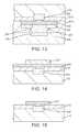
- FIG. 13is a sectional view of the exemplary embodiment of the semiconductor die depicting an exemplary mounting to a substrate
- FIG. 14is a sectional view of an alternate exemplary embodiment of a semiconductor die depicting passivation, metal layer and mask formation thereon;
- FIG. 15is a sectional view of the alternate exemplary embodiment of the semiconductor die depicting removal of the mask and portions of the metal layer;
- FIG. 16is a sectional view of the alternate exemplary embodiment of the semiconductor die depicting formation of an insulating layer thereon;
- FIG. 17is a sectional view of the alternate exemplary embodiment of the semiconductor die depicting formation of a conductor structure thereon;
- FIG. 18is a sectional view of the alternate exemplary embodiment of the semiconductor die depicting a reflow of the conductor structure
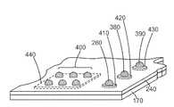
- FIG. 19is a pictorial view of another alternate exemplary embodiment of a semiconductor die provided with plural bump structures and a common metal layer;
- FIG. 20is an exploded pictorial view of an exemplary semiconductor die depicting exemplary mounting configurations.
- FIGS. 1-5therein is shown an exemplary conventional fabrication process for forming a conductive solder bump on the lower surface of a semiconductor chip 10 .
- FIGS. 1-5focus on a relatively small portion of a semiconductor device 10 .
- the semiconductor device 10includes two opposing sides 20 and 30 .
- the side 20is often referred to as a backside and the opposite side 30 is sometimes referred to as a front side.
- Active chip circuitry(not visible) is typically positioned in one or more layers proximate the front side 30 .
- a bond pad 40is provided proximate the side 30 and designed to provide an electrical pathway from the circuitry of the device 10 through a later-formed solder bump to establish electrical conductivity with circuitry external to the device 10 . There may be scores of such bond pads 40 depending on the complexity of the device 10 .
- a passivation layer 50 of silicon nitrideis formed on the side 30 and patterned so that an opening 60 extends to the bond pad 40 . The passivation layer 50 is designed to prevent the diffusion of metallic materials down into the semiconductor device 10 .
- a polyimide layer 70is formed on the stack consisting of the passivation layer 50 , the bond pad 40 and the semiconductor device 10 .
- the polyimide layer 70is formed with an opening 80 that is concentrically positioned with the opening 60 in the passivation layer 50 .
- Polyimideis chosen for its ability to provide both advantageous structural flexibility and electrical insulation.
- a metallization layer 90is formed on the polyimide layer 70 and down through the opening 80 therein to establish ohmic contact with the bond pad 40 .
- the metallization layer 90is sometimes referred to as an under bump metallization layer or UBM layer.
- the UBM layer 90is sometimes deposited as a sequential stack of different metallic materials, such as titanium copper and nickel.
- an insulating film 100is formed on the stack consisting of the metallization layer 90 , the polyimide layer 70 , the passivation layer 50 , the bond pad 40 and the device 10 .
- An opening 110is patterned in the film 100 that exposes a portion of the metallization layer 90 .
- the film 100is designed to serve as a mask, or a stencil if a stencil process is used, to enable the subsequent deposition of a conductor material in the opening 110 that will ultimately be fashioned into a solder bump.
- the opening 110is typically formed by a lithographic patterning process.
- the semiconductor device 10undergoes a plating process so that a conductor material 120 is deposited in the opening 110 of the film 100 and on the exposed portion of the metallization layer 90 .
- the conductor materialis typically a solder that establishes ohmic contact with the metallization layer 90 .
- a conventional solderconsists of a tin-lead mixture.
- a more recent innovationinvolves the use of a lead-free solder, such as a tin-copper solder.
- the polyimide layer 70 and the passivation layerinhibit diffusion of material from the conductor 120 and the metallization layer 90 into the device 10 .
- the bond pad 40is unaffected by the plating.
- the film 100 depicted in FIG. 4is removed and a thermal reflow process is performed on the semiconductor device 10 as depicted in FIG. 5 to reflow the conductor material 120 into a rounded bump.
- a thermal reflow processis performed on the semiconductor device 10 as depicted in FIG. 5 to reflow the conductor material 120 into a rounded bump.
- portions of the metallization layer 90 lateral to the solder bump 120are etched away by wet etching. At this point, an ohmic pathway exists between the solder bump 120 , the metallization layer 90 and the underlying bump pad 40 .
- the passivation layer 50 and the polyimide layer 70remain in place.
- FIG. 6depicts a sectional view of the semiconductor device 10 flip-chip mounted on another substrate 130 such that the side 30 faces downward.
- An underfill material 140is disposed between the polyimide layer 70 and the substrate 130 to lessen the stresses due to differences in the coefficients of thermal expansion of the electrical device 130 and the semiconductor device 10 .
- the solder bump of the semiconductor device 10is positioned on a corresponding bond pad 150 of the device 130 .
- an electrical pathwayis established between the bond pad 40 of the device 10 and the bond pad 150 of the device 130 via the metallization layer 90 and the solder bump 120 .
- a small portion of the solder bump 120 , the underfill layer 140 and the metallization layer 90is circumscribed by a small oval 160 .
- the portion circumscribed by the oval 160is shown at greater magnification in FIG. 7 .
- FIG. 7illustrates a drawback to the placement of the polyimide layer 70 shown in FIG. 6 between the metallization layer 90 and the solder bump 120 .
- a crack 160is shown in the solder bump 120 that extends from the border 165 with the underfill material 140 toward the central portion of the solder bump 120 .
- the crack 160is the result of thermal stresses that are not adequately compensated for by virtue of the relative stiffness of the lead-free solder bump 120 and the relative distance of the polyimide layer 70 from the area where the crack 160 forms.
- the crack 160may propagate across the entire width of the solder bump 120 and produce an open circuit.
- FIGS. 8-12depict successive sectional views of an integrated circuit or semiconductor device 170 undergoing various process steps leading to the formation of a solder bump. It should be understood that FIGS. 8-12 depict just a small portion of the device 170 .
- the semiconductor device 170may be any of a myriad of different types of circuit devices used in electronics, such as, for example, microprocessors, graphics processors, application specific integrated circuits, memory devices or the like, and may be single or multi-core.
- the device 170has opposing sides 180 and 190 .
- Device circuitryrepresented schematically by the dashed box 195 , may be located proximate the side 190 .
- the semiconductor device 170may be provided with multiple conductor or bond pads, one of which is shown and labeled 200 , that are positioned proximate the side 190 .
- the bond pad 200may be composed of a variety of conductor materials, such as aluminum, copper, silver, gold, titanium, refractory metals, refractory metal compounds, alloys of these or the like.
- the bond pad 200may be formed by plating, physical vapor deposition pr other material deposition techniques.
- a passivation layer 210is formed on the side 190 with an opening 220 .
- the passivation layer 210is designed to inhibit the diffusion of metallic or other materials down into the semiconductor device 170 .
- the layer 210may be composed of a variety of insulating materials, such as, for example, silicon nitride, silicon dioxide, various silicate glasses or the like.
- the opening 220may be formed by well-known lithographic patterning and etching techniques.
- a conductor or metal layer 230is formed on the passivation layer 210 and in the opening 220 thereof so that ohmic contact is established with the bond pad 200 .
- the metallization layer 230is designed to provide a conducting interface between the bond pad 200 and a subsequently formed solder structure (not shown).
- the metallization layer 230may be composed of a variety of conductor materials, such as aluminum, copper, silver, gold, titanium, refractory metals, refractory metal compounds, alloys of these or the like.
- the layer 230may consist of a laminate of plural metal layers, such as a titanium layer followed by a nickel-vanadium layer followed by a copper layer. In another embodiment, a titanium layer may be covered with a copper layer followed by a top coating of nickel.
- a great variety of conducting materialsmay be used for the metallization layer 230 .
- Various well-known techniques for applying metallic materialsmay be used, such as physical vapor deposition, chemical vapor deposition, plating or the like. It should be understood that additional conductor structures could be interposed between the metal layer 230 and the conductor pad 200 .
- An insulating film 240is deposited on the stack consisting of the metallization layer 230 , the passivation layer 210 , the pad 200 and the semiconductor device 170 .
- the insulating film 240is positioned on a surface 255 of the metal layer 230 .
- the layer 240is intended to provide passivation and cushion against differences in thermal expansion of the semiconductor device 170 , the metallization layer 230 and the subsequently formed solder bump (not shown).
- Exemplary materials for the insulating layer 240include, for example, polymeric materials such as polyimide and benzocyclobutene or the like, or other insulating materials such as silicon nitride or the like. Spin coating, chemical vapor deposition or other deposition processes may be used.
- the insulating layer 240is patterned lithographically with an opening 250 that exposes a portion of the metallization layer 230 . Note that the insulating layer 240 is positioned above the metallization layer 230 as opposed to below the metallization layer 90 in the conventional technique depicted in FIGS. 1-5 . This placement provides a structural advantage as described in more detail below.
- a mask film 260is deposited on the stack consisting of the insulating layer 240 , the metallization layer 230 , the passivation layer 210 , the pad 200 and the semiconductor device 170 .
- the mask film 260is patterned lithographically with an opening 270 that is concentric with the opening 250 in the insulating layer 240 . Together, the openings 250 and 270 leave a portion 275 of the surface 255 of the metal layer 230 exposed.
- a conductor materialis positioned in the combined openings 250 and 270 to establish ohmic contact with the metallization layer 230 and the underlying bond pad 200 of the device 170 .
- the film 260may be made from, for example, a rubberized epoxy resin with phenol resin, fused silica and synthetic rubber. Optionally, other materials suitable for a metal application mask may be used.
- the semiconductor device 170is subjected to a plating process to deposit a conductor material 280 in the openings 250 and 270 and on the exposed portion 275 of the surface 255 of the metallization layer 230 .
- the film 260serves as a mask against this deposition process.
- the conductor 280may be a lead-based solder or lead free as desired. Exemplary materials include, for example, tin-copper, tin-silver, or other solder materials.
- the conductor material 280borders the insulating layer 240 . At this point, a conductive pathway between the bond pad 200 , the metallization layer 230 and the conductor material 280 exists. The passivation layer 210 is unaffected. Of course, another conductor(s) (not shown) may be positioned between the conductor 280 and the bond pad 200 and still provide the desired ohmic pathway.
- the film 260 depicted in FIG. 11is removed and a reflow process is performed to reflow the conductor 280 into a ball or bump-like structure.
- the semiconductor device 170may be heated to about 170 to 190° C. for about 10 to 120 seconds.
- the appropriate parameters for the reflowwill depend on the composition of conductor material 280 .
- Unwanted portions of the metallization layer 230are removed by a chemical etch process. Thus, portions of the passivation layer 210 lateral to the conductor 280 are exposed.
- a conductive pathwayexists between the conductor 280 and the bump bond pad 200 by way of the metallization layer 230 .
- the conductor 280is positioned on a portion 285 of the insulating layer 240 .
- the portion 285provides a stress reducing interface with a peripheral corner 287 of the conductor 280 .
- FIG. 13depicts the semiconductor device 170 mounted on another electrical device 290 .
- the electrical device 290may be a printed circuit board, or other electrical device as desire.
- FIG. 13depicts a flip-chip mounting arrangement in which the device 170 is flipped over and mounted on the electrical device 290 so that the solder structure 280 is seated on a bond pad 300 of the electrical device 290 .
- the device 290may include scores of such pads 300 to receive corresponding bumps 280 of the device 170 .
- the pads 300may be fitted with small solder bumps (not shown) designed to meld with solder structure(s) 280 during a subsequent reflow.
- An underfill material 310is dispersed between the device 170 and the electrical device 290 to reduce the effects of differences in the coefficients of thermal expansion of the device 170 and the device 290 .
- the underfill 310may be, for example, an epoxy resin mixed with silica fillers and phenol resins. Because the insulating layer 240 is positioned between the metallization layer 230 and the solder structure 280 , an additional compliant cushioning effect is provided for the corner 320 of the solder bump 280 against the types of thermal stresses and cracking associated with the conventional structure depicted in FIGS. 6 and 7 . Note that the corner 320 extends around the entire periphery of the solder structure 280 .
- a plating processmay be used to form the solder structures 280 .
- a stencil processmay be used to establish a solder structure.
- the semiconductor device 170may be processed as described elsewhere herein to provide the bond pad 200 , the passivation layer 210 and the metallization layer 230 .
- an etch mask 330 of resist or other mask materialis formed on the metallization layer 230 , and an etch is performed on the metallization layer 230 to trim portions thereof lateral to the bond pad 200 and expose portions of the passivation layer 210 as shown in FIG. 15 .
- the etch mask 330may be removed by ashing, solvent stripping or the like.
- the metallization layer 230may be circular or another shape as desired.
- the bond pad 200is unaffected by the etch or mask strip.
- the insulating layer 240is formed on the stack consisting of the metallization layer 230 , the passivation layer 210 , the bond pad 200 and the semiconductor device 170 as generally described elsewhere herein.
- the insulating layer 240has the aforementioned opening 250 leading to the metallization layer 230 and leaving the surface thereof 255 with an exposed portion 275 .
- a stencil 340is formed on the stack consisting of the insulating layer 240 , the metallization layer 230 , the passivation layer 210 , the bond pad 200 and the semiconductor device 170 .
- the stencil 340includes an opening 350 over the metallization layer 230 and portions of the insulating layer 240 .
- the stencil 340may be fabricated from, for example, a rubberized epoxy resin with phenol resin, fused silica and synthetic rubber. Optionally, other materials suitable for metal application stencils may be used.
- a conductor paste 360is pressed into the opening 350 of the stencil 340 .
- the conductor paste 360is positioned on the exposed portion 275 of the surface 255 of the metal layer 230 and a portion 365 of the insulating layer 240 .
- the paste 360may be composed of the same materials used for the solder bump 280 described elsewhere herein.
- another conductor(s)(not shown) may be positioned between the conductor 360 and the bond pad 200 and still provide the desired ohmic pathway.
- the stencil 340is removed and a thermal reflow process is performed to reshape the conductor paste 360 into a bump that metallurgically bonds to the pad 200 as shown in FIG. 18 .
- the semiconductor device 170may be heated to about 170 to 190° C. for about 10 to 120 seconds.
- the appropriate parameters for the reflowwill depend on the composition of conductor paste 360 .
- the passivation layer 210is unaffected.
- the conductor 360is positioned on a portion 365 of the insulating layer 240 . As in the above-described embodiment, the insulating layer 240 provides enhanced structural protection for a peripheral corner 370 of the solder bump 360 .
- FIG. 19is a pictorial view of a portion of the semiconductor device 170 positioned with the insulating layer 240 and several bumps facing upwardly.
- One of the bumpsis labeled 280 as in FIGS. 8-12 .
- Two other bumpsare separately labeled 380 and 390 .
- a group of six bumpsare collectively labeled 400 .
- the bumps 280 , 380 and 390may be formed and provided with discrete under bump conductor structures or metal layers 410 , 420 and 430 that are structurally isolated using the techniques disclosed herein.
- the metal layers 410 , 420 and 430are covered by the insulating layer 240 and thus shown in phantom.
- the group of bumps 400may be formed using the techniques disclosed herein, but with a common under bump conductor structure or metal layer 440 that is covered by the insulating layer 240 and thus also shown in phantom.
- the insulating layer 240is thus formed with plural openings to expose plural portions of the metal layer 440 prior to formation of the bumps 400 .
- the metal layer 440can serve as a routing structure for the group of bumps 400 . This may be advantageous where several bumps are dedicated temporarily or permanently to one type of input/output, such as power or ground. Because the insulating layer 240 is positioned between the group 400 of bumps and the metallization layer 440 , selected bumps can be tied together without risk that solder will seep laterally and make unwanted shorts during reflow. Of course, the number and groupings of bumps and shaping of the common under bump metallization layer(s) 440 are subject to great variation.
- the semiconductor device 170may be mounted in a variety of ways.
- FIG. 20depicts an exploded pictorial view of a few exemplary mounting possibilities.
- the semiconductor device 170is depicted with the solder bumps 280 facing upwards.
- the device 170may be flipped over as indicated by the arrow 450 and flip-chip mounted on a substrate 460 .
- the substrate 460may be a package substrate, a printed circuit board or other type of substrate. If configured as a package substrate, the substrate 460 may be a pin grid array, a ball grid array, a land grid array, a surface mount or other type configuration.
- the substrate 460may be mounted to another substrate 470 .
- the substrate 470may be a printed circuit board or other type of substrate.
- the substrate 470may be a motherboard for a computer system.
- the semiconductor device 170may be included in a larger system, such as a computing device represented by the dashed box 480 .
- the computing device 480may be include, for example, a digital television, a handheld mobile device, a personal computer, a server, a memory device, an add-in board such as a graphics card, or any other computing device employing semiconductors.
Landscapes
- Engineering & Computer Science (AREA)
- Computer Hardware Design (AREA)
- Microelectronics & Electronic Packaging (AREA)
- Power Engineering (AREA)
- Physics & Mathematics (AREA)
- Condensed Matter Physics & Semiconductors (AREA)
- General Physics & Mathematics (AREA)
- Manufacturing & Machinery (AREA)
- Internal Circuitry In Semiconductor Integrated Circuit Devices (AREA)
- Wire Bonding (AREA)
Abstract
Description
Claims (15)
Priority Applications (1)
| Application Number | Priority Date | Filing Date | Title |
|---|---|---|---|
| US13/027,076US8294266B2 (en) | 2007-08-01 | 2011-02-14 | Conductor bump method and apparatus |
Applications Claiming Priority (2)
| Application Number | Priority Date | Filing Date | Title |
|---|---|---|---|
| US11/832,486US7906424B2 (en) | 2007-08-01 | 2007-08-01 | Conductor bump method and apparatus |
| US13/027,076US8294266B2 (en) | 2007-08-01 | 2011-02-14 | Conductor bump method and apparatus |
Related Parent Applications (1)
| Application Number | Title | Priority Date | Filing Date |
|---|---|---|---|
| US11/832,486DivisionUS7906424B2 (en) | 2007-08-01 | 2007-08-01 | Conductor bump method and apparatus |
Publications (2)
| Publication Number | Publication Date |
|---|---|
| US20110133338A1 US20110133338A1 (en) | 2011-06-09 |
| US8294266B2true US8294266B2 (en) | 2012-10-23 |
Family
ID=40035683
Family Applications (2)
| Application Number | Title | Priority Date | Filing Date |
|---|---|---|---|
| US11/832,486Active2029-04-22US7906424B2 (en) | 2007-08-01 | 2007-08-01 | Conductor bump method and apparatus |
| US13/027,076ActiveUS8294266B2 (en) | 2007-08-01 | 2011-02-14 | Conductor bump method and apparatus |
Family Applications Before (1)
| Application Number | Title | Priority Date | Filing Date |
|---|---|---|---|
| US11/832,486Active2029-04-22US7906424B2 (en) | 2007-08-01 | 2007-08-01 | Conductor bump method and apparatus |
Country Status (2)
| Country | Link |
|---|---|
| US (2) | US7906424B2 (en) |
| WO (1) | WO2009016495A1 (en) |
Families Citing this family (7)
| Publication number | Priority date | Publication date | Assignee | Title |
|---|---|---|---|---|
| US7906424B2 (en) | 2007-08-01 | 2011-03-15 | Advanced Micro Devices, Inc. | Conductor bump method and apparatus |
| US8776335B2 (en) | 2010-11-17 | 2014-07-15 | General Electric Company | Methods of fabricating ultrasonic transducer assemblies |
| US20120326299A1 (en)* | 2011-06-24 | 2012-12-27 | Topacio Roden R | Semiconductor chip with dual polymer film interconnect structures |
| KR101940237B1 (en)* | 2012-06-14 | 2019-01-18 | 한국전자통신연구원 | Method for Manufacturing Solder on Pad on Fine Pitch PCB Substrate and Flip Chip Bonding Method of Semiconductor Using The Same |
| US9013039B2 (en)* | 2013-08-05 | 2015-04-21 | Globalfoundries Inc. | Wafer support system for 3D packaging |
| US20170356640A1 (en)* | 2016-06-10 | 2017-12-14 | Innotec, Corp. | Illumination assembly including thermal energy management |
| WO2020174670A1 (en)* | 2019-02-28 | 2020-09-03 | 三菱電機株式会社 | Semiconductor device and manufacturing method for semiconductor device |
Citations (69)
| Publication number | Priority date | Publication date | Assignee | Title |
|---|---|---|---|---|
| US1194995A (en) | 1916-08-15 | Ella m | ||
| GB1149569A (en) | 1966-09-01 | 1969-04-23 | Mini Of Technology | Capacitors and methods for their manufacture |
| US3593319A (en) | 1968-12-23 | 1971-07-13 | Gen Electric | Card-changeable capacitor read-only memory |
| DE2548563A1 (en) | 1975-10-30 | 1977-05-05 | Licentia Gmbh | Capacitor for integrated semiconductor circuits - formed by metal pattern on insulation covering silicon substrate |
| US4249196A (en) | 1978-08-21 | 1981-02-03 | Burroughs Corporation | Integrated circuit module with integral capacitor |
| US4409608A (en) | 1981-04-28 | 1983-10-11 | The United States Of America As Represented By The Secretary Of The Navy | Recessed interdigitated integrated capacitor |
| US4434452A (en) | 1980-01-18 | 1984-02-28 | Matsushita Electric Industrial Co., Ltd. | Metallized film capacitor |
| US4470098A (en) | 1982-02-18 | 1984-09-04 | Itt Industries, Inc. | Multilayer ceramic dielectric capacitors |
| JPS61259560A (en) | 1985-05-14 | 1986-11-17 | Nec Corp | Semiconductor integrated circuit |
| JPS61263251A (en) | 1985-05-17 | 1986-11-21 | Nec Corp | Semiconductor device |
| US4685197A (en) | 1986-01-07 | 1987-08-11 | Texas Instruments Incorporated | Fabricating a stacked capacitor |
| EP0246808A1 (en) | 1986-05-16 | 1987-11-25 | Showa Denko Kabushiki Kaisha | Solid electrolytic capacitor |
| JPS6484616A (en) | 1987-09-28 | 1989-03-29 | Toshiba Corp | Condenser |
| JPH0196943A (en) | 1987-10-09 | 1989-04-14 | Toshiba Corp | Semiconductor integrated circuit device |
| US4866567A (en) | 1989-01-06 | 1989-09-12 | Ncr Corporation | High frequency integrated circuit channel capacitor |
| US4868613A (en) | 1985-04-05 | 1989-09-19 | Fujitsu Limited | Microwave monolithic integrated circuit device |
| EP0347853A2 (en) | 1988-06-21 | 1989-12-27 | Sanyo Electric Co., Ltd. | Semiconductor integrated circuit |
| US4901128A (en) | 1982-11-04 | 1990-02-13 | Hitachi, Ltd. | Semiconductor memory |
| US4914546A (en) | 1989-02-03 | 1990-04-03 | Micrel Incorporated | Stacked multi-polysilicon layer capacitor |
| US4937649A (en) | 1986-09-12 | 1990-06-26 | Nec Corporation | Semiconductor integrated circuit having a capacitor for stabilizing a voltage at a power supplying wiring |
| JPH02231755A (en) | 1989-03-03 | 1990-09-13 | Mitsubishi Electric Corp | Monolithic integrated circuit having mim capacitor |
| US5053916A (en) | 1989-03-13 | 1991-10-01 | U.S. Philips Corporation | Surface-mounted multilayer capacitor and printed circuit board having such a multilayer capacitor |
| US5081559A (en) | 1991-02-28 | 1992-01-14 | Micron Technology, Inc. | Enclosed ferroelectric stacked capacitor |
| US5089878A (en) | 1989-06-09 | 1992-02-18 | Lee Jaesup N | Low impedance packaging |
| JPH04268756A (en) | 1991-02-25 | 1992-09-24 | Mitsubishi Electric Corp | Capacitor of integrated circuit |
| US5155658A (en) | 1992-03-05 | 1992-10-13 | Bell Communications Research, Inc. | Crystallographically aligned ferroelectric films usable in memories and method of crystallographically aligning perovskite films |
| US5162258A (en) | 1988-10-17 | 1992-11-10 | Lemnios Zachary J | Three metal personalization of application specific monolithic microwave integrated circuit |
| US5189594A (en) | 1991-09-20 | 1993-02-23 | Rohm Co., Ltd. | Capacitor in a semiconductor integrated circuit and non-volatile memory using same |
| US5208725A (en) | 1992-08-19 | 1993-05-04 | Akcasu Osman E | High capacitance structure in a semiconductor device |
| US5656863A (en) | 1993-02-18 | 1997-08-12 | Mitsubishi Denki Kabushiki Kaisha | Resin seal semiconductor package |
| US5668399A (en) | 1995-02-08 | 1997-09-16 | International Business Machines Corporation | Semiconductor device with increased on chip decoupling capacitance |
| US5907785A (en) | 1995-08-24 | 1999-05-25 | International Business Machines Corporation | Wafer with elevated contact substructures |
| JP2000031188A (en) | 1998-07-13 | 2000-01-28 | Nec Corp | Bump arrangement method of flip-chip integrated circuit and the flip-chip integrated circuit |
| US6266227B1 (en) | 1998-08-26 | 2001-07-24 | Kyocera Corporation | Thin-film capacitor |
| US6384343B1 (en) | 1999-12-03 | 2002-05-07 | Nec Corporation | Semiconductor device |
| US6387795B1 (en)* | 2001-03-22 | 2002-05-14 | Apack Technologies Inc. | Wafer-level packaging |
| US20020070451A1 (en)* | 2000-12-08 | 2002-06-13 | Burnette Terry E. | Semiconductor device having a ball grid array and method therefor |
| US6433427B1 (en)* | 2001-01-16 | 2002-08-13 | Industrial Technology Research Institute | Wafer level package incorporating dual stress buffer layers for I/O redistribution and method for fabrication |
| US20030001287A1 (en)* | 2001-06-27 | 2003-01-02 | Intel Corporation | Flexible tape electronics packaging |
| US20030071300A1 (en) | 2001-03-30 | 2003-04-17 | Yukihiko Yashima | Tunable thin film capacitor |
| US6617655B1 (en)* | 2002-04-05 | 2003-09-09 | Fairchild Semiconductor Corporation | MOSFET device with multiple gate contacts offset from gate contact area and over source area |
| US6656828B1 (en) | 1999-01-22 | 2003-12-02 | Hitachi, Ltd. | Method of forming bump electrodes |
| US20040056351A1 (en) | 2002-09-20 | 2004-03-25 | Himax Technologies, Inc. | Semiconductor device and manufacturing method thereof |
| US20040070042A1 (en)* | 2002-10-15 | 2004-04-15 | Megic Corporation | Method of wire bonding over active area of a semiconductor circuit |
| US20040104451A1 (en) | 2002-10-29 | 2004-06-03 | Kiyoshi Ooi | Capacitor and manufacturing method thereof, semiconductor device and substrate for a semiconductor device |
| US20040188851A1 (en) | 2003-03-26 | 2004-09-30 | Nec Electronics Corporation | Semiconductor device and method for manufacturing same |
| US20050006688A1 (en) | 2001-12-04 | 2005-01-13 | Solo De Zaldivar Jose | Arrangement comprising a capacitor |
| US20050121804A1 (en) | 2003-12-08 | 2005-06-09 | Nick Kuo | Chip structure with bumps and testing pads |
| US6929976B2 (en) | 2001-06-21 | 2005-08-16 | Ati Technologies, Inc. | Multi-die module and method thereof |
| US6937458B2 (en) | 2001-02-23 | 2005-08-30 | Intel Corporation | Selectable decoupling capacitors for integrated circuit and methods of use |
| US20050280034A1 (en) | 2004-06-02 | 2005-12-22 | Fujitsu Limited | Semiconductor device |
| US20060033197A1 (en) | 2001-10-30 | 2006-02-16 | Intel Corporation | Power gridding scheme |
| US20060051952A1 (en) | 2004-09-09 | 2006-03-09 | Phoenix Precision Technology Corporation | Method for fabricating conductive bump of circuit board |
| WO2006050127A2 (en) | 2004-10-29 | 2006-05-11 | Flipchip International, Llc | Semiconductor device package with bump overlying a polymer layer |
| JP2006203261A (en) | 2006-04-26 | 2006-08-03 | Renesas Technology Corp | Semiconductor apparatus |
| US7112884B2 (en) | 2002-08-23 | 2006-09-26 | Ati Technologies, Inc. | Integrated circuit having memory disposed thereon and method of making thereof |
| WO2006129832A1 (en) | 2005-06-01 | 2006-12-07 | Casio Computer Co., Ltd. | Semiconductor device and mounting structure thereof |
| US7161793B2 (en) | 2002-11-14 | 2007-01-09 | Fujitsu Limited | Layer capacitor element and production process as well as electronic device |
| US20070052095A1 (en) | 2005-09-06 | 2007-03-08 | Katsuhiro Torii | Semiconductor device and manufacturing method thereof |
| US20070069347A1 (en) | 2005-09-23 | 2007-03-29 | Mou-Shiung Lin | Semiconductor chip and process for forming the same |
| US7227736B2 (en) | 2002-08-19 | 2007-06-05 | Fujitsu Limited | Capacitor device and method of manufacturing the same |
| US20070132095A1 (en)* | 2005-12-09 | 2007-06-14 | Stmicroelectronics S.A. | Integrated circuit chip with external pads and process for fabricating such a chip |
| US20070170587A1 (en) | 2006-01-24 | 2007-07-26 | Denso Corporation | Ball grid array |
| US20070176292A1 (en) | 2006-01-27 | 2007-08-02 | Taiwan Semiconductor Manufacturing Co., Ltd. | Bonding pad structure |
| US7364998B2 (en)* | 2005-07-21 | 2008-04-29 | Taiwan Semiconductor Manufacturing Co., Ltd. | Method for forming high reliability bump structure |
| US20080146019A1 (en) | 2001-12-13 | 2008-06-19 | Megica Corporation | Chip structure and process for forming the same |
| US20080153204A1 (en) | 2002-07-31 | 2008-06-26 | Micron Technology, Inc. | Semiconductor dice having back side redistribution layer accessed using through-silicon vias, methods |
| JP4268756B2 (en) | 1997-12-04 | 2009-05-27 | ビーエーエスエフ ソシエタス・ヨーロピア | Method for producing chlorocarboxylic acid chloride |
| US7906424B2 (en) | 2007-08-01 | 2011-03-15 | Advanced Micro Devices, Inc. | Conductor bump method and apparatus |
Family Cites Families (1)
| Publication number | Priority date | Publication date | Assignee | Title |
|---|---|---|---|---|
| JPS5991718A (en) | 1982-11-16 | 1984-05-26 | Elmec Corp | Electromagnetic delay line |
- 2007
- 2007-08-01USUS11/832,486patent/US7906424B2/enactiveActive
- 2008
- 2008-08-01WOPCT/IB2008/002024patent/WO2009016495A1/enactiveApplication Filing
- 2011
- 2011-02-14USUS13/027,076patent/US8294266B2/enactiveActive
Patent Citations (71)
| Publication number | Priority date | Publication date | Assignee | Title |
|---|---|---|---|---|
| US1194995A (en) | 1916-08-15 | Ella m | ||
| GB1149569A (en) | 1966-09-01 | 1969-04-23 | Mini Of Technology | Capacitors and methods for their manufacture |
| US3593319A (en) | 1968-12-23 | 1971-07-13 | Gen Electric | Card-changeable capacitor read-only memory |
| DE2548563A1 (en) | 1975-10-30 | 1977-05-05 | Licentia Gmbh | Capacitor for integrated semiconductor circuits - formed by metal pattern on insulation covering silicon substrate |
| US4249196A (en) | 1978-08-21 | 1981-02-03 | Burroughs Corporation | Integrated circuit module with integral capacitor |
| US4434452A (en) | 1980-01-18 | 1984-02-28 | Matsushita Electric Industrial Co., Ltd. | Metallized film capacitor |
| US4409608A (en) | 1981-04-28 | 1983-10-11 | The United States Of America As Represented By The Secretary Of The Navy | Recessed interdigitated integrated capacitor |
| US4470098A (en) | 1982-02-18 | 1984-09-04 | Itt Industries, Inc. | Multilayer ceramic dielectric capacitors |
| US4901128A (en) | 1982-11-04 | 1990-02-13 | Hitachi, Ltd. | Semiconductor memory |
| US4868613A (en) | 1985-04-05 | 1989-09-19 | Fujitsu Limited | Microwave monolithic integrated circuit device |
| JPS61259560A (en) | 1985-05-14 | 1986-11-17 | Nec Corp | Semiconductor integrated circuit |
| JPS61263251A (en) | 1985-05-17 | 1986-11-21 | Nec Corp | Semiconductor device |
| US4685197A (en) | 1986-01-07 | 1987-08-11 | Texas Instruments Incorporated | Fabricating a stacked capacitor |
| US4797789A (en) | 1986-05-16 | 1989-01-10 | Showa Denko Kabushiki Kaisha | Solid electrolytic capacitor |
| EP0246808A1 (en) | 1986-05-16 | 1987-11-25 | Showa Denko Kabushiki Kaisha | Solid electrolytic capacitor |
| US4937649A (en) | 1986-09-12 | 1990-06-26 | Nec Corporation | Semiconductor integrated circuit having a capacitor for stabilizing a voltage at a power supplying wiring |
| JPS6484616A (en) | 1987-09-28 | 1989-03-29 | Toshiba Corp | Condenser |
| JPH0196943A (en) | 1987-10-09 | 1989-04-14 | Toshiba Corp | Semiconductor integrated circuit device |
| EP0347853A2 (en) | 1988-06-21 | 1989-12-27 | Sanyo Electric Co., Ltd. | Semiconductor integrated circuit |
| US5162258A (en) | 1988-10-17 | 1992-11-10 | Lemnios Zachary J | Three metal personalization of application specific monolithic microwave integrated circuit |
| US4866567A (en) | 1989-01-06 | 1989-09-12 | Ncr Corporation | High frequency integrated circuit channel capacitor |
| US4914546A (en) | 1989-02-03 | 1990-04-03 | Micrel Incorporated | Stacked multi-polysilicon layer capacitor |
| JPH02231755A (en) | 1989-03-03 | 1990-09-13 | Mitsubishi Electric Corp | Monolithic integrated circuit having mim capacitor |
| US5053916A (en) | 1989-03-13 | 1991-10-01 | U.S. Philips Corporation | Surface-mounted multilayer capacitor and printed circuit board having such a multilayer capacitor |
| US5089878A (en) | 1989-06-09 | 1992-02-18 | Lee Jaesup N | Low impedance packaging |
| JPH04268756A (en) | 1991-02-25 | 1992-09-24 | Mitsubishi Electric Corp | Capacitor of integrated circuit |
| JP2700959B2 (en) | 1991-02-25 | 1998-01-21 | 三菱電機株式会社 | Integrated circuit capacitors |
| US5081559A (en) | 1991-02-28 | 1992-01-14 | Micron Technology, Inc. | Enclosed ferroelectric stacked capacitor |
| US5189594A (en) | 1991-09-20 | 1993-02-23 | Rohm Co., Ltd. | Capacitor in a semiconductor integrated circuit and non-volatile memory using same |
| US5155658A (en) | 1992-03-05 | 1992-10-13 | Bell Communications Research, Inc. | Crystallographically aligned ferroelectric films usable in memories and method of crystallographically aligning perovskite films |
| US5208725A (en) | 1992-08-19 | 1993-05-04 | Akcasu Osman E | High capacitance structure in a semiconductor device |
| US5656863A (en) | 1993-02-18 | 1997-08-12 | Mitsubishi Denki Kabushiki Kaisha | Resin seal semiconductor package |
| US5668399A (en) | 1995-02-08 | 1997-09-16 | International Business Machines Corporation | Semiconductor device with increased on chip decoupling capacitance |
| US5907785A (en) | 1995-08-24 | 1999-05-25 | International Business Machines Corporation | Wafer with elevated contact substructures |
| JP4268756B2 (en) | 1997-12-04 | 2009-05-27 | ビーエーエスエフ ソシエタス・ヨーロピア | Method for producing chlorocarboxylic acid chloride |
| JP2000031188A (en) | 1998-07-13 | 2000-01-28 | Nec Corp | Bump arrangement method of flip-chip integrated circuit and the flip-chip integrated circuit |
| US6266227B1 (en) | 1998-08-26 | 2001-07-24 | Kyocera Corporation | Thin-film capacitor |
| US6656828B1 (en) | 1999-01-22 | 2003-12-02 | Hitachi, Ltd. | Method of forming bump electrodes |
| US6384343B1 (en) | 1999-12-03 | 2002-05-07 | Nec Corporation | Semiconductor device |
| US20020070451A1 (en)* | 2000-12-08 | 2002-06-13 | Burnette Terry E. | Semiconductor device having a ball grid array and method therefor |
| US6433427B1 (en)* | 2001-01-16 | 2002-08-13 | Industrial Technology Research Institute | Wafer level package incorporating dual stress buffer layers for I/O redistribution and method for fabrication |
| US6937458B2 (en) | 2001-02-23 | 2005-08-30 | Intel Corporation | Selectable decoupling capacitors for integrated circuit and methods of use |
| US6387795B1 (en)* | 2001-03-22 | 2002-05-14 | Apack Technologies Inc. | Wafer-level packaging |
| US20030071300A1 (en) | 2001-03-30 | 2003-04-17 | Yukihiko Yashima | Tunable thin film capacitor |
| US6929976B2 (en) | 2001-06-21 | 2005-08-16 | Ati Technologies, Inc. | Multi-die module and method thereof |
| US20030001287A1 (en)* | 2001-06-27 | 2003-01-02 | Intel Corporation | Flexible tape electronics packaging |
| US20060033197A1 (en) | 2001-10-30 | 2006-02-16 | Intel Corporation | Power gridding scheme |
| US20050006688A1 (en) | 2001-12-04 | 2005-01-13 | Solo De Zaldivar Jose | Arrangement comprising a capacitor |
| US20080146019A1 (en) | 2001-12-13 | 2008-06-19 | Megica Corporation | Chip structure and process for forming the same |
| US6617655B1 (en)* | 2002-04-05 | 2003-09-09 | Fairchild Semiconductor Corporation | MOSFET device with multiple gate contacts offset from gate contact area and over source area |
| US20080153204A1 (en) | 2002-07-31 | 2008-06-26 | Micron Technology, Inc. | Semiconductor dice having back side redistribution layer accessed using through-silicon vias, methods |
| US7227736B2 (en) | 2002-08-19 | 2007-06-05 | Fujitsu Limited | Capacitor device and method of manufacturing the same |
| US7112884B2 (en) | 2002-08-23 | 2006-09-26 | Ati Technologies, Inc. | Integrated circuit having memory disposed thereon and method of making thereof |
| US20040056351A1 (en) | 2002-09-20 | 2004-03-25 | Himax Technologies, Inc. | Semiconductor device and manufacturing method thereof |
| US20040070042A1 (en)* | 2002-10-15 | 2004-04-15 | Megic Corporation | Method of wire bonding over active area of a semiconductor circuit |
| US20040104451A1 (en) | 2002-10-29 | 2004-06-03 | Kiyoshi Ooi | Capacitor and manufacturing method thereof, semiconductor device and substrate for a semiconductor device |
| US7161793B2 (en) | 2002-11-14 | 2007-01-09 | Fujitsu Limited | Layer capacitor element and production process as well as electronic device |
| US20040188851A1 (en) | 2003-03-26 | 2004-09-30 | Nec Electronics Corporation | Semiconductor device and method for manufacturing same |
| US20050121804A1 (en) | 2003-12-08 | 2005-06-09 | Nick Kuo | Chip structure with bumps and testing pads |
| US20050280034A1 (en) | 2004-06-02 | 2005-12-22 | Fujitsu Limited | Semiconductor device |
| US20060051952A1 (en) | 2004-09-09 | 2006-03-09 | Phoenix Precision Technology Corporation | Method for fabricating conductive bump of circuit board |
| WO2006050127A2 (en) | 2004-10-29 | 2006-05-11 | Flipchip International, Llc | Semiconductor device package with bump overlying a polymer layer |
| WO2006129832A1 (en) | 2005-06-01 | 2006-12-07 | Casio Computer Co., Ltd. | Semiconductor device and mounting structure thereof |
| US7364998B2 (en)* | 2005-07-21 | 2008-04-29 | Taiwan Semiconductor Manufacturing Co., Ltd. | Method for forming high reliability bump structure |
| US20070052095A1 (en) | 2005-09-06 | 2007-03-08 | Katsuhiro Torii | Semiconductor device and manufacturing method thereof |
| US20070069347A1 (en) | 2005-09-23 | 2007-03-29 | Mou-Shiung Lin | Semiconductor chip and process for forming the same |
| US20070132095A1 (en)* | 2005-12-09 | 2007-06-14 | Stmicroelectronics S.A. | Integrated circuit chip with external pads and process for fabricating such a chip |
| US20070170587A1 (en) | 2006-01-24 | 2007-07-26 | Denso Corporation | Ball grid array |
| US20070176292A1 (en) | 2006-01-27 | 2007-08-02 | Taiwan Semiconductor Manufacturing Co., Ltd. | Bonding pad structure |
| JP2006203261A (en) | 2006-04-26 | 2006-08-03 | Renesas Technology Corp | Semiconductor apparatus |
| US7906424B2 (en) | 2007-08-01 | 2011-03-15 | Advanced Micro Devices, Inc. | Conductor bump method and apparatus |
Non-Patent Citations (28)
| Title |
|---|
| C. Kortekaas; On-chip Quasi-static Floating-gate Capacitance Measurement Method; Proc. IEEE 1990 Int. Conference on Microelectric Test Structures; vol. 3; Mar. 1990; pp. 109-113. |
| Chi Hou Chan et al.; Analysis of MMIC Structures Using an Efficient Iterative Approach; IEEE Transactions on Microwave Theory and Techniques; vol. 36; No. 1; Jan. 1988; pp. 96-105. |
| Gary D. Alley; Interdigital Capacitors and Their Application to Lumped-Element Microwave Integrated Circuits; IEEE Transactions on Microwave Theory and Techniques; Dec. 1970; pp. 1028-1033. |
| Ingo Wolff et al.; Computer Models for MMIC Capacitors and Inductors; pp. 853-858, 1988. |
| Jae-Kyung Wee et al.; An Antifuse EPROM Circuitry Scheme for Field-Programmable Repair in DRAM; IEEE Journal of Solid-State Circuits, vol. 35, No. 10, Oct. 2000; pp. 1408-1414. |
| John L. Hobdell; Optimization of Interdigital Capacitors; IEEE Transactions on Microwave Theory and Techniques, vol. MIT-27; No. 9; Sep. 1979; pp. 788-791. |
| Myles H. Wakayama et al.; A 30-MHz Low-Jitter High-Linearity CMOS Voltage-Controlled Oscillator; IEEE Journal of Solid-State Circuits; vol. SC-22; No. 6; Dec. 1987; pp. 1074-1081. |
| PCT/CA2009/001039 International Search Report mailed Oct. 16, 2009. |
| PCT/IB2008/002024 International Search Report, 2008. |
| PCT/IB2008/003343 International Search Report, 2008. |
| Reza Esfandiari et al.; Design of Interdigitated Capacitors and Their Application to Gallium Arsenide Monolithic Filters; IEEE Transactions on Microwave Theory and Techniques; vol. 31; No. 1; Jan. 1983; pp. 57-64. |
| T. Ema et al.; 3-Dimensional Stacked Capacitor Cell for 16M and 64M Drams; 1988 IEEE; pp. 592-595. |
| Tirdad Sowlati et al.; High Density Capacitance Structures in Submicron CMOS for Low Power RF Applications; ISLPED '01, Aug. 6-7, 2001; pp. 243-246. |
| U.S. Appl. No. 12/180,042, filed Jul. 25, 2008, Roden R. Topacio et al. |
| USPTO 2nd Notice of Allowance notification date Jun. 8, 2012; U.S. Appl. No. 12/180,042. |
| USPTO Notice of Allowance notification date Apr. 4, 2012; U.S. Appl. No. 12/180,042. |
| USPTO Notice of Allowance notification date Nov. 8, 2010; U.S. Appl. No. 11/832,486. |
| USPTO Office Action mailed Apr. 1, 2010; U.S. Appl. No. 11/949,951. |
| USPTO Office Action notification date Apr. 1, 2010; U.S. Appl. No. 11/949,951. |
| USPTO Office Action notification date Aug. 18, 2010; U.S. Appl. No. 11/832,486. |
| USPTO Office Action notification date Aug. 18, 2010; U.S. Appl. No. 12/180,042. |
| USPTO Office Action notification date Feb. 1, 2011; U.S. Appl. No. 11/949,951. |
| USPTO Office Action notification date Jan. 3, 2011; U.S. Appl. No. 12/180,042. |
| USPTO Office Action notification date Jul. 12, 2010; U.S. Appl. No. 11/832,486. |
| USPTO Office Action notification date Jul. 8, 2011; U.S. Appl. No. 11/949,951. |
| USPTO Office Action notification date Mar. 8, 2010; U.S. Appl. No. 11/832,486. |
| USPTO Office Action notification date Nov. 8, 2011; U.S. Appl. No. 12/180,042. |
| Wikipedia; Benzocyclobutene; http://en.wikipedia.org/wiki/Benzocyclobutene; Jun. 2007. |
Also Published As
| Publication number | Publication date |
|---|---|
| WO2009016495A1 (en) | 2009-02-05 |
| US20110133338A1 (en) | 2011-06-09 |
| US20090032940A1 (en) | 2009-02-05 |
| US7906424B2 (en) | 2011-03-15 |
Similar Documents
| Publication | Publication Date | Title |
|---|---|---|
| EP2229694B1 (en) | Semiconductor chip under-bump metallization structure and manufacturing method thereof | |
| CN100385642C (en) | Pad redistribution layer and method for fabricating copper pad redistribution layer | |
| US6455408B1 (en) | Method for manufacturing semiconductor devices having redistribution patterns with a concave pattern in a bump pad area | |
| TWI431744B (en) | Semiconductor device and method for making same | |
| JP4131595B2 (en) | Manufacturing method of semiconductor device | |
| US7969020B2 (en) | Die stacking apparatus and method | |
| US8211789B2 (en) | Manufacturing method of a bump structure having a reinforcement member | |
| US8294266B2 (en) | Conductor bump method and apparatus | |
| US8647974B2 (en) | Method of fabricating a semiconductor chip with supportive terminal pad | |
| US20160233194A1 (en) | Package structure and fabrication method thereof | |
| US20130341785A1 (en) | Semiconductor chip with expansive underbump metallization structures | |
| US20150228594A1 (en) | Via under the interconnect structures for semiconductor devices | |
| US20130256871A1 (en) | Semiconductor chip device with fragmented solder structure pads | |
| US20120326299A1 (en) | Semiconductor chip with dual polymer film interconnect structures | |
| US6649507B1 (en) | Dual layer photoresist method for fabricating a mushroom bumping plating structure | |
| JP3678239B2 (en) | Semiconductor device and manufacturing method thereof, circuit board, and electronic apparatus | |
| US11515274B2 (en) | Semiconductor package and manufacturing method thereof | |
| US20120261812A1 (en) | Semiconductor chip with patterned underbump metallization | |
| US20110057307A1 (en) | Semiconductor Chip with Stair Arrangement Bump Structures | |
| JP3424164B2 (en) | Manufacturing method of semiconductor device | |
| US20250149488A1 (en) | Bonding scheme for semiconductor packaging | |
| JP2005064228A (en) | Electronic component and manufacturing method thereof | |
| JP2005064227A (en) | Electronic component and manufacturing method thereof | |
| JP2006128158A (en) | Semiconductor device and method for manufacturing the same, wiring substrate and method for manufacturing the same | |
| JP2003045908A (en) | Semiconductor device and manufacturing method thereof |
Legal Events
| Date | Code | Title | Description |
|---|---|---|---|
| FEPP | Fee payment procedure | Free format text:PAYOR NUMBER ASSIGNED (ORIGINAL EVENT CODE: ASPN); ENTITY STATUS OF PATENT OWNER: LARGE ENTITY | |
| STCF | Information on status: patent grant | Free format text:PATENTED CASE | |
| AS | Assignment | Owner name:ADVANCED MICRO DEVICES, INC., CALIFORNIA Free format text:ASSIGNMENT OF ASSIGNORS INTEREST;ASSIGNOR:ATI TECHNOLOGIES ULC;REEL/FRAME:037792/0969 Effective date:20160212 | |
| AS | Assignment | Owner name:CONVERSANT INTELLECTUAL PROPERTY MANAGEMENT INC., Free format text:ASSIGNMENT OF ASSIGNORS INTEREST;ASSIGNOR:ADVANCED MICRO DEVICES INC.;REEL/FRAME:037828/0001 Effective date:20160212 | |
| FPAY | Fee payment | Year of fee payment:4 | |
| AS | Assignment | Owner name:CPPIB CREDIT INVESTMENTS, INC., CANADA Free format text:AMENDED AND RESTATED U.S. PATENT SECURITY AGREEMENT (FOR NON-U.S. GRANTORS);ASSIGNOR:CONVERSANT INTELLECTUAL PROPERTY MANAGEMENT INC.;REEL/FRAME:046900/0136 Effective date:20180731 | |
| MAFP | Maintenance fee payment | Free format text:PAYMENT OF MAINTENANCE FEE, 8TH YEAR, LARGE ENTITY (ORIGINAL EVENT CODE: M1552); ENTITY STATUS OF PATENT OWNER: LARGE ENTITY Year of fee payment:8 | |
| AS | Assignment | Owner name:CONVERSANT INTELLECTUAL PROPERTY MANAGEMENT INC., CANADA Free format text:RELEASE BY SECURED PARTY;ASSIGNOR:CPPIB CREDIT INVESTMENTS INC.;REEL/FRAME:054372/0194 Effective date:20201028 | |
| AS | Assignment | Owner name:ADVANCED MICRO DEVICES, INC., CALIFORNIA Free format text:ASSIGNMENT OF ASSIGNORS INTEREST;ASSIGNOR:MOSAID TECHNOLOGIES INC.;REEL/FRAME:057024/0919 Effective date:20210721 | |
| MAFP | Maintenance fee payment | Free format text:PAYMENT OF MAINTENANCE FEE, 12TH YEAR, LARGE ENTITY (ORIGINAL EVENT CODE: M1553); ENTITY STATUS OF PATENT OWNER: LARGE ENTITY Year of fee payment:12 |