US8294165B2 - Semiconductor light-emitting device - Google Patents
Semiconductor light-emitting deviceDownload PDFInfo
- Publication number
- US8294165B2 US8294165B2US11/668,218US66821807AUS8294165B2US 8294165 B2US8294165 B2US 8294165B2US 66821807 AUS66821807 AUS 66821807AUS 8294165 B2US8294165 B2US 8294165B2
- Authority
- US
- United States
- Prior art keywords
- light
- layer
- phosphor
- substrate
- emitting device
- Prior art date
- Legal status (The legal status is an assumption and is not a legal conclusion. Google has not performed a legal analysis and makes no representation as to the accuracy of the status listed.)
- Active, expires
Links
Images


Classifications
- H—ELECTRICITY
- H10—SEMICONDUCTOR DEVICES; ELECTRIC SOLID-STATE DEVICES NOT OTHERWISE PROVIDED FOR
- H10H—INORGANIC LIGHT-EMITTING SEMICONDUCTOR DEVICES HAVING POTENTIAL BARRIERS
- H10H20/00—Individual inorganic light-emitting semiconductor devices having potential barriers, e.g. light-emitting diodes [LED]
- H10H20/80—Constructional details
- H10H20/85—Packages
- H10H20/851—Wavelength conversion means
- H10H20/8514—Wavelength conversion means characterised by their shape, e.g. plate or foil
- H—ELECTRICITY
- H01—ELECTRIC ELEMENTS
- H01L—SEMICONDUCTOR DEVICES NOT COVERED BY CLASS H10
- H01L2224/00—Indexing scheme for arrangements for connecting or disconnecting semiconductor or solid-state bodies and methods related thereto as covered by H01L24/00
- H01L2224/01—Means for bonding being attached to, or being formed on, the surface to be connected, e.g. chip-to-package, die-attach, "first-level" interconnects; Manufacturing methods related thereto
- H01L2224/42—Wire connectors; Manufacturing methods related thereto
- H01L2224/44—Structure, shape, material or disposition of the wire connectors prior to the connecting process
- H01L2224/45—Structure, shape, material or disposition of the wire connectors prior to the connecting process of an individual wire connector
- H01L2224/45001—Core members of the connector
- H01L2224/45099—Material
- H01L2224/451—Material with a principal constituent of the material being a metal or a metalloid, e.g. boron (B), silicon (Si), germanium (Ge), arsenic (As), antimony (Sb), tellurium (Te) and polonium (Po), and alloys thereof
- H01L2224/45138—Material with a principal constituent of the material being a metal or a metalloid, e.g. boron (B), silicon (Si), germanium (Ge), arsenic (As), antimony (Sb), tellurium (Te) and polonium (Po), and alloys thereof the principal constituent melting at a temperature of greater than or equal to 950°C and less than 1550°C
- H01L2224/45139—Silver (Ag) as principal constituent
- H—ELECTRICITY
- H01—ELECTRIC ELEMENTS
- H01L—SEMICONDUCTOR DEVICES NOT COVERED BY CLASS H10
- H01L2224/00—Indexing scheme for arrangements for connecting or disconnecting semiconductor or solid-state bodies and methods related thereto as covered by H01L24/00
- H01L2224/01—Means for bonding being attached to, or being formed on, the surface to be connected, e.g. chip-to-package, die-attach, "first-level" interconnects; Manufacturing methods related thereto
- H01L2224/42—Wire connectors; Manufacturing methods related thereto
- H01L2224/44—Structure, shape, material or disposition of the wire connectors prior to the connecting process
- H01L2224/45—Structure, shape, material or disposition of the wire connectors prior to the connecting process of an individual wire connector
- H01L2224/45001—Core members of the connector
- H01L2224/45099—Material
- H01L2224/451—Material with a principal constituent of the material being a metal or a metalloid, e.g. boron (B), silicon (Si), germanium (Ge), arsenic (As), antimony (Sb), tellurium (Te) and polonium (Po), and alloys thereof
- H01L2224/45138—Material with a principal constituent of the material being a metal or a metalloid, e.g. boron (B), silicon (Si), germanium (Ge), arsenic (As), antimony (Sb), tellurium (Te) and polonium (Po), and alloys thereof the principal constituent melting at a temperature of greater than or equal to 950°C and less than 1550°C
- H01L2224/45144—Gold (Au) as principal constituent
- H—ELECTRICITY
- H01—ELECTRIC ELEMENTS
- H01L—SEMICONDUCTOR DEVICES NOT COVERED BY CLASS H10
- H01L2224/00—Indexing scheme for arrangements for connecting or disconnecting semiconductor or solid-state bodies and methods related thereto as covered by H01L24/00
- H01L2224/01—Means for bonding being attached to, or being formed on, the surface to be connected, e.g. chip-to-package, die-attach, "first-level" interconnects; Manufacturing methods related thereto
- H01L2224/42—Wire connectors; Manufacturing methods related thereto
- H01L2224/47—Structure, shape, material or disposition of the wire connectors after the connecting process
- H01L2224/48—Structure, shape, material or disposition of the wire connectors after the connecting process of an individual wire connector
- H01L2224/4805—Shape
- H01L2224/4809—Loop shape
- H01L2224/48091—Arched
- H—ELECTRICITY
- H01—ELECTRIC ELEMENTS
- H01L—SEMICONDUCTOR DEVICES NOT COVERED BY CLASS H10
- H01L2224/00—Indexing scheme for arrangements for connecting or disconnecting semiconductor or solid-state bodies and methods related thereto as covered by H01L24/00
- H01L2224/01—Means for bonding being attached to, or being formed on, the surface to be connected, e.g. chip-to-package, die-attach, "first-level" interconnects; Manufacturing methods related thereto
- H01L2224/42—Wire connectors; Manufacturing methods related thereto
- H01L2224/47—Structure, shape, material or disposition of the wire connectors after the connecting process
- H01L2224/48—Structure, shape, material or disposition of the wire connectors after the connecting process of an individual wire connector
- H01L2224/481—Disposition
- H01L2224/48151—Connecting between a semiconductor or solid-state body and an item not being a semiconductor or solid-state body, e.g. chip-to-substrate, chip-to-passive
- H01L2224/48221—Connecting between a semiconductor or solid-state body and an item not being a semiconductor or solid-state body, e.g. chip-to-substrate, chip-to-passive the body and the item being stacked
- H01L2224/48225—Connecting between a semiconductor or solid-state body and an item not being a semiconductor or solid-state body, e.g. chip-to-substrate, chip-to-passive the body and the item being stacked the item being non-metallic, e.g. insulating substrate with or without metallisation
- H01L2224/48227—Connecting between a semiconductor or solid-state body and an item not being a semiconductor or solid-state body, e.g. chip-to-substrate, chip-to-passive the body and the item being stacked the item being non-metallic, e.g. insulating substrate with or without metallisation connecting the wire to a bond pad of the item
- H—ELECTRICITY
- H01—ELECTRIC ELEMENTS
- H01L—SEMICONDUCTOR DEVICES NOT COVERED BY CLASS H10
- H01L25/00—Assemblies consisting of a plurality of semiconductor or other solid state devices
- H01L25/03—Assemblies consisting of a plurality of semiconductor or other solid state devices all the devices being of a type provided for in a single subclass of subclasses H10B, H10D, H10F, H10H, H10K or H10N, e.g. assemblies of rectifier diodes
- H01L25/04—Assemblies consisting of a plurality of semiconductor or other solid state devices all the devices being of a type provided for in a single subclass of subclasses H10B, H10D, H10F, H10H, H10K or H10N, e.g. assemblies of rectifier diodes the devices not having separate containers
- H01L25/075—Assemblies consisting of a plurality of semiconductor or other solid state devices all the devices being of a type provided for in a single subclass of subclasses H10B, H10D, H10F, H10H, H10K or H10N, e.g. assemblies of rectifier diodes the devices not having separate containers the devices being of a type provided for in group H10H20/00
- H01L25/0753—Assemblies consisting of a plurality of semiconductor or other solid state devices all the devices being of a type provided for in a single subclass of subclasses H10B, H10D, H10F, H10H, H10K or H10N, e.g. assemblies of rectifier diodes the devices not having separate containers the devices being of a type provided for in group H10H20/00 the devices being arranged next to each other
- H—ELECTRICITY
- H01—ELECTRIC ELEMENTS
- H01L—SEMICONDUCTOR DEVICES NOT COVERED BY CLASS H10
- H01L2924/00—Indexing scheme for arrangements or methods for connecting or disconnecting semiconductor or solid-state bodies as covered by H01L24/00
- H01L2924/0001—Technical content checked by a classifier
- H01L2924/00011—Not relevant to the scope of the group, the symbol of which is combined with the symbol of this group
- H—ELECTRICITY
- H01—ELECTRIC ELEMENTS
- H01L—SEMICONDUCTOR DEVICES NOT COVERED BY CLASS H10
- H01L2924/00—Indexing scheme for arrangements or methods for connecting or disconnecting semiconductor or solid-state bodies as covered by H01L24/00
- H01L2924/0001—Technical content checked by a classifier
- H01L2924/00014—Technical content checked by a classifier the subject-matter covered by the group, the symbol of which is combined with the symbol of this group, being disclosed without further technical details
- H—ELECTRICITY
- H01—ELECTRIC ELEMENTS
- H01L—SEMICONDUCTOR DEVICES NOT COVERED BY CLASS H10
- H01L2924/00—Indexing scheme for arrangements or methods for connecting or disconnecting semiconductor or solid-state bodies as covered by H01L24/00
- H01L2924/01—Chemical elements
- H01L2924/01021—Scandium [Sc]
- H—ELECTRICITY
- H01—ELECTRIC ELEMENTS
- H01L—SEMICONDUCTOR DEVICES NOT COVERED BY CLASS H10
- H01L2924/00—Indexing scheme for arrangements or methods for connecting or disconnecting semiconductor or solid-state bodies as covered by H01L24/00
- H01L2924/01—Chemical elements
- H01L2924/01066—Dysprosium [Dy]
- H—ELECTRICITY
- H01—ELECTRIC ELEMENTS
- H01L—SEMICONDUCTOR DEVICES NOT COVERED BY CLASS H10
- H01L2924/00—Indexing scheme for arrangements or methods for connecting or disconnecting semiconductor or solid-state bodies as covered by H01L24/00
- H01L2924/095—Indexing scheme for arrangements or methods for connecting or disconnecting semiconductor or solid-state bodies as covered by H01L24/00 with a principal constituent of the material being a combination of two or more materials provided in the groups H01L2924/013 - H01L2924/0715
- H01L2924/097—Glass-ceramics, e.g. devitrified glass
- H01L2924/09701—Low temperature co-fired ceramic [LTCC]
- H—ELECTRICITY
- H01—ELECTRIC ELEMENTS
- H01L—SEMICONDUCTOR DEVICES NOT COVERED BY CLASS H10
- H01L2924/00—Indexing scheme for arrangements or methods for connecting or disconnecting semiconductor or solid-state bodies as covered by H01L24/00
- H01L2924/15—Details of package parts other than the semiconductor or other solid state devices to be connected
- H01L2924/181—Encapsulation
- H—ELECTRICITY
- H10—SEMICONDUCTOR DEVICES; ELECTRIC SOLID-STATE DEVICES NOT OTHERWISE PROVIDED FOR
- H10H—INORGANIC LIGHT-EMITTING SEMICONDUCTOR DEVICES HAVING POTENTIAL BARRIERS
- H10H20/00—Individual inorganic light-emitting semiconductor devices having potential barriers, e.g. light-emitting diodes [LED]
- H10H20/80—Constructional details
- H10H20/85—Packages
- H10H20/852—Encapsulations
- H10H20/853—Encapsulations characterised by their shape
- H—ELECTRICITY
- H10—SEMICONDUCTOR DEVICES; ELECTRIC SOLID-STATE DEVICES NOT OTHERWISE PROVIDED FOR
- H10H—INORGANIC LIGHT-EMITTING SEMICONDUCTOR DEVICES HAVING POTENTIAL BARRIERS
- H10H20/00—Individual inorganic light-emitting semiconductor devices having potential barriers, e.g. light-emitting diodes [LED]
- H10H20/80—Constructional details
- H10H20/85—Packages
- H10H20/852—Encapsulations
- H10H20/854—Encapsulations characterised by their material, e.g. epoxy or silicone resins
Definitions
- This inventionrelates to a semiconductor light-emitting device.
- a resin layer not containing a phosphor particles, a resin layer containing a phosphor particles, and a resin layer not containing a phosphor particlesare successively formed on an LED chip. Furthermore, it is proposed that a resin layer having light transmissibility, the phosphor layer, and a resin layer having light transmissibility are successively formed on a semiconductor light-emitting chip. In these semiconductor light-emitting devices, a substrate having a recess is used, and a resin layer is arranged in the recess.
- a white light-emitting diodein which a phosphor layer having a semi-circular cross-sectional shape and a light transmissible resin layer are successively formed on a LED chip is disclosed. Furthermore, a semiconductor light-emitting device in which a light transmissible inorganic layer having a square cross-sectional shape and a phosphor layer are formed on a LED chip is proposed.
- a white semiconductor light-emitting devicehaving a buffer layer and a phosphor layer are successively formed on a chip is proposed.
- this light-emitting deviceby arranging the phosphor layer on a surface separately, color ununiformity on an emission observation surface is reduced.
- a light-emitting devicecomprises a substrate having a plane surface; a semiconductor light-emitting element mounted on the plane surface of the substrate and which emits light in a range from ultraviolet ray to visible light; a first light transmissible layer which covers the semiconductor light-emitting element and contacting with the plane surface of the substrate; a phosphor layer which covers the first light transmissible layer, the phosphor layer contacting with the plane surface of the substrate and containing phosphor particles and matrix, a surface of the phosphor layer having projections reflecting shapes of the phosphor particles; and a second light transmissible layer which covers the phosphor layer and contacting with the plane surface of the substrate.
- a light-emitting devicecomprises a substrate having a plane surface; a semiconductor light-emitting element mounted on the plane surface of the substrate and which emits light in the range from ultraviolet ray to visible light; a first light transmissible layer which covers the semiconductor light-emitting element and contacting with the plane surface of the substrate; a phosphor layer which covers the first light transmissible layer, the phosphor layer contacting with the plane surface of the substrate and containing phosphor particles and matrix, a concentration of the phosphor particles being 20 wt % or more; and a second light transmissible layer which covers the phosphor layer and contacting with the plane surface of the substrate.
- FIG. 1is a cross-sectional view illustrating a semiconductor light-emitting device according to one embodiment.
- FIG. 2is a plan view of the semiconductor light-emitting device shown in FIG. 1 .
- FIG. 3is a cross-sectional view illustrating relevant part of a semiconductor light-emitting chip in the semiconductor light-emitting device according to one embodiment.
- FIG. 4is a cross-sectional view illustrating relevant part of the semiconductor light-emitting chip in the semiconductor light-emitting device according to other embodiment.
- FIG. 5is a cross-sectional vies illustrating variation of a multilayered structure in the semiconductor light-emitting device according to one embodiment.
- FIG. 6is a cross-sectional view illustrating the semiconductor device according to one embodiment.
- FIGS. 7A and 7Bis a diagram drawing showing a state of a phosphor layer.
- FIG. 8is a cross-sectional view illustrating a conventional semiconductor light-emitting device.
- FIGS. 9A and 9Bis a diagram drawing showing a state of a phosphor layer.
- FIGS. 10A to 10Care cross-sectional views illustrating a semiconductor light-emitting device according to other embodiment.
- FIG. 11is a diagram drawing explaining the shape of a multilayered structure.
- FIG. 12is a cross-sectional view illustrating a semiconductor light-emitting device according to another embodiment.
- FIG. 13is a cross-sectional view illustrating a semiconductor light-emitting device according to another embodiment.
- FIG. 14is a cross-sectional view illustrating a semiconductor light-emitting device according to another embodiment.
- FIGS. 15A and 15Bare cross-sectional views illustrating a semiconductor light-emitting device according to another embodiment.
- FIGS. 16A and 16Bare cross-sectional views illustrating a semiconductor light-emitting device according to another embodiment.
- FIG. 17is a cross-sectional view illustrating a semiconductor light-emitting device according to another embodiment.
- FIGS. 18A and 18Bare cross-sectional views illustrating a semiconductor light-emitting device according to another embodiment.
- FIG. 19is a cross-sectional view illustrating a semiconductor light-emitting device according to another embodiment.
- FIG. 20is a cross-sectional view illustrating a semiconductor light-emitting device according to another embodiment.
- FIG. 21is a plan view of the semiconductor light-emitting device shown in FIG. 20 .
- FIG. 22is a cross-sectional view illustrating a semiconductor light-emitting device according to another embodiment.
- FIG. 23is a cross-sectional view illustrating a semiconductor light-emitting device according to another embodiment.
- the inventorsfocused on loss of light extraction efficiency in a conventional semiconductor light-emitting device.
- the loss of light extraction efficiencycan be rephrased by reduction of luminescence efficiency, and the cause is found that a part of the light extracted from the chip is scattered by a wavelength converting material (phosphor particles) or is reflected totally on a resin-air boundary interface, and is absorbed in the resin (by wavelength converting material or semiconductor light-emitting chip itself). Such total reflection also occurs in a wavelength converting material-air boundary interface, and a part of the light is absorbed in the resin similarly.
- the inventorshave found that in order to improve the luminescence efficiency (light extraction efficiency) and luminance, it is effective that comprising the substrate having the plane surface and at least two light transmissible layers sandwiching the phosphor layer to accomplish this invention.
- the semiconductor light-emitting chip 2is mounted on a plane surface for the semiconductor light-emitting chip of the substrate 4 to be mounted, and on the semiconductor light-emitting chip 2 , a multilayered structure 3 including a first light transmissible layer 31 , the phosphor layer 32 , and a second light transmissible layer 33 is formed.
- the semiconductor light-emitting chip 2emits light within a range from ultraviolet light to visible light. Furthermore, all the layers of the first light transmissible layer 31 , the phosphor layer 32 , and the second light transmissible layer 33 contact the plane surface of the substrate 4 .
- the substrateis not the package cup but the plane surface, there is no risk of absorption by the cup occurring. As a result, it leads to improvement of light extraction efficiency.
- a small point light source corresponding to a size of the semiconductor light-emitting chipis enabled, and it is possible to output high luminance.
- the substrate 4 having the plane surfaceincludes a substrate base material 41 as a main body, and a wiring 42 and a wiring 43 formed on this substrate base material 41 .
- a substrate base material 41for instance, a flat plate base material can be used.
- a flat plate substrateAs a flat plate substrate, a convex part may be formed in a prescribed region. Otherwise, the flat plate substrate having a groove in a prescribed region can be used. Such a flat plate substrate will be described later.
- the wiring 42is formed on the top surface center or the bottom surface center of the substrate base material 41 , and both are electrically connected by a through hole wiring.
- the wiring 43is formed on the top surface periphery and the bottom surface periphery of the substrate base material 41 , and both are electrically connected by the through hole wiring.
- the wiring 43is electrically connected to the main electrode of the semiconductor light-emitting chip 2 (not shown) via a wire 5 .
- the wire 5is not necessarily needed.
- the wirings 42 , 43are electrically connected to the respective electrodes via the wire.
- the substrate 4 and the wire 5are not limited to a shown example.
- the multilayered structure 3 including the first light transmissible layer 31 , the phosphor layer 32 , and the second light transmissible layer 32surrounds hemispherically the semiconductor light-emitting chip 2 .
- the substrate base material 41a material superior in thermal conductivity is preferable.
- AIN, Al 2 O 3 , Cu, BN, plastics, ceramics, and diamondare listed.
- the wirings 42 and 43are preferable formed by a material low in both of the wiring resistance and the absorptvity.
- the wirings 42 , and 43can be formed by the material comprising Au, Ag, Cu, Cu alloy or W. These wirings may be either a thin film wiring or a thick film wiring.
- an Au plating layer, an Ag plating layer, a Pd plating layer, or a soldering plating layercan be formed on the wirings 42 and 43 .
- the wire 5a material small in resistance and small in absorptivity of the visible light is used preferably.
- a material small in resistance and small in absorptivity of the visible lightis used preferably.
- an Au wirecan be used.
- the wire combining a noble metal such as Pt and Aumay be used.
- the semiconductor light-emitting chip 2the light-emitting diode having AlGaInN light-emitting layer (or AlGaInN active layer) 205 that is III group nitride based compound semiconductor can be employed. That one example is shown in FIG. 3 .
- III group nitride based compound semiconductorcan be expressed by a general formula Al X Ga Y In 1-X-Y N (0 ⁇ X ⁇ 1, 0 ⁇ Y ⁇ 1, 0 ⁇ X+Y ⁇ 1).
- compound semiconductor of binary system of AlN, GaN, or InN and ternary system of Al X Ga 1-X N, Al X In 1-X N, or Ga X In 1-X N (0 ⁇ x ⁇ 1)are included also.
- a part of III group chipcan be substituted by B or T 1 or the like.
- a part of Ncan be substituted by P, As, Sb or Bi or the like.
- AlGaInN buffer layer 202 , n-type AlGaInN contact layer 203 , n-type AlGaInN clad layer 204 , AlGaInN light-emitting layer 205 , p-type AlGaInN clad layer 206 , and p-type AlGaInN contact layer 207are successively formed on a sapphire substrate 201 .
- An n-type electrode (first main electrode) 208is formed on n-type AlGaInN contact layer 203
- p-type electrode (second main electrode) 209is formed on p-type AlGaInN contact layer 207 .
- the layer structureis not only limited to description of the embodiment shown in FIG. 3 .
- a conductive substrate made of GaN or the likeis used as substrate 201 , and an electrode 208 may be formed under the substrate 201 .
- a laser diode or light-emitting diode having MgZnO light-emitting layercan be used as the semiconductor light-emitting chip 2 .
- the general formulais expressed by Mg X Zn 1-X O (0 ⁇ X ⁇ 1).
- One example of the semiconductor light-emitting chip including such a light-emitting layeris shown in FIG. 4 .
- ZnO buffer layer 212In the shown semiconductor light-emitting chip, ZnO buffer layer 212 , p-type MgZnO layer 213 , MgZnO light-emitting layer 214 , and n-type MgZnO layer 215 are formed on a sapphire substrate 211 .
- a metal-electrode (first main electrode) 217is formed on p-type MgZnO layer 213 via an ITO electrode layer 216
- a metal-electrode (second main electrode) 219is formed on n-type MgZnO layer 215 via an ITO electrode layer 218 .
- the layer structureis not limited to the embodiment shown in FIG. 4 .
- FIG. 5An example of a cross-sectional shape of a laminating structure 3 including the first light transmissible layer 31 , the phosphor layer 32 , and the second light transmissible layer 33 is shown in FIG. 5 .
- a shape of an outer periphery in the cross-section perpendicular to the substratecan be either semi-arc-shaped, parabolic-shaped, or U-shaped, or cornered shaped having at least two straight lines.
- the cross-section perpendicular to the substrate of the laminating structure 3become to have a triangular shape by this outer periphery and the plane surface of the substrate 4 .
- the shape of the cross-sectional facecan be rectangular or trapezoidal.
- a shape of an inner periphery of the cross-section of the phosphor layermay be either semi-arc-shaped, palabola-shaped, or U-shaped, or cornered-shaped having at least two straight lines.
- Shapes of outer periphery of the cross-section of the first light transmissible layer and the second light transmissible layermay be either semi-arc-shaped, palabola-shaped, or U-shaped, or cornered-shaped having at least two straight lines.
- the respective outer periphery in the cross-section perpendicular to the substrate of the first transmissible layer 31 , the phosphor layer 32 and the second light transmissible layer 33does not necessarily need to have the same shape.
- the phosphor layer 32 and the second light transmissible layer 33are formed in either shape shown in FIG. 5 , the total reflection in the boundary of the second light transmissible layer 33 and air is reduced, and light absorption by this second light transmissible layer is reduced. Therefore, efficiency and luminance of the semiconductor light-emitting device of the embodiment is improved.
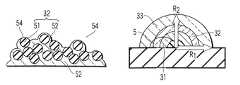
- FIG. 7Ashows the state of the trailing part (region A 1 ) in contact with the substrate 4
- FIG. 7Bshows the state of the top part (region B 1 ).
- the phosphor layer 32is constituted of the matrix (base matrix) 52 and the phosphor particles 51 dispersed in this matrix.
- the case of using a resin as the matrix 52is described.
- the second light transmissible layer 33is further formed on the phosphor layer 32 , as shown in FIG. 7A , a trailing 53 of the resin in the trailing part is reduced.
- the second light transmissible layer 33exists on the phosphor layer 32 , a distance between the phosphor particles 51 and air becomes larger. As a result, the effect of the total reflection at the phosphor particles-air boundary is small.
- the shape of the phosphor particles 51is never reflected on a surface. Since the second light transmissible layer 33 exists, smoothness of the surface of the multilayered structure is superior. By this, the total reflection is reduced, and it is possible to improve light extraction efficiency. Such a structure has been achieved by the inventors.
- FIG. 8A conventional structure is explained with reference to FIG. 8 , and FIGS. 9A , 9 B.
- the phosphor layer 32 formed on the light transmissible layer 31is in contact with air. Therefore, in the trailing part (A 2 ) of this phosphor layer 32 , as shown in FIG. 9A , the trailing 53 of the resin occurs largely. Such trailing leads to reduction of luminescence efficiency due to the total reflection/re-absorption increase.
- FIG. 9BOn the other hand, at the top part of the laminating structure as shown in FIG. 9B , unevenness reflecting the shape of the phosphor particles 51 occurs on the surface. The uppermost surface has unevenness by this and efficiency is reduced due to the total reflection/re-absorption increase.
- the first light transmissible layer 31can be formed using resin or a glass layer having light transmissibility.
- resinan arbitrary resin high in light transmissibility and strong in heat can be used.
- silicone resinepoxy resin, urea resin, fluororesin, acrylic resin, polyimide resin, or glass
- the epoxy resin or the silicone resinare the most suitable since they are easily available, easy to handle, and inexpensive.
- the shape of the outer periphery in the cross-section perpendicular to the substrate of the first light transmissible layer 31can be either one of semi-arc-shaped, parabolic-shaped, or U-shaped, or cornered shape having at least two straight lines. Thickness of the first light transmissible layer 31 is not especially limited as long as it is equal or more than large enough to completely cover the semiconductor light-emitting chip 2 .
- the width of the bottom surface including the semiconductor light-emitting chip 2 in contact with the substrate 4is from 200 to 500 ⁇ m. Furthermore, the height is within from 0.25 times to one time as much as the width of the bottom surface. As long as it is within this range, the light extraction efficiency from the semiconductor light-emitting chip 2 to outside (outside of device) of the phosphor layer 32 and the second light transmissible layer 33 can be improved sufficiently.
- the first light transmissible layer 31exists, the distance between the phosphor particles contained in the phosphor layer 32 and the semiconductor light-emitting chip 2 becomes larger. As a result, film thickness of the phosphor layer can be adjusted. Furthermore, by adjusting the phosphor layer to have the optimum thickness, it is possible to prevent re-absorption by the phosphor particles and to improve luminescence efficiency. In addition, since the first light transmissible layer 31 is formed between the phosphor layer 32 and the semiconductor light-emitting chip 2 , re-absorption is reduced.
- the phosphor layer 32can be formed by raw material prepared by adding a phosphor material (phosphor particles) into a matrix.
- a phosphor materialphosphor particles
- the matrixan arbitrary material high in both of light transmissibility and heat resistance can be used.
- silicone resin, epoxy resin, urea resin, fluororesin, acrylic resin, or polyimide resincan be used as the matrix.
- Epoxy resin or silicone resinare the most suitable especially since they are easily available, easy to handle and inexpensive.
- the matrixBesides the resins, glass, sintered material, ceramic structure combining YAG and Al 2 O 3 or the like can be used as the matrix.
- the same material as the above mentioned first light transmissible layer 31is preferably used.
- Refractive index of the matrixis the same as that of the first light transmissible layer 31 . It is desirable that the refractive index of the matrix is lower than that of the first light transmissible layer 31 and higher than that of the second light transmissible layer 33 .
- the shape of the outer periphery in the cross-section perpendicular to the substrate of the phosphor layer 32can be either one of semi-arc-shaped, parabolic-shaped, or U-shaped, or cornered shaped having at least two straight lines.
- the thickness of the phosphor layer 32is not limited as long as it is equal or more than large enough to completely cover the semiconductor light-emitting chip 2 and the first light transmissible layer 31 . It is desirable that the thickness of the phosphor layer 32 is within from 20 to 300 ⁇ m.
- the phosphor materialsare substance to absorb light within a region from ultraviolet to blue and to emit visible light.
- either one of the phosphor materialssuch as silicate based phosphor material, aluminate based phosphor material, nitride based phosphor material, sulfide based phosphor material, oxysulfide based phosphor material, YAG based phosphor material, phosphate borate based phosphor material, phosphate based phosphor material, and halophosphate based phosphor material can be used.
- At least a part of Sr, Ba or Camay be substituted by at least one selected from the group consisting of Mg, Be and Zn.
- silicate based phosphor material having other composition ratioMSiO 3 , MSiO 4 , M 2 SiO 3 , M 2 SiO 5 , and M 4 Si 2 O 8 (M is selected from the group consisting of Sr, Ba, Ca, Mg, Be, Zn, and Y) can be given.
- silicate based phosphor materialby substituting at least a part of Si by Ge, luminous color can be controlled. For instance, (Sr 1-x-y-z Ba x Ca y Eu z )2(Si 1-u Ge u )O 4 is given.
- At least one selected from Ti, Pb, Mn, As, Al, Pr, Tb, and Cemay be contained as an activator.
- Mis at least one selected from a group consisting of Ba, Sr, Mg, Zn, and Ca, and contains at least one of Eu and Mn as an activator.
- Mis at least one selected from a group consisting of Ba, Sr, Ca, Mg, Be, and Zn. Furthermore, at least one selected from the group consisting of Mn, Dy, Tb, and Nd. Ce may be contained as an activator.
- Nitride Based Phosphor Material(Mainly, Silicon Nitride Based Phosphor Material): L X Si Y N (2/3X+4/3Y) :Eu or L X Si Y O Z N (2/3X+4/3Y ⁇ 2/3Z) :Eu
- a phosphor materialat least one selected from the group consisting of Mg, Sr, Ca, Ba, Zn, B, Al, Cu, Mn, Cr, and Ni may be contained.
- at least one selected from the group consisting of Ce, Pr, Tb, Nd, and Lamay be contained as an activator.
- Xis a value satisfying 0 ⁇ x ⁇ 1.
- Mis at least one selected from the group consisting of Cu, Cl, Ag, Al, Fe, Cu, Ni, and Zn.
- Smay be substituted by at least one of Se and Te.
- Oxysulphide Phosphor Material(Ln 1-X Eu X )O 2 S
- Lnis at least one selected from the group consisting of Sc, Y, La, Gd, and Lu
- Xis a value satisfying 0 ⁇ X ⁇ 1.
- at least one selected from the group consisting of Tb, Pr, Mg, Ti, Nb, Ta, Ga, Sm, and Tmmay be contained as an activator.
- At least one of Cr and Tbmay be contained as an activator.
- MBO 3 :EuM is at least one selected from the group consisting of Y, La, Gd, Lu, and In.
- Tbmay be contained).
- Mis at least one selected from the group consisting of Mg, Ca, Sr, Ba, and Zn
- M′is at least one selected from the group consisting of Eu, Mn, Sn, Fe, and Cr.
- x, a, bis a value satisfying 0.001 ⁇ x ⁇ 0.5, 0 ⁇ a ⁇ 2, 0 ⁇ b ⁇ 3, and 0.3 ⁇ a+b.
- Timay be contained as an activator.
- Mis at least one selected from the group consisting of Ba, Sr, Ca, Mg, and Cd.
- xis a value satisfying 0 ⁇ x ⁇ 1. At least a part of C 1 may be substituted by F.
- At least one of Sb and Mnmay be contained as an activator.
- At least two kinds of the phosphor materialis blended and an inorganic phosphor material emitting light of a neutral color can be manufactured. For instance, by mixing coloring materials having colors corresponding respectively to RGB and manufacturing the matrix, the phosphor material enabling to obtain a white light can be obtained. Also in the case of mixing the phosphor material, the phosphor enabling to obtain the white light can be manufactured.
- the phosphor layer 32is adjusted so as not to transmit a light output from the semiconductor light-emitting chip 2 by adding the phosphor material in the matrix for a prescribed concentration.
- concentration of the phosphor material in the phosphor layer 32is preferred to be 20 wt % or more. For instance, 50 wt % or more of silicate based phosphor material is added into the matrix formed of a resin, and it is enabled to adjust not to transmit the light outputted from the semiconductor light-emitting chip 2 .
- the upper limit of concentration of the phosphor material in the phosphor layer 32becomes around 90 wt %.
- a desired effectcan be obtained. For instance, when using the phosphor particles having a diameter of 10 to 20 ⁇ m (average particle diameter 15 ⁇ m), since the homogeneous phosphor layer can be manufactured easily and thickness and shape of the layer are easily controllable. In the case of using phosphor particles having a diameter of 20 to 45 ⁇ m (average particle diameter 30 ⁇ m), light-emitting intensity and light-emitting are especially enhanced. In some cases, the phosphor particles having larger diameter can be used also.
- the second light transmissible layer 33can be formed of a resin or a glass layer having light transmissibility.
- a material having high in both of light transmissibility and heat resistancecan be used.
- silicone resin, epoxy resin, urea resin, fluororesin, acrylic resin, polyimide resin, or glasscan be given.
- the epoxy resin or the silicone resinis the most suitable for the second light transmissible layer 33 since they are easily available, easy to handle, and inexpensive.
- the second light transmissible layer 33can be formed by the same substance+ or a material having the same refractive index as that of the first light transmissible layer 31 or the matrix constituting the phosphor layer 32 . Otherwise, the second transmissible layer 33 may be formed by using a material having a lower refractive index than that of the first light transmissible layer 31 or the matrix constituting the phosphor layer 32 . In this case, the refractive index changes stepwise in the device, and a difference of the refractive index in the air-light transmissible layer 33 interface becomes smaller. As a result, the total reflection is reduced, and since light extraction efficiency is further improved, this becomes more preferable.
- the shape of the outer periphery in the cross-section of the second light transmissible layer 33can be either one semi-arc-shaped, palabola-shaped, or U-shaped, or cornered shaped having at least two straight lines.
- the thickness of the second light transmissible layer 33is 20 to 500 ⁇ m.
- the height of the multilayered structure covering the semiconductor light-emitting chip 2is from 0.25 times to one time as much as the width of the bottom surface. Within such a range, light extraction efficiency can be improved sufficiently.
- the shape of the outer periphery of the cross-section of the second light transmissible layer 33is semi-arc-shaped.
- the light extraction efficiencyhere means a reflective index and a transmission index of light from the semiconductor light-emitting chip in the air-resin interface.
- the second light transmissible layer 33 having the cross-section of the semi-arc-shaped outer peripherycan be formed by meeting the edge of the second light transmissible layer 33 with the outline of the substrate 4 as shown in FIG. 10A .
- the edge of the second light transmissible layer 33can be coincided with the outline of the substrate 4 . Firstly, the substrate is heated to the curing temperature of the resin, and applying the resin by a dispenser and solidifying the resin at nearly the same time, it can be molded in a semi-arc shape due to the surface tension.
- the edge of the second light transmissible layercan be coincided with the outline of the substrate also.
- the substrate 4 B having a convex part shown in FIG. 10B on the surfaceis used.
- the region of the phosphor layer 32becomes the convex part of a first step
- the region of the first light transmissible layer 31becomes the convex part of a second step.
- the substrate 4 C in which the groove is formed as shown in the FIG. 10Cmay be used.
- the groove of a cocentric circle centered in a semiconductor light-emitting chip mount partis installed on the surface of the substrate 4 c .
- the first light transmissible layer 31is formed in the region inside the groove, and the phosphor layer 32 is formed in the region of the groove. Furthermore, in that outside region, the second light transmissible layer 33 is formed.
- a surface treatmentis applied so as to become hydrophilic or hydrophobic.
- hydrophobic treatmentrepeling treatment by silicone
- the first light transmissible layer 31 and the phosphor layer 32are formed respectively in the regulated regions. As a result, the structure shown in FIG. 10A can be formed easily.
- the laminated structurecomprising the first light transmissible layer 31 , the phosphor layer 32 , and the second light transmissible layer 33 is formed inside the recess, efficiency is reduced by returning light from the side surface of this recess.
- thisis the case the cup shaped substrate is used. Since the inner peripheral face of the cup is a reflecting plate, returning light from this reflecting plate to the semiconductor light-emitting chip occurs, and efficiency is reduced.
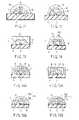
- the radius and the height of the laminated structureis shown respectively by R 1 and R 2 .
- the radius R 1is a distance from the center of the semiconductor light-emitting chip 2 to the outer periphery of the second light transmissible layer 33 on the surface of the substrate 4
- the height R 2is a distance from the plane surface for the semiconductor light-emitting chip of the substrate 4 to be mounted to the top of the second light transmissible layer 33 .
- R 1500 to 1,500 ⁇ m is most suitable. Furthermore, in the case of molding, there is no limit in the maximum value.
- the efficiencyis enhanced approximately to the degree exceeding 1.3 times as much as that before molding of R 1 within a range of 1/2 (R 1 ) ⁇ R 2 ⁇ 2R 1 . That is the case the respective layers have the height within a range from 0.25 to one times as much as the diameter of the bottom face. In the case of shifting out of this range, concretely, in the case of being longitudinally long or laterally long, the total reflection increases and the efficiency is reduced.
- the multilayered structure covering the semiconductor light-emitting chipcan be constituted in various shapes.
- the multilayered structurecan be formed by an arbitrary method depending on the shape.
- the multilayered structure of which the shape of the outer periphery in the cross-section is parabolicis shown.
- the multilayered structure of such a shapeis easy to be molded in a desired shape by controlling viscosity and temperature of the resin, and for instance, this can be manufactured by the following method. Firstly, the semiconductor light-emitting chip 2 is mounted onto the plane surface for the semiconductor light-emitting chip of the substrate 4 to be mounted. The first main electrode of the semiconductor light-emitting chip 2 and the wiring 42 of the substrate 4 are electrically connected and the second main electrode and the wiring 43 are electrically connected via the wire 5 . Afterwards a lighting test of the semiconductor light-emitting chip 2 is carried out.
- the resinis dripped to coat the surface of the substrate 4 in which the lighting confirmation has been carried out.
- the multilayered structureis manufactured by curing the resin.
- the viscosity of the resinBy adjusting the viscosity of the resin, surface tension of the resin, wettability of the substrate or temperature or the like, the outer peripheral shape in the cross section of the multilayered structure 3 can be made parabolic. In order to obtain such a shape, for instance, the viscosity of the resin can be made approximately at 2 to 10 Pa ⁇ s.
- the temperatureis made to be the ordinary temperature (25° C.) to 200° C. depending on the curing of the resin.
- the semiconductor light-emitting device having the multilayered structure 3 of which the shape of the cross-section is rectangularis shown.
- the multilayered structure 3 having this shapecan be manufactured easily, for instance, by molding the first light transmissible layer 31 , the phosphor layer 32 , and the second light transmissible layer 33 successively on the substrate 4 on which the semiconductor light-emitting chip 2 is mounted.
- the outer periphery on the cross-section perpendicular to the substrate plane surface of the multilayered structure in the semiconductor light-emitting device shown in FIG. 13includes three straight lines, and the space defined by such outer periphery and the surface of the substrate 4 becomes rectangular.
- the multilayered structure 3may be formed of which the cross-section perpendicular to the substrate plane surface is rectangular.
- the multilayered structure 3 shown in FIG. 13is manufactured by successively molding the resins to become raw materials of respective layers.
- the multilayered structure 3can be arranged on the plane surface for the semiconductor light-emitting chip of the substrate 4 to be mounted. Bonding can be carried out by arranging a resin adhesive having a similar composition to that of the first light transmissible layer 31 between the surface of the substrate 4 and the multilayered structure 3 .
- the second light transmissible layer 33can be formed in a different shape from the outer peripheral shape in the cross-section of the first light transmissible layer 31 .
- An example of a cross-section of the semiconductor light-emitting device including the first and the second light transmissible layers having such a shapeis shown in FIG. 14 .
- the cross-section perpendicular to the substrate plane surface of the first light transmissible layer 31is rectangular, and the shape of the outer periphery in the cross-section perpendicular to the substrate plane surface of the second light transmissible layer 33 is parabolic.
- the multilayered structure having such a shapecan be manufactured simply and easily by utilizing a tabular substance 32 a formed of ceramics containing the phosphor particles on the substrate 4 on which the semiconductor light-emitting chip 2 is mounted.
- the position of the tabular substance of the ceramics containing the phosphor particles worked in an appropriate sizeis fixed by the resin used in the first light transmissible layer 31 .
- the second light transmissible layer 33is formed by dripping the resin by the dispenser or the like.
- the substrate made of AINhas been prepared as the substrate 4 .
- This substrate 4can be manufactured easily by mold processing.
- the semiconductor light-emitting chip 2 having an InAlGaN light-emitting layer emitting a blue lighthas been mounted on the plane surface for the semiconductor light-emitting chip of the substrate 4 to be mounted.
- the size of the used semiconductor light-emitting chip 2is the bottom face of 300 ⁇ m square and a height of 120 ⁇ m.
- the first light transmissible layer 31was formed by the silicone resin on the substrate 4 while covering the semiconductor light-emitting chip 2 . While heating the substrate at 150° C., the resin was dripped using the dispenser and cured.
- the first light transmissible layer 31 of which the outer peripheral shape of the cross-section is parabolic and of which the thickness was 600 ⁇ mwas finally manufactured.
- the phosphor layer 32was formed.
- the silicone resinwas used as the matrix, and a raw material for phosphor layer was obtained by adding the yellow phosphor material (Sr, Ca, Ba) 2 SiO 4 :Eu having the average particle diameter of 30 ⁇ m at a concentration of 75 wt % to this matrix. While heating the substrate 4 at 150° C. in which the first light transmissible layer 31 has been formed, it was cured by dripping the f raw material using the dispenser. By this, the phosphor layer 32 of which the outer peripheral shape of the cross-section is parabolic and of which the thickness is 100 ⁇ m was manufactured.
- the second light transmissible layer 33was formed using the silicone resin. While heating the substrate having the first light transmissible layer 31 and the phosphor layer 32 at 150° C., the silicone resin is dripped by the dispenser and cured. By this, finally the second light transmissible layer 33 is formed of which the outer peripheral shape of the cross-section perpendicular to the substrate plane surface is parabolic and of which the thickness is 300 ⁇ m. By the above step, the semiconductor light-emitting device shown in FIG. 1 was obtained.
- the blue lightwas emitted. It was irradiated to the phosphor layer 32 from the semiconductor light-emitting chip 2 via the light transmissible layer 31 , absorbed a part of the blue light in the phosphor layer 32 and yellow light was emitted, and the semiconductor light-emitting device 1 emitted white light via the second light transmissible layer 33 .
- thisis a structure in which loss due to absorption of light inside the device is reduced. Since of this, exciting light emitted from the semiconductor light-emitting chip can be used effectively and light can be emitted at a high efficiency.
- the raw material for phosphor layercan be prepared by adding a yellow phosphor material (Sr, Ca, Ba) 2 SiO 4 :Eu having the average particle diameter of 50 ⁇ m to the silicone resin at the concentration of 75%.
- the semiconductor light-emitting devicecan be made in the same way as the above.
- An efficiency of the obtained semiconductor light-emitting deviceis expected to have approximately 10% improvement than the above described case.
- the average particle diameter of the phosphor particles used hereis 50 ⁇ m and it is larger than the above 30 ⁇ m. As the average particle diameter of the phosphor particles becomes larger, absorbance of the phosphor particles is improved and the number of the phosphor particles is decreased. For that reason, it is estimated that re-absorption by the phosphor particles reduced and luminescence efficiency was improved.
- the semiconductor light-emitting devicewas manufactured in a same constitution except that the first light transmissible layer 31 is not formed (comparative example 1).
- efficiency of the emitted lightis 80% of that in the case of the semiconductor light-emitting device of the example.
- the semiconductor light-emitting devicewas manufactured in a same constitution except that the second light transmissible layer 33 is not formed (comparative example 2).
- efficiency of the emitted lightwas 80% of that in the case of the semiconductor light-emitting device of the example.
- the semiconductor light-emitting devicewas manufactured in a same constitution except that the substrate 4 was changed to the cup, efficiency of the emitted light was 80% of that in the case of the semiconductor light-emitting device of the example (comparative example 3).
- efficiency of the emitted lightwas 80% of that in the case of the semiconductor light-emitting device of the embodiment.
- the semiconductor light-emitting device 1since this has a simple structure of the semiconductor light-emitting chip 2 and a plurality of thin layers made of resin, the number of parts is less, and it is possible to realize downsizing and high luminance.
- thicknesses of the first light transmissible layer 31 , the phosphor layer 32 and the second light transmissible layer 33were made 600, 100, and 300 ⁇ m respectively, it is not restricted to this. It can be changed appropriately depending on the size or the like of the semiconductor light-emitting chip 2 . For instance, in the case the size of the semiconductor light-emitting chip 2 is as large as 400 ⁇ m, the thicknesses of the first light transmissible layer 31 , the phosphor layer 32 , and the second light transmissible layer 33 can be changed to 800, 50, and 600 ⁇ m, respectively. In this case, there is an advantage that it can be manufactured easily at a high yield.
- the obtained luminescence efficiency of the semiconductor light-emitting deviceis further improved.
- the size of the semiconductor light-emitting chip 2is as small as 200 ⁇ m
- thicknesses of the first light transmissible layer 31 , the phosphor layer 32 , and the second light transmissible layer 33can be changed to 400, 100, and 100 ⁇ m. In this case, light-emitting luminance can be further improved.
- a third light transmissible layermay be further formed on the second light transmissible layer 33 .
- the cross-section of such a structureis shown in FIG. 15A and FIG. 15B .
- the first light transmissible layer 31 , the phosphor layer 32 , the second light transmissible layer 33 the third light transmissible layer 34 , and the fourth light transmissible layer 35are formed successively.
- the cross-section of such a multilayered structuremay be made rectangular.
- the refractive index of the third light transmissible layer 34is set to be lower than that of the second light transmissible layer 33 and that the refractive index of the fourth light transmissible layer 35 is set to be lower than the refractive index of the third light transmissible layer 34 .
- the refractive index of the third light transmissible layer 34can be set to be 1.42.
- the refractive index of the fourth light transmissible layer 35is desired to become around 1.2 to 1.4.
- the refractive indexes of the respective layerscan be adjusted, for instance, using a plurality of silicone resins having different substituting groups.
- the luminescence efficiencyis further improved than that in the case of a simple trilaminar structure comprising the first light transmissible layer 31 , the phosphor layer 32 , and the second light transmissible layer 33 .
- the phosphor layer of two layers or moremay be included. Since a plurality of the phosphor layers is present, light from the semiconductor light-emitting chip is absorbed more effectively, and luminescence efficiency can be improved.
- the cross-section view of those examplesis shown in FIG. 16A .
- the first light transmissible layer 31 , the phosphor layer 32 , and the second light transmissible layer 33are successively formed.
- the phosphor layer 32is constituted of a laminated layer of a red phosphor layer 32 R containing a red phosphor particles and a green phosphor layer 32 G containing a green phosphor particles.
- a blue light-emitting chip having an InGaN light-emitting layeris used as the semiconductor light-emitting chip 2 , and CaAlSiN 3 :Eu and (Sr, Ca, Ba) 2 SiO 4 :Eu can be used respectively as the red phosphor particles and the green phosphor particles.
- CaAlSiN 3 :Eu and (Sr, Ca, Ba) 2 SiO 4 :Eucan be used respectively as the red phosphor particles and the green phosphor particles.
- the phosphor layer 32can be constituted of the trilaminar structure of the red phosphor layer 32 R containing the red phosphor particles, the green phosphor layer 32 G containing the green phosphor particles, and the blue phosphor layer 32 B containing the blue phosphor particles.
- the obtained color reproducibility of the semiconductor light-emitting deviceis further improved.
- red, green and blueare successively laminated from the inside of the multilayered structure in the phosphor layer, re-absorption of light can be reduced more than the case of a structure in which a single phosphor layer is formed by mixing these three colors of phosphor particles. As a result, high luminescence efficiency can be obtained.
- the multilayered structure including the red phosphor layer, the green phosphor layer, and the blue phosphor layermay have a rectangular cross-section as shown in FIG. 17 .
- the semiconductor light-emitting shown in FIG. 17 devicewas fabricated.
- the semiconductor light-emitting chip 2As the semiconductor light-emitting chip 2 , a near-ultraviolet light-emitting LED chip having a light-emitting layer of GaN on the substrate 4 by a conventional method.
- the first light transmissible layer 31was formed by coating the silicone resin and curing. In doing this, the first light transmissible layer 31 was fabricated by solidifying it by a mold.
- the red phosphor layer 32 R including the red phosphor particles, the green phosphor layer 32 G including the green phosphor particles, and the blue phosphor layer 32 B including the blue phosphor particleswere successively formed, thereby obtaining the phosphor layer 32 .
- the red phosphor particles, the green phosphor particles, and the blue phosphor particlesLa 2 O 2 S:Eu, BaMg 2 Al 16 O 27 :Eu, Mn, and (Sr, Ca, Ba) 10 (PO 4 ) 6 Cl 2 :Eu were used, respectively.
- the filmed phosphor layerswere prepared, and these were laminated.
- the filmed phosphor layerBy using the filmed phosphor layer, a multilayered complicated shape can be fabricated easily.
- the deviceBy making the cross-section rectangular, the device can be fabricated more easily and manufactured inexpensively.
- the respective phosphor layersare set to be different in phosphor particles kinds or to have different concentrations.
- color renderingcan be improved.
- a structure in which the phosphor particles to emit light of a longer wavelengthis arranged in the inner layer is desirable.
- FIG. 18A and FIG. 18BOne of such examples is shown in FIG. 18A and FIG. 18B .
- the semiconductor light-emitting device shown in FIG. 18Aon the substrate 4 in which the semiconductor light-emitting chip 2 is installed, the first light transmissible layer 31 , the phosphor layer 32 , the second light transmissible layer 33 , the phosphor layer 32 , and the third light transmissible layer 34 are successively formed.
- two phosphor layers 32can contain the same kind of phosphor particles.
- the first light transmissible layer 31 , the red phosphor layer 32 R including the red phosphor particles, the second light transmissible layer 33 , the yellow phosphor layer 32 Y including the yellow phosphor particles, and the third light transmissible layer 34are successively formed.
- a semiconductor light-emitting deviceaccording to other embodiment furthermore is shown in FIG. 19 .
- a reflecting plate 6is installed at the outside of a second light transmissible layer 33 .
- the reflecting plate 6efficiently guides light emitted from the second light transmissible layer 33 into an arbitrary direction. As a result, the directivity of the light is enhanced, and color unevenness can be reduced still more.
- the reflecting plate 6can be formed of a material excellent in thermal conductivity. Especially, it is desired that heat generated by the action of the semiconductor light-emitting chip 2 , and for instance, Cu, AlN, Al 2 O 3 , BN, plastics, ceramics and diamond are notified. In order to enhance the reflectivity, reflecting coating of Ag or the like may be formed on the surface of the reflecting plate.
- the reflecting plate 6can be formed of another member (other parts) different from the substrate 4 and it can be fixed mechanically to the substrate 4 by an adhesive, tightening member or the like. Otherwise, the reflecting plate 6 may be constituted by integrated molding with the substrate 4 .
- a multiple chip module structure as shown in FIG. 20may be adopted.
- FIG. 20A plan view of such a semiconductor light-emitting device 1 is shown in FIG. 21 .
- the number of the semiconductor light-emitting chip 2can be changed appropriately and arranged in an arbitrary shape. For instance as shown in FIG. 22 , four semiconductor light-emitting chips 2 may be arranged in a straight line. On respective light-emitting chip, the first light transmissible layer 31 and the phosphor layer are successively formed. The second light transmissible layer 33 is formed covering the four phosphor layers 32 collectively. Otherwise, as shown in FIG. 23 , individual semiconductor light-emitting chips can be covered only by the first light transmissible layer 31 . The phosphor layer 32 and the second light transmissible layer 33 collectively cover four first light transmissible layers 31 .
- the semiconductor light-emitting devicesince the semiconductor light-emitting chip mounted on the substrate is covered by a multilayered structure including the first light transmissible layer, the phosphor layer, and the second light transmissible layer, a highly efficient output of light with high luminance has been enabled.
- Usage of the semiconductor light-emitting device according to the embodimentis not limited only to the above described examples, but can be applied to various applications. For instance, it can be applied to general illumination appliances, office use illumination fixtures, or back lights for liquid crystal display devices of televisions or personal computers, and in addition, to lighting fixtures for automobiles, motorcycles, or bicycles or the like. In respective cases, light with high luminance can be outputted at a high output.
- a semiconductor light-emitting devicein which light of high luminance can be outputted at a high efficiency.
Landscapes
- Led Device Packages (AREA)
- Led Devices (AREA)
Abstract
Description
Claims (12)
Applications Claiming Priority (2)
| Application Number | Priority Date | Filing Date | Title |
|---|---|---|---|
| JP2006094875AJP2007273562A (en) | 2006-03-30 | 2006-03-30 | Semiconductor light emitting device |
| JP2006-094875 | 2006-03-30 |
Publications (2)
| Publication Number | Publication Date |
|---|---|
| US20070228390A1 US20070228390A1 (en) | 2007-10-04 |
| US8294165B2true US8294165B2 (en) | 2012-10-23 |
Family
ID=38557492
Family Applications (1)
| Application Number | Title | Priority Date | Filing Date |
|---|---|---|---|
| US11/668,218Active2028-08-02US8294165B2 (en) | 2006-03-30 | 2007-01-29 | Semiconductor light-emitting device |
Country Status (3)
| Country | Link |
|---|---|
| US (1) | US8294165B2 (en) |
| JP (1) | JP2007273562A (en) |
| KR (1) | KR100983428B1 (en) |
Cited By (16)
| Publication number | Priority date | Publication date | Assignee | Title |
|---|---|---|---|---|
| US20110031891A1 (en)* | 2005-06-28 | 2011-02-10 | Seoul Opto Device Co., Ltd. | Light emitting device for ac power operation |
| US20110163322A1 (en)* | 2009-08-10 | 2011-07-07 | Jae Soo Yoo | Phosphor, phosphor manufacturing method, and white light emitting device |
| US20110193118A1 (en)* | 2010-02-09 | 2011-08-11 | Oshima Yukitoyo | Light emitting device and manufacturing method thereof |
| US20120037882A1 (en)* | 2010-08-10 | 2012-02-16 | Jae Soo Yoo | Phosphor, phosphor manufacturing method, and white light emitting device |
| US8670087B2 (en) | 2008-11-18 | 2014-03-11 | Lg Innotek Co., Ltd. | Light emitting module and display device having the same |
| US20140210628A1 (en)* | 2011-08-22 | 2014-07-31 | Electronics And Telecommunications Research Institute | Metal-insulator transition (mit) device molded by clear compound epoxy and fire detecting device including the mit device |
| US20140268762A1 (en)* | 2013-03-15 | 2014-09-18 | Cree, Inc. | Multi-Layer Polymeric Lens and Unitary Optic Member for LED Light Fixtures and Method of Manufacture |
| US8896216B2 (en) | 2005-06-28 | 2014-11-25 | Seoul Viosys Co., Ltd. | Illumination system |
| US20150034987A1 (en)* | 2013-07-30 | 2015-02-05 | Nichia Corporation | Light emitting device and method for manufacturing light emitting device |
| US9909058B2 (en) | 2009-09-02 | 2018-03-06 | Lg Innotek Co., Ltd. | Phosphor, phosphor manufacturing method, and white light emitting device |
| US10347800B2 (en) | 2012-05-14 | 2019-07-09 | Lumileds Llc | Light emitting device with nanostructured phosphor |
| US10422503B2 (en) | 2009-10-30 | 2019-09-24 | Ideal Industries Lighting Llc | One-piece multi-lens optical member and method of manufacture |
| US10559727B2 (en) | 2017-07-25 | 2020-02-11 | Shenzhen China Star Optoelectronics Semiconductor Display Technology Co., Ltd. | Manufacturing method of colorful Micro-LED, display modlue and terminals |
| US11211524B2 (en)* | 2017-08-01 | 2021-12-28 | Osram Oled Gmbh | Method of producing an optoelectronic component |
| US11598491B2 (en) | 2011-02-22 | 2023-03-07 | Quarkstar Llc | Solid state lamp using light emitting strips |
| US11906846B2 (en) | 2020-09-16 | 2024-02-20 | Samsung Electronics Co., Ltd. | Display device and manufacturing method therefor |
Families Citing this family (88)
| Publication number | Priority date | Publication date | Assignee | Title |
|---|---|---|---|---|
| US9929326B2 (en) | 2004-10-29 | 2018-03-27 | Ledengin, Inc. | LED package having mushroom-shaped lens with volume diffuser |
| US8816369B2 (en) | 2004-10-29 | 2014-08-26 | Led Engin, Inc. | LED packages with mushroom shaped lenses and methods of manufacturing LED light-emitting devices |
| US8324641B2 (en)* | 2007-06-29 | 2012-12-04 | Ledengin, Inc. | Matrix material including an embedded dispersion of beads for a light-emitting device |
| US8134292B2 (en)* | 2004-10-29 | 2012-03-13 | Ledengin, Inc. | Light emitting device with a thermal insulating and refractive index matching material |
| JP4557824B2 (en)* | 2005-07-04 | 2010-10-06 | 株式会社東芝 | Light emitting device and manufacturing method thereof |
| JP2008153466A (en)* | 2006-12-18 | 2008-07-03 | Matsushita Electric Works Ltd | Light-emitting device |
| JP5207511B2 (en)* | 2007-05-23 | 2013-06-12 | 独立行政法人産業技術総合研究所 | Semiconductor element |
| US20080308819A1 (en)* | 2007-06-15 | 2008-12-18 | Tpo Displays Corp. | Light-Emitting Diode Arrays and Methods of Manufacture |
| TWI365546B (en)* | 2007-06-29 | 2012-06-01 | Ind Tech Res Inst | Light emitting diode device and fabrication method thereof |
| JP5044329B2 (en)* | 2007-08-31 | 2012-10-10 | 株式会社東芝 | Light emitting device |
| JP5193586B2 (en)* | 2007-12-25 | 2013-05-08 | 株式会社東芝 | Semiconductor light emitting device |
| WO2009107535A1 (en)* | 2008-02-25 | 2009-09-03 | 株式会社東芝 | White led lamp, backlight, light emitting device, display device and lighting device |
| JP5216384B2 (en)* | 2008-03-19 | 2013-06-19 | 株式会社東芝 | Light emitting device |
| TW201007091A (en)* | 2008-05-08 | 2010-02-16 | Lok F Gmbh | Lamp device |
| JP5512515B2 (en)* | 2008-05-30 | 2014-06-04 | シャープ株式会社 | Light emitting device, surface light source, and liquid crystal display device |
| US8159131B2 (en)* | 2008-06-30 | 2012-04-17 | Bridgelux, Inc. | Light emitting device having a transparent thermally conductive layer |
| US8680550B2 (en)* | 2008-07-03 | 2014-03-25 | Samsung Electronics Co., Ltd. | Wavelength-converting light emitting diode (LED) chip and LED device equipped with chip |
| DE102008035255B4 (en)* | 2008-07-29 | 2021-10-07 | OSRAM Opto Semiconductors Gesellschaft mit beschränkter Haftung | Optoelectronic semiconductor component and method for producing an optoelectronic semiconductor component |
| JP4881358B2 (en) | 2008-08-28 | 2012-02-22 | 株式会社東芝 | Light emitting device |
| JP5571889B2 (en)* | 2008-08-29 | 2014-08-13 | 株式会社東芝 | Light emitting device and lighting device |
| KR101008442B1 (en)* | 2008-09-29 | 2011-01-14 | 한국광기술원 | Light emitting diode package and its manufacturing method |
| US8075165B2 (en)* | 2008-10-14 | 2011-12-13 | Ledengin, Inc. | Total internal reflection lens and mechanical retention and locating device |
| US20100109025A1 (en)* | 2008-11-05 | 2010-05-06 | Koninklijke Philips Electronics N.V. | Over the mold phosphor lens for an led |
| US8507300B2 (en)* | 2008-12-24 | 2013-08-13 | Ledengin, Inc. | Light-emitting diode with light-conversion layer |
| US20100244064A1 (en)* | 2009-03-27 | 2010-09-30 | Avago Technologies Ecbu Ip (Singapore) Pte. Ltd. | Light source |
| JP5423120B2 (en)* | 2009-04-17 | 2014-02-19 | 三菱化学株式会社 | Semiconductor light emitting device |
| JP5444919B2 (en)* | 2009-07-29 | 2014-03-19 | ソニー株式会社 | Illumination device and liquid crystal display device |
| US20110031516A1 (en)* | 2009-08-07 | 2011-02-10 | Koninklijke Philips Electronics N.V. | Led with silicone layer and laminated remote phosphor layer |
| JP2011060884A (en)* | 2009-09-08 | 2011-03-24 | Sharp Corp | Semiconductor light-emitting device and lighting fixture for vehicle |
| JP5379615B2 (en) | 2009-09-09 | 2013-12-25 | パナソニック株式会社 | Lighting device |
| JP2011077481A (en)* | 2009-10-02 | 2011-04-14 | Sanyu Rec Co Ltd | Method of manufacturing led device |
| JP5113820B2 (en)* | 2009-10-27 | 2013-01-09 | パナソニック株式会社 | Light emitting device |
| JP5473553B2 (en)* | 2009-11-18 | 2014-04-16 | 京セラ株式会社 | Optical module and droplet curing device |
| KR100986380B1 (en) | 2009-11-20 | 2010-10-08 | 엘지이노텍 주식회사 | Light emitting apparatus |
| JP5050045B2 (en) | 2009-12-22 | 2012-10-17 | 株式会社東芝 | Light emitting device |
| JP5047264B2 (en)* | 2009-12-22 | 2012-10-10 | 株式会社東芝 | Light emitting device |
| KR20110087579A (en)* | 2010-01-26 | 2011-08-03 | 삼성엘이디 주식회사 | LED module and backlight unit having the same |
| US9039216B2 (en)* | 2010-04-01 | 2015-05-26 | Lg Innotek Co., Ltd. | Light emitting device package and light unit having the same |
| JP5451534B2 (en)* | 2010-06-07 | 2014-03-26 | 株式会社東芝 | Semiconductor light emitting device and method for manufacturing semiconductor light emitting device |
| JP5426484B2 (en) | 2010-06-07 | 2014-02-26 | 株式会社東芝 | Manufacturing method of semiconductor light emitting device |
| US8450929B2 (en) | 2010-06-28 | 2013-05-28 | Panasonic Corporation | Light emitting device, backlight unit, liquid crystal display apparatus, and lighting apparatus |
| US20120043569A1 (en)* | 2010-08-23 | 2012-02-23 | Kabushiki Kaisha Toshiba | Light emitting device and manufacturing method thereof |
| JP5076017B2 (en)* | 2010-08-23 | 2012-11-21 | 株式会社東芝 | Light emitting device |
| JP5172915B2 (en) | 2010-09-07 | 2013-03-27 | 株式会社東芝 | Light emitting device |
| US8436527B2 (en)* | 2010-09-07 | 2013-05-07 | Kabushiki Kaisha Toshiba | Light emitting device |
| JP5675248B2 (en)* | 2010-09-29 | 2015-02-25 | スタンレー電気株式会社 | Light source device and lighting device |
| US8891051B2 (en)* | 2010-10-25 | 2014-11-18 | Semiconductor Energy Laboratory Co., Ltd. | Backlight and display device |
| JP5877992B2 (en) | 2010-10-25 | 2016-03-08 | 株式会社半導体エネルギー研究所 | Display device |
| JP5320374B2 (en)* | 2010-11-09 | 2013-10-23 | 株式会社東芝 | Method for manufacturing light emitting device |
| DE102010061801A1 (en)* | 2010-11-23 | 2012-05-24 | Tridonic Jennersdorf Gmbh | LED module with common color conversion module for at least two LED chips |
| WO2012081247A1 (en)* | 2010-12-17 | 2012-06-21 | パナソニック株式会社 | Led device and method for manufacturing same |
| EP2472578B1 (en)* | 2010-12-28 | 2020-06-03 | Nichia Corporation | Light emitting device |
| TWI441361B (en)* | 2010-12-31 | 2014-06-11 | Interlight Optotech Corp | Light-emitting diode package structure and manufacturing method thereof |
| US8953120B2 (en) | 2011-01-07 | 2015-02-10 | Semiconductor Energy Laboratory Co., Ltd. | Display device |
| KR101210066B1 (en) | 2011-01-31 | 2012-12-07 | 엘지이노텍 주식회사 | Light conversion member and display device having the same |
| CN102252273A (en)* | 2011-04-12 | 2011-11-23 | 广东佛照新光源科技有限公司 | Wavelength conversion device and manufacturing method thereof |
| JP5899507B2 (en)* | 2011-04-27 | 2016-04-06 | パナソニックIpマネジメント株式会社 | LIGHT EMITTING DEVICE AND LIGHTING DEVICE USING THE SAME |
| JP2012248553A (en)* | 2011-05-25 | 2012-12-13 | Panasonic Corp | Light-emitting device and luminaire using the same |
| JP5862066B2 (en)* | 2011-06-16 | 2016-02-16 | 東レ株式会社 | Phosphor-containing sheet, LED light-emitting device using the same, and manufacturing method thereof |
| KR101305696B1 (en) | 2011-07-14 | 2013-09-09 | 엘지이노텍 주식회사 | Display device and optical member |
| KR20130009020A (en) | 2011-07-14 | 2013-01-23 | 엘지이노텍 주식회사 | Optical member, display device having the same and method of fabricating the same |
| KR101893494B1 (en) | 2011-07-18 | 2018-08-30 | 엘지이노텍 주식회사 | Optical member and display device having the same |
| KR101262520B1 (en) | 2011-07-18 | 2013-05-08 | 엘지이노텍 주식회사 | Optical member and display device including same |
| KR101241549B1 (en) | 2011-07-18 | 2013-03-11 | 엘지이노텍 주식회사 | Optical member, display device having the same and method of fabricating the same |
| KR101294415B1 (en)* | 2011-07-20 | 2013-08-08 | 엘지이노텍 주식회사 | Optical member and display device having the same |
| JP5988073B2 (en)* | 2011-11-01 | 2016-09-07 | 東芝ライテック株式会社 | Light emitting module and lighting device |
| KR101251815B1 (en) | 2011-11-07 | 2013-04-09 | 엘지이노텍 주식회사 | Optical sheet and display device having the same |
| JPWO2013105514A1 (en)* | 2012-01-13 | 2015-05-11 | コニカミノルタ株式会社 | LED device |
| WO2013121903A1 (en)* | 2012-02-13 | 2013-08-22 | コニカミノルタ株式会社 | Wavelength conversion element and method for manufacturing same, and light-emitting device and method for manufacturing same |
| US9897284B2 (en) | 2012-03-28 | 2018-02-20 | Ledengin, Inc. | LED-based MR16 replacement lamp |
| KR20130124632A (en)* | 2012-05-07 | 2013-11-15 | 주식회사 포스코엘이디 | Led illuminating apparatus and method for fabricating wavelength conversion member used for the apparatus |
| JP6325536B2 (en)* | 2012-07-05 | 2018-05-16 | コーニンクレッカ フィリップス エヌ ヴェKoninklijke Philips N.V. | Phosphor separated from LED by transparent spacer |
| TW201403875A (en)* | 2012-07-13 | 2014-01-16 | Ritedia Corp | White light emitting diode |
| DE102012112307A1 (en)* | 2012-12-14 | 2014-06-18 | Osram Opto Semiconductors Gmbh | Optoelectronic semiconductor component and method for producing an optoelectronic semiconductor component |
| KR102059032B1 (en)* | 2013-01-07 | 2020-02-11 | 엘지이노텍 주식회사 | A light emitting device package |
| CN104853587A (en)* | 2013-02-15 | 2015-08-19 | 夏普株式会社 | LED light source for plant cultivation |
| JP6244130B2 (en)* | 2013-07-26 | 2017-12-06 | 新光電気工業株式会社 | Light emitting element mounting package and light emitting element package |
| JP6244857B2 (en)* | 2013-11-26 | 2017-12-13 | 日亜化学工業株式会社 | Light emitting device |
| TW201526301A (en)* | 2013-12-30 | 2015-07-01 | Cheng Wen | Invisible light emitting device |
| JP6432416B2 (en)* | 2014-04-14 | 2018-12-05 | 日亜化学工業株式会社 | Semiconductor device |
| EP3147956B1 (en)* | 2015-09-22 | 2023-05-03 | Samsung Electronics Co., Ltd. | Led package, backlight unit and illumination device including same, and liquid crystal display device |
| WO2017111752A1 (en)* | 2015-12-22 | 2017-06-29 | Ozyegin Universitesi | Lighting interlayers for optical paths of light emitting or absorbing systems |
| JP7108171B2 (en)* | 2016-12-27 | 2022-07-28 | 日亜化学工業株式会社 | light emitting device |
| JP2018195778A (en)* | 2017-05-22 | 2018-12-06 | シチズン電子株式会社 | Light emitting device |
| CN107437531A (en)* | 2017-07-25 | 2017-12-05 | 深圳市华星光电半导体显示技术有限公司 | Make color M icro LED method, display module and terminal |
| JP7481610B2 (en)* | 2019-12-26 | 2024-05-13 | 日亜化学工業株式会社 | Light-emitting device |
| WO2022044709A1 (en)* | 2020-08-31 | 2022-03-03 | 京セラ株式会社 | Display device and production method for display device |
| JP7389363B2 (en)* | 2021-05-26 | 2023-11-30 | 日亜化学工業株式会社 | light emitting device |
Citations (55)
| Publication number | Priority date | Publication date | Assignee | Title |
|---|---|---|---|---|
| JPS5079379A (en) | 1973-11-13 | 1975-06-27 | ||
| JPH0799345A (en) | 1993-09-28 | 1995-04-11 | Nichia Chem Ind Ltd | Light emitting diode |
| JPH1056208A (en) | 1997-05-17 | 1998-02-24 | Nichia Chem Ind Ltd | Light emitting diode manufacturing method |
| JPH10173241A (en) | 1996-12-12 | 1998-06-26 | Sharp Corp | Chip component type LED and method of manufacturing the same |
| JPH1187778A (en) | 1997-09-02 | 1999-03-30 | Toshiba Corp | Semiconductor light emitting element, semiconductor light emitting device and method for manufacturing the same |
| JPH11163397A (en) | 1997-11-25 | 1999-06-18 | Matsushita Electric Works Ltd | Led element and its manufacture |
| JPH11214752A (en) | 1998-01-21 | 1999-08-06 | Matsushita Electron Corp | Semiconductor light-emitting device |
| US5962971A (en) | 1997-08-29 | 1999-10-05 | Chen; Hsing | LED structure with ultraviolet-light emission chip and multilayered resins to generate various colored lights |
| JP2000031531A (en) | 1998-07-14 | 2000-01-28 | Toshiba Electronic Engineering Corp | Light emitting device |
| JP2001044514A (en) | 1993-09-28 | 2001-02-16 | Nichia Chem Ind Ltd | Light emitting diode |
| JP2001203392A (en) | 2000-01-19 | 2001-07-27 | Matsushita Electric Works Ltd | Light emitting diode |
| JP2002042525A (en) | 2000-07-26 | 2002-02-08 | Toyoda Gosei Co Ltd | Planar light source |
| JP2002118293A (en) | 2000-07-31 | 2002-04-19 | Nichia Chem Ind Ltd | Light-emitting device and forming method thereof |
| JP2002241586A (en) | 2001-02-19 | 2002-08-28 | Matsushita Electric Ind Co Ltd | Wavelength conversion paste material, composite light-emitting element, semiconductor light-emitting device, and method for manufacturing the same |
| JP2002359404A (en) | 2001-05-31 | 2002-12-13 | Nichia Chem Ind Ltd | Light emitting device using phosphor |
| US20030132701A1 (en)* | 2001-11-01 | 2003-07-17 | Nichia Corporation | Light emitting apparatus provided with fluorescent substance and semiconductor light emitting device, and method of manufacturing the same |
| JP2003224306A (en) | 2002-01-21 | 2003-08-08 | Solidlite Corp | Method for manufacturing white light emitting diode |
| US6657382B2 (en)* | 2000-07-21 | 2003-12-02 | Nichia Corporation | Light emitting device, display apparatus with an array of light emitting devices, and display apparatus method of manufacture |
| JP2004006227A (en) | 2002-04-10 | 2004-01-08 | Nichia Chem Ind Ltd | Illumination device and control method thereof |
| JP2004048040A (en) | 2003-08-26 | 2004-02-12 | Toshiba Electronic Engineering Corp | Semiconductor light emitting device |
| JP2004080058A (en) | 2003-11-25 | 2004-03-11 | Nichia Chem Ind Ltd | Light emitting diode |
| JP2004087812A (en) | 2002-08-27 | 2004-03-18 | Sanyo Electric Co Ltd | Light emitting device |
| JP2004111882A (en) | 2002-09-20 | 2004-04-08 | Toyoda Gosei Co Ltd | Light emitting device |
| US6734465B1 (en)* | 2001-11-19 | 2004-05-11 | Nanocrystals Technology Lp | Nanocrystalline based phosphors and photonic structures for solid state lighting |
| JP2004266148A (en) | 2003-03-03 | 2004-09-24 | Toyoda Gosei Co Ltd | Light emitting device and manufacturing method thereof |
| JP2004273798A (en) | 2003-03-10 | 2004-09-30 | Toyoda Gosei Co Ltd | Light emitting device |
| US20040227149A1 (en)* | 2003-04-30 | 2004-11-18 | Cree, Inc. | High powered light emitter packages with compact optics |
| US20040256706A1 (en)* | 2003-06-20 | 2004-12-23 | Shintaro Nakashima | Molded package and semiconductor device using molded package |
| US20050057144A1 (en)* | 2003-09-17 | 2005-03-17 | Yasumasa Morita | Semiconductor light-emitting device |
| US6898014B2 (en)* | 2002-08-30 | 2005-05-24 | Ricoh Company, Ltd. | Micro lens molding piece, micro lens molding piece producing method, micro lens stamper, micro lens stamper producing method, micro lens mold member, plastic lens array sheet, and projector |
| US20050133808A1 (en)* | 2003-09-11 | 2005-06-23 | Kyocera Corporation | Package for housing light-emitting element, light-emitting apparatus and illumination apparatus |
| JP2005197509A (en) | 2003-01-10 | 2005-07-21 | Toyoda Gosei Co Ltd | Light emitting device |
| JP2005232311A (en) | 2004-02-19 | 2005-09-02 | Nichia Chem Ind Ltd | Alkaline earth metal borate phosphor and light emitting device using the same |
| US20050211991A1 (en)* | 2004-03-26 | 2005-09-29 | Kyocera Corporation | Light-emitting apparatus and illuminating apparatus |
| JP2005276976A (en) | 2004-03-24 | 2005-10-06 | Matsushita Electric Ind Co Ltd | LED light source and LED lighting device |
| JP2005277127A (en) | 2004-03-25 | 2005-10-06 | Stanley Electric Co Ltd | Light emitting device |
| JP2005276883A (en) | 2004-03-23 | 2005-10-06 | Mitsubishi Electric Corp | White LED light source |
| JP2005272484A (en) | 2004-03-22 | 2005-10-06 | Fujikura Ltd | Light emitting device |
| US6960878B2 (en)* | 2001-01-24 | 2005-11-01 | Nichia Corporation | Light emitting diode, optical semiconductor element and epoxy resin composition suitable for optical semiconductor element and production methods therefor |
| JP2005332963A (en) | 2004-05-19 | 2005-12-02 | Shoei Chem Ind Co | Light emitting device |
| JP2006013347A (en) | 2004-06-29 | 2006-01-12 | Stanley Electric Co Ltd | Sealing resin for light emitting diode and light emitting diode using the same |
| JP2006032726A (en) | 2004-07-16 | 2006-02-02 | Kyocera Corp | Light emitting device |
| US20060055309A1 (en)* | 2004-09-14 | 2006-03-16 | Masato Ono | Light emitting device |
| US7019335B2 (en)* | 2001-04-17 | 2006-03-28 | Nichia Corporation | Light-emitting apparatus |
| US20060081814A1 (en) | 2004-10-18 | 2006-04-20 | Kabushiki Kaisha Toshiba | Fluorescent substance and light-emitting device using the same |
| US20060255353A1 (en)* | 2003-09-08 | 2006-11-16 | Taskar Nikhil R | Light efficient packaging configurations for LED lamps using high refractive index encapsulants |
| US20060255716A1 (en)* | 2005-05-16 | 2006-11-16 | Koito Manufacturing Co., Ltd. | Light emitting apparatus and vehicle lamp |
| US20070001568A1 (en)* | 2005-07-04 | 2007-01-04 | Kei Kaneko | Light-emitting device |
| US20070013304A1 (en)* | 2005-07-15 | 2007-01-18 | Kei Kaneko | Light-emitting device |
| US7352011B2 (en)* | 2004-11-15 | 2008-04-01 | Philips Lumileds Lighting Company, Llc | Wide emitting lens for LED useful for backlighting |
| US7354785B2 (en)* | 2002-06-28 | 2008-04-08 | Kabay & Company Pty Ltd. | Electroluminescent light emitting device |
| US7388232B2 (en)* | 2003-10-31 | 2008-06-17 | Toyoda Gosei Co., Ltd. | Light emitting element and light emitting device |
| US7635873B2 (en)* | 2004-03-31 | 2009-12-22 | Stanley Electric Co., Ltd. | Semiconductor light emitting device and method of manufacturing the same |
| US7868343B2 (en)* | 2004-04-06 | 2011-01-11 | Cree, Inc. | Light-emitting devices having multiple encapsulation layers with at least one of the encapsulation layers including nanoparticles and methods of forming the same |
| US7939843B2 (en)* | 2006-10-26 | 2011-05-10 | Toyoda Gosei Co., Ltd. | Light emitting device and high refractive index layer |
Family Cites Families (1)
| Publication number | Priority date | Publication date | Assignee | Title |
|---|---|---|---|---|
| KR101114305B1 (en) | 2004-12-24 | 2012-03-08 | 쿄세라 코포레이션 | Light-emitting device and illuminating device |
- 2006
- 2006-03-30JPJP2006094875Apatent/JP2007273562A/enactivePending
- 2007
- 2007-01-29USUS11/668,218patent/US8294165B2/enactiveActive
- 2007-03-29KRKR1020070030695Apatent/KR100983428B1/ennot_activeExpired - Fee Related
Patent Citations (55)
| Publication number | Priority date | Publication date | Assignee | Title |
|---|---|---|---|---|
| JPS5079379A (en) | 1973-11-13 | 1975-06-27 | ||
| JPH0799345A (en) | 1993-09-28 | 1995-04-11 | Nichia Chem Ind Ltd | Light emitting diode |
| JP2001044514A (en) | 1993-09-28 | 2001-02-16 | Nichia Chem Ind Ltd | Light emitting diode |
| JPH10173241A (en) | 1996-12-12 | 1998-06-26 | Sharp Corp | Chip component type LED and method of manufacturing the same |
| JPH1056208A (en) | 1997-05-17 | 1998-02-24 | Nichia Chem Ind Ltd | Light emitting diode manufacturing method |
| US5962971A (en) | 1997-08-29 | 1999-10-05 | Chen; Hsing | LED structure with ultraviolet-light emission chip and multilayered resins to generate various colored lights |
| JPH1187778A (en) | 1997-09-02 | 1999-03-30 | Toshiba Corp | Semiconductor light emitting element, semiconductor light emitting device and method for manufacturing the same |
| JPH11163397A (en) | 1997-11-25 | 1999-06-18 | Matsushita Electric Works Ltd | Led element and its manufacture |
| JPH11214752A (en) | 1998-01-21 | 1999-08-06 | Matsushita Electron Corp | Semiconductor light-emitting device |
| JP2000031531A (en) | 1998-07-14 | 2000-01-28 | Toshiba Electronic Engineering Corp | Light emitting device |
| JP2001203392A (en) | 2000-01-19 | 2001-07-27 | Matsushita Electric Works Ltd | Light emitting diode |
| US6657382B2 (en)* | 2000-07-21 | 2003-12-02 | Nichia Corporation | Light emitting device, display apparatus with an array of light emitting devices, and display apparatus method of manufacture |
| JP2002042525A (en) | 2000-07-26 | 2002-02-08 | Toyoda Gosei Co Ltd | Planar light source |
| JP2002118293A (en) | 2000-07-31 | 2002-04-19 | Nichia Chem Ind Ltd | Light-emitting device and forming method thereof |
| US6960878B2 (en)* | 2001-01-24 | 2005-11-01 | Nichia Corporation | Light emitting diode, optical semiconductor element and epoxy resin composition suitable for optical semiconductor element and production methods therefor |
| JP2002241586A (en) | 2001-02-19 | 2002-08-28 | Matsushita Electric Ind Co Ltd | Wavelength conversion paste material, composite light-emitting element, semiconductor light-emitting device, and method for manufacturing the same |
| US7019335B2 (en)* | 2001-04-17 | 2006-03-28 | Nichia Corporation | Light-emitting apparatus |
| JP2002359404A (en) | 2001-05-31 | 2002-12-13 | Nichia Chem Ind Ltd | Light emitting device using phosphor |
| US20030132701A1 (en)* | 2001-11-01 | 2003-07-17 | Nichia Corporation | Light emitting apparatus provided with fluorescent substance and semiconductor light emitting device, and method of manufacturing the same |
| US6734465B1 (en)* | 2001-11-19 | 2004-05-11 | Nanocrystals Technology Lp | Nanocrystalline based phosphors and photonic structures for solid state lighting |
| JP2003224306A (en) | 2002-01-21 | 2003-08-08 | Solidlite Corp | Method for manufacturing white light emitting diode |
| JP2004006227A (en) | 2002-04-10 | 2004-01-08 | Nichia Chem Ind Ltd | Illumination device and control method thereof |
| US7354785B2 (en)* | 2002-06-28 | 2008-04-08 | Kabay & Company Pty Ltd. | Electroluminescent light emitting device |
| JP2004087812A (en) | 2002-08-27 | 2004-03-18 | Sanyo Electric Co Ltd | Light emitting device |
| US6898014B2 (en)* | 2002-08-30 | 2005-05-24 | Ricoh Company, Ltd. | Micro lens molding piece, micro lens molding piece producing method, micro lens stamper, micro lens stamper producing method, micro lens mold member, plastic lens array sheet, and projector |
| JP2004111882A (en) | 2002-09-20 | 2004-04-08 | Toyoda Gosei Co Ltd | Light emitting device |
| JP2005197509A (en) | 2003-01-10 | 2005-07-21 | Toyoda Gosei Co Ltd | Light emitting device |
| JP2004266148A (en) | 2003-03-03 | 2004-09-24 | Toyoda Gosei Co Ltd | Light emitting device and manufacturing method thereof |
| JP2004273798A (en) | 2003-03-10 | 2004-09-30 | Toyoda Gosei Co Ltd | Light emitting device |
| US20040227149A1 (en)* | 2003-04-30 | 2004-11-18 | Cree, Inc. | High powered light emitter packages with compact optics |
| US20040256706A1 (en)* | 2003-06-20 | 2004-12-23 | Shintaro Nakashima | Molded package and semiconductor device using molded package |
| JP2004048040A (en) | 2003-08-26 | 2004-02-12 | Toshiba Electronic Engineering Corp | Semiconductor light emitting device |
| US20060255353A1 (en)* | 2003-09-08 | 2006-11-16 | Taskar Nikhil R | Light efficient packaging configurations for LED lamps using high refractive index encapsulants |
| US20050133808A1 (en)* | 2003-09-11 | 2005-06-23 | Kyocera Corporation | Package for housing light-emitting element, light-emitting apparatus and illumination apparatus |
| US20050057144A1 (en)* | 2003-09-17 | 2005-03-17 | Yasumasa Morita | Semiconductor light-emitting device |
| US7388232B2 (en)* | 2003-10-31 | 2008-06-17 | Toyoda Gosei Co., Ltd. | Light emitting element and light emitting device |
| JP2004080058A (en) | 2003-11-25 | 2004-03-11 | Nichia Chem Ind Ltd | Light emitting diode |
| JP2005232311A (en) | 2004-02-19 | 2005-09-02 | Nichia Chem Ind Ltd | Alkaline earth metal borate phosphor and light emitting device using the same |
| JP2005272484A (en) | 2004-03-22 | 2005-10-06 | Fujikura Ltd | Light emitting device |
| JP2005276883A (en) | 2004-03-23 | 2005-10-06 | Mitsubishi Electric Corp | White LED light source |
| JP2005276976A (en) | 2004-03-24 | 2005-10-06 | Matsushita Electric Ind Co Ltd | LED light source and LED lighting device |
| JP2005277127A (en) | 2004-03-25 | 2005-10-06 | Stanley Electric Co Ltd | Light emitting device |
| US20050211991A1 (en)* | 2004-03-26 | 2005-09-29 | Kyocera Corporation | Light-emitting apparatus and illuminating apparatus |
| US7635873B2 (en)* | 2004-03-31 | 2009-12-22 | Stanley Electric Co., Ltd. | Semiconductor light emitting device and method of manufacturing the same |
| US7868343B2 (en)* | 2004-04-06 | 2011-01-11 | Cree, Inc. | Light-emitting devices having multiple encapsulation layers with at least one of the encapsulation layers including nanoparticles and methods of forming the same |
| JP2005332963A (en) | 2004-05-19 | 2005-12-02 | Shoei Chem Ind Co | Light emitting device |
| JP2006013347A (en) | 2004-06-29 | 2006-01-12 | Stanley Electric Co Ltd | Sealing resin for light emitting diode and light emitting diode using the same |
| JP2006032726A (en) | 2004-07-16 | 2006-02-02 | Kyocera Corp | Light emitting device |
| US20060055309A1 (en)* | 2004-09-14 | 2006-03-16 | Masato Ono | Light emitting device |
| US20060081814A1 (en) | 2004-10-18 | 2006-04-20 | Kabushiki Kaisha Toshiba | Fluorescent substance and light-emitting device using the same |
| US7352011B2 (en)* | 2004-11-15 | 2008-04-01 | Philips Lumileds Lighting Company, Llc | Wide emitting lens for LED useful for backlighting |
| US20060255716A1 (en)* | 2005-05-16 | 2006-11-16 | Koito Manufacturing Co., Ltd. | Light emitting apparatus and vehicle lamp |
| US20070001568A1 (en)* | 2005-07-04 | 2007-01-04 | Kei Kaneko | Light-emitting device |
| US20070013304A1 (en)* | 2005-07-15 | 2007-01-18 | Kei Kaneko | Light-emitting device |
| US7939843B2 (en)* | 2006-10-26 | 2011-05-10 | Toyoda Gosei Co., Ltd. | Light emitting device and high refractive index layer |
Non-Patent Citations (9)
| Title |
|---|
| Office Action issued Jul. 17, 2012 in Japan Application No. 2006-94875 filed Mar. 30, 2006 (with English Translation), 17 pgs. |
| Office Action issued Jul. 31, 2012 in Patent Application No. 2010-135243 filed Jun. 17, 2010 (with English Translation); 4 pgs. |
| Official Letter of Inquiry (with English translation) for Patent Application No. 2006-94875). |
| U.S. Appl. No. 11/561,670, filed Nov. 20, 2006, Masahiro Yamamoto, et al. |
| U.S. Appl. No. 12/299,186, filed Oct. 31, 2008, Hwang, et al. |
| U.S. Appl. No. 12/401,692, filed Mar. 11, 2009, Mitsuishi, et al. |
| U.S. Appl. No. 12/874,413, filed Sep. 2, 2010, Hikosaka, et al. |
| U.S. Appl. No. 12/874,839, filed Sep. 2, 2010, Hikosaka, et al. |
| U.S. Appl. No. 13/033,911, filed Feb. 24, 2011, Ishida, et al. |
Cited By (37)
| Publication number | Priority date | Publication date | Assignee | Title |
|---|---|---|---|---|
| US8716946B2 (en) | 2005-06-28 | 2014-05-06 | Seoul Opto Device Co., Ltd. | Light emitting device for AC power operation |
| US10292220B2 (en) | 2005-06-28 | 2019-05-14 | Seoul Viosys Co., Ltd. | Light emitting device for AC power operation |
| US9445462B2 (en) | 2005-06-28 | 2016-09-13 | Seoul Viosys Co., Ltd. | Light emitting device for AC power operation |
| US9030110B2 (en) | 2005-06-28 | 2015-05-12 | Seoul Viosys Co., Ltd. | Light emitting device for AC power operation |
| US20120217885A1 (en)* | 2005-06-28 | 2012-08-30 | Seoul Opto Device Co., Ltd. | Light emitting device for ac power operation |
| US8395332B2 (en)* | 2005-06-28 | 2013-03-12 | Seoul Opto Device Co., Ltd. | Light emitting device for AC power operation |
| US8896216B2 (en) | 2005-06-28 | 2014-11-25 | Seoul Viosys Co., Ltd. | Illumination system |
| US8866417B2 (en) | 2005-06-28 | 2014-10-21 | Seoul Viosys Co., Ltd. | Light emitting device for AC power operation |
| US8860331B2 (en) | 2005-06-28 | 2014-10-14 | Seoul Viosys Co., Ltd. | Light emitting device for AC power operation |
| US20110031891A1 (en)* | 2005-06-28 | 2011-02-10 | Seoul Opto Device Co., Ltd. | Light emitting device for ac power operation |
| US8670087B2 (en) | 2008-11-18 | 2014-03-11 | Lg Innotek Co., Ltd. | Light emitting module and display device having the same |
| US20110163322A1 (en)* | 2009-08-10 | 2011-07-07 | Jae Soo Yoo | Phosphor, phosphor manufacturing method, and white light emitting device |
| US9909058B2 (en) | 2009-09-02 | 2018-03-06 | Lg Innotek Co., Ltd. | Phosphor, phosphor manufacturing method, and white light emitting device |
| US10422503B2 (en) | 2009-10-30 | 2019-09-24 | Ideal Industries Lighting Llc | One-piece multi-lens optical member and method of manufacture |
| US8975648B2 (en)* | 2010-02-09 | 2015-03-10 | Sony Corporation | Light emitting device and manufacturing method thereof |
| US20110193118A1 (en)* | 2010-02-09 | 2011-08-11 | Oshima Yukitoyo | Light emitting device and manufacturing method thereof |
| US8653549B2 (en)* | 2010-08-10 | 2014-02-18 | Lg Innotek Co., Ltd. | Phosphor, phosphor manufacturing method, and white light emitting device |
| US20120037882A1 (en)* | 2010-08-10 | 2012-02-16 | Jae Soo Yoo | Phosphor, phosphor manufacturing method, and white light emitting device |
| US12259096B2 (en) | 2011-02-22 | 2025-03-25 | Quarkstar Llc | Solid state lamp using light emitting strips |
| US11920739B2 (en) | 2011-02-22 | 2024-03-05 | Quarkstar Llc | Solid state lamp using light emitting strips |
| US11598491B2 (en) | 2011-02-22 | 2023-03-07 | Quarkstar Llc | Solid state lamp using light emitting strips |
| US11821590B2 (en) | 2011-02-22 | 2023-11-21 | Quarkstar Llc | Solid state lamp using light emitting strips |
| US11603967B2 (en) | 2011-02-22 | 2023-03-14 | Quarkstar Llc | Solid state lamp using light emitting strips |
| US9660190B2 (en)* | 2011-08-22 | 2017-05-23 | Electronics And Telecommunications Research Institute | Metal-insulator transition (MIT) device molded by clear compound epoxy |
| US9898911B2 (en) | 2011-08-22 | 2018-02-20 | Electronics And Telecommunications Research Institute | Fire detecting device including metal-insulator transition (MIT) device molded by clear compound epoxy |
| US20140210628A1 (en)* | 2011-08-22 | 2014-07-31 | Electronics And Telecommunications Research Institute | Metal-insulator transition (mit) device molded by clear compound epoxy and fire detecting device including the mit device |
| US10347800B2 (en) | 2012-05-14 | 2019-07-09 | Lumileds Llc | Light emitting device with nanostructured phosphor |
| US11031530B2 (en) | 2012-05-14 | 2021-06-08 | Lumileds Llc | Light emitting device with nanostructured phosphor |
| US20140268762A1 (en)* | 2013-03-15 | 2014-09-18 | Cree, Inc. | Multi-Layer Polymeric Lens and Unitary Optic Member for LED Light Fixtures and Method of Manufacture |
| US10400984B2 (en)* | 2013-03-15 | 2019-09-03 | Cree, Inc. | LED light fixture and unitary optic member therefor |
| US11112083B2 (en) | 2013-03-15 | 2021-09-07 | Ideal Industries Lighting Llc | Optic member for an LED light fixture |
| US9425367B2 (en) | 2013-07-30 | 2016-08-23 | Nichia Corporation | Light emitting device having opening for extracting light and method for manufacturing light emitting device having opening for extracting light |
| US9117987B2 (en)* | 2013-07-30 | 2015-08-25 | Nichia Corporation | Light emitting device and method for manufacturing light emitting device |
| US20150034987A1 (en)* | 2013-07-30 | 2015-02-05 | Nichia Corporation | Light emitting device and method for manufacturing light emitting device |
| US10559727B2 (en) | 2017-07-25 | 2020-02-11 | Shenzhen China Star Optoelectronics Semiconductor Display Technology Co., Ltd. | Manufacturing method of colorful Micro-LED, display modlue and terminals |
| US11211524B2 (en)* | 2017-08-01 | 2021-12-28 | Osram Oled Gmbh | Method of producing an optoelectronic component |
| US11906846B2 (en) | 2020-09-16 | 2024-02-20 | Samsung Electronics Co., Ltd. | Display device and manufacturing method therefor |
Also Published As
| Publication number | Publication date |
|---|---|
| US20070228390A1 (en) | 2007-10-04 |
| JP2007273562A (en) | 2007-10-18 |
| KR100983428B1 (en) | 2010-09-20 |
| KR20070098635A (en) | 2007-10-05 |
Similar Documents
| Publication | Publication Date | Title |
|---|---|---|
| US8294165B2 (en) | Semiconductor light-emitting device | |
| US11313534B2 (en) | Light-emitting device and integrated light-emitting device | |
| US10121945B2 (en) | Semiconductor light emitting device | |
| US10084118B2 (en) | Semiconductor light-emitting device | |
| US11031532B2 (en) | Light emitting device | |
| US11201269B2 (en) | Backlight including light emitting module and light reflective members | |
| JP5707697B2 (en) | Light emitting device | |
| JP5140082B2 (en) | Light emitting device | |
| US8569944B2 (en) | Light emitting device | |
| US10879436B2 (en) | Light emitting device | |
| TWI720969B (en) | Light emitting device | |
| CN108963056B (en) | light emitting device | |
| US10495806B2 (en) | Light-emitting device | |
| US10330852B2 (en) | Light-emitting device | |
| JP6326830B2 (en) | Light emitting device and lighting device including the same | |
| JP2011249856A (en) | Semiconductor light-emitting device | |
| JP2010199629A (en) | Semiconductor light emitting device | |
| JP2013145927A (en) | Semiconductor light-emitting device | |
| JP2015099945A (en) | Light emitting device |
Legal Events
| Date | Code | Title | Description |
|---|---|---|---|
| AS | Assignment | Owner name:KABUSHIKI KAISHA TOSHIBA, JAPAN Free format text:ASSIGNMENT OF ASSIGNORS INTEREST;ASSIGNORS:HATTORI, YASUSHI;NUNOUE, SHINYA;HATAKOSHI, GENICHI;AND OTHERS;REEL/FRAME:018818/0597;SIGNING DATES FROM 20061219 TO 20070117 Owner name:KABUSHIKI KAISHA TOSHIBA, JAPAN Free format text:ASSIGNMENT OF ASSIGNORS INTEREST;ASSIGNORS:HATTORI, YASUSHI;NUNOUE, SHINYA;HATAKOSHI, GENICHI;AND OTHERS;SIGNING DATES FROM 20061219 TO 20070117;REEL/FRAME:018818/0597 | |
| STCF | Information on status: patent grant | Free format text:PATENTED CASE | |
| FPAY | Fee payment | Year of fee payment:4 | |
| AS | Assignment | Owner name:TOSHIBA ELECTRONIC DEVICES AND STORAGE CORPORATION, JAPAN Free format text:ASSIGNMENT OF ASSIGNORS INTEREST;ASSIGNOR:KABUSHIKI KAISHA TOSHIBA;REEL/FRAME:051691/0442 Effective date:20200122 | |
| MAFP | Maintenance fee payment | Free format text:PAYMENT OF MAINTENANCE FEE, 8TH YEAR, LARGE ENTITY (ORIGINAL EVENT CODE: M1552); ENTITY STATUS OF PATENT OWNER: LARGE ENTITY Year of fee payment:8 | |
| AS | Assignment | Owner name:SEOUL SEMICONDUCTOR CO., LTD., KOREA, REPUBLIC OF Free format text:ASSIGNMENT OF ASSIGNORS INTEREST;ASSIGNOR:TOSHIBA ELECTRONIC DEVICES & STORAGE CORPORATION;REEL/FRAME:052316/0044 Effective date:20200327 | |
| MAFP | Maintenance fee payment | Free format text:PAYMENT OF MAINTENANCE FEE, 12TH YEAR, LARGE ENTITY (ORIGINAL EVENT CODE: M1553); ENTITY STATUS OF PATENT OWNER: LARGE ENTITY Year of fee payment:12 |