US8294139B2 - Multilayer antireflection coatings, structures and devices including the same and methods of making the same - Google Patents
Multilayer antireflection coatings, structures and devices including the same and methods of making the sameDownload PDFInfo
- Publication number
- US8294139B2 US8294139B2US11/766,663US76666307AUS8294139B2US 8294139 B2US8294139 B2US 8294139B2US 76666307 AUS76666307 AUS 76666307AUS 8294139 B2US8294139 B2US 8294139B2
- Authority
- US
- United States
- Prior art keywords
- block copolymer
- lamellae
- substrate
- self
- zone
- Prior art date
- Legal status (The legal status is an assumption and is not a legal conclusion. Google has not performed a legal analysis and makes no representation as to the accuracy of the status listed.)
- Active, expires
Links
- 238000000576coating methodMethods0.000titleclaimsabstractdescription28
- 238000000034methodMethods0.000titleabstractdescription21
- 229920001400block copolymerPolymers0.000claimsabstractdescription101
- 239000000758substrateSubstances0.000claimsabstractdescription92
- 229920003229poly(methyl methacrylate)Polymers0.000claimsdescription49
- 239000004926polymethyl methacrylateSubstances0.000claimsdescription49
- 229920000642polymerPolymers0.000claimsdescription38
- 239000004793PolystyreneSubstances0.000claimsdescription21
- 239000011248coating agentSubstances0.000claimsdescription21
- 229920002717polyvinylpyridinePolymers0.000claimsdescription19
- 238000003384imaging methodMethods0.000claimsdescription10
- 238000002955isolationMethods0.000claimsdescription10
- PCHJSUWPFVWCPO-UHFFFAOYSA-NgoldChemical compound[Au]PCHJSUWPFVWCPO-UHFFFAOYSA-N0.000claimsdescription8
- 229910052737goldInorganic materials0.000claimsdescription8
- 239000010931goldSubstances0.000claimsdescription8
- 229920001490poly(butyl methacrylate) polymerPolymers0.000claimsdescription8
- 229920002223polystyrenePolymers0.000claimsdescription8
- 229920001485poly(butyl acrylate) polymerPolymers0.000claimsdescription6
- 239000005062PolybutadieneSubstances0.000claimsdescription5
- 229920002857polybutadienePolymers0.000claimsdescription5
- 229920001195polyisoprenePolymers0.000claimsdescription5
- XEEYBQQBJWHFJM-UHFFFAOYSA-NIronChemical compound[Fe]XEEYBQQBJWHFJM-UHFFFAOYSA-N0.000claimsdescription4
- PXHVJJICTQNCMI-UHFFFAOYSA-NNickelChemical compound[Ni]PXHVJJICTQNCMI-UHFFFAOYSA-N0.000claimsdescription4
- KDLHZDBZIXYQEI-UHFFFAOYSA-NPalladiumChemical compound[Pd]KDLHZDBZIXYQEI-UHFFFAOYSA-N0.000claimsdescription4
- 229910017052cobaltInorganic materials0.000claimsdescription4
- 239000010941cobaltSubstances0.000claimsdescription4
- BASFCYQUMIYNBI-UHFFFAOYSA-NplatinumChemical compound[Pt]BASFCYQUMIYNBI-UHFFFAOYSA-N0.000claimsdescription4
- GUTLYIVDDKVIGB-UHFFFAOYSA-Ncobalt atomChemical compound[Co]GUTLYIVDDKVIGB-UHFFFAOYSA-N0.000claimsdescription3
- 239000000975dyeSubstances0.000claimsdescription3
- VYZAMTAEIAYCRO-UHFFFAOYSA-NChromiumChemical compound[Cr]VYZAMTAEIAYCRO-UHFFFAOYSA-N0.000claimsdescription2
- RYGMFSIKBFXOCR-UHFFFAOYSA-NCopperChemical compound[Cu]RYGMFSIKBFXOCR-UHFFFAOYSA-N0.000claimsdescription2
- KJTLSVCANCCWHF-UHFFFAOYSA-NRutheniumChemical compound[Ru]KJTLSVCANCCWHF-UHFFFAOYSA-N0.000claimsdescription2
- BQCADISMDOOEFD-UHFFFAOYSA-NSilverChemical compound[Ag]BQCADISMDOOEFD-UHFFFAOYSA-N0.000claimsdescription2
- HCHKCACWOHOZIP-UHFFFAOYSA-NZincChemical compound[Zn]HCHKCACWOHOZIP-UHFFFAOYSA-N0.000claimsdescription2
- 229910052782aluminiumInorganic materials0.000claimsdescription2
- XAGFODPZIPBFFR-UHFFFAOYSA-NaluminiumChemical compound[Al]XAGFODPZIPBFFR-UHFFFAOYSA-N0.000claimsdescription2
- 229910052804chromiumInorganic materials0.000claimsdescription2
- 239000011651chromiumSubstances0.000claimsdescription2
- 229910052802copperInorganic materials0.000claimsdescription2
- 239000010949copperSubstances0.000claimsdescription2
- 239000004205dimethyl polysiloxaneSubstances0.000claimsdescription2
- 229910052742ironInorganic materials0.000claimsdescription2
- WPBNNNQJVZRUHP-UHFFFAOYSA-Lmanganese(2+);methyl n-[[2-(methoxycarbonylcarbamothioylamino)phenyl]carbamothioyl]carbamate;n-[2-(sulfidocarbothioylamino)ethyl]carbamodithioateChemical compound[Mn+2].[S-]C(=S)NCCNC([S-])=S.COC(=O)NC(=S)NC1=CC=CC=C1NC(=S)NC(=O)OCWPBNNNQJVZRUHP-UHFFFAOYSA-L0.000claimsdescription2
- 229910052759nickelInorganic materials0.000claimsdescription2
- 229910052763palladiumInorganic materials0.000claimsdescription2
- 229910052697platinumInorganic materials0.000claimsdescription2
- 229920000435poly(dimethylsiloxane)Polymers0.000claimsdescription2
- 229910052702rheniumInorganic materials0.000claimsdescription2
- WUAPFZMCVAUBPE-UHFFFAOYSA-Nrhenium atomChemical compound[Re]WUAPFZMCVAUBPE-UHFFFAOYSA-N0.000claimsdescription2
- 229910052703rhodiumInorganic materials0.000claimsdescription2
- 239000010948rhodiumSubstances0.000claimsdescription2
- MHOVAHRLVXNVSD-UHFFFAOYSA-Nrhodium atomChemical compound[Rh]MHOVAHRLVXNVSD-UHFFFAOYSA-N0.000claimsdescription2
- 229910052707rutheniumInorganic materials0.000claimsdescription2
- 229910052709silverInorganic materials0.000claimsdescription2
- 239000004332silverSubstances0.000claimsdescription2
- 229910052727yttriumInorganic materials0.000claimsdescription2
- VWQVUPCCIRVNHF-UHFFFAOYSA-Nyttrium atomChemical compound[Y]VWQVUPCCIRVNHF-UHFFFAOYSA-N0.000claimsdescription2
- 229910052725zincInorganic materials0.000claimsdescription2
- 239000011701zincSubstances0.000claimsdescription2
- 239000002019doping agentSubstances0.000claims1
- 229920000359diblock copolymerPolymers0.000description40
- 239000010410layerSubstances0.000description37
- 239000010408filmSubstances0.000description25
- 239000000463materialSubstances0.000description20
- 229920002120photoresistant polymerPolymers0.000description20
- -1SiOCInorganic materials0.000description16
- 238000000137annealingMethods0.000description13
- 229920001519homopolymerPolymers0.000description12
- 238000009736wettingMethods0.000description12
- 239000000203mixtureSubstances0.000description11
- 239000004065semiconductorSubstances0.000description10
- 239000006117anti-reflective coatingSubstances0.000description9
- 230000003667anti-reflective effectEffects0.000description9
- 239000000178monomerSubstances0.000description9
- 239000002904solventSubstances0.000description9
- 229920001577copolymerPolymers0.000description8
- 238000000151depositionMethods0.000description8
- 239000011295pitchSubstances0.000description8
- 229920000390Poly(styrene-block-methyl methacrylate)Polymers0.000description7
- 230000000670limiting effectEffects0.000description7
- 238000012545processingMethods0.000description7
- 230000005855radiationEffects0.000description7
- 238000001338self-assemblyMethods0.000description7
- 235000012431wafersNutrition0.000description7
- UHOVQNZJYSORNB-UHFFFAOYSA-NBenzeneChemical compoundC1=CC=CC=C1UHOVQNZJYSORNB-UHFFFAOYSA-N0.000description6
- 239000003431cross linking reagentSubstances0.000description6
- 229920000075poly(4-vinylpyridine)Polymers0.000description6
- 238000007796conventional methodMethods0.000description5
- 238000004132cross linkingMethods0.000description5
- 230000008021depositionEffects0.000description5
- 230000009477glass transitionEffects0.000description5
- 230000008569processEffects0.000description5
- 229920005604random copolymerPolymers0.000description5
- 239000010409thin filmSubstances0.000description5
- MYRTYDVEIRVNKP-UHFFFAOYSA-N1,2-DivinylbenzeneChemical compoundC=CC1=CC=CC=C1C=CMYRTYDVEIRVNKP-UHFFFAOYSA-N0.000description4
- LFQSCWFLJHTTHZ-UHFFFAOYSA-NEthanolChemical compoundCCOLFQSCWFLJHTTHZ-UHFFFAOYSA-N0.000description4
- XUIMIQQOPSSXEZ-UHFFFAOYSA-NSiliconChemical compound[Si]XUIMIQQOPSSXEZ-UHFFFAOYSA-N0.000description4
- 239000012298atmosphereSubstances0.000description4
- 229920003228poly(4-vinyl pyridine)Polymers0.000description4
- 229910052710siliconInorganic materials0.000description4
- 239000010703siliconSubstances0.000description4
- 229910052814silicon oxideInorganic materials0.000description4
- 238000004528spin coatingMethods0.000description4
- VYPSYNLAJGMNEJ-UHFFFAOYSA-NSilicium dioxideChemical compoundO=[Si]=OVYPSYNLAJGMNEJ-UHFFFAOYSA-N0.000description3
- YXFVVABEGXRONW-UHFFFAOYSA-NTolueneChemical compoundCC1=CC=CC=C1YXFVVABEGXRONW-UHFFFAOYSA-N0.000description3
- 230000015572biosynthetic processEffects0.000description3
- 229920006037cross link polymerPolymers0.000description3
- 239000012634fragmentSubstances0.000description3
- 229910052739hydrogenInorganic materials0.000description3
- 239000001257hydrogenSubstances0.000description3
- 230000003993interactionEffects0.000description3
- 239000011572manganeseSubstances0.000description3
- 230000004048modificationEffects0.000description3
- 238000012986modificationMethods0.000description3
- 239000002105nanoparticleSubstances0.000description3
- 230000003287optical effectEffects0.000description3
- 230000000737periodic effectEffects0.000description3
- 229920000428triblock copolymerPolymers0.000description3
- KJXSTIJHXKFZKV-UHFFFAOYSA-N2-(cyclohexylmethylsulfanyl)cyclohexan-1-one;trifluoromethanesulfonic acidChemical compound[O-]S(=O)(=O)C(F)(F)F.O=C1CCCCC1[SH+]CC1CCCCC1KJXSTIJHXKFZKV-UHFFFAOYSA-N0.000description2
- 239000004971Cross linkerSubstances0.000description2
- 206010073306Exposure to radiationDiseases0.000description2
- ATJFFYVFTNAWJD-UHFFFAOYSA-NTinChemical compound[Sn]ATJFFYVFTNAWJD-UHFFFAOYSA-N0.000description2
- 239000002253acidSubstances0.000description2
- 238000005452bendingMethods0.000description2
- UMIVXZPTRXBADB-UHFFFAOYSA-NbenzocyclobuteneChemical compoundC1=CC=C2CCC2=C1UMIVXZPTRXBADB-UHFFFAOYSA-N0.000description2
- 230000003247decreasing effectEffects0.000description2
- 238000001704evaporationMethods0.000description2
- 230000008020evaporationEffects0.000description2
- 239000011521glassSubstances0.000description2
- 150000002431hydrogenChemical class0.000description2
- 229910010272inorganic materialInorganic materials0.000description2
- 239000011147inorganic materialSubstances0.000description2
- 239000003446ligandSubstances0.000description2
- 239000011159matrix materialSubstances0.000description2
- 229910052751metalInorganic materials0.000description2
- 239000002184metalSubstances0.000description2
- 229920006030multiblock copolymerPolymers0.000description2
- 238000000059patterningMethods0.000description2
- 238000006116polymerization reactionMethods0.000description2
- 239000002356single layerSubstances0.000description2
- 239000012279sodium borohydrideSubstances0.000description2
- 229910000033sodium borohydrideInorganic materials0.000description2
- 239000000126substanceSubstances0.000description2
- 229940071240tetrachloroaurateDrugs0.000description2
- 229910052718tinInorganic materials0.000description2
- 238000012546transferMethods0.000description2
- JBRZTFJDHDCESZ-UHFFFAOYSA-NAsGaChemical compound[As]#[Ga]JBRZTFJDHDCESZ-UHFFFAOYSA-N0.000description1
- 229910001218Gallium arsenideInorganic materials0.000description1
- 229910004042HAuCl4Inorganic materials0.000description1
- UFHFLCQGNIYNRP-UHFFFAOYSA-NHydrogenChemical compound[H][H]UFHFLCQGNIYNRP-UHFFFAOYSA-N0.000description1
- GPXJNWSHGFTCBW-UHFFFAOYSA-NIndium phosphideChemical compound[In]#PGPXJNWSHGFTCBW-UHFFFAOYSA-N0.000description1
- RRHGJUQNOFWUDK-UHFFFAOYSA-NIsoprenePolymersCC(=C)C=CRRHGJUQNOFWUDK-UHFFFAOYSA-N0.000description1
- CERQOIWHTDAKMF-UHFFFAOYSA-MMethacrylateChemical compoundCC(=C)C([O-])=OCERQOIWHTDAKMF-UHFFFAOYSA-M0.000description1
- 229920003171Poly (ethylene oxide)Polymers0.000description1
- 229910052581Si3N4Inorganic materials0.000description1
- 229910000577Silicon-germaniumInorganic materials0.000description1
- LEVVHYCKPQWKOP-UHFFFAOYSA-N[Si].[Ge]Chemical compound[Si].[Ge]LEVVHYCKPQWKOP-UHFFFAOYSA-N0.000description1
- 230000002411adverseEffects0.000description1
- 125000000217alkyl groupChemical group0.000description1
- 229910003481amorphous carbonInorganic materials0.000description1
- 238000000429assemblyMethods0.000description1
- 230000000712assemblyEffects0.000description1
- 230000002238attenuated effectEffects0.000description1
- 230000004888barrier functionEffects0.000description1
- 238000005266castingMethods0.000description1
- CETPSERCERDGAM-UHFFFAOYSA-Nceric oxideChemical compoundO=[Ce]=OCETPSERCERDGAM-UHFFFAOYSA-N0.000description1
- 229910000422cerium(IV) oxideInorganic materials0.000description1
- 238000006243chemical reactionMethods0.000description1
- 239000003638chemical reducing agentSubstances0.000description1
- 230000000295complement effectEffects0.000description1
- 239000000470constituentSubstances0.000description1
- 238000010276constructionMethods0.000description1
- 230000001419dependent effectEffects0.000description1
- 238000009792diffusion processMethods0.000description1
- 238000003618dip coatingMethods0.000description1
- 239000006185dispersionSubstances0.000description1
- 230000000694effectsEffects0.000description1
- 238000005530etchingMethods0.000description1
- 238000007667floatingMethods0.000description1
- 229920001002functional polymerPolymers0.000description1
- 229910052732germaniumInorganic materials0.000description1
- GNPVGFCGXDBREM-UHFFFAOYSA-Ngermanium atomChemical compound[Ge]GNPVGFCGXDBREM-UHFFFAOYSA-N0.000description1
- 238000010438heat treatmentMethods0.000description1
- 230000002209hydrophobic effectEffects0.000description1
- 125000002887hydroxy groupChemical group[H]O*0.000description1
- 230000002401inhibitory effectEffects0.000description1
- 239000012212insulatorSubstances0.000description1
- 229920002521macromoleculePolymers0.000description1
- 238000004519manufacturing processMethods0.000description1
- 229910044991metal oxideInorganic materials0.000description1
- 150000004706metal oxidesChemical class0.000description1
- 238000002156mixingMethods0.000description1
- 229910003465moissaniteInorganic materials0.000description1
- 238000000206photolithographyMethods0.000description1
- 230000000704physical effectEffects0.000description1
- 229920003023plasticPolymers0.000description1
- 239000004033plasticSubstances0.000description1
- 229920000747poly(lactic acid)Polymers0.000description1
- 239000004626polylactic acidSubstances0.000description1
- 239000002243precursorSubstances0.000description1
- 230000000135prohibitive effectEffects0.000description1
- 230000001902propagating effectEffects0.000description1
- 239000002096quantum dotSubstances0.000description1
- 230000009257reactivityEffects0.000description1
- 230000002829reductive effectEffects0.000description1
- 229910052594sapphireInorganic materials0.000description1
- 239000010980sapphireSubstances0.000description1
- 238000005204segregationMethods0.000description1
- 238000000926separation methodMethods0.000description1
- 229910010271silicon carbideInorganic materials0.000description1
- LIVNPJMFVYWSIS-UHFFFAOYSA-Nsilicon monoxideChemical compound[Si-]#[O+]LIVNPJMFVYWSIS-UHFFFAOYSA-N0.000description1
- HQVNEWCFYHHQES-UHFFFAOYSA-Nsilicon nitrideChemical compoundN12[Si]34N5[Si]62N3[Si]51N64HQVNEWCFYHHQES-UHFFFAOYSA-N0.000description1
- 239000000243solutionSubstances0.000description1
- 238000005507sprayingMethods0.000description1
- 239000002344surface layerSubstances0.000description1
- 239000000725suspensionSubstances0.000description1
- 238000003786synthesis reactionMethods0.000description1
- 238000007738vacuum evaporationMethods0.000description1
- 229910052720vanadiumInorganic materials0.000description1
- LEONUFNNVUYDNQ-UHFFFAOYSA-Nvanadium atomChemical compound[V]LEONUFNNVUYDNQ-UHFFFAOYSA-N0.000description1
Images


Classifications
- B—PERFORMING OPERATIONS; TRANSPORTING
- B32—LAYERED PRODUCTS
- B32B—LAYERED PRODUCTS, i.e. PRODUCTS BUILT-UP OF STRATA OF FLAT OR NON-FLAT, e.g. CELLULAR OR HONEYCOMB, FORM
- B32B25/00—Layered products comprising a layer of natural or synthetic rubber
- B—PERFORMING OPERATIONS; TRANSPORTING
- B81—MICROSTRUCTURAL TECHNOLOGY
- B81C—PROCESSES OR APPARATUS SPECIALLY ADAPTED FOR THE MANUFACTURE OR TREATMENT OF MICROSTRUCTURAL DEVICES OR SYSTEMS
- B81C1/00—Manufacture or treatment of devices or systems in or on a substrate
- B81C1/00015—Manufacture or treatment of devices or systems in or on a substrate for manufacturing microsystems
- B81C1/00206—Processes for functionalising a surface, e.g. provide the surface with specific mechanical, chemical or biological properties
- G—PHYSICS
- G02—OPTICS
- G02B—OPTICAL ELEMENTS, SYSTEMS OR APPARATUS
- G02B1/00—Optical elements characterised by the material of which they are made; Optical coatings for optical elements
- G02B1/10—Optical coatings produced by application to, or surface treatment of, optical elements
- G02B1/11—Anti-reflection coatings
- G02B1/111—Anti-reflection coatings using layers comprising organic materials
- G—PHYSICS
- G03—PHOTOGRAPHY; CINEMATOGRAPHY; ANALOGOUS TECHNIQUES USING WAVES OTHER THAN OPTICAL WAVES; ELECTROGRAPHY; HOLOGRAPHY
- G03F—PHOTOMECHANICAL PRODUCTION OF TEXTURED OR PATTERNED SURFACES, e.g. FOR PRINTING, FOR PROCESSING OF SEMICONDUCTOR DEVICES; MATERIALS THEREFOR; ORIGINALS THEREFOR; APPARATUS SPECIALLY ADAPTED THEREFOR
- G03F7/00—Photomechanical, e.g. photolithographic, production of textured or patterned surfaces, e.g. printing surfaces; Materials therefor, e.g. comprising photoresists; Apparatus specially adapted therefor
- G03F7/0002—Lithographic processes using patterning methods other than those involving the exposure to radiation, e.g. by stamping
- G—PHYSICS
- G03—PHOTOGRAPHY; CINEMATOGRAPHY; ANALOGOUS TECHNIQUES USING WAVES OTHER THAN OPTICAL WAVES; ELECTROGRAPHY; HOLOGRAPHY
- G03F—PHOTOMECHANICAL PRODUCTION OF TEXTURED OR PATTERNED SURFACES, e.g. FOR PRINTING, FOR PROCESSING OF SEMICONDUCTOR DEVICES; MATERIALS THEREFOR; ORIGINALS THEREFOR; APPARATUS SPECIALLY ADAPTED THEREFOR
- G03F7/00—Photomechanical, e.g. photolithographic, production of textured or patterned surfaces, e.g. printing surfaces; Materials therefor, e.g. comprising photoresists; Apparatus specially adapted therefor
- G03F7/004—Photosensitive materials
- G03F7/09—Photosensitive materials characterised by structural details, e.g. supports, auxiliary layers
- G03F7/091—Photosensitive materials characterised by structural details, e.g. supports, auxiliary layers characterised by antireflection means or light filtering or absorbing means, e.g. anti-halation, contrast enhancement
- H—ELECTRICITY
- H01—ELECTRIC ELEMENTS
- H01L—SEMICONDUCTOR DEVICES NOT COVERED BY CLASS H10
- H01L21/00—Processes or apparatus adapted for the manufacture or treatment of semiconductor or solid state devices or of parts thereof
- H01L21/02—Manufacture or treatment of semiconductor devices or of parts thereof
- H01L21/027—Making masks on semiconductor bodies for further photolithographic processing not provided for in group H01L21/18 or H01L21/34
- H01L21/0271—Making masks on semiconductor bodies for further photolithographic processing not provided for in group H01L21/18 or H01L21/34 comprising organic layers
- H01L21/0273—Making masks on semiconductor bodies for further photolithographic processing not provided for in group H01L21/18 or H01L21/34 comprising organic layers characterised by the treatment of photoresist layers
- H01L21/0274—Photolithographic processes
- H01L21/0276—Photolithographic processes using an anti-reflective coating
- H—ELECTRICITY
- H10—SEMICONDUCTOR DEVICES; ELECTRIC SOLID-STATE DEVICES NOT OTHERWISE PROVIDED FOR
- H10F—INORGANIC SEMICONDUCTOR DEVICES SENSITIVE TO INFRARED RADIATION, LIGHT, ELECTROMAGNETIC RADIATION OF SHORTER WAVELENGTH OR CORPUSCULAR RADIATION
- H10F39/00—Integrated devices, or assemblies of multiple devices, comprising at least one element covered by group H10F30/00, e.g. radiation detectors comprising photodiode arrays
- H10F39/80—Constructional details of image sensors
- H10F39/805—Coatings
- H—ELECTRICITY
- H10—SEMICONDUCTOR DEVICES; ELECTRIC SOLID-STATE DEVICES NOT OTHERWISE PROVIDED FOR
- H10F—INORGANIC SEMICONDUCTOR DEVICES SENSITIVE TO INFRARED RADIATION, LIGHT, ELECTROMAGNETIC RADIATION OF SHORTER WAVELENGTH OR CORPUSCULAR RADIATION
- H10F77/00—Constructional details of devices covered by this subclass
- H10F77/30—Coatings
- H10F77/306—Coatings for devices having potential barriers
- H10F77/311—Coatings for devices having potential barriers for photovoltaic cells
- H10F77/315—Coatings for devices having potential barriers for photovoltaic cells the coatings being antireflective or having enhancing optical properties
- H—ELECTRICITY
- H10—SEMICONDUCTOR DEVICES; ELECTRIC SOLID-STATE DEVICES NOT OTHERWISE PROVIDED FOR
- H10F—INORGANIC SEMICONDUCTOR DEVICES SENSITIVE TO INFRARED RADIATION, LIGHT, ELECTROMAGNETIC RADIATION OF SHORTER WAVELENGTH OR CORPUSCULAR RADIATION
- H10F77/00—Constructional details of devices covered by this subclass
- H10F77/30—Coatings
- H10F77/306—Coatings for devices having potential barriers
- H10F77/331—Coatings for devices having potential barriers for filtering or shielding light, e.g. multicolour filters for photodetectors
- B—PERFORMING OPERATIONS; TRANSPORTING
- B81—MICROSTRUCTURAL TECHNOLOGY
- B81C—PROCESSES OR APPARATUS SPECIALLY ADAPTED FOR THE MANUFACTURE OR TREATMENT OF MICROSTRUCTURAL DEVICES OR SYSTEMS
- B81C2201/00—Manufacture or treatment of microstructural devices or systems
- B81C2201/01—Manufacture or treatment of microstructural devices or systems in or on a substrate
- B81C2201/0101—Shaping material; Structuring the bulk substrate or layers on the substrate; Film patterning
- B81C2201/0147—Film patterning
- B81C2201/0149—Forming nanoscale microstructures using auto-arranging or self-assembling material
- B—PERFORMING OPERATIONS; TRANSPORTING
- B82—NANOTECHNOLOGY
- B82Y—SPECIFIC USES OR APPLICATIONS OF NANOSTRUCTURES; MEASUREMENT OR ANALYSIS OF NANOSTRUCTURES; MANUFACTURE OR TREATMENT OF NANOSTRUCTURES
- B82Y30/00—Nanotechnology for materials or surface science, e.g. nanocomposites
- Y—GENERAL TAGGING OF NEW TECHNOLOGICAL DEVELOPMENTS; GENERAL TAGGING OF CROSS-SECTIONAL TECHNOLOGIES SPANNING OVER SEVERAL SECTIONS OF THE IPC; TECHNICAL SUBJECTS COVERED BY FORMER USPC CROSS-REFERENCE ART COLLECTIONS [XRACs] AND DIGESTS
- Y02—TECHNOLOGIES OR APPLICATIONS FOR MITIGATION OR ADAPTATION AGAINST CLIMATE CHANGE
- Y02E—REDUCTION OF GREENHOUSE GAS [GHG] EMISSIONS, RELATED TO ENERGY GENERATION, TRANSMISSION OR DISTRIBUTION
- Y02E10/00—Energy generation through renewable energy sources
- Y02E10/50—Photovoltaic [PV] energy
- Y—GENERAL TAGGING OF NEW TECHNOLOGICAL DEVELOPMENTS; GENERAL TAGGING OF CROSS-SECTIONAL TECHNOLOGIES SPANNING OVER SEVERAL SECTIONS OF THE IPC; TECHNICAL SUBJECTS COVERED BY FORMER USPC CROSS-REFERENCE ART COLLECTIONS [XRACs] AND DIGESTS
- Y10—TECHNICAL SUBJECTS COVERED BY FORMER USPC
- Y10T—TECHNICAL SUBJECTS COVERED BY FORMER US CLASSIFICATION
- Y10T428/00—Stock material or miscellaneous articles
- Y10T428/24—Structurally defined web or sheet [e.g., overall dimension, etc.]
- Y10T428/24174—Structurally defined web or sheet [e.g., overall dimension, etc.] including sheet or component perpendicular to plane of web or sheet
Definitions
- Embodiments of the inventionrelate to semiconductor fabrication and, more particularly, to methods of patterning substrates, methods of creating antireflection layers, and devices including the same.
- Conventional semiconductor processinginvolves implanting or depositing regions or layers of different material either into or on different regions of a semiconductor substrate.
- a photo imaging processis conventionally used to define the regions that will subsequently receive the material.
- the conventional photo imaging processknown as photolithography, may involve projecting light waves onto a photoresist surface so that the light reacts with the photoresist to create an imaged pattern. The photoresist may then be selectively removed as a result of the exposure such that a region of the semiconductor device is exposed to receive the additional material.
- light wavespropagate through the photoresist, reach the underlying substrate, and reflect from the substrate surface back through the photoresist.
- the reflected lightcan interfere with other waves propagating through the photoresist and ultimately reduce the accuracy and precision of the image being transferred.
- the reflected lightcan interfere and scatter light waves that are being directed toward a particular region of the photoresist which in turn reduces the effectiveness of exposure intended for the region.
- the region of the photoresistmay not be as uniformly exposed and selective removal of the photoresist during subsequent processing steps may be affected.
- light reflected from the substrate surfacecan scatter, especially if the substrate surface is non-planar, such that the scattered light can inadvertently expose the photoresist surrounding the desired region of the photoresist.
- the reflected lightcan expose regions of the photoresist that should otherwise remain unexposed, which limits the ability to precisely define regions of the photoresist for selective removal.
- antireflective coatings or layersare commonly used to attenuate or absorb the light waves reflected from the substrate surface during photo exposure operations.
- Antireflective coatingsare materials generally known for their ability to absorb various wavelengths of radiation. They are conventionally interposed between the substrate surface and the photoresist so as to serve as a barrier that inhibits the reflected waves from traversing back through the photoresist and adversely affecting the imaging process.
- Dielectric antireflective coating (DARC) and bottom antireflective coating (BARC)are examples of antireflective materials that are commonly used to absorb radiation reflected from the substrate surface during the photo imaging operations of integrated circuit processing.
- BARC and DARC layersdo not attenuate or absorb all of the light waves and are most effective at absorbing light received from a single angle.
- double-layer coatings of thin films of SiO, CeO 2 and ZnS formed by vacuum evaporationhave been utilized.
- a single-layer antireflective coatingmay be, for example, 90% effective at absorbing reflected light.
- a second antireflective coatingwould absorb 90% of the light that passes through the first single-layer antireflective layer.
- a multilayer antireflective coatingexponentially increases the amount of reflected light that may be absorbed.
- Antireflective coatingsare also used in other applications and devices such as CMOS imagers and optical devices, with similar limitations. Accordingly, there is a need for affordable multilayer antireflection coatings that may be formed efficiently.
- FIG. 1is a cross-sectional view of an embodiment of the invention including a substrate having a block copolymer cast to a thickness “L” thereon;
- FIG. 2is a cross-sectional view of an embodiment of the invention including a substrate including a self-assembled block copolymer in a parallel lamellar orientation thereon;
- FIG. 3is a cross-sectional view of an embodiment of the invention including a substrate including a self-assembled block copolymer antireflection layer;
- FIG. 4is a cross-sectional view of an embodiment of the invention including a substrate having a block copolymer cast to a thickness L 1 thereon;
- FIG. 5is a cross-sectional view of an embodiment of the invention including a self-assembled block copolymer having polycrystalline morphology thereon;
- FIG. 6is a cross-sectional view of an embodiment of the invention including a portion of a conventional CMOS image sensor including photodiodes of two CMOS image sensor pixels;
- FIG. 7is a cross-sectional view of an embodiment of the invention including a CMOS image sensor pixel including a self-assembled block copolymer having antireflection coating thereon;
- FIG. 8is a cross-sectional view of an embodiment of the invention including a CMOS image sensor pixel including a self-assembled block copolymer having antireflection coating thereon;
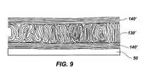
- FIG. 9is a cross-sectional view of an embodiment of the invention including a self-assembled block copolymer having polycrystalline morphology thereon.
- Self-assembling block copolymer filmsspontaneously assemble into periodic structures by microphase separation of the constituent polymer blocks after annealing, for example, by thermal annealing above the glass transition temperature of each block of the copolymer or by solvent annealing, forming domains at nanometer-scale dimensions.
- self-assembling block copolymersmay be used to create multilayer antireflective layers or coatings on a substrate.
- substrateor “semiconductor substrate” or “semiconductive substrate” or “semiconductive wafer fragment” or “wafer fragment” or “wafer” means any construction comprising semiconductor material, including, but not limited to, bulk semiconductive materials such as a semiconductive wafer (either alone or in assemblies comprising other materials).
- substratealso refers to any supporting structure including, but not limited to, glass, plastics, semiconductive substrates, wafer fragments, wafers, silicon wafers, silicon-on-insulator (“SOI”) substrates, silicon-on-sapphire (“SOS”) substrates, epitaxial layers of silicon on a base semiconductor foundation and other semiconductor materials such as silicon-germanium, germanium, gallium arsenide and indium phosphide.
- SOIsilicon-on-insulator
- SOSsilicon-on-sapphire
- Block copolymersare polymers that include one or more long sequences (i.e., “blocks”) of the same monomeric unit(s) covalently bound to one or more long sequences (i.e., “blocks”) of unlike type, for example, including differing monomeric unit(s).
- Block copolymersare conventionally named using the word “-block-” or “-b-” to separate each monomeric unit, while random copolymers are conventionally named using the term “-random-” or an “-r-” to separate each monomeric unit.
- block copolymersare contemplated herein including diblock copolymers (copolymers having two blocks), triblock copolymers (copolymers having three blocks), multiblock copolymers (copolymers having more than three blocks), and combinations thereof.
- the block copolymeris a diblock copolymer.
- Diblock copolymersmay be symmetric (i.e., the volume fraction of the first diblock copolymer is substantially the same as the volume fraction of the second block) or asymmetric (i.e., the volume fraction of the first block is substantially different than the volume fraction of the second block).
- each block of a symmetric diblock copolymerhas a volume fraction of from 0.4 to 0.6.
- each block of an asymmetric diblock copolymerhas a volume fraction less than 0.4 or greater than 0.6.
- Film morphologyincluding the size and shape of the microphase separated domains may be controlled by the molecular weight and volume fraction of the AB blocks of a diblock copolymer to produce lamellar, cylindrical or spherical morphologies, among others.
- a block copolymer filmwill microphase, separate and self-assemble into periodic spherical domains with spheres of polymer B surrounded by a matrix of polymer A.
- the diblock copolymerFor ratios of the two blocks between about 60:40 and 80:20, the diblock copolymer assembles into a periodic hexagonal close-packed or honeycombed array of cylinders of polymer B within a matrix of polymer A. For ratios between about 50:50 and 60:40, lamellar domains or alternating stripes of the blocks are formed, which is preferred for the present invention. The domain size preference depends upon the wavelength being attenuated and is generally one-fourth of the wavelength.
- the block copolymersmay self-assemble in a registered manner to create stacks of alternating planes of lamellar domains oriented substantially parallel to the substrate. In another embodiment, the block copolymers self-assemble in a polycrystalline manner to create a multitude of zones of lamellae, each zone in either a substantially parallel or substantially perpendicular orientation to an underlying substrate.
- the antireflective layersmay be sacrificial and removed, for example, at the same time as a photolithographic mask is removed. In other embodiments, the antireflective layers may remain with the final structure such as, for example, a final antireflective layer in a CMOS imager.
- a diblock copolymer 100is used as an antireflective film on a substrate to be patterned.
- a symmetric block copolymer 100may be applied to a substrate 50 by any suitable means, such as spin-coating. Creation of lamellae having a substantially parallel orientation is driven by differences in wetting interactions for each block on a given surface. Sinusoidal fluctuation in block content relative to a surface interface dampens exponentially with distance from the interface and is well understood both theoretically and experimentally. Any material that will selectively permit the diblock copolymer 100 to orient in a parallel manner to a surface thereof may be used for the surface of the substrate 50 . However, other materials may be used for the substrate 50 if the substrate is treated with a material that may permit the block copolymer to orient substantially parallel thereto. Thus, the substrate 50 is not limited to any particular material.
- the substrate 50 surfacemay be preferentially wetted by at least one block of the block copolymer.
- preferential wettingit is meant that one block of the block copolymer will wet the surface more easily than the other block(s).
- the block with the lower interfacial energy with the surfaceis the “preferentially wetting” block.
- the magnitude of preferential wettingis defined by the difference in the interfacial energies between the substrate surface and any two blocks of the block copolymer. Referring to FIG.
- the substrate 50 surfacemay be modified by depositing a polymer mat or brush 20 on the substrate surface and cross-linking the polymer mat 20 .
- the cross-linked polymer mat 20may be used, for example, to make the substrate surface preferential wetting with respect to at least one block of a block copolymer.
- the selected block copolymeris poly(styrene-b-methyl methacrylate) (PS-b-PMMA)
- PS-b-PMMApoly(styrene-b-methyl methacrylate)
- silicon oxide and clean silicon surfacesare exemplary substrates that exhibit preferential wetting toward the PMMA block to result in the assembly of a thin interface layer of PMMA as well as alternating PS and PMMA lamellae on a substrate.
- Other preferentially wetting surfaces to PMMAmay be provided, for example, by silicon nitride, SiOC, SiON, SiC, amorphous carbon, W, WSi x , TiN and resist materials such as methacrylate based components. It will be understood that such preferentially wetting materials may comprise the substrate, rather than the cross-linked polymer mat or brush 20 . Most surfaces will preferentially wet one block of a block of a block copolymer.
- FIGS. 1-3include polymer mat or brush 20 , it will be understood that this
- the polymer mat 20may be a homopolymer.
- a homopolymer of one block of the diblock copolymermay be grafted to the substrate 50 to provide a surface that is preferentially wetted by the block of the diblock copolymer that is the same as the grafted homopolymer.
- the diblock copolymer that will be self-assembledis a polystyrene-b-polymethylmethacrylate diblock copolymer
- a polystyrene homopolymermay be grafted to the substrate to provide a surface that is preferentially wetted by the polystyrene block of the diblock copolymer; or a polymethylmethacrylate homopolymer may be grafted to the substrate to provide a surface that is preferentially wetted by the polymethylmethacrylate block of the diblock copolymer.
- the homopolymersmay be grafted by a wide variety of methods known in the art including, for example, preparing homopolymers with end groups (e.g., hydroxyl groups) that may interact (e.g., by forming hydrogen and/or covalent bonds) with the silicon-containing surface.
- end groupse.g., hydroxyl groups
- polymer mat 20may be cross-linked, for example, by exposure to radiation, e.g., ultraviolet (UV) radiation.
- the polymer mat 20 being cross-linkedmay be susceptible to cross-linking without the addition of a cross-linking agent.
- the polymer mat 20is a polystyrene-r-polymethylmethacrylate random copolymer
- the polystyrene in the random copolymermay be a cross-linking site upon exposure to UV radiation.
- a small amounte.g., 1 mole % to 5 mole %) of thermally cross-linkable monomer (e.g., a benzocyclobutane-containing monomer) or a photochemically cross-linkable monomer (e.g., divinyl benzene) may be included in the polymer mat 20 .
- a cross-linking agentcan be added to polymer mat 20 .
- cross-linking agentsinclude, for example, the combination of a cross-linker (e.g., 1,3,5-trimethyl-2,4,6-(triacetoxymethyl)benzene) and a thermal acid generator (e.g., cyclohexylmethyl(2-oxocyclohexyl)sulfonium trifluoromethanesulfonate).
- a cross-linkere.g., 1,3,5-trimethyl-2,4,6-(triacetoxymethyl)benzene
- a thermal acid generatore.g., cyclohexylmethyl(2-oxocyclohexyl)sulfonium trifluoromethanesulfonate.
- the cross-linked polymer mat 20preferably has resistance adequate to withstand further processing steps encountered during the block copolymer self-assembly.
- the blocks of the block copolymermay be polybutadiene-polybutylmethacrylate, polybutadiene-polydimethylsiloxane, poly(styrene-b-methyl methacrylate) (PS-b-PMMA), polybutadiene-polymethylmethacrylate, polybutadiene-polyvinylpyridine, polybutylmethacrylate-polybutylacrylate, polybutylmethacrylate-polyvinylpyridine, polybutadiene-polyvinylpyridine, polyethyleneoxide-polyisoprene, polyethyleneoxide-polybutadiene, polyethyleneoxide-polystyrene, polyethylene-polyvinylpyridine, polyisoprene-polymethylmethacrylate, polyisoprene-polyvinylpyridine, polybutylacrylate-polymethylmethacrylate, polybutylacrylate-poly
- the block copolymermay be a diblock copolymer.
- block copolymers having three (a triblock copolymer) or more (a multiblock copolymer) blocksmay also be used.
- triblock copolymersinclude, but are not limited to, poly(styrene-block-methyl methacrylate-block-ethylene oxide) and block copolymers having three or more blocks selected from the following: polystyrene, polymethylmethacrylate, polyethyleneoxide, polyisoprene, polybutadiene, poly lactic acid, polyvinylpyridine, and combinations thereof.
- the block copolymer materialmay also be formulated as a binary, tertiary or ternary blend comprising a self-assembling block copolymer and one or more homopolymers of the same type of polymers as the polymer blocks in the block copolymer, to produce blends that swell the size of the polymers domains and increase the L o value of the polymer.
- the volume fraction of the homopolymersmay range from 0% to 40%.
- An exemplary ternary diblock copolymer blendis a PS-b-PMMA/PS/PMMA blend, for example, 18K/18K, 25K/26K or 37K/37K PS-b-PMMA containing 40% 20K polystyrene and 20K poly(methylmethacrylate).
- the block copolymer 100may be applied to the substrate 50 to a thickness “L” by conventional techniques including, for example, deposition methods, coating methods, transfer methods, and/or other available application methods.
- the block copolymer 100may be applied by spin-coating, dip coating, spray coating, and combinations thereof.
- the block copolymer 100may be dissolved, dispersed, or suspended in a medium (e.g., a solvent).
- the solution, dispersion, or suspensionmay be deposited on the substrate 50 , and the medium may be optionally removed (e.g., through evaporation at ambient or elevated temperature, and at ambient or reduced pressure) during or subsequent to deposition.
- the diblock copolymer 100may be annealed to break up existing domains and allow the diblock copolymer 100 to self-assemble ( FIG. 2 ).
- the diblock copolymer 100may be annealed by thermal annealing, solvent annealing or a combination thereof. During the annealing, the block polymer may form ordered domains.
- Thermal annealingmay include exposing the diblock copolymer to an elevated temperature (e.g., at or above the glass transition temperature of the diblock copolymer), and, after self-assembly, lowering the temperature to allow the self-assembled diblock copolymer to harden.
- the block polymermay be thermally annealed by heating the diblock copolymer to a temperature of from about 0° C. to about 250° C. for up to about 24 hours or longer, preferably under a vacuum or inert atmosphere.
- Solvent annealingmay include exposing the diblock copolymer to a solvent until the block copolymer swells. At least a portion of the solvent may then be removed, such as through evaporation.
- Chiis an interaction parameter that indicates how chemically distinct each block of the block copolymers is and the energetic cost of mixing the blocks; X*N determines whether the blocks will microphase separate (where N is the chain length of the monomer).
- the layersassume a sinusoidal orientation relative to the interface.
- the sinusoidal effectmay be adjusted by selecting a preferential wetting surface and by selecting each block of the block copolymer, based on conventional knowledge, such that the blocks separate rather than intermingle.
- each block of the diblock copolymer 100may self-assemble and form alternating lamellae 110 and 120 that are substantially parallel to a major plane of the substrate 50 .
- the alternating lamellae 110 and 120form multilayer antireflection coating 200 .
- substantially parallel lamellaerefers to a set of lamellae that are, on average, parallel to the surface.
- lamellae 110 and 120have different indices of refraction.
- at least three (3) to six (6) layers of alternating lamellaeare formed. More preferably, at least three (3) to twenty (20) layers of alternating lamellae are formed.
- a three-layered structure formed from diblock copolymer ABwould includes layers (or lamellae) A/B/A.
- the diblock copolymersform substantially continuous, or nonporous, layers on the substrate surface.
- one or more blocks of the block copolymermay form porous layers on the substrate surface.
- Symmetric diblock copolymersself-assemble into lamellar structures in which alternating lamellae each represent a domain including one block of the diblock copolymer.
- the distance between the middle of a first domain and the middle of the next domain of the same block typeis the inherent periodicity (L o ) of the diblock copolymer, which is dependent on the length and/or molecular weight of the polymer chain for each block ( FIG. 2 ).
- the inherent periodicitymay be increased by increasing the length and/or molecular weight of the polymer chain for one or both blocks of a diblock copolymer.
- the L omay be decreased by decreasing the length and/or molecular weight of the polymer chain for one or both blocks of a block copolymer.
- Block copolymers contemplated hereinmay have an L o from about 10 nanometers to 100 nanometers.
- the L o of the first block copolymermay be the same as or different from the L o of the second block copolymer.
- the desired thicknessdepends on the degree of ordering relative to an interface. If the lamellae are substantially parallel to the substrate 50 throughout the film, then the thickness of the block copolymer is selected to match the pitch (inherent periodicity). Preferential thickness is either an integral multiple of pitch L o ( ⁇ L o ) or off by one-half L o (where (n+1 ⁇ 2)L o ) depending on preferential interface wetting.
- the preferred thicknessis ⁇ L o
- thickness of (n+1 ⁇ 2)L o )is preferred. If the lamellae are not substantially parallel to the surface throughout films above a certain thickness, then the films may be any thickness above that minimal value as the regions that are not substantially parallel may be any thickness without an energetic cost.
- lamellae 110 and/or 120may be optionally cross-linked, for example, by exposure to radiation, e.g., ultraviolet (UV) radiation.
- the block(s) of the block copolymer being cross-linkedmay be susceptible to cross-linking without the addition of cross-linking agent.
- the block copolymeris a polystyrene-b-polymethylmethacrylate diblock copolymer
- the polystyrene blockmay be cross-linked by exposure to UV radiation.
- one block of the block copolymermay be made cross-linkable by including a small amount (e.g., 1 mole % to 5 mole %) of thermally cross-linkable monomer (e.g., a benzocyclobutane-containing monomer) or a photochemically cross-linkable monomer (e.g., divinyl benzene) in the block of the copolymer.
- thermally cross-linkable monomere.g., a benzocyclobutane-containing monomer
- a photochemically cross-linkable monomere.g., divinyl benzene
- cross-linking agentcan be added to the lamellae that are to be cross-linked.
- cross-linking agentsinclude, for example, the combination of a cross-linker (e.g., 1,3,5-trimethyl-2,4,6-(triacetoxymethyl)benzene) and a thermal acid generator (e.g., cyclohexylmethyl(2-oxocyclohexyl)sulfonium trifluoromethanesulfonate).
- a cross-linkere.g., 1,3,5-trimethyl-2,4,6-(triacetoxymethyl)benzene
- a thermal acid generatore.g., cyclohexylmethyl(2-oxocyclohexyl)sulfonium trifluoromethanesulfonate.
- a cross-linked domainmay have, for example, improved mechanical robustness.
- the first block copolymer and the second block copolymerpreferably have different refractive indexes.
- Each block of a block copolymermay differ from other blocks in the copolymer not only in terms of the structure of monomeric units that form that block, but also in other properties including, for example, physical properties (e.g., mechanical strength, surface tension, wettability, and/or solubility) and chemical properties (e.g., solubility, refractive index, chemical reactivity, susceptibility to removal techniques and/or susceptibility to cross-linking reactions).
- Chain length of each block copolymermay be conventionally selected based on the desired wavelength to be reflected.
- At least one block of a block copolymermay be optionally doped or otherwise modified to alter its refractive index.
- dyes or inorganic materialsmay be incorporated into at least one block of the block copolymer prior to casting.
- a water-insoluble photochromic dyemay be incorporated into a hydrophobic core of a block copolymer.
- metal-functional monomersmay be polymerized to form metal-containing block copolymers.
- preformed copolymersmay be directly blended with metallic nanoparticles, nanoclusters or quantum dots.
- ligand functional polymersmay be prepared by either direct polymerization of ligand functional monomers or by the post-polymerization modification of appropriate precursor polymers.
- a film of annealed, parallel lamellae of polystyrene-b-poly(4-vinylpyridine)may be exposed to a poly(4-vinylpyridine)-selective solvent containing gold molecules.
- the goldis thus selectively placed in the poly(4-vinylpyridine) domains.
- the filmmay then be further exposed to a poly(4-vinylpyridine)-selective solvent containing a reducing agent, which converts the gold molecules to gold nanoparticles in the poly(4-vinylpyridine) domains.
- one block of a block copolymermay be exposed to vapors of a metallic species such that the metallic species is selectively incorporated into one block of the block copolymer prior to forming the block copolymer.
- a block copolymerfor example, PS-b-PMMA or poly(hydroxylated isoprene
- PS-PPESpolystyrene-b-poly(4-phenylethynylstyrene)
- PS-PPESpolystyrene-b-poly(4-phenylethynylstyrene)
- Exemplary metal speciesinclude, but are not limited to, gold, platinum, cobalt, iron, palladium, nickel, copper, zinc, ruthenium, silver, rhodium, aluminum, yttrium, chromium, manganese, vanadium, tin, and rhenium. Doping one block of the diblock copolymer with an inorganic material assists in the segregation of the blocks into separate domains and varies the optical properties of the resulting film, which improves the performance of the antireflective layer.
- photoresist 150may be patterned on an upper surface of the multilayer antireflection coating 200 for conventional photo-imaging. Selected areas of photoresist may be exposed to radiation from a light source to form a desired pattern on the photoresist by conventional techniques.
- the multilayer antireflection coating 200will absorb light that has reflected back from the substrate surface, thereby inhibiting the light from traveling through the photoresist.
- the multilayered composition of the antireflection layerincreases the amount of light that is absorbed by the antireflection layer.
- the amount of absorbed lightmay also be increased.
- the photoresist 150 and antireflection layermay be removed by conventional techniques resulting in a patterned substrate.
- An antireflection layer including multiple, planar layersis best suited for applications in which the light contacts the antireflection layer in a substantially perpendicular orientation.
- an antireflection layer configured to attenuate light from a multitude of anglesmay also be useful when patterning a substrate.
- a block copolymer 100may be applied to a substrate 50 where the domain size “L 1 ” (thickness) of each block over a substrate is ⁇ /4 (where ⁇ is the wavelength used) ( FIG. 4 ).
- An annealing stepmay be performed, but is not required provided that adequate self-assembly occurs during spin-coating. The volatility of the solvent used for spin-coating will impact this.
- Thin films prepared on a neutral-wetting substrate and annealeddo not have any preferential orientation of domains and will assemble into a disordered fingerprint-like structure despite extensive annealing as shown in FIG. 5 .
- domainsare created such that a first domain 130 is oriented substantially perpendicular to a major plane of the underlying substrate 50 and a second domain 140 is oriented substantially parallel to the major plane of substrate 50 .
- the self-assembled polymer in the center of the filmis mostly oriented in a quasi-perpendicular morphology 130 ′ relative to substrate 50 , with some bending and the formation of T-junctions where the parallel and perpendicular regions overlap.
- a complementary metal oxide semiconductor (CMOS) imagerincludes a multilayer antireflection coating including self-assembled block copolymers.
- the preliminary process steps of forming a CMOS imagermay proceed by conventional methods.
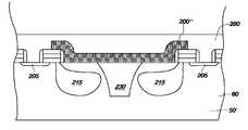
- FIG. 6illustrates an exemplary view of a portion of a conventional CMOS image sensor four-transistor (4T) pixel.
- the exemplary CMOS image sensorincludes two adjacent pixels 250 , 255 and a light-sensing element, shown as a photodiode 210 , that may be formed having a photosensitive p-n junction region comprising a p-type surface layer 225 and an n-type photodiode region 215 within a p-type region 60 .
- P-type region 60may be formed on substrate 50 ′.
- the light-sensing elementis not restricted to a photodiode, but may be selected from any light-sensing element including, without limitation, photogates, pinned photodiodes, partially pinned photodiodes, etc.
- the self-assembled block copolymer antireflection coatingmay be incorporated into any CMOS or CCD (charge-coupled device) image sensors.
- photodiodes 210may be separated by isolation region 230 , for example, a field oxide or short trench isolation.
- the trench isolation regionmay be conventionally formed in a p-well active layer in a p-type region 60 adjacent to n-type photodiode region 215 to isolate the pixels 250 , 255 .
- the n-type photodiode region 215may function as a charge collection region of a photodiode 210 for collecting charges generated by light incident on a pixel.
- a conventional CMOS image sensormay also include a transfer transistor having a gate 220 for transferring photoelectric charges from the charge collection region to the floating diffusion region 205 .
- the CMOS image sensormay also include a reset transistor having a gate 240 . It will be understood that gate stacks for the pixel transistors may be formed before or after the trench isolation regions are formed. The order of these preliminary process steps may be varied as is required or convenient for a particular process flow.
- a multilayer antireflection layer or coating 200 ′may be used to minimize the amount of light reflected from the photodiode 210 .
- a block copolymermay be deposited over the CMOS image sensor as described herein. In one embodiment, the block copolymer is deposited to a thickness of 1 ⁇ m to 10 ⁇ m. In an embodiment depicted in FIG. 7 , the block copolymer may be cast under conditions that allow the block copolymer to self-assemble into lamellae that are substantially parallel to the underlying substrate 50 ′.
- a polymer mat 20 ′may be required to create a preferential wetting surface for the block copolymer.
- the block copolymermay be annealed to form a multilayer antireflection coating 200 ′ and then selectively etched, or otherwise patterned, such that the multilayer antireflection coating 200 ′ is only present over the photodiode 210 .
- the block copolymermay be annealed to form a multilayer antireflection coating 200 ′ over the entire device.
- the CMOS imagermay then be subjected to further conventional processing such as, for example, deposition of an oxide layer thereover.
- the antireflection coating 200 ′′includes a plurality of block copolymer domains randomly oriented either parallel or perpendicular to the major plane of an underlying substrate 50 ′.
- a block copolymermay be applied to the substrate 50 ′ at a thickness of 1 ⁇ m to 100 ⁇ m and an annealing step may be optionally performed. Thin films prepared on a flat substrate and annealed do not have any preferential orientation of domains and will assemble into a disordered fingerprint-like structure despite extensive annealing as shown and described in FIG. 5 .
- the CMOS imagermay then be subjected to further conventional processing such as, for example, deposition of an oxide layer 280 thereover.
- the filmis thermally annealed above the glass transition temperature of the blocks under an inert atmosphere for sufficient time to induce ordered self-assembly relative to the substrate and air interfaces, e.g., 24 hours at 250° C.
- the lamellar structuresassemble so that PMMA wets the substrate interface and PS wets the air interface to form ten and one-half periods or twenty total PS-PMMA interfaces with a domain size for each lamellar plane of 15 nm.
- the L o value(and corresponding domain size) may be increased by using either higher molecular weight block copolymer or creating a ternary blend of the PS-PMMA block copolymer with homopolymers of PS and PMMA. If the difference in interfacial energies for PS and PMMA with the substrate is >0.75 ergs/cm 2 , the number of periods in the film may be increased in proportion with the increase in surface energy differential.
- the filmis thermally annealed above the glass transition temperature of the blocks under an inert atmosphere for sufficient time to induce ordered self-assembly relative to the substrate and air interfaces, e.g., 24 hours at 250° C.
- the lamellar structuresassemble so that PMMA wets the substrate interface to a distance of ⁇ 3 pitches (six PS-PMMA interfaces) with 100% parallel domains, and PS wets the air interface to form two to three pitches (four to six PS-PMMA interfaces) of 100% parallel domains relative to the air interface.
- the self-assembled polymer in the center of the filmis mostly oriented in a quasi-perpendicular morphology relative to the substrate, with some bending and the formation of T-junctions where the parallel and perpendicular regions overlap (see, e.g., FIG. 9 ).
- the L o value (and corresponding domain size)can be increased by using either higher molecular weight block copolymer or creating a ternary blend of the PS-PMMA block copolymer with homopolymers of PS and PMMA.
- a substrateis grafted with a random PS-r-PMMA copolymer with a fractional mol % of PS of ⁇ 60% such that the surface energy differential for homopolymers of PS and PMMA is around 0.0625 ergs/cm 2 .
- the composition of the blendis defined so that for a given total film thickness spun-cast from a solution of the blend over a nanometer-square area, the ( ⁇ -perfluorodacanoyl- ⁇ -TEMPO)-PS-r-PMMA will account for 6 nm 3 of the volume of film.
- the blended filmis thermally annealed above the glass transition temperature of the blocks under an inert atmosphere for sufficient time to induce ordered self-assembly relative to the substrate and air interfaces, e.g., 24 hours at 250° C.; the ( ⁇ -perfluorodacanoyl- ⁇ -TEMPO)-PS-r-PMMA will phase segregate to the air interface selectively.
- the surface energy differentials for the block copolymer at the surface and “air” interfacesare projected to provide no exclusive bias toward either parallel or perpendicular structures, and so the bounded block copolymer thin film will self-assemble as the material in bulk, with no long-range ordering or preferred orientation to interfaces (see, e.g., FIG. 5 ).
- the lamellar structuresself-assemble so that a P4VP domain wets the substrate interface and a PS domain wets the air interface, forming ten interfaces between the domains in the film.
- the filmis soaked in a 1% solution of hydrogen tetrachloroaurate(III) ⁇ HAuCl 4 ⁇ in ethanol for up to 10 minutes; this selectively impregnates the P4VP domains with gold species.
- the filmis then placed in a 1% solution of sodium borohydride ⁇ NaBH 4 ⁇ in ethanol for up to 30 seconds to reduce the hydrogen tetrachloroaurate to gold nanoparticles ⁇ 3 nm in diameter located exclusively in the P4VP domains.
Landscapes
- Engineering & Computer Science (AREA)
- Physics & Mathematics (AREA)
- General Physics & Mathematics (AREA)
- Manufacturing & Machinery (AREA)
- Microelectronics & Electronic Packaging (AREA)
- Health & Medical Sciences (AREA)
- Computer Hardware Design (AREA)
- Power Engineering (AREA)
- Condensed Matter Physics & Semiconductors (AREA)
- Life Sciences & Earth Sciences (AREA)
- General Health & Medical Sciences (AREA)
- Molecular Biology (AREA)
- Architecture (AREA)
- Structural Engineering (AREA)
- Optics & Photonics (AREA)
- Laminated Bodies (AREA)
Abstract
Description
Claims (15)
Priority Applications (5)
| Application Number | Priority Date | Filing Date | Title |
|---|---|---|---|
| US11/766,663US8294139B2 (en) | 2007-06-21 | 2007-06-21 | Multilayer antireflection coatings, structures and devices including the same and methods of making the same |
| US13/157,838US8956713B2 (en) | 2007-04-18 | 2011-06-10 | Methods of forming a stamp and a stamp |
| US13/613,358US8551808B2 (en) | 2007-06-21 | 2012-09-13 | Methods of patterning a substrate including multilayer antireflection coatings |
| US14/176,574US9276059B2 (en) | 2007-04-18 | 2014-02-10 | Semiconductor device structures including metal oxide structures |
| US15/044,713US9768021B2 (en) | 2007-04-18 | 2016-02-16 | Methods of forming semiconductor device structures including metal oxide structures |
Applications Claiming Priority (1)
| Application Number | Priority Date | Filing Date | Title |
|---|---|---|---|
| US11/766,663US8294139B2 (en) | 2007-06-21 | 2007-06-21 | Multilayer antireflection coatings, structures and devices including the same and methods of making the same |
Related Child Applications (1)
| Application Number | Title | Priority Date | Filing Date |
|---|---|---|---|
| US13/613,358DivisionUS8551808B2 (en) | 2007-04-18 | 2012-09-13 | Methods of patterning a substrate including multilayer antireflection coatings |
Publications (2)
| Publication Number | Publication Date |
|---|---|
| US20080315270A1 US20080315270A1 (en) | 2008-12-25 |
| US8294139B2true US8294139B2 (en) | 2012-10-23 |
Family
ID=40135559
Family Applications (2)
| Application Number | Title | Priority Date | Filing Date |
|---|---|---|---|
| US11/766,663Active2030-05-06US8294139B2 (en) | 2007-04-18 | 2007-06-21 | Multilayer antireflection coatings, structures and devices including the same and methods of making the same |
| US13/613,358ActiveUS8551808B2 (en) | 2007-04-18 | 2012-09-13 | Methods of patterning a substrate including multilayer antireflection coatings |
Family Applications After (1)
| Application Number | Title | Priority Date | Filing Date |
|---|---|---|---|
| US13/613,358ActiveUS8551808B2 (en) | 2007-04-18 | 2012-09-13 | Methods of patterning a substrate including multilayer antireflection coatings |
Country Status (1)
| Country | Link |
|---|---|
| US (2) | US8294139B2 (en) |
Cited By (29)
| Publication number | Priority date | Publication date | Assignee | Title |
|---|---|---|---|---|
| US8551808B2 (en) | 2007-06-21 | 2013-10-08 | Micron Technology, Inc. | Methods of patterning a substrate including multilayer antireflection coatings |
| US8557128B2 (en) | 2007-03-22 | 2013-10-15 | Micron Technology, Inc. | Sub-10 nm line features via rapid graphoepitaxial self-assembly of amphiphilic monolayers |
| US8609221B2 (en) | 2007-06-12 | 2013-12-17 | Micron Technology, Inc. | Alternating self-assembling morphologies of diblock copolymers controlled by variations in surfaces |
| US8633112B2 (en) | 2008-03-21 | 2014-01-21 | Micron Technology, Inc. | Thermal anneal of block copolymer films with top interface constrained to wet both blocks with equal preference |
| US8642157B2 (en) | 2008-02-13 | 2014-02-04 | Micron Technology, Inc. | One-dimensional arrays of block copolymer cylinders and applications thereof |
| US8641914B2 (en) | 2008-03-21 | 2014-02-04 | Micron Technology, Inc. | Methods of improving long range order in self-assembly of block copolymer films with ionic liquids |
| US8753738B2 (en) | 2007-03-06 | 2014-06-17 | Micron Technology, Inc. | Registered structure formation via the application of directed thermal energy to diblock copolymer films |
| US8785559B2 (en) | 2007-06-19 | 2014-07-22 | Micron Technology, Inc. | Crosslinkable graft polymer non-preferentially wetted by polystyrene and polyethylene oxide |
| US8900963B2 (en) | 2011-11-02 | 2014-12-02 | Micron Technology, Inc. | Methods of forming semiconductor device structures, and related structures |
| US8956713B2 (en) | 2007-04-18 | 2015-02-17 | Micron Technology, Inc. | Methods of forming a stamp and a stamp |
| US8993088B2 (en) | 2008-05-02 | 2015-03-31 | Micron Technology, Inc. | Polymeric materials in self-assembled arrays and semiconductor structures comprising polymeric materials |
| WO2015048244A1 (en)* | 2013-09-25 | 2015-04-02 | Cornell University | Multiblock copolymer films with inorganic nanoparticles, methods of making same, and uses thereof |
| US8999492B2 (en) | 2008-02-05 | 2015-04-07 | Micron Technology, Inc. | Method to produce nanometer-sized features with directed assembly of block copolymers |
| US20150160072A1 (en)* | 2013-12-06 | 2015-06-11 | Rensselaer Polytechnic Institute | Oriented backscattering wide dynamic-range optical radiation sensor |
| US9087699B2 (en) | 2012-10-05 | 2015-07-21 | Micron Technology, Inc. | Methods of forming an array of openings in a substrate, and related methods of forming a semiconductor device structure |
| US9142420B2 (en) | 2007-04-20 | 2015-09-22 | Micron Technology, Inc. | Extensions of self-assembled structures to increased dimensions via a “bootstrap” self-templating method |
| US9177795B2 (en) | 2013-09-27 | 2015-11-03 | Micron Technology, Inc. | Methods of forming nanostructures including metal oxides |
| KR20150125291A (en)* | 2014-04-30 | 2015-11-09 | 현대자동차주식회사 | Method for manufacturing of substrate and substrate |
| US9229328B2 (en) | 2013-05-02 | 2016-01-05 | Micron Technology, Inc. | Methods of forming semiconductor device structures, and related semiconductor device structures |
| US9276059B2 (en) | 2007-04-18 | 2016-03-01 | Micron Technology, Inc. | Semiconductor device structures including metal oxide structures |
| US10059622B2 (en) | 2012-05-07 | 2018-08-28 | Guardian Glass, LLC | Anti-reflection glass with tin oxide nanoparticles |
| US10345702B2 (en) | 2017-08-24 | 2019-07-09 | International Business Machines Corporation | Polymer brushes for extreme ultraviolet photolithography |
| US11401411B2 (en) | 2016-11-17 | 2022-08-02 | Terapore Technologies, Inc. | Isoporous self-assembled block copolymer films containing high molecular weight hydrophilic additives and methods of making the same |
| US11466134B2 (en) | 2011-05-04 | 2022-10-11 | Cornell University | Multiblock copolymer films, methods of making same, and uses thereof |
| US11567072B2 (en) | 2017-02-22 | 2023-01-31 | Terapore Technologies, Inc. | Ligand bound MBP membranes, uses and method of manufacturing |
| US11571667B2 (en) | 2018-03-12 | 2023-02-07 | Terapore Technologies, Inc. | Isoporous mesoporous asymmetric block copolymer materials with macrovoids and method of making the same |
| US11572424B2 (en) | 2017-05-12 | 2023-02-07 | Terapore Technologies, Inc. | Chemically resistant fluorinated multiblock polymer structures, methods of manufacturing and use |
| US11628409B2 (en) | 2016-04-28 | 2023-04-18 | Terapore Technologies, Inc. | Charged isoporous materials for electrostatic separations |
| US12109541B2 (en) | 2017-09-19 | 2024-10-08 | Terapore Technologies, Inc. | Chemically resistant isoporous crosslinked block copolymer structure |
Families Citing this family (27)
| Publication number | Priority date | Publication date | Assignee | Title |
|---|---|---|---|---|
| US8394483B2 (en) | 2007-01-24 | 2013-03-12 | Micron Technology, Inc. | Two-dimensional arrays of holes with sub-lithographic diameters formed by block copolymer self-assembly |
| US8114300B2 (en)* | 2008-04-21 | 2012-02-14 | Micron Technology, Inc. | Multi-layer method for formation of registered arrays of cylindrical pores in polymer films |
| US8247033B2 (en) | 2008-09-19 | 2012-08-21 | The University Of Massachusetts | Self-assembly of block copolymers on topographically patterned polymeric substrates |
| US8211737B2 (en) | 2008-09-19 | 2012-07-03 | The University Of Massachusetts | Method of producing nanopatterned articles, and articles produced thereby |
| US8518837B2 (en) | 2008-09-25 | 2013-08-27 | The University Of Massachusetts | Method of producing nanopatterned articles using surface-reconstructed block copolymer films |
| US8003521B2 (en) | 2009-04-07 | 2011-08-23 | Micron Technology, Inc. | Semiconductor processing |
| JP2013508351A (en)* | 2009-10-22 | 2013-03-07 | ロレアル | Photoprotective composition and film, and production method |
| US8828493B2 (en)* | 2009-12-18 | 2014-09-09 | International Business Machines Corporation | Methods of directed self-assembly and layered structures formed therefrom |
| US8304493B2 (en) | 2010-08-20 | 2012-11-06 | Micron Technology, Inc. | Methods of forming block copolymers |
| US9156682B2 (en) | 2011-05-25 | 2015-10-13 | The University Of Massachusetts | Method of forming oriented block copolymer line patterns, block copolymer line patterns formed thereby, and their use to form patterned articles |
| FR2975823B1 (en)* | 2011-05-27 | 2014-11-21 | Commissariat Energie Atomique | METHOD FOR MAKING A PATTERN ON THE SURFACE OF A BLOCK OF A SUBSTRATE USING BLOCK COPOLYMERS |
| KR102013503B1 (en)* | 2011-09-28 | 2019-08-22 | 뷔흘러 알제나우 게엠베하 | Method and apparatus for producing a reflection-reducing layer on an substrate |
| US9257478B2 (en)* | 2012-05-22 | 2016-02-09 | The Regents Of The University Of California | Spatially resolved spectral-imaging device |
| JP6239813B2 (en) | 2012-07-18 | 2017-11-29 | 株式会社Screenセミコンダクターソリューションズ | Substrate processing apparatus and substrate processing method |
| US9656294B2 (en)* | 2012-11-20 | 2017-05-23 | Massachusetts Institute Of Technology | Fabrication and passivation of silicon surfaces |
| US11906868B2 (en) | 2013-12-24 | 2024-02-20 | View, Inc. | Obscuring bus bars in electrochromic glass structures |
| US10884311B2 (en) | 2013-12-24 | 2021-01-05 | View, Inc. | Obscuring bus bars in electrochromic glass structures |
| WO2017112685A1 (en)* | 2015-12-21 | 2017-06-29 | View, Inc. | Obscuring bus bars in electrochromic glass structures |
| CN105814271B (en) | 2013-12-24 | 2019-03-22 | 唯景公司 | Masking bus bars in electrochromic glass structures |
| FR3031750B1 (en)* | 2015-01-21 | 2018-09-28 | Arkema France | PROCESS FOR OBTAINING THICK ORDERED FILMS AND HIGH PERIODS COMPRISING A BLOCK COPOLYMER |
| CN105140416B (en)* | 2015-08-12 | 2017-11-10 | 京东方科技集团股份有限公司 | Scattering layer and preparation method thereof, its obtained organic LED display device |
| US11952486B2 (en) | 2017-04-25 | 2024-04-09 | Avient Corporation | Thermoplastic elastomer compounds exhibiting retained clarity and improved surface structure |
| US11667785B2 (en) | 2017-04-25 | 2023-06-06 | Avient Corporation | Thermoplastic elastomer compounds exhibiting improved stain resistance |
| US11725275B2 (en) | 2017-07-13 | 2023-08-15 | Uchicago Argonne, Llc | Low refractive index surface layers and related methods |
| US10312200B2 (en) | 2017-07-27 | 2019-06-04 | International Business Machines Corporation | Integrated circuit security |
| US11320738B2 (en)* | 2018-06-27 | 2022-05-03 | Taiwan Semiconductor Manufacturing Co., Ltd. | Pattern formation method and material for manufacturing semiconductor devices |
| FR3113409B1 (en)* | 2020-08-17 | 2022-07-22 | Commissariat Energie Atomique | METHOD FOR MAKING A QUANTUM DEVICE WITH NUCLEAR SPIN QUBITS |
Citations (90)
| Publication number | Priority date | Publication date | Assignee | Title |
|---|---|---|---|---|
| US4797357A (en) | 1986-05-30 | 1989-01-10 | Eastman Kodak Company | Light-stable reducible compounds and analytical compositions, elements and methods utilizing same |
| US5512131A (en) | 1993-10-04 | 1996-04-30 | President And Fellows Of Harvard College | Formation of microstamped patterns on surfaces and derivative articles |
| US5580700A (en) | 1992-11-25 | 1996-12-03 | Hoechst Celanese Corporation | Metal ion reduction in bottom anti-reflective coatings for use in semiconductor device formation |
| US5620850A (en) | 1994-09-26 | 1997-04-15 | President And Fellows Of Harvard College | Molecular recognition at surfaces derivatized with self-assembled monolayers |
| US5772905A (en) | 1995-11-15 | 1998-06-30 | Regents Of The University Of Minnesota | Nanoimprint lithography |
| US5879853A (en) | 1996-01-18 | 1999-03-09 | Kabushiki Kaisha Toshiba | Top antireflective coating material and its process for DUV and VUV lithography systems |
| US5948470A (en) | 1997-04-28 | 1999-09-07 | Harrison; Christopher | Method of nanoscale patterning and products made thereby |
| US5958704A (en) | 1997-03-12 | 1999-09-28 | Ddx, Inc. | Sensing system for specific substance and molecule detection |
| US6207787B1 (en) | 1994-07-27 | 2001-03-27 | International Business Machines Corporation | Antireflective coating for microlithography |
| US20010024768A1 (en) | 1996-02-26 | 2001-09-27 | Matsushita Electric Industrial Co., Ltd. | Pattern forming material and pattern forming method |
| US6309580B1 (en) | 1995-11-15 | 2001-10-30 | Regents Of The University Of Minnesota | Release surfaces, particularly for use in nanoimprint lithography |
| WO2002018080A1 (en) | 2000-08-03 | 2002-03-07 | Upepo & Maji Inc. | Metal colloidal solution composition and conductor or ink for forming semiconductor pattern comprising it and method for forming conductor or semiconductor pattern |
| US6414164B1 (en) | 2000-07-12 | 2002-07-02 | International Business Machines Corporation | Synthesis of soluble derivatives of sexithiophene and their use as the semiconducting channels in thin-film filed-effect transistors |
| US6423474B1 (en) | 2000-03-21 | 2002-07-23 | Micron Technology, Inc. | Use of DARC and BARC in flash memory processing |
| US6506660B2 (en) | 2000-11-15 | 2003-01-14 | International Business Machines Corporation | Semiconductor with nanoscale features |
| US6518194B2 (en) | 2000-12-28 | 2003-02-11 | Thomas Andrew Winningham | Intermediate transfer layers for nanoscale pattern transfer and nanostructure formation |
| US6517933B1 (en) | 2000-01-18 | 2003-02-11 | Nano-Tex, Llc | Hybrid polymer materials |
| US6537920B1 (en) | 2001-03-16 | 2003-03-25 | Advanced Micro Devices, Inc. | Formation of vertical transistors using block copolymer lithography |
| US20030068639A1 (en) | 2001-08-31 | 2003-04-10 | Thomas Haneder | Detecting biochemical reactions |
| US20030080471A1 (en) | 2001-10-29 | 2003-05-01 | Chou Stephen Y. | Lithographic method for molding pattern with nanoscale features |
| US6565764B2 (en) | 2000-08-11 | 2003-05-20 | Kabushiki Kaisha Toshiba | Method of manufacturing a material having a fine structure |
| WO2003045840A2 (en) | 2001-11-21 | 2003-06-05 | University Of Massachusetts | Mesoporous materials and methods |
| US20030108879A1 (en) | 2001-01-10 | 2003-06-12 | Symyx Technologies, Inc. | Polymer brushes for immobilizing molecules to a surface or substrate having improved stability |
| US6592764B1 (en) | 1997-12-09 | 2003-07-15 | The Regents Of The University Of California | Block copolymer processing for mesostructured inorganic oxide materials |
| US6635912B2 (en) | 2000-09-07 | 2003-10-21 | Nec Electronics Corporation | CMOS image sensor and manufacturing method thereof |
| US6656308B2 (en) | 2002-04-22 | 2003-12-02 | International Business Machines Corporation | Process of fabricating a precision microcontact printing stamp |
| US20030235930A1 (en) | 2002-06-25 | 2003-12-25 | Lucent Technologies Inc. | Multi-impression nanofeature production |
| US6679996B1 (en) | 1999-10-05 | 2004-01-20 | Hoya Corporation | Metal oxide pattern forming method |
| US20040058059A1 (en) | 2001-11-07 | 2004-03-25 | Linford Mathew Richard | Funtionalized patterned surfaces |
| US20040124092A1 (en) | 2002-12-30 | 2004-07-01 | Black Charles T. | Inorganic nanoporous membranes and methods to form same |
| US20040142578A1 (en) | 2002-03-28 | 2004-07-22 | Ulrich Wiesner | Thin film nanostructures |
| US6780492B2 (en) | 1999-03-02 | 2004-08-24 | International Business Machines Corporation | Substrates prepared by chemical amplification of self-assembled monolayers with spatially localized polymer brushes |
| US20040163758A1 (en) | 2000-04-21 | 2004-08-26 | International Business Machines Corporation | Patterning solution deposited thin films with self-assembled monolayers |
| US6812132B2 (en) | 2003-03-21 | 2004-11-02 | Intel Corporation | Filling small dimension vias using supercritical carbon dioxide |
| US20040256615A1 (en)* | 2001-07-09 | 2004-12-23 | Henning Sirringhaus | Lamellar polymer architecture |
| JP2005029779A (en) | 1999-06-07 | 2005-02-03 | Toshiba Corp | Pattern forming material, pattern forming method, method for producing porous structure, electrochemical cell, method for producing porous carbon structure, and porous carbon structure |
| US20050079486A1 (en) | 2003-09-23 | 2005-04-14 | Wiscnsin Alumni Research Foundation - | Using liquid crystals to detect affinity microcontact printed biomolecules |
| US6887332B1 (en) | 2000-04-21 | 2005-05-03 | International Business Machines Corporation | Patterning solution deposited thin films with self-assembled monolayers |
| US20050120902A1 (en) | 2001-04-25 | 2005-06-09 | David Adams | Edge transfer lithography |
| US6911400B2 (en) | 2002-11-05 | 2005-06-28 | International Business Machines Corporation | Nonlithographic method to produce self-aligned mask, articles produced by same and compositions for same |
| US6940485B2 (en) | 2003-01-15 | 2005-09-06 | Xerox Corporation | Flexible micron-thin display device |
| US6952436B2 (en) | 2000-11-14 | 2005-10-04 | Regents Of The University Of California | Inorganic/block copolymer-dye composites and dye doped mesoporous materials for optical and sensing applications |
| US20050238967A1 (en) | 2004-04-27 | 2005-10-27 | The Board Of Trustees Of The University Of Illinois | Composite patterning devices for soft lithography |
| US20050250053A1 (en) | 2004-05-06 | 2005-11-10 | Marsh Eugene P | Selective provision of a diblock copolymer material |
| WO2006003592A2 (en) | 2004-06-30 | 2006-01-12 | Koninklijke Philips Electronics N.V. | Soft lithographic stamp with a chemically patterned surface |
| WO2006003594A2 (en) | 2004-06-30 | 2006-01-12 | Koninklijke Philips Electronics N.V. | Soft lithographic stamp with a chemically patterned surface |
| US6995439B1 (en) | 2002-06-12 | 2006-02-07 | Novellus Systems, Inc. | Method of fabricating low dielectric constant dielectric films |
| US20060035387A1 (en) | 1998-07-14 | 2006-02-16 | Zyomyx, Inc. | Non-specific binding resistant protein arrays and methods for making the same |
| US7001795B2 (en) | 2003-02-27 | 2006-02-21 | Micron Technology, Inc. | Total internal reflection (TIR) CMOS imager |
| US7009227B2 (en) | 2003-06-16 | 2006-03-07 | Micron Technology, Inc. | Photodiode structure and image pixel structure |
| JP2006110434A (en) | 2004-10-13 | 2006-04-27 | Toshiba Corp | Pattern forming method and structure processing method using the same |
| US7037738B2 (en) | 2002-01-18 | 2006-05-02 | Kabushiki Kaisha Toshiba | Method of manufacturing a semiconductor light-emitting element |
| US20060097134A1 (en) | 2004-11-09 | 2006-05-11 | Rhodes Howard E | Image sensor and pixel having an anti-reflective coating over the photodiode |
| US7045851B2 (en) | 2003-06-20 | 2006-05-16 | International Business Machines Corporation | Nonvolatile memory device using semiconductor nanocrystals and method of forming same |
| US7060774B2 (en) | 2002-02-28 | 2006-06-13 | Merck Patent Gesellschaft | Prepolymer material, polymer material, imprinting process and their use |
| US20060128165A1 (en) | 2004-12-13 | 2006-06-15 | 3M Innovative Properties Company | Method for patterning surface modification |
| US20060134556A1 (en) | 2004-11-22 | 2006-06-22 | Wisconsin Alumni Research Foundation | Methods and compositions for forming aperiodic patterned copolymer films |
| US20060137554A1 (en) | 2004-11-10 | 2006-06-29 | Gregor Kron | Stamp for soft lithography, in particular micro contact printing and a method of preparing the same |
| US20060141245A1 (en) | 2003-10-17 | 2006-06-29 | Francesco Stellacci | Nanocontact printing |
| US7087267B2 (en) | 2001-11-29 | 2006-08-08 | International Business Machines Corporation | Materials and methods for immobilization of catalysts on surfaces and for selective electroless metallization |
| US7112617B2 (en) | 2003-04-22 | 2006-09-26 | International Business Machines Corporation | Patterned substrate with hydrophilic/hydrophobic contrast, and method of use |
| US7115305B2 (en) | 2002-02-01 | 2006-10-03 | California Institute Of Technology | Method of producing regular arrays of nano-scale objects using nano-structured block-copolymeric materials |
| US7119321B2 (en) | 2003-07-01 | 2006-10-10 | Micron Technology, Inc. | Optical channels for multi-level metal optical imagers |
| US20060231525A1 (en) | 1999-06-07 | 2006-10-19 | Koji Asakawa | Method for manufacturing porous structure and method for forming pattern |
| US20060249784A1 (en) | 2005-05-06 | 2006-11-09 | International Business Machines Corporation | Field effect transistor device including an array of channel elements and methods for forming |
| US7135241B2 (en) | 2002-05-24 | 2006-11-14 | Board Of Regents, The University Of Texas System | Light-emitting block copolymers composition, process and use |
| KR20060128378A (en) | 2005-06-10 | 2006-12-14 | 주식회사 하이닉스반도체 | Manufacturing method of phase change memory device |
| US7151209B2 (en) | 2002-04-02 | 2006-12-19 | Nanosys, Inc. | Methods of making, positioning and orienting nanostructures, nanostructure arrays and nanostructure devices |
| US20070045642A1 (en) | 2005-08-25 | 2007-03-01 | Micron Technology, Inc. | Solid-state imager and formation method using anti-reflective film for optical crosstalk reduction |
| US20070122749A1 (en) | 2005-11-30 | 2007-05-31 | Fu Peng F | Method of nanopatterning, a resist film for use therein, and an article including the resist film |
| JP2007194175A (en) | 2006-01-23 | 2007-08-02 | Seiko Epson Corp | Conductor pattern ink, conductor pattern, wiring board, electro-optical device, and electronic device |
| US20070181870A1 (en) | 2006-01-18 | 2007-08-09 | Consiglio Nazionale Delle Ricerche | Nanometric Device for the Measurement of the Conductivity and Quantum Effects of Individual Molecules and Methods for the Manufacture and Use Thereof |
| US20070183035A1 (en) | 2005-10-31 | 2007-08-09 | Koji Asakawa | Short-wavelength polarizing elements and the manufacture and use thereof |
| US20070281220A1 (en) | 2006-06-02 | 2007-12-06 | Sandhu Gurtej S | Topography based patterning |
| US20080038923A1 (en) | 2004-01-30 | 2008-02-14 | International Business Machines Corporation | Device and methodology for reducing effective dielectric constant in semiconductor devices |
| US20080041818A1 (en) | 2006-08-15 | 2008-02-21 | Kabushiki Kaisha Toshiba | Method for pattern formation |
| US20080047930A1 (en) | 2006-08-23 | 2008-02-28 | Graciela Beatriz Blanchet | Method to form a pattern of functional material on a substrate |
| US20080064217A1 (en) | 2006-09-11 | 2008-03-13 | Samsung Electronics Company, Ltd. | Methods of Forming Semiconductor Devices Using Di-Block Polymer Layers |
| US7347953B2 (en) | 2006-02-02 | 2008-03-25 | International Business Machines Corporation | Methods for forming improved self-assembled patterns of block copolymers |
| US20080073743A1 (en) | 2006-02-17 | 2008-03-27 | Lockheed Martin Corporation | Templated growth of semiconductor nanostructures, related devices and methods |
| EP1906237A2 (en) | 2006-08-11 | 2008-04-02 | Rohm and Haas Denmark Finance A/S | Nanostructured pattern method of manufacture |
| US20080083991A1 (en) | 2006-10-04 | 2008-04-10 | International Business Machines Corporation | Sub-lithographic local interconnects, and methods for forming same |
| US20080093743A1 (en) | 2006-10-19 | 2008-04-24 | International Business Machines Corporation | Sub-lithographic nano interconnect structures, and method for forming same |
| US20080103256A1 (en) | 2006-10-30 | 2008-05-01 | Kim Ho-Cheol | Self-assembled lamellar microdomains and method of alignment |
| US20080113169A1 (en) | 2005-03-11 | 2008-05-15 | Cha Jennifer N | Materials having predefined morphologies and methods of formation thereof |
| US20080174726A1 (en) | 2007-01-22 | 2008-07-24 | Samsung Electronics Co., Ltd. | Liquid Crystal Display |
| US20080257187A1 (en) | 2007-04-18 | 2008-10-23 | Micron Technology, Inc. | Methods of forming a stamp, methods of patterning a substrate, and a stamp and a patterning system for same |
| US20090267058A1 (en) | 2006-05-22 | 2009-10-29 | Ebinazar Benjamin Namdas | Solution-processed inorganic films for organic thin film transistors |
| US20090317540A1 (en) | 2008-06-18 | 2009-12-24 | Gurtej Sandhu | Methods Of Forming A Non-Volatile Resistive Oxide Memory Array |
| US7655383B2 (en) | 2005-09-05 | 2010-02-02 | DWI an der RWTH | Photochemical method for manufacturing nanometrically surface-decorated substrates |
Family Cites Families (186)
| Publication number | Priority date | Publication date | Assignee | Title |
|---|---|---|---|---|
| US4623674A (en) | 1985-06-21 | 1986-11-18 | Union Carbide Corporation | Polymer/polyols of substituted styrenes and polyurethanes made therefrom |
| US4877647A (en) | 1986-04-17 | 1989-10-31 | Kansas State University Research Foundation | Method of coating substrates with solvated clusters of metal particles |
| US5328810A (en) | 1990-05-07 | 1994-07-12 | Micron Technology, Inc. | Method for reducing, by a factor or 2-N, the minimum masking pitch of a photolithographic process |
| US5354489A (en) | 1990-08-30 | 1994-10-11 | Asahi Kasei Kogyo Kabushiki Kaisha | Method for changing the viscosity of a fluid comprising a liquid crystal compound |
| US5622668A (en) | 1992-02-07 | 1997-04-22 | The United States Of America As Represented By The Secretary Of The Air Force | Method for preparing oriented polymer structures and said structures |
| ATE159978T1 (en) | 1992-08-07 | 1997-11-15 | Fujikura Kasei Kk | ELECTROSENSITIVE COMPOSITION |
| US5382373A (en) | 1992-10-30 | 1995-01-17 | Lord Corporation | Magnetorheological materials based on alloy particles |
| US5482656A (en) | 1993-03-04 | 1996-01-09 | Kabushiki Kaisha Toshiba | Non-linear optical devices employing a polysilane composition and a polysilane composition therefor |
| TW272976B (en) | 1993-08-06 | 1996-03-21 | Ciba Geigy Ag | |
| US6776094B1 (en) | 1993-10-04 | 2004-08-17 | President & Fellows Of Harvard College | Kit For Microcontact Printing |
| US5538655A (en) | 1994-06-29 | 1996-07-23 | Arthur D. Little, Inc. | Molecular complexes for use as electrolyte components |
| JPH0867893A (en) | 1994-08-19 | 1996-03-12 | Lubrizol Corp:The | Electrorheological fluid of polar solid and an organic semiconductor |
| US5700902A (en) | 1995-07-27 | 1997-12-23 | Circe Biomedical, Inc. | Block copolymers |
| WO1997006013A1 (en) | 1995-08-04 | 1997-02-20 | International Business Machines Corporation | Lithographic surface or thin layer modification |
| US6096636A (en) | 1996-02-06 | 2000-08-01 | Micron Technology, Inc. | Methods of forming conductive lines |
| US6190949B1 (en) | 1996-05-22 | 2001-02-20 | Sony Corporation | Silicon thin film, group of silicon single crystal grains and formation process thereof, and semiconductor device, flash memory cell and fabrication process thereof |
| US6143647A (en) | 1997-07-24 | 2000-11-07 | Intel Corporation | Silicon-rich block copolymers to achieve unbalanced vias |
| JPH1081889A (en) | 1996-09-06 | 1998-03-31 | Bridgestone Corp | Powder for electroviscous fluid |
| US5904824A (en) | 1997-03-07 | 1999-05-18 | Beckman Instruments, Inc. | Microfluidic electrophoresis device |
| US6890624B1 (en) | 2000-04-25 | 2005-05-10 | Nanogram Corporation | Self-assembled structures |
| US6368871B1 (en) | 1997-08-13 | 2002-04-09 | Cepheid | Non-planar microstructures for manipulation of fluid samples |
| US6884842B2 (en) | 1997-10-14 | 2005-04-26 | Alnis Biosciences, Inc. | Molecular compounds having complementary surfaces to targets |
| US6111323A (en) | 1997-12-30 | 2000-08-29 | International Business Machines Corporation | Reworkable thermoplastic encapsulant |
| CA2316834C (en) | 1998-01-07 | 2006-01-03 | Shearwater Polymers, Inc. | Degradable heterobifunctional poly(ethylene glycol) acrylates and gels and conjugates derived therefrom |
| EP1064310A1 (en) | 1998-03-18 | 2001-01-03 | University Of Rochester | Macromolecular self-assembly of microstructures, nanostructures, objects and mesoporous solids |
| US7282240B1 (en) | 1998-04-21 | 2007-10-16 | President And Fellows Of Harvard College | Elastomeric mask and use in fabrication of devices |
| KR100337679B1 (en) | 1998-06-05 | 2002-08-17 | 아사히 가세이 가부시키가이샤 | Hydrogenated block copolymer and polypropylene resin composition containing the same |
| US7074498B2 (en) | 2002-03-22 | 2006-07-11 | Borealis Technical Limited | Influence of surface geometry on metal properties |
| US6423410B1 (en) | 1998-09-04 | 2002-07-23 | Mds Proteomics, Inc. | Ultrasonically generated paramagnetic polymer particles |
| US6713238B1 (en) | 1998-10-09 | 2004-03-30 | Stephen Y. Chou | Microscale patterning and articles formed thereby |
| US6630520B1 (en) | 1998-11-24 | 2003-10-07 | Dow Global Technologies Inc. | Composition containing a cross-linkable matrix precursor and a poragen, and a porous matrix prepared therefrom |
| US6403382B1 (en) | 1998-12-08 | 2002-06-11 | Regents Of The University Of Minnesota | Attachment chemistry for organic molecules to silicon |
| US6270946B1 (en) | 1999-03-18 | 2001-08-07 | Luna Innovations, Inc. | Non-lithographic process for producing nanoscale features on a substrate |
| JP4012173B2 (en) | 1999-06-07 | 2007-11-21 | 株式会社東芝 | Porous structure manufacturing method, porous structure forming material, pattern forming method, pattern forming material, electrochemical cell, and hollow fiber filter |
| EP2224508B1 (en) | 1999-07-02 | 2016-01-06 | President and Fellows of Harvard College | Method of separating metallic and semiconducting nanoscopic wires |
| WO2001017040A1 (en) | 1999-08-31 | 2001-03-08 | E Ink Corporation | A solvent annealing process for forming a thin semiconductor film with advantageous properties |
| US6998152B2 (en) | 1999-12-20 | 2006-02-14 | Micron Technology, Inc. | Chemical vapor deposition methods utilizing ionic liquids |
| US6423465B1 (en) | 2000-01-28 | 2002-07-23 | International Business Machines Corporation | Process for preparing a patterned continuous polymeric brush on a substrate surface |
| US6573030B1 (en) | 2000-02-17 | 2003-06-03 | Applied Materials, Inc. | Method for depositing an amorphous carbon layer |
| US7163712B2 (en) | 2000-03-03 | 2007-01-16 | Duke University | Microstamping activated polymer surfaces |
| WO2001070873A2 (en) | 2000-03-22 | 2001-09-27 | University Of Massachusetts | Nanocylinder arrays |
| US7291284B2 (en) | 2000-05-26 | 2007-11-06 | Northwestern University | Fabrication of sub-50 nm solid-state nanostructures based on nanolithography |
| US6503841B1 (en) | 2000-07-07 | 2003-01-07 | Agere Systems Inc. | Oxide etch |
| US20020084429A1 (en) | 2000-10-17 | 2002-07-04 | Craighead Harold G. | Electron-beam patterning of functionalized self-assembled monolayers |
| NL1016779C2 (en) | 2000-12-02 | 2002-06-04 | Cornelis Johannes Maria V Rijn | Mold, method for manufacturing precision products with the aid of a mold, as well as precision products, in particular microsieves and membrane filters, manufactured with such a mold. |
| US6432811B1 (en) | 2000-12-20 | 2002-08-13 | Intel Corporation | Method of forming structural reinforcement of highly porous low k dielectric films by Cu diffusion barrier structures |
| FR2818650B1 (en) | 2000-12-21 | 2003-02-07 | Atofina | PROCESS FOR HYDROGENATION OF UNSATURATED BLOCK COPOLYMERS AND HYDROGEN BLOCK COPOLYMERS |
| US6566248B1 (en) | 2001-01-11 | 2003-05-20 | Advanced Micro Devices, Inc. | Graphoepitaxial conductor cores in integrated circuit interconnects |
| US6913697B2 (en) | 2001-02-14 | 2005-07-05 | Science & Technology Corporation @ Unm | Nanostructured separation and analysis devices for biological membranes |
| JP2004527905A (en) | 2001-03-14 | 2004-09-09 | ユニバーシティー オブ マサチューセッツ | Nano manufacturing |
| WO2002079269A1 (en) | 2001-03-30 | 2002-10-10 | Uab Research Foundation | Polymer formation in room temperature ionic liquids |
| WO2002081372A2 (en) | 2001-04-06 | 2002-10-17 | Carnegie Mellon University | A process for the preparation of nanostructured materials |
| US6809210B2 (en) | 2001-06-12 | 2004-10-26 | Lucent Technologies Inc. | Method of solvating a metal in an aromatic organic liquid |
| KR100448170B1 (en) | 2001-06-23 | 2004-09-10 | 주식회사 태평양 | Amphiphilic biodegradable block copolymers comprising polyethylenimine(PEI) as a hydrophilic block and polyester as a hydrophobic block, and self-assembled polymer aggregates in aqueous milieu formed from the block copolymers |
| US6444318B1 (en) | 2001-07-17 | 2002-09-03 | Surmodics, Inc. | Self assembling monolayer compositions |
| US6751491B2 (en) | 2001-09-01 | 2004-06-15 | M Biotech Inc | Analyte measuring biosensor chip using image scanning system |
| DE10145747A1 (en) | 2001-09-17 | 2003-04-03 | Solvent Innovation Gmbh | Ionic liquids |
| US20030108664A1 (en) | 2001-10-05 | 2003-06-12 | Kodas Toivo T. | Methods and compositions for the formation of recessed electrical features on a substrate |
| US6746825B2 (en) | 2001-10-05 | 2004-06-08 | Wisconsin Alumni Research Foundation | Guided self-assembly of block copolymer films on interferometrically nanopatterned substrates |
| US6958572B2 (en) | 2002-02-06 | 2005-10-25 | Ut-Battelle Llc | Controlled non-normal alignment of catalytically grown nanostructures in a large-scale synthesis process |
| JP2005517537A (en) | 2002-02-11 | 2005-06-16 | レンセラー・ポリテクニック・インスティチュート | Highly organized directional assembly of carbon nanotube structure |
| US6890703B2 (en) | 2002-03-06 | 2005-05-10 | International Business Machines Corporation | Preparation of crosslinked particles from polymers having activatible crosslinking groups |
| US6946332B2 (en) | 2002-03-15 | 2005-09-20 | Lucent Technologies Inc. | Forming nanoscale patterned thin film metal layers |
| US7807348B2 (en) | 2002-03-20 | 2010-10-05 | Wisconsin Alumni Research Foundation | Optical imaging of nanostructured substrates |
| US20030178707A1 (en) | 2002-03-21 | 2003-09-25 | Abbott Donald C. | Preplated stamped small outline no-lead leadframes having etched profiles |
| US6765030B2 (en) | 2002-03-22 | 2004-07-20 | The University Of North Carolina At Chapel Hill | Methods of forming polymeric structures using carbon dioxide and polymeric structures formed therapy |
| US7307343B2 (en) | 2002-05-30 | 2007-12-11 | Air Products And Chemicals, Inc. | Low dielectric materials and methods for making same |
| US7077992B2 (en) | 2002-07-11 | 2006-07-18 | Molecular Imprints, Inc. | Step and repeat imprint lithography processes |
| US6908861B2 (en) | 2002-07-11 | 2005-06-21 | Molecular Imprints, Inc. | Method for imprint lithography using an electric field |
| US6932934B2 (en) | 2002-07-11 | 2005-08-23 | Molecular Imprints, Inc. | Formation of discontinuous films during an imprint lithography process |
| US7311943B2 (en) | 2002-07-17 | 2007-12-25 | Massachusetts Institute Of Technology | Templated monolayer polymerization and replication |
| US20050008828A1 (en) | 2002-07-25 | 2005-01-13 | Trustees Of Stevens Institute Of Technology | Patterned polymer microgel and method of forming same |
| US6957608B1 (en) | 2002-08-02 | 2005-10-25 | Kovio, Inc. | Contact print methods |
| US20040125266A1 (en) | 2002-10-30 | 2004-07-01 | Akihiro Miyauchi | Functioning substrate with a group of columnar micro pillars and its manufacturing method |
| TW584670B (en) | 2002-10-31 | 2004-04-21 | Academia Sinica | Fabrication of nanocomposite thin films for high density magnetic recording media |
| US6949456B2 (en) | 2002-10-31 | 2005-09-27 | Asm Japan K.K. | Method for manufacturing semiconductor device having porous structure with air-gaps |
| US20040084298A1 (en) | 2002-10-31 | 2004-05-06 | Y.D. Yao | Fabrication of nanocomposite thin films for high density magnetic recording media |
| EP1558658B1 (en) | 2002-11-07 | 2012-12-19 | Rhodia Chimie | Controlled structure copolymer comprising an amphoteric or zwitterionic part |
| US6699797B1 (en) | 2002-12-17 | 2004-03-02 | Intel Corporation | Method of fabrication of low dielectric constant porous metal silicate films |
| US6930034B2 (en) | 2002-12-27 | 2005-08-16 | International Business Machines Corporation | Robust ultra-low k interconnect structures using bridge-then-metallization fabrication sequence |
| US7078276B1 (en) | 2003-01-08 | 2006-07-18 | Kovio, Inc. | Nanoparticles and method for making the same |
| TWI323479B (en) | 2003-02-12 | 2010-04-11 | Nantero Inc | Devices having horizontally-disposed nanofabric articles and methods of making the same |
| CA2515724A1 (en) | 2003-02-12 | 2004-08-26 | Nantero, Inc | Devices having vertically-disposed nanofabric articles and methods of making the same |
| TW582059B (en) | 2003-03-11 | 2004-04-01 | Ind Tech Res Inst | Organic component, method for forming organic semiconductor layer with aligned molecules, and method for forming organic component |
| US7326514B2 (en) | 2003-03-12 | 2008-02-05 | Cornell Research Foundation, Inc. | Organoelement resists for EUV lithography and methods of making the same |
| US7135523B2 (en) | 2003-03-14 | 2006-11-14 | Industrial Technology Research Institute | Nanoscale helical microstructures and channels from chiral poly(L-lactide) block containing block copolymers |
| KR100618184B1 (en) | 2003-03-31 | 2006-08-31 | 비오이 하이디스 테크놀로지 주식회사 | Crystallization method |
| US7632544B2 (en) | 2003-05-20 | 2009-12-15 | Industrial Technology Research Institute | Nanopatterned templates from oriented degradable diblock copolymer thin films |
| EP1479738A1 (en) | 2003-05-20 | 2004-11-24 | DSM IP Assets B.V. | Hydrophobic coatings comprising reactive nano-particles |
| US20060124467A1 (en) | 2003-05-20 | 2006-06-15 | Industrial Technology Research Institute | Metal nanodot arrays and fabrication methods thereof |
| US6989426B2 (en) | 2003-06-12 | 2006-01-24 | The Hong Kong Polytechnic University | Methods for producing di-block polymers |
| US20050238889A1 (en) | 2003-07-10 | 2005-10-27 | Nancy Iwamoto | Layered components, materials, methods of production and uses thereof |
| EP1511074B1 (en) | 2003-08-01 | 2015-01-28 | Imec | A method for selective removal of high-K material |
| GB0318817D0 (en) | 2003-08-11 | 2003-09-10 | Univ Cambridge Tech | Method of making a polymer device |
| US7361991B2 (en) | 2003-09-19 | 2008-04-22 | International Business Machines Corporation | Closed air gap interconnect structure |
| US7374867B2 (en) | 2003-10-06 | 2008-05-20 | Intel Corporation | Enhancing photoresist performance using electric fields |
| WO2005084175A2 (en) | 2003-10-16 | 2005-09-15 | The Regents Of The University Of California | Nanostructures, nanogrooves, and nanowires |
| US7122482B2 (en) | 2003-10-27 | 2006-10-17 | Molecular Imprints, Inc. | Methods for fabricating patterned features utilizing imprint lithography |
| GB0325748D0 (en) | 2003-11-05 | 2003-12-10 | Koninkl Philips Electronics Nv | A method of forming a patterned layer on a substrate |
| US7056757B2 (en) | 2003-11-25 | 2006-06-06 | Georgia Tech Research Corporation | Methods of forming oxide masks with submicron openings and microstructures formed thereby |
| US7423164B2 (en) | 2003-12-31 | 2008-09-09 | Ut-Battelle, Llc | Synthesis of ionic liquids |
| US6989324B2 (en) | 2004-01-15 | 2006-01-24 | The Regents Of The University Of California | Fabrication method for arranging ultra-fine particles |
| US7056849B2 (en) | 2004-01-16 | 2006-06-06 | General Electric Company | Nanoscale ordered composites of covalent ceramics for high-temperature structural applications via block-copolymer-assisted assembly and method of making |
| US7030495B2 (en) | 2004-03-19 | 2006-04-18 | International Business Machines Corporation | Method for fabricating a self-aligned nanocolumnar airbridge and structure produced thereby |
| CN100429142C (en) | 2004-03-24 | 2008-10-29 | 哈尔滨工业大学 | Method for adjusting and controlling configuration of self-assembling block copolymer template oriented to nano micro machining |
| US20060013956A1 (en) | 2004-04-20 | 2006-01-19 | Angelescu Dan E | Method and apparatus for providing shear-induced alignment of nanostructure in thin films |
| US7244665B2 (en) | 2004-04-29 | 2007-07-17 | Micron Technology, Inc. | Wafer edge ring structures and methods of formation |
| WO2006076016A2 (en) | 2004-05-21 | 2006-07-20 | Krzysztof Matyjaszewski | Conducting polymers |
| CN103646848B (en) | 2004-06-04 | 2018-06-05 | 伊利诺伊大学评议会 | The method of assembling printable semiconductor elements and manufacture electronic device |
| US7387939B2 (en) | 2004-07-19 | 2008-06-17 | Micron Technology, Inc. | Methods of forming semiconductor structures and capacitor devices |
| JP4389055B2 (en) | 2004-07-27 | 2009-12-24 | 独立行政法人産業技術総合研究所 | Highly oriented film of block copolymer-clay nanocomposite and method for producing the same |
| US8088293B2 (en) | 2004-07-29 | 2012-01-03 | Micron Technology, Inc. | Methods of forming reticles configured for imprint lithography |
| US20060030495A1 (en) | 2004-08-06 | 2006-02-09 | Gregg George L Jr | Bullet lubrication formula |
| JP2006055982A (en) | 2004-08-23 | 2006-03-02 | Ind Technol Res Inst | Nanopatterned templates from organized degradation diblock copolymer thin films |
| KR20060020830A (en) | 2004-09-01 | 2006-03-07 | 삼성코닝 주식회사 | Manufacturing method of low dielectric mesoporous thin film using surfactant as a template |
| US7115525B2 (en) | 2004-09-02 | 2006-10-03 | Micron Technology, Inc. | Method for integrated circuit fabrication using pitch multiplication |
| US20060057051A1 (en) | 2004-09-10 | 2006-03-16 | Sheng Dai | Highly ordered porous carbon materials having well defined nanostructures and method of synthesis |
| US20060060863A1 (en) | 2004-09-22 | 2006-03-23 | Jennifer Lu | System and method for controlling nanostructure growth |
| US7323387B2 (en) | 2004-11-12 | 2008-01-29 | Seagate Technology Llc | Method to make nano structure below 25 nanometer with high uniformity on large scale |
| US20080032238A1 (en) | 2004-11-23 | 2008-02-07 | Lu Jennifer Q | System and method for controlling the size and/or distribution of catalyst nanoparticles for nanostructure growth |
| US7666465B2 (en) | 2004-12-29 | 2010-02-23 | Intel Corporation | Introducing nanotubes in trenches and structures formed thereby |
| US8178165B2 (en) | 2005-01-21 | 2012-05-15 | The Regents Of The University Of California | Method for fabricating a long-range ordered periodic array of nano-features, and articles comprising same |
| DE102005005325B4 (en) | 2005-02-04 | 2011-12-15 | Adesto Technology Corp., Inc. | Method for producing a resistively switching non-volatile memory cell |
| US7514764B2 (en) | 2005-03-23 | 2009-04-07 | Wisconsin Alumni Research Foundation | Materials and methods for creating imaging layers |
| US7855046B2 (en) | 2005-04-07 | 2010-12-21 | The University Of North Carolina At Charlotte | Method and apparatus for fabricating shaped structures and shaped structures including one- , two- or three-dimensional patterns incorporated therein |
| KR100634327B1 (en) | 2005-04-13 | 2006-10-13 | 한국기계연구원 | Method for manufacturing electronic device using roll-to-roll rotation printing method and apparatus therefor |
| KR20060113463A (en) | 2005-04-27 | 2006-11-02 | 히다치 막셀 가부시키가이샤 | Surface modification method of polymer substrate, method of forming plating film on polymer substrate, method of manufacturing polymer member and coating member |
| US7767129B2 (en) | 2005-05-11 | 2010-08-03 | Micron Technology, Inc. | Imprint templates for imprint lithography, and methods of patterning a plurality of substrates |
| US7371684B2 (en) | 2005-05-16 | 2008-05-13 | International Business Machines Corporation | Process for preparing electronics structures using a sacrificial multilayer hardmask scheme |
| US8399057B2 (en) | 2005-06-08 | 2013-03-19 | The Regents Of The University Of California | Ordered vertically oriented porous inorganic films produced through solution processing |
| US7396781B2 (en) | 2005-06-09 | 2008-07-08 | Micron Technology, Inc. | Method and apparatus for adjusting feature size and position |
| US7771917B2 (en) | 2005-06-17 | 2010-08-10 | Micron Technology, Inc. | Methods of making templates for use in imprint lithography |
| AU2006282042B2 (en) | 2005-06-17 | 2011-12-22 | The University Of North Carolina At Chapel Hill | Nanoparticle fabrication methods, systems, and materials |
| US7118784B1 (en) | 2005-06-27 | 2006-10-10 | The Regents Of The University Of California | Method and apparatus for controlling nucleation in self-assembled films |
| US7507618B2 (en) | 2005-06-27 | 2009-03-24 | 3M Innovative Properties Company | Method for making electronic devices using metal oxide nanoparticles |
| US7776715B2 (en) | 2005-07-26 | 2010-08-17 | Micron Technology, Inc. | Reverse construction memory cell |
| US7306083B2 (en) | 2005-07-27 | 2007-12-11 | Gm Global Technology Operations, Inc. | Magnetorheological fluid device |
| US20080247987A1 (en) | 2005-08-04 | 2008-10-09 | Angiotech International Ag | Block Copolymer Compositions and Uses Thereof |
| US7456928B2 (en) | 2005-08-29 | 2008-11-25 | Micron Technology, Inc. | Systems and methods for controlling ambient pressure during processing of microfeature workpieces, including during immersion lithography |
| JP4598639B2 (en) | 2005-09-27 | 2010-12-15 | Okiセミコンダクタ株式会社 | Manufacturing method of semiconductor device |
| WO2007055041A1 (en) | 2005-11-10 | 2007-05-18 | National University Corporation Kyoto Institute Of Technology | Membrane of block copolymer with oriented cylinder structure and process for producing the same |
| JP2009523632A (en) | 2006-01-20 | 2009-06-25 | プレックストロニクス インコーポレーティッド | Electrostatic coatings and articles containing polythiophene |
| US20070194403A1 (en) | 2006-02-23 | 2007-08-23 | International Business Machines Corporation | Methods for fabricating semiconductor device structures with reduced susceptibility to latch-up and semiconductor device structures formed by the methods |
| US20070208159A1 (en) | 2006-03-02 | 2007-09-06 | General Electric Company | Poly(arylene ether) block copolymer compositions, methods, and articles |
| US7579278B2 (en) | 2006-03-23 | 2009-08-25 | Micron Technology, Inc. | Topography directed patterning |
| US20070222995A1 (en) | 2006-03-27 | 2007-09-27 | Jennifer Lu | Artifact having a textured metal surface with nanometer-scale features and method for fabricating same |
| KR100753542B1 (en) | 2006-04-19 | 2007-08-30 | 삼성전자주식회사 | Resin composition, pattern forming method using same, and capacitor forming method |
| US20070289943A1 (en) | 2006-06-14 | 2007-12-20 | Jennifer Lu | Block copolymer mask for defining nanometer-scale structures |
| US7605081B2 (en) | 2006-06-19 | 2009-10-20 | International Business Machines Corporation | Sub-lithographic feature patterning using self-aligned self-assembly polymers |
| JP4673266B2 (en) | 2006-08-03 | 2011-04-20 | 日本電信電話株式会社 | Pattern forming method and mold |
| KR100771886B1 (en) | 2006-09-27 | 2007-11-01 | 삼성전자주식회사 | Method for forming micro contact hole using block copolymer and method for manufacturing semiconductor device |
| US7658773B2 (en) | 2006-09-29 | 2010-02-09 | Qimonda Ag | Method for fabricating a solid electrolyte memory device and solid electrolyte memory device |
| TWI311337B (en) | 2006-10-02 | 2009-06-21 | Au Optronics Corporatio | Multi-domain vertical alignment pixel structure and fabrication method thereof |
| US7560222B2 (en) | 2006-10-31 | 2009-07-14 | International Business Machines Corporation | Si-containing polymers for nano-pattern device fabrication |
| US7514339B2 (en) | 2007-01-09 | 2009-04-07 | International Business Machines Corporation | Method for fabricating shallow trench isolation structures using diblock copolymer patterning |
| US8394483B2 (en) | 2007-01-24 | 2013-03-12 | Micron Technology, Inc. | Two-dimensional arrays of holes with sub-lithographic diameters formed by block copolymer self-assembly |
| US7767099B2 (en) | 2007-01-26 | 2010-08-03 | International Business Machines Corporaiton | Sub-lithographic interconnect patterning using self-assembling polymers |
| WO2008096335A2 (en) | 2007-02-07 | 2008-08-14 | Yeda Research And Development Co. Ltd. | Producing an array of nanoscale structures on a substrate surface via a self-assembled template |
| US7964107B2 (en) | 2007-02-08 | 2011-06-21 | Micron Technology, Inc. | Methods using block copolymer self-assembly for sub-lithographic patterning |
| US8083953B2 (en) | 2007-03-06 | 2011-12-27 | Micron Technology, Inc. | Registered structure formation via the application of directed thermal energy to diblock copolymer films |
| US8557128B2 (en) | 2007-03-22 | 2013-10-15 | Micron Technology, Inc. | Sub-10 nm line features via rapid graphoepitaxial self-assembly of amphiphilic monolayers |
| US7999160B2 (en) | 2007-03-23 | 2011-08-16 | International Business Machines Corporation | Orienting, positioning, and forming nanoscale structures |
| US20080233297A1 (en) | 2007-03-23 | 2008-09-25 | Xerox Corporation | Methods of forming a photoreceptor device having a self-assembled patterned binder layer |
| US7888228B2 (en) | 2007-04-05 | 2011-02-15 | Adesto Technology Corporation | Method of manufacturing an integrated circuit, an integrated circuit, and a memory module |
| US8294139B2 (en) | 2007-06-21 | 2012-10-23 | Micron Technology, Inc. | Multilayer antireflection coatings, structures and devices including the same and methods of making the same |
| US8097175B2 (en) | 2008-10-28 | 2012-01-17 | Micron Technology, Inc. | Method for selectively permeating a self-assembled block copolymer, method for forming metal oxide structures, method for forming a metal oxide pattern, and method for patterning a semiconductor structure |
| US8372295B2 (en) | 2007-04-20 | 2013-02-12 | Micron Technology, Inc. | Extensions of self-assembled structures to increased dimensions via a “bootstrap” self-templating method |
| DE102007024653A1 (en) | 2007-05-26 | 2008-12-04 | Forschungszentrum Karlsruhe Gmbh | Stamp for microcontact printing and process for its preparation |
| US8404124B2 (en) | 2007-06-12 | 2013-03-26 | Micron Technology, Inc. | Alternating self-assembling morphologies of diblock copolymers controlled by variations in surfaces |
| US8080615B2 (en) | 2007-06-19 | 2011-12-20 | Micron Technology, Inc. | Crosslinkable graft polymer non-preferentially wetted by polystyrene and polyethylene oxide |
| KR101291223B1 (en) | 2007-08-09 | 2013-07-31 | 한국과학기술원 | Method of forming fine pattern using block copolymer |
| US7732533B2 (en) | 2007-08-31 | 2010-06-08 | Micron Technology, Inc. | Zwitterionic block copolymers and methods |
| US7989026B2 (en) | 2008-01-12 | 2011-08-02 | International Business Machines Corporation | Method of use of epoxy-containing cycloaliphatic acrylic polymers as orientation control layers for block copolymer thin films |
| US8999492B2 (en) | 2008-02-05 | 2015-04-07 | Micron Technology, Inc. | Method to produce nanometer-sized features with directed assembly of block copolymers |
| US8101261B2 (en) | 2008-02-13 | 2012-01-24 | Micron Technology, Inc. | One-dimensional arrays of block copolymer cylinders and applications thereof |
| US7696085B2 (en) | 2008-02-20 | 2010-04-13 | International Business Machines Corporation | Dual damascene metal interconnect structure having a self-aligned via |
| US7906031B2 (en) | 2008-02-22 | 2011-03-15 | International Business Machines Corporation | Aligning polymer films |
| US8168468B2 (en) | 2008-02-29 | 2012-05-01 | Freescale Semiconductor, Inc. | Method of making a semiconductor device including a bridgeable material |
| US8425982B2 (en) | 2008-03-21 | 2013-04-23 | Micron Technology, Inc. | Methods of improving long range order in self-assembly of block copolymer films with ionic liquids |
| US8426313B2 (en) | 2008-03-21 | 2013-04-23 | Micron Technology, Inc. | Thermal anneal of block copolymer films with top interface constrained to wet both blocks with equal preference |
| US8114300B2 (en) | 2008-04-21 | 2012-02-14 | Micron Technology, Inc. | Multi-layer method for formation of registered arrays of cylindrical pores in polymer films |
| US8114301B2 (en) | 2008-05-02 | 2012-02-14 | Micron Technology, Inc. | Graphoepitaxial self-assembly of arrays of downward facing half-cylinders |
| US8088551B2 (en) | 2008-10-09 | 2012-01-03 | Micron Technology, Inc. | Methods of utilizing block copolymer to form patterns |
| US8173034B2 (en) | 2008-11-17 | 2012-05-08 | Micron Technology, Inc. | Methods of utilizing block copolymer to form patterns |
| US8314206B2 (en) | 2008-12-02 | 2012-11-20 | Micron Technology, Inc. | Block copolymer-comprising compositions and methods of purifying PS-b-PXVP |
| US8834956B2 (en) | 2009-06-22 | 2014-09-16 | Micron Technology, Inc. | Methods of utilizing block copolymer to form patterns |
- 2007
- 2007-06-21USUS11/766,663patent/US8294139B2/enactiveActive
- 2012
- 2012-09-13USUS13/613,358patent/US8551808B2/enactiveActive
Patent Citations (102)
| Publication number | Priority date | Publication date | Assignee | Title |
|---|---|---|---|---|
| US4797357A (en) | 1986-05-30 | 1989-01-10 | Eastman Kodak Company | Light-stable reducible compounds and analytical compositions, elements and methods utilizing same |
| US5580700A (en) | 1992-11-25 | 1996-12-03 | Hoechst Celanese Corporation | Metal ion reduction in bottom anti-reflective coatings for use in semiconductor device formation |
| US5512131A (en) | 1993-10-04 | 1996-04-30 | President And Fellows Of Harvard College | Formation of microstamped patterns on surfaces and derivative articles |
| US6207787B1 (en) | 1994-07-27 | 2001-03-27 | International Business Machines Corporation | Antireflective coating for microlithography |
| US5620850A (en) | 1994-09-26 | 1997-04-15 | President And Fellows Of Harvard College | Molecular recognition at surfaces derivatized with self-assembled monolayers |
| US5772905A (en) | 1995-11-15 | 1998-06-30 | Regents Of The University Of Minnesota | Nanoimprint lithography |
| US6309580B1 (en) | 1995-11-15 | 2001-10-30 | Regents Of The University Of Minnesota | Release surfaces, particularly for use in nanoimprint lithography |
| US5879853A (en) | 1996-01-18 | 1999-03-09 | Kabushiki Kaisha Toshiba | Top antireflective coating material and its process for DUV and VUV lithography systems |
| US20010024768A1 (en) | 1996-02-26 | 2001-09-27 | Matsushita Electric Industrial Co., Ltd. | Pattern forming material and pattern forming method |
| US5958704A (en) | 1997-03-12 | 1999-09-28 | Ddx, Inc. | Sensing system for specific substance and molecule detection |
| US5948470A (en) | 1997-04-28 | 1999-09-07 | Harrison; Christopher | Method of nanoscale patterning and products made thereby |
| US6592764B1 (en) | 1997-12-09 | 2003-07-15 | The Regents Of The University Of California | Block copolymer processing for mesostructured inorganic oxide materials |
| US20020167117A1 (en) | 1998-06-30 | 2002-11-14 | Regents Of The University Of Minnesota | Release surfaces, particularly for use in nanoimprint lithography |
| US20030034329A1 (en) | 1998-06-30 | 2003-02-20 | Chou Stephen Y. | Lithographic method for molding pattern with nanoscale depth |
| US20060035387A1 (en) | 1998-07-14 | 2006-02-16 | Zyomyx, Inc. | Non-specific binding resistant protein arrays and methods for making the same |
| US6780492B2 (en) | 1999-03-02 | 2004-08-24 | International Business Machines Corporation | Substrates prepared by chemical amplification of self-assembled monolayers with spatially localized polymer brushes |
| US20060231525A1 (en) | 1999-06-07 | 2006-10-19 | Koji Asakawa | Method for manufacturing porous structure and method for forming pattern |
| JP2005029779A (en) | 1999-06-07 | 2005-02-03 | Toshiba Corp | Pattern forming material, pattern forming method, method for producing porous structure, electrochemical cell, method for producing porous carbon structure, and porous carbon structure |
| US6679996B1 (en) | 1999-10-05 | 2004-01-20 | Hoya Corporation | Metal oxide pattern forming method |
| US6517933B1 (en) | 2000-01-18 | 2003-02-11 | Nano-Tex, Llc | Hybrid polymer materials |
| US6423474B1 (en) | 2000-03-21 | 2002-07-23 | Micron Technology, Inc. | Use of DARC and BARC in flash memory processing |
| US6887332B1 (en) | 2000-04-21 | 2005-05-03 | International Business Machines Corporation | Patterning solution deposited thin films with self-assembled monolayers |
| US20040163758A1 (en) | 2000-04-21 | 2004-08-26 | International Business Machines Corporation | Patterning solution deposited thin films with self-assembled monolayers |
| US6825358B2 (en) | 2000-07-12 | 2004-11-30 | International Business Machines Corporation | Synthesis of soluble derivatives of sexithiophene and their use as the semiconducting channels in thin-film field-effect transistors |
| US6414164B1 (en) | 2000-07-12 | 2002-07-02 | International Business Machines Corporation | Synthesis of soluble derivatives of sexithiophene and their use as the semiconducting channels in thin-film filed-effect transistors |
| WO2002018080A1 (en) | 2000-08-03 | 2002-03-07 | Upepo & Maji Inc. | Metal colloidal solution composition and conductor or ink for forming semiconductor pattern comprising it and method for forming conductor or semiconductor pattern |
| US6565764B2 (en) | 2000-08-11 | 2003-05-20 | Kabushiki Kaisha Toshiba | Method of manufacturing a material having a fine structure |
| US6635912B2 (en) | 2000-09-07 | 2003-10-21 | Nec Electronics Corporation | CMOS image sensor and manufacturing method thereof |
| US6952436B2 (en) | 2000-11-14 | 2005-10-04 | Regents Of The University Of California | Inorganic/block copolymer-dye composites and dye doped mesoporous materials for optical and sensing applications |
| US6506660B2 (en) | 2000-11-15 | 2003-01-14 | International Business Machines Corporation | Semiconductor with nanoscale features |
| US6518194B2 (en) | 2000-12-28 | 2003-02-11 | Thomas Andrew Winningham | Intermediate transfer layers for nanoscale pattern transfer and nanostructure formation |
| US20030108879A1 (en) | 2001-01-10 | 2003-06-12 | Symyx Technologies, Inc. | Polymer brushes for immobilizing molecules to a surface or substrate having improved stability |
| US6537920B1 (en) | 2001-03-16 | 2003-03-25 | Advanced Micro Devices, Inc. | Formation of vertical transistors using block copolymer lithography |
| US20050120902A1 (en) | 2001-04-25 | 2005-06-09 | David Adams | Edge transfer lithography |
| US20040256615A1 (en)* | 2001-07-09 | 2004-12-23 | Henning Sirringhaus | Lamellar polymer architecture |
| US20030068639A1 (en) | 2001-08-31 | 2003-04-10 | Thomas Haneder | Detecting biochemical reactions |
| US20030080472A1 (en) | 2001-10-29 | 2003-05-01 | Chou Stephen Y. | Lithographic method with bonded release layer for molding small patterns |
| US20030080471A1 (en) | 2001-10-29 | 2003-05-01 | Chou Stephen Y. | Lithographic method for molding pattern with nanoscale features |
| US20040058059A1 (en) | 2001-11-07 | 2004-03-25 | Linford Mathew Richard | Funtionalized patterned surfaces |
| US7419772B2 (en) | 2001-11-21 | 2008-09-02 | University Of Massachusetts | Mesoporous materials and methods |
| US20030157248A1 (en) | 2001-11-21 | 2003-08-21 | Watkins James J. | Mesoporous materials and methods |
| WO2003045840A2 (en) | 2001-11-21 | 2003-06-05 | University Of Massachusetts | Mesoporous materials and methods |
| US7087267B2 (en) | 2001-11-29 | 2006-08-08 | International Business Machines Corporation | Materials and methods for immobilization of catalysts on surfaces and for selective electroless metallization |
| US7037738B2 (en) | 2002-01-18 | 2006-05-02 | Kabushiki Kaisha Toshiba | Method of manufacturing a semiconductor light-emitting element |
| US7700157B2 (en) | 2002-02-01 | 2010-04-20 | California Institute Of Technology | Method of producing regular arrays of nano-scale objects using nano-structured block-copolymeric materials |
| US7115305B2 (en) | 2002-02-01 | 2006-10-03 | California Institute Of Technology | Method of producing regular arrays of nano-scale objects using nano-structured block-copolymeric materials |
| US7060774B2 (en) | 2002-02-28 | 2006-06-13 | Merck Patent Gesellschaft | Prepolymer material, polymer material, imprinting process and their use |
| US20040142578A1 (en) | 2002-03-28 | 2004-07-22 | Ulrich Wiesner | Thin film nanostructures |
| US7151209B2 (en) | 2002-04-02 | 2006-12-19 | Nanosys, Inc. | Methods of making, positioning and orienting nanostructures, nanostructure arrays and nanostructure devices |
| US6656308B2 (en) | 2002-04-22 | 2003-12-02 | International Business Machines Corporation | Process of fabricating a precision microcontact printing stamp |
| US7135241B2 (en) | 2002-05-24 | 2006-11-14 | Board Of Regents, The University Of Texas System | Light-emitting block copolymers composition, process and use |
| US6995439B1 (en) | 2002-06-12 | 2006-02-07 | Novellus Systems, Inc. | Method of fabricating low dielectric constant dielectric films |
| US20030235930A1 (en) | 2002-06-25 | 2003-12-25 | Lucent Technologies Inc. | Multi-impression nanofeature production |
| US6911400B2 (en) | 2002-11-05 | 2005-06-28 | International Business Machines Corporation | Nonlithographic method to produce self-aligned mask, articles produced by same and compositions for same |
| US20040124092A1 (en) | 2002-12-30 | 2004-07-01 | Black Charles T. | Inorganic nanoporous membranes and methods to form same |
| US6940485B2 (en) | 2003-01-15 | 2005-09-06 | Xerox Corporation | Flexible micron-thin display device |
| US7001795B2 (en) | 2003-02-27 | 2006-02-21 | Micron Technology, Inc. | Total internal reflection (TIR) CMOS imager |
| US6812132B2 (en) | 2003-03-21 | 2004-11-02 | Intel Corporation | Filling small dimension vias using supercritical carbon dioxide |
| US7112617B2 (en) | 2003-04-22 | 2006-09-26 | International Business Machines Corporation | Patterned substrate with hydrophilic/hydrophobic contrast, and method of use |
| US7009227B2 (en) | 2003-06-16 | 2006-03-07 | Micron Technology, Inc. | Photodiode structure and image pixel structure |
| US7045851B2 (en) | 2003-06-20 | 2006-05-16 | International Business Machines Corporation | Nonvolatile memory device using semiconductor nanocrystals and method of forming same |
| US20060163646A1 (en) | 2003-06-20 | 2006-07-27 | International Business Machines Corporation | Nonvolatile memory device using semiconductor nanocrystals and method of forming same |
| US7119321B2 (en) | 2003-07-01 | 2006-10-10 | Micron Technology, Inc. | Optical channels for multi-level metal optical imagers |
| US20050079486A1 (en) | 2003-09-23 | 2005-04-14 | Wiscnsin Alumni Research Foundation - | Using liquid crystals to detect affinity microcontact printed biomolecules |
| US20060141245A1 (en) | 2003-10-17 | 2006-06-29 | Francesco Stellacci | Nanocontact printing |
| US20080038923A1 (en) | 2004-01-30 | 2008-02-14 | International Business Machines Corporation | Device and methodology for reducing effective dielectric constant in semiconductor devices |
| US20050238967A1 (en) | 2004-04-27 | 2005-10-27 | The Board Of Trustees Of The University Of Illinois | Composite patterning devices for soft lithography |
| US20050250053A1 (en) | 2004-05-06 | 2005-11-10 | Marsh Eugene P | Selective provision of a diblock copolymer material |
| WO2006003592A2 (en) | 2004-06-30 | 2006-01-12 | Koninklijke Philips Electronics N.V. | Soft lithographic stamp with a chemically patterned surface |
| WO2006003594A2 (en) | 2004-06-30 | 2006-01-12 | Koninklijke Philips Electronics N.V. | Soft lithographic stamp with a chemically patterned surface |
| JP2006110434A (en) | 2004-10-13 | 2006-04-27 | Toshiba Corp | Pattern forming method and structure processing method using the same |
| US20060097134A1 (en) | 2004-11-09 | 2006-05-11 | Rhodes Howard E | Image sensor and pixel having an anti-reflective coating over the photodiode |
| US20060137554A1 (en) | 2004-11-10 | 2006-06-29 | Gregor Kron | Stamp for soft lithography, in particular micro contact printing and a method of preparing the same |
| WO2006112887A3 (en) | 2004-11-22 | 2007-07-12 | Wisconsin Alumni Res Found | Methods and compositions for forming aperiodic patterned copolymer films |
| US20060134556A1 (en) | 2004-11-22 | 2006-06-22 | Wisconsin Alumni Research Foundation | Methods and compositions for forming aperiodic patterned copolymer films |
| US20060128165A1 (en) | 2004-12-13 | 2006-06-15 | 3M Innovative Properties Company | Method for patterning surface modification |
| US20080113169A1 (en) | 2005-03-11 | 2008-05-15 | Cha Jennifer N | Materials having predefined morphologies and methods of formation thereof |
| US20060249784A1 (en) | 2005-05-06 | 2006-11-09 | International Business Machines Corporation | Field effect transistor device including an array of channel elements and methods for forming |
| KR20060128378A (en) | 2005-06-10 | 2006-12-14 | 주식회사 하이닉스반도체 | Manufacturing method of phase change memory device |
| US7332370B2 (en) | 2005-06-10 | 2008-02-19 | Hynix Semiconductor Inc. | Method of manufacturing a phase change RAM device utilizing reduced phase change current |
| US20070045642A1 (en) | 2005-08-25 | 2007-03-01 | Micron Technology, Inc. | Solid-state imager and formation method using anti-reflective film for optical crosstalk reduction |
| US7655383B2 (en) | 2005-09-05 | 2010-02-02 | DWI an der RWTH | Photochemical method for manufacturing nanometrically surface-decorated substrates |
| US20070183035A1 (en) | 2005-10-31 | 2007-08-09 | Koji Asakawa | Short-wavelength polarizing elements and the manufacture and use thereof |
| US20070122749A1 (en) | 2005-11-30 | 2007-05-31 | Fu Peng F | Method of nanopatterning, a resist film for use therein, and an article including the resist film |
| US20070181870A1 (en) | 2006-01-18 | 2007-08-09 | Consiglio Nazionale Delle Ricerche | Nanometric Device for the Measurement of the Conductivity and Quantum Effects of Individual Molecules and Methods for the Manufacture and Use Thereof |
| JP2007194175A (en) | 2006-01-23 | 2007-08-02 | Seiko Epson Corp | Conductor pattern ink, conductor pattern, wiring board, electro-optical device, and electronic device |
| US7347953B2 (en) | 2006-02-02 | 2008-03-25 | International Business Machines Corporation | Methods for forming improved self-assembled patterns of block copolymers |
| US20080102252A1 (en) | 2006-02-02 | 2008-05-01 | International Business Machines Corporation | Methods for forming improved self-assembled patterns of block copolymers |
| US20080073743A1 (en) | 2006-02-17 | 2008-03-27 | Lockheed Martin Corporation | Templated growth of semiconductor nanostructures, related devices and methods |
| US20090267058A1 (en) | 2006-05-22 | 2009-10-29 | Ebinazar Benjamin Namdas | Solution-processed inorganic films for organic thin film transistors |
| US20070281220A1 (en) | 2006-06-02 | 2007-12-06 | Sandhu Gurtej S | Topography based patterning |
| EP1906237A2 (en) | 2006-08-11 | 2008-04-02 | Rohm and Haas Denmark Finance A/S | Nanostructured pattern method of manufacture |
| US20080041818A1 (en) | 2006-08-15 | 2008-02-21 | Kabushiki Kaisha Toshiba | Method for pattern formation |
| US20080047930A1 (en) | 2006-08-23 | 2008-02-28 | Graciela Beatriz Blanchet | Method to form a pattern of functional material on a substrate |
| US20080064217A1 (en) | 2006-09-11 | 2008-03-13 | Samsung Electronics Company, Ltd. | Methods of Forming Semiconductor Devices Using Di-Block Polymer Layers |
| US20080083991A1 (en) | 2006-10-04 | 2008-04-10 | International Business Machines Corporation | Sub-lithographic local interconnects, and methods for forming same |
| US20080093743A1 (en) | 2006-10-19 | 2008-04-24 | International Business Machines Corporation | Sub-lithographic nano interconnect structures, and method for forming same |
| US7553760B2 (en) | 2006-10-19 | 2009-06-30 | International Business Machines Corporation | Sub-lithographic nano interconnect structures, and method for forming same |
| US20080103256A1 (en) | 2006-10-30 | 2008-05-01 | Kim Ho-Cheol | Self-assembled lamellar microdomains and method of alignment |
| US20080174726A1 (en) | 2007-01-22 | 2008-07-24 | Samsung Electronics Co., Ltd. | Liquid Crystal Display |
| US20080257187A1 (en) | 2007-04-18 | 2008-10-23 | Micron Technology, Inc. | Methods of forming a stamp, methods of patterning a substrate, and a stamp and a patterning system for same |
| US20090317540A1 (en) | 2008-06-18 | 2009-12-24 | Gurtej Sandhu | Methods Of Forming A Non-Volatile Resistive Oxide Memory Array |
Non-Patent Citations (74)
| Title |
|---|
| Asakawa et al., Fabrication of Subwavelength Structure for Improvement in Light-Extraction Efficiency of Light-Emitting Devices Using a Self-Assembled Pattern of Block Copolymer, http://www.research.ibm.com/journal/rd/515/black.html, IBM Journal of Research and Development, vol. 51, No. 5, 2007. |
| Black et al., Integration of Self-Assembled Diblock Copolymers for Semiconductor Capacitor Fabrication, Applied Physics Letters, vol. 79, No. 3, pp. 409-411 (2001). |
| Black et al., Polymer Self Assembly in Semiconductor Microelectronics, IBM J. Res. & Dev. vol. 51, No. 5, Sep. 2007, pp. 605-633. |
| Black, C.T., "Self-aligned self-assembly of multi-nanowire silicon field effect transistors," Appl. Phys. Lett., vol. 87, pp. 163116-1 through 163116-3, 2005. |
| Black, Charles T., et al., "Nanometer-Scale Pattern Registration and Alignment by Directed Diblock Copolymer Self-Assembly," IEEE Transactions on Nanotechnology, vol. 3, No. 3, pp. 412-415, Sep. 2004. |
| Cha et al, Biomimetic Approaches for Fabricating High-Density Nanopatterned Arrays, Chem. Mater. vol. 19, 2007, pp. 839-843. |
| Chai et al., Assembly of Aligned Linear Metallic Patterns on Silicon, Nature Nanotechnology, vol. 2, Aug. 2007, pp. 500-506. |
| Chai et al., Using Cylindrical Domains of Block Copolymers to Self-Assemble and Align Metallic Nanowires, American Chemical Society, www.Acsnano.org, 2008. pp. A-K. |
| Chen et al., Highly Ordered Arrays of Mesoporous Silica Nanorods with Tunable Aspect Ratios from Block Copolymer Thin Films, Advanced Materials, vol. 20, pp. 763-767, 2008. |
| Cho et al., Nanoporous Block Copolymer Micelle/Micelle Multilayer Films with Dual Optical Properties, J. Am. Chem. Soc., vol. 128, No. 30, pp. 9935-9942 (2006). |
| Clark et al., "Selective Deposition in Multilayer Assembly: SAMs as Molecular Templates," Supramolecular Science, vol. 4, pp. 141-146, (1997). |
| Erlandsson, Mikael, et al., "Metallic Zinc Reduction of Disulfide Bonds between Cysteine Residues in Peptides and Proteins," International Journal of Peptide Research and Therapeutics, vol. 11, No. 4, pp. 261-265, Dec. 2005. |
| Fasolka et al., Block Copolymer Thin Films: Physics and Applications1, Annual Review, vol. 31, pp. 323-355 (2001). |
| Gates, "Nanofabrication with Molds and Stamps," Materials Today, pp. 44-49, (Feb. 2005). |
| Grubbs, Hybrid Metal-Polymer Composites from Functional Block Copolymers, Journal of Polymer Science: Part A: Polymer Chemistry, vol. 43, pp. 4323-4336 (2005). |
| Guarini et al., Nanoscale Patterning Using Self-Assembled Polymers for Semiconductor Applications, J. Vac. Sci. Technol. B 19(6), pp. 2784-2788, Nov./Dec. (2001). |
| Guarini, K.W., et al., "Nanoscale patterning using self-assembled polymers for semiconductor applications," J. Vac. Sci. Technol. B, vol. 19, No. 6, pp. 2784-2788, Nov./Dec. 2001. |
| Hadziioannou, Semiconductor Block Copolymers for Self-Assembled Photovoltaic Devices, MRS Bulletin, pp. 456-460 (2002). |
| Hamers, Robert J., "Passivation and activation: How do monovalent atoms modify the reactivity of silicon surfaces? A perspective on the article, ‘The mechanism of amine formation on Si(100) activated with chlorine atoms,’" Surface Science, vol. 600, pp. 3361-3362, 2006. |
| Hamers, Robert J., "Passivation and activation: How do monovalent atoms modify the reactivity of silicon surfaces? A perspective on the article, 'The mechanism of amine formation on Si(100) activated with chlorine atoms,'" Surface Science, vol. 600, pp. 3361-3362, 2006. |
| Hayward et al., Crosslinked Poly(styrene)-block-Poly(2-vinylpyridine) Thin Films as Swellable Templates for Mesostructured Silica and Titania, Advanced Materials, vol. 17, 2005, pp. 2591-2595. |
| Helmuth, Jo A., et al., "High-Speed Microcontact Printing," J. Am. Chem. Soc., vol. 128, No. 29, pp. 9296-9297, 2006. |
| Horiuchi et al., Three-Dimensional Nanoscale Alignment of Metal Nanoparticles Using Block Copolymer Films as Nanoreactors, Langmuir, vol. 19, pp. 2963-2973 (2003). |
| Huang et al., "Stretchable gold conductors on elastomeric substrates," Applied Physics Letters, vol. 82, No. 15, 4 pages. |
| Huang et al., "Using Surface Active Random Copolymers to Control the Domain Orientation in Diblock Copolymer Thin Films," Macromolecules, 1998, 31, 7641-7650. |
| Hur et al., "Nanotransfer printing by use of noncovalent surface forces: Applications to thin-film transistors that use single-walled carbon nanotube networks and semiconducting polymers," Applied Physics Letters, vol. 85, No. 23, Dec. 6, 2004, pp. 5730-5732. |
| International Search Report for International Application No. PCT/US2009/062117 dated Jun. 1, 2010, 3 pages. |
| Ji et al., Molecular Transfer Printing Using Block Copolymers, ACS Nano, vol. 4, No. 2, pp. 599-609, 2010. |
| Jiang, Xingyu, et al., "Electrochemical Desorption of Self-Assembled Monolayers Noninvasively Releases Patterned Cells from Geometrical Confinements," J. Am. Chem. Soc., vol. 125, No. 9, pp. 2366-2367, 2003. |
| Johnson, Daniel L., et al., "Probing the stability of the disulfide radical intermediate of thioredoxin using direct electrochemistry," Letters in Peptide Science, vol. 10, pp. 495-500, 2003. |
| Jun, Yongseok, et al., "Microcontact Printing Directly on the Silicon Surface," Langmuir, vol. 18, No. 9, pp. 3415-3417, 2002. |
| Jun, Yongseok, et al., "Patterning protein molecules on poly(ethylene glycol) coated Si(111)," Biomaterials, vol. 25, pp. 3503-3509, 2004. |
| Kavakli et al., Single and Double-Layer Antireflection Coatings on Silicon, Turk J Phys, vol. 26, pp. 349-354 (2002). |
| Krishnamoorthy et al., Block Copolymer Micelles as Switchable Templates for Nanofabrication, Languir, vol. 22, No. 8, Mar. 17, 2006, pp. 3450-3452. |
| Krishnamoorthy et al., Nonopatterned Self-Assembled Monolayers by Using Diblock Copolymer Micelles as nanometer-Scale Adsorption and Etch Masks, Advanced Materials, 2008, pp. 1-4. |
| Kuhnline et al., "Detecting thiols in a microchip device using micromolded carbon ink electrodes modified with cobalt phthalocyanine", Analyst, vol. 131, pp. 202-207, (2006). |
| Li, Yong, et al., "A Method for Patterning Multiple Types of Cells by Using Electrochemical Desorption of Self-Assembled Monolayers within Microfluidic Channels," Angew. Chem. Int. Ed., vol. 46, pp. 1094-1096, 2007. |
| Liu et al., Pattern Transfer Using Poly(styrene-block-methyl methacrylate) Copolymer Films and Reactive Ion Etching, J. Vac. Sci. Technol. B vol. 25, No. 6, Nov./Dec. 2007, pp. 1963-1968. |
| Loo et al., "Additive, nanoscale patterning of metal films with a stamp and a surface chemistry mediated transfer process: Applications in plastic electronics," Applied Physics Letters, vol. 81, No. 3, Jul. 15, 2002, pp. 562-564. |
| Lopes et al., Hierarchical Self-Assembly of Metal Nanostructures on Diblock Copolymer Scaffolds, Nature, vol. 414, Dec. 13, 2001, pp. 735-738. |
| Lutz, Jean-Francois, "1,3-Dipolar Cycloadditions of Azides and Alkynes: A Universal Ligation Tool in Polymer and Materials Science," Angew. Chem. Int. Ed., vol. 46, pp. 1018-1025, 2007. |
| Malenfant et al., Self-Assembly of an Organic-Inorganic Block Copolymer for Nano-Ordered Ceramics, Nature Nanotechnology, vol. 2, pp. 43-46 (2007). |
| Millward et al., U.S. Appl. No. 12/259,921, filed Oct. 28, 2008. |
| Niu, Sanjun, et al., "Selective assembly of nanoparticles on block copolymer by surface modification," Nanotechnology, vol. 18, pp. 1-4, 2007. |
| Park et al., Fabrication of Highly Ordered Silicon Oxide Dots and Stripes from Block Copolymer Thin Films, Advanced Materials, vol. 20, pp. 681-685, 2008. |
| Park et al., High-Aspect-Ratio Cylindrical Nanopore Arrays and Their Use for Templating Titania Nanoposts, Advanced Materials, vol. 20, pp. 738-742, 2008. |
| Park, Sang-Min, et al., "Directed assembly of lamellae-forming block copolymers using chemically and topographically patterned substrates," 16 pages, no date. |
| PCT International Search Report for Application No. PCT/US2008/060520, dated Sep. 11, 2008, 4 pages. |
| Reed, M.A., et al., "Molecular random access memory cell," Appl. Phys. Lett., vol. 78, No. 23, pp. 3735-3737, Jun. 2001. |
| Rozkiewicz, Dorota I., et al., "‘Click’ Chemistry by Microcontact Printing," Angew. Chem. Int. Ed., vol. 45, pp. 5292-5296, 2006. |
| Rozkiewicz, Dorota I., et al., "'Click' Chemistry by Microcontact Printing," Angew. Chem. Int. Ed., vol. 45, pp. 5292-5296, 2006. |
| Ruiz, R., et al., "Induced Orientational Order in Symmetric Diblock Copolymer Thin-Films," submitted to Advanced Materials, 12 pages, no date. |
| Sang et al., "Epitaxial self-assembly of block copolymers on lithographically defined nanopatterned substrates", Nature, vol. 24, pp. 411-414, (Jul. 2003). |
| Sato et al., Novel Antireflective Layer Using Polysilane for Deep Ultraviolet Lithography, J. Vac. Sci. Technol. B, vol. 17, No. 6, pp. 3398-3401 (1999). |
| Sohn et al., Fabrication of the Multilayered Nanostructure of Alternating Polymers and Gold Nanoparticles with Thin Films of Self-Assembling Diblock Copolymers, Chem, Mater, vol. 13, pp. 1752-1757 (2001). |
| Tadd et al, Spatial Distribution of Cobalt Nanoclusters in Block Copolymers, Langmuir, vol. 18, pp. 2378-2384 (2002). |
| Trimbach et al., "Block Copolymer Thermoplastic Elastomers for Microcontact Printing," Langmuir, 2003, vol. 19, 5 pages. |
| Written Opinion of the International Searching Authority for International Application No. PCT/US2009/062117 dated Jun. 1, 2010, 3 pages. |
| Xia et al., An Approach to Lithographically Defined Self-Assembled Nanoparticle Films, Advanced Materials, vol. 18, pp. 930-933 (2006). |
| Xia, Younan, et al., "Soft Lithography," Annu. Rev. Mater. Sci., vol. 28, pp. 153-184, 1998. |
| Xu et al., Electric Field Alignment of Symmetric Diblock Copolymer Thin Films, Department of Polymer Science and Engineering, University of Massachusetts, 5 pages (2003). |
| Xu et al., Interfacial Interaction Dependence of Microdomain Orientation in Diblock Copolymer Thin Films, Macromolecules, vol. 38, pp. 2802-2805 (2005). |
| Xu, F.J., et al., "Surface-Initiated Atom Transfer Radical Polymerization from Halogen-Terminated Si(111) (Si-X, X= Cl, Br) Surfaces for the Preparation of Well-Defined Polymer-Si Hybrids," Langmuir, vol. 21, No. 8, pp. 3221-3225, 2005. |
| Yamaguchi et al., Resist-Pattern Guided Self-Assembly of Symmetric Diblock Copolymer, Journal of Photopolymer Science and Technology, vol. 19, No. 3, pp. 385-388 (2006). |
| Yang et al., Covalently Attached Graft Polymer Monolayer on Organic Polymeric Substrate via Confined Surface Inhibition Reaction, Journal of Polymer Science-A-Polymer Chemistry Edition, Sep. 28, 2006, pp. 745-755, vol. 45, Issue 5. |
| Yang et al., Covalently Attached Graft Polymer Monolayer on Organic Polymeric Substrate via Confined Surface Inhibition Reaction, Journal of Polymer Science—A—Polymer Chemistry Edition, Sep. 28, 2006, pp. 745-755, vol. 45, Issue 5. |
| Yu et al., Contact Printing Beyond Surface Roughness: Liquid Supramolecular Nanostamping, Advanced Materials, vol. 19, 2007, pp. 4338-4342. |
| Zaumseil et al., "Three-Dimensional and Multilayer Nanostructures Formed by Nanotransfer Printing," Nano Letters, 2003, vol. 3, No. 9, pp. 1223-1227. |
| Zehner, Robert W., et al., "Selective Decoration of a Phase-Separated Diblock Copolymer with Thiol-Passivated Gold Nanocrystals," Langmuir, vol. 14, No. 2, pp. 241-243, Jan. 20, 1998. |
| Zhang et al., "Self-Assembled Monolayers of Terminal Alkynes on Gold," J. Am. Chem. Soc., vol. 129, No. 16, pp. 4876-4877, 2007. |
| Zhao et al., Colloidal Subwavelength Nanostructures for Antireflection Optical Coatings, Optics Letters, vol. 30, No. 14, pp. 1885-1887 (2005). |
| Zhou et al, Nanoscale Metal/Self-Assembled Monolayer/Metal Heterostructures, American Institute of Physics, pp. 611-613 (1997). |
| Zhu, X.Y., et al., "Grafting of High-Density Poly(Ethylene Glycol) Monolayers on Si(111)," Langmuir, vol. 17, pp. 7798-7803, 2001. |
| Zhu, X.Y., et al., "Molecular Assemblies on Silicon Surfaces via Si-O Linkages," Langmuir, vol. 16, pp. 6766-6772, 2000. |
Cited By (47)
| Publication number | Priority date | Publication date | Assignee | Title |
|---|---|---|---|---|
| US8753738B2 (en) | 2007-03-06 | 2014-06-17 | Micron Technology, Inc. | Registered structure formation via the application of directed thermal energy to diblock copolymer films |
| US8557128B2 (en) | 2007-03-22 | 2013-10-15 | Micron Technology, Inc. | Sub-10 nm line features via rapid graphoepitaxial self-assembly of amphiphilic monolayers |
| US8801894B2 (en) | 2007-03-22 | 2014-08-12 | Micron Technology, Inc. | Sub-10 NM line features via rapid graphoepitaxial self-assembly of amphiphilic monolayers |
| US8784974B2 (en) | 2007-03-22 | 2014-07-22 | Micron Technology, Inc. | Sub-10 NM line features via rapid graphoepitaxial self-assembly of amphiphilic monolayers |
| US9276059B2 (en) | 2007-04-18 | 2016-03-01 | Micron Technology, Inc. | Semiconductor device structures including metal oxide structures |
| US8956713B2 (en) | 2007-04-18 | 2015-02-17 | Micron Technology, Inc. | Methods of forming a stamp and a stamp |
| US9768021B2 (en) | 2007-04-18 | 2017-09-19 | Micron Technology, Inc. | Methods of forming semiconductor device structures including metal oxide structures |
| US9142420B2 (en) | 2007-04-20 | 2015-09-22 | Micron Technology, Inc. | Extensions of self-assembled structures to increased dimensions via a “bootstrap” self-templating method |
| US8609221B2 (en) | 2007-06-12 | 2013-12-17 | Micron Technology, Inc. | Alternating self-assembling morphologies of diblock copolymers controlled by variations in surfaces |
| US9257256B2 (en) | 2007-06-12 | 2016-02-09 | Micron Technology, Inc. | Templates including self-assembled block copolymer films |
| US8785559B2 (en) | 2007-06-19 | 2014-07-22 | Micron Technology, Inc. | Crosslinkable graft polymer non-preferentially wetted by polystyrene and polyethylene oxide |
| US8551808B2 (en) | 2007-06-21 | 2013-10-08 | Micron Technology, Inc. | Methods of patterning a substrate including multilayer antireflection coatings |
| US10828924B2 (en) | 2008-02-05 | 2020-11-10 | Micron Technology, Inc. | Methods of forming a self-assembled block copolymer material |
| US11560009B2 (en) | 2008-02-05 | 2023-01-24 | Micron Technology, Inc. | Stamps including a self-assembled block copolymer material, and related methods |
| US8999492B2 (en) | 2008-02-05 | 2015-04-07 | Micron Technology, Inc. | Method to produce nanometer-sized features with directed assembly of block copolymers |
| US10005308B2 (en) | 2008-02-05 | 2018-06-26 | Micron Technology, Inc. | Stamps and methods of forming a pattern on a substrate |
| US8642157B2 (en) | 2008-02-13 | 2014-02-04 | Micron Technology, Inc. | One-dimensional arrays of block copolymer cylinders and applications thereof |
| US10153200B2 (en) | 2008-03-21 | 2018-12-11 | Micron Technology, Inc. | Methods of forming a nanostructured polymer material including block copolymer materials |
| US9315609B2 (en) | 2008-03-21 | 2016-04-19 | Micron Technology, Inc. | Thermal anneal of block copolymer films with top interface constrained to wet both blocks with equal preference |
| US8633112B2 (en) | 2008-03-21 | 2014-01-21 | Micron Technology, Inc. | Thermal anneal of block copolymer films with top interface constrained to wet both blocks with equal preference |
| US8641914B2 (en) | 2008-03-21 | 2014-02-04 | Micron Technology, Inc. | Methods of improving long range order in self-assembly of block copolymer films with ionic liquids |
| US9682857B2 (en) | 2008-03-21 | 2017-06-20 | Micron Technology, Inc. | Methods of improving long range order in self-assembly of block copolymer films with ionic liquids and materials produced therefrom |
| US11282741B2 (en) | 2008-03-21 | 2022-03-22 | Micron Technology, Inc. | Methods of forming a semiconductor device using block copolymer materials |
| US8993088B2 (en) | 2008-05-02 | 2015-03-31 | Micron Technology, Inc. | Polymeric materials in self-assembled arrays and semiconductor structures comprising polymeric materials |
| US12012492B2 (en) | 2011-05-04 | 2024-06-18 | Cornell University | Multiblock copolymer films, methods of making same, and uses thereof |
| US11466134B2 (en) | 2011-05-04 | 2022-10-11 | Cornell University | Multiblock copolymer films, methods of making same, and uses thereof |
| US9431605B2 (en) | 2011-11-02 | 2016-08-30 | Micron Technology, Inc. | Methods of forming semiconductor device structures |
| US8900963B2 (en) | 2011-11-02 | 2014-12-02 | Micron Technology, Inc. | Methods of forming semiconductor device structures, and related structures |
| US10059622B2 (en) | 2012-05-07 | 2018-08-28 | Guardian Glass, LLC | Anti-reflection glass with tin oxide nanoparticles |
| US9087699B2 (en) | 2012-10-05 | 2015-07-21 | Micron Technology, Inc. | Methods of forming an array of openings in a substrate, and related methods of forming a semiconductor device structure |
| US9229328B2 (en) | 2013-05-02 | 2016-01-05 | Micron Technology, Inc. | Methods of forming semiconductor device structures, and related semiconductor device structures |
| WO2015048244A1 (en)* | 2013-09-25 | 2015-04-02 | Cornell University | Multiblock copolymer films with inorganic nanoparticles, methods of making same, and uses thereof |
| US12400856B2 (en) | 2013-09-27 | 2025-08-26 | Micron Technology, Inc. | Methods of forming nanostructures including metal oxides using block copolymer materials |
| US9177795B2 (en) | 2013-09-27 | 2015-11-03 | Micron Technology, Inc. | Methods of forming nanostructures including metal oxides |
| US10049874B2 (en) | 2013-09-27 | 2018-08-14 | Micron Technology, Inc. | Self-assembled nanostructures including metal oxides and semiconductor structures comprised thereof |
| US11532477B2 (en) | 2013-09-27 | 2022-12-20 | Micron Technology, Inc. | Self-assembled nanostructures including metal oxides and semiconductor structures comprised thereof |
| US20150160072A1 (en)* | 2013-12-06 | 2015-06-11 | Rensselaer Polytechnic Institute | Oriented backscattering wide dynamic-range optical radiation sensor |
| KR20150125291A (en)* | 2014-04-30 | 2015-11-09 | 현대자동차주식회사 | Method for manufacturing of substrate and substrate |
| US11628409B2 (en) | 2016-04-28 | 2023-04-18 | Terapore Technologies, Inc. | Charged isoporous materials for electrostatic separations |
| US11401411B2 (en) | 2016-11-17 | 2022-08-02 | Terapore Technologies, Inc. | Isoporous self-assembled block copolymer films containing high molecular weight hydrophilic additives and methods of making the same |
| US11802200B2 (en) | 2016-11-17 | 2023-10-31 | Terapore Technologies, Inc. | Isoporous self-assembled block copolymer films containing high molecular weight hydrophilic additives and methods of making the same |
| US11567072B2 (en) | 2017-02-22 | 2023-01-31 | Terapore Technologies, Inc. | Ligand bound MBP membranes, uses and method of manufacturing |
| US11572424B2 (en) | 2017-05-12 | 2023-02-07 | Terapore Technologies, Inc. | Chemically resistant fluorinated multiblock polymer structures, methods of manufacturing and use |
| US10656523B2 (en) | 2017-08-24 | 2020-05-19 | International Business Machines Corporation | Polymer brushes for extreme ultraviolet photolithography |
| US10345702B2 (en) | 2017-08-24 | 2019-07-09 | International Business Machines Corporation | Polymer brushes for extreme ultraviolet photolithography |
| US12109541B2 (en) | 2017-09-19 | 2024-10-08 | Terapore Technologies, Inc. | Chemically resistant isoporous crosslinked block copolymer structure |
| US11571667B2 (en) | 2018-03-12 | 2023-02-07 | Terapore Technologies, Inc. | Isoporous mesoporous asymmetric block copolymer materials with macrovoids and method of making the same |
Also Published As
| Publication number | Publication date |
|---|---|
| US20080315270A1 (en) | 2008-12-25 |
| US20130011561A1 (en) | 2013-01-10 |
| US8551808B2 (en) | 2013-10-08 |
Similar Documents
| Publication | Publication Date | Title |
|---|---|---|
| US8294139B2 (en) | Multilayer antireflection coatings, structures and devices including the same and methods of making the same | |
| US8114300B2 (en) | Multi-layer method for formation of registered arrays of cylindrical pores in polymer films | |
| US8394579B2 (en) | Methods of forming patterns | |
| CN101952195B (en) | One-dimensional arrays of block copolymer cylinders and applications thereof | |
| US7993816B2 (en) | Method for fabricating self-aligned nanostructure using self-assembly block copolymers, and structures fabricated therefrom | |
| JP6929708B2 (en) | How to perform extreme ultraviolet (EUV) lithography | |
| US9285682B2 (en) | Pre-patterned hard mask for ultrafast lithographic imaging | |
| US9249013B2 (en) | Silicon hardmask layer for directed self-assembly | |
| US8173034B2 (en) | Methods of utilizing block copolymer to form patterns | |
| US8241992B2 (en) | Method for air gap interconnect integration using photo-patternable low k material | |
| KR101121303B1 (en) | Thermal anneal of a block copolymer films with top interface constrained to wet both blocks with equal preference | |
| US7790350B2 (en) | Method and materials for patterning a neutral surface | |
| US20150197594A1 (en) | High-chi block copolymers for directed self-assembly | |
| KR20110007612A (en) | Grapho epitaxial self-assembly of semi-cylindrical arrays formed on a substrate | |
| CN101588988A (en) | Two-dimensional arrays of holes with sub-lithographic diameters formed by self-assembled block copolymers | |
| US8975009B2 (en) | Track processing to remove organic films in directed self-assembly chemo-epitaxy applications | |
| EP3529664B1 (en) | Method for forming a functionalised assembly guide and process of grapho-epitaxy | |
| US20190331833A1 (en) | Fabrication of nano-patterned surfaces for application in optical and related devices | |
| KR102160791B1 (en) | Block copolymer and method of forming the same |
Legal Events
| Date | Code | Title | Description |
|---|---|---|---|
| AS | Assignment | Owner name:MICRON TECHNOLOGY, INC., IDAHO Free format text:ASSIGNMENT OF ASSIGNORS INTEREST;ASSIGNORS:MARSH, EUGENE P.;MILLWARD, DAN B.;REEL/FRAME:019465/0958 Effective date:20070615 | |
| FEPP | Fee payment procedure | Free format text:PAYOR NUMBER ASSIGNED (ORIGINAL EVENT CODE: ASPN); ENTITY STATUS OF PATENT OWNER: LARGE ENTITY | |
| STCF | Information on status: patent grant | Free format text:PATENTED CASE | |
| FPAY | Fee payment | Year of fee payment:4 | |
| AS | Assignment | Owner name:U.S. BANK NATIONAL ASSOCIATION, AS COLLATERAL AGENT, CALIFORNIA Free format text:SECURITY INTEREST;ASSIGNOR:MICRON TECHNOLOGY, INC.;REEL/FRAME:038669/0001 Effective date:20160426 Owner name:U.S. BANK NATIONAL ASSOCIATION, AS COLLATERAL AGEN Free format text:SECURITY INTEREST;ASSIGNOR:MICRON TECHNOLOGY, INC.;REEL/FRAME:038669/0001 Effective date:20160426 | |
| AS | Assignment | Owner name:MORGAN STANLEY SENIOR FUNDING, INC., AS COLLATERAL AGENT, MARYLAND Free format text:PATENT SECURITY AGREEMENT;ASSIGNOR:MICRON TECHNOLOGY, INC.;REEL/FRAME:038954/0001 Effective date:20160426 Owner name:MORGAN STANLEY SENIOR FUNDING, INC., AS COLLATERAL Free format text:PATENT SECURITY AGREEMENT;ASSIGNOR:MICRON TECHNOLOGY, INC.;REEL/FRAME:038954/0001 Effective date:20160426 | |
| AS | Assignment | Owner name:U.S. BANK NATIONAL ASSOCIATION, AS COLLATERAL AGENT, CALIFORNIA Free format text:CORRECTIVE ASSIGNMENT TO CORRECT THE REPLACE ERRONEOUSLY FILED PATENT #7358718 WITH THE CORRECT PATENT #7358178 PREVIOUSLY RECORDED ON REEL 038669 FRAME 0001. ASSIGNOR(S) HEREBY CONFIRMS THE SECURITY INTEREST;ASSIGNOR:MICRON TECHNOLOGY, INC.;REEL/FRAME:043079/0001 Effective date:20160426 Owner name:U.S. BANK NATIONAL ASSOCIATION, AS COLLATERAL AGEN Free format text:CORRECTIVE ASSIGNMENT TO CORRECT THE REPLACE ERRONEOUSLY FILED PATENT #7358718 WITH THE CORRECT PATENT #7358178 PREVIOUSLY RECORDED ON REEL 038669 FRAME 0001. ASSIGNOR(S) HEREBY CONFIRMS THE SECURITY INTEREST;ASSIGNOR:MICRON TECHNOLOGY, INC.;REEL/FRAME:043079/0001 Effective date:20160426 | |
| AS | Assignment | Owner name:JPMORGAN CHASE BANK, N.A., AS COLLATERAL AGENT, ILLINOIS Free format text:SECURITY INTEREST;ASSIGNORS:MICRON TECHNOLOGY, INC.;MICRON SEMICONDUCTOR PRODUCTS, INC.;REEL/FRAME:047540/0001 Effective date:20180703 Owner name:JPMORGAN CHASE BANK, N.A., AS COLLATERAL AGENT, IL Free format text:SECURITY INTEREST;ASSIGNORS:MICRON TECHNOLOGY, INC.;MICRON SEMICONDUCTOR PRODUCTS, INC.;REEL/FRAME:047540/0001 Effective date:20180703 | |
| AS | Assignment | Owner name:MICRON TECHNOLOGY, INC., IDAHO Free format text:RELEASE BY SECURED PARTY;ASSIGNOR:U.S. BANK NATIONAL ASSOCIATION, AS COLLATERAL AGENT;REEL/FRAME:047243/0001 Effective date:20180629 | |
| AS | Assignment | Owner name:MICRON TECHNOLOGY, INC., IDAHO Free format text:RELEASE BY SECURED PARTY;ASSIGNOR:MORGAN STANLEY SENIOR FUNDING, INC., AS COLLATERAL AGENT;REEL/FRAME:050937/0001 Effective date:20190731 | |
| AS | Assignment | Owner name:MICRON SEMICONDUCTOR PRODUCTS, INC., IDAHO Free format text:RELEASE BY SECURED PARTY;ASSIGNOR:JPMORGAN CHASE BANK, N.A., AS COLLATERAL AGENT;REEL/FRAME:051028/0001 Effective date:20190731 Owner name:MICRON TECHNOLOGY, INC., IDAHO Free format text:RELEASE BY SECURED PARTY;ASSIGNOR:JPMORGAN CHASE BANK, N.A., AS COLLATERAL AGENT;REEL/FRAME:051028/0001 Effective date:20190731 | |
| MAFP | Maintenance fee payment | Free format text:PAYMENT OF MAINTENANCE FEE, 8TH YEAR, LARGE ENTITY (ORIGINAL EVENT CODE: M1552); ENTITY STATUS OF PATENT OWNER: LARGE ENTITY Year of fee payment:8 | |
| MAFP | Maintenance fee payment | Free format text:PAYMENT OF MAINTENANCE FEE, 12TH YEAR, LARGE ENTITY (ORIGINAL EVENT CODE: M1553); ENTITY STATUS OF PATENT OWNER: LARGE ENTITY Year of fee payment:12 |