US8294026B2 - High-efficiency thin-film solar cells - Google Patents
High-efficiency thin-film solar cellsDownload PDFInfo
- Publication number
- US8294026B2 US8294026B2US12/618,668US61866809AUS8294026B2US 8294026 B2US8294026 B2US 8294026B2US 61866809 AUS61866809 AUS 61866809AUS 8294026 B2US8294026 B2US 8294026B2
- Authority
- US
- United States
- Prior art keywords
- inverted pyramidal
- monocrystalline silicon
- solar cell
- film solar
- dimensional
- Prior art date
- Legal status (The legal status is an assumption and is not a legal conclusion. Google has not performed a legal analysis and makes no representation as to the accuracy of the status listed.)
- Expired - Fee Related
Links
- 239000010409thin filmSubstances0.000titleclaimsabstractdescription66
- 229910052710siliconInorganic materials0.000claimsabstractdescription114
- 239000010703siliconSubstances0.000claimsabstractdescription114
- XUIMIQQOPSSXEZ-UHFFFAOYSA-NSiliconChemical compound[Si]XUIMIQQOPSSXEZ-UHFFFAOYSA-N0.000claimsabstractdescription113
- 238000000034methodMethods0.000claimsabstractdescription72
- 239000000758substrateSubstances0.000claimsabstractdescription56
- 238000001465metallisationMethods0.000claimsabstractdescription20
- 229910021421monocrystalline siliconInorganic materials0.000claimsdescription42
- 238000004519manufacturing processMethods0.000claimsdescription36
- 229910021426porous siliconInorganic materials0.000claimsdescription36
- 230000008569processEffects0.000claimsdescription34
- 239000002019doping agentSubstances0.000claimsdescription15
- 229910052751metalInorganic materials0.000claimsdescription15
- 239000002184metalSubstances0.000claimsdescription15
- 230000015572biosynthetic processEffects0.000claimsdescription4
- 238000000151depositionMethods0.000claimsdescription4
- 230000000670limiting effectEffects0.000claimsdescription3
- 238000011065in-situ storageMethods0.000claimsdescription2
- 238000012876topographyMethods0.000claims4
- 238000005530etchingMethods0.000abstractdescription27
- 239000004065semiconductorSubstances0.000abstractdescription18
- 238000002161passivationMethods0.000abstractdescription17
- 239000010410layerSubstances0.000description131
- 235000012431wafersNutrition0.000description48
- WGTYBPLFGIVFAS-UHFFFAOYSA-Mtetramethylammonium hydroxideChemical compound[OH-].C[N+](C)(C)CWGTYBPLFGIVFAS-UHFFFAOYSA-M0.000description18
- 229920002120photoresistant polymerPolymers0.000description16
- 230000008901benefitEffects0.000description14
- 230000000873masking effectEffects0.000description11
- 238000000576coating methodMethods0.000description10
- 230000036961partial effectEffects0.000description10
- 239000011248coating agentSubstances0.000description9
- 238000004140cleaningMethods0.000description8
- 238000013461designMethods0.000description8
- VYPSYNLAJGMNEJ-UHFFFAOYSA-NSilicium dioxideChemical compoundO=[Si]=OVYPSYNLAJGMNEJ-UHFFFAOYSA-N0.000description7
- 238000009792diffusion processMethods0.000description7
- 239000007788liquidSubstances0.000description7
- PXHVJJICTQNCMI-UHFFFAOYSA-NNickelChemical compound[Ni]PXHVJJICTQNCMI-UHFFFAOYSA-N0.000description6
- 229910021419crystalline siliconInorganic materials0.000description5
- 238000001035dryingMethods0.000description5
- XLYOFNOQVPJJNP-UHFFFAOYSA-NwaterChemical compoundOXLYOFNOQVPJJNP-UHFFFAOYSA-N0.000description5
- MHAJPDPJQMAIIY-UHFFFAOYSA-NHydrogen peroxideChemical compoundOOMHAJPDPJQMAIIY-UHFFFAOYSA-N0.000description4
- 239000010953base metalSubstances0.000description4
- 238000005452bendingMethods0.000description4
- 238000012545processingMethods0.000description4
- ZOXJGFHDIHLPTG-UHFFFAOYSA-NBoronChemical compound[B]ZOXJGFHDIHLPTG-UHFFFAOYSA-N0.000description3
- 229910052581Si3N4Inorganic materials0.000description3
- BQCADISMDOOEFD-UHFFFAOYSA-NSilverChemical compound[Ag]BQCADISMDOOEFD-UHFFFAOYSA-N0.000description3
- 229910052782aluminiumInorganic materials0.000description3
- XAGFODPZIPBFFR-UHFFFAOYSA-NaluminiumChemical compound[Al]XAGFODPZIPBFFR-UHFFFAOYSA-N0.000description3
- 229910052796boronInorganic materials0.000description3
- 238000003486chemical etchingMethods0.000description3
- 230000000694effectsEffects0.000description3
- 239000010408filmSubstances0.000description3
- 239000007789gasSubstances0.000description3
- 230000000977initiatory effectEffects0.000description3
- 239000000203mixtureSubstances0.000description3
- 229910052759nickelInorganic materials0.000description3
- 230000003287optical effectEffects0.000description3
- 238000007650screen-printingMethods0.000description3
- HQVNEWCFYHHQES-UHFFFAOYSA-Nsilicon nitrideChemical compoundN12[Si]34N5[Si]62N3[Si]51N64HQVNEWCFYHHQES-UHFFFAOYSA-N0.000description3
- 229910052814silicon oxideInorganic materials0.000description3
- 229910052709silverInorganic materials0.000description3
- 239000004332silverSubstances0.000description3
- CSCPPACGZOOCGX-UHFFFAOYSA-NAcetoneChemical compoundCC(C)=OCSCPPACGZOOCGX-UHFFFAOYSA-N0.000description2
- UFHFLCQGNIYNRP-UHFFFAOYSA-NHydrogenChemical compound[H][H]UFHFLCQGNIYNRP-UHFFFAOYSA-N0.000description2
- 208000012868OvergrowthDiseases0.000description2
- QAOWNCQODCNURD-UHFFFAOYSA-NSulfuric acidChemical compoundOS(O)(=O)=OQAOWNCQODCNURD-UHFFFAOYSA-N0.000description2
- RTAQQCXQSZGOHL-UHFFFAOYSA-NTitaniumChemical compound[Ti]RTAQQCXQSZGOHL-UHFFFAOYSA-N0.000description2
- 238000000137annealingMethods0.000description2
- 230000008859changeEffects0.000description2
- 239000010941cobaltSubstances0.000description2
- 229910017052cobaltInorganic materials0.000description2
- GUTLYIVDDKVIGB-UHFFFAOYSA-Ncobalt atomChemical compound[Co]GUTLYIVDDKVIGB-UHFFFAOYSA-N0.000description2
- 238000011109contaminationMethods0.000description2
- 238000005336crackingMethods0.000description2
- 230000007547defectEffects0.000description2
- 230000008021depositionEffects0.000description2
- 238000001312dry etchingMethods0.000description2
- 238000000227grindingMethods0.000description2
- 229910052739hydrogenInorganic materials0.000description2
- 239000001257hydrogenSubstances0.000description2
- 238000003698laser cuttingMethods0.000description2
- 239000000463materialSubstances0.000description2
- 230000007246mechanismEffects0.000description2
- 230000002093peripheral effectEffects0.000description2
- 238000000206photolithographyMethods0.000description2
- 238000000623plasma-assisted chemical vapour depositionMethods0.000description2
- 238000004886process controlMethods0.000description2
- 230000009467reductionEffects0.000description2
- 230000002829reductive effectEffects0.000description2
- 238000007761roller coatingMethods0.000description2
- 239000000377silicon dioxideSubstances0.000description2
- 235000012239silicon dioxideNutrition0.000description2
- 239000011856silicon-based particleSubstances0.000description2
- 239000002356single layerSubstances0.000description2
- 229910052715tantalumInorganic materials0.000description2
- GUVRBAGPIYLISA-UHFFFAOYSA-Ntantalum atomChemical compound[Ta]GUVRBAGPIYLISA-UHFFFAOYSA-N0.000description2
- 238000001029thermal curingMethods0.000description2
- 239000010936titaniumSubstances0.000description2
- 229910052719titaniumInorganic materials0.000description2
- 238000009281ultraviolet germicidal irradiationMethods0.000description2
- 238000001039wet etchingMethods0.000description2
- VHUUQVKOLVNVRT-UHFFFAOYSA-NAmmonium hydroxideChemical compound[NH4+].[OH-]VHUUQVKOLVNVRT-UHFFFAOYSA-N0.000description1
- 241000252506CharaciformesSpecies0.000description1
- RYGMFSIKBFXOCR-UHFFFAOYSA-NCopperChemical compound[Cu]RYGMFSIKBFXOCR-UHFFFAOYSA-N0.000description1
- OAICVXFJPJFONN-UHFFFAOYSA-NPhosphorusChemical compound[P]OAICVXFJPJFONN-UHFFFAOYSA-N0.000description1
- FOIXSVOLVBLSDH-UHFFFAOYSA-NSilver ionChemical compound[Ag+]FOIXSVOLVBLSDH-UHFFFAOYSA-N0.000description1
- 238000010521absorption reactionMethods0.000description1
- 239000000853adhesiveSubstances0.000description1
- 230000001070adhesive effectEffects0.000description1
- 238000003491arrayMethods0.000description1
- 238000004380ashingMethods0.000description1
- QVGXLLKOCUKJST-UHFFFAOYSA-Natomic oxygenChemical compound[O]QVGXLLKOCUKJST-UHFFFAOYSA-N0.000description1
- 230000004888barrier functionEffects0.000description1
- 238000010923batch productionMethods0.000description1
- 238000006243chemical reactionMethods0.000description1
- 229910052802copperInorganic materials0.000description1
- 239000010949copperSubstances0.000description1
- 238000000708deep reactive-ion etchingMethods0.000description1
- 230000001419dependent effectEffects0.000description1
- 238000010586diagramMethods0.000description1
- 238000003618dip coatingMethods0.000description1
- 238000007772electroless platingMethods0.000description1
- 238000009713electroplatingMethods0.000description1
- 238000005516engineering processMethods0.000description1
- 238000011049fillingMethods0.000description1
- 230000004927fusionEffects0.000description1
- 238000007689inspectionMethods0.000description1
- 230000010354integrationEffects0.000description1
- 150000002500ionsChemical class0.000description1
- 238000000651laser trappingMethods0.000description1
- 239000006193liquid solutionSubstances0.000description1
- 238000004518low pressure chemical vapour depositionMethods0.000description1
- 239000002923metal particleSubstances0.000description1
- 238000012986modificationMethods0.000description1
- 230000004048modificationEffects0.000description1
- 229910052755nonmetalInorganic materials0.000description1
- 229910052760oxygenInorganic materials0.000description1
- 239000001301oxygenSubstances0.000description1
- 238000004806packaging method and processMethods0.000description1
- 238000000059patterningMethods0.000description1
- 229910052698phosphorusInorganic materials0.000description1
- 239000011574phosphorusSubstances0.000description1
- 238000001020plasma etchingMethods0.000description1
- 238000005498polishingMethods0.000description1
- 230000002441reversible effectEffects0.000description1
- 239000000126substanceSubstances0.000description1
- 238000012360testing methodMethods0.000description1
- 238000012546transferMethods0.000description1
- 238000009966trimmingMethods0.000description1
- 239000012808vapor phaseSubstances0.000description1
Images


Classifications
- H—ELECTRICITY
- H10—SEMICONDUCTOR DEVICES; ELECTRIC SOLID-STATE DEVICES NOT OTHERWISE PROVIDED FOR
- H10F—INORGANIC SEMICONDUCTOR DEVICES SENSITIVE TO INFRARED RADIATION, LIGHT, ELECTROMAGNETIC RADIATION OF SHORTER WAVELENGTH OR CORPUSCULAR RADIATION
- H10F77/00—Constructional details of devices covered by this subclass
- H10F77/70—Surface textures, e.g. pyramid structures
- H—ELECTRICITY
- H01—ELECTRIC ELEMENTS
- H01L—SEMICONDUCTOR DEVICES NOT COVERED BY CLASS H10
- H01L21/00—Processes or apparatus adapted for the manufacture or treatment of semiconductor or solid state devices or of parts thereof
- H01L21/02—Manufacture or treatment of semiconductor devices or of parts thereof
- H01L21/04—Manufacture or treatment of semiconductor devices or of parts thereof the devices having potential barriers, e.g. a PN junction, depletion layer or carrier concentration layer
- H01L21/18—Manufacture or treatment of semiconductor devices or of parts thereof the devices having potential barriers, e.g. a PN junction, depletion layer or carrier concentration layer the devices having semiconductor bodies comprising elements of Group IV of the Periodic Table or AIIIBV compounds with or without impurities, e.g. doping materials
- H01L21/30—Treatment of semiconductor bodies using processes or apparatus not provided for in groups H01L21/20 - H01L21/26
- H01L21/302—Treatment of semiconductor bodies using processes or apparatus not provided for in groups H01L21/20 - H01L21/26 to change their surface-physical characteristics or shape, e.g. etching, polishing, cutting
- H01L21/306—Chemical or electrical treatment, e.g. electrolytic etching
- H01L21/3065—Plasma etching; Reactive-ion etching
- H—ELECTRICITY
- H10—SEMICONDUCTOR DEVICES; ELECTRIC SOLID-STATE DEVICES NOT OTHERWISE PROVIDED FOR
- H10D—INORGANIC ELECTRIC SEMICONDUCTOR DEVICES
- H10D62/00—Semiconductor bodies, or regions thereof, of devices having potential barriers
- H10D62/10—Shapes, relative sizes or dispositions of the regions of the semiconductor bodies; Shapes of the semiconductor bodies
- H10D62/117—Shapes of semiconductor bodies
- H—ELECTRICITY
- H10—SEMICONDUCTOR DEVICES; ELECTRIC SOLID-STATE DEVICES NOT OTHERWISE PROVIDED FOR
- H10D—INORGANIC ELECTRIC SEMICONDUCTOR DEVICES
- H10D62/00—Semiconductor bodies, or regions thereof, of devices having potential barriers
- H10D62/40—Crystalline structures
- H10D62/405—Orientations of crystalline planes
- H—ELECTRICITY
- H10—SEMICONDUCTOR DEVICES; ELECTRIC SOLID-STATE DEVICES NOT OTHERWISE PROVIDED FOR
- H10F—INORGANIC SEMICONDUCTOR DEVICES SENSITIVE TO INFRARED RADIATION, LIGHT, ELECTROMAGNETIC RADIATION OF SHORTER WAVELENGTH OR CORPUSCULAR RADIATION
- H10F10/00—Individual photovoltaic cells, e.g. solar cells
- H10F10/10—Individual photovoltaic cells, e.g. solar cells having potential barriers
- H10F10/14—Photovoltaic cells having only PN homojunction potential barriers
- H—ELECTRICITY
- H10—SEMICONDUCTOR DEVICES; ELECTRIC SOLID-STATE DEVICES NOT OTHERWISE PROVIDED FOR
- H10F—INORGANIC SEMICONDUCTOR DEVICES SENSITIVE TO INFRARED RADIATION, LIGHT, ELECTROMAGNETIC RADIATION OF SHORTER WAVELENGTH OR CORPUSCULAR RADIATION
- H10F71/00—Manufacture or treatment of devices covered by this subclass
- H10F71/121—The active layers comprising only Group IV materials
- H10F71/1221—The active layers comprising only Group IV materials comprising polycrystalline silicon
- H—ELECTRICITY
- H10—SEMICONDUCTOR DEVICES; ELECTRIC SOLID-STATE DEVICES NOT OTHERWISE PROVIDED FOR
- H10F—INORGANIC SEMICONDUCTOR DEVICES SENSITIVE TO INFRARED RADIATION, LIGHT, ELECTROMAGNETIC RADIATION OF SHORTER WAVELENGTH OR CORPUSCULAR RADIATION
- H10F71/00—Manufacture or treatment of devices covered by this subclass
- H10F71/139—Manufacture or treatment of devices covered by this subclass using temporary substrates
- H—ELECTRICITY
- H10—SEMICONDUCTOR DEVICES; ELECTRIC SOLID-STATE DEVICES NOT OTHERWISE PROVIDED FOR
- H10F—INORGANIC SEMICONDUCTOR DEVICES SENSITIVE TO INFRARED RADIATION, LIGHT, ELECTROMAGNETIC RADIATION OF SHORTER WAVELENGTH OR CORPUSCULAR RADIATION
- H10F77/00—Constructional details of devices covered by this subclass
- H10F77/10—Semiconductor bodies
- H10F77/14—Shape of semiconductor bodies; Shapes, relative sizes or dispositions of semiconductor regions within semiconductor bodies
- H10F77/147—Shapes of bodies
- H—ELECTRICITY
- H10—SEMICONDUCTOR DEVICES; ELECTRIC SOLID-STATE DEVICES NOT OTHERWISE PROVIDED FOR
- H10F—INORGANIC SEMICONDUCTOR DEVICES SENSITIVE TO INFRARED RADIATION, LIGHT, ELECTROMAGNETIC RADIATION OF SHORTER WAVELENGTH OR CORPUSCULAR RADIATION
- H10F77/00—Constructional details of devices covered by this subclass
- H10F77/20—Electrodes
- H10F77/206—Electrodes for devices having potential barriers
- H10F77/211—Electrodes for devices having potential barriers for photovoltaic cells
- H—ELECTRICITY
- H10—SEMICONDUCTOR DEVICES; ELECTRIC SOLID-STATE DEVICES NOT OTHERWISE PROVIDED FOR
- H10F—INORGANIC SEMICONDUCTOR DEVICES SENSITIVE TO INFRARED RADIATION, LIGHT, ELECTROMAGNETIC RADIATION OF SHORTER WAVELENGTH OR CORPUSCULAR RADIATION
- H10F77/00—Constructional details of devices covered by this subclass
- H10F77/40—Optical elements or arrangements
- H10F77/42—Optical elements or arrangements directly associated or integrated with photovoltaic cells, e.g. light-reflecting means or light-concentrating means
- H10F77/48—Back surface reflectors [BSR]
- H—ELECTRICITY
- H10—SEMICONDUCTOR DEVICES; ELECTRIC SOLID-STATE DEVICES NOT OTHERWISE PROVIDED FOR
- H10F—INORGANIC SEMICONDUCTOR DEVICES SENSITIVE TO INFRARED RADIATION, LIGHT, ELECTROMAGNETIC RADIATION OF SHORTER WAVELENGTH OR CORPUSCULAR RADIATION
- H10F77/00—Constructional details of devices covered by this subclass
- H10F77/70—Surface textures, e.g. pyramid structures
- H10F77/703—Surface textures, e.g. pyramid structures of the semiconductor bodies, e.g. textured active layers
- Y—GENERAL TAGGING OF NEW TECHNOLOGICAL DEVELOPMENTS; GENERAL TAGGING OF CROSS-SECTIONAL TECHNOLOGIES SPANNING OVER SEVERAL SECTIONS OF THE IPC; TECHNICAL SUBJECTS COVERED BY FORMER USPC CROSS-REFERENCE ART COLLECTIONS [XRACs] AND DIGESTS
- Y02—TECHNOLOGIES OR APPLICATIONS FOR MITIGATION OR ADAPTATION AGAINST CLIMATE CHANGE
- Y02E—REDUCTION OF GREENHOUSE GAS [GHG] EMISSIONS, RELATED TO ENERGY GENERATION, TRANSMISSION OR DISTRIBUTION
- Y02E10/00—Energy generation through renewable energy sources
- Y02E10/50—Photovoltaic [PV] energy
- Y02E10/52—PV systems with concentrators
- Y—GENERAL TAGGING OF NEW TECHNOLOGICAL DEVELOPMENTS; GENERAL TAGGING OF CROSS-SECTIONAL TECHNOLOGIES SPANNING OVER SEVERAL SECTIONS OF THE IPC; TECHNICAL SUBJECTS COVERED BY FORMER USPC CROSS-REFERENCE ART COLLECTIONS [XRACs] AND DIGESTS
- Y02—TECHNOLOGIES OR APPLICATIONS FOR MITIGATION OR ADAPTATION AGAINST CLIMATE CHANGE
- Y02E—REDUCTION OF GREENHOUSE GAS [GHG] EMISSIONS, RELATED TO ENERGY GENERATION, TRANSMISSION OR DISTRIBUTION
- Y02E10/00—Energy generation through renewable energy sources
- Y02E10/50—Photovoltaic [PV] energy
- Y02E10/546—Polycrystalline silicon PV cells
- Y—GENERAL TAGGING OF NEW TECHNOLOGICAL DEVELOPMENTS; GENERAL TAGGING OF CROSS-SECTIONAL TECHNOLOGIES SPANNING OVER SEVERAL SECTIONS OF THE IPC; TECHNICAL SUBJECTS COVERED BY FORMER USPC CROSS-REFERENCE ART COLLECTIONS [XRACs] AND DIGESTS
- Y02—TECHNOLOGIES OR APPLICATIONS FOR MITIGATION OR ADAPTATION AGAINST CLIMATE CHANGE
- Y02E—REDUCTION OF GREENHOUSE GAS [GHG] EMISSIONS, RELATED TO ENERGY GENERATION, TRANSMISSION OR DISTRIBUTION
- Y02E10/00—Energy generation through renewable energy sources
- Y02E10/50—Photovoltaic [PV] energy
- Y02E10/547—Monocrystalline silicon PV cells
- Y—GENERAL TAGGING OF NEW TECHNOLOGICAL DEVELOPMENTS; GENERAL TAGGING OF CROSS-SECTIONAL TECHNOLOGIES SPANNING OVER SEVERAL SECTIONS OF THE IPC; TECHNICAL SUBJECTS COVERED BY FORMER USPC CROSS-REFERENCE ART COLLECTIONS [XRACs] AND DIGESTS
- Y02—TECHNOLOGIES OR APPLICATIONS FOR MITIGATION OR ADAPTATION AGAINST CLIMATE CHANGE
- Y02P—CLIMATE CHANGE MITIGATION TECHNOLOGIES IN THE PRODUCTION OR PROCESSING OF GOODS
- Y02P70/00—Climate change mitigation technologies in the production process for final industrial or consumer products
- Y02P70/50—Manufacturing or production processes characterised by the final manufactured product
- Y—GENERAL TAGGING OF NEW TECHNOLOGICAL DEVELOPMENTS; GENERAL TAGGING OF CROSS-SECTIONAL TECHNOLOGIES SPANNING OVER SEVERAL SECTIONS OF THE IPC; TECHNICAL SUBJECTS COVERED BY FORMER USPC CROSS-REFERENCE ART COLLECTIONS [XRACs] AND DIGESTS
- Y10—TECHNICAL SUBJECTS COVERED BY FORMER USPC
- Y10T—TECHNICAL SUBJECTS COVERED BY FORMER US CLASSIFICATION
- Y10T117/00—Single-crystal, oriented-crystal, and epitaxy growth processes; non-coating apparatus therefor
- Y10T117/10—Apparatus
- Y10T117/1024—Apparatus for crystallization from liquid or supercritical state
- Y10T117/1092—Shape defined by a solid member other than seed or product [e.g., Bridgman-Stockbarger]
Definitions
- This disclosurerelates in general to the field of photovoltaics and solar cells, and more particularly to three-dimensional thin-film solar cells and methods for manufacturing three-dimensional thin-film solar cells.
- Three-dimensional thin-film solar cellinclude forming a 3-Dimensional thin-film silicon substrate (3-D TFSS) using a silicon template.
- the templatemay comprise a plurality of posts and a plurality of trenches between said a plurality of posts.
- the 3-D TFSSmay then be formed by forming a sacrificial layer on the template, subsequently depositing a semiconductor layer, selective etching the sacrificial layer and releasing the semiconductor layer from the template. More specifically, the said semiconductor layer is a self-supporting, free-standing three-dimensional (3D) epitaxial silicon thin film deposited on and released from a low-cost reusable crystalline silicon substrate template.
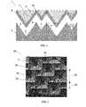
- FIG. 1Aillustrates a partial view of a re-usable mono-crystalline silicon template with hexagonal-prism posts according to the U.S. Patent Pub. No. 2008/0264477A1.
- FIG. 1Billustrates a partial view of a 3D thin-film, hexagonal-honeycomb-prism substrate with rear/bottom base silicon layer after release from the reusable template according to the U.S. Patent Pub. No. 2008/0264477A1.
- the above referenced three-dimensional thin film solar cell templates, substrates, and cellsprovide cost, performance, and mechanical strength advantages compared to traditional flat solar cells with a similar amount of silicon because 3-D TFSC have superior mechanical strength, better light trapping, and lower cell processing costs because of their self-aligned nature.
- a honeycomb 3-D TFSSmay provide a desirable mechanical rigidity and strength.
- the trenches among the neighboring hexagonal pillars on the templateneed to be filled by epitaxial silicon growth and the substrate formed by the filled layer needs to be released from the template. These processes are often costly and difficult. Design and process improvements need to be made in making the relatively high aspect ratios trenches, epitaxial filling of the trenches and releasing a TFSS from the trenches.
- flat thin film solar cellsoften require surface texturing to reduce reflectance losses which requires a minimum film thickness of preferably tens of microns (e.g., >30 ⁇ m) to avoid texturing etch-induced punch-through pinholes.
- flat thin-film silicon substratesmay have reduced mean optical path length which reduces IR absorption and results in reduced cell quantum efficiency.
- flat thin-film crystalline silicon substratesmay have poor mechanical strength for cell and module processing needs. Micro cracking defects at substrate edges and pinholes defects within the substrate could cause cracking initiations and these cracks propagate easily along the crystallographic directions.
- a needhas arisen for fabrication process improvements and manufacturing costs reductions for forming a three-dimensional thin-film solar cell (3-D TFSC).
- a three-dimensional thin-film solar cellis provided which substantially eliminates or reduces disadvantages and problems associated with previously developed 3-D TFSC.
- an inverted pyramidal three-dimensional solar cellcomprising a semiconductor substrate with an inverted pyramidal cavity, emitter metallization regions on ridges on the surface of the semiconductor substrate defining an opening of the inverted pyramidal cavity, and base metallization regions on a region forming the apex of the inverted pyramidal cavity.
- fabrication methods for forming a three-dimensional thin-film solar cell from an inverted pyramidal three-dimensional thin-film silicon substratecomprises doping ridges on the surface of the semiconductor substrate defining an opening of an inverted pyramidal cavity to form an emitter region and doping a region forming the apex of the inverted pyramidal cavity to form a base region.
- Adding a surface passivation layer to the surface of the substrateSelectively etching the passivation layer from the emitter region and base region. Then concurrently metallizing the emitter region and base region.
- a technical advantage of the simplified fabrication processes and higher gas-to-silicon conversion ratio of epitaxial growth provided when using a template having inverted pyramidal cavitiesis an inverted pyramidal cavity based 3-D TFSS provides improved mechanical rigidity and strength.
- the strength of the templatemay be adjusted according to the arrays and staggered patterns of inverted pyramidal cavities provided.
- a technical advantage of the present disclosureis innovative solar cell designs and technologies based on the use of self-supporting, free-standing, three-dimensional (3D) silicon thin films.
- the 3-D TFSCs describedmay be made to be relatively rigid, semi-rigid, or flexible depending on the structural design parameters of the cell substrate. Given an equal amount of silicon usage, the 3-D TFSS disclosed provides advantages over substrates made of flat thin-film (TF) crystalline silicon such as the following:
- Three-dimensional thin-film solar cells discloseddo not require a minimum film thickness
- Three-dimensional thin-film solar cells disclosedare mechanically robust because of their unique 3D structure, providing enhanced mechanical strength and handle-ability.
- the semiconductor templatesconsist of known crystallographic silicon planes, i.e., the (111) and (100) planes and the epitaxial silicon layer grown from these two silicon planes yields better quality than from DRIE etched silicon 3-D surfaces
- the large cavity opening angle (70.6°) of the disclosed silicon template formed by the cavity sidewall (111) planesis much wider than that may be etched from using deep reactive ion etch (DRIE) silicon etch. Therefore, the porous silicon formation, epitaxial silicon growth, and releasing of 3-D TFSS are more practical and cost efficient than a DRIE etched template.
- DRIEdeep reactive ion etch
- FIG. 1Ashows a prior art mono-crystalline silicon template
- FIG. 1Bshows a prior art three-dimensional thin-film substrate after release from the template in FIG. 1A ;
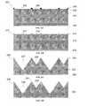
- FIG. 2illustrates a cross-sectional drawing of an inverted pyramidal template and a released corresponding three-dimensional thin-film silicon substrate
- FIG. 3is an image of a fabricated inverted pyramidal silicon template
- FIGS. 4A , 4 B, and 4 Care images of a fabricated three-dimensional thin-film silicon substrate
- FIG. 5is a process flow depicting major fabrication process steps for manufacturing an inverted pyramidal silicon template and three-dimensional thin-film silicon substrate;
- FIGS. 6A through 6Gillustrates a process flow for manufacturing an inverted pyramidal silicon template and a three-dimensional thin-film silicon substrate
- FIG. 7illustrates an array inverted pyramidal pattern on a semiconductor template
- FIGS. 8A through 8Dillustrate alternative staggered inverted pyramidal layout patterns on a semiconductor template
- FIG. 9is a process flow depicting major fabrication process steps for manufacturing a three-dimensional thin-film solar cell.
- FIGS. 10A through 10Dillustrate a process flow for manufacturing a three-dimensional thin-film solar cell.
- FIG. 1Aillustrates a partial view of a re-usable mono-crystalline silicon template with hexagonal-prism posts disclosed in U.S. Pat. Pub. No. 2008/0264477A1.
- the hexagonal pillarsare etched by deep-reactive ion etching (DRIE) with photolithographically patterned photoresist as the hard masking layer.
- DRIEdeep-reactive ion etching
- the DRIE etchingprovides well defined high-aspect ratio gaps between the pillars, however the narrow gaps are difficult to fill by the epitaxial silicon growth and it is difficult to release the epitaxial layer from such a template.
- FIG. 1Billustrates a partial view of a 3D thin-film hexagonal-honeycomb-prism substrate with a rear/bottom base silicon layer after release from a reusable template disclosed in U.S. Pat. Pub. No. 2008/0264477A1.
- FIG. 2illustrates a cross-sectional drawing of an inverted pyramidal semiconductor template and a corresponding released three-dimensional thin-film semiconductor substrate.
- Inverted pyramidal template 2is used to form corresponding released 3-D TFSS 8 .
- the inverted pyramidal templateconsists of large inverted pyramidal cavities 3 and small inverted pyramidal cavities 4 .
- Large inverted pyramidal cavity 3 and small inverted pyramidal cavity 4which are defined by walls, such as wall 5 aligned along a (111) plane of inverted pyramidal template 2 .
- Top surface 6is aligned along a (100) plane of inverted pyramidal template 2 .
- the inverted pyramid-shape cavitiesmay be chemically etched by anisotropic silicon etchant and the angle between a sidewall (such as wall 5 ) and a top lateral plane (such as top surface 6 ), is about 54.7° (angle 7 )—which is the defined angle between two (111) and (100) silicon crystallographic planes.
- Shown, small inverted pyramidal cavities 4have an apex defined by walls aligned along the (111) crystallographic planes giving the apex, or tip, of the inverted pyramid an angle of 70.6°.
- Large inverted pyramidal cavities 3have a flat apex, or flat tip, aligned along the (100) crystallographic plane.
- a semiconductor template of the disclosed subject mattermay employ various apex styles dependent on shape of the 3-D TFSS desired.
- Released 3-D TFSS 8has a bottom surface profile conformal to the top of inverted pyramidal template 2 .
- Wall 9defines inverted pyramidal cavity 11 on released 3-D TFSS 8 and surface ridge 10 defines the base opening of inverted pyramidal cavity 11 .
- FIG. 3presents a top Scanning Electron Microscope (SEM) partial view of a fabricated inverted pyramidal silicon template.
- Structured silicon template 20consists of anisotropically etched large pyramid cavity 21 and small pyramid cavity 24 .
- the top opening size 22 of the large cavitiesis in the range of 10 um to 1 mm and the top opening size 25 of the small cavities is a partial of 22 .
- the opening size of the large cavities, 22is about 300 um and opening size of the small cavities, 25 , is about 150 um.
- the depth of the small cavitiesis about 110 um and the depth of the large cavities is about 200 um.
- Top cavity surface 26 and bottom cavity surface 28are aligned along (100) silicon crystallographic planes and sidewalls 29 of the cavities are aligned along (111) silicon crystallographic planes.
- Small pyramid cavity 24has a pointed cavity apex/bottom which occurs at the intersection of four (111) sidewalls.
- Large pyramid cavity bottom 28has a flat cavity bottom/apex the size of which may be in the range of 0 to 100 um.
- top cavity surface 26is the ridge defining the opening between inverted pyramidal cavities. Top cavity surface 26 is preferably narrow and less than 10 um wide.
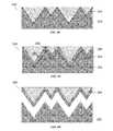
- FIG. 4Apresents a SEM partial view 40 of an embodiment of a fabricated three-dimensional thin-film silicon substrate from a tilted top perspective.
- the 3-D TFSSconsists of a staggered pattern of large cavities, 42 , and small cavities, 44 .
- crystallographic facetingoccurs and results in a structure quite different from the inverted pyramidal cavities on the semiconductor template from which the 3-D TFSS was made in accordance with the disclosed subject matter.
- ridge 46 between the cavities and defining a base opening of large cavity 42is wider on its top side due to epitaxial overgrowth on the top surfaces aligned along the (100) crystallographic plane of a semiconductor template.
- the degree or amount of the shape changedepends on the overall epitaxial silicon thickness. A thicker epitaxial thickness results in more shape change from the original silicon template structure from which 3-D TFSS was made. These shape and geometrical changes improve the mechanical strength of the 3-D TFSS and make the light trapping more effective.
- FIG. 4Bpresents a SEM partial view 60 of an embodiment of a fabricated 3-D TFSS from a tilted bottom perspective.
- the shown 3-D TFSS backsideis the reverse of the silicon template structure from which 3-D TFSS was made, which consisted of inverted pyramidal cavities forming large pyramid 62 and small pyramid 64 and ridges 66 defining the base openings of the inverted pyramidal cavities on the 3-D TFSS.
- FIG. 4Cpresents a SEM partial view 80 of an embodiment of a fabricated 3-D TFSS from a cross-sectional perspective.
- the thickness of the top ridge 82 , sidewall 84 and bottom 86may be different and could be purposefully tuned to achieve optimum mechanical, optical and electrical performances.
- a 3-D TFSC fabrication process in accordance with the disclosed subject mattermay comprise the following major steps:
- Template fabrication3-D inverted pyramidal patterns/structures are etched from a silicon wafer front surface and into the bulk silicon to form a silicon template.
- the structured silicon templateis then used in the formation of a 3-D TFSS.
- the templatemay be capable of being used numerous times to fabricate numerous 3-D TFSS before being reconditioned or recycled.
- the templatemay be reused for as long as it remains relatively free of dislocations and/or for as long as it maintains an acceptable pyramid pattern having a pyramidal size and sidewall surface conditions within acceptable control limits (e.g. as gauged by in-line metrology);
- the 3-D TFSSis optionally doped to form emitter and base regions if the doping is not conducted prior to the epitaxial layer release. Then a surface passivation layer and an antireflection layer are deposited, optional contact openings are formed, and metallization steps are conducted to form a 3-D TFSC; and
- the fabricated 3-D TFSCmay then optionally be mechanically reinforced, interconnected, encapsulated and mounted in the panels.
- FIG. 5is an embodiment of a process flow depicting major fabrication process steps for manufacturing an inverted pyramidal silicon template and three-dimensional thin-film silicon substrate.
- the silicon template making processstarts with step 105 beginning with a mono-crystalline (100) silicon wafer.
- the starting wafermay be in circular or square shapes.
- Step 110involves forming a thin hard masking layer on the exposed wafer surfaces.
- the hard masking layeris used to mask the silicon surface areas that do not need to be etched in the later steps—the surface areas that will become the top surface of the template.
- the proper hard masking layerincludes, but is not limited to, thermally grown silicon oxide and low-pressure vapor phase deposited (LPCVD) silicon nitride.
- LPCVDlow-pressure vapor phase deposited
- Step 115involves a photolithography step, which consists of photoresist coating, baking, UV light exposure over a photomask, post baking, photoresist developing, wafer cleaning and drying. After this step, the pattern on the photomask depicting an array or a staggered pattern of inverted pyramidal base openings, will be transferred to the photoresist layer.
- the patterned photoresist layeris used as a soft masking layer for the hard masking layer etching of step 120 .
- Step 120involves further transferring the photoresist pattern to the hard masking layer layered underneath by chemical etching, such as etching a thin silicon oxide layer with buffered HF solution.
- step 125the remaining soft masking layer, i.e. the photoresist layer, is removed and the wafer is cleaned.
- photoresist removal processinclude wet methods, such as using acetone or piranha solution (a mixture of sulfuric acid and hydrogen peroxide), or dry methods such as oxygen plasma ashing.
- step 130the wafers are batch loaded in an anisotropic silicon wet etchant such as KOH solution.
- the typical etch temperatureis in the range of 50° C. to 80° C. and etch rate is about 0.2 um/min to 1 um/min.
- TMAHtetramethylammonium hydroxide
- the KOH or TMAH silicon etch ratedepends upon the orientations to crystalline silicon planes.
- the (111) family of crystallographic planesare etched at a very slow rate and are normally “stop” planes for the anisotropic etching of a (100) silicon wafer with patterned hard mask.
- the intersection of two (111) planes or a (111) plane with a bottom (100) planeproduce anisotropic etching structures for (100) silicon wafers after a time-controlled etch. Examples of these structures include V-grooves and pyramidal cavities with sharp tip cavity bottom (where (111) planes meet) or a small flat cavity bottom (a remaining (100) plane).
- the template KOH etching processis more convenient to control and has a low manufacturing cost compared to other silicon etching methods, such as RIE dry etching;
- the (111) plane dominant 3-D structureprovides good porous silicon forming uniformity and epitaxial silicon quality due to the (111) plane sidewall smoothness and predictable and repeatable epitaxial growth rates;
- the dimensions, shape, and profiles of the inverted pyramidal structure on the templatemay be maintained conveniently and restored easily by a short KOH etching if needed after multiple template reuse cycles.
- step 135 of FIG. 5the remaining hard masking layer is removed, by HF solution in the case the hard masking layer is silicon dioxide.
- the wafermay be cleaned in standard SC1 (mixture of NH 4 OH and H 2 O 2 ) and SC2 (mixture of HCL and H 2 O 2 ) wafer wet cleaning solutions followed by a thorough deionized wafer rinsing and hot N 2 drying.
- SC1mixture of NH 4 OH and H 2 O 2
- SC2mixture of HCL and H 2 O 2
- Step 140 of FIG. 5marks the beginning of a silicon template re-use cycle.
- a porous silicon layeris formed by electrochemical HF etching on the silicon template front surfaces.
- the porous silicon layeris to be used as a sacrificial layer for epitaxial silicon layer release.
- the porous silicon layerpreferably consists of two thin layers with different porosities.
- the first thin porous silicon layeris a top layer and is formed first from the bulk silicon wafer.
- the first thin layerpreferably has a lower porosity of 10% ⁇ 35%.
- the second thin porous silicon layeris directly grown from the bulk silicon and is underneath the first thin layer of porous silicon.
- the 2 nd thin porous silicon layerpreferably has a higher porosity in the range of 40% ⁇ 80%.
- the top porous silicon layeris used as a crystalline seed layer for high quality epitaxial silicon growth and the bottom underneath higher porosity porous silicon layer is used for facilitating TFSS release due to its less dense physical connections between the epitaxial and bulk silicon interfaces and its weak mechanical strength.
- a single porous silicon layer with a progressively increased or graded porosity from top to bottommay also be used.
- the top portion of the porous silicon layerhas a low porosity of 10% to 35% and the lower portion of the porous silicon layer has a high porosity of 40% to 80%.
- the wafermay be baked in a high temperature (at 950° C.
- a mono-crystalline silicon epitaxial layeris deposited on the front side only.
- the bulk base of the epitaxial layeris p-type, boron (B 2 H 6 ) doped.
- the thickness of the epitaxial layeris preferably in the range of 5 um to 60 um.
- an encompassing border trenchmay be made on the peripheral of the active wafer area to facilitate the release of the TFSS.
- the encompassing trenchesmay be formed by controlled laser cutting and their depths are preferably in the range of 5 um to 100 um.
- the trenchesdefine the boundary of the 3-D TFSS to be released and allow initiation of the release from the trenched region.
- the remaining epitaxial silicon layermay be removed by mechanical grinding or polishing of the template edges.
- the epitaxial layer of siliconis released and separated from the silicon template.
- the released epitaxial silicon layeris referred to as a 3-D thin film silicon substrate (3-D TFSS).
- the 3-D TFSSmay be released in an ultrasonic DI-water bath. Or in another release method, the 3-D TFSS may be released by direct pulling with wafer backside and top epitaxial vacuum chucked. In another release method, the epitaxial layer is released by direct pulling with wafer backside and top epitaxial vacuum chucked. Using this method the porous silicon layer may be fully or partially fractured.
- the chucksmay use either electrostatic or vacuum chucking to secure the wafer. The wafer is first placed on bottom wafer chuck with TFSS substrate facing upwards. A bottom chuck secures the template side of wafer, and the top wafer chuck is gently lowered and secures TFSS substrate side of the wafer. The activated pulling mechanism lifts top chuck upwards, and the movement may be guided evenly by slider rails.
- step 170the released 3-D TFSS backside surface is cleaned by short silicon etching using KOH or TMAH solutions to remove the silicon debris and fully or partially remove the quasi-mono-crystalline silicon (QMS) layer.
- the templateis cleaned in step 175 by using diluted HF and diluted wet silicon etch solution, such as TMAH and/or KOH to remove the remaining porous silicon layers and silicon particles.
- the templateis further cleaned by conventional silicon wafer cleaning methods, such as SC1 and SC2 wet cleaning to removal possible organic and metallic contaminations.
- SC1 and SC2 wet cleaningto removal possible organic and metallic contaminations.
- FIGS. 6A through 6Ddepict cross-sectional drawings illustrating a process flow for manufacturing an inverted pyramidal silicon template.
- FIG. 6Aillustrates mono-crystalline (100) silicon wafer 201 after a hard mask deposition and soft mask patterning.
- the thickness of silicon wafer 201is in the range of 0.5 mm to 2 mm.
- the disclosed template forming processmay be applied to a polished or non-polished surface. Alternatively, silicon wafers with square or quasi-square shapes may also be used.
- Front hard mask layer 202 and backside hard mask layer 203are thermally grown silicon oxide layers having a thickness in the range of 0.5 um to 1.5 um. The oxide on the wafer edge is not shown.
- Photolithographic defined or screen-printed photoresist pattern 204is applied on the front wafer surface.
- the photolithography processincludes photoresist coating, baking, exposure, developing and post baking.
- the photoresist patternconsists of staggered pattern of large inverted pyramidal base opening 205 and small inverted pyramidal base opening 206 .
- the photoresist patternmay also be an array of equally sized inverted pyramidal base openings.
- the inverted pyramidal base opening patternsshould be precisely aligned to the wafer ⁇ 100> direction on the front surface.
- FIG. 6Billustrates wafer 212 after the inverted pyramidal base opening pattern is transferred to the hard masking layer, front oxide layer 214 .
- the pattern transferring from the photoresist layer to the oxide layeris achieved by controlled oxide etching in a buffered HF solution. During HF wet etching, backside and edge oxide layer 216 is protected and keeps an original thickness.
- the oxide pattern on the front side of wafer 212then consists of a staggered pattern of large inverted pyramidal base opening 217 and small inverted pyramidal base opening 218 that are aligned to the ⁇ 100> crystallographic directions on the front lateral plane. After the pattern transfer, the remaining photoresist layer is removed by wet or dry photoresist removal methods. Therefore, the photoresist layer is not shown in FIG. 6B .
- FIG. 6Cillustrates wafer 220 after a silicon anisotropic etching step.
- Large inverted pyramidal cavity 227 and small inverted pyramidal cavity 228are formed after a timed-controlled silicon etch in a KOH or TMAH solution.
- the etching temperatureis preferably in the range of 50° C. to 80° C.
- the KOH etchmay be timely controlled so that a certain inverted pyramidal cavity depth may be reached.
- the KOH etchingmay be self-terminated when the (111) walls forming the inverted pyramidal cavity meet at the cavity bottom/apex.
- remaining oxide layers 224 and 226are thinner than before the etching because the oxide is also etched in the KOH or TMAH solution, but with a much slower etch rate than the silicon etch.
- FIG. 6Dillustrates inverted pyramidal silicon template 232 after removing the remaining oxide layer in a diluted HF solution followed by standard wafer cleaning in SC2 and SC2, DI water rinsing, and N 2 drying.
- the width of the ridges forming the base openings of the inverted pyramidal cavities, 234is in the range of 0 to 20 um.
- the templatenow comprises a staggered pattern made of large inverted pyramidal cavity 236 and an adjacent small inverted pyramidal cavity 238 .
- the angle between the cavity sidewalls and top surface ridges aligned along the (100) crystallographic plane, the lateral plane,is 54.7°.
- FIGS. 6E through 6Gdepict cross-sectional drawings illustrating a process flow for manufacturing a 3-D TFSS using an inverted pyramidal silicon template.
- porous silicon layer 244is formed by electrochemical HF etching on the front surface of silicon template 242 .
- the porous siliconis used as a sacrificial layer and may consist of two thin layers with different porosities.
- the first thin porous silicon layeris on the top and is formed first from silicon wafer 242 .
- the first thin layerpreferably has a lower porosity of 10% ⁇ 35%.
- the second thin porous silicon layeris formed directly from silicon wafer 242 and is underneath the first thin layer of porous silicon.
- the second thin porous silicon layerpreferably has a higher porosity in the range of 40% ⁇ 80%.
- the lower porosity porous silicon layer on topis used as a crystalline seed layer for high quality epitaxial silicon growth and the underneath higher porosity porous silicon layer is used for facilitating TFSS releasing due to its less density physical connections between the epitaxial and bulk silicon interfaces and its weak mechanical strength.
- a single porosity release layer with a progressively increased or graded porosity from top to bottommay also be used.
- the top portion of the porous silicon layerhas a low porosity of 10% to 35% and the lower portion of the porous silicon layer has a high porosity of 40% to 80%.
- FIG. 6Fillustrates silicon template 252 after a thin layer of epitaxial silicon layer growth.
- mono-crystalline silicon epitaxial layer 256is deposited on porous silicon layer 254 located on the front side of silicon template 252 .
- Mono-crystalline silicon epitaxial layer 256may p-type, boron (B 2 H 6 ) doped during the growth.
- the thickness of the epitaxial layeris preferably in the range of 5 um to 60 um. It is known that crystallographic orientation is one of the factors that affect the epitaxial growth rate.
- the epitaxial growth rate on the (100) planeis faster than on the (111) plane.
- the growth rate differencecould be as large as 20%. Since the template ridge top surface is a (100) plane and the pyramid cavity sidewalls are (111) planes, the epitaxial silicon layer thickness at the top ridge region 258 is generally thicker than the sidewall regions 259 .
- the top portions (forming the base openings of the inverted pyramidal cavities) of the epitaxial layer of the pyramid structureare thicker than the bottom portions (forming the walls defining the inverted pyramidal cavities).
- This gas transportation limited growth rate differentialcould be enhanced by tuning gas pressures, flow rates, chamber sizes, and other physical parameters of the epitaxial process.
- the higher epitaxial growth rates at top portions of the pyramid cavitiesalso generate faceting around the ridge areas. The faceting effect may changes the square opening patterns into polygon opening patterns as shown in FIG. 4A .
- the combined thickness increases (overgrowth) and shape changesgenerate a unique structure that resembles a prism-grid structure.
- the 3-D TFSS of the present disclosureprovides the following unique features:
- the thickness increase and resulting polygon shape formed on the top surface of a 3-D TFSSprovides significant enhancement to its mechanical rigidity and strength.
- the template top ridgescorrespond to the V-grooves of 3-D TFSS when viewed from the backside. When a 3-D TFSS is under a bending load, the V-groove areas have higher stress concentration than the sidewall areas. The increased thickness and the polygon shape at the top portion therefore enhance the mechanical handle-ability of the 3-D TFSS;
- the top surface profile at the ridgesmay be sharpener than the original template ridge surface profile.
- the top surface ridge sharpening effectmay increase the optical trapping and/or electrical efficiencies;
- the TFSS surfacesare made of crystallographic planes.
- a diluted anisotropic etchantsuch as KOH
- the top surfacescan be further sharpened to increase the optical and electrical efficiencies of the resulting solar cells.
- the disclosed subject mattertakes advantage of the higher etch rates of convex crystallographic edges than concave edges in anisotropic silicon etching.
- FIG. 6Gillustrates 3-D TFSS 264 that is released from silicon template 262 .
- an encompassing border trenchmay be made on the peripheral of the active wafer area to facilitate the release.
- the encompassing trenchesare formed by controlled laser cutting and their depths are preferably in the range of 5 um to 100 um.
- the trenchesdefine the boundary of the 3-D TFSS to be released and allow initiation of the release from the trenched region.
- the thin epitaxial layer on the template edgecould be removed first by mechanical grinding and then defining the shape of the 3-D TFSS by laser trimming after it has been released from the template.
- the released epitaxial layer, referred to as 3-D TFSS 264is physically separate from silicon template 262 .
- the epitaxial layer release methods disclosed in U.S. patent application Ser. No. 12/473,811 entitled, SUBSTRATE RELEASE METHODS AND APPARATUSare hereby incorporated by reference.
- the epitaxial layermay be released in an ultrasonic DI-water bath.
- the epitaxial layeris released by direct pulling with wafer backside and top epitaxial vacuum chucked.
- the epitaxial layeris released by direct pulling with wafer backside and top epitaxial vacuum chucked.
- the porous silicon layermay be fully or partially fractured.
- the chucksmay use either electrostatic or vacuum chucking to secure the wafer.
- the waferis first placed on bottom wafer chuck with TFSS substrate facing upwards.
- a bottom chucksecures the template side of wafer, and the top wafer chuck is gently lowered and secures TFSS substrate side of the wafer.
- the activated pulling mechanismlifts top chuck upwards, and the movement may be guided evenly by slider rails.
- the templateis cleaned by using diluted HF and diluted wet silicon etch solution, such as TMAH and/or KOH to remove the remaining porous silicon layers and silicon particles.
- TMAH and/or KOHdiluted wet silicon etch solution
- the templatemay then be further cleaned by conventional silicon wafer cleaning methods, such as SC1 and/or SC2 wet cleaning to removal possible organic and metallic contaminations.
- SC1 and/or SC2 wet cleaningto removal possible organic and metallic contaminations.
- the templateis ready for another re-use cycle.
- the released TFSS backside surfaceis cleaned by short silicon etching using KOH or TMAH solutions to remove the silicon debris and fully or partially remove the QMS layer.
- inverted pyramidal cavity structuresinstead of non-inverted pyramidal pillar structures.
- the corners/edges where (111) planes meetare “concave”.
- the (111) planesform the sidewalls of pyramidal cavities.
- there have been reported “convex” caseswhere the (111) planes form the sidewalls of pyramidal pillars.
- An inverted-pyramid cavity structure with “concave” cornersis preferable over a non-inverted pyramid pillar structure with “convex” corners because of the following reasons:
- inverted pyramidal cavitieshave only (111) planes for sidewall and (100) planes for top surface, an epitaxial growth from these crystallographic surfaces have better geometry and process control than the non-inverted-pyramidal pillar case;
- the silicon templatecan be conveniently cleaned and re-conditioned in a short time by anisotropic etching after each re-use cycle or once every several reuse cycles.
- the mechanical handle-ability of the 3-D TFSSis another key factor in the template structure design.
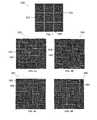
- FIG. 7illustrates a template having an array, or non-staggered, pattern inverted pyramidal cavities.
- Pyramidal cavities 302all have the same base opening size and thus the same cavity depth, and are arranged in an array.
- Ridges 304form lateral rows and columns between the inverted pyramidal cavities. These ridges may be referred to as frames, grids, space lines, or ridge lines. Ridges 304 are aligned to the (100) crystallographic direction of the template. The straight long ridges between the cavities on the template will be transferred to the backside of a corresponding 3-D TFSS made in accordance with the disclosed subject matter in long V-groove shapes. The V-grooves on the 3-D TFSS are aligned to the (100) crystallographic directions.
- FIG. 8A through 8Dillustrate four examples of template layout patterns of staggered inverted pyramidal cavity designs.
- Staggered patternsavoid long V-groove on the 3-D TFSS because staggered patterns limit the length of the ridges forming the base openings of the inverted pyramidal cavities (in both rows and columns as shown form a top view of the template).
- the staggered pattern designs of the present disclosureare not limited to the described embodiments but instead include any staggered pattern of inverted pyramidal cavities.
- FIG. 8Ashows a staggered inverted pyramidal cavity layout pattern that consists of two cavity sizes.
- Small cavity 324has a base opening half the size of the base opening of large cavity 322 .
- the V-groove length on the corresponding 3-D TFSSwill be about 1.5 times as long as the length of one side of the base opening of large cavity 322 .
- each ridge on template 320 and each V-groove on the formed 3-D TFSSis intersected at twice (each at one third the length of the ridge or V-groove) by neighboring perpendicular ridges or V-grooves.
- the intersection of V-grooves of a 3-D TFSS made with this staggered patternare uniformly spread giving this staggered pattern good mechanical handle-ability and uniform mechanical strength across its lateral plane.
- FIG. 8Bpresents another alternative staggered inverted pyramidal cavity layout pattern that consists of two cavity sizes.
- Small cavity 344has a base opening that is a fraction of the base opening of large cavity 342 . Shown, the ratio between the two cavity sizes is between 1 and 2.
- This cavity layout patternis a general pattern of the layout shown in FIG. 8A . In this design, the V-groove length on the formed 3-D TFSS is about 1 to 2 times of the cavity length.
- the inverted pyramidal cavity layoutsmay include different inverted pyramidal cavity shapes (such as rectangular) and staggered inverted pyramidal cavities with more than two sizes.
- FIG. 8Cpresents an alternative staggered inverted pyramidal cavity layout that consists of rectangular cavity 362 and square cavity 364 .
- Square cavity 364has a base opening size equal to the width of the base opening of rectangular cavity 362 .
- Each square cavityis surrounded by two pairs of perpendicularly arranged rectangular cavities.
- the length of the V-grooves on the formed 3-D TFSSwill be about the length of the base opening of rectangular cavity 362 plus twice the width of rectangular cavity 362 .
- FIG. 8Dpresents yet another alternative staggered inverted pyramidal cavity layout that consists of one size of inverted pyramidal cavities.
- Each rectangular cavity 382has the same size and is arranged in a staggered perpendicular format.
- the length of the V-grooves on the 3-D TFSSwill be about the length of the base opening of rectangular cavity 382 plus the width of rectangular cavity 382 on the template.
- FIG. 9is a process flow depicting major fabrication process steps of an exemplary method for making a 3-D TFSC using the released 3-D TFSS, in a block diagram 400 .
- the 3-D TFSC fabrication processstarts in Step 405 with a p-type silicon 3-D thin film substrate (3-D TFSS) having inverted pyramidal ridges on a top surface plane and inverted pyramidal apex regions on a bottom surface.
- Step 410involves selectively coating the top ridge areas of the 3-D TFSS with an n-type (such as phosphorus) liquid dopant. Viewed from a top perspective, the coated areas form long lines that are connected at cell edges to form fingers and busbars patterns as in regular flat silicon based solar cells.
- n-typesuch as phosphorus
- the doped fingers and busbars lines on the top ridge areasmay not be straight lines if the inverted pyramidal cavity pattern layout is staggered.
- the selective liquid dopant coatingmay be done by aligned screen printing, roller coating, or direct inkjet dispense. After the coating, the coated layer is dried and cured (e.g., by thermal curing at 250° C. to 400° C. or UV irradiation).
- Step 415involves selectively coating the bottom side of the 3-D TFSS with p-type (such as boron) liquid dopant.
- the liquid dopantis selectively coated to the inverted pyramidal apex regions on the bottom surface of the 3-D TFSS by aligned or self-aligned roller coating, screen printing, or dip-coating methods. After the coating, the coated layer is dried and cured (e.g., by thermal curing at 250° C. to 400° C. or UV irradiation).
- Step 420involves forming n++ selective emitter and p++ base diffusion contact regions by thermal annealing that may be done in a diffusion furnace at 800° C. to 950° C., where the emitter and base are concurrently formed.
- Step 425involves a surface passivation process. In one embodiment, a thermal oxide layer of 10 to 200 nanometers is grown at 800° C.
- Step 430involves making local openings on the emitter and base contact regions by selective passivation layer chemical etching, such as by applying HF-based etchant by inkjet dispensing. The contact openings are made smaller than the dopant diffused areas to avoid shunting after metallization.
- Step 435involves self-aligned metallization.
- the emitter and base metallized regionsare concurrently formed using selective electroplating and/or electroless plating to form single or multilayer high-conductivity metallized regions of silver, aluminum, nickel, titanium, cobalt, or tantalum.
- the plated metal stackmay include a thin (50 to 500 nanometers) barrier and adhesion layer (made of nickel) followed by a relatively thick (2 to 15 microns) layer of high-conductivity metal (silver, copper, or aluminum).
- the metal contactsmay be formed by the aligned inkjet dispense or screen printing of metal particles, such as silver nano-particles in a liquid solution or paste.
- Step 445involves mounting the 3-D thin film solar cell (3-D TFSC) onto a plate with a metal surface or metal lines to interconnect the base contacts.
- the metal platepreferably has a reflective surface to serve as a rear reflection mirror.
- the mountingcould direct metal-to-metal fusion or with a highly conductive adhesive.
- Step 450involves packaging the fabricated solar cell into a solar module assembly. In this manufacturing module, the emitter and base metal contacts are interconnected among the solar cells to form the power output connections of a solar panel.
- FIG. 10A through 10Dillustrate partial cross-sectional views of a process flow for manufacturing a three-dimensional thin-film solar cell according to the process steps of FIG. 9 .
- FIG. 10Aillustrates 3-D TFSS 512 after the selective emitter 514 and base 516 coating steps.
- the liquid dopantssuch as phosphorus-contained liquid for emitter and boron-contained liquid for base, are dried and cured after their selective coatings.
- FIG. 10Billustrates 3-D TFSS 522 after the selective emitter 524 and base 526 diffusion and passivation layer 528 coating steps.
- the emitter and base diffusion regionsare concurrently formed in a diffusion furnace with a controlled time and temperature.
- the actual doping profilemay be extended towards to the sidewalls near the contact regions.
- the remaining dopant material and dielectric layers formed during the diffusion processare removed.
- a passivation layeris then applied on both the front and base surfaces of the 3-D TFSS. Examples of the passivation layer include thermally grown silicon dioxide and PECVD silicon nitride.
- FIG. 10Cillustrates 3-D TFSS 532 after the selective emitter 534 and base 536 contact openings are formed.
- the local openings on the emitter and base contact regionsare made by selective passivation layer chemical etching, such as by applying HF-based etchant by inkjet dispensing.
- the contact openingsare made smaller than the dopant diffused areas to avoid shunting after metallization. Portions of the top and bottom surface of the 3-D TFSS remain coated with passivation layer 538 .
- FIG. 10Dillustrates a completed 3-D TFSS 542 after all the cell fabrication process disclosed in FIG. 9 .
- the emitter metal 544 and base metal 546are electroplated or electroless plated single or multilayer high-conductivity metallized regions (silver, aluminum, nickel, titanium, cobalt, or tantalum). Alternatively, the metal layer could be inkjet dispensed.
- the emitter metal contactsare formed in continuous metal lines, i.e. fingers and busbars on the 3-D TFSC top surface. However, because the base metal contacts have been formed on the inverted pyramidal apex regions on the backside of the 3-D TFSS, the base metal contacts are isolated regions.
- the front surface passivation layermay also serve as the antireflection layer given a controlled thickness.
- the 3-D TFSS after metallizationis mounted on a supporting non-metal plate 550 with continuous metal surface or patterned metal lines 552 to form the base interconnects of the 3-D TFSC. Portions of the top and bottom surface of the 3-D TFSS remain coated with passivation layer 548 .
- the 3-D TFSS and cell process flows as shown is FIGS. 5 , 6 , 9 and 10may be applied to substrate doping polarity of n-type for p-type selective emitters.
- the 3-D TFSS basecould be either n-type or p-type with corresponding emitter polarities.
Landscapes
- Engineering & Computer Science (AREA)
- Physics & Mathematics (AREA)
- Manufacturing & Machinery (AREA)
- Computer Hardware Design (AREA)
- General Physics & Mathematics (AREA)
- Condensed Matter Physics & Semiconductors (AREA)
- Plasma & Fusion (AREA)
- Microelectronics & Electronic Packaging (AREA)
- Power Engineering (AREA)
- Weting (AREA)
- Photovoltaic Devices (AREA)
- Life Sciences & Earth Sciences (AREA)
- Chemical & Material Sciences (AREA)
- Crystallography & Structural Chemistry (AREA)
- Sustainable Development (AREA)
Abstract
Description
Claims (13)
Priority Applications (2)
| Application Number | Priority Date | Filing Date | Title |
|---|---|---|---|
| US12/618,668US8294026B2 (en) | 2008-11-13 | 2009-11-13 | High-efficiency thin-film solar cells |
| US13/657,745US20130284255A1 (en) | 2008-11-13 | 2012-10-22 | High-Efficiency Thin-Film Solar Cells |
Applications Claiming Priority (2)
| Application Number | Priority Date | Filing Date | Title |
|---|---|---|---|
| US11437808P | 2008-11-13 | 2008-11-13 | |
| US12/618,668US8294026B2 (en) | 2008-11-13 | 2009-11-13 | High-efficiency thin-film solar cells |
Related Child Applications (1)
| Application Number | Title | Priority Date | Filing Date |
|---|---|---|---|
| US13/657,745ContinuationUS20130284255A1 (en) | 2008-11-13 | 2012-10-22 | High-Efficiency Thin-Film Solar Cells |
Publications (2)
| Publication Number | Publication Date |
|---|---|
| US20100175752A1 US20100175752A1 (en) | 2010-07-15 |
| US8294026B2true US8294026B2 (en) | 2012-10-23 |
Family
ID=42170752
Family Applications (6)
| Application Number | Title | Priority Date | Filing Date |
|---|---|---|---|
| US12/618,663AbandonedUS20100148319A1 (en) | 2008-11-13 | 2009-11-13 | Substrates for High-Efficiency Thin-Film Solar Cells Based on Crystalline Templates |
| US12/618,649Expired - Fee RelatedUS8168465B2 (en) | 2006-10-09 | 2009-11-13 | Three-dimensional semiconductor template for making high efficiency thin-film solar cells |
| US12/618,668Expired - Fee RelatedUS8294026B2 (en) | 2008-11-13 | 2009-11-13 | High-efficiency thin-film solar cells |
| US13/345,935Expired - Fee RelatedUS8664737B2 (en) | 2006-10-09 | 2012-01-09 | Three-dimensional semiconductor template for making high efficiency thin-film solar cells |
| US13/657,745AbandonedUS20130284255A1 (en) | 2008-11-13 | 2012-10-22 | High-Efficiency Thin-Film Solar Cells |
| US14/195,748Expired - Fee RelatedUS9590035B2 (en) | 2008-11-13 | 2014-03-03 | Three-dimensional semiconductor template for making high efficiency solar cells |
Family Applications Before (2)
| Application Number | Title | Priority Date | Filing Date |
|---|---|---|---|
| US12/618,663AbandonedUS20100148319A1 (en) | 2008-11-13 | 2009-11-13 | Substrates for High-Efficiency Thin-Film Solar Cells Based on Crystalline Templates |
| US12/618,649Expired - Fee RelatedUS8168465B2 (en) | 2006-10-09 | 2009-11-13 | Three-dimensional semiconductor template for making high efficiency thin-film solar cells |
Family Applications After (3)
| Application Number | Title | Priority Date | Filing Date |
|---|---|---|---|
| US13/345,935Expired - Fee RelatedUS8664737B2 (en) | 2006-10-09 | 2012-01-09 | Three-dimensional semiconductor template for making high efficiency thin-film solar cells |
| US13/657,745AbandonedUS20130284255A1 (en) | 2008-11-13 | 2012-10-22 | High-Efficiency Thin-Film Solar Cells |
| US14/195,748Expired - Fee RelatedUS9590035B2 (en) | 2008-11-13 | 2014-03-03 | Three-dimensional semiconductor template for making high efficiency solar cells |
Country Status (3)
| Country | Link |
|---|---|
| US (6) | US20100148319A1 (en) |
| EP (1) | EP2356675B1 (en) |
| WO (1) | WO2010057060A2 (en) |
Cited By (16)
| Publication number | Priority date | Publication date | Assignee | Title |
|---|---|---|---|---|
| US20110214368A1 (en)* | 2010-03-03 | 2011-09-08 | Haddock Robert M M | Photovoltaic module mounting assembly |
| US20110318863A1 (en)* | 2010-06-25 | 2011-12-29 | Taiwan Semiconductor Manufacturing Company, Ltd. | Photovoltaic device manufacture |
| US8637340B2 (en) | 2004-11-30 | 2014-01-28 | Solexel, Inc. | Patterning of silicon oxide layers using pulsed laser ablation |
| US9455361B2 (en) | 2013-07-22 | 2016-09-27 | Globalfoundries Inc. | Segmented thin film solar cells |
| US9590035B2 (en) | 2008-11-13 | 2017-03-07 | Solexel, Inc. | Three-dimensional semiconductor template for making high efficiency solar cells |
| US10443896B2 (en) | 2016-07-29 | 2019-10-15 | Rmh Tech Llc | Trapezoidal rib mounting bracket with flexible legs |
| US10634175B2 (en) | 2011-12-29 | 2020-04-28 | Rmh Tech Llc | Mounting device for nail strip panels |
| US10640980B2 (en) | 2016-10-31 | 2020-05-05 | Rmh Tech Llc | Metal panel electrical bonding clip |
| US10731355B2 (en) | 2011-02-25 | 2020-08-04 | Rmh Tech Llc | Mounting device for building surfaces having elongated mounting slot |
| US10903785B2 (en) | 2018-03-21 | 2021-01-26 | Rmh Tech Llc | PV module mounting assembly with clamp/standoff arrangement |
| US10948002B2 (en) | 2018-12-14 | 2021-03-16 | Rmh Tech Llc | Mounting device for nail strip panels |
| US11041310B1 (en) | 2020-03-17 | 2021-06-22 | Rmh Tech Llc | Mounting device for controlling uplift of a metal roof |
| US11352793B2 (en) | 2020-03-16 | 2022-06-07 | Rmh Tech Llc | Mounting device for a metal roof |
| US11774143B2 (en) | 2017-10-09 | 2023-10-03 | Rmh Tech Llc | Rail assembly with invertible side-mount adapter for direct and indirect mounting applications |
| US12203496B2 (en) | 2020-07-09 | 2025-01-21 | Rmh Tech Llc | Mounting system, device, and method |
| USD1075493S1 (en) | 2022-07-06 | 2025-05-20 | Rmh Tech Llc | Clamp for a photovoltaic module mounting assembly |
Families Citing this family (42)
| Publication number | Priority date | Publication date | Assignee | Title |
|---|---|---|---|---|
| US8399331B2 (en) | 2007-10-06 | 2013-03-19 | Solexel | Laser processing for high-efficiency thin crystalline silicon solar cell fabrication |
| US9508886B2 (en) | 2007-10-06 | 2016-11-29 | Solexel, Inc. | Method for making a crystalline silicon solar cell substrate utilizing flat top laser beam |
| US20090107545A1 (en) | 2006-10-09 | 2009-04-30 | Soltaix, Inc. | Template for pyramidal three-dimensional thin-film solar cell manufacturing and methods of use |
| US8193076B2 (en) | 2006-10-09 | 2012-06-05 | Solexel, Inc. | Method for releasing a thin semiconductor substrate from a reusable template |
| US9455362B2 (en) | 2007-10-06 | 2016-09-27 | Solexel, Inc. | Laser irradiation aluminum doping for monocrystalline silicon substrates |
| US8288195B2 (en)* | 2008-11-13 | 2012-10-16 | Solexel, Inc. | Method for fabricating a three-dimensional thin-film semiconductor substrate from a template |
| US8906218B2 (en) | 2010-05-05 | 2014-12-09 | Solexel, Inc. | Apparatus and methods for uniformly forming porous semiconductor on a substrate |
| US9076642B2 (en) | 2009-01-15 | 2015-07-07 | Solexel, Inc. | High-Throughput batch porous silicon manufacturing equipment design and processing methods |
| US9318644B2 (en) | 2009-05-05 | 2016-04-19 | Solexel, Inc. | Ion implantation and annealing for thin film crystalline solar cells |
| CN102763226B (en) | 2009-12-09 | 2016-01-27 | 速力斯公司 | Use high-efficiency photovoltaic back of the body contact solar cell structure and the manufacture method of thin plate semiconductor |
| US8241940B2 (en) | 2010-02-12 | 2012-08-14 | Solexel, Inc. | Double-sided reusable template for fabrication of semiconductor substrates for photovoltaic cell and microelectronics device manufacturing |
| US20110212622A1 (en)* | 2010-02-26 | 2011-09-01 | International Business Machines Corporation | Surface texturing using a low quality dielectric layer |
| JP5734734B2 (en)* | 2010-05-18 | 2015-06-17 | ローム アンド ハース エレクトロニック マテリアルズ エルエルシーRohm and Haas Electronic Materials LLC | Method for forming current tracks on a semiconductor |
| EP2577750A4 (en)* | 2010-05-27 | 2014-04-09 | Solexel Inc | LASER PROCESSING FOR MANUFACTURING THIN SILICON CRYSTALLINE HIGH EFFICIENCY SILICON CELLS |
| KR20130051013A (en) | 2010-06-09 | 2013-05-16 | 솔렉셀, 인크. | High productivity thin film deposition method and system |
| TW201200465A (en)* | 2010-06-29 | 2012-01-01 | Univ Nat Central | Nano/micro-structure and fabrication method thereof |
| EP2601687A4 (en) | 2010-08-05 | 2018-03-07 | Solexel, Inc. | Backplane reinforcement and interconnects for solar cells |
| EP2635513A4 (en)* | 2010-11-01 | 2014-04-16 | Intevac Inc | DRY ETCHING METHOD FOR FORMING SURFACE TEXTURE ON SILICON WAFER |
| US9748414B2 (en) | 2011-05-20 | 2017-08-29 | Arthur R. Zingher | Self-activated front surface bias for a solar cell |
| US20130137244A1 (en)* | 2011-05-26 | 2013-05-30 | Solexel, Inc. | Method and apparatus for reconditioning a carrier wafer for reuse |
| CN103094374B (en) | 2011-10-27 | 2016-03-09 | 清华大学 | Solar cell |
| CN103137811B (en) | 2011-12-03 | 2015-11-25 | 清华大学 | Light-emitting diode |
| CN103137812B (en) | 2011-12-03 | 2015-11-25 | 清华大学 | Light-emitting diode |
| CN103137816B (en) | 2011-12-03 | 2015-09-30 | 清华大学 | Light-emitting diode |
| US9583651B2 (en)* | 2011-12-26 | 2017-02-28 | Solexel, Inc. | Systems and methods for enhanced light trapping in solar cells |
| CN104380470B (en)* | 2012-05-18 | 2018-01-02 | 富士电机株式会社 | Semiconductor device |
| US8940580B2 (en) | 2012-06-28 | 2015-01-27 | International Business Machines Corporation | Textured multi-junction solar cell and fabrication method |
| US9105775B2 (en) | 2012-06-28 | 2015-08-11 | International Business Machines Corporation | Textured multi-junction solar cell and fabrication method |
| US9293624B2 (en)* | 2012-12-10 | 2016-03-22 | Sunpower Corporation | Methods for electroless plating of a solar cell metallization layer |
| US9831361B2 (en)* | 2012-12-14 | 2017-11-28 | Robert Bosch Gmbh | Method of fabricating nanocone texture on glass and transparent conductors |
| WO2014155833A1 (en)* | 2013-03-28 | 2014-10-02 | 三洋電機株式会社 | Solar battery |
| US11121271B2 (en) | 2013-05-22 | 2021-09-14 | W&WSens, Devices, Inc. | Microstructure enhanced absorption photosensitive devices |
| US10468543B2 (en) | 2013-05-22 | 2019-11-05 | W&Wsens Devices, Inc. | Microstructure enhanced absorption photosensitive devices |
| US10700225B2 (en) | 2013-05-22 | 2020-06-30 | W&Wsens Devices, Inc. | Microstructure enhanced absorption photosensitive devices |
| CN105556680B (en) | 2013-05-22 | 2017-12-22 | 王士原 | Microstructure-enhanced absorption photosensitive device |
| US10446700B2 (en)* | 2013-05-22 | 2019-10-15 | W&Wsens Devices, Inc. | Microstructure enhanced absorption photosensitive devices |
| JP6356476B2 (en)* | 2014-04-28 | 2018-07-11 | 新光電気工業株式会社 | Solar cell mounting substrate and solar cell module |
| US9758261B1 (en)* | 2015-01-15 | 2017-09-12 | Solaero Technologies Corp. | Inverted metamorphic multijunction solar cell with lightweight laminate substrate |
| US20180053662A1 (en)* | 2016-08-17 | 2018-02-22 | Globalfoundries Inc. | Texturing of silicon surface with direct-self assembly patterning |
| US10424441B2 (en) | 2017-07-05 | 2019-09-24 | Honeywell International Inc. | Ultra-high charge density electrets and method of making same |
| CN111217320B (en)* | 2020-01-15 | 2023-08-04 | 中国科学院高能物理研究所 | Method for growing cadmium sulfide nanowire array on surface of silicon wafer |
| CN114369360B (en)* | 2021-11-29 | 2023-07-25 | 南方科技大学 | A high-stability three-dimensional braided flexible electromagnetic shielding film and its preparation method |
Citations (121)
| Publication number | Priority date | Publication date | Assignee | Title |
|---|---|---|---|---|
| US4043894A (en) | 1976-05-20 | 1977-08-23 | Burroughs Corporation | Electrochemical anodization fixture for semiconductor wafers |
| US4070206A (en) | 1976-05-20 | 1978-01-24 | Rca Corporation | Polycrystalline or amorphous semiconductor photovoltaic device having improved collection efficiency |
| US4082570A (en) | 1976-02-09 | 1978-04-04 | Semicon, Inc. | High intensity solar energy converter |
| US4165252A (en) | 1976-08-30 | 1979-08-21 | Burroughs Corporation | Method for chemically treating a single side of a workpiece |
| US4249959A (en)* | 1979-11-28 | 1981-02-10 | Rca Corporation | Solar cell construction |
| US4251679A (en)* | 1979-03-16 | 1981-02-17 | E-Cel Corporation | Electromagnetic radiation transducer |
| US4348254A (en)* | 1978-12-27 | 1982-09-07 | Solarex Corporation | Method of making solar cell |
| US4361950A (en) | 1980-03-24 | 1982-12-07 | Exxon Research & Engineering Co. | Method of making solar cell with wrap-around electrode |
| US4409423A (en) | 1982-03-09 | 1983-10-11 | The United States Of America As Represented By The Secretary Of The Air Force | Hole matrix vertical junction solar cell |
| US4427839A (en) | 1981-11-09 | 1984-01-24 | General Electric Company | Faceted low absorptance solar cell |
| US4430519A (en)* | 1982-05-28 | 1984-02-07 | Amp Incorporated | Electron beam welded photovoltaic cell interconnections |
| US4461922A (en) | 1983-02-14 | 1984-07-24 | Atlantic Richfield Company | Solar cell module |
| US4479847A (en) | 1981-12-30 | 1984-10-30 | California Institute Of Technology | Equilibrium crystal growth from substrate confined liquid |
| US4626613A (en) | 1983-12-23 | 1986-12-02 | Unisearch Limited | Laser grooved solar cell |
| US4672023A (en) | 1985-10-21 | 1987-06-09 | Avantek, Inc. | Method for planarizing wafers |
| US4922277A (en) | 1988-11-28 | 1990-05-01 | The United States Of America As Represented By The Secretary Of The Air Force | Silicon wafer photoresist developer |
| US5024953A (en) | 1988-03-22 | 1991-06-18 | Hitachi, Ltd. | Method for producing opto-electric transducing element |
| US5073230A (en) | 1990-04-17 | 1991-12-17 | Arizona Board Of Regents Acting On Behalf Of Arizona State University | Means and methods of lifting and relocating an epitaxial device layer |
| US5112453A (en) | 1990-10-31 | 1992-05-12 | Behr Omri M | Method and apparatus for producing etched plates for graphic printing |
| US5208068A (en) | 1989-04-17 | 1993-05-04 | International Business Machines Corporation | Lamination method for coating the sidewall or filling a cavity in a substrate |
| US5248621A (en) | 1990-10-23 | 1993-09-28 | Canon Kabushiki Kaisha | Method for producing solar cell devices of crystalline material |
| US5316593A (en) | 1992-11-16 | 1994-05-31 | Midwest Research Institute | Heterojunction solar cell with passivated emitter surface |
| JPH06260670A (en)* | 1993-03-05 | 1994-09-16 | Hitachi Ltd | Light confinement structure for solar cells |
| US5348618A (en) | 1989-12-07 | 1994-09-20 | The Secretary Of State For Defence In Her Britannic Majesty's Government Of The United Kingdom Of Great Britain And Northern Ireland | Method of making silicon quantum wires |
| US5397400A (en) | 1992-07-22 | 1995-03-14 | Mitsubishi Denki Kabushiki Kaisha | Thin-film solar cell |
| US5458755A (en) | 1992-11-09 | 1995-10-17 | Canon Kabushiki Kaisha | Anodization apparatus with supporting device for substrate to be treated |
| US5459099A (en) | 1990-09-28 | 1995-10-17 | The United States Of America As Represented By The Secretary Of The Navy | Method of fabricating sub-half-micron trenches and holes |
| US5494832A (en) | 1993-03-29 | 1996-02-27 | Siemens Aktiengesellschaft | Method for manufacturing a solar cell from a substrate wafer |
| US5538564A (en) | 1994-03-18 | 1996-07-23 | Regents Of The University Of California | Three dimensional amorphous silicon/microcrystalline silicon solar cells |
| US5645684A (en) | 1994-03-07 | 1997-07-08 | The Regents Of The University Of California | Multilayer high vertical aspect ratio thin film structures |
| US5660680A (en) | 1994-03-07 | 1997-08-26 | The Regents Of The University Of California | Method for fabrication of high vertical aspect ratio thin film structures |
| US5681392A (en) | 1995-12-21 | 1997-10-28 | Xerox Corporation | Fluid reservoir containing panels for reducing rate of fluid flow |
| US5704992A (en)* | 1993-07-29 | 1998-01-06 | Willeke; Gerhard | Solar cell and method for manufacturing a solar cell |
| US5882988A (en) | 1995-08-16 | 1999-03-16 | Philips Electronics North America Corporation | Semiconductor chip-making without scribing |
| US5899360A (en) | 1995-06-09 | 1999-05-04 | Colgate - Palmolive Company | Multi-chamber refillable dispenser |
| US5928438A (en) | 1995-10-05 | 1999-07-27 | Ebara Solar, Inc. | Structure and fabrication process for self-aligned locally deep-diffused emitter (SALDE) solar cell |
| US5994640A (en) | 1997-04-16 | 1999-11-30 | Eurocopter Deutschland Gmbh | Solar generator with energy damping for satellites |
| US6058945A (en) | 1996-05-28 | 2000-05-09 | Canon Kabushiki Kaisha | Cleaning methods of porous surface and semiconductor surface |
| US6091021A (en) | 1996-11-01 | 2000-07-18 | Sandia Corporation | Silicon cells made by self-aligned selective-emitter plasma-etchback process |
| US6096229A (en) | 1998-07-30 | 2000-08-01 | Lucent Technologies Inc. | Method of making alignment grooves in an optical connector support member |
| US6114046A (en) | 1997-07-24 | 2000-09-05 | Evergreen Solar, Inc. | Encapsulant material for solar cell module and laminated glass applications |
| US6127623A (en) | 1998-07-03 | 2000-10-03 | Sharp Kabushiki Kaisha | Solar cell and production process therefor |
| US6143629A (en) | 1998-09-04 | 2000-11-07 | Canon Kabushiki Kaisha | Process for producing semiconductor substrate |
| US6204443B1 (en) | 1997-06-09 | 2001-03-20 | Canon Kabushiki Kaisha | Solar cell module having a specific front side covering material and a process for the production of said solar cell module |
| US6225193B1 (en) | 1998-08-28 | 2001-05-01 | Nortel Networks Limited | Method of cleaving a semiconductor wafer including implanting and annealing resulting in exfoliation |
| US6294725B1 (en) | 2000-03-31 | 2001-09-25 | Trw Inc. | Wireless solar cell array electrical interconnection scheme |
| US6331208B1 (en) | 1998-05-15 | 2001-12-18 | Canon Kabushiki Kaisha | Process for producing solar cell, process for producing thin-film semiconductor, process for separating thin-film semiconductor, and process for forming semiconductor |
| US6399143B1 (en) | 1996-04-09 | 2002-06-04 | Delsys Pharmaceutical Corporation | Method for clamping and electrostatically coating a substrate |
| US20020079290A1 (en) | 1998-03-18 | 2002-06-27 | Konstantin Holdermann | Etching solution for wet chemical pyramidal texture etching of silicon surfaces |
| US6416647B1 (en) | 1998-04-21 | 2002-07-09 | Applied Materials, Inc. | Electro-chemical deposition cell for face-up processing of single semiconductor substrates |
| US6429037B1 (en) | 1998-06-29 | 2002-08-06 | Unisearch Limited | Self aligning method for forming a selective emitter and metallization in a solar cell |
| US6428620B1 (en) | 1997-12-26 | 2002-08-06 | Canon Kabushiki Kaisha | Substrate processing method and apparatus and SOI substrate |
| US6441297B1 (en) | 1998-03-13 | 2002-08-27 | Steffen Keller | Solar cell arrangement |
| US6448155B1 (en) | 1999-06-17 | 2002-09-10 | Canon Kabushiki Kaisha | Production method of semiconductor base material and production method of solar cell |
| US6461932B1 (en) | 1998-12-14 | 2002-10-08 | National Semiconductor Corporation | Semiconductor trench isolation process that utilizes smoothening layer |
| US20020153039A1 (en)* | 2001-04-23 | 2002-10-24 | In-Sik Moon | Solar cell and method for fabricating the same |
| US20020168592A1 (en) | 2001-04-19 | 2002-11-14 | Vezenov Dmitri V. | Method of fabricating sub-micron hemispherical and hemicylidrical structures from non-spherically shaped templates |
| US20020179140A1 (en) | 2001-05-30 | 2002-12-05 | Fumitaka Toyomura | Power converter, and photovoltaic element module and power generator using the same |
| US20030017712A1 (en) | 1997-06-30 | 2003-01-23 | Rolf Brendel | Method for producing layered structures on a substrate, substrate and semiconductor components produced according to said method |
| US20030039843A1 (en) | 1997-03-14 | 2003-02-27 | Christopher Johnson | Photoactive coating, coated article, and method of making same |
| US6534336B1 (en) | 1999-05-21 | 2003-03-18 | Canon Kabushiki Kaisha | Production method of photoelectric conversion device, and photoelectric conversion device produced by the method |
| US6551908B2 (en) | 2000-10-02 | 2003-04-22 | Canon Kabushiki Kaisha | Method for producing semiconductor thin films on moving substrates |
| US6555443B1 (en) | 1998-11-11 | 2003-04-29 | Robert Bosch Gmbh | Method for production of a thin film and a thin-film solar cell, in particular, on a carrier substrate |
| US6566235B2 (en) | 2000-03-31 | 2003-05-20 | Canon Kabushiki Kaisha | Process for producing semiconductor member, and process for producing solar cell |
| US20030124761A1 (en) | 1997-03-28 | 2003-07-03 | Kris Baert | Method for depositing polycrystalline sige suitable for micromachining and devices obtained thereof |
| US20030134469A1 (en)* | 1996-12-24 | 2003-07-17 | Imec Vzw, A Research Center In The Country Of Belgium | Semiconductor device with selectively diffused regions |
| US6602767B2 (en) | 2000-01-27 | 2003-08-05 | Canon Kabushiki Kaisha | Method for transferring porous layer, method for making semiconductor devices, and method for making solar battery |
| US6602760B2 (en) | 2000-12-21 | 2003-08-05 | Interuniversitair Microelektronica Centrum (Imec) | Method of producing a semiconductor layer on a substrate |
| US6613148B1 (en) | 1996-01-18 | 2003-09-02 | Micron Technology, Inc. | Method and apparatus for applying highly viscous liquid to substrate |
| US6624009B1 (en) | 1996-11-06 | 2003-09-23 | Pacific Solar Pty Limited | Forming a crystalline semiconductor film on a glass substrate |
| US6649485B2 (en) | 2000-03-09 | 2003-11-18 | Interuniversitair Microelektronica Centrum (Imec) | Method for the formation and lift-off of porous silicon layers |
| US6653722B2 (en) | 2000-08-29 | 2003-11-25 | Micron Technology, Inc. | Method for applying uniform pressurized film across wafer |
| US6664169B1 (en) | 1999-06-08 | 2003-12-16 | Canon Kabushiki Kaisha | Process for producing semiconductor member, process for producing solar cell, and anodizing apparatus |
| US20040028875A1 (en) | 2000-12-02 | 2004-02-12 | Van Rijn Cornelis Johannes Maria | Method of making a product with a micro or nano sized structure and product |
| US6756289B1 (en) | 1996-12-27 | 2004-06-29 | Canon Kabushiki Kaisha | Method of producing semiconductor member and method of producing solar cell |
| US20040175893A1 (en) | 2003-03-07 | 2004-09-09 | Applied Materials, Inc. | Apparatuses and methods for forming a substantially facet-free epitaxial film |
| US20040173790A1 (en) | 2003-03-05 | 2004-09-09 | Yee-Chia Yeo | Method of forming strained silicon on insulator substrate |
| US20040192044A1 (en) | 2003-01-14 | 2004-09-30 | Degertekin F. Levent | Integrated micro fuel processor and flow delivery infrastructure |
| US20040235406A1 (en) | 2000-11-17 | 2004-11-25 | Duescher Wayne O. | Abrasive agglomerate coated raised island articles |
| US20040259335A1 (en) | 2003-01-31 | 2004-12-23 | Srinivasamohan Narayanan | Photovoltaic cell and production thereof |
| US20040265587A1 (en) | 2001-10-30 | 2004-12-30 | Tsuguo Koyanagi | Tubular titanium oxide particles, method for preparing the same, and use of the same |
| US6881644B2 (en) | 1999-04-21 | 2005-04-19 | Silicon Genesis Corporation | Smoothing method for cleaved films made using a release layer |
| US20050160970A1 (en) | 2003-12-25 | 2005-07-28 | Kyocera Corporation | Photovoltaic conversion device and method of manufacturing the device |
| US20050172998A1 (en) | 2004-02-05 | 2005-08-11 | Advent Solar, Inc. | Buried-contact solar cells with self-doping contacts |
| US20050176164A1 (en) | 2004-02-05 | 2005-08-11 | Advent Solar, Inc. | Back-contact solar cells and methods for fabrication |
| US20050177343A1 (en) | 2004-01-15 | 2005-08-11 | Nobuaki Nagae | Method and apparatus for forming a pattern, device and electronic apparatus |
| US20050199279A1 (en) | 2004-01-29 | 2005-09-15 | Sanyo Electric Co., Ltd. | Solar cell module |
| US6946052B2 (en) | 2001-05-25 | 2005-09-20 | Canon Kabushiki Kaisha | Separating apparatus and processing method for plate member |
| US6964732B2 (en) | 2000-03-09 | 2005-11-15 | Interuniversitair Microelektronica Centrum (Imec) | Method and apparatus for continuous formation and lift-off of porous silicon layers |
| US20050272225A1 (en) | 2000-11-29 | 2005-12-08 | Origin Energy Solar Pty Ltd. | Semiconductor processing |
| US20050274410A1 (en) | 2002-10-25 | 2005-12-15 | Nakajma Glass Co., Inc | Solar battery module manufacturing method |
| US20050281982A1 (en) | 2002-11-29 | 2005-12-22 | Ingenia Technology Ltd | Template |
| US20060021565A1 (en)* | 2004-07-30 | 2006-02-02 | Aonex Technologies, Inc. | GaInP / GaAs / Si triple junction solar cell enabled by wafer bonding and layer transfer |
| US20060043495A1 (en) | 2002-07-19 | 2006-03-02 | Renesas Technology Corp. | Semiconductor device |
| US20060054212A1 (en) | 2004-09-10 | 2006-03-16 | Fraas Lewis M | Solar photovoltaic mirror modules |
| US7014748B2 (en) | 1999-03-25 | 2006-03-21 | Canon Kabushiki Kaisha | Anodizing method, substrate processing method, and substrate manufacturing method |
| US7022585B2 (en) | 2002-07-24 | 2006-04-04 | Interuniversitair Microelektronica Centrum (Imec) | Method for making thin film devices intended for solar cells or silicon-on-insulator (SOI) applications |
| US20060070884A1 (en) | 2004-10-06 | 2006-04-06 | Kazutaka Momoi | Electrochemical processing apparatus and method |
| US7026237B2 (en) | 1999-08-26 | 2006-04-11 | Brewer Science Inc. | Fill material for dual damascene processes |
| US20060105492A1 (en) | 2002-08-06 | 2006-05-18 | Janos Veres | Organic electronic devices |
| US20060177988A1 (en) | 2004-05-06 | 2006-08-10 | Shea Kevin R | Semiconductor fabrication processes |
| US20060196536A1 (en) | 2005-03-07 | 2006-09-07 | Sharp Kabushiki Kaisha | Thin film solar cell and manufacturing method thereof |
| US20060231031A1 (en) | 2002-12-12 | 2006-10-19 | Otb Group B.V. | Method and apparatus for treating a substrate |
| US20060266916A1 (en) | 2005-05-25 | 2006-11-30 | Molecular Imprints, Inc. | Imprint lithography template having a coating to reflect and/or absorb actinic energy |
| US20060286775A1 (en) | 2005-06-21 | 2006-12-21 | Singh Kaushal K | Method for forming silicon-containing materials during a photoexcitation deposition process |
| US20060283495A1 (en) | 2005-06-06 | 2006-12-21 | Solaria Corporation | Method and system for integrated solar cell using a plurality of photovoltaic regions |
| US20070077770A1 (en) | 2005-09-30 | 2007-04-05 | Molecular Imprints, Inc. | Etching technique to planarize a multi-layer structure |
| US20070082499A1 (en) | 2005-10-11 | 2007-04-12 | Samsung Electronics Co., Ltd. | Photoresist coating apparatus, medium, and method efficiently spraying photoresist |
| US7309658B2 (en) | 2004-11-22 | 2007-12-18 | Intermolecular, Inc. | Molecular self-assembly in substrate processing |
| US20080047601A1 (en) | 2006-08-22 | 2008-02-28 | Somnath Nag | High Efficiency Solar Cells and Manufacturing Methods |
| US7368756B2 (en) | 2002-07-19 | 2008-05-06 | Cree, Inc. | Trench cut light emitting diodes and methods of fabricating same |
| US20080128641A1 (en) | 2006-11-08 | 2008-06-05 | Silicon Genesis Corporation | Apparatus and method for introducing particles using a radio frequency quadrupole linear accelerator for semiconductor materials |
| US20080157283A1 (en) | 2006-10-09 | 2008-07-03 | Mehrdad Moslehi | Template for three-dimensional thin-film solar cell manufacturing and methods of use |
| US7402523B2 (en) | 2005-03-31 | 2008-07-22 | Tokyo Electron Limited | Etching method |
| US20080210294A1 (en) | 2006-10-09 | 2008-09-04 | Mehrdad Moslehi | Solar module structures and assembly methods for pyramidal three-dimensional thin-film solar cells |
| US20080264477A1 (en) | 2006-10-09 | 2008-10-30 | Soltaix, Inc. | Methods for manufacturing three-dimensional thin-film solar cells |
| US20080289684A1 (en) | 2006-10-09 | 2008-11-27 | Soltaix, Inc. | Pyramidal three-dimensional thin-film solar cells |
| US20090042320A1 (en) | 2006-10-09 | 2009-02-12 | Solexel, Inc. | Methods for liquid transfer coating of three-dimensional substrates |
| US20090301549A1 (en) | 2006-10-09 | 2009-12-10 | Soltaix, Inc. | Solar module structures and assembly methods for three-dimensional thin-film solar cells |
| US20100022074A1 (en) | 2008-05-28 | 2010-01-28 | Solexel, Inc. | Substrate release methods and apparatuses |
| US20100116316A1 (en) | 2008-11-26 | 2010-05-13 | Solexel, Inc. | Truncated pyramid structures for see-through solar cells |
Family Cites Families (73)
| Publication number | Priority date | Publication date | Assignee | Title |
|---|---|---|---|---|
| US3204443A (en)* | 1962-11-19 | 1965-09-07 | Mesta Machine Co | Rolling mill structures |
| US3309690A (en)* | 1966-05-19 | 1967-03-14 | Melville M Moffitt | Helmet with detecting circuit mounted thereon for indicating approach to an energized powerline |
| US3662260A (en)* | 1971-02-12 | 1972-05-09 | Us Navy | Electric field measuring instrument with probe for sensing three orthogonal components |
| US4007418A (en)* | 1972-05-05 | 1977-02-08 | Hanna Harry A | Personal electrostatic safety monitor with induction plate sensing means |
| US3878459A (en)* | 1972-05-05 | 1975-04-15 | Harry A Hanna | Electrostatic field detection method for determining whether apparatus is properly grounded |
| US3820095A (en)* | 1972-09-13 | 1974-06-25 | Nasa | Electric field measuring and display system |
| US3786468A (en)* | 1972-09-22 | 1974-01-15 | M Moffitt | Electric field proximity safety alarm |
| US4277745A (en)* | 1979-04-12 | 1981-07-07 | Electric Power Research Institute, Inc. | Personal electric field exposure monitor |
| IT1225531B (en)* | 1980-04-11 | 1990-11-22 | Nave Gaetano | ELECTRONIC CYCLE SENSE INDICATOR OF THE PHASES FOR THREE-PHASE ELECTRIC SYSTEMS |
| US4588993A (en)* | 1980-11-26 | 1986-05-13 | The United States Of America As Represented By The Secretary Of The Department Of Health And Human Services | Broadband isotropic probe system for simultaneous measurement of complex E- and H-fields |
| US4758792A (en)* | 1985-09-13 | 1988-07-19 | Southwest Research Institute | Method for utilizing a spherical dipole probe for detecting faults in high voltage transmission line insulators |
| DE3537483C1 (en) | 1985-10-22 | 1986-12-04 | Kernforschungszentrum Karlsruhe Gmbh, 7500 Karlsruhe | Process for producing a large number of plate-shaped microstructure bodies made of metal |
| US4724393A (en)* | 1985-11-12 | 1988-02-09 | Murata Manufacturing Co., Ltd. | Surface potential detector |
| US4983954A (en)* | 1989-09-29 | 1991-01-08 | Rockwell International Corporation | Shock hazard warning device |
| US5315232A (en)* | 1991-01-03 | 1994-05-24 | Stewart Michael F | Electric field measuring system |
| DE4141083A1 (en) | 1991-12-13 | 1993-06-17 | Raetz Karlheinz | SAW TOOTH TANDEM SOLAR CELL |
| US5646525A (en)* | 1992-06-16 | 1997-07-08 | Elbit Ltd. | Three dimensional tracking system employing a rotating field |
| US6072396A (en)* | 1994-12-30 | 2000-06-06 | Advanced Business Sciences | Apparatus and method for continuous electronic monitoring and tracking of individuals |
| US5616185A (en) | 1995-10-10 | 1997-04-01 | Hughes Aircraft Company | Solar cell with integrated bypass diode and method |
| EP0890108B1 (en)* | 1996-03-29 | 2000-10-25 | Hubertus Maschek | Field sensor and device and use of the device for measuring electric and/or magnetic fields |
| DE19615203A1 (en)* | 1996-04-18 | 1997-10-23 | Bosch Gmbh Robert | Device for the detection of electromagnetic interference |
| JPH1140832A (en) | 1997-07-17 | 1999-02-12 | Ion Kogaku Kenkyusho:Kk | Thin film solar cell and method of manufacturing the same |
| US6313397B1 (en)* | 1998-08-31 | 2001-11-06 | Sharp Kabushiki Kaisha | Solar battery cell |
| DE19851873A1 (en) | 1998-11-10 | 2000-05-11 | Zae Bayern | Process for growing a crystalline structure |
| AU3211800A (en)* | 1999-01-21 | 2000-08-07 | Bolt, Inc. | Transfer impedance measurement instrument system |
| EP1024523A1 (en) | 1999-01-27 | 2000-08-02 | Imec (Interuniversity Microelectronics Center) VZW | Method for fabricating thin film semiconductor devices |
| DE19925468A1 (en)* | 1999-06-03 | 2000-12-07 | Hauni Maschinenbau Ag | Stray field probe |
| US6859141B1 (en)* | 1999-12-08 | 2005-02-22 | Nortel Networks Limited | Electric field proximity detector for floating and grounded targets |
| EP1180904A1 (en)* | 2000-07-18 | 2002-02-20 | Pioneer Corporation | Mobile communication system |
| US6414492B1 (en)* | 2000-11-02 | 2002-07-02 | Amalgamated Explorations, Inc. | Method and apparatus for passive detection of geophysical discontinuities in the earth |
| US8782541B2 (en)* | 2001-03-12 | 2014-07-15 | Nice-Systems Ltd. | System and method for capturing analyzing and recording screen events |
| JP4903314B2 (en) | 2001-03-30 | 2012-03-28 | 京セラ株式会社 | Thin film crystalline Si solar cell |
| WO2003027683A2 (en)* | 2001-09-28 | 2003-04-03 | Bae Systems Information And Electronic Systems Integration Inc | Aircraft electrostatic discharge test system |
| US7109517B2 (en) | 2001-11-16 | 2006-09-19 | Zaidi Saleem H | Method of making an enhanced optical absorption and radiation tolerance in thin-film solar cells and photodetectors |
| US7359314B2 (en)* | 2001-12-26 | 2008-04-15 | Hitachi, Ltd. | Signal transmission system for transmitting a signal with a guard interval and a demodulation method thereof |
| US6922632B2 (en)* | 2002-08-09 | 2005-07-26 | Intersense, Inc. | Tracking, auto-calibration, and map-building system |
| US8399331B2 (en) | 2007-10-06 | 2013-03-19 | Solexel | Laser processing for high-efficiency thin crystalline silicon solar cell fabrication |
| US20120225515A1 (en) | 2004-11-30 | 2012-09-06 | Solexel, Inc. | Laser doping techniques for high-efficiency crystalline semiconductor solar cells |
| US8420435B2 (en) | 2009-05-05 | 2013-04-16 | Solexel, Inc. | Ion implantation fabrication process for thin-film crystalline silicon solar cells |
| US9508886B2 (en) | 2007-10-06 | 2016-11-29 | Solexel, Inc. | Method for making a crystalline silicon solar cell substrate utilizing flat top laser beam |
| US8637340B2 (en) | 2004-11-30 | 2014-01-28 | Solexel, Inc. | Patterning of silicon oxide layers using pulsed laser ablation |
| US7253642B2 (en)* | 2004-12-23 | 2007-08-07 | Power Survey Company | Method for sensing an electric field |
| US7248054B2 (en)* | 2004-12-23 | 2007-07-24 | Power Survey Company | Apparatus and method for detecting an electric field |
| US7349140B2 (en)* | 2005-05-31 | 2008-03-25 | Miradia Inc. | Triple alignment substrate method and structure for packaging devices |
| US8937243B2 (en) | 2006-10-09 | 2015-01-20 | Solexel, Inc. | Structures and methods for high-efficiency pyramidal three-dimensional solar cells |
| US8853521B2 (en) | 2007-10-06 | 2014-10-07 | Solexel, Inc. | Truncated pyramid structures for see-through solar cells |
| US20100304521A1 (en) | 2006-10-09 | 2010-12-02 | Solexel, Inc. | Shadow Mask Methods For Manufacturing Three-Dimensional Thin-Film Solar Cells |
| US8293558B2 (en) | 2006-10-09 | 2012-10-23 | Solexel, Inc. | Method for releasing a thin-film substrate |
| US8193076B2 (en) | 2006-10-09 | 2012-06-05 | Solexel, Inc. | Method for releasing a thin semiconductor substrate from a reusable template |
| US9455362B2 (en) | 2007-10-06 | 2016-09-27 | Solexel, Inc. | Laser irradiation aluminum doping for monocrystalline silicon substrates |
| US20120125256A1 (en) | 2007-10-06 | 2012-05-24 | Solexel, Inc. | Apparatus and method for repeatedly fabricating thin film semiconductor substrates using a template |
| US20120167819A1 (en) | 2007-10-06 | 2012-07-05 | Solexel, Inc. | Method for reconstructing a semiconductor template |
| US8198528B2 (en) | 2007-12-14 | 2012-06-12 | Sunpower Corporation | Anti-reflective coating with high optical absorption layer for backside contact solar cells |
| US20090199901A1 (en) | 2008-02-08 | 2009-08-13 | Applied Materials, Inc. | Photovoltaic device comprising a sputter deposited passivation layer as well as a method and apparatus for producing such a device |
| EP2195853B1 (en) | 2008-04-17 | 2015-12-16 | LG Electronics Inc. | Solar cell and method of manufacturing the same |
| US20100144080A1 (en) | 2008-06-02 | 2010-06-10 | Solexel, Inc. | Method and apparatus to transfer coat uneven surface |
| US8288195B2 (en) | 2008-11-13 | 2012-10-16 | Solexel, Inc. | Method for fabricating a three-dimensional thin-film semiconductor substrate from a template |
| US20100148319A1 (en) | 2008-11-13 | 2010-06-17 | Solexel, Inc. | Substrates for High-Efficiency Thin-Film Solar Cells Based on Crystalline Templates |
| US8926803B2 (en) | 2009-01-15 | 2015-01-06 | Solexel, Inc. | Porous silicon electro-etching system and method |
| US8906218B2 (en) | 2010-05-05 | 2014-12-09 | Solexel, Inc. | Apparatus and methods for uniformly forming porous semiconductor on a substrate |
| MY162405A (en) | 2009-02-06 | 2017-06-15 | Solexel Inc | Trench Formation Method For Releasing A Thin-Film Substrate From A Reusable Semiconductor Template |
| US8828517B2 (en) | 2009-03-23 | 2014-09-09 | Solexel, Inc. | Structure and method for improving solar cell efficiency and mechanical strength |
| EP2412029A4 (en) | 2009-03-24 | 2013-10-02 | Solexel Inc | METHOD FOR MANUFACTURING THIN-DIMENSIONAL THIN-LAYER SEMICONDUCTOR SUBSTRATE FROM A MODEL |
| WO2010120850A1 (en) | 2009-04-14 | 2010-10-21 | Solexel, Inc. | High efficiency epitaxial chemical vapor deposition (cvd) reactor |
| US9099584B2 (en) | 2009-04-24 | 2015-08-04 | Solexel, Inc. | Integrated three-dimensional and planar metallization structure for thin film solar cells |
| MY165969A (en) | 2009-05-05 | 2018-05-18 | Solexel Inc | High-productivity porous semiconductor manufacturing equipment |
| US8445314B2 (en) | 2009-05-22 | 2013-05-21 | Solexel, Inc. | Method of creating reusable template for detachable thin film substrate |
| WO2010138976A1 (en) | 2009-05-29 | 2010-12-02 | Solexel, Inc. | Three-dimensional thin-film semiconductor substrate with through-holes and methods of manufacturing |
| US8241940B2 (en) | 2010-02-12 | 2012-08-14 | Solexel, Inc. | Double-sided reusable template for fabrication of semiconductor substrates for photovoltaic cell and microelectronics device manufacturing |
| EP2561558A4 (en) | 2010-04-23 | 2014-04-16 | Solexel Inc | PASSIVATION METHODS AND APPARATUS FOR OBTAINING ULTRA-SLOW SURFACE RECOMBINATION SPEEDS FOR HIGH-EFFICIENCY SOLAR CELLS |
| KR20130051013A (en) | 2010-06-09 | 2013-05-16 | 솔렉셀, 인크. | High productivity thin film deposition method and system |
| EP2601687A4 (en) | 2010-08-05 | 2018-03-07 | Solexel, Inc. | Backplane reinforcement and interconnects for solar cells |
| WO2012099700A1 (en) | 2010-12-31 | 2012-07-26 | Solexel, Inc. | Deposition systems and processes |
- 2009
- 2009-11-13USUS12/618,663patent/US20100148319A1/ennot_activeAbandoned
- 2009-11-13EPEP09826880.8Apatent/EP2356675B1/ennot_activeNot-in-force
- 2009-11-13WOPCT/US2009/064484patent/WO2010057060A2/enactiveApplication Filing
- 2009-11-13USUS12/618,649patent/US8168465B2/ennot_activeExpired - Fee Related
- 2009-11-13USUS12/618,668patent/US8294026B2/ennot_activeExpired - Fee Related
- 2012
- 2012-01-09USUS13/345,935patent/US8664737B2/ennot_activeExpired - Fee Related
- 2012-10-22USUS13/657,745patent/US20130284255A1/ennot_activeAbandoned
- 2014
- 2014-03-03USUS14/195,748patent/US9590035B2/ennot_activeExpired - Fee Related
Patent Citations (126)
| Publication number | Priority date | Publication date | Assignee | Title |
|---|---|---|---|---|
| US4082570A (en) | 1976-02-09 | 1978-04-04 | Semicon, Inc. | High intensity solar energy converter |
| US4043894A (en) | 1976-05-20 | 1977-08-23 | Burroughs Corporation | Electrochemical anodization fixture for semiconductor wafers |
| US4070206A (en) | 1976-05-20 | 1978-01-24 | Rca Corporation | Polycrystalline or amorphous semiconductor photovoltaic device having improved collection efficiency |
| US4165252A (en) | 1976-08-30 | 1979-08-21 | Burroughs Corporation | Method for chemically treating a single side of a workpiece |
| US4348254A (en)* | 1978-12-27 | 1982-09-07 | Solarex Corporation | Method of making solar cell |
| US4251679A (en)* | 1979-03-16 | 1981-02-17 | E-Cel Corporation | Electromagnetic radiation transducer |
| US4249959A (en)* | 1979-11-28 | 1981-02-10 | Rca Corporation | Solar cell construction |
| US4361950A (en) | 1980-03-24 | 1982-12-07 | Exxon Research & Engineering Co. | Method of making solar cell with wrap-around electrode |
| US4427839A (en) | 1981-11-09 | 1984-01-24 | General Electric Company | Faceted low absorptance solar cell |
| US4479847A (en) | 1981-12-30 | 1984-10-30 | California Institute Of Technology | Equilibrium crystal growth from substrate confined liquid |
| US4409423A (en) | 1982-03-09 | 1983-10-11 | The United States Of America As Represented By The Secretary Of The Air Force | Hole matrix vertical junction solar cell |
| US4430519A (en)* | 1982-05-28 | 1984-02-07 | Amp Incorporated | Electron beam welded photovoltaic cell interconnections |
| US4461922A (en) | 1983-02-14 | 1984-07-24 | Atlantic Richfield Company | Solar cell module |
| US4626613A (en) | 1983-12-23 | 1986-12-02 | Unisearch Limited | Laser grooved solar cell |
| US4672023A (en) | 1985-10-21 | 1987-06-09 | Avantek, Inc. | Method for planarizing wafers |
| US5024953A (en) | 1988-03-22 | 1991-06-18 | Hitachi, Ltd. | Method for producing opto-electric transducing element |
| US4922277A (en) | 1988-11-28 | 1990-05-01 | The United States Of America As Represented By The Secretary Of The Air Force | Silicon wafer photoresist developer |
| US5208068A (en) | 1989-04-17 | 1993-05-04 | International Business Machines Corporation | Lamination method for coating the sidewall or filling a cavity in a substrate |
| US5348618A (en) | 1989-12-07 | 1994-09-20 | The Secretary Of State For Defence In Her Britannic Majesty's Government Of The United Kingdom Of Great Britain And Northern Ireland | Method of making silicon quantum wires |
| US5073230A (en) | 1990-04-17 | 1991-12-17 | Arizona Board Of Regents Acting On Behalf Of Arizona State University | Means and methods of lifting and relocating an epitaxial device layer |
| US5459099A (en) | 1990-09-28 | 1995-10-17 | The United States Of America As Represented By The Secretary Of The Navy | Method of fabricating sub-half-micron trenches and holes |
| US5248621A (en) | 1990-10-23 | 1993-09-28 | Canon Kabushiki Kaisha | Method for producing solar cell devices of crystalline material |
| US5112453A (en) | 1990-10-31 | 1992-05-12 | Behr Omri M | Method and apparatus for producing etched plates for graphic printing |
| US5397400A (en) | 1992-07-22 | 1995-03-14 | Mitsubishi Denki Kabushiki Kaisha | Thin-film solar cell |
| US5458755A (en) | 1992-11-09 | 1995-10-17 | Canon Kabushiki Kaisha | Anodization apparatus with supporting device for substrate to be treated |
| US5316593A (en) | 1992-11-16 | 1994-05-31 | Midwest Research Institute | Heterojunction solar cell with passivated emitter surface |
| JPH06260670A (en)* | 1993-03-05 | 1994-09-16 | Hitachi Ltd | Light confinement structure for solar cells |
| US5494832A (en) | 1993-03-29 | 1996-02-27 | Siemens Aktiengesellschaft | Method for manufacturing a solar cell from a substrate wafer |
| US5704992A (en)* | 1993-07-29 | 1998-01-06 | Willeke; Gerhard | Solar cell and method for manufacturing a solar cell |
| US5645684A (en) | 1994-03-07 | 1997-07-08 | The Regents Of The University Of California | Multilayer high vertical aspect ratio thin film structures |
| US5660680A (en) | 1994-03-07 | 1997-08-26 | The Regents Of The University Of California | Method for fabrication of high vertical aspect ratio thin film structures |
| US5538564A (en) | 1994-03-18 | 1996-07-23 | Regents Of The University Of California | Three dimensional amorphous silicon/microcrystalline silicon solar cells |
| US5899360A (en) | 1995-06-09 | 1999-05-04 | Colgate - Palmolive Company | Multi-chamber refillable dispenser |
| US5882988A (en) | 1995-08-16 | 1999-03-16 | Philips Electronics North America Corporation | Semiconductor chip-making without scribing |
| US5928438A (en) | 1995-10-05 | 1999-07-27 | Ebara Solar, Inc. | Structure and fabrication process for self-aligned locally deep-diffused emitter (SALDE) solar cell |
| US5681392A (en) | 1995-12-21 | 1997-10-28 | Xerox Corporation | Fluid reservoir containing panels for reducing rate of fluid flow |
| US6613148B1 (en) | 1996-01-18 | 2003-09-02 | Micron Technology, Inc. | Method and apparatus for applying highly viscous liquid to substrate |
| US6399143B1 (en) | 1996-04-09 | 2002-06-04 | Delsys Pharmaceutical Corporation | Method for clamping and electrostatically coating a substrate |
| US6058945A (en) | 1996-05-28 | 2000-05-09 | Canon Kabushiki Kaisha | Cleaning methods of porous surface and semiconductor surface |
| US6091021A (en) | 1996-11-01 | 2000-07-18 | Sandia Corporation | Silicon cells made by self-aligned selective-emitter plasma-etchback process |
| US6624009B1 (en) | 1996-11-06 | 2003-09-23 | Pacific Solar Pty Limited | Forming a crystalline semiconductor film on a glass substrate |
| US20030134469A1 (en)* | 1996-12-24 | 2003-07-17 | Imec Vzw, A Research Center In The Country Of Belgium | Semiconductor device with selectively diffused regions |
| US6756289B1 (en) | 1996-12-27 | 2004-06-29 | Canon Kabushiki Kaisha | Method of producing semiconductor member and method of producing solar cell |
| US20030039843A1 (en) | 1997-03-14 | 2003-02-27 | Christopher Johnson | Photoactive coating, coated article, and method of making same |
| US20030124761A1 (en) | 1997-03-28 | 2003-07-03 | Kris Baert | Method for depositing polycrystalline sige suitable for micromachining and devices obtained thereof |
| US5994640A (en) | 1997-04-16 | 1999-11-30 | Eurocopter Deutschland Gmbh | Solar generator with energy damping for satellites |
| US6204443B1 (en) | 1997-06-09 | 2001-03-20 | Canon Kabushiki Kaisha | Solar cell module having a specific front side covering material and a process for the production of said solar cell module |
| US20030017712A1 (en) | 1997-06-30 | 2003-01-23 | Rolf Brendel | Method for producing layered structures on a substrate, substrate and semiconductor components produced according to said method |
| US6645833B2 (en) | 1997-06-30 | 2003-11-11 | Max-Planck-Gesellschaft Zur Foerderung Der Wissenschaften E. V. | Method for producing layered structures on a substrate, substrate and semiconductor components produced according to said method |
| US6114046A (en) | 1997-07-24 | 2000-09-05 | Evergreen Solar, Inc. | Encapsulant material for solar cell module and laminated glass applications |
| US6428620B1 (en) | 1997-12-26 | 2002-08-06 | Canon Kabushiki Kaisha | Substrate processing method and apparatus and SOI substrate |
| US6441297B1 (en) | 1998-03-13 | 2002-08-27 | Steffen Keller | Solar cell arrangement |
| US20020079290A1 (en) | 1998-03-18 | 2002-06-27 | Konstantin Holdermann | Etching solution for wet chemical pyramidal texture etching of silicon surfaces |
| US6416647B1 (en) | 1998-04-21 | 2002-07-09 | Applied Materials, Inc. | Electro-chemical deposition cell for face-up processing of single semiconductor substrates |
| US6331208B1 (en) | 1998-05-15 | 2001-12-18 | Canon Kabushiki Kaisha | Process for producing solar cell, process for producing thin-film semiconductor, process for separating thin-film semiconductor, and process for forming semiconductor |
| US6429037B1 (en) | 1998-06-29 | 2002-08-06 | Unisearch Limited | Self aligning method for forming a selective emitter and metallization in a solar cell |
| US6127623A (en) | 1998-07-03 | 2000-10-03 | Sharp Kabushiki Kaisha | Solar cell and production process therefor |
| US6096229A (en) | 1998-07-30 | 2000-08-01 | Lucent Technologies Inc. | Method of making alignment grooves in an optical connector support member |
| US6225193B1 (en) | 1998-08-28 | 2001-05-01 | Nortel Networks Limited | Method of cleaving a semiconductor wafer including implanting and annealing resulting in exfoliation |
| US6143629A (en) | 1998-09-04 | 2000-11-07 | Canon Kabushiki Kaisha | Process for producing semiconductor substrate |
| US6555443B1 (en) | 1998-11-11 | 2003-04-29 | Robert Bosch Gmbh | Method for production of a thin film and a thin-film solar cell, in particular, on a carrier substrate |
| US6461932B1 (en) | 1998-12-14 | 2002-10-08 | National Semiconductor Corporation | Semiconductor trench isolation process that utilizes smoothening layer |
| US7014748B2 (en) | 1999-03-25 | 2006-03-21 | Canon Kabushiki Kaisha | Anodizing method, substrate processing method, and substrate manufacturing method |
| US6881644B2 (en) | 1999-04-21 | 2005-04-19 | Silicon Genesis Corporation | Smoothing method for cleaved films made using a release layer |
| US6534336B1 (en) | 1999-05-21 | 2003-03-18 | Canon Kabushiki Kaisha | Production method of photoelectric conversion device, and photoelectric conversion device produced by the method |
| US6664169B1 (en) | 1999-06-08 | 2003-12-16 | Canon Kabushiki Kaisha | Process for producing semiconductor member, process for producing solar cell, and anodizing apparatus |
| US6818104B2 (en) | 1999-06-08 | 2004-11-16 | Canon Kabushiki Kaisha | Anodizing apparatus |
| US6448155B1 (en) | 1999-06-17 | 2002-09-10 | Canon Kabushiki Kaisha | Production method of semiconductor base material and production method of solar cell |
| US7026237B2 (en) | 1999-08-26 | 2006-04-11 | Brewer Science Inc. | Fill material for dual damascene processes |
| US6602767B2 (en) | 2000-01-27 | 2003-08-05 | Canon Kabushiki Kaisha | Method for transferring porous layer, method for making semiconductor devices, and method for making solar battery |
| US6964732B2 (en) | 2000-03-09 | 2005-11-15 | Interuniversitair Microelektronica Centrum (Imec) | Method and apparatus for continuous formation and lift-off of porous silicon layers |
| US6649485B2 (en) | 2000-03-09 | 2003-11-18 | Interuniversitair Microelektronica Centrum (Imec) | Method for the formation and lift-off of porous silicon layers |
| US6566235B2 (en) | 2000-03-31 | 2003-05-20 | Canon Kabushiki Kaisha | Process for producing semiconductor member, and process for producing solar cell |
| US6294725B1 (en) | 2000-03-31 | 2001-09-25 | Trw Inc. | Wireless solar cell array electrical interconnection scheme |
| US6653722B2 (en) | 2000-08-29 | 2003-11-25 | Micron Technology, Inc. | Method for applying uniform pressurized film across wafer |
| US6551908B2 (en) | 2000-10-02 | 2003-04-22 | Canon Kabushiki Kaisha | Method for producing semiconductor thin films on moving substrates |
| US20040235406A1 (en) | 2000-11-17 | 2004-11-25 | Duescher Wayne O. | Abrasive agglomerate coated raised island articles |
| US20050272225A1 (en) | 2000-11-29 | 2005-12-08 | Origin Energy Solar Pty Ltd. | Semiconductor processing |
| US20040028875A1 (en) | 2000-12-02 | 2004-02-12 | Van Rijn Cornelis Johannes Maria | Method of making a product with a micro or nano sized structure and product |
| US6602760B2 (en) | 2000-12-21 | 2003-08-05 | Interuniversitair Microelektronica Centrum (Imec) | Method of producing a semiconductor layer on a substrate |
| US20020168592A1 (en) | 2001-04-19 | 2002-11-14 | Vezenov Dmitri V. | Method of fabricating sub-micron hemispherical and hemicylidrical structures from non-spherically shaped templates |
| US20020153039A1 (en)* | 2001-04-23 | 2002-10-24 | In-Sik Moon | Solar cell and method for fabricating the same |
| US6524880B2 (en) | 2001-04-23 | 2003-02-25 | Samsung Sdi Co., Ltd. | Solar cell and method for fabricating the same |
| US6946052B2 (en) | 2001-05-25 | 2005-09-20 | Canon Kabushiki Kaisha | Separating apparatus and processing method for plate member |
| US20020179140A1 (en) | 2001-05-30 | 2002-12-05 | Fumitaka Toyomura | Power converter, and photovoltaic element module and power generator using the same |
| US20040265587A1 (en) | 2001-10-30 | 2004-12-30 | Tsuguo Koyanagi | Tubular titanium oxide particles, method for preparing the same, and use of the same |
| US20060043495A1 (en) | 2002-07-19 | 2006-03-02 | Renesas Technology Corp. | Semiconductor device |
| US7368756B2 (en) | 2002-07-19 | 2008-05-06 | Cree, Inc. | Trench cut light emitting diodes and methods of fabricating same |
| US7022585B2 (en) | 2002-07-24 | 2006-04-04 | Interuniversitair Microelektronica Centrum (Imec) | Method for making thin film devices intended for solar cells or silicon-on-insulator (SOI) applications |
| US20060105492A1 (en) | 2002-08-06 | 2006-05-18 | Janos Veres | Organic electronic devices |
| US20050274410A1 (en) | 2002-10-25 | 2005-12-15 | Nakajma Glass Co., Inc | Solar battery module manufacturing method |
| US20050281982A1 (en) | 2002-11-29 | 2005-12-22 | Ingenia Technology Ltd | Template |
| US20060231031A1 (en) | 2002-12-12 | 2006-10-19 | Otb Group B.V. | Method and apparatus for treating a substrate |
| US20040192044A1 (en) | 2003-01-14 | 2004-09-30 | Degertekin F. Levent | Integrated micro fuel processor and flow delivery infrastructure |
| US20040259335A1 (en) | 2003-01-31 | 2004-12-23 | Srinivasamohan Narayanan | Photovoltaic cell and production thereof |
| US20040173790A1 (en) | 2003-03-05 | 2004-09-09 | Yee-Chia Yeo | Method of forming strained silicon on insulator substrate |
| US20040175893A1 (en) | 2003-03-07 | 2004-09-09 | Applied Materials, Inc. | Apparatuses and methods for forming a substantially facet-free epitaxial film |
| US20050160970A1 (en) | 2003-12-25 | 2005-07-28 | Kyocera Corporation | Photovoltaic conversion device and method of manufacturing the device |
| US20050177343A1 (en) | 2004-01-15 | 2005-08-11 | Nobuaki Nagae | Method and apparatus for forming a pattern, device and electronic apparatus |
| US20050199279A1 (en) | 2004-01-29 | 2005-09-15 | Sanyo Electric Co., Ltd. | Solar cell module |
| US20050172998A1 (en) | 2004-02-05 | 2005-08-11 | Advent Solar, Inc. | Buried-contact solar cells with self-doping contacts |
| US20050176164A1 (en) | 2004-02-05 | 2005-08-11 | Advent Solar, Inc. | Back-contact solar cells and methods for fabrication |
| US20060177988A1 (en) | 2004-05-06 | 2006-08-10 | Shea Kevin R | Semiconductor fabrication processes |
| US20060021565A1 (en)* | 2004-07-30 | 2006-02-02 | Aonex Technologies, Inc. | GaInP / GaAs / Si triple junction solar cell enabled by wafer bonding and layer transfer |
| US20060054212A1 (en) | 2004-09-10 | 2006-03-16 | Fraas Lewis M | Solar photovoltaic mirror modules |
| US20060070884A1 (en) | 2004-10-06 | 2006-04-06 | Kazutaka Momoi | Electrochemical processing apparatus and method |
| US7309658B2 (en) | 2004-11-22 | 2007-12-18 | Intermolecular, Inc. | Molecular self-assembly in substrate processing |
| US20060196536A1 (en) | 2005-03-07 | 2006-09-07 | Sharp Kabushiki Kaisha | Thin film solar cell and manufacturing method thereof |
| US7402523B2 (en) | 2005-03-31 | 2008-07-22 | Tokyo Electron Limited | Etching method |
| US20060266916A1 (en) | 2005-05-25 | 2006-11-30 | Molecular Imprints, Inc. | Imprint lithography template having a coating to reflect and/or absorb actinic energy |
| US20060283495A1 (en) | 2005-06-06 | 2006-12-21 | Solaria Corporation | Method and system for integrated solar cell using a plurality of photovoltaic regions |
| US20060286775A1 (en) | 2005-06-21 | 2006-12-21 | Singh Kaushal K | Method for forming silicon-containing materials during a photoexcitation deposition process |
| US20070077770A1 (en) | 2005-09-30 | 2007-04-05 | Molecular Imprints, Inc. | Etching technique to planarize a multi-layer structure |
| US20070082499A1 (en) | 2005-10-11 | 2007-04-12 | Samsung Electronics Co., Ltd. | Photoresist coating apparatus, medium, and method efficiently spraying photoresist |
| US20080047601A1 (en) | 2006-08-22 | 2008-02-28 | Somnath Nag | High Efficiency Solar Cells and Manufacturing Methods |
| US20080210294A1 (en) | 2006-10-09 | 2008-09-04 | Mehrdad Moslehi | Solar module structures and assembly methods for pyramidal three-dimensional thin-film solar cells |
| US20080157283A1 (en) | 2006-10-09 | 2008-07-03 | Mehrdad Moslehi | Template for three-dimensional thin-film solar cell manufacturing and methods of use |
| US20080264477A1 (en) | 2006-10-09 | 2008-10-30 | Soltaix, Inc. | Methods for manufacturing three-dimensional thin-film solar cells |
| US20080289684A1 (en) | 2006-10-09 | 2008-11-27 | Soltaix, Inc. | Pyramidal three-dimensional thin-film solar cells |
| US20080295887A1 (en) | 2006-10-09 | 2008-12-04 | Soltaix, Inc. | Three-dimensional thin-film solar cells |
| US20090042320A1 (en) | 2006-10-09 | 2009-02-12 | Solexel, Inc. | Methods for liquid transfer coating of three-dimensional substrates |
| US20090107545A1 (en) | 2006-10-09 | 2009-04-30 | Soltaix, Inc. | Template for pyramidal three-dimensional thin-film solar cell manufacturing and methods of use |
| US20090301549A1 (en) | 2006-10-09 | 2009-12-10 | Soltaix, Inc. | Solar module structures and assembly methods for three-dimensional thin-film solar cells |
| US20080128641A1 (en) | 2006-11-08 | 2008-06-05 | Silicon Genesis Corporation | Apparatus and method for introducing particles using a radio frequency quadrupole linear accelerator for semiconductor materials |
| US20100022074A1 (en) | 2008-05-28 | 2010-01-28 | Solexel, Inc. | Substrate release methods and apparatuses |
| US20100116316A1 (en) | 2008-11-26 | 2010-05-13 | Solexel, Inc. | Truncated pyramid structures for see-through solar cells |
Non-Patent Citations (31)
| Title |
|---|
| Alvin D. Compaan, Photovoltaics: Clean Power for the 21st Century, Solar Energy Materials & Solar Cells, 2006, pp. 2170-2180, vol. 90, Elsevier B.V. |
| C.Berge, 150-mm Layer Transfer for Monocrystalline Silicon Solar Cells, Solar Energy Materials & Solar Cells, 2006, pp. 3102-3107, vol. 90, Elsevier B.V. |
| C.Oules et al, Silicon on Insulator Structures Obtained by Epitaxial Growth of Silicon over Porous Silicon, Journal of the Electrochemical Society, Inc., 1992, p. 3595, vol. 139, No. 12, Meylan Cedex, France. |
| C.S.Solanki, et al, Porous Silicon Layer Transfer Processes for Solar Cells, Solar Energy Materials & Solar Cells, 2004, pp. 101-113, vol. 83, Elsevier B.V., Leuven, Belgium. |
| C.S.Solanki, et al, Self-Standing Porous Silicon Films by One-Step Anodizing, Journal of Electrochemical Society, 2004, pp. C307-C314, vol. 151, The Electrochemical Society, Inc., Leuven, Belgium. |
| F.Duerinckx, et al, Reorganized Porous Silicon Bragg Reflectors for Thin-Film Silicon Solar Cells, IEEE Electron Device Letters, Oct. 2006, vol. 27, No. 10. |
| Francois J. Henley, Layer-Transfer Quality Cleave Principles, SiGen, Jul. 8, 2005, pp. 1-6, The Silicon Genesis Corporation, San Jose, California. |
| H.J.Kim, et al, Large-Area Thin-Film Free-Standing Monocrystalline Si Solar cells by Layer Transfer, Leuven, Belgium, IEEE. |
| J.H.Werner et al, From Polycrystalline to Single Crystalline Silicon on Glass, Thin Solid Films, 2001, pp. 95-100, vol. 383, Issue 1-2, Elsevier Science B.V., Germany. |
| J.J. Schermer et al., Epitaxial Lift-Off for large area thin film III/V devices, phys. Stat. sol. (a) 202, No. 4, 501-508 (2005). |
| Jianhua Zhao, et al, A 19.8% Efficient Honeycomb Multicrystalline Silicon Solar Cell with Improved Light Trapping, IEEE Transactions on Electron Devices, 1999, vol. 46, No. 10. |
| K. Van Nieuwenhuysen et al., Progress in epitaxial deposition on low-cost substrates for thin-film crystalline silicon solar cells at IMEC, Journal of Crystal Growth, 2006, pp. 438-441, vol. 287, Elsevier B.V., Leuven, Belgium. |
| K.L. Chopra et al., Thin-Film Solar Cells: An Overview, Progress in Photovoltaics: Research and Applications, 2004, pp. 69-92, vol. 12, John Wiley & Sons, Ltd. |
| Lammert et al., The Interdigitated Back Contact Solar Cell: A Silicon Solar Cell for Use in Concentrated Sunlight, IEEE Transactions on Electron Devices, pp. 337-342. |
| MacDonald et al., "Design and Fabrication of Highly Topographic Nano-imprint Template for Dual Damascene Full 3-D Imprinting," Dept. of Chemical Eng., University of Texas at Austin, Oct. 24, 2005. |
| Martin A. Green, Consolidation of Thin-Film Photovoltaic Technology: The Coming Decade of Opportunity, Progress in Photovoltaics: Research and Applications, 2006, pp. 383-392, vol. 14, John Wiley & Sons, Ltd. |
| Martin A. Green, Silicon Photovoltaic Modules: A Brief History of the First 50 Years, Progress in Photovoltaics: Research and Applications, 2005, pp. 447-455, vol. 13, John Wiley & Sons, Ltd. |
| Nobuhiko Sato et al, Epitaxial Growth on Porous Si for a New Bond and Etchback Silicon-on-Insulator, Journal of Electrochemical Society, Sep. 1995, vol. 142, No. 9, The Electrochemical Society, Inc., Hiratsuka, Japan. |
| P.J.Verlinden, et al, Sliver® Solar Cells: A New Thin-Crystalline Silicon Photovoltaic Technology, Solar Energy Materials & Solar Cells, 2006, pp. 3422-3430, vol. 90, Elsevier B.V. |
| P.R. Hageman et al., Large Area, Thin Film Epitaxial Lift Off III/V Solar Cells, 25th PVSC, May 13-17, 1996, Washington D.C., IEEE. |
| Photovoltaic Technology Research Advisory Council, A Vision for Photovoltaic Technology, 2005, pp. 1-41, European Commision Publications Office. |
| Prometheus Institute, U.S. Solar Industry Year in Review: U.S. Solar Energy Industry Charging Ahead, (SEIA) The Solar Energy Industry Association. |
| R.Brendel, et al, Sol-Gel Coatings for Light Trapping in Crystalline Thin Film Silicon Solar Cells, Journal of Non-Crystalline Solids, 1997, pp. 391-394, vol. 218, Elsevier Science B.V., Germany. |
| Richard Auer et al, Simplified Transfer Process for High-Current Thin-Film Crystalline Si Solar Modules, 3rd World Conference on Photovoltaic Energy Conversion, May 11-18, 2003, Osaka, Japan. |
| Richard M. Swanson, A Vision for Crystalline Silicon Photovoltaics, Progress in Photovoltaics: Research and Applications, 2006, pp. 443-453, vol. 14, John Wiley & Sons, Ltd. |
| Rolf Brendel, A Novel Process for Ultrathin Monocrystalline Silicon Solar Cells on Glass, 14th European Photovolaic Solar Energy Conference, Jun. 30-Jul. 4, 1997, Barcelona, Spain. |
| Rolf Brendel, Review of Layer Transfer Processes for Cystalline Thin-Film Silicon Solar Cells, The Japan Journal of Applied Physics, 2001, pp. 4431-4439, vol. 40, Part 1, No. 7, The Japan Society of Applied Physics, Japan. |
| Rolf Brendel, Thin-Film Crystalline Silicone Mini-Modules Using Porous Si for Layer Transfer, Solar Energy, 2004, pp. 969-982, vol. 77, Elsevier Ltd., Germany. |
| S. Hegedus, Thin Film Solar Modules: The Low Cost, High Throughput and Versatile Alternative to Si Wafers, Progress in Photvoltaics: Research and Applications, 2006, pp. 393-411, vol. 14, John Wiley & Sons, Ltd. |
| Takao Yonehara, et al, Epitaxial Layer Transfer by Bond and Etch Back of Porous Si, Applied Physics Letter 64, Apr. 18, 1994, vol. 16, American Institute of Physics. |
| Toshiki Yagi, et al, Ray-Trace Simulation of Light Trapping in Silicon Solar Cell with Texture Structures, Solar Energy Materials & Solar Cells, 2006, pp. 2647-2656, vol. 90, Elsevier B.V. |
Cited By (39)
| Publication number | Priority date | Publication date | Assignee | Title |
|---|---|---|---|---|
| US8637340B2 (en) | 2004-11-30 | 2014-01-28 | Solexel, Inc. | Patterning of silicon oxide layers using pulsed laser ablation |
| US9590035B2 (en) | 2008-11-13 | 2017-03-07 | Solexel, Inc. | Three-dimensional semiconductor template for making high efficiency solar cells |
| US10502457B2 (en) | 2010-03-03 | 2019-12-10 | Robert M. M. Haddock | Photovoltaic module mounting assembly |
| US8627617B2 (en)* | 2010-03-03 | 2014-01-14 | Robert M. M. Haddock | Photovoltaic module mounting assembly |
| US20110214368A1 (en)* | 2010-03-03 | 2011-09-08 | Haddock Robert M M | Photovoltaic module mounting assembly |
| US20140014176A1 (en)* | 2010-06-25 | 2014-01-16 | Taiwan Semiconductor Manufacturing Co., Ltd. | Method for manufacturing photovoltaic device |
| US8563351B2 (en)* | 2010-06-25 | 2013-10-22 | Taiwan Semiconductor Manufacturing Co., Ltd. | Method for manufacturing photovoltaic device |
| US9202947B2 (en)* | 2010-06-25 | 2015-12-01 | Taiwan Semiconductor Manufacturing Co., Ltd. | Photovoltaic device |
| US20110318863A1 (en)* | 2010-06-25 | 2011-12-29 | Taiwan Semiconductor Manufacturing Company, Ltd. | Photovoltaic device manufacture |
| US10731355B2 (en) | 2011-02-25 | 2020-08-04 | Rmh Tech Llc | Mounting device for building surfaces having elongated mounting slot |
| US11885139B2 (en) | 2011-02-25 | 2024-01-30 | Rmh Tech Llc | Mounting device for building surfaces having elongated mounting slot |
| US11035126B2 (en) | 2011-02-25 | 2021-06-15 | Rmh Tech Llc | Mounting device for building surfaces having elongated mounting slot |
| US12018861B2 (en) | 2011-12-29 | 2024-06-25 | Rmh Tech Llc | Mounting device for nail strip panels |
| US10634175B2 (en) | 2011-12-29 | 2020-04-28 | Rmh Tech Llc | Mounting device for nail strip panels |
| US11333179B2 (en) | 2011-12-29 | 2022-05-17 | Rmh Tech Llc | Mounting device for nail strip panels |
| US9455361B2 (en) | 2013-07-22 | 2016-09-27 | Globalfoundries Inc. | Segmented thin film solar cells |
| US10443896B2 (en) | 2016-07-29 | 2019-10-15 | Rmh Tech Llc | Trapezoidal rib mounting bracket with flexible legs |
| US12044443B2 (en) | 2016-07-29 | 2024-07-23 | Rmh Tech Llc | Trapezoidal rib mounting bracket with flexible legs |
| US10859292B2 (en) | 2016-07-29 | 2020-12-08 | Rmh Tech Llc | Trapezoidal rib mounting bracket with flexible legs |
| US11573033B2 (en) | 2016-07-29 | 2023-02-07 | Rmh Tech Llc | Trapezoidal rib mounting bracket with flexible legs |
| US11085188B2 (en) | 2016-10-31 | 2021-08-10 | Rmh Tech Llc | Metal panel electrical bonding clip |
| US11808043B2 (en) | 2016-10-31 | 2023-11-07 | Rmh Tech Llc | Metal panel electrical bonding clip |
| US10640980B2 (en) | 2016-10-31 | 2020-05-05 | Rmh Tech Llc | Metal panel electrical bonding clip |
| US11774143B2 (en) | 2017-10-09 | 2023-10-03 | Rmh Tech Llc | Rail assembly with invertible side-mount adapter for direct and indirect mounting applications |
| US11616468B2 (en) | 2018-03-21 | 2023-03-28 | Rmh Tech Llc | PV module mounting assembly with clamp/standoff arrangement |
| US12231081B2 (en) | 2018-03-21 | 2025-02-18 | Rmh Tech Llc | PV module mounting assembly with clamp/standoff arrangement |
| US10903785B2 (en) | 2018-03-21 | 2021-01-26 | Rmh Tech Llc | PV module mounting assembly with clamp/standoff arrangement |
| US10948002B2 (en) | 2018-12-14 | 2021-03-16 | Rmh Tech Llc | Mounting device for nail strip panels |
| US11668332B2 (en) | 2018-12-14 | 2023-06-06 | Rmh Tech Llc | Mounting device for nail strip panels |
| US12320375B2 (en) | 2018-12-14 | 2025-06-03 | Rmh Tech Llc | Mounting device for nail strip panels |
| US11512474B2 (en) | 2020-03-16 | 2022-11-29 | Rmh Tech Llc | Mounting device for a metal roof |
| US11965337B2 (en) | 2020-03-16 | 2024-04-23 | Rmh Tech Llc | Mounting device for a metal roof |
| US11352793B2 (en) | 2020-03-16 | 2022-06-07 | Rmh Tech Llc | Mounting device for a metal roof |
| US12305397B2 (en) | 2020-03-16 | 2025-05-20 | Rmh Tech Llc | Mounting device for a metal roof |
| US11739529B2 (en) | 2020-03-16 | 2023-08-29 | Rmh Tech Llc | Mounting device for a metal roof |
| US11041310B1 (en) | 2020-03-17 | 2021-06-22 | Rmh Tech Llc | Mounting device for controlling uplift of a metal roof |
| US11788291B2 (en) | 2020-03-17 | 2023-10-17 | Rmh Tech Llc | Mounting device for controlling uplift of a metal roof |
| US12203496B2 (en) | 2020-07-09 | 2025-01-21 | Rmh Tech Llc | Mounting system, device, and method |
| USD1075493S1 (en) | 2022-07-06 | 2025-05-20 | Rmh Tech Llc | Clamp for a photovoltaic module mounting assembly |
Also Published As
| Publication number | Publication date |
|---|---|
| US20100148319A1 (en) | 2010-06-17 |
| US8168465B2 (en) | 2012-05-01 |
| US20130284255A1 (en) | 2013-10-31 |
| US20100175752A1 (en) | 2010-07-15 |
| EP2356675A4 (en) | 2013-05-01 |
| US9590035B2 (en) | 2017-03-07 |
| US20100148318A1 (en) | 2010-06-17 |
| WO2010057060A2 (en) | 2010-05-20 |
| EP2356675A2 (en) | 2011-08-17 |
| EP2356675B1 (en) | 2016-06-01 |
| US8664737B2 (en) | 2014-03-04 |
| WO2010057060A3 (en) | 2010-07-08 |
| US20120174861A1 (en) | 2012-07-12 |
| US20150061086A1 (en) | 2015-03-05 |
Similar Documents
| Publication | Publication Date | Title |
|---|---|---|
| US8294026B2 (en) | High-efficiency thin-film solar cells | |
| US8288195B2 (en) | Method for fabricating a three-dimensional thin-film semiconductor substrate from a template | |
| US20130288418A1 (en) | Method for fabricating a three-dimensional thin-film semiconductor substrate from a template | |
| US9680041B2 (en) | Three-dimensional thin-film semiconductor substrate with through-holes and methods of manufacturing | |
| CN102782869B (en) | Three-dimensional thin solar cell with back junction and back contact and manufacturing method thereof | |
| US8278192B2 (en) | Trench formation method for releasing a thin-film substrate from a reusable semiconductor template | |
| US8241940B2 (en) | Double-sided reusable template for fabrication of semiconductor substrates for photovoltaic cell and microelectronics device manufacturing | |
| KR20100118087A (en) | Silicon substrate with periodical structure | |
| US9941426B2 (en) | Methods to introduce sub-micrometer, symmetry-breaking surface corrugation to silicon substrates to increase light trapping | |
| EP2412029A1 (en) | Method for fabricating a three-dimensional thin-film semiconductor substrate from a template | |
| US20170372887A1 (en) | Trench formation method for releasing a substrate from a semiconductor template |
Legal Events
| Date | Code | Title | Description |
|---|---|---|---|
| AS | Assignment | Owner name:SOLEXEL, INC., CALIFORNIA Free format text:ASSIGNMENT OF ASSIGNORS INTEREST;ASSIGNORS:WANG, DAVID XUAN-QI;MOSLEHI, MEHRDAD M;REEL/FRAME:024139/0919 Effective date:20100323 | |
| STCF | Information on status: patent grant | Free format text:PATENTED CASE | |
| AS | Assignment | Owner name:OPUS BANK, CALIFORNIA Free format text:SECURITY INTEREST;ASSIGNOR:SOLEXEL, INC.;REEL/FRAME:034731/0001 Effective date:20141219 | |
| FPAY | Fee payment | Year of fee payment:4 | |
| AS | Assignment | Owner name:BEAMREACH SOLAR, INC., CALIFORNIA Free format text:CHANGE OF NAME;ASSIGNOR:SOLEXEL, INC.;REEL/FRAME:043342/0439 Effective date:20160726 | |
| AS | Assignment | Owner name:OB REALTY, LLC, CALIFORNIA Free format text:RECORDATION OF FORECLOSURE OF PATENT PROPERTIES;ASSIGNOR:OB REALTY, LLC;REEL/FRAME:043350/0822 Effective date:20170512 | |
| AS | Assignment | Owner name:BEAMREACH SOLAR, INC., CALIFORNIA Free format text:CHANGE OF NAME;ASSIGNOR:SOLEXEL, INC.;REEL/FRAME:043367/0649 Effective date:20160726 | |
| AS | Assignment | Owner name:OB REALTY, LLC, CALIFORNIA Free format text:ASSIGNMENT OF LOAN DOCUMENTS;ASSIGNOR:OPUS BANK;REEL/FRAME:044062/0383 Effective date:20170512 | |
| FEPP | Fee payment procedure | Free format text:MAINTENANCE FEE REMINDER MAILED (ORIGINAL EVENT CODE: REM.); ENTITY STATUS OF PATENT OWNER: SMALL ENTITY | |
| LAPS | Lapse for failure to pay maintenance fees | Free format text:PATENT EXPIRED FOR FAILURE TO PAY MAINTENANCE FEES (ORIGINAL EVENT CODE: EXP.); ENTITY STATUS OF PATENT OWNER: SMALL ENTITY | |
| STCH | Information on status: patent discontinuation | Free format text:PATENT EXPIRED DUE TO NONPAYMENT OF MAINTENANCE FEES UNDER 37 CFR 1.362 | |
| FP | Lapsed due to failure to pay maintenance fee | Effective date:20201023 |