US8293631B2 - Semiconductor devices having tensile and/or compressive stress and methods of manufacturing - Google Patents
Semiconductor devices having tensile and/or compressive stress and methods of manufacturingDownload PDFInfo
- Publication number
- US8293631B2 US8293631B2US12/047,376US4737608AUS8293631B2US 8293631 B2US8293631 B2US 8293631B2US 4737608 AUS4737608 AUS 4737608AUS 8293631 B2US8293631 B2US 8293631B2
- Authority
- US
- United States
- Prior art keywords
- gate stack
- stack structure
- nfet
- pfet
- forming
- Prior art date
- Legal status (The legal status is an assumption and is not a legal conclusion. Google has not performed a legal analysis and makes no representation as to the accuracy of the status listed.)
- Active, expires
Links
- 238000000034methodMethods0.000titleclaimsabstractdescription43
- 239000004065semiconductorSubstances0.000titleclaimsabstractdescription15
- 238000004519manufacturing processMethods0.000titleabstractdescription8
- 239000000463materialSubstances0.000claimsabstractdescription57
- 229910021420polycrystalline siliconInorganic materials0.000claimsabstractdescription39
- 229920005591polysiliconPolymers0.000claimsabstractdescription39
- 125000006850spacer groupChemical group0.000claimsabstractdescription9
- 229910000577Silicon-germaniumInorganic materials0.000claimsdescription32
- FVBUAEGBCNSCDD-UHFFFAOYSA-Nsilicide(4-)Chemical compound[Si-4]FVBUAEGBCNSCDD-UHFFFAOYSA-N0.000claimsdescription10
- 229910021332silicideInorganic materials0.000claimsdescription7
- 238000000059patterningMethods0.000claims1
- 230000002040relaxant effectEffects0.000claims1
- 230000009286beneficial effectEffects0.000description5
- 230000015572biosynthetic processEffects0.000description5
- 238000005530etchingMethods0.000description5
- 238000013459approachMethods0.000description4
- 238000001020plasma etchingMethods0.000description4
- 238000005137deposition processMethods0.000description3
- 229910052581Si3N4Inorganic materials0.000description2
- VYPSYNLAJGMNEJ-UHFFFAOYSA-NSilicium dioxideChemical compoundO=[Si]=OVYPSYNLAJGMNEJ-UHFFFAOYSA-N0.000description2
- 239000007795chemical reaction productSubstances0.000description2
- 230000008602contractionEffects0.000description2
- 238000005516engineering processMethods0.000description2
- 230000003647oxidationEffects0.000description2
- 238000007254oxidation reactionMethods0.000description2
- 239000000047productSubstances0.000description2
- HQVNEWCFYHHQES-UHFFFAOYSA-Nsilicon nitrideChemical compoundN12[Si]34N5[Si]62N3[Si]51N64HQVNEWCFYHHQES-UHFFFAOYSA-N0.000description2
- 239000000758substrateSubstances0.000description2
- JBRZTFJDHDCESZ-UHFFFAOYSA-NAsGaChemical compound[As]#[Ga]JBRZTFJDHDCESZ-UHFFFAOYSA-N0.000description1
- 239000000969carrierSubstances0.000description1
- 239000000919ceramicSubstances0.000description1
- 238000005229chemical vapour depositionMethods0.000description1
- 229910052681coesiteInorganic materials0.000description1
- 229910052906cristobaliteInorganic materials0.000description1
- 230000007812deficiencyEffects0.000description1
- 230000003292diminished effectEffects0.000description1
- 238000001312dry etchingMethods0.000description1
- 239000013067intermediate productSubstances0.000description1
- 238000002955isolationMethods0.000description1
- 238000012986modificationMethods0.000description1
- 230000004048modificationEffects0.000description1
- 238000007517polishing processMethods0.000description1
- 229910052710siliconInorganic materials0.000description1
- 239000010703siliconSubstances0.000description1
- 239000000377silicon dioxideSubstances0.000description1
- 229910052682stishoviteInorganic materials0.000description1
- 239000000126substanceSubstances0.000description1
- 229910052905tridymiteInorganic materials0.000description1
- 238000001039wet etchingMethods0.000description1
Images


Classifications
- H—ELECTRICITY
- H10—SEMICONDUCTOR DEVICES; ELECTRIC SOLID-STATE DEVICES NOT OTHERWISE PROVIDED FOR
- H10D—INORGANIC ELECTRIC SEMICONDUCTOR DEVICES
- H10D30/00—Field-effect transistors [FET]
- H10D30/60—Insulated-gate field-effect transistors [IGFET]
- H10D30/791—Arrangements for exerting mechanical stress on the crystal lattice of the channel regions
- H10D30/795—Arrangements for exerting mechanical stress on the crystal lattice of the channel regions being in lateral device isolation regions, e.g. STI
- H—ELECTRICITY
- H01—ELECTRIC ELEMENTS
- H01L—SEMICONDUCTOR DEVICES NOT COVERED BY CLASS H10
- H01L21/00—Processes or apparatus adapted for the manufacture or treatment of semiconductor or solid state devices or of parts thereof
- H01L21/02—Manufacture or treatment of semiconductor devices or of parts thereof
- H01L21/02104—Forming layers
- H01L21/02107—Forming insulating materials on a substrate
- H01L21/02109—Forming insulating materials on a substrate characterised by the type of layer, e.g. type of material, porous/non-porous, pre-cursors, mixtures or laminates
- H01L21/02112—Forming insulating materials on a substrate characterised by the type of layer, e.g. type of material, porous/non-porous, pre-cursors, mixtures or laminates characterised by the material of the layer
- H01L21/02123—Forming insulating materials on a substrate characterised by the type of layer, e.g. type of material, porous/non-porous, pre-cursors, mixtures or laminates characterised by the material of the layer the material containing silicon
- H01L21/02164—Forming insulating materials on a substrate characterised by the type of layer, e.g. type of material, porous/non-porous, pre-cursors, mixtures or laminates characterised by the material of the layer the material containing silicon the material being a silicon oxide, e.g. SiO2
- H—ELECTRICITY
- H01—ELECTRIC ELEMENTS
- H01L—SEMICONDUCTOR DEVICES NOT COVERED BY CLASS H10
- H01L21/00—Processes or apparatus adapted for the manufacture or treatment of semiconductor or solid state devices or of parts thereof
- H01L21/02—Manufacture or treatment of semiconductor devices or of parts thereof
- H01L21/02104—Forming layers
- H01L21/02107—Forming insulating materials on a substrate
- H01L21/02109—Forming insulating materials on a substrate characterised by the type of layer, e.g. type of material, porous/non-porous, pre-cursors, mixtures or laminates
- H01L21/02112—Forming insulating materials on a substrate characterised by the type of layer, e.g. type of material, porous/non-porous, pre-cursors, mixtures or laminates characterised by the material of the layer
- H01L21/02123—Forming insulating materials on a substrate characterised by the type of layer, e.g. type of material, porous/non-porous, pre-cursors, mixtures or laminates characterised by the material of the layer the material containing silicon
- H01L21/0217—Forming insulating materials on a substrate characterised by the type of layer, e.g. type of material, porous/non-porous, pre-cursors, mixtures or laminates characterised by the material of the layer the material containing silicon the material being a silicon nitride not containing oxygen, e.g. SixNy or SixByNz
- H—ELECTRICITY
- H01—ELECTRIC ELEMENTS
- H01L—SEMICONDUCTOR DEVICES NOT COVERED BY CLASS H10
- H01L21/00—Processes or apparatus adapted for the manufacture or treatment of semiconductor or solid state devices or of parts thereof
- H01L21/02—Manufacture or treatment of semiconductor devices or of parts thereof
- H01L21/02104—Forming layers
- H01L21/02365—Forming inorganic semiconducting materials on a substrate
- H01L21/02518—Deposited layers
- H01L21/02521—Materials
- H01L21/02524—Group 14 semiconducting materials
- H01L21/02529—Silicon carbide
- H—ELECTRICITY
- H01—ELECTRIC ELEMENTS
- H01L—SEMICONDUCTOR DEVICES NOT COVERED BY CLASS H10
- H01L21/00—Processes or apparatus adapted for the manufacture or treatment of semiconductor or solid state devices or of parts thereof
- H01L21/02—Manufacture or treatment of semiconductor devices or of parts thereof
- H01L21/02104—Forming layers
- H01L21/02365—Forming inorganic semiconducting materials on a substrate
- H01L21/02518—Deposited layers
- H01L21/02521—Materials
- H01L21/02524—Group 14 semiconducting materials
- H01L21/02532—Silicon, silicon germanium, germanium
- H—ELECTRICITY
- H01—ELECTRIC ELEMENTS
- H01L—SEMICONDUCTOR DEVICES NOT COVERED BY CLASS H10
- H01L21/00—Processes or apparatus adapted for the manufacture or treatment of semiconductor or solid state devices or of parts thereof
- H01L21/02—Manufacture or treatment of semiconductor devices or of parts thereof
- H01L21/02104—Forming layers
- H01L21/02365—Forming inorganic semiconducting materials on a substrate
- H01L21/02656—Special treatments
- H01L21/02664—Aftertreatments
- H—ELECTRICITY
- H10—SEMICONDUCTOR DEVICES; ELECTRIC SOLID-STATE DEVICES NOT OTHERWISE PROVIDED FOR
- H10D—INORGANIC ELECTRIC SEMICONDUCTOR DEVICES
- H10D30/00—Field-effect transistors [FET]
- H10D30/60—Insulated-gate field-effect transistors [IGFET]
- H10D30/791—Arrangements for exerting mechanical stress on the crystal lattice of the channel regions
- H10D30/792—Arrangements for exerting mechanical stress on the crystal lattice of the channel regions comprising applied insulating layers, e.g. stress liners
- H—ELECTRICITY
- H10—SEMICONDUCTOR DEVICES; ELECTRIC SOLID-STATE DEVICES NOT OTHERWISE PROVIDED FOR
- H10D—INORGANIC ELECTRIC SEMICONDUCTOR DEVICES
- H10D30/00—Field-effect transistors [FET]
- H10D30/60—Insulated-gate field-effect transistors [IGFET]
- H10D30/791—Arrangements for exerting mechanical stress on the crystal lattice of the channel regions
- H10D30/794—Arrangements for exerting mechanical stress on the crystal lattice of the channel regions comprising conductive materials, e.g. silicided source, drain or gate electrodes
- H—ELECTRICITY
- H10—SEMICONDUCTOR DEVICES; ELECTRIC SOLID-STATE DEVICES NOT OTHERWISE PROVIDED FOR
- H10D—INORGANIC ELECTRIC SEMICONDUCTOR DEVICES
- H10D62/00—Semiconductor bodies, or regions thereof, of devices having potential barriers
- H10D62/80—Semiconductor bodies, or regions thereof, of devices having potential barriers characterised by the materials
- H10D62/83—Semiconductor bodies, or regions thereof, of devices having potential barriers characterised by the materials being Group IV materials, e.g. B-doped Si or undoped Ge
- H10D62/834—Semiconductor bodies, or regions thereof, of devices having potential barriers characterised by the materials being Group IV materials, e.g. B-doped Si or undoped Ge further characterised by the dopants
- H—ELECTRICITY
- H10—SEMICONDUCTOR DEVICES; ELECTRIC SOLID-STATE DEVICES NOT OTHERWISE PROVIDED FOR
- H10D—INORGANIC ELECTRIC SEMICONDUCTOR DEVICES
- H10D64/00—Electrodes of devices having potential barriers
- H10D64/01—Manufacture or treatment
- H10D64/021—Manufacture or treatment using multiple gate spacer layers, e.g. bilayered sidewall spacers
- H—ELECTRICITY
- H10—SEMICONDUCTOR DEVICES; ELECTRIC SOLID-STATE DEVICES NOT OTHERWISE PROVIDED FOR
- H10D—INORGANIC ELECTRIC SEMICONDUCTOR DEVICES
- H10D64/00—Electrodes of devices having potential barriers
- H10D64/60—Electrodes characterised by their materials
- H10D64/66—Electrodes having a conductor capacitively coupled to a semiconductor by an insulator, e.g. MIS electrodes
- H10D64/661—Electrodes having a conductor capacitively coupled to a semiconductor by an insulator, e.g. MIS electrodes the conductor comprising a layer of silicon contacting the insulator, e.g. polysilicon having vertical doping variation
- H—ELECTRICITY
- H10—SEMICONDUCTOR DEVICES; ELECTRIC SOLID-STATE DEVICES NOT OTHERWISE PROVIDED FOR
- H10D—INORGANIC ELECTRIC SEMICONDUCTOR DEVICES
- H10D84/00—Integrated devices formed in or on semiconductor substrates that comprise only semiconducting layers, e.g. on Si wafers or on GaAs-on-Si wafers
- H10D84/01—Manufacture or treatment
- H10D84/0123—Integrating together multiple components covered by H10D12/00 or H10D30/00, e.g. integrating multiple IGBTs
- H10D84/0126—Integrating together multiple components covered by H10D12/00 or H10D30/00, e.g. integrating multiple IGBTs the components including insulated gates, e.g. IGFETs
- H10D84/0165—Integrating together multiple components covered by H10D12/00 or H10D30/00, e.g. integrating multiple IGBTs the components including insulated gates, e.g. IGFETs the components including complementary IGFETs, e.g. CMOS devices
- H10D84/0167—Manufacturing their channels
- H—ELECTRICITY
- H10—SEMICONDUCTOR DEVICES; ELECTRIC SOLID-STATE DEVICES NOT OTHERWISE PROVIDED FOR
- H10D—INORGANIC ELECTRIC SEMICONDUCTOR DEVICES
- H10D84/00—Integrated devices formed in or on semiconductor substrates that comprise only semiconducting layers, e.g. on Si wafers or on GaAs-on-Si wafers
- H10D84/01—Manufacture or treatment
- H10D84/0123—Integrating together multiple components covered by H10D12/00 or H10D30/00, e.g. integrating multiple IGBTs
- H10D84/0126—Integrating together multiple components covered by H10D12/00 or H10D30/00, e.g. integrating multiple IGBTs the components including insulated gates, e.g. IGFETs
- H10D84/0165—Integrating together multiple components covered by H10D12/00 or H10D30/00, e.g. integrating multiple IGBTs the components including insulated gates, e.g. IGFETs the components including complementary IGFETs, e.g. CMOS devices
- H10D84/0172—Manufacturing their gate conductors
- H10D84/0177—Manufacturing their gate conductors the gate conductors having different materials or different implants
- H—ELECTRICITY
- H10—SEMICONDUCTOR DEVICES; ELECTRIC SOLID-STATE DEVICES NOT OTHERWISE PROVIDED FOR
- H10D—INORGANIC ELECTRIC SEMICONDUCTOR DEVICES
- H10D84/00—Integrated devices formed in or on semiconductor substrates that comprise only semiconducting layers, e.g. on Si wafers or on GaAs-on-Si wafers
- H10D84/01—Manufacture or treatment
- H10D84/02—Manufacture or treatment characterised by using material-based technologies
- H10D84/03—Manufacture or treatment characterised by using material-based technologies using Group IV technology, e.g. silicon technology or silicon-carbide [SiC] technology
- H10D84/038—Manufacture or treatment characterised by using material-based technologies using Group IV technology, e.g. silicon technology or silicon-carbide [SiC] technology using silicon technology, e.g. SiGe
- H—ELECTRICITY
- H10—SEMICONDUCTOR DEVICES; ELECTRIC SOLID-STATE DEVICES NOT OTHERWISE PROVIDED FOR
- H10D—INORGANIC ELECTRIC SEMICONDUCTOR DEVICES
- H10D84/00—Integrated devices formed in or on semiconductor substrates that comprise only semiconducting layers, e.g. on Si wafers or on GaAs-on-Si wafers
- H10D84/80—Integrated devices formed in or on semiconductor substrates that comprise only semiconducting layers, e.g. on Si wafers or on GaAs-on-Si wafers characterised by the integration of at least one component covered by groups H10D12/00 or H10D30/00, e.g. integration of IGFETs
- H10D84/82—Integrated devices formed in or on semiconductor substrates that comprise only semiconducting layers, e.g. on Si wafers or on GaAs-on-Si wafers characterised by the integration of at least one component covered by groups H10D12/00 or H10D30/00, e.g. integration of IGFETs of only field-effect components
- H10D84/83—Integrated devices formed in or on semiconductor substrates that comprise only semiconducting layers, e.g. on Si wafers or on GaAs-on-Si wafers characterised by the integration of at least one component covered by groups H10D12/00 or H10D30/00, e.g. integration of IGFETs of only field-effect components of only insulated-gate FETs [IGFET]
- H10D84/85—Complementary IGFETs, e.g. CMOS
- H—ELECTRICITY
- H10—SEMICONDUCTOR DEVICES; ELECTRIC SOLID-STATE DEVICES NOT OTHERWISE PROVIDED FOR
- H10D—INORGANIC ELECTRIC SEMICONDUCTOR DEVICES
- H10D84/00—Integrated devices formed in or on semiconductor substrates that comprise only semiconducting layers, e.g. on Si wafers or on GaAs-on-Si wafers
- H10D84/01—Manufacture or treatment
- H10D84/0123—Integrating together multiple components covered by H10D12/00 or H10D30/00, e.g. integrating multiple IGBTs
- H10D84/0126—Integrating together multiple components covered by H10D12/00 or H10D30/00, e.g. integrating multiple IGBTs the components including insulated gates, e.g. IGFETs
- H10D84/0165—Integrating together multiple components covered by H10D12/00 or H10D30/00, e.g. integrating multiple IGBTs the components including insulated gates, e.g. IGFETs the components including complementary IGFETs, e.g. CMOS devices
Definitions
- the present inventiongenerally relates to semiconductor devices and methods of manufacturing the same, and more specifically, to semiconductor devices having a tensile and/or compressive strain applied thereto and methods of manufacturing.
- Mechanical strains within a semiconductor device substratecan modulate device performance by, for example, increasing the mobility of the carriers in the semiconductor device. That is, strains within a semiconductor device are known to enhance semiconductor device characteristics. Thus, to improve the characteristics of a semiconductor device, tensile and/or compressive strains are created in the channel of the n-type devices (e.g., NFETs) and/or p-type devices (e.g., PFETs), respectively. However, the same strain component, for example tensile strain or compressive strain, improves the device characteristics of one type of device (i.e., n-type device or p-type device) while discriminatively affecting the characteristics of the other type device.
- NFETsNFETs
- p-type devicese.g., PFETs
- the strain componentsshould be engineered and applied differently for NFETs and PFETs. That is, because the type of strain which is beneficial for the performance of an NFET is generally disadvantageous for the performance of the PFET. More particularly, when a device is in tension (in the direction of current flow in a planar device), the performance characteristics of the NFET are enhanced while the performance characteristics of the PFET are diminished.
- liners on gate sidewallshave been proposed to selectively induce the appropriate strain in the channels of the FET devices. By providing liners the appropriate strain is applied closer to the device. While this method does provide tensile strains to the NFET device and compressive strains along the longitudinal direction of the PFET device, they may require additional materials and/or more complex processing, and thus, result in higher cost. Further, the level of strain that can be applied in these situations is typically moderate (i.e., on the order of 100 s of MPa). Thus, it is desired to provide more cost-effective and simplified methods for creating larger tensile and compressive strains in the channels of the NFETs and PFETs, respectively.
- a method of forming a semiconductor structurecomprises expitaxially growing a straining material on a polysilicon layer of a gate stack structure.
- a semiconductor structurecomprises an expitaxially grown straining material on a polysilicon layer of a gate stack structure.
- a structurecomprises a gate stack comprising an oxide layer, a polysilicon layer and sidewalls with adjacent spacers.
- the structurefurther comprises an epitaxially grown straining material directly on the polysilicon layer and between portions of the sidewalls. The epitaxially grown straining material strains the polysilicon layer.
- FIGS. 1-8show structures and respective processing steps for forming a strained device in accordance with aspects of the invention.
- FIGS. 9-19show structures and respective processing steps for forming a strained device in accordance with another aspect of the invention.
- the present inventionrelates to semiconductor devices having tensile and/or compressive strains and methods of manufacturing.
- the inventionis directed to semiconductor devices and methods of manufacture which provide tensile strains near the NFET channel and compressive strains near the PFET channel of CMOS devices.
- the present inventioncan integrate SiGe and Si:C materials into CMOS technology.
- the present inventionprovides a device that, in embodiments, forms a straining cap layer directly on a polysilicon layer of a gate structure.
- the straining cap layercan be epitaxially grown SiGe or Si:C materials.
- the SiGe or Si:C layerwill have a lattice constant that conforms to that of the underlying polysilicon layer.
- the SiGe lattice constantapproaches that of its intrinsic lattice constant which is larger than that of the polysilicon which, in turn, applies physical biaxial strain (e.g., expansion) to the underlying polysilicon layer. This physical strain forms a tensile strain which is beneficial to an N type device performance.
- the lattice constantapproaches that of its intrinsic lattice constant which is smaller than that of the underlying polysilicon layer.
- Thisapplies physical biaxial strain (e.g., contraction) to the underlying polysilicon layer.
- This physical strainforms a compressive strain which is beneficial to P type device performance.
- an SiGe materialmay be provided on sides of a P type device to further improve the performance of such device.
- FIG. 1shows a starting structure and respective processing steps for forming a FET in accordance with the invention.
- the starting structureincludes, for example, a gate oxide layer 12 deposited over an active area of a wafer 10 in a conventional deposition process.
- the gate oxide layer 12can have a thickness ranging from about 10 ⁇ to 20 ⁇ .
- shallow trench isolation (STI) structurescan be provided on sides of the active region of the wafer 10 .
- the wafer 10can be any known type of wafer used with the formation of FETs.
- the wafer 10can be silicon, BULK, SOI, SiGe or Gallium arsenic, to name a few.
- FIG. 2shows a conventional gate stack deposition process such as, for example, using chemical vapor deposition processes.
- a polysilicon material 14is deposited on the gate oxide layer 12 and a SiGe material 16 is deposited on the polysilicon material 14 .
- the SiGe materialis preferred as it can be removed more easily in later processing steps.
- the gate stackis about 100 nm. In all aspects of the invention, though, it should be understood that the size and location of the gate stack can be varied depending on the technology application.
- FIGS. 3 and 4show intermediate structures and respective processing steps in accordance with the invention. More specifically, in FIG. 3 , a resist R is deposited on the structure of FIG. 2 and patterned using conventional lithographic processes. By way of illustration, a resist is placed over the structure of FIG. 2 and selective portions of the resist are exposed to form openings. In subsequent processes as shown in FIG. 4 , the gate oxide layer 12 , polysilicon material 14 and SiGe material 16 are patterned to form a gate stack, generally represented at reference numeral 18 .
- FIG. 5shows the formation of sidewalls and spacers using conventional processes.
- the sidewalls and spacersare represented generally by reference numeral 20 .
- the sidewallsare oxide formed during an oxidation process and the spacers are silicon nitride (Si 3 N 4 ).
- a RIE processis used to form the structure 20 shown in FIG. 5 .
- As the formation of the sidewalls and spacersare known to those of skill in the art, a more detailed explanation of such formation is not necessary for the understanding of the invention.
- FIG. 6shows an intermediate structure and respective processing steps in accordance with the invention. More specifically, in FIG. 6 , the SiGe material is removed in a conventional selective etching process to form a recess 22 in the gate stack. For example, using either a wet etching or dry etching process, the SiGe material is removed from the gate structure to form the recess 22 .
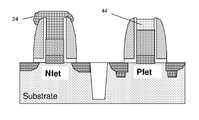
- FIG. 7shows a top view of a final structure and respective processing steps in accordance with the invention.
- FIG. 8shows a cross-sectional view of FIG. 7 along lines A-A.
- an epitaxially grown strain material 24is grown in the recess 22 of FIG. 6 .
- the strain material 24can extend above the structure to a height of about 30 nm to 50 nm; although, in embodiments, the strain material 24 is preferably planar or substantially planar with the surface of the structure.
- the strain material 24can be SiGe to provide a tensile strain for an NFET device.
- the strain material 24can be Si:C to provide a compressive strain for a PFET device.
- the SiGe materialwill provide a tensile stress in the channel of the NFET. More specifically, to increase the strain levels in a NFET device, the epitaxially grown SiGe layer, in an unrelaxed state, will have a lattice constant that conforms to that of the underlying polysilicon layer. Upon relaxation (e.g., through a high temperature process for example), the SiGe lattice constant approaches that of its intrinsic lattice constant which is larger than that of the underlying polysilicon layer.
- the underlying polysilicon layerconforms to the larger lattice constant of the relaxed SiGe layer which results in a physical biaxial strain (e.g., expansion) to the polysilicon layer.
- This physical strain applied to the polysilicon layeris beneficial because the expanded polysilicon layer increases N type device performance.
- the Si:C materialwill provide a compressive strain in the channel of the PFET. More specifically, to increase the strain levels in a PFET device, the epitaxially grown Si:C layer, in an unrelaxed state, will have a lattice constant that conforms to that of the underlying polysilicon layer. Upon relaxation (e.g., through a high temperature process for example), the Si:C lattice constant approaches that of its intrinsic lattice constant which is smaller than that of the underlying polysilicon layer.
- the polysilicon layerconforms to the smaller lattice constant of the relaxed Si:C layer which results in a physical biaxial strain (e.g., contraction) to the polysilicon layer.
- This physical strain applied to the polysilicon layeris beneficial because the contracted polysilicon layer increases P type device performance.
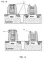
- FIG. 9shows a starting structure in accordance with another aspect of the invention. More particularly, the starting structure of FIG. 9 includes a beginning structure for an NFET and PFET, isolated from one another by an STI structure. The beginning structures for the NFET and PFET are fabricated according to the processes shown in FIGS. 1-5 .
- the STI structureis formed in a conventional manner using photolithographic and etching processes to form a trench.
- the trenchis then filled with an oxide, for example.
- a gate oxide layer 12is deposited over an active area of a wafer 10 in a conventional deposition process (as discussed with reference to FIG. 1 ).
- a polysilicon 14 and an SiGe material 16are deposited over the gate oxide layer 12 .
- a gate stackis then patterned in accordance with the processes shown, for example, in FIGS. 2-4 . Sidewalls and spacers 20 are formed using conventional processes as described with reference to FIG. 5 .
- a resist 26is formed over the NFET of FIG. 9 . Thereafter, as shown in FIG. 11 , an etching process will remove the SiGe layer of the PFET to form a recess 28 , as the resist 26 protects the NFET side of the device. The resist 26 is stripped away using a conventional stripping process.
- an oxide 30is formed over the structure of FIG. 11 .
- the oxide 30can be formed using any conventional oxidation process.
- the oxideis planarized using a conventional chemical mechanical polishing process.
- oxide 30remains within the recess 28 of the PFET.
- FIG. 14shows an intermediate structure and respective processing steps in accordance with the invention. More specifically, in FIG. 14 , a resist 32 is formed over the NFET structure. An etching process, e.g., SiO 2 Reactive Ion Etching (RIE), removes the oxide layer on the wafer and sidewall structure of the PFET.
- RIEReactive Ion Etching
- recesses 36are formed in the wafer, e.g., substrate, using a conventional RIE process.
- the recesses 36are formed in the source/drain regions of the PFET. During this processing, the NFET structure remains protected by a resist.
- the resist and the SiGe layer on the NFET stackare removed using a conventional stripping and etching processes known to those of skill in the art.
- a SiGe material 38is epitaxially grown in the recess of the NFET stack and the recesses 36 . As discussed above, the epitaxially grown SiGe will create tensile and compressive strains in the channels of the NFET and PFET, respectively.
- FIG. 17shows the removal of the remaining oxide layer about the NFET and on the polysilicon 14 of the PFET stack.
- the removal of the oxide layer on the PFET stackresults in a recess 40 .
- a silicidation processis performed, e.g., a high temperature anneal, over the structure of FIG. 17 to form silicide 42 .
- the silicide 42is formed in the source and drain regions of the NFET and the PFET.
- the silicide 42is formed on the NFET and PFET stacks.
- the silicide and SiGe layerare removed from the NFET stack to form a recess (not shown), and the silicide layer is removed from the PFET stack.
- An epitaxially grown strain material 24is provided in the recess formed in the NFET stack (similar to that shown in FIGS. 7 and 8 ). As disclosed above, the strain material 24 can extend above the structure; although, in embodiments, the strain material 24 is preferably planar or substantially planar with the surface of the structure. In embodiments, the strain material 24 can be an SiGe material to provide a tensile strain for an NFET device (in the manner disclosed above). An oxide cap 44 is formed on the remaining portion of the PFET stack in a conventional manner, which should be known to those of skill in the art.
- the methods as described aboveare used in the fabrication of integrated circuit chips.
- the resulting integrated circuit chipscan be distributed by the fabricator in raw wafer form (that is, as a single wafer that has multiple unpackaged chips), as a bare die, or in a packaged form.
- the chipis mounted in a single chip package (such as a plastic carrier, with leads that are affixed to a motherboard or other higher level carrier) or in a multichip package (such as a ceramic carrier that has either or both surface interconnections or buried interconnections).
- the chipis then integrated with other chips, discrete circuit elements, and/or other signal processing devices as part of either (a) an intermediate product, such as a motherboard, or (b) an end product.
- the end productcan be any product that includes integrated circuit chips, ranging from toys and other low-end applications to advanced computer products having a display, a keyboard or other input device, and a central processor.
Landscapes
- Engineering & Computer Science (AREA)
- Physics & Mathematics (AREA)
- Condensed Matter Physics & Semiconductors (AREA)
- General Physics & Mathematics (AREA)
- Manufacturing & Machinery (AREA)
- Computer Hardware Design (AREA)
- Microelectronics & Electronic Packaging (AREA)
- Power Engineering (AREA)
- Insulated Gate Type Field-Effect Transistor (AREA)
- Metal-Oxide And Bipolar Metal-Oxide Semiconductor Integrated Circuits (AREA)
- Chemical & Material Sciences (AREA)
- Materials Engineering (AREA)
Abstract
Description
Claims (10)
Priority Applications (5)
| Application Number | Priority Date | Filing Date | Title |
|---|---|---|---|
| US12/047,376US8293631B2 (en) | 2008-03-13 | 2008-03-13 | Semiconductor devices having tensile and/or compressive stress and methods of manufacturing |
| US13/364,753US8889504B2 (en) | 2008-03-13 | 2012-02-02 | Semiconductor devices having tensile and/or compressive stress and methods of manufacturing |
| US13/424,613US8896069B2 (en) | 2008-03-13 | 2012-03-20 | Semiconductor devices having tensile and/or compressive stress and methods of manufacturing |
| US14/515,981US9431535B2 (en) | 2008-03-13 | 2014-10-16 | Semiconductor devices having tensile and/or compressive stress and methods of manufacturing |
| US14/516,000US9276111B2 (en) | 2008-03-13 | 2014-10-16 | Semiconductor devices having tensile and/or compressive stress and methods of manufacturing |
Applications Claiming Priority (1)
| Application Number | Priority Date | Filing Date | Title |
|---|---|---|---|
| US12/047,376US8293631B2 (en) | 2008-03-13 | 2008-03-13 | Semiconductor devices having tensile and/or compressive stress and methods of manufacturing |
Related Child Applications (2)
| Application Number | Title | Priority Date | Filing Date |
|---|---|---|---|
| US13/364,753ContinuationUS8889504B2 (en) | 2008-03-13 | 2012-02-02 | Semiconductor devices having tensile and/or compressive stress and methods of manufacturing |
| US13/424,613DivisionUS8896069B2 (en) | 2008-03-13 | 2012-03-20 | Semiconductor devices having tensile and/or compressive stress and methods of manufacturing |
Publications (2)
| Publication Number | Publication Date |
|---|---|
| US20090230427A1 US20090230427A1 (en) | 2009-09-17 |
| US8293631B2true US8293631B2 (en) | 2012-10-23 |
Family
ID=41062055
Family Applications (5)
| Application Number | Title | Priority Date | Filing Date |
|---|---|---|---|
| US12/047,376Active2031-02-26US8293631B2 (en) | 2008-03-13 | 2008-03-13 | Semiconductor devices having tensile and/or compressive stress and methods of manufacturing |
| US13/364,753Expired - Fee RelatedUS8889504B2 (en) | 2008-03-13 | 2012-02-02 | Semiconductor devices having tensile and/or compressive stress and methods of manufacturing |
| US13/424,613Expired - Fee RelatedUS8896069B2 (en) | 2008-03-13 | 2012-03-20 | Semiconductor devices having tensile and/or compressive stress and methods of manufacturing |
| US14/515,981Expired - Fee RelatedUS9431535B2 (en) | 2008-03-13 | 2014-10-16 | Semiconductor devices having tensile and/or compressive stress and methods of manufacturing |
| US14/516,000Expired - Fee RelatedUS9276111B2 (en) | 2008-03-13 | 2014-10-16 | Semiconductor devices having tensile and/or compressive stress and methods of manufacturing |
Family Applications After (4)
| Application Number | Title | Priority Date | Filing Date |
|---|---|---|---|
| US13/364,753Expired - Fee RelatedUS8889504B2 (en) | 2008-03-13 | 2012-02-02 | Semiconductor devices having tensile and/or compressive stress and methods of manufacturing |
| US13/424,613Expired - Fee RelatedUS8896069B2 (en) | 2008-03-13 | 2012-03-20 | Semiconductor devices having tensile and/or compressive stress and methods of manufacturing |
| US14/515,981Expired - Fee RelatedUS9431535B2 (en) | 2008-03-13 | 2014-10-16 | Semiconductor devices having tensile and/or compressive stress and methods of manufacturing |
| US14/516,000Expired - Fee RelatedUS9276111B2 (en) | 2008-03-13 | 2014-10-16 | Semiconductor devices having tensile and/or compressive stress and methods of manufacturing |
Country Status (1)
| Country | Link |
|---|---|
| US (5) | US8293631B2 (en) |
Cited By (2)
| Publication number | Priority date | Publication date | Assignee | Title |
|---|---|---|---|---|
| US9349734B2 (en)* | 2014-09-03 | 2016-05-24 | Globalfoundries Inc. | Selective FuSi gate formation in gate first CMOS technologies |
| US9419097B2 (en) | 2014-11-24 | 2016-08-16 | International Business Machines Corporation | Replacement metal gate dielectric cap |
Families Citing this family (12)
| Publication number | Priority date | Publication date | Assignee | Title |
|---|---|---|---|---|
| US8293631B2 (en) | 2008-03-13 | 2012-10-23 | International Business Machines Corporation | Semiconductor devices having tensile and/or compressive stress and methods of manufacturing |
| US20090309163A1 (en)* | 2008-06-11 | 2009-12-17 | International Business Machines Corporation | Method and structure for enhancing both nmosfet and pmosfet performance with a stressed film and discontinuity extending to underlying layer |
| US8729627B2 (en) | 2010-05-14 | 2014-05-20 | Taiwan Semiconductor Manufacturing Company, Ltd. | Strained channel integrated circuit devices |
| US9620619B2 (en)* | 2012-01-12 | 2017-04-11 | Globalfoundries Inc. | Borderless contact structure |
| US8753969B2 (en)* | 2012-01-27 | 2014-06-17 | GlobalFoundries, Inc. | Methods for fabricating MOS devices with stress memorization |
| CN103489777A (en)* | 2012-06-11 | 2014-01-01 | 中芯国际集成电路制造(上海)有限公司 | Stress memory technology method |
| CN103489765B (en)* | 2012-06-11 | 2016-06-22 | 中芯国际集成电路制造(上海)有限公司 | The manufacture method of NMOS metal gate electrode |
| KR20140108982A (en)* | 2013-03-04 | 2014-09-15 | 삼성전자주식회사 | Memory device and method for fabrication the device |
| CN104347374A (en)* | 2013-07-30 | 2015-02-11 | 北大方正集团有限公司 | Manufacturing method of semiconductor device |
| CN106409765B (en)* | 2015-07-31 | 2020-03-10 | 中芯国际集成电路制造(上海)有限公司 | Semiconductor structure and forming method thereof |
| US9443873B1 (en) | 2015-12-14 | 2016-09-13 | International Business Machines Corporation | Structure and method for tensile and compressive strained silicon germanium with same germanium concentration by single epitaxy step |
| US10593672B2 (en) | 2018-01-08 | 2020-03-17 | International Business Machines Corporation | Method and structure of forming strained channels for CMOS device fabrication |
Citations (12)
| Publication number | Priority date | Publication date | Assignee | Title |
|---|---|---|---|---|
| US6165826A (en)* | 1994-12-23 | 2000-12-26 | Intel Corporation | Transistor with low resistance tip and method of fabrication in a CMOS process |
| US6872625B2 (en) | 2000-05-22 | 2005-03-29 | Max-Planck-Gesellschaft Zur Foerderung Der Wissenschaften E.V. | Field-effect transistor based on embedded cluster structures and process for its production |
| US20050112817A1 (en)* | 2003-11-25 | 2005-05-26 | Taiwan Semiconductor Manufacturing Company, Ltd. | Semiconductor device having high drive current and method of manufacture thereof |
| US20050236668A1 (en)* | 2004-04-23 | 2005-10-27 | International Business Machines Corporation | STRUCTURES AND METHODS FOR MANUFACTURING OF DISLOCATION FREE STRESSED CHANNELS IN BULK SILICON AND SOI CMOS DEVICES BY GATE STRESS ENGINEERING WITH SiGe AND/OR Si:C |
| US20060194387A1 (en) | 2005-02-25 | 2006-08-31 | Chih-Hao Wang | High performance transistors with SiGe strain |
| US20060234455A1 (en) | 2005-04-19 | 2006-10-19 | Chien-Hao Chen | Structures and methods for forming a locally strained transistor |
| US20070015334A1 (en)* | 2005-07-11 | 2007-01-18 | Interuniversitair Microelektronica Centrum (Imec) | Method for forming a fully silicided gate and devices obtained thereof |
| US20070057324A1 (en) | 2005-09-13 | 2007-03-15 | Tews Helmut H | Strained semiconductor device and method of making the same |
| US7217603B2 (en) | 2002-06-25 | 2007-05-15 | Amberwave Systems Corporation | Methods of forming reacted conductive gate electrodes |
| US20080009110A1 (en)* | 2006-07-05 | 2008-01-10 | Tzu-Yun Chang | Metal-oxide semiconductor field effect transistor and method for manufacturing the same |
| US20080119019A1 (en)* | 2006-11-20 | 2008-05-22 | Jin-Ping Han | Semiconductor devices having pFET with SiGe gate electrode and embedded SiGe source/drain regions and methods of making the same |
| US7462524B1 (en)* | 2005-08-16 | 2008-12-09 | Advanced Micro Devices, Inc. | Methods for fabricating a stressed MOS device |
Family Cites Families (6)
| Publication number | Priority date | Publication date | Assignee | Title |
|---|---|---|---|---|
| US5827747A (en) | 1996-03-28 | 1998-10-27 | Mosel Vitelic, Inc. | Method for forming LDD CMOS using double spacers and large-tilt-angle ion implantation |
| TW497120B (en) | 2000-03-06 | 2002-08-01 | Toshiba Corp | Transistor, semiconductor device and manufacturing method of semiconductor device |
| US7348232B2 (en)* | 2005-03-01 | 2008-03-25 | Texas Instruments Incorporated | Highly activated carbon selective epitaxial process for CMOS |
| US7238561B2 (en)* | 2005-08-02 | 2007-07-03 | Freescale Semiconductor, Inc. | Method for forming uniaxially strained devices |
| US8304342B2 (en)* | 2006-10-31 | 2012-11-06 | Texas Instruments Incorporated | Sacrificial CMP etch stop layer |
| US8293631B2 (en)* | 2008-03-13 | 2012-10-23 | International Business Machines Corporation | Semiconductor devices having tensile and/or compressive stress and methods of manufacturing |
- 2008
- 2008-03-13USUS12/047,376patent/US8293631B2/enactiveActive
- 2012
- 2012-02-02USUS13/364,753patent/US8889504B2/ennot_activeExpired - Fee Related
- 2012-03-20USUS13/424,613patent/US8896069B2/ennot_activeExpired - Fee Related
- 2014
- 2014-10-16USUS14/515,981patent/US9431535B2/ennot_activeExpired - Fee Related
- 2014-10-16USUS14/516,000patent/US9276111B2/ennot_activeExpired - Fee Related
Patent Citations (12)
| Publication number | Priority date | Publication date | Assignee | Title |
|---|---|---|---|---|
| US6165826A (en)* | 1994-12-23 | 2000-12-26 | Intel Corporation | Transistor with low resistance tip and method of fabrication in a CMOS process |
| US6872625B2 (en) | 2000-05-22 | 2005-03-29 | Max-Planck-Gesellschaft Zur Foerderung Der Wissenschaften E.V. | Field-effect transistor based on embedded cluster structures and process for its production |
| US7217603B2 (en) | 2002-06-25 | 2007-05-15 | Amberwave Systems Corporation | Methods of forming reacted conductive gate electrodes |
| US20050112817A1 (en)* | 2003-11-25 | 2005-05-26 | Taiwan Semiconductor Manufacturing Company, Ltd. | Semiconductor device having high drive current and method of manufacture thereof |
| US20050236668A1 (en)* | 2004-04-23 | 2005-10-27 | International Business Machines Corporation | STRUCTURES AND METHODS FOR MANUFACTURING OF DISLOCATION FREE STRESSED CHANNELS IN BULK SILICON AND SOI CMOS DEVICES BY GATE STRESS ENGINEERING WITH SiGe AND/OR Si:C |
| US20060194387A1 (en) | 2005-02-25 | 2006-08-31 | Chih-Hao Wang | High performance transistors with SiGe strain |
| US20060234455A1 (en) | 2005-04-19 | 2006-10-19 | Chien-Hao Chen | Structures and methods for forming a locally strained transistor |
| US20070015334A1 (en)* | 2005-07-11 | 2007-01-18 | Interuniversitair Microelektronica Centrum (Imec) | Method for forming a fully silicided gate and devices obtained thereof |
| US7462524B1 (en)* | 2005-08-16 | 2008-12-09 | Advanced Micro Devices, Inc. | Methods for fabricating a stressed MOS device |
| US20070057324A1 (en) | 2005-09-13 | 2007-03-15 | Tews Helmut H | Strained semiconductor device and method of making the same |
| US20080009110A1 (en)* | 2006-07-05 | 2008-01-10 | Tzu-Yun Chang | Metal-oxide semiconductor field effect transistor and method for manufacturing the same |
| US20080119019A1 (en)* | 2006-11-20 | 2008-05-22 | Jin-Ping Han | Semiconductor devices having pFET with SiGe gate electrode and embedded SiGe source/drain regions and methods of making the same |
Cited By (4)
| Publication number | Priority date | Publication date | Assignee | Title |
|---|---|---|---|---|
| US9349734B2 (en)* | 2014-09-03 | 2016-05-24 | Globalfoundries Inc. | Selective FuSi gate formation in gate first CMOS technologies |
| US9419097B2 (en) | 2014-11-24 | 2016-08-16 | International Business Machines Corporation | Replacement metal gate dielectric cap |
| US9620622B2 (en) | 2014-11-24 | 2017-04-11 | International Business Machines Corporation | Replacement metal gate dielectric cap |
| US9685530B2 (en) | 2014-11-24 | 2017-06-20 | International Business Machines Corporation | Replacement metal gate dielectric cap |
Also Published As
| Publication number | Publication date |
|---|---|
| US20120175640A1 (en) | 2012-07-12 |
| US8889504B2 (en) | 2014-11-18 |
| US20150037957A1 (en) | 2015-02-05 |
| US20120135591A1 (en) | 2012-05-31 |
| US9431535B2 (en) | 2016-08-30 |
| US20150054028A1 (en) | 2015-02-26 |
| US8896069B2 (en) | 2014-11-25 |
| US9276111B2 (en) | 2016-03-01 |
| US20090230427A1 (en) | 2009-09-17 |
Similar Documents
| Publication | Publication Date | Title |
|---|---|---|
| US8293631B2 (en) | Semiconductor devices having tensile and/or compressive stress and methods of manufacturing | |
| US7791144B2 (en) | High performance stress-enhance MOSFET and method of manufacture | |
| US8119472B2 (en) | Silicon device on Si:C SOI and SiGe and method of manufacture | |
| US7432149B2 (en) | CMOS on SOI substrates with hybrid crystal orientations | |
| US7704839B2 (en) | Buried stress isolation for high-performance CMOS technology | |
| US20070269963A1 (en) | STRAINED HOT (HYBRID ORIENTATION TECHNOLOGY) MOSFETs | |
| US20080128765A1 (en) | MOSFET Device With Localized Stressor | |
| KR20070024581A (en) | Semiconductor device with multiple semiconductor layers | |
| US9564488B2 (en) | Strained isolation regions | |
| US7772095B2 (en) | Integrated circuit having localized embedded SiGe and method of manufacturing | |
| KR101126913B1 (en) | Raised sti structure and superdamascene technique for nmosfet performance enhancement with embedded silicon carbon | |
| US7615418B2 (en) | High performance stress-enhance MOSFET and method of manufacture | |
| US9559018B2 (en) | Dual channel finFET with relaxed pFET region | |
| US9368410B2 (en) | Semiconductor devices having tensile and/or compressive stress and methods of manufacturing | |
| CN117913094A (en) | Device with laterally graded channel region |
Legal Events
| Date | Code | Title | Description |
|---|---|---|---|
| AS | Assignment | Owner name:INTERNATIONAL BUSINESS MACHINES CORPORATION, NEW Y Free format text:ASSIGNMENT OF ASSIGNORS INTEREST;ASSIGNORS:DYER, THOMAS W;YANG, HAINING S;REEL/FRAME:020644/0010;SIGNING DATES FROM 20080305 TO 20080306 Owner name:INTERNATIONAL BUSINESS MACHINES CORPORATION, NEW Y Free format text:ASSIGNMENT OF ASSIGNORS INTEREST;ASSIGNORS:DYER, THOMAS W;YANG, HAINING S;SIGNING DATES FROM 20080305 TO 20080306;REEL/FRAME:020644/0010 | |
| STCF | Information on status: patent grant | Free format text:PATENTED CASE | |
| AS | Assignment | Owner name:GLOBALFOUNDRIES U.S. 2 LLC, NEW YORK Free format text:ASSIGNMENT OF ASSIGNORS INTEREST;ASSIGNOR:INTERNATIONAL BUSINESS MACHINES CORPORATION;REEL/FRAME:036550/0001 Effective date:20150629 | |
| AS | Assignment | Owner name:GLOBALFOUNDRIES INC., CAYMAN ISLANDS Free format text:ASSIGNMENT OF ASSIGNORS INTEREST;ASSIGNORS:GLOBALFOUNDRIES U.S. 2 LLC;GLOBALFOUNDRIES U.S. INC.;REEL/FRAME:036779/0001 Effective date:20150910 | |
| FPAY | Fee payment | Year of fee payment:4 | |
| AS | Assignment | Owner name:WILMINGTON TRUST, NATIONAL ASSOCIATION, DELAWARE Free format text:SECURITY AGREEMENT;ASSIGNOR:GLOBALFOUNDRIES INC.;REEL/FRAME:049490/0001 Effective date:20181127 | |
| MAFP | Maintenance fee payment | Free format text:PAYMENT OF MAINTENANCE FEE, 8TH YEAR, LARGE ENTITY (ORIGINAL EVENT CODE: M1552); ENTITY STATUS OF PATENT OWNER: LARGE ENTITY Year of fee payment:8 | |
| AS | Assignment | Owner name:GLOBALFOUNDRIES U.S. INC., CALIFORNIA Free format text:ASSIGNMENT OF ASSIGNORS INTEREST;ASSIGNOR:GLOBALFOUNDRIES INC.;REEL/FRAME:054633/0001 Effective date:20201022 | |
| AS | Assignment | Owner name:GLOBALFOUNDRIES INC., CAYMAN ISLANDS Free format text:RELEASE BY SECURED PARTY;ASSIGNOR:WILMINGTON TRUST, NATIONAL ASSOCIATION;REEL/FRAME:054636/0001 Effective date:20201117 | |
| AS | Assignment | Owner name:GLOBALFOUNDRIES U.S. INC., NEW YORK Free format text:RELEASE BY SECURED PARTY;ASSIGNOR:WILMINGTON TRUST, NATIONAL ASSOCIATION;REEL/FRAME:056987/0001 Effective date:20201117 | |
| MAFP | Maintenance fee payment | Free format text:PAYMENT OF MAINTENANCE FEE, 12TH YEAR, LARGE ENTITY (ORIGINAL EVENT CODE: M1553); ENTITY STATUS OF PATENT OWNER: LARGE ENTITY Year of fee payment:12 |