US8293619B2 - Layer transfer of films utilizing controlled propagation - Google Patents
Layer transfer of films utilizing controlled propagationDownload PDFInfo
- Publication number
- US8293619B2 US8293619B2US12/460,898US46089809AUS8293619B2US 8293619 B2US8293619 B2US 8293619B2US 46089809 AUS46089809 AUS 46089809AUS 8293619 B2US8293619 B2US 8293619B2
- Authority
- US
- United States
- Prior art keywords
- film
- energy
- thermal
- cleaving
- cleave
- Prior art date
- Legal status (The legal status is an assumption and is not a legal conclusion. Google has not performed a legal analysis and makes no representation as to the accuracy of the status listed.)
- Expired - Fee Related, expires
Links
Images


Classifications
- H—ELECTRICITY
- H01—ELECTRIC ELEMENTS
- H01L—SEMICONDUCTOR DEVICES NOT COVERED BY CLASS H10
- H01L21/00—Processes or apparatus adapted for the manufacture or treatment of semiconductor or solid state devices or of parts thereof
- H01L21/02—Manufacture or treatment of semiconductor devices or of parts thereof
- H01L21/04—Manufacture or treatment of semiconductor devices or of parts thereof the devices having potential barriers, e.g. a PN junction, depletion layer or carrier concentration layer
- H01L21/18—Manufacture or treatment of semiconductor devices or of parts thereof the devices having potential barriers, e.g. a PN junction, depletion layer or carrier concentration layer the devices having semiconductor bodies comprising elements of Group IV of the Periodic Table or AIIIBV compounds with or without impurities, e.g. doping materials
- H01L21/30—Treatment of semiconductor bodies using processes or apparatus not provided for in groups H01L21/20 - H01L21/26
- H—ELECTRICITY
- H10—SEMICONDUCTOR DEVICES; ELECTRIC SOLID-STATE DEVICES NOT OTHERWISE PROVIDED FOR
- H10F—INORGANIC SEMICONDUCTOR DEVICES SENSITIVE TO INFRARED RADIATION, LIGHT, ELECTROMAGNETIC RADIATION OF SHORTER WAVELENGTH OR CORPUSCULAR RADIATION
- H10F71/00—Manufacture or treatment of devices covered by this subclass
- H—ELECTRICITY
- H01—ELECTRIC ELEMENTS
- H01L—SEMICONDUCTOR DEVICES NOT COVERED BY CLASS H10
- H01L21/00—Processes or apparatus adapted for the manufacture or treatment of semiconductor or solid state devices or of parts thereof
- H01L21/70—Manufacture or treatment of devices consisting of a plurality of solid state components formed in or on a common substrate or of parts thereof; Manufacture of integrated circuit devices or of parts thereof
- H01L21/71—Manufacture of specific parts of devices defined in group H01L21/70
- H01L21/76—Making of isolation regions between components
- H01L21/762—Dielectric regions, e.g. EPIC dielectric isolation, LOCOS; Trench refilling techniques, SOI technology, use of channel stoppers
- H01L21/7624—Dielectric regions, e.g. EPIC dielectric isolation, LOCOS; Trench refilling techniques, SOI technology, use of channel stoppers using semiconductor on insulator [SOI] technology
- H01L21/76251—Dielectric regions, e.g. EPIC dielectric isolation, LOCOS; Trench refilling techniques, SOI technology, use of channel stoppers using semiconductor on insulator [SOI] technology using bonding techniques
- H01L21/76254—Dielectric regions, e.g. EPIC dielectric isolation, LOCOS; Trench refilling techniques, SOI technology, use of channel stoppers using semiconductor on insulator [SOI] technology using bonding techniques with separation/delamination along an ion implanted layer, e.g. Smart-cut, Unibond
Definitions
- the silicon solar cellgenerates electrical power when exposed to solar radiation from the sun.
- the radiationinteracts with atoms of the silicon and forms electrons and holes that migrate to p-doped and n-doped regions in the silicon body and create voltage differentials and an electric current between the doped regions.
- Solar cellshave been integrated with concentrating elements to improve efficiency. As an example, solar radiation accumulates and focuses using concentrating elements that direct such radiation to one or more portions of active photovoltaic materials. Although effective, these solar cells still have many limitations.
- solar cellsoften rely upon starting materials such as silicon.
- siliconis often made using either polysilicon and/or single crystal silicon materials.
- Polysilicon materialcan also, depending on the size of single-crystal grains and degree of crystallinity, called multicrystalline, microcrystalline, or nanocrystalline. These materials will henceforth be called “polysilicon”, as opposed to single crystal (monocrystalline) material which does not have numerous random crystal orientations and numerous grain boundaries.
- Amorphous siliconis not a form of silicon commonly used in wafered solar cells due to its poor carrier lifetime in thicknesses less than a few microns.
- Polysilicon cellsare often formed by manufacturing polysilicon plates. Although these plates may be formed in a cost effective manner using crystallization furnaces, they do not possess optimum properties for highly effective solar cells. In particular, polysilicon plates do not exhibit the highest possible efficiency in capturing solar energy and converting the captured solar energy into usable electrical power.
- single crystal silicon(c-Si) has suitable properties for high grade solar cells.
- Such single crystal siliconis, however, expensive to manufacture and is also difficult to use for solar applications in an efficient and cost effective manner.
- both polysilicon and single-crystal silicon materialssuffer from material losses during conventional manufacturing single crystal silicon substrates, where a sawing process is used to physically separate thin single crystal silicon layers from a single crystal silicon ingot originally grown.
- a sawing processis used to physically separate thin single crystal silicon layers from a single crystal silicon ingot originally grown.
- inner diameter (ID) sawing process or wire sawing processeliminates as much as 40% and even up to 60% of the starting material from a cast or grown boule and singulate the material into a wafer form factor. This is a highly inefficient method of preparing thin polysilicon or single-crystal silicon plates for solar cell use.
- Thin film solar cellsare often less expensive by using less silicon material or alternative materials but their amorphous or polycrystalline structure are less efficient than the more expensive bulk silicon cells made from single-crystal silicon substrates.
- a film of materialmay be formed by providing a semiconductor substrate having a surface region and a cleave region located at a predetermined depth beneath the surface region. During a process of cleaving the film from the substrate, shear in the cleave region is carefully controlled. According to certain embodiments, an in-plane shear component (KII) is maintained near zero at a certain film thickness to maintain a propagating cleave plane within the desired depth. In one embodiment, the near-zero KII component is achieved by adiabatic heating of silicon through exposure to E-beam radiation, which can impart thermally generated forces and moments to achieve the desired KII condition.
- KIIin-plane shear component
- the KII componentis purposefully maintained at a high level by an implant and optional external energy to guide fracture propagation using an energy control method.
- the high KII componentis achieved by heating of the silicon through exposure to radiation such as laser or E-beam, which imparts a thermal gradient to achieve controlled propagation at a precisely defined depth in the silicon through depth dependent cleave energy control.
- Embodiments of the present inventionrelate generally to layer transfer techniques for forming thick films. More particularly, the present invention provides a method and device for low or even implant free layer transfer of thick films for solar cells. Merely by example, it is applied to cleave thick films along a crystallographic plane of single crystal silicon substrate. But it will be recognized that the invention has a wider range of applicability.
- single crystal silicon ingot substrate with a surface plane in an ⁇ 111 ⁇ or ⁇ 110 ⁇ crystallographic planecan be selected.
- the ion implantation process for creating cleave regioncan be mostly eliminated or limited to form a cleave initiation region with a portion of peripheral region. This substantially simplifies the layer transfer process, reduces system energy cost and increases productivity.
- the processis divided into (i) an initiation process utilizing a higher implant dose (the initiation dose) to initiate a fracture in a relatively small area of the silicon ingot substrate (the initiation region), and (ii) a propagation process that extends the initiated crack tip through the remainder of the silicon ingot substrate to release the thick film (the propagation region). Since the propagation process must extend the initiation region through the majority of the surface area of the thick film to be released, this process should operate reliably with a small implant dose, and perhaps without any dose. This is called the propagation dose, and the total dose needed for the process would therefore be the weighted area average of the imitation and propagation dose.
- the total effective doseis 0.01*6 ⁇ 10 16 cm ⁇ 2 +0.99*1 ⁇ 10 16 cm ⁇ 2 or 1.05 ⁇ 10 16 cm ⁇ 2 . Reducing or eliminating the propagation dose will have a first order effect on the total dose requirement for this cleaving process.
- Lowering of the dosein turn depends on (i) optimizing the effect of the implanted hydrogen to maximize its cleave guiding action and (ii) optimizing the cleave process by generating the right stress intensity conditions at the crack tip to keep the cleave front within the desired depth without breaking or cracking the film.
- Embodiments in accordance with the present inventionare directed to optimizing the mechanical configuration during the cleave propagation process.
- the cleave initiation regioncan be created in a patterned implantation by irradiating high energy ionic particles with controlled dosage generated using a linear accelerator.
- the present inventionprovides a mechanical moment loading with a force loading (generated through an appropriate thermal treatment process and/or mechanical forces) to generate a stress gradient such that a substantially zero shear region can be formed despite the natural tendency of the mechanical configuration to generate mixed-mode loading.
- a high quality thick film crystalline materialhaving a thickness ranging from a few tens of microns to a few hundreds of microns, can be produced with kerf loss substantially lower than possible utilizing conventional techniques.
- the resulting single crystal silicon thick filmsare particularly suited for use in high efficiency (20% or higher) photovoltaic cells.
- Some embodimentscan utilize existing manufacture processing systems and techniques, and take some advantage of certain newly developed techniques for manufacturing thin wafer/substrate for various semiconductor device applications. More details about various embodiments of the present invention can be found in the description below.
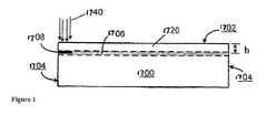
- FIG. 1is a simplified diagram showing a formation of a cleave initiation region by patterned implanting high energy particles according to an embodiment of the present invention.
- FIG. 2shows a simplified schematic view of the general case of propagation.
- FIG. 3shows hydrogen layer stress profile model.
- FIG. 3Ashows an example of an energy calculator utilizing the model.
- FIG. 4shows a simplified matrix of available thermal loading configurations.
- FIG. 5shows a graph of the cleaving regimes available as a function of time scale of thermal loading application.
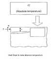
- FIG. 6Ashows the concept of heat soak to raise absolute temperature within the cleave plane area.
- FIG. 6Bshows the concept of heat pulse to generate a film-substrate temperature differential.
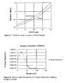
- FIG. 7shows a plot of maximum electron depth versus energy (CSDA Range).
- FIG. 8shows Monte Carlo simulation of E-beam volumetric energy deposition profile in silicon.
- FIG. 9shows a simulated E-Beam profile to achieve KII controlled propagation cleaving.
- FIG. 10shows stress intensity and energy result using adiabatic E-Beam KII controlled propagation.
- FIG. 11shows an energy-stress deposition profile using E-Beam.
- Particular embodiments of the present inventionprovide a method and device for layer transfer of thick films for solar cells.
- itis applied to cleave thick films along a crystallographic plane of single crystal silicon substrate.
- the inventionhas a wider range of applicability.
- other materialssuch as Germanium, Gallium Arsenide (GaAs), Gallium Nitride (GaN), or Silicon Carbide (SiC) could be subjected to the cleaving process to release films of materials for solar, opto-electronic or semiconductor applications.
- a solutionis to use a high energy ion beam to create a cleave region at a desired thickness beneath the substrate surface, then perform a layer transfer process to free the thickness of film from remaining substrate.
- use of only implanted ions to create a cleave region susceptible for cleavingmay require a high ion dose and an extended implanting area.
- implanted ionsmay result in higher surface roughness, added cost with high ion dose and less productivity, and potentially lower yields and film quality.
- these and other limitationsare overcome using the present method and structures.
- cleaving of a film of materialmay be accomplished with substantially reduced implantation of ions, or possibly no implantation at all, utilizing a cleaving process that carefully controls the shear conditions during the cleaving.
- a film of materialmay be formed by providing a semiconductor substrate having a surface region, a peripheral region, and a cleave region at a predetermined depth beneath the surface region.
- the term “cleave region”does not necessarily denote a region that has received radiation or implanted ions, but rather refers to a region that may be separated from the substrate following the application of radiation and/or implanted ions.
- a cleave initiation regionmay be defined within a portion of the peripheral region and a vicinity of the cleave region.
- the cleave initiation regionmay be formed by subjecting the region to a thermal, chemical, electrical, and/or mechanical process to spall or release a section of the film within the initiation region.
- initiation cleavingis accomplished by subjecting the cleave initiation region to a localized thermal treatment, so that a cleave front can be initiated within this region and propagates to the periphery of the initiation region where the dose is lower and does not promote further propagation.
- the propagation areais controlled by the localized energy itself. The general film release process can then continue to propagate the initiated film from the existing cleave front through the remainder of the substrate.
- FIG. 1is a simplified diagram illustrating a side view of a semiconductor substrate having a cleave region at a predetermined depth beneath a surface region according to an embodiment of the present invention.
- This diagramis merely an example, which should not unduly limit the scope of the claims herein.
- One of ordinary skill in the artwould recognize many variations, alternatives, and modifications.
- a semiconductor substrate 1700is provided having a surface region 1702 and a peripheral region 1704 .
- a cleave region 1706is provided. This cleave region is in essence a virtual plane or layer located at a predetermined depth d beneath the surface region 1702 , and is used to define a thickness of thick film 1720 to be detached from the semiconductor substrate 1700 .
- the semiconductor substratehas a thickness substantially larger than the depth h.
- the semiconductor substrateis single crystal silicon material for use in a photovoltaic solar cell.
- the silicon substratehas a surface plane that is generally selected to be close to a ⁇ 111 ⁇ or ⁇ 110 ⁇ crystallographic plane (a certain small miscut angle of less than about 1° may exist).
- the cleave region definedis substantially parallel to the surface region. Since the cleaving action is energetically easier along the ⁇ 111 ⁇ plane followed by ⁇ 110 ⁇ plane than in the traditional ⁇ 100 ⁇ plane, it may be desirable to orient the material to be cleaved to coincide the surface to be cleaved with a lower surface energy crystallographic cleave plane. More detailed description of techniques for selecting certain orientation of the silicon boule for slicing or cleaving can be found in the U.S. Provisional Patent Application No.
- FIG. 1also shows the formation of a cleave initiation region by pattern implanting high energy particles according to an embodiment of the present invention.
- This diagramis merely an example, which should not unduly limit the scope of the claims herein.
- One of ordinary skill in the artwould recognize many variations, alternatives, and modifications.
- a portion of the peripheral region 1704can be associated with a predetermined patterned region (not shown directly in the cross-sectional view of FIG. 1 ) within the surface region 1702 .
- the selected portion of the peripheral regionis within an edge vicinity of the cleave region 1706 .
- the patterned region of the surface region 1702is exposed to a high energy ion beam 1740 , for example H+ ions with energy level of 1 MeV or more using a high-energy particle accelerator.
- a high energy ion beam 1740for example H+ ions with energy level of 1 MeV or more using a high-energy particle accelerator.
- the choice of acceleratorscan range from linear accelerators (electrostatic or RF driven types) or other non-linac types such as cyclotron accelerators.
- Ion implant apparatuses useful for embodiments of the present inventionhave been made recently available by the use of DC electrostatic particle accelerators such as the DYNAMITRON proton accelerator available from Ion Beam Applications SA, Belgium).
- DC electrostatic particle acceleratorssuch as the DYNAMITRON proton accelerator available from Ion Beam Applications SA, Belgium.
- Other forms of DC electrostatic accelerators which may be usedinclude Van de Graaff or Tandem Van de Graaff accelerator types.
- Still other forms of particle accelerators suitable for use in accordance with embodiments of the present inventionmay include radio frequency (RF) particle accelerators such as a cyclotron or a RF linear accelerator (RF Linac).
- RF particle acceleratorssuch as a cyclotron or a RF linear accelerator (RF Linac).
- RF Linacradio-frequency quadrupole linear accelerator
- DTLDrift-Tube Linac
- RFIDRadio-Focused Interdigitated
- the area of the patterned initiation regionis limited to 1-3% of the total substrate surface area (e.g., 2-5 cm 2 or less for a 125 mm ⁇ 125 mm sized substrate), so that the ion particle dose is well controlled minimize energy costs of the system and enhance productivity of the thick film cleaving process.
- the high energy ionsare implanted beneath the surface region to reach a region within the vicinity of the cleave region 1706 .
- the penetration depth of the ionsis dependent on the energy level, and can be controlled to a desired value that determines a depth h of the cleave region.
- the implanted ionsslow down within the crystal lattice by transferring kinetic energy to the lattice in the form of ionization (electronic braking), and small amount of atomic damage by displacing atoms (nuclear stopping).
- the ionsinteract substantially more with the crystal lattice under nuclear stopping, and a thin region of relatively high stress and damaged lattice bonds is formed to define a cleave initiation region 1708 .
- the formed cleave initiation region 1708is a small planar region extending from a portion of the peripheral region 1704 toward within the cleave region 1706 . Since the patterned implantation is performed by irradiating ionic particles within an area less than 1-3% of total area of surface region, this initiation dose can be higher than the propagation dose. This allows the averaged area dose to be maintained low for enhanced productivity. Of course, there can be many alternatives, variations, and modifications.
- Two forms of controlled propagationcan be utilized to reliably propagate a cleave within material 1700 to release a film of thickness h from the substrate and avoid cleave failure.
- the first form of controlled propagationis referred to as “KII controlled propagation”, while the second form of controlled propagation is referred to as “energy controlled propagation”.
- Both formscan control the propagating cleave plane at a desired depth to release a film of thickness h.
- these forms of controlled propagationaccomplish this goal utilizing different methods and approaches.
- Cleave failureis essentially defined as the unwanted branching of the cleave plane, usually resulting in fractured films. Avoidance of unwanted branching of the cleave plane is thus a consideration in the design of cleaving techniques. Other factors found to affect unwanted branching include crystal orientation and implant dose and depth and temperature profile, for example.
- thermal energy injected within the vicinity of the cleave plane and used to generate cleaving stresseswill be affected by the fact that the implanted cleave plane has a substantially lower thermal conductivity over unimplanted single-crystal silicon.
- This lower thermal conductivityis a result of the hydrogen implant damage and will tend to modify the temperature profile, which in turn will modify the cleaving stresses.
- a first form of controlled propagationis KII controlled propagation, and is defined as simultaneously achieving threshold cleave propagation energy G′ (defined below) with KII at or near zero.
- G′threshold cleave propagation energy
- LFMLinear Elastic Fracture Mechanics
- Stable KII controloccurs when small changes in depth generate a restoring KII shear of the level and sign so as to help turn the cleave plane towards the desired depth.
- a second form of controlled propagationis energy controlled propagation, and is characterized as a depth control where the threshold energy required to propagate the cleave plane changes such that below the desired depth, propagation is favored by a high KII factor but energetically cannot be supported.
- Cleaving by an implanted hydrogen layeris one example of energy controlled cleaving.
- LFMLinear Elastic Fracture Mechanics
- FIG. 2The mechanical configuration following the initiation process is shown in FIG. 2 .
- a thick film of thickness his partially released from the rest of the silicon ingot substrate having thickness H. Due to the much larger dimensions of the substrate relative to the cleaved material, h ⁇ H and the tile moment and forces M 2 , P 2 and M 3 , P 3 are understood to be very small.
- the source of stress intensity seen at the crack tipis thus dominated by M 1 and P 1 , the moment and force coupled to the partially released thick film.
- a basic concept of embodiments of the present inventionis the hydrogen cleave plane.
- the hydrogen cleave planeaffects the cleaving action through stress and layer weakening effects.
- the H-planecan be used both as an initiating layer at higher doses, and as a guiding or propagating layer when the dose is lower.
- the action of the H-layeris different within these two dosage regimes.
- the energy needed to create a new surface during cleavingis hereafter referred to as the surface energy ( ⁇ ).
- ⁇The energy needed to create a new surface during cleaving
- the surface energyis about 1.2 J/m 2 for the ⁇ 111 ⁇ orientation, although fracture toughness in silicon is sometimes reported as 4-6 J/m 2 and includes effects such as lattice trapping to give an effective energy to produce a new surface.
- a surface energy of 1.2 J/m 2 per surface2.4 J/m 2 total
- the value of the modified surface energy ( ⁇ ′) along an implanted cleave planecan be substantially lower, perhaps by a factor of 5 or more.
- the ⁇ H termaccounts for all of the effects necessary to yield an accurate representation of all of the stress and bond damage effects.
- ⁇ His experimentally determined as a function of cleave energy, dose, implant thermal conditions, and post-implant thermal conditions.
- G′cleave energy release rate
- G′can change from about 2.4 J/m to substantially less within the cleave plane.
- embrittlement factor⁇ H
- G′can change from about 2.4 J/m to substantially less within the cleave plane.
- a crack in a cleave plane formed by a H implantation dose of 2-8 ⁇ 10 16 cm ⁇ 2showed that for H-doses higher than about 4-6 ⁇ 10 16 cm ⁇ 2 , there is a measurable lowering of the cleave energy ( ⁇ H 2 ⁇ 1) as measured by a double-cantilever beam mechanical configuration.
- the crack opening force mode (KI), and the in-plane shear force mode (KII),are important parameters for modeling the cleaving process. It would be expected that the resultant conditions leading to crack extension and propagation would match silicon or any other material if the known fracture energy for that cleaving configuration is utilized. For example, the fracture condition is known to occur in single crystal silicon when G′ exceeds 2* ⁇ ′, about 2.4 J/m 2 for an unimplanted layer.
- the threshold for fracture propagationis defined as follows:
- G1 E _ 1 ⁇ ( K I 2 + K II 2 ) ( 3 )
- FIG. 2shows the general case of the propagation problem assuming isotropic, homogeneous, and linearly elastic material.
- a pre-existing crackis subjected, uniformly along three edges, to axial forces and moments.
- equation (2) and solving for the general solution for the stress intensity factorsyields the following solution for the crack tip energy release rate:
- G ′1 2 ⁇ ⁇ E _ ⁇ [ P 1 2 h + 12 ⁇ M 1 2 h 3 + P 2 2 H + 12 ⁇ M 2 2 H 3 - P 3 2 h + H - 12 ⁇ M 3 2 ( h + H ) 3 ] ( 4 )
- P n and M nare the forces and moments respectively, acting on each of the members.
- the KI and KII factorsthen take the form:
- K IP 2 ⁇ ⁇ hU ⁇ cos ⁇ ⁇ ⁇ + M 2 ⁇ ⁇ h 3 ⁇ V ⁇ sin ⁇ ( ⁇ + ⁇ )
- ⁇ K IIP 2 ⁇ ⁇ hU ⁇ sin ⁇ ⁇ ⁇ - M 2 ⁇ ⁇ h 3 ⁇ V ⁇ cos ⁇ ( ⁇ + ⁇ ) . ( 5 , 6 ) where the parameters are derived from the forces, moments and geometry as described in detail by Hutchinson and Suo, “Mixed Mode Cracking in Layered Materials”, Advances in Applied Mechanics, Vol. 29 (1992), which is incorporated by reference in its entirety herein for all purposes.
- equations (5, 6)can be simplified and collapsed into equations (7, 8) by the following:
- K I1 2 [ Ph - 1 / 2 ⁇ cos ⁇ ⁇ ⁇ + 2 ⁇ 3 ⁇ Mh - 3 / 2 ⁇ sin ⁇ ⁇ ⁇ ]
- ⁇ K II1 2 [ Ph - 1 / 2 ⁇ sin ⁇ ⁇ ⁇ - 2 ⁇ 3 ⁇ Mh - 3 / 2 ⁇ cos ⁇ ⁇ ⁇ ] , ( 7 , 8 )
- Equations (7, 8)will be used to derive the various configurations of the cleaving approaches.
- the only change in the equation based on the configurationis to include the appropriate force (P) and moment (M) relationships for the particular loading conditions.
- the hydrogen cleave planehas been found to be reasonably well modeled using a triangular stress distribution centered at depth h and having a peak stress ⁇ with linearly decreasing stress to zero at h+/ ⁇ h c .
- FIG. 3Ashows an example of an energy calculator utilizing the model.
- Equations 8-11show depth independence of the stress intensity factor when the ratio h/h c is recognized as being constant through the cleave depths of interest, or about 20-150 um for hydrogen implantation in silicon.
- LEFMallows the superposition of external energy to an existing hydrogen cleave plane by adding the KI and KII stress intensity functions as follows:
- a coordinate systemwas defined with the cleave plane along the X direction (positive X to the right), the thickness of the film along the Y-direction (positive in the up direction), and the Z direction is positive out of the surface.
- This coordinate systemis used in the Finite Element Analysis (FEA) code.
- FEAFinite Element Analysis
- Software available from Ansys, Inc. of Canonsburg, Pa.(hereafter the AnSys software) was used to model the crack propagation system and included thermal and mechanical parts that interacted with a cohesive zone model (CZM) of the interface.
- the CZM codeallowed the determination of conditions under which the applied stresses and moments would propagate the fracture.
- the AnSys softwarewas also used to extract the Mode I (crack opening) and Mode II (in-plane shear) cleave energies, designated herein D1 and D2 respectively. Specifically, these cleave energies are extracted at the time of CZM debonding (cleaving). This extracted data can show the efficacy of the energy and KII controlled propagation approaches.
- Mechanically induced forces and/or moments on the filmcan add to the cleave energy and assist or allow controlled propagation. Due to the limited thickness of the film and its relative fragility, mechanical energy inputs are preferably positive moments in the form of bending of the film in a controlled manner.
- a constant displacement applied to a film at a certain distance away from the crack tipis considered a stable loading configuration, since any crack extension will reduce the applied moment.
- the displacementis increased to reload the crack tip and the propagation process can resume.
- a blade or other means of developing a fixed distance in both X and Y at a point beneath the pre-cleaved filmwould develop a constant displacement load.
- a constant force applied to a film at a certain distance away from the crack tipis considered an unstable loading configuration since any crack extension will increase the applied moment. This will usually result in uncontrolled crack extension and thus is not a preferred loading configuration.
- a constant moment loading on a filmcan be developed using certain configurations as described here.
- One advantage of this configurationis the ability of the system to stay to a desired moment loading without active assistance. If a crack extension occurs with an application of a second load, for example, the system will continue being loaded with the same moment. This configuration is to be avoided if the moment is chosen to exceed the fracture strength of the material, since uncontrolled crack extension can occur.
- the film bending momentcan be applied either statically or quasi-statically or in a dynamic manner such as exciting the film ultrasonically in resonance or out of resonance.
- the moment loading M imparted to the crack tipis designed to increase the KI and KII stress intensity factors using ultrasonic motion, displacements, and forces to a design point to allow controlled crack propagation along a desired cleave plane.
- the presence of an implanter layer serving to drive and guide a propagating cleave frontis another element of a successful cleave configuration.
- the use of a low-dose cleave layer in addition to external energy (mechanical, thermal, etc.)can be simulated using equations (12, 13) to yield a stable, desired cleave condition.
- the compressive cleave layerimparts a negative force ( ⁇ P) and positive moment (+M) to the equations to accomplish energy controlled propagation cleaving or, with appropriate external M,P inputs are applied, KII controlled propagation can also be generated.
- FIG. 4shows the heating and cooling matrix that can be used as a general guide to select the appropriate thermal energy placement and type. This matrix assumes surface cooling or heating and thus is only partially complete. For example, volumetric heating on the substrate side below h/2 would reverse the moment to M+.
- the thermal energycan be predominantly P loading by the use of a constant thermal temperature across the film to a thermal M & P loading to achieve KII cancellation.
- the time element of the loadingis important. For example, film cooling and heating must occur within a certain time period to develop significant P loading. Using the film as part of the thermal loading configuration is thus only effective under certain conditions.
- FIG. 5shows the time scale of the thermal treatments with two loading examples denoted within the graph.
- the firstis a surface substrate heating method that adds to a pre-existing implanted cleave layer to achieve stable cleave propagation through energy control.
- a laser heating sourceis described but other surface and sub-surface heating sources may be equally effective.
- the second loading exampleis use of an E-Beam pulsed volumetric heating source that can adiabatically heat the film side close to the cleave front, so as to generate a M & P loading to achieve KII controlled propagation.
- This methodcan utilize an implanted layer but may also impart cleave depth control without any propagation implant dose.
- the general equations 12 and 13show that the hydrogen cleave plane can act as an energy barrier to keep the propagation within the desired depth. If a changing propagating dose is used, the cleave depth will tend to change to maintain the cleave threshold energy condition. With a lower propagating dose for example, the cleave depth will tend to increase so as to harvest more of the implanted stress layer. This can only work to the point where the cleave plane is h+h c , and if the integrated stress over the film P should fall below the threshold energy cleave condition, cleaving can no longer occur. An external M and P can inject enough energy to continue propagation and would tend to lower the cleave depth. If the implant dose is too small, its depth control function will be lost and uncontrolled cracking may occur. It is therefore an important consideration that a sufficiently high dose of hydrogen be present to act as a depth control layer, if reliable energy controlled propagation cleaving is used.
- Hydrogen-only cleaving(50 um cleave depth) has been experimentally verified at about 2.5 ⁇ 10 16 cm ⁇ 2 at 650-700° C. cleave temperature.
- a heat soak followed by a dynamic heating pulsecan generate a tuned temperature profile to optimize the cleaving conditions. For example, a lower propagating cleave dose can be as effective if a higher absolute cleave plane temperature is used. A temperature difference can then be superimposed.
- This two-step processcan be readily accomplished by varying the heating source's time-intensity profile.
- the film thermal time constantis about 30-40 usec.
- a heat soakwould occur with heating in the hundreds of microseconds to millisecond range while the heat pulse ⁇ T can be efficiently generated with a higher intensity heating on the few tens of microsecond time scale.
- a 500° C. absolute temperaturecould be generated using a millisecond laser beam heat treatment along with a 100-300° C. film-substrate temperature differential to satisfy the threshold temperature condition.
- the thermal soak/pulse approachcould take place where the substrate is stationary relative to the applied external energy.
- the substrate or the applied energycould be moved relative to one another.
- a single source of applied energycould have intensity varied over time to accomplish the soaking and pulsing.
- multiple sources of applied energycould be scanned, with one source raising the absolute temperature (soak) and a second source creating the temperature differential (pulse).
- FIGS. 6A and 6Bshow the 2-step thermal soak/pulse process as a thermal beam impinging on the substrate surface just ahead of the cleave front. Any heating of the as-cleaved film would simply expand the film unless shock waves are used (see next section).
- the general equations 7 and 8show that forces and moments imparted to the film will generate KI and KII stress intensity factors at the crack tip as described in the equations.
- the momentis the moment impressed onto the film that generates M at the crack tip.
- cleavingmay be achieved through the action of stress within the film layer caused by rapid thermal differences.
- a cooling shockor a heating shock may result in cleaving of the film.
- shock heating of the film behind the crack tipwill generate the stresses necessary to advance the crack under certain conditions.
- a heating shockcan be applied on the film behind the crack tip if it is developed fast enough to impart an inertial force onto the cleave front.
- the thermal applicationdevelops the shock wave before there is a mechanical relaxation of the expansion through movement of the film away from the crack tip area.
- the film heating configurationis applied on a time scale on the same order as the acoustic time constant of the film material.
- the rapid heatingis therefore applied in a very short time interval on the range of sub 100 nanoseconds to a few microseconds, depending on the width of the heat shock and its proximity to the crack tip.
- ⁇ T183° C.
- a power density of over 6 MW/cm 2is required. This is a very high power density that is within the adiabatic heating regime of silicon.
- Electron beam (E-Beam) heatingis a good candidate technology to apply to this heating, as it can volumetrically heat a portion of the film (cleaved or uncleaved).
- FIG. 11shows an energy-stress deposition profile using E-Beam.
- E-beamsare also highly controllable with the following general characteristics. E-Beams allow beam scanning over a large area with high controllability and speed. E-Beams allow fine control over beam intensity and diameter (micron to centimeter size). E-Beams allow control over pulsing from nanoseconds to CW. E-beams allow control over heating depth by changing electron beam energy (keV to MeV). As shown in FIG. 7 , these electron beam energies correspond to beam penetration ranges of from a few microns to a few centimeters.
- the power flux of the beamis therefore easily controlled by selecting the beam diameter, beam energy, and beam intensity, while the penetration range is selected by the beam energy.
- 50 um electron beam penetration in siliconis about 80 keV and a 0.5 mm beam diameter would require a 200 mA beam intensity pulse for 250 nsec.
- a pulsed beam treatmentcould be made with a CW beam scanned sufficiently rapidly.
- the required beam scan velocitywould be 0.5 mm/250 nsec or 200,000 cm/sec.
- E-beamscould control the propagation of the crack tip under KII canceling configurations.
- E-beam technologycan also be used for initiating a first area of film as well as possibly cleaving under pure shear conditions. These approaches are described below.
- the KII canceling schemeoffers the inherent ability to control the propagating cleave depth, by modulating the applied moment as a function of active depth control feedback.
- Equations 12 and 13describe how KI and KII stress intensity factors change with applied loading. Using an adiabatic heating source, KII cancellation is possible with positive P and M. Referring to FIG. 4 , this combination is possible by film shock heating.
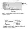
- FIG. 8shows a Monte Carlo simulation of the energy deposition heating profile for a 100 keV electron beam in silicon. If the energy is deposited rapidly compared to the thermal diffusion time constant of the system, this profile also represents the instantaneous temperature profile and thermo-elastic stress profile imparted to the system.
- M and Pcan be simultaneously adjusted to a desired combination that can result in energy or KII controlled propagation.
- electron energies of 1 MeV or lessthe general shape of the volumetric heating profile has been found to be energy independent and only scale in depth.
- FIG. 9shows the simulated E-Beam Profile with a peak temperature of 635° C. and peak position of about 5.35 um within the film. This will generate, assuming unity coupling of M and P into the crack tip, a moment M ⁇ 8 ⁇ 10 ⁇ 2 N-m/m and force P ⁇ 4.3 ⁇ 10 3 N/m. The resulting KI just exceeds 2.4 J/m 2 and KII is cancelled.
- FIG. 10shows the cleave energy contribution from each stress intensity component (KI 2 /E′ as D1 and (KII 2 /E′ as D2).
- This conditionshould allow the crack to propagate some distance until arresting. Since the crack cleave velocity is much faster than the thermal time constant of the system, this temperature profile will persist and not thermally diffuse through the cleaving process.
- E-beam spot sizes of about 500 um to a few millimetersshould extend the crack to about the same length scale. After thermal relaxation of the thermal pulse, the process can repeat to move the crack another increment.
- a CW or pulsed beamcould perform the same function in a scanning manner along the cleave tip (into the figure).
- the scanning beamcould extend the crack dynamically in synchronicity with the scanning beam. Control over depth could therefore be made by modulating the beam energy and intensity while the crack is propagating to achieve the desired depth. This suggests that reduced dose or even no dose propagation is possible using this technology.
- the E-beam technology, laser, or flashlamp technologiescould be used to detach the film from the substrate.
- the E-beam technologymay be particularly suited for this purpose, as the energy range could be adjusted to allow film temperature to rise volumetrically within the initiation area close to the edge of the substrate.
- the pulsed energywould deposit over time within the film thickness, an almost constant ⁇ T rise in temperature, with a sharp change in temperature profile adjusted located at or near to the cleave plane.
- FIG. 9Such adiabatic heating of silicon by E-beam exposure is shown in FIG. 9 , which plots energy density versus depth into silicon, for E-beam irradiation over a time period.
- the beam intensity and energyare chosen to correspond to a KII controlled propagation.
- KIIis cancelled with a peak thermal depth of 5.35 um.
- a 250 nsec pulsewould only diffuse the thermal profile by about 5 um, substantially less than the film thickness. This would generate a cleave action that would limit the presence of thermal shocks across the thickness of the film, and produce KI and KII components that can controllably cleave the film.
- the initiation cleavingcould start at an edge and be extended to cover the desired film width to support the propagation cleave method. Alternatively, the initiation cleaving could start at an interior location and then extend to the periphery. If an internal initiation cleaving is used, a vacuum environment would benefit the cleaving process by reducing the energy needed for film buckling since there will not be any appreciable pressure developing a restoring force to the upwards film movement.
- An intense thermal pulse in combination with volumetric heating characteristicscould also be used to propagate the film from the initiation region.
- a fast pulse applicationthat can heat the film thickness uniformly, could allow the controlled propagation of the film by pure shear cleaving or with a moment assist.
- the use of E-Beam technology for cleaving of filmsis described in U.S. Pat. No. 6,013,563, which is incorporated by reference in its entirety herein for all purposes.
- the E-Beam radiationmay be applied in a direction perpendicular to a face of the substrate.
- the matching of the E-beam volumetric heatingcan be made by selecting a higher or lower energy e-beam.
- the E-beam energycan be selected so that its Rp is within the thickness of the film to be cleaved in order to generate the desired moment M.
- E-beam radiationmay be particularly favored here because the energy range could be adjusted to allow a film temperature rise volumetrically within the film close to the crack tip.
- the pulsed energywould deposit within the film thickness, a sharp change in temperature profile adjusted to develop the desired M and P loading.
- a 250 nsec pulsewould only diffuse the thermal profile by about 5 um, substantially less than the film thickness. This would generate a shear cleave that would limit the presence of thermal shocks across the thickness of the film and produce a large shear that can controllably cleave the film.
- E-beam heating methodswould be beneficial in this mode, since the rapid adiabatic heating will give a sharp compressive stress profile that can help guide the propagating cleave.
- Cleave depthcould also be controlled by altering the E-beam energy, thus changing the thickness of the film that is subjected to volumetric heating.
- the heated zone widthwill dictate, to first order, the amount of crack extension that will occur upon the heating cycle. This is because after the cleave front has reached the edge of the heated cleave area, G′ will drop and the propagating cleave will arrest.
- any of the heating techniques used in conjunction with an implanted cleave layercould help use the implant induced stresses more efficiently. This would occur by the higher temperature, which would in turn increase the implant stresses (these are usually proportional to kT).
- a heated pulsecould therefore have a secondary, favorable effect on the cleave plane, enhancing stresses in the cleave plane for better guidance of cleave propagation.
- this remaining portion with a newly exposed surface regionis in condition for repeating the cleaving method by again performing the cleave initiation and propagation methods.
- a cleavage plane of lower surface energymay be selected as the surface region for the semiconductor substrate.
- a new surface planewould be substantially in the original crystallographic plane and in a good condition, with relatively small surface roughness for additional layer transfer production without need of complicated surface treatment like etching or polishing.
- the processescan be for the formation of photovoltaic cells, integrated circuits, optical devices, any combination of these, and the like.
- the type of ionic particlescan be varied from hydrogen ions to helium ions, deuterium ions, or certain combinations to allow for formation of the cleave region according to alternative embodiments.
- the cleaving processmay include temperature controlled/assisted cleaving utilizing vacuum chucking or electrostatic chucking process.
Landscapes
- Engineering & Computer Science (AREA)
- Physics & Mathematics (AREA)
- Condensed Matter Physics & Semiconductors (AREA)
- General Physics & Mathematics (AREA)
- Manufacturing & Machinery (AREA)
- Computer Hardware Design (AREA)
- Microelectronics & Electronic Packaging (AREA)
- Power Engineering (AREA)
- Crystals, And After-Treatments Of Crystals (AREA)
- Recrystallisation Techniques (AREA)
- Processing Of Stones Or Stones Resemblance Materials (AREA)
- Photovoltaic Devices (AREA)
Abstract
Description
γ′=αH2*γ (1)
where αHis a factor between 0 and 1 that serves to quantify the reduction in cleave energy due to hydrogen embrittlement. The αHterm accounts for all of the effects necessary to yield an accurate representation of all of the stress and bond damage effects. αHis experimentally determined as a function of cleave energy, dose, implant thermal conditions, and post-implant thermal conditions.
G′=2*γ′=2*αH2*γ (2)
where E′=the plane strain equation defined as E′=E/(1−ν2), and, for all purposes of this document, G is G′ and generally related to the cleave plane by equation (2):
G′=2*γ′=2*αH2*γ (2)
Where Pnand Mnare the forces and moments respectively, acting on each of the members.
where the parameters are derived from the forces, moments and geometry as described in detail by Hutchinson and Suo, “Mixed Mode Cracking in Layered Materials”, Advances in Applied Mechanics, Vol. 29 (1992), which is incorporated by reference in its entirety herein for all purposes.
P=−σhc/2
M=+σ(hhc/4−hc2/6)
The KI and KII functions (with small cross-terms ignored) is:
σ=sqrt(kTφ)*αH*K0 (11)
where
where
kT=Boltzmann's constant*absolute cleave plane temperature; and
φ=Hydrogen dose
where the cleave plane is located within a hydrogen cleave plane of peak stress σ and characteristic width hc, and has external energy added to the system in the form of a force P and moment M. These serve to modify the cleave energy and stress intensity.
M=0 andP=−σth*h.
Recognizing that a thermal stress function of magnitude αCTEE ΔT is developed by a temperature change in a material with a coefficient of thermal expansion αCTE, the equation becomes,
P=−αCTEEhΔT (14)
Where ΔT is the temperature difference between the film being subjected to thermal treatment and connected material.
where ΔT is the temperature difference imparted by the material above the cleave front and the rest of the substrate. Since the heating source adds to KII, this is predominantly KII shear cleaving.
G′=2*γ′=½*αCTE2*E*h*ΔT2*(1−ν2) (17)
Claims (34)
Priority Applications (4)
| Application Number | Priority Date | Filing Date | Title |
|---|---|---|---|
| US12/460,898US8293619B2 (en) | 2008-08-28 | 2009-07-24 | Layer transfer of films utilizing controlled propagation |
| US13/225,172US8993410B2 (en) | 2006-09-08 | 2011-09-02 | Substrate cleaving under controlled stress conditions |
| US14/618,940US9356181B2 (en) | 2006-09-08 | 2015-02-10 | Substrate cleaving under controlled stress conditions |
| US15/167,291US9640711B2 (en) | 2006-09-08 | 2016-05-27 | Substrate cleaving under controlled stress conditions |
Applications Claiming Priority (2)
| Application Number | Priority Date | Filing Date | Title |
|---|---|---|---|
| US9268308P | 2008-08-28 | 2008-08-28 | |
| US12/460,898US8293619B2 (en) | 2008-08-28 | 2009-07-24 | Layer transfer of films utilizing controlled propagation |
Related Parent Applications (1)
| Application Number | Title | Priority Date | Filing Date |
|---|---|---|---|
| US12/435,230Continuation-In-PartUS9362439B2 (en) | 2006-09-08 | 2009-05-04 | Layer transfer of films utilizing controlled shear region |
Related Child Applications (2)
| Application Number | Title | Priority Date | Filing Date |
|---|---|---|---|
| US12/730,113Continuation-In-PartUS8110480B2 (en) | 2006-09-08 | 2010-03-23 | Method and structure for fabricating solar cells using a thick layer transfer process |
| US13/225,172Continuation-In-PartUS8993410B2 (en) | 2006-09-08 | 2011-09-02 | Substrate cleaving under controlled stress conditions |
Publications (2)
| Publication Number | Publication Date |
|---|---|
| US20100055874A1 US20100055874A1 (en) | 2010-03-04 |
| US8293619B2true US8293619B2 (en) | 2012-10-23 |
Family
ID=41478750
Family Applications (1)
| Application Number | Title | Priority Date | Filing Date |
|---|---|---|---|
| US12/460,898Expired - Fee RelatedUS8293619B2 (en) | 2006-09-08 | 2009-07-24 | Layer transfer of films utilizing controlled propagation |
Country Status (5)
| Country | Link |
|---|---|
| US (1) | US8293619B2 (en) |
| EP (1) | EP2169730A3 (en) |
| JP (1) | JP2010103488A (en) |
| KR (1) | KR20100027046A (en) |
| CN (1) | CN101969046A (en) |
Cited By (9)
| Publication number | Priority date | Publication date | Assignee | Title |
|---|---|---|---|---|
| US20130032582A1 (en)* | 2011-08-01 | 2013-02-07 | Silicon Genesis Corporation | Layer transfer of films utilizing thermal flux regime for energy controlled cleaving |
| US8518807B1 (en)* | 2012-06-22 | 2013-08-27 | International Business Machines Corporation | Radiation hardened SOI structure and method of making same |
| US20140034699A1 (en)* | 2012-08-02 | 2014-02-06 | King Abdulaziz City For Science And Technology | Method for improving quality of spalled material layers |
| US9704835B2 (en) | 2015-01-09 | 2017-07-11 | Silicon Genesis Corporation | Three dimensional integrated circuit |
| US9859458B2 (en) | 2015-06-19 | 2018-01-02 | QMAT, Inc. | Bond and release layer transfer process |
| US10049915B2 (en) | 2015-01-09 | 2018-08-14 | Silicon Genesis Corporation | Three dimensional integrated circuit |
| US10573627B2 (en) | 2015-01-09 | 2020-02-25 | Silicon Genesis Corporation | Three dimensional integrated circuit |
| US10804252B2 (en) | 2015-01-09 | 2020-10-13 | Silicon Genesis Corporation | Three dimensional integrated circuit |
| US11410984B1 (en) | 2021-10-08 | 2022-08-09 | Silicon Genesis Corporation | Three dimensional integrated circuit with lateral connection layer |
Families Citing this family (15)
| Publication number | Priority date | Publication date | Assignee | Title |
|---|---|---|---|---|
| US8993410B2 (en) | 2006-09-08 | 2015-03-31 | Silicon Genesis Corporation | Substrate cleaving under controlled stress conditions |
| CN102150278A (en)* | 2008-06-11 | 2011-08-10 | 因特瓦克公司 | Formation of solar cell-selective emitter using implant and anneal method |
| JP2012521642A (en)* | 2009-03-20 | 2012-09-13 | インテバック・インコーポレイテッド | Solar cell and manufacturing method thereof |
| US8749053B2 (en)* | 2009-06-23 | 2014-06-10 | Intevac, Inc. | Plasma grid implant system for use in solar cell fabrications |
| SG183267A1 (en)* | 2010-02-09 | 2012-09-27 | Intevac Inc | An adjustable shadow mask assembly for use in solar cell fabrications |
| RU2459691C2 (en)* | 2010-11-29 | 2012-08-27 | Юрий Георгиевич Шретер | Method of separating surface layer of semiconductor chip (versions) |
| US8524572B2 (en) | 2011-10-06 | 2013-09-03 | Micron Technology, Inc. | Methods of processing units comprising crystalline materials, and methods of forming semiconductor-on-insulator constructions |
| SG11201402177XA (en) | 2011-11-08 | 2014-06-27 | Intevac Inc | Substrate processing system and method |
| US9336989B2 (en) | 2012-02-13 | 2016-05-10 | Silicon Genesis Corporation | Method of cleaving a thin sapphire layer from a bulk material by implanting a plurality of particles and performing a controlled cleaving process |
| MY178951A (en) | 2012-12-19 | 2020-10-23 | Intevac Inc | Grid for plasma ion implant |
| US20150357193A1 (en)* | 2013-01-30 | 2015-12-10 | Fraunhofer-Ges. Zur Förderung Der Angewandten Forschung E.V. | Method for producing an epitaxial semiconductor layer |
| CN103646990A (en)* | 2013-11-28 | 2014-03-19 | 青岛蓝图文化传播有限公司市南分公司 | Cleavage method |
| JP6970109B2 (en)* | 2016-03-08 | 2021-11-24 | アリゾナ・ボード・オブ・リージェンツ・オン・ビハーフ・オブ・アリゾナ・ステイト・ユニバーシティーArizona Board of Regents on behalf of Arizona State University | Acoustic-promoted crack propagation for semiconductor wafer molding |
| FR3093859B1 (en)* | 2019-03-15 | 2021-02-12 | Soitec Silicon On Insulator | Method of transferring a useful layer onto a support substrate |
| DE102024106759A1 (en)* | 2024-03-08 | 2025-09-11 | Nexwafe Gmbh | Method for detaching a semiconductor wafer from a layer stack and method for producing a semiconductor wafer |
Citations (263)
| Publication number | Priority date | Publication date | Assignee | Title |
|---|---|---|---|---|
| DE834363C (en) | 1951-02-27 | 1952-03-20 | Zentral Werkstatt Goettingen | Method and device for the production of thin mica films |
| US2614055A (en) | 1947-05-12 | 1952-10-14 | Samica Corp | Method of treating mica |
| US3117002A (en) | 1960-02-16 | 1964-01-07 | Ampco Metal Inc | Aluminum bronze alloy having improved wear resistance by the addition of cobalt, chromium, and manganese |
| US3225820A (en) | 1962-11-01 | 1965-12-28 | Gen Precision Inc | Device for controlling temperature by heat conduction |
| US3390033A (en) | 1964-08-13 | 1968-06-25 | Rca Corp | Method of separating frit sealed parts of an electron tube |
| US3392069A (en) | 1963-07-17 | 1968-07-09 | Siemens Ag | Method for producing pure polished surfaces on semiconductor bodies |
| FR1558881A (en) | 1967-05-29 | 1969-02-28 | ||
| US3551213A (en) | 1968-09-04 | 1970-12-29 | Bell Telephone Labor Inc | Geometrically selective ion bombardment by means of the photoelectric effect |
| US3770499A (en) | 1972-02-28 | 1973-11-06 | Motorola Inc | Liquid phase deposition of thin insulating and refractory film on a substrate |
| US3786359A (en) | 1969-03-28 | 1974-01-15 | Alpha Ind Inc | Ion accelerator and ion species selector |
| US3806380A (en) | 1971-03-05 | 1974-04-23 | Hitachi Ltd | Method for hardening treatment of aluminum or aluminum-base alloy |
| US3832219A (en) | 1971-04-07 | 1974-08-27 | Atomic Energy Authority Uk | Methods of treating steel surfaces to modify their structure |
| FR2235474A1 (en) | 1973-06-28 | 1975-01-24 | Ibm | |
| US3900636A (en) | 1971-01-21 | 1975-08-19 | Gillette Co | Method of treating cutting edges |
| US3901423A (en) | 1973-11-26 | 1975-08-26 | Purdue Research Foundation | Method for fracturing crystalline materials |
| FR2261802A1 (en) | 1974-02-21 | 1975-09-19 | Devienne Fernand | |
| US3915757A (en) | 1972-08-09 | 1975-10-28 | Niels N Engel | Ion plating method and product therefrom |
| US3946334A (en) | 1973-11-14 | 1976-03-23 | Nippon Electric Company, Limited | Injection semiconductor laser device |
| US3957107A (en) | 1975-02-27 | 1976-05-18 | The United States Of America As Represented By The Secretary Of The Air Force | Thermal switch |
| US3964957A (en) | 1973-12-19 | 1976-06-22 | Monsanto Company | Apparatus for processing semiconductor wafers |
| FR2298880A1 (en) | 1975-01-22 | 1976-08-20 | Commissariat Energie Atomique | IONIC IMPLANTATION METHOD AND DEVICE |
| US3993909A (en) | 1973-03-16 | 1976-11-23 | U.S. Philips Corporation | Substrate holder for etching thin films |
| US4006340A (en) | 1973-09-28 | 1977-02-01 | Compagnie Industrielle Des Telecommunications Cit-Alcatel | Device for the rapid depositing of oxides in thin layers which adhere well to plastic supports |
| US4039416A (en) | 1975-04-21 | 1977-08-02 | White Gerald W | Gasless ion plating |
| US4053335A (en) | 1976-04-02 | 1977-10-11 | International Business Machines Corporation | Method of gettering using backside polycrystalline silicon |
| US4074139A (en) | 1976-12-27 | 1978-02-14 | Rca Corporation | Apparatus and method for maskless ion implantation |
| US4107350A (en) | 1972-08-14 | 1978-08-15 | Berg Joseph E | Method for depositing film on a substrate |
| US4108751A (en) | 1977-06-06 | 1978-08-22 | King William J | Ion beam implantation-sputtering |
| US4116751A (en) | 1975-10-08 | 1978-09-26 | Solomon Zaromb | Methods and apparatus for producing unsupported monocrystalline films of silicon and of other materials |
| US4121334A (en) | 1974-12-17 | 1978-10-24 | P. R. Mallory & Co. Inc. | Application of field-assisted bonding to the mass production of silicon type pressure transducers |
| US4170662A (en) | 1974-11-05 | 1979-10-09 | Eastman Kodak Company | Plasma plating |
| US4216906A (en) | 1976-06-21 | 1980-08-12 | Flow Research, Inc. | Method of making high velocity liquid jet |
| US4237601A (en) | 1978-10-13 | 1980-12-09 | Exxon Research & Engineering Co. | Method of cleaving semiconductor diode laser wafers |
| US4244348A (en) | 1979-09-10 | 1981-01-13 | Atlantic Richfield Company | Process for cleaving crystalline materials |
| US4252837A (en) | 1976-03-23 | 1981-02-24 | Warner-Lambert Company | Blade shields |
| US4255208A (en) | 1979-05-25 | 1981-03-10 | Ramot University Authority For Applied Research And Industrial Development Ltd. | Method of producing monocrystalline semiconductor films utilizing an intermediate water dissolvable salt layer |
| US4274004A (en) | 1979-02-02 | 1981-06-16 | Hitachi, Ltd. | Ion implanter |
| US4342631A (en) | 1980-06-16 | 1982-08-03 | Illinois Tool Works Inc. | Gasless ion plating process and apparatus |
| US4346123A (en) | 1979-08-02 | 1982-08-24 | Balzers Aktiengesellschaft | Method of depositing hard wear-resistant coatings on substrates |
| US4361600A (en) | 1981-11-12 | 1982-11-30 | General Electric Company | Method of making integrated circuits |
| US4368083A (en) | 1980-02-01 | 1983-01-11 | Commissariat A L'energie Atomique | Process for doping semiconductors |
| US4375125A (en) | 1980-03-07 | 1983-03-01 | U.S. Philips Corporation | Method of passivating pn-junction in a semiconductor device |
| FR2519437A1 (en) | 1982-01-04 | 1983-07-08 | Commissariat Energie Atomique | DEVICE FOR LIMITING AND CONTROLLING THE TEMPERATURE OF A TARGET BASED ON A SUPPORT IN A VACUUM ENCLOSURE AND RECEIVING AN ENERGY BEAM AND ITS APPLICATION TO THERMAL MEASUREMENTS |
| US4412868A (en) | 1981-12-23 | 1983-11-01 | General Electric Company | Method of making integrated circuits utilizing ion implantation and selective epitaxial growth |
| FR2529383A1 (en) | 1982-06-24 | 1983-12-30 | Commissariat Energie Atomique | MECHANICAL SCANNING TARGET HOLDER USABLE IN PARTICULAR FOR THE IMPLANTATION OF IORIS |
| US4452644A (en) | 1980-02-01 | 1984-06-05 | Commissariat A L'energie Atomique | Process for doping semiconductors |
| FR2537768A1 (en) | 1982-12-08 | 1984-06-15 | Commissariat Energie Atomique | METHOD AND DEVICE FOR OBTAINING SPATIALLY MODULATED DENSITY PARTICLE BEAMS, APPLICATION TO ION ETCHING AND IMPLANTATION |
| FR2537777A1 (en) | 1982-12-10 | 1984-06-15 | Commissariat Energie Atomique | METHOD AND DEVICE FOR IMPLANTATION OF PARTICLES IN A SOLID |
| US4468309A (en) | 1983-04-22 | 1984-08-28 | White Engineering Corporation | Method for resisting galling |
| US4471003A (en) | 1980-11-25 | 1984-09-11 | Cann Gordon L | Magnetoplasmadynamic apparatus and process for the separation and deposition of materials |
| US4486247A (en) | 1982-06-21 | 1984-12-04 | Westinghouse Electric Corp. | Wear resistant steel articles with carbon, oxygen and nitrogen implanted in the surface thereof |
| US4490190A (en) | 1981-03-13 | 1984-12-25 | Societe Anonyme Dite: Vide Et Traitement | Process for thermochemical treatments of metals by ionic bombardment |
| US4495219A (en) | 1981-10-09 | 1985-01-22 | Fujitsu Limited | Process for producing dielectric layers for semiconductor devices |
| US4500563A (en) | 1982-12-15 | 1985-02-19 | Pacific Western Systems, Inc. | Independently variably controlled pulsed R.F. plasma chemical vapor processing |
| US4530149A (en) | 1982-06-24 | 1985-07-23 | Rca Corporation | Method for fabricating a self-aligned vertical IGFET |
| FR2560426A1 (en) | 1984-02-28 | 1985-08-30 | Commissariat Energie Atomique | DEVICE FOR PRODUCING IONS OF A SPECIFIED SPECIES, USING FOR SEPARATION FROM OTHER IONS, ENERGY SELECTION, APPLICATION TO ION IMPLANTATION |
| US4539050A (en) | 1982-12-15 | 1985-09-03 | Wacker-Chemitronic Gesellschaft Fur Elektronik-Grundstoffe M.B.H. | Process for the manufacture of semiconductor wafers with a rear side having a gettering action |
| FR2563377A1 (en) | 1984-04-19 | 1985-10-25 | Commissariat Energie Atomique | METHOD FOR MANUFACTURING AN INSULATED INSULATED LAYER IN A SEMICONDUCTOR SUBSTRATE, BY ION IMPLANTATION |
| US4566403A (en) | 1985-01-30 | 1986-01-28 | Sovonics Solar Systems | Apparatus for microwave glow discharge deposition |
| US4567505A (en) | 1983-10-27 | 1986-01-28 | The Board Of Trustees Of The Leland Stanford Junior University | Heat sink and method of attaching heat sink to a semiconductor integrated circuit and the like |
| US4568563A (en) | 1983-08-02 | 1986-02-04 | Standard Telephones And Cables | Optical fibre manufacture |
| FR2575601A1 (en) | 1984-12-27 | 1986-07-04 | Commissariat Energie Atomique | Method and device for determining electrical parameters of a semiconductor layer as a function of depth |
| US4645546A (en) | 1984-07-13 | 1987-02-24 | Kabushiki Kaisha Toshiba | Semiconductor substrate |
| US4684535A (en) | 1984-03-03 | 1987-08-04 | Standard Telephones & Cables | Surface treatment of plastics material |
| US4706377A (en) | 1986-01-30 | 1987-11-17 | United Technologies Corporation | Passivation of gallium arsenide by nitrogen implantation |
| US4717683A (en) | 1986-09-23 | 1988-01-05 | Motorola Inc. | CMOS process |
| US4727047A (en) | 1980-04-10 | 1988-02-23 | Massachusetts Institute Of Technology | Method of producing sheets of crystalline material |
| US4764394A (en) | 1987-01-20 | 1988-08-16 | Wisconsin Alumni Research Foundation | Method and apparatus for plasma source ion implantation |
| US4766086A (en) | 1986-03-07 | 1988-08-23 | Kabushiki Kaisha Toshiba | Method of gettering a semiconductor device and forming an isolation region therein |
| US4837172A (en) | 1986-07-18 | 1989-06-06 | Matsushita Electric Industrial Co., Ltd. | Method for removing impurities existing in semiconductor substrate |
| US4847792A (en) | 1987-05-04 | 1989-07-11 | Texas Instruments Incorporated | Process and apparatus for detecting aberrations in production process operations |
| US4846928A (en) | 1987-08-04 | 1989-07-11 | Texas Instruments, Incorporated | Process and apparatus for detecting aberrations in production process operations |
| GB2211991A (en) | 1987-10-30 | 1989-07-12 | Atomic Energy Authority Uk | Electrical isolation of regions within semiconductor bodies |
| US4853250A (en) | 1988-05-11 | 1989-08-01 | Universite De Sherbrooke | Process of depositing particulate material on a substrate |
| US4883561A (en) | 1988-03-29 | 1989-11-28 | Bell Communications Research, Inc. | Lift-off and subsequent bonding of epitaxial films |
| US4887005A (en) | 1987-09-15 | 1989-12-12 | Rough J Kirkwood H | Multiple electrode plasma reactor power distribution system |
| US4891329A (en) | 1988-11-29 | 1990-01-02 | University Of North Carolina | Method of forming a nonsilicon semiconductor on insulator structure |
| US4894709A (en) | 1988-03-09 | 1990-01-16 | Massachusetts Institute Of Technology | Forced-convection, liquid-cooled, microchannel heat sinks |
| US4906594A (en) | 1987-06-12 | 1990-03-06 | Agency Of Industrial Science And Technology | Surface smoothing method and method of forming SOI substrate using the surface smoothing method |
| US4931405A (en) | 1988-02-08 | 1990-06-05 | Kabushiki Kaisha Toshiba | Method for manufacturing a semiconductor device and suppressing the generation of bulk microdefects near the substrate surface layer |
| US4948458A (en) | 1989-08-14 | 1990-08-14 | Lam Research Corporation | Method and apparatus for producing magnetically-coupled planar plasma |
| US4952273A (en) | 1988-09-21 | 1990-08-28 | Microscience, Inc. | Plasma generation in electron cyclotron resonance |
| US4956693A (en) | 1986-03-20 | 1990-09-11 | Hitachi, Ltd. | Semiconductor device |
| US4960073A (en) | 1988-09-19 | 1990-10-02 | Anelva Corporation | Microwave plasma treatment apparatus |
| GB2231197A (en) | 1989-03-06 | 1990-11-07 | Nordiko Ltd | Plasma apparatus electrode assembly |
| US4982090A (en) | 1988-02-05 | 1991-01-01 | Gesellschaft Fur Strahlen- Und Umweltforschung Mbh (Gsf) | Method and apparatus for the quantitative, depth differential analysis of solid samples with the use of two ion beams |
| US4983251A (en) | 1985-06-20 | 1991-01-08 | U.S. Philips Corporation | Method of manufacturing semiconductor devices |
| US4996077A (en) | 1988-10-07 | 1991-02-26 | Texas Instruments Incorporated | Distributed ECR remote plasma processing and apparatus |
| US5015353A (en) | 1987-09-30 | 1991-05-14 | The United States Of America As Represented By The Secretary Of The Navy | Method for producing substoichiometric silicon nitride of preselected proportions |
| US5034343A (en) | 1990-03-08 | 1991-07-23 | Harris Corporation | Manufacturing ultra-thin wafer using a handle wafer |
| US5070040A (en) | 1990-03-09 | 1991-12-03 | University Of Colorado Foundation, Inc. | Method and apparatus for semiconductor circuit chip cooling |
| US5082793A (en) | 1965-09-28 | 1992-01-21 | Li Chou H | Method for making solid state device utilizing ion implantation techniques |
| US5102821A (en) | 1990-12-20 | 1992-04-07 | Texas Instruments Incorporated | SOI/semiconductor heterostructure fabrication by wafer bonding of polysilicon to titanium |
| US5110748A (en) | 1991-03-28 | 1992-05-05 | Honeywell Inc. | Method for fabricating high mobility thin film transistors as integrated drivers for active matrix display |
| US5133826A (en) | 1989-03-09 | 1992-07-28 | Applied Microwave Plasma Concepts, Inc. | Electron cyclotron resonance plasma source |
| US5141878A (en) | 1990-04-02 | 1992-08-25 | At&T Bell Laboratories | Silicon photodiode for monolithic integrated circuits and method for making same |
| US5162241A (en) | 1990-07-05 | 1992-11-10 | Kabushiki Kaisha Toshiba | Method of manufacturing a semiconductor device |
| FR2681472A1 (en) | 1991-09-18 | 1993-03-19 | Commissariat Energie Atomique | PROCESS FOR PRODUCING THIN FILMS OF SEMICONDUCTOR MATERIAL |
| US5196355A (en) | 1989-04-24 | 1993-03-23 | Ibis Technology Corporation | Simox materials through energy variation |
| US5198071A (en) | 1991-11-25 | 1993-03-30 | Applied Materials, Inc. | Process for inhibiting slip and microcracking while forming epitaxial layer on semiconductor wafer |
| US5198371A (en) | 1990-09-24 | 1993-03-30 | Biota Corp. | Method of making silicon material with enhanced surface mobility by hydrogen ion implantation |
| US5202095A (en) | 1988-12-27 | 1993-04-13 | Matsushita Electric Industrial Co., Ltd. | Microwave plasma processor |
| US5203960A (en) | 1989-03-09 | 1993-04-20 | Applied Microwave Plasma Concepts, Inc. | Method of operation of electron cyclotron resonance plasma source |
| US5206749A (en) | 1990-12-31 | 1993-04-27 | Kopin Corporation | Liquid crystal display having essentially single crystal transistors pixels and driving circuits |
| US5213986A (en) | 1992-04-10 | 1993-05-25 | North American Philips Corporation | Process for making thin film silicon-on-insulator wafers employing wafer bonding and wafer thinning |
| US5213451A (en) | 1991-01-10 | 1993-05-25 | Wacker-Chemitronic Gesellschaft Fur Elektronik-Grundstoffe Mbh | Apparatus and method of automatically separating stacked wafers |
| US5234529A (en) | 1991-10-10 | 1993-08-10 | Johnson Wayne L | Plasma generating apparatus employing capacitive shielding and process for using such apparatus |
| US5234535A (en) | 1992-12-10 | 1993-08-10 | International Business Machines Corporation | Method of producing a thin silicon-on-insulator layer |
| US5242861A (en) | 1991-06-06 | 1993-09-07 | Nec Corporation | Method for manufacturing semiconductor device having a multilayer wiring structure |
| US5250328A (en) | 1991-04-30 | 1993-10-05 | Schott Glaswerke | Process and apparatus for plasma CVD coating or plasma treating substrates |
| US5252178A (en) | 1992-06-24 | 1993-10-12 | Texas Instruments Incorporated | Multi-zone plasma processing method and apparatus |
| US5256562A (en) | 1990-12-31 | 1993-10-26 | Kopin Corporation | Method for manufacturing a semiconductor device using a circuit transfer film |
| US5258325A (en) | 1990-12-31 | 1993-11-02 | Kopin Corporation | Method for manufacturing a semiconductor device using a circuit transfer film |
| US5258320A (en) | 1990-12-31 | 1993-11-02 | Kopin Corporation | Single crystal silicon arrayed devices for display panels |
| US5269880A (en) | 1992-04-03 | 1993-12-14 | Northern Telecom Limited | Tapering sidewalls of via holes |
| US5273610A (en) | 1992-06-23 | 1993-12-28 | Association Institutions For Material Sciences, Inc. | Apparatus and method for determining power in plasma processing |
| US5277748A (en) | 1992-01-31 | 1994-01-11 | Canon Kabushiki Kaisha | Semiconductor device substrate and process for preparing the same |
| EP0296804B1 (en) | 1987-06-24 | 1994-03-30 | Advanced Semiconductor Materials America, Inc. | Process for epitaxial deposition of silicone |
| US5304509A (en) | 1992-08-24 | 1994-04-19 | Midwest Research Institute | Back-side hydrogenation technique for defect passivation in silicon solar cells |
| US5303574A (en) | 1991-02-12 | 1994-04-19 | Hughes Aircraft Company | Evaluation of the extent of wear of articles |
| US5308776A (en) | 1991-02-20 | 1994-05-03 | Fujitsu Limited | Method of manufacturing SOI semiconductor device |
| US5342472A (en) | 1991-08-12 | 1994-08-30 | Tokyo Electron Limited | Plasma processing apparatus |
| US5344524A (en) | 1993-06-30 | 1994-09-06 | Honeywell Inc. | SOI substrate fabrication |
| US5354381A (en) | 1993-05-07 | 1994-10-11 | Varian Associates, Inc. | Plasma immersion ion implantation (PI3) apparatus |
| US5362671A (en) | 1990-12-31 | 1994-11-08 | Kopin Corporation | Method of fabricating single crystal silicon arrayed devices for display panels |
| US5363603A (en) | 1992-06-22 | 1994-11-15 | Alliant Techsystems, Inc. | Abrasive fluid jet cutting compositon and method |
| US5368710A (en) | 1992-05-14 | 1994-11-29 | Lam Research Corporation | Method of treating an article with a plasma apparatus in which a uniform electric field is induced by a dielectric window |
| US5370765A (en) | 1989-03-09 | 1994-12-06 | Applied Microwave Plasma Concepts, Inc. | Electron cyclotron resonance plasma source and method of operation |
| US5376560A (en) | 1992-04-03 | 1994-12-27 | National Semiconductor Corporation | Method for forming isolated semiconductor structures |
| US5404079A (en) | 1992-08-13 | 1995-04-04 | Matsushita Electric Industrial Co., Ltd. | Plasma generating apparatus |
| US5403434A (en) | 1994-01-06 | 1995-04-04 | Texas Instruments Incorporated | Low-temperature in-situ dry cleaning process for semiconductor wafer |
| US5405480A (en) | 1992-11-04 | 1995-04-11 | Novellus Systems, Inc. | Induction plasma source |
| WO1995010718A1 (en) | 1993-10-13 | 1995-04-20 | Zexel Torsen Inc. | Differential with friction-enhancing wedge |
| US5409563A (en) | 1993-02-26 | 1995-04-25 | Micron Technology, Inc. | Method for etching high aspect ratio features |
| US5411592A (en) | 1994-06-06 | 1995-05-02 | Ovonic Battery Company, Inc. | Apparatus for deposition of thin-film, solid state batteries |
| US5413679A (en) | 1993-06-30 | 1995-05-09 | The United States Of America As Represented By The Secretary Of The Navy | Method of producing a silicon membrane using a silicon alloy etch stop layer |
| US5427052A (en) | 1991-04-27 | 1995-06-27 | Shin-Etsu Handotai Co., Ltd. | Method and apparatus for production of extremely thin SOI film substrate |
| FR2714524A1 (en) | 1993-12-23 | 1995-06-30 | Commissariat Energie Atomique | Method of producing a relief structure on a support made of semiconductor material |
| US5435880A (en) | 1992-10-14 | 1995-07-25 | Tokyo Ohka Kogyo Co., Ltd. | Plasma processing apparatus |
| FR2715501A1 (en) | 1994-01-26 | 1995-07-28 | Commissariat Energie Atomique | Process for depositing semiconductor blades on a support |
| FR2715502A1 (en) | 1994-01-26 | 1995-07-28 | Commissariat Energie Atomique | Structure having cavities and method for producing such a structure |
| US5444557A (en) | 1990-12-31 | 1995-08-22 | Kopin Corporation | Single crystal silicon arrayed devices for projection displays |
| US5443661A (en) | 1993-07-27 | 1995-08-22 | Nec Corporation | SOI (silicon on insulator) substrate with enhanced gettering effects |
| US5459016A (en) | 1993-12-16 | 1995-10-17 | Minnesota Mining And Manufacturing Company | Nanostructured thermal transfer donor element |
| WO1995031825A1 (en) | 1994-05-18 | 1995-11-23 | Commissariat A L'energie Atomique | Method for production of a structure with a low level of dislocations and having an oxide layer buried in a semiconductor substrate |
| US5475514A (en) | 1990-12-31 | 1995-12-12 | Kopin Corporation | Transferred single crystal arrayed devices including a light shield for projection displays |
| US5476691A (en) | 1994-01-21 | 1995-12-19 | International Business Machines, Inc. | Surface treatment of magnetic recording heads |
| US5480842A (en) | 1994-04-11 | 1996-01-02 | At&T Corp. | Method for fabricating thin, strong, and flexible die for smart cards |
| US5487785A (en) | 1993-03-26 | 1996-01-30 | Tokyo Electron Kabushiki Kaisha | Plasma treatment apparatus |
| FR2725074A1 (en) | 1994-09-22 | 1996-03-29 | Commissariat Energie Atomique | PROCESS FOR MANUFACTURING A STRUCTURE INCLUDING A THIN SEMICONDUCTOR LAYER ON A SUBSTRATE |
| US5504328A (en) | 1994-12-09 | 1996-04-02 | Sematech, Inc. | Endpoint detection utilizing ultraviolet mass spectrometry |
| FR2715503B1 (en) | 1994-01-26 | 1996-04-05 | Commissariat Energie Atomique | Substrate for integrated components comprising a thin layer and its production method. |
| US5506176A (en) | 1992-12-07 | 1996-04-09 | Sony Corporation | Method of making a semiconductor device having a process of hydrogen annealing |
| US5508207A (en) | 1992-06-29 | 1996-04-16 | Sumitomo Sitix Corporation | Method of annealing a semiconductor wafer in a hydrogen atmosphere to desorb surface contaminants |
| US5514235A (en) | 1993-06-29 | 1996-05-07 | Shin-Etsu Handotai Co., Ltd. | Method of making bonded wafers |
| US5518965A (en) | 1993-07-09 | 1996-05-21 | France Telecom | Process for producing a structure integrating a cleaved optical guide with an optical fibre support for a guide-fibre optical coupling |
| US5528397A (en) | 1991-12-03 | 1996-06-18 | Kopin Corporation | Single crystal silicon transistors for display panels |
| US5539245A (en) | 1991-11-18 | 1996-07-23 | Mitsubishi Materials Silicon Corporation | Semiconductor substrate having a gettering layer |
| US5558718A (en) | 1994-04-08 | 1996-09-24 | The Regents, University Of California | Pulsed source ion implantation apparatus and method |
| US5569620A (en) | 1992-09-03 | 1996-10-29 | Harris Corporation | Bonded wafer processing with metal silicidation |
| US5581385A (en) | 1990-12-31 | 1996-12-03 | Kopin Corporation | Single crystal silicon arrayed devices for projection displays |
| US5585304A (en) | 1991-06-13 | 1996-12-17 | Agency Industrial Science | Method of making semiconductor device with multiple transparent layers |
| US5611855A (en) | 1995-01-31 | 1997-03-18 | Seh America, Inc. | Method for manufacturing a calibration wafer having a microdefect-free layer of a precisely predetermined depth |
| US5643834A (en) | 1991-07-01 | 1997-07-01 | Sumitomo Electric Industries, Ltd. | Process for manufacturing a semiconductor substrate comprising laminated copper, silicon oxide and silicon nitride layers |
| US5653811A (en) | 1995-07-19 | 1997-08-05 | Chan; Chung | System for the plasma treatment of large area substrates |
| US5686980A (en) | 1995-04-03 | 1997-11-11 | Kabushiki Kaisha Toshiba | Light-shielding film, useable in an LCD, in which fine particles of a metal or semi-metal are dispersed in and throughout an inorganic insulating film |
| US5700333A (en) | 1995-03-27 | 1997-12-23 | Semiconductor Energy Laboratory Co., Ltd. | Thin-film photoelectric conversion device and a method of manufacturing the same |
| US5705421A (en) | 1994-11-24 | 1998-01-06 | Sony Corporation | A SOI substrate fabricating method |
| US5710057A (en) | 1996-07-12 | 1998-01-20 | Kenney; Donald M. | SOI fabrication method |
| US5714395A (en) | 1995-09-13 | 1998-02-03 | Commissariat A L'energie Atomique | Process for the manufacture of thin films of semiconductor material |
| US5744852A (en) | 1995-05-17 | 1998-04-28 | Harris Corporation | Bonded wafer |
| US5753560A (en) | 1996-10-31 | 1998-05-19 | Motorola, Inc. | Method for fabricating a semiconductor device using lateral gettering |
| US5755914A (en) | 1992-08-25 | 1998-05-26 | Canon Kabushiki Kaisha | Method for bonding semiconductor substrates |
| US5763319A (en) | 1995-08-14 | 1998-06-09 | Advanced Materials Engineering | Process for fabricating semiconductor devices with shallowly doped regions using dopant compounds containing elements of high solid solubility |
| US5783022A (en) | 1995-10-31 | 1998-07-21 | Samsung Electronics Co., Ltd. | Apparatus and methods for wafer debonding using a liquid jet |
| US5793913A (en) | 1996-07-10 | 1998-08-11 | Northern Telecom Limited | Method for the hybrid integration of discrete elements on a semiconductor substrate |
| US5811348A (en) | 1995-02-02 | 1998-09-22 | Sony Corporation | Method for separating a device-forming layer from a base body |
| DE19753494A1 (en) | 1997-03-31 | 1998-10-01 | Mitsubishi Electric Corp | Silicon wafer especially SOI wafer production |
| US5821158A (en) | 1995-08-28 | 1998-10-13 | Nec Corporation | Substrate surface treatment method capable of removing a spontaneous oxide film at a relatively low temperature |
| US5824595A (en) | 1995-10-17 | 1998-10-20 | Deutsche Itt Industries Gmbh | Method of separating electronic elements |
| US5827751A (en) | 1991-12-06 | 1998-10-27 | Picogiga Societe Anonyme | Method of making semiconductor components, in particular on GaAs of InP, with the substrate being recovered chemically |
| US5841931A (en) | 1996-11-26 | 1998-11-24 | Massachusetts Institute Of Technology | Methods of forming polycrystalline semiconductor waveguides for optoelectronic integrated circuits, and devices formed thereby |
| US5840590A (en) | 1993-12-01 | 1998-11-24 | Sandia Corporation | Impurity gettering in silicon using cavities formed by helium implantation and annealing |
| US5854123A (en) | 1995-10-06 | 1998-12-29 | Canon Kabushiki Kaisha | Method for producing semiconductor substrate |
| US5869405A (en) | 1996-01-03 | 1999-02-09 | Micron Technology, Inc. | In situ rapid thermal etch and rapid thermal oxidation |
| US5869387A (en) | 1992-01-30 | 1999-02-09 | Canon Kabushiki Kaisha | Process for producing semiconductor substrate by heating to flatten an unpolished surface |
| US5877070A (en) | 1997-05-31 | 1999-03-02 | Max-Planck Society | Method for the transfer of thin layers of monocrystalline material to a desirable substrate |
| US5882987A (en) | 1997-08-26 | 1999-03-16 | International Business Machines Corporation | Smart-cut process for the production of thin semiconductor material films |
| EP0905767A1 (en) | 1997-09-26 | 1999-03-31 | Shin-Etsu Handotai Company Limited | Method of fabricating an SOI wafer and SOI wafer fabricated thereby |
| US5897743A (en) | 1996-01-22 | 1999-04-27 | Komatsu Electronic Metals Co., Ltd. | Jig for peeling a bonded wafer |
| US5906951A (en) | 1997-04-30 | 1999-05-25 | International Business Machines Corporation | Strained Si/SiGe layers on insulator |
| US5909627A (en) | 1998-05-18 | 1999-06-01 | Philips Electronics North America Corporation | Process for production of thin layers of semiconductor material |
| JP2901031B2 (en) | 1992-01-30 | 1999-06-02 | キヤノン株式会社 | Semiconductor substrate and method of manufacturing the same |
| JP2910001B2 (en) | 1992-01-30 | 1999-06-23 | キヤノン株式会社 | Semiconductor substrate and method of manufacturing the same |
| US5920764A (en) | 1997-09-30 | 1999-07-06 | International Business Machines Corporation | Process for restoring rejected wafers in line for reuse as new |
| WO1999035674A1 (en) | 1997-12-30 | 1999-07-15 | Commissariat A L'energie Atomique | Method for transferring a thin film comprising a step of generating inclusions |
| US5942050A (en) | 1994-12-02 | 1999-08-24 | Pacific Solar Pty Ltd. | Method of manufacturing a multilayer solar cell |
| US5953622A (en) | 1996-11-23 | 1999-09-14 | Hyundai Electronics Industries Co., Ltd. | Method for fabricating semiconductor wafers |
| US5966625A (en) | 1995-03-20 | 1999-10-12 | Toshiba Ceramics Co., Ltd. | Method for making a slant-surface silicon wafer having a reconstructed atomic-level stepped surface structure |
| US5966620A (en) | 1996-11-15 | 1999-10-12 | Canon Kabshiki Kaisha | Process for producing semiconductor article |
| US5968279A (en) | 1997-06-13 | 1999-10-19 | Mattson Technology, Inc. | Method of cleaning wafer substrates |
| US5985742A (en) | 1997-05-12 | 1999-11-16 | Silicon Genesis Corporation | Controlled cleavage process and device for patterned films |
| US5993677A (en) | 1996-01-25 | 1999-11-30 | Commissariat A L'energie Atomique | Process for transferring a thin film from an initial substrate onto a final substrate |
| US6004868A (en) | 1996-01-17 | 1999-12-21 | Micron Technology, Inc. | Method for CMOS well drive in a non-inert ambient |
| US6008128A (en) | 1997-07-18 | 1999-12-28 | Shin-Etsu Handotai Co., Ltd. | Method for smoothing surface of silicon single crystal substrate |
| EP0971395A1 (en) | 1998-07-07 | 2000-01-12 | Shin-Etsu Handotai Company Limited | "A method of fabricating an SOI wafer and SOI wafer fabricated by the method" |
| US6020252A (en) | 1996-05-15 | 2000-02-01 | Commissariat A L'energie Atomique | Method of producing a thin layer of semiconductor material |
| US6027988A (en) | 1997-05-28 | 2000-02-22 | The Regents Of The University Of California | Method of separating films from bulk substrates by plasma immersion ion implantation |
| US6033974A (en) | 1997-05-12 | 2000-03-07 | Silicon Genesis Corporation | Method for controlled cleaving process |
| US6066915A (en) | 1997-03-28 | 2000-05-23 | Pixtech Sa | Spacer arrangement in a flat display screen |
| US6077383A (en) | 1996-08-12 | 2000-06-20 | Commissariat A L'energie | Device for separating wafers and process for using said device |
| US6083324A (en) | 1998-02-19 | 2000-07-04 | Silicon Genesis Corporation | Gettering technique for silicon-on-insulator wafers |
| US6103599A (en) | 1997-07-25 | 2000-08-15 | Silicon Genesis Corporation | Planarizing technique for multilayered substrates |
| US6107653A (en) | 1997-06-24 | 2000-08-22 | Massachusetts Institute Of Technology | Controlling threading dislocation densities in Ge on Si using graded GeSi layers and planarization |
| US6107213A (en) | 1996-02-01 | 2000-08-22 | Sony Corporation | Method for making thin film semiconductor |
| US6120597A (en) | 1998-02-17 | 2000-09-19 | The Trustees Of Columbia University In The City Of New York | Crystal ion-slicing of single-crystal films |
| US6143628A (en) | 1997-03-27 | 2000-11-07 | Canon Kabushiki Kaisha | Semiconductor substrate and method of manufacturing the same |
| US6150239A (en) | 1997-05-31 | 2000-11-21 | Max Planck Society | Method for the transfer of thin layers monocrystalline material onto a desirable substrate |
| US6171982B1 (en) | 1997-12-26 | 2001-01-09 | Canon Kabushiki Kaisha | Method and apparatus for heat-treating an SOI substrate and method of preparing an SOI substrate by using the same |
| US6171965B1 (en) | 1999-04-21 | 2001-01-09 | Silicon Genesis Corporation | Treatment method of cleaved film for the manufacture of substrates |
| US6184111B1 (en) | 1998-06-23 | 2001-02-06 | Silicon Genesis Corporation | Pre-semiconductor process implant and post-process film separation |
| US6190998B1 (en) | 1996-05-15 | 2001-02-20 | Commissariat A L'energie Atomique | Method for achieving a thin film of solid material and applications of this method |
| US6191007B1 (en) | 1997-04-28 | 2001-02-20 | Denso Corporation | Method for manufacturing a semiconductor substrate |
| US6204151B1 (en) | 1999-04-21 | 2001-03-20 | Silicon Genesis Corporation | Smoothing method for cleaved films made using thermal treatment |
| US6214701B1 (en) | 1997-12-26 | 2001-04-10 | Sony Corporation | Semiconductor substrate and thin film semiconductor device, method of manufacturing the same, and anodizing apparatus |
| US6251754B1 (en) | 1997-05-09 | 2001-06-26 | Denso Corporation | Semiconductor substrate manufacturing method |
| US6263941B1 (en) | 1999-08-10 | 2001-07-24 | Silicon Genesis Corporation | Nozzle for cleaving substrates |
| US6274464B2 (en) | 1998-02-06 | 2001-08-14 | Texas Instruments Incorporated | Epitaxial cleaning process using HCL and N-type dopant gas to reduce defect density and auto doping effects |
| US6287941B1 (en) | 1999-04-21 | 2001-09-11 | Silicon Genesis Corporation | Surface finishing of SOI substrates using an EPI process |
| US6294478B1 (en) | 1996-02-28 | 2001-09-25 | Canon Kabushiki Kaisha | Fabrication process for a semiconductor substrate |
| US20010039095A1 (en) | 2000-01-21 | 2001-11-08 | Michel Marty | Process for producing a bipolar transistor with self-aligned emitter and extrinsic base |
| US6335269B1 (en) | 1998-09-04 | 2002-01-01 | Canon Kabushiki Kaisha | Semiconductor substrate and method for producing the same |
| US6342436B1 (en) | 1998-01-04 | 2002-01-29 | Sony Corporation | Method of manufacturing semiconductor substrate and method of manufacturing solid-state image-pickup device |
| US6376806B2 (en) | 2000-05-09 | 2002-04-23 | Woo Sik Yoo | Flash anneal |
| US6452091B1 (en) | 1999-07-14 | 2002-09-17 | Canon Kabushiki Kaisha | Method of producing thin-film single-crystal device, solar cell module and method of producing the same |
| US6455397B1 (en) | 1999-11-16 | 2002-09-24 | Rona E. Belford | Method of producing strained microelectronic and/or optical integrated and discrete devices |
| US20020174828A1 (en) | 2001-03-30 | 2002-11-28 | Memc Electronic Materials, Inc. | Thermal annealing process for producing silicon wafers with improved surface characteristics |
| US6503773B2 (en) | 2000-01-20 | 2003-01-07 | Amberwave Systems Corporation | Low threading dislocation density relaxed mismatched epilayers without high temperature growth |
| US6514836B2 (en) | 2001-06-04 | 2003-02-04 | Rona Elizabeth Belford | Methods of producing strained microelectronic and/or optical integrated and discrete devices |
| US6534381B2 (en) | 1999-01-08 | 2003-03-18 | Silicon Genesis Corporation | Method for fabricating multi-layered substrates |
| US20030077885A1 (en) | 2000-05-30 | 2003-04-24 | Bernard Aspar | Embrittled substrate and method for making same |
| US6563152B2 (en) | 2000-12-29 | 2003-05-13 | Intel Corporation | Technique to obtain high mobility channels in MOS transistors by forming a strain layer on an underside of a channel |
| US20030096098A1 (en) | 2001-10-05 | 2003-05-22 | Ovshinsky Stanford R. | Semiconductor with coordinatively irregular structures |
| US20030140844A1 (en) | 2002-01-31 | 2003-07-31 | Maa Jer-Shen | Method to form thick relaxed SiGe Layer with trench structure |
| US6621131B2 (en) | 2001-11-01 | 2003-09-16 | Intel Corporation | Semiconductor transistor having a stressed channel |
| US20030186493A1 (en) | 2000-04-03 | 2003-10-02 | Atsushi Iwasaki | Method and device for making substrates |
| US20030216008A1 (en)* | 2002-05-02 | 2003-11-20 | Walter Schwarzenbach | Process for dataching layers of material |
| US6723661B2 (en) | 2001-03-02 | 2004-04-20 | Amberwave Systems Corporation | Relaxed silicon germanium platform for high speed CMOS electronics and high speed analog circuits |
| EP1085562A3 (en) | 1999-09-17 | 2004-06-09 | Applied Materials, Inc. | Apparatus and method for surface finishing a silicon film |
| US20040188487A1 (en)* | 2001-08-07 | 2004-09-30 | Thierry Barge | Apparatus and method for splitting substrates |
| US20040253794A1 (en) | 2001-05-18 | 2004-12-16 | Faris Sadeg M. | MEMS and method of manufacturing MEMS |
| US6858107B2 (en) | 2002-07-17 | 2005-02-22 | S.O.I. Tec Silicon On Insulator Technologies S.A. | Method of fabricating substrates, in particular for optics, electronics or optoelectronics |
| US6884697B2 (en)* | 2002-01-16 | 2005-04-26 | S.O.I.Tech Silicon On Insulator Technologies S.A. | Process for cleaving a wafer layer from a donor wafer |
| US20050118754A1 (en) | 2003-11-18 | 2005-06-02 | Silicon Genesis Corporation | Method for fabricating semiconductor devices using strained silicon bearing material |
| US6911376B2 (en) | 2003-10-01 | 2005-06-28 | Wafermasters | Selective heating using flash anneal |
| US20050189013A1 (en) | 2003-12-23 | 2005-09-01 | Oliver Hartley | Process for manufacturing photovoltaic cells |
| US20060014366A1 (en) | 2002-06-07 | 2006-01-19 | Amberwave Systems Corporation | Control of strain in device layers by prevention of relaxation |
| US20060030122A1 (en) | 1996-08-27 | 2006-02-09 | Seiko Epson Corporation | Exfoliating method, transferring method of thin film device, and thin film device, thin film integrated circuit device, and liquid crystal display device produced by the same |
| US20060038182A1 (en) | 2004-06-04 | 2006-02-23 | The Board Of Trustees Of The University | Stretchable semiconductor elements and stretchable electrical circuits |
| US7019339B2 (en) | 2001-04-17 | 2006-03-28 | California Institute Of Technology | Method of using a germanium layer transfer to Si for photovoltaic applications and heterostructure made thereby |
| US20070122926A1 (en)* | 2001-04-10 | 2007-05-31 | S.O.I.Tec Silicon On Insulator Technologies S.A. | Substrate layer cutting device and method |
| JP4076503B2 (en) | 2002-02-26 | 2008-04-16 | エボニック デグサ ゲーエムベーハー | CERAMIC MEMBRANE BASED ON SUPPORT WITH POLYMER FIBERS, PROCESS FOR PRODUCTION AND USE |
| US7825002B2 (en)* | 2001-08-22 | 2010-11-02 | Semiconductor Energy Laboratory Co., Ltd. | Method of peeling thin film device and method of manufacturing semiconductor device using peeled thin film device |
Family Cites Families (6)
| Publication number | Priority date | Publication date | Assignee | Title |
|---|---|---|---|---|
| WO1998052216A1 (en)* | 1997-05-12 | 1998-11-19 | Silicon Genesis Corporation | A controlled cleavage process |
| AU6905000A (en)* | 1999-08-10 | 2001-03-05 | Silicon Genesis Corporation | A cleaving process to fabricate multilayered substrates using low implantation doses |
| FR2811807B1 (en)* | 2000-07-12 | 2003-07-04 | Commissariat Energie Atomique | METHOD OF CUTTING A BLOCK OF MATERIAL AND FORMING A THIN FILM |
| JP2004140266A (en)* | 2002-10-18 | 2004-05-13 | Ishikawajima Harima Heavy Ind Co Ltd | Thin film layer wafer manufacturing method and thin film layer wafer |
| WO2006093817A2 (en)* | 2005-02-28 | 2006-09-08 | Silicon Genesis Corporation | Substrate stiffness method and resulting devices |
| US7811900B2 (en)* | 2006-09-08 | 2010-10-12 | Silicon Genesis Corporation | Method and structure for fabricating solar cells using a thick layer transfer process |
- 2009
- 2009-07-24USUS12/460,898patent/US8293619B2/ennot_activeExpired - Fee Related
- 2009-08-25JPJP2009194807Apatent/JP2010103488A/enactivePending
- 2009-08-27CNCN2009102530270Apatent/CN101969046A/enactivePending
- 2009-08-27EPEP09275067.8Apatent/EP2169730A3/ennot_activeWithdrawn
- 2009-08-28KRKR1020090080240Apatent/KR20100027046A/ennot_activeCeased
Patent Citations (297)
| Publication number | Priority date | Publication date | Assignee | Title |
|---|---|---|---|---|
| US2614055A (en) | 1947-05-12 | 1952-10-14 | Samica Corp | Method of treating mica |
| DE834363C (en) | 1951-02-27 | 1952-03-20 | Zentral Werkstatt Goettingen | Method and device for the production of thin mica films |
| US3117002A (en) | 1960-02-16 | 1964-01-07 | Ampco Metal Inc | Aluminum bronze alloy having improved wear resistance by the addition of cobalt, chromium, and manganese |
| US3225820A (en) | 1962-11-01 | 1965-12-28 | Gen Precision Inc | Device for controlling temperature by heat conduction |
| US3392069A (en) | 1963-07-17 | 1968-07-09 | Siemens Ag | Method for producing pure polished surfaces on semiconductor bodies |
| US3390033A (en) | 1964-08-13 | 1968-06-25 | Rca Corp | Method of separating frit sealed parts of an electron tube |
| US5082793A (en) | 1965-09-28 | 1992-01-21 | Li Chou H | Method for making solid state device utilizing ion implantation techniques |
| FR1558881A (en) | 1967-05-29 | 1969-02-28 | ||
| US3551213A (en) | 1968-09-04 | 1970-12-29 | Bell Telephone Labor Inc | Geometrically selective ion bombardment by means of the photoelectric effect |
| US3786359A (en) | 1969-03-28 | 1974-01-15 | Alpha Ind Inc | Ion accelerator and ion species selector |
| US3900636A (en) | 1971-01-21 | 1975-08-19 | Gillette Co | Method of treating cutting edges |
| US3806380A (en) | 1971-03-05 | 1974-04-23 | Hitachi Ltd | Method for hardening treatment of aluminum or aluminum-base alloy |
| US3832219A (en) | 1971-04-07 | 1974-08-27 | Atomic Energy Authority Uk | Methods of treating steel surfaces to modify their structure |
| US3770499A (en) | 1972-02-28 | 1973-11-06 | Motorola Inc | Liquid phase deposition of thin insulating and refractory film on a substrate |
| US3915757A (en) | 1972-08-09 | 1975-10-28 | Niels N Engel | Ion plating method and product therefrom |
| US4107350A (en) | 1972-08-14 | 1978-08-15 | Berg Joseph E | Method for depositing film on a substrate |
| US3993909A (en) | 1973-03-16 | 1976-11-23 | U.S. Philips Corporation | Substrate holder for etching thin films |
| FR2235474A1 (en) | 1973-06-28 | 1975-01-24 | Ibm | |
| US4006340A (en) | 1973-09-28 | 1977-02-01 | Compagnie Industrielle Des Telecommunications Cit-Alcatel | Device for the rapid depositing of oxides in thin layers which adhere well to plastic supports |
| US3946334A (en) | 1973-11-14 | 1976-03-23 | Nippon Electric Company, Limited | Injection semiconductor laser device |
| US3901423A (en) | 1973-11-26 | 1975-08-26 | Purdue Research Foundation | Method for fracturing crystalline materials |
| US3964957A (en) | 1973-12-19 | 1976-06-22 | Monsanto Company | Apparatus for processing semiconductor wafers |
| FR2261802A1 (en) | 1974-02-21 | 1975-09-19 | Devienne Fernand | |
| US4170662A (en) | 1974-11-05 | 1979-10-09 | Eastman Kodak Company | Plasma plating |
| US4121334A (en) | 1974-12-17 | 1978-10-24 | P. R. Mallory & Co. Inc. | Application of field-assisted bonding to the mass production of silicon type pressure transducers |
| FR2298880A1 (en) | 1975-01-22 | 1976-08-20 | Commissariat Energie Atomique | IONIC IMPLANTATION METHOD AND DEVICE |
| US3957107A (en) | 1975-02-27 | 1976-05-18 | The United States Of America As Represented By The Secretary Of The Air Force | Thermal switch |
| US4039416A (en) | 1975-04-21 | 1977-08-02 | White Gerald W | Gasless ion plating |
| US4116751A (en) | 1975-10-08 | 1978-09-26 | Solomon Zaromb | Methods and apparatus for producing unsupported monocrystalline films of silicon and of other materials |
| US4252837A (en) | 1976-03-23 | 1981-02-24 | Warner-Lambert Company | Blade shields |
| US4053335A (en) | 1976-04-02 | 1977-10-11 | International Business Machines Corporation | Method of gettering using backside polycrystalline silicon |
| US4216906A (en) | 1976-06-21 | 1980-08-12 | Flow Research, Inc. | Method of making high velocity liquid jet |
| US4074139A (en) | 1976-12-27 | 1978-02-14 | Rca Corporation | Apparatus and method for maskless ion implantation |
| US4108751A (en) | 1977-06-06 | 1978-08-22 | King William J | Ion beam implantation-sputtering |
| US4237601A (en) | 1978-10-13 | 1980-12-09 | Exxon Research & Engineering Co. | Method of cleaving semiconductor diode laser wafers |
| US4274004A (en) | 1979-02-02 | 1981-06-16 | Hitachi, Ltd. | Ion implanter |
| US4255208A (en) | 1979-05-25 | 1981-03-10 | Ramot University Authority For Applied Research And Industrial Development Ltd. | Method of producing monocrystalline semiconductor films utilizing an intermediate water dissolvable salt layer |
| US4346123A (en) | 1979-08-02 | 1982-08-24 | Balzers Aktiengesellschaft | Method of depositing hard wear-resistant coatings on substrates |
| US4244348A (en) | 1979-09-10 | 1981-01-13 | Atlantic Richfield Company | Process for cleaving crystalline materials |
| US4368083A (en) | 1980-02-01 | 1983-01-11 | Commissariat A L'energie Atomique | Process for doping semiconductors |
| US4452644A (en) | 1980-02-01 | 1984-06-05 | Commissariat A L'energie Atomique | Process for doping semiconductors |
| US4375125A (en) | 1980-03-07 | 1983-03-01 | U.S. Philips Corporation | Method of passivating pn-junction in a semiconductor device |
| US4727047A (en) | 1980-04-10 | 1988-02-23 | Massachusetts Institute Of Technology | Method of producing sheets of crystalline material |
| US4342631A (en) | 1980-06-16 | 1982-08-03 | Illinois Tool Works Inc. | Gasless ion plating process and apparatus |
| US4471003A (en) | 1980-11-25 | 1984-09-11 | Cann Gordon L | Magnetoplasmadynamic apparatus and process for the separation and deposition of materials |
| US4490190A (en) | 1981-03-13 | 1984-12-25 | Societe Anonyme Dite: Vide Et Traitement | Process for thermochemical treatments of metals by ionic bombardment |
| US4495219A (en) | 1981-10-09 | 1985-01-22 | Fujitsu Limited | Process for producing dielectric layers for semiconductor devices |
| US4361600A (en) | 1981-11-12 | 1982-11-30 | General Electric Company | Method of making integrated circuits |
| US4412868A (en) | 1981-12-23 | 1983-11-01 | General Electric Company | Method of making integrated circuits utilizing ion implantation and selective epitaxial growth |
| FR2519437A1 (en) | 1982-01-04 | 1983-07-08 | Commissariat Energie Atomique | DEVICE FOR LIMITING AND CONTROLLING THE TEMPERATURE OF A TARGET BASED ON A SUPPORT IN A VACUUM ENCLOSURE AND RECEIVING AN ENERGY BEAM AND ITS APPLICATION TO THERMAL MEASUREMENTS |
| US4486247A (en) | 1982-06-21 | 1984-12-04 | Westinghouse Electric Corp. | Wear resistant steel articles with carbon, oxygen and nitrogen implanted in the surface thereof |
| US4508056A (en) | 1982-06-24 | 1985-04-02 | Commissariat A L'energie Atomique | Target holder with mechanical scanning |
| FR2529383A1 (en) | 1982-06-24 | 1983-12-30 | Commissariat Energie Atomique | MECHANICAL SCANNING TARGET HOLDER USABLE IN PARTICULAR FOR THE IMPLANTATION OF IORIS |
| US4530149A (en) | 1982-06-24 | 1985-07-23 | Rca Corporation | Method for fabricating a self-aligned vertical IGFET |
| FR2537768A1 (en) | 1982-12-08 | 1984-06-15 | Commissariat Energie Atomique | METHOD AND DEVICE FOR OBTAINING SPATIALLY MODULATED DENSITY PARTICLE BEAMS, APPLICATION TO ION ETCHING AND IMPLANTATION |
| US4536657A (en) | 1982-12-08 | 1985-08-20 | Commissariat A L'energie Atomique | Process and apparatus for obtaining beams of particles with a spatially modulated density |
| FR2537777A1 (en) | 1982-12-10 | 1984-06-15 | Commissariat Energie Atomique | METHOD AND DEVICE FOR IMPLANTATION OF PARTICLES IN A SOLID |
| US4585945A (en) | 1982-12-10 | 1986-04-29 | Commissariat A L'energie Atomique | Process and apparatus for implanting particles in a solid |
| US4500563A (en) | 1982-12-15 | 1985-02-19 | Pacific Western Systems, Inc. | Independently variably controlled pulsed R.F. plasma chemical vapor processing |
| US4539050A (en) | 1982-12-15 | 1985-09-03 | Wacker-Chemitronic Gesellschaft Fur Elektronik-Grundstoffe M.B.H. | Process for the manufacture of semiconductor wafers with a rear side having a gettering action |
| US4468309A (en) | 1983-04-22 | 1984-08-28 | White Engineering Corporation | Method for resisting galling |
| US4568563A (en) | 1983-08-02 | 1986-02-04 | Standard Telephones And Cables | Optical fibre manufacture |
| US4567505A (en) | 1983-10-27 | 1986-01-28 | The Board Of Trustees Of The Leland Stanford Junior University | Heat sink and method of attaching heat sink to a semiconductor integrated circuit and the like |
| FR2560426A1 (en) | 1984-02-28 | 1985-08-30 | Commissariat Energie Atomique | DEVICE FOR PRODUCING IONS OF A SPECIFIED SPECIES, USING FOR SEPARATION FROM OTHER IONS, ENERGY SELECTION, APPLICATION TO ION IMPLANTATION |
| US4684535A (en) | 1984-03-03 | 1987-08-04 | Standard Telephones & Cables | Surface treatment of plastics material |
| US4704302A (en) | 1984-04-19 | 1987-11-03 | Commissariat A L'energie Atomique | Process for producing an insulating layer buried in a semiconductor substrate by ion implantation |
| FR2563377A1 (en) | 1984-04-19 | 1985-10-25 | Commissariat Energie Atomique | METHOD FOR MANUFACTURING AN INSULATED INSULATED LAYER IN A SEMICONDUCTOR SUBSTRATE, BY ION IMPLANTATION |
| US4645546A (en) | 1984-07-13 | 1987-02-24 | Kabushiki Kaisha Toshiba | Semiconductor substrate |
| FR2575601A1 (en) | 1984-12-27 | 1986-07-04 | Commissariat Energie Atomique | Method and device for determining electrical parameters of a semiconductor layer as a function of depth |
| US4566403A (en) | 1985-01-30 | 1986-01-28 | Sovonics Solar Systems | Apparatus for microwave glow discharge deposition |
| US4983251A (en) | 1985-06-20 | 1991-01-08 | U.S. Philips Corporation | Method of manufacturing semiconductor devices |
| US4706377A (en) | 1986-01-30 | 1987-11-17 | United Technologies Corporation | Passivation of gallium arsenide by nitrogen implantation |
| US4766086A (en) | 1986-03-07 | 1988-08-23 | Kabushiki Kaisha Toshiba | Method of gettering a semiconductor device and forming an isolation region therein |
| US4956693A (en) | 1986-03-20 | 1990-09-11 | Hitachi, Ltd. | Semiconductor device |
| US4837172A (en) | 1986-07-18 | 1989-06-06 | Matsushita Electric Industrial Co., Ltd. | Method for removing impurities existing in semiconductor substrate |
| US4717683A (en) | 1986-09-23 | 1988-01-05 | Motorola Inc. | CMOS process |
| US4764394A (en) | 1987-01-20 | 1988-08-16 | Wisconsin Alumni Research Foundation | Method and apparatus for plasma source ion implantation |
| US4847792A (en) | 1987-05-04 | 1989-07-11 | Texas Instruments Incorporated | Process and apparatus for detecting aberrations in production process operations |
| US4906594A (en) | 1987-06-12 | 1990-03-06 | Agency Of Industrial Science And Technology | Surface smoothing method and method of forming SOI substrate using the surface smoothing method |
| EP0296804B1 (en) | 1987-06-24 | 1994-03-30 | Advanced Semiconductor Materials America, Inc. | Process for epitaxial deposition of silicone |
| US4846928A (en) | 1987-08-04 | 1989-07-11 | Texas Instruments, Incorporated | Process and apparatus for detecting aberrations in production process operations |
| US4887005A (en) | 1987-09-15 | 1989-12-12 | Rough J Kirkwood H | Multiple electrode plasma reactor power distribution system |
| US5015353A (en) | 1987-09-30 | 1991-05-14 | The United States Of America As Represented By The Secretary Of The Navy | Method for producing substoichiometric silicon nitride of preselected proportions |
| GB2211991A (en) | 1987-10-30 | 1989-07-12 | Atomic Energy Authority Uk | Electrical isolation of regions within semiconductor bodies |
| US4982090A (en) | 1988-02-05 | 1991-01-01 | Gesellschaft Fur Strahlen- Und Umweltforschung Mbh (Gsf) | Method and apparatus for the quantitative, depth differential analysis of solid samples with the use of two ion beams |
| US4931405A (en) | 1988-02-08 | 1990-06-05 | Kabushiki Kaisha Toshiba | Method for manufacturing a semiconductor device and suppressing the generation of bulk microdefects near the substrate surface layer |
| US4894709A (en) | 1988-03-09 | 1990-01-16 | Massachusetts Institute Of Technology | Forced-convection, liquid-cooled, microchannel heat sinks |
| US4883561A (en) | 1988-03-29 | 1989-11-28 | Bell Communications Research, Inc. | Lift-off and subsequent bonding of epitaxial films |
| US4853250A (en) | 1988-05-11 | 1989-08-01 | Universite De Sherbrooke | Process of depositing particulate material on a substrate |
| US4960073A (en) | 1988-09-19 | 1990-10-02 | Anelva Corporation | Microwave plasma treatment apparatus |
| US4952273A (en) | 1988-09-21 | 1990-08-28 | Microscience, Inc. | Plasma generation in electron cyclotron resonance |
| US4996077A (en) | 1988-10-07 | 1991-02-26 | Texas Instruments Incorporated | Distributed ECR remote plasma processing and apparatus |
| US4891329A (en) | 1988-11-29 | 1990-01-02 | University Of North Carolina | Method of forming a nonsilicon semiconductor on insulator structure |
| US5202095A (en) | 1988-12-27 | 1993-04-13 | Matsushita Electric Industrial Co., Ltd. | Microwave plasma processor |
| GB2231197A (en) | 1989-03-06 | 1990-11-07 | Nordiko Ltd | Plasma apparatus electrode assembly |
| US5133826A (en) | 1989-03-09 | 1992-07-28 | Applied Microwave Plasma Concepts, Inc. | Electron cyclotron resonance plasma source |
| US5203960A (en) | 1989-03-09 | 1993-04-20 | Applied Microwave Plasma Concepts, Inc. | Method of operation of electron cyclotron resonance plasma source |
| US5370765A (en) | 1989-03-09 | 1994-12-06 | Applied Microwave Plasma Concepts, Inc. | Electron cyclotron resonance plasma source and method of operation |
| US5196355A (en) | 1989-04-24 | 1993-03-23 | Ibis Technology Corporation | Simox materials through energy variation |
| US4948458A (en) | 1989-08-14 | 1990-08-14 | Lam Research Corporation | Method and apparatus for producing magnetically-coupled planar plasma |
| US5034343A (en) | 1990-03-08 | 1991-07-23 | Harris Corporation | Manufacturing ultra-thin wafer using a handle wafer |
| US5070040A (en) | 1990-03-09 | 1991-12-03 | University Of Colorado Foundation, Inc. | Method and apparatus for semiconductor circuit chip cooling |
| US5141878A (en) | 1990-04-02 | 1992-08-25 | At&T Bell Laboratories | Silicon photodiode for monolithic integrated circuits and method for making same |
| US5162241A (en) | 1990-07-05 | 1992-11-10 | Kabushiki Kaisha Toshiba | Method of manufacturing a semiconductor device |
| US5198371A (en) | 1990-09-24 | 1993-03-30 | Biota Corp. | Method of making silicon material with enhanced surface mobility by hydrogen ion implantation |
| US5102821A (en) | 1990-12-20 | 1992-04-07 | Texas Instruments Incorporated | SOI/semiconductor heterostructure fabrication by wafer bonding of polysilicon to titanium |
| US5362671A (en) | 1990-12-31 | 1994-11-08 | Kopin Corporation | Method of fabricating single crystal silicon arrayed devices for display panels |
| US5377031A (en) | 1990-12-31 | 1994-12-27 | Kopin Corporation | Single crystal silicon tiles for liquid crystal display panels including light shielding layers |
| US5581385A (en) | 1990-12-31 | 1996-12-03 | Kopin Corporation | Single crystal silicon arrayed devices for projection displays |
| US5475514A (en) | 1990-12-31 | 1995-12-12 | Kopin Corporation | Transferred single crystal arrayed devices including a light shield for projection displays |
| US5438241A (en) | 1990-12-31 | 1995-08-01 | Kopin Corporation | Single crystal silicon arrayed devices for display panels |
| US20010019371A1 (en) | 1990-12-31 | 2001-09-06 | Kopin Corporation | Method of transferring semiconductors |
| US5317236A (en) | 1990-12-31 | 1994-05-31 | Kopin Corporation | Single crystal silicon arrayed devices for display panels |
| US5206749A (en) | 1990-12-31 | 1993-04-27 | Kopin Corporation | Liquid crystal display having essentially single crystal transistors pixels and driving circuits |
| US5444557A (en) | 1990-12-31 | 1995-08-22 | Kopin Corporation | Single crystal silicon arrayed devices for projection displays |
| US5256562A (en) | 1990-12-31 | 1993-10-26 | Kopin Corporation | Method for manufacturing a semiconductor device using a circuit transfer film |
| US5258325A (en) | 1990-12-31 | 1993-11-02 | Kopin Corporation | Method for manufacturing a semiconductor device using a circuit transfer film |
| US5258320A (en) | 1990-12-31 | 1993-11-02 | Kopin Corporation | Single crystal silicon arrayed devices for display panels |
| US5213451A (en) | 1991-01-10 | 1993-05-25 | Wacker-Chemitronic Gesellschaft Fur Elektronik-Grundstoffe Mbh | Apparatus and method of automatically separating stacked wafers |
| US5303574A (en) | 1991-02-12 | 1994-04-19 | Hughes Aircraft Company | Evaluation of the extent of wear of articles |
| US5308776A (en) | 1991-02-20 | 1994-05-03 | Fujitsu Limited | Method of manufacturing SOI semiconductor device |
| US5110748A (en) | 1991-03-28 | 1992-05-05 | Honeywell Inc. | Method for fabricating high mobility thin film transistors as integrated drivers for active matrix display |
| US5427052A (en) | 1991-04-27 | 1995-06-27 | Shin-Etsu Handotai Co., Ltd. | Method and apparatus for production of extremely thin SOI film substrate |
| US5250328A (en) | 1991-04-30 | 1993-10-05 | Schott Glaswerke | Process and apparatus for plasma CVD coating or plasma treating substrates |
| US5242861A (en) | 1991-06-06 | 1993-09-07 | Nec Corporation | Method for manufacturing semiconductor device having a multilayer wiring structure |
| US5585304A (en) | 1991-06-13 | 1996-12-17 | Agency Industrial Science | Method of making semiconductor device with multiple transparent layers |
| US5643834A (en) | 1991-07-01 | 1997-07-01 | Sumitomo Electric Industries, Ltd. | Process for manufacturing a semiconductor substrate comprising laminated copper, silicon oxide and silicon nitride layers |
| US5342472A (en) | 1991-08-12 | 1994-08-30 | Tokyo Electron Limited | Plasma processing apparatus |
| US5374564A (en) | 1991-09-18 | 1994-12-20 | Commissariat A L'energie Atomique | Process for the production of thin semiconductor material films |
| FR2681472A1 (en) | 1991-09-18 | 1993-03-19 | Commissariat Energie Atomique | PROCESS FOR PRODUCING THIN FILMS OF SEMICONDUCTOR MATERIAL |
| US5234529A (en) | 1991-10-10 | 1993-08-10 | Johnson Wayne L | Plasma generating apparatus employing capacitive shielding and process for using such apparatus |
| US5539245A (en) | 1991-11-18 | 1996-07-23 | Mitsubishi Materials Silicon Corporation | Semiconductor substrate having a gettering layer |
| US5198071A (en) | 1991-11-25 | 1993-03-30 | Applied Materials, Inc. | Process for inhibiting slip and microcracking while forming epitaxial layer on semiconductor wafer |
| US5528397A (en) | 1991-12-03 | 1996-06-18 | Kopin Corporation | Single crystal silicon transistors for display panels |
| US5827751A (en) | 1991-12-06 | 1998-10-27 | Picogiga Societe Anonyme | Method of making semiconductor components, in particular on GaAs of InP, with the substrate being recovered chemically |
| JP2901031B2 (en) | 1992-01-30 | 1999-06-02 | キヤノン株式会社 | Semiconductor substrate and method of manufacturing the same |
| US5869387A (en) | 1992-01-30 | 1999-02-09 | Canon Kabushiki Kaisha | Process for producing semiconductor substrate by heating to flatten an unpolished surface |
| JP2910001B2 (en) | 1992-01-30 | 1999-06-23 | キヤノン株式会社 | Semiconductor substrate and method of manufacturing the same |
| EP0553852B1 (en) | 1992-01-30 | 2003-08-20 | Canon Kabushiki Kaisha | Process for producing semiconductor substrate |
| US5277748A (en) | 1992-01-31 | 1994-01-11 | Canon Kabushiki Kaisha | Semiconductor device substrate and process for preparing the same |
| US5376560A (en) | 1992-04-03 | 1994-12-27 | National Semiconductor Corporation | Method for forming isolated semiconductor structures |
| US5269880A (en) | 1992-04-03 | 1993-12-14 | Northern Telecom Limited | Tapering sidewalls of via holes |
| US5213986A (en) | 1992-04-10 | 1993-05-25 | North American Philips Corporation | Process for making thin film silicon-on-insulator wafers employing wafer bonding and wafer thinning |
| US5368710A (en) | 1992-05-14 | 1994-11-29 | Lam Research Corporation | Method of treating an article with a plasma apparatus in which a uniform electric field is induced by a dielectric window |
| US5363603A (en) | 1992-06-22 | 1994-11-15 | Alliant Techsystems, Inc. | Abrasive fluid jet cutting compositon and method |
| US5273610A (en) | 1992-06-23 | 1993-12-28 | Association Institutions For Material Sciences, Inc. | Apparatus and method for determining power in plasma processing |
| US5252178A (en) | 1992-06-24 | 1993-10-12 | Texas Instruments Incorporated | Multi-zone plasma processing method and apparatus |
| US5508207A (en) | 1992-06-29 | 1996-04-16 | Sumitomo Sitix Corporation | Method of annealing a semiconductor wafer in a hydrogen atmosphere to desorb surface contaminants |
| US5404079A (en) | 1992-08-13 | 1995-04-04 | Matsushita Electric Industrial Co., Ltd. | Plasma generating apparatus |
| US5304509A (en) | 1992-08-24 | 1994-04-19 | Midwest Research Institute | Back-side hydrogenation technique for defect passivation in silicon solar cells |
| US5755914A (en) | 1992-08-25 | 1998-05-26 | Canon Kabushiki Kaisha | Method for bonding semiconductor substrates |
| US5569620A (en) | 1992-09-03 | 1996-10-29 | Harris Corporation | Bonded wafer processing with metal silicidation |
| US5435880A (en) | 1992-10-14 | 1995-07-25 | Tokyo Ohka Kogyo Co., Ltd. | Plasma processing apparatus |
| US5405480A (en) | 1992-11-04 | 1995-04-11 | Novellus Systems, Inc. | Induction plasma source |
| US5506176A (en) | 1992-12-07 | 1996-04-09 | Sony Corporation | Method of making a semiconductor device having a process of hydrogen annealing |
| US5234535A (en) | 1992-12-10 | 1993-08-10 | International Business Machines Corporation | Method of producing a thin silicon-on-insulator layer |
| US5409563A (en) | 1993-02-26 | 1995-04-25 | Micron Technology, Inc. | Method for etching high aspect ratio features |
| US5487785A (en) | 1993-03-26 | 1996-01-30 | Tokyo Electron Kabushiki Kaisha | Plasma treatment apparatus |
| US5354381A (en) | 1993-05-07 | 1994-10-11 | Varian Associates, Inc. | Plasma immersion ion implantation (PI3) apparatus |
| US5514235A (en) | 1993-06-29 | 1996-05-07 | Shin-Etsu Handotai Co., Ltd. | Method of making bonded wafers |
| US5344524A (en) | 1993-06-30 | 1994-09-06 | Honeywell Inc. | SOI substrate fabrication |
| US5413679A (en) | 1993-06-30 | 1995-05-09 | The United States Of America As Represented By The Secretary Of The Navy | Method of producing a silicon membrane using a silicon alloy etch stop layer |
| US5518965A (en) | 1993-07-09 | 1996-05-21 | France Telecom | Process for producing a structure integrating a cleaved optical guide with an optical fibre support for a guide-fibre optical coupling |
| US5443661A (en) | 1993-07-27 | 1995-08-22 | Nec Corporation | SOI (silicon on insulator) substrate with enhanced gettering effects |
| WO1995010718A1 (en) | 1993-10-13 | 1995-04-20 | Zexel Torsen Inc. | Differential with friction-enhancing wedge |
| US5840590A (en) | 1993-12-01 | 1998-11-24 | Sandia Corporation | Impurity gettering in silicon using cavities formed by helium implantation and annealing |
| US5459016A (en) | 1993-12-16 | 1995-10-17 | Minnesota Mining And Manufacturing Company | Nanostructured thermal transfer donor element |
| FR2714524A1 (en) | 1993-12-23 | 1995-06-30 | Commissariat Energie Atomique | Method of producing a relief structure on a support made of semiconductor material |
| US5494835A (en) | 1993-12-23 | 1996-02-27 | Commissariat A L'energie Atomique | Process for the production of a relief structure on a semiconductor material support |
| US5403434A (en) | 1994-01-06 | 1995-04-04 | Texas Instruments Incorporated | Low-temperature in-situ dry cleaning process for semiconductor wafer |
| US5476691A (en) | 1994-01-21 | 1995-12-19 | International Business Machines, Inc. | Surface treatment of magnetic recording heads |
| FR2715502A1 (en) | 1994-01-26 | 1995-07-28 | Commissariat Energie Atomique | Structure having cavities and method for producing such a structure |
| US5804086A (en) | 1994-01-26 | 1998-09-08 | Commissariat A L'energie Atomique | Structure having cavities and process for producing such a structure |
| FR2715503B1 (en) | 1994-01-26 | 1996-04-05 | Commissariat Energie Atomique | Substrate for integrated components comprising a thin layer and its production method. |
| US5559043A (en) | 1994-01-26 | 1996-09-24 | Commissariat A L'energie Atomique | Method for placing semiconductive plates on a support |
| WO1995020824A1 (en) | 1994-01-26 | 1995-08-03 | Commissariat A L'energie Atomique | Cavity-containing structure and method for making same |
| FR2715501A1 (en) | 1994-01-26 | 1995-07-28 | Commissariat Energie Atomique | Process for depositing semiconductor blades on a support |
| EP0665588A1 (en) | 1994-01-26 | 1995-08-02 | Commissariat A L'energie Atomique | Deposition process of semiconductor layers on a support |
| US5558718A (en) | 1994-04-08 | 1996-09-24 | The Regents, University Of California | Pulsed source ion implantation apparatus and method |
| US5480842A (en) | 1994-04-11 | 1996-01-02 | At&T Corp. | Method for fabricating thin, strong, and flexible die for smart cards |
| FR2720189A1 (en) | 1994-05-18 | 1995-11-24 | Commissariat Energie Atomique | Method for producing a structure with a low dislocation rate comprising an oxide layer buried in a semiconductor substrate. |
| WO1995031825A1 (en) | 1994-05-18 | 1995-11-23 | Commissariat A L'energie Atomique | Method for production of a structure with a low level of dislocations and having an oxide layer buried in a semiconductor substrate |
| US5411592A (en) | 1994-06-06 | 1995-05-02 | Ovonic Battery Company, Inc. | Apparatus for deposition of thin-film, solid state batteries |
| US5863830A (en) | 1994-09-22 | 1999-01-26 | Commissariat A L'energie Atomique | Process for the production of a structure having a thin semiconductor film on a substrate |
| FR2725074A1 (en) | 1994-09-22 | 1996-03-29 | Commissariat Energie Atomique | PROCESS FOR MANUFACTURING A STRUCTURE INCLUDING A THIN SEMICONDUCTOR LAYER ON A SUBSTRATE |
| US5705421A (en) | 1994-11-24 | 1998-01-06 | Sony Corporation | A SOI substrate fabricating method |
| US5942050A (en) | 1994-12-02 | 1999-08-24 | Pacific Solar Pty Ltd. | Method of manufacturing a multilayer solar cell |
| US5504328A (en) | 1994-12-09 | 1996-04-02 | Sematech, Inc. | Endpoint detection utilizing ultraviolet mass spectrometry |
| US5611855A (en) | 1995-01-31 | 1997-03-18 | Seh America, Inc. | Method for manufacturing a calibration wafer having a microdefect-free layer of a precisely predetermined depth |
| US5811348A (en) | 1995-02-02 | 1998-09-22 | Sony Corporation | Method for separating a device-forming layer from a base body |
| US5966625A (en) | 1995-03-20 | 1999-10-12 | Toshiba Ceramics Co., Ltd. | Method for making a slant-surface silicon wafer having a reconstructed atomic-level stepped surface structure |
| US5700333A (en) | 1995-03-27 | 1997-12-23 | Semiconductor Energy Laboratory Co., Ltd. | Thin-film photoelectric conversion device and a method of manufacturing the same |
| US5686980A (en) | 1995-04-03 | 1997-11-11 | Kabushiki Kaisha Toshiba | Light-shielding film, useable in an LCD, in which fine particles of a metal or semi-metal are dispersed in and throughout an inorganic insulating film |
| US5744852A (en) | 1995-05-17 | 1998-04-28 | Harris Corporation | Bonded wafer |
| US5653811A (en) | 1995-07-19 | 1997-08-05 | Chan; Chung | System for the plasma treatment of large area substrates |
| US5763319A (en) | 1995-08-14 | 1998-06-09 | Advanced Materials Engineering | Process for fabricating semiconductor devices with shallowly doped regions using dopant compounds containing elements of high solid solubility |
| US5821158A (en) | 1995-08-28 | 1998-10-13 | Nec Corporation | Substrate surface treatment method capable of removing a spontaneous oxide film at a relatively low temperature |
| US5714395A (en) | 1995-09-13 | 1998-02-03 | Commissariat A L'energie Atomique | Process for the manufacture of thin films of semiconductor material |
| US5854123A (en) | 1995-10-06 | 1998-12-29 | Canon Kabushiki Kaisha | Method for producing semiconductor substrate |
| US5824595A (en) | 1995-10-17 | 1998-10-20 | Deutsche Itt Industries Gmbh | Method of separating electronic elements |
| US5783022A (en) | 1995-10-31 | 1998-07-21 | Samsung Electronics Co., Ltd. | Apparatus and methods for wafer debonding using a liquid jet |
| US6194327B1 (en) | 1996-01-03 | 2001-02-27 | Micron Technology, Inc. | Rapid thermal etch and rapid thermal oxidation |
| US5869405A (en) | 1996-01-03 | 1999-02-09 | Micron Technology, Inc. | In situ rapid thermal etch and rapid thermal oxidation |
| US6004868A (en) | 1996-01-17 | 1999-12-21 | Micron Technology, Inc. | Method for CMOS well drive in a non-inert ambient |
| US5897743A (en) | 1996-01-22 | 1999-04-27 | Komatsu Electronic Metals Co., Ltd. | Jig for peeling a bonded wafer |
| US5993677A (en) | 1996-01-25 | 1999-11-30 | Commissariat A L'energie Atomique | Process for transferring a thin film from an initial substrate onto a final substrate |
| US6107213A (en) | 1996-02-01 | 2000-08-22 | Sony Corporation | Method for making thin film semiconductor |
| US6294478B1 (en) | 1996-02-28 | 2001-09-25 | Canon Kabushiki Kaisha | Fabrication process for a semiconductor substrate |
| US6225192B1 (en) | 1996-05-15 | 2001-05-01 | Commissariat A L'energie Atomique | Method of producing a thin layer of semiconductor material |
| US6809009B2 (en) | 1996-05-15 | 2004-10-26 | Commissariat A L'energie Atomique | Method of producing a thin layer of semiconductor material |
| US6020252A (en) | 1996-05-15 | 2000-02-01 | Commissariat A L'energie Atomique | Method of producing a thin layer of semiconductor material |
| US6190998B1 (en) | 1996-05-15 | 2001-02-20 | Commissariat A L'energie Atomique | Method for achieving a thin film of solid material and applications of this method |
| EP0807970B1 (en) | 1996-05-15 | 2008-04-02 | Commissariat A L'energie Atomique | Method of manufacturing a thin semiconductor layer |
| US5793913A (en) | 1996-07-10 | 1998-08-11 | Northern Telecom Limited | Method for the hybrid integration of discrete elements on a semiconductor substrate |
| US5710057A (en) | 1996-07-12 | 1998-01-20 | Kenney; Donald M. | SOI fabrication method |
| US6077383A (en) | 1996-08-12 | 2000-06-20 | Commissariat A L'energie | Device for separating wafers and process for using said device |
| US20060030122A1 (en) | 1996-08-27 | 2006-02-09 | Seiko Epson Corporation | Exfoliating method, transferring method of thin film device, and thin film device, thin film integrated circuit device, and liquid crystal display device produced by the same |
| US5753560A (en) | 1996-10-31 | 1998-05-19 | Motorola, Inc. | Method for fabricating a semiconductor device using lateral gettering |
| US5966620A (en) | 1996-11-15 | 1999-10-12 | Canon Kabshiki Kaisha | Process for producing semiconductor article |
| EP0843344B1 (en) | 1996-11-15 | 2002-01-23 | Canon Kabushiki Kaisha | Process for transferring a semiconductor layer using silicon on insulator (SOI) technology |
| US5953622A (en) | 1996-11-23 | 1999-09-14 | Hyundai Electronics Industries Co., Ltd. | Method for fabricating semiconductor wafers |
| US5841931A (en) | 1996-11-26 | 1998-11-24 | Massachusetts Institute Of Technology | Methods of forming polycrystalline semiconductor waveguides for optoelectronic integrated circuits, and devices formed thereby |
| US6143628A (en) | 1997-03-27 | 2000-11-07 | Canon Kabushiki Kaisha | Semiconductor substrate and method of manufacturing the same |
| US6066915A (en) | 1997-03-28 | 2000-05-23 | Pixtech Sa | Spacer arrangement in a flat display screen |
| DE19753494A1 (en) | 1997-03-31 | 1998-10-01 | Mitsubishi Electric Corp | Silicon wafer especially SOI wafer production |
| US6191007B1 (en) | 1997-04-28 | 2001-02-20 | Denso Corporation | Method for manufacturing a semiconductor substrate |
| US5906951A (en) | 1997-04-30 | 1999-05-25 | International Business Machines Corporation | Strained Si/SiGe layers on insulator |
| US6251754B1 (en) | 1997-05-09 | 2001-06-26 | Denso Corporation | Semiconductor substrate manufacturing method |
| US5985742A (en) | 1997-05-12 | 1999-11-16 | Silicon Genesis Corporation | Controlled cleavage process and device for patterned films |
| US6159824A (en) | 1997-05-12 | 2000-12-12 | Silicon Genesis Corporation | Silicon-on-silicon wafer bonding process using a thin film blister-separation method |
| US6013563A (en) | 1997-05-12 | 2000-01-11 | Silicon Genesis Corporation | Controlled cleaning process |
| US5994207A (en) | 1997-05-12 | 1999-11-30 | Silicon Genesis Corporation | Controlled cleavage process using pressurized fluid |
| US6033974A (en) | 1997-05-12 | 2000-03-07 | Silicon Genesis Corporation | Method for controlled cleaving process |
| US6013567A (en) | 1997-05-12 | 2000-01-11 | Silicon Genesis Corporation | Controlled cleavage process using pressurized fluid |
| US6048411A (en) | 1997-05-12 | 2000-04-11 | Silicon Genesis Corporation | Silicon-on-silicon hybrid wafer assembly |
| US6162705A (en) | 1997-05-12 | 2000-12-19 | Silicon Genesis Corporation | Controlled cleavage process and resulting device using beta annealing |
| US6010579A (en) | 1997-05-12 | 2000-01-04 | Silicon Genesis Corporation | Reusable substrate for thin film separation |
| US6027988A (en) | 1997-05-28 | 2000-02-22 | The Regents Of The University Of California | Method of separating films from bulk substrates by plasma immersion ion implantation |
| US6150239A (en) | 1997-05-31 | 2000-11-21 | Max Planck Society | Method for the transfer of thin layers monocrystalline material onto a desirable substrate |
| US5877070A (en) | 1997-05-31 | 1999-03-02 | Max-Planck Society | Method for the transfer of thin layers of monocrystalline material to a desirable substrate |
| US5968279A (en) | 1997-06-13 | 1999-10-19 | Mattson Technology, Inc. | Method of cleaning wafer substrates |
| US6291321B1 (en) | 1997-06-24 | 2001-09-18 | Massachusetts Institute Of Technology | Controlling threading dislocation densities in Ge on Si using graded GeSi layers and planarization |
| US6107653A (en) | 1997-06-24 | 2000-08-22 | Massachusetts Institute Of Technology | Controlling threading dislocation densities in Ge on Si using graded GeSi layers and planarization |
| US6008128A (en) | 1997-07-18 | 1999-12-28 | Shin-Etsu Handotai Co., Ltd. | Method for smoothing surface of silicon single crystal substrate |
| US6103599A (en) | 1997-07-25 | 2000-08-15 | Silicon Genesis Corporation | Planarizing technique for multilayered substrates |
| US5882987A (en) | 1997-08-26 | 1999-03-16 | International Business Machines Corporation | Smart-cut process for the production of thin semiconductor material films |
| EP0905767A1 (en) | 1997-09-26 | 1999-03-31 | Shin-Etsu Handotai Company Limited | Method of fabricating an SOI wafer and SOI wafer fabricated thereby |
| US5920764A (en) | 1997-09-30 | 1999-07-06 | International Business Machines Corporation | Process for restoring rejected wafers in line for reuse as new |
| US6214701B1 (en) | 1997-12-26 | 2001-04-10 | Sony Corporation | Semiconductor substrate and thin film semiconductor device, method of manufacturing the same, and anodizing apparatus |
| US6171982B1 (en) | 1997-12-26 | 2001-01-09 | Canon Kabushiki Kaisha | Method and apparatus for heat-treating an SOI substrate and method of preparing an SOI substrate by using the same |
| WO1999035674A1 (en) | 1997-12-30 | 1999-07-15 | Commissariat A L'energie Atomique | Method for transferring a thin film comprising a step of generating inclusions |
| US6342436B1 (en) | 1998-01-04 | 2002-01-29 | Sony Corporation | Method of manufacturing semiconductor substrate and method of manufacturing solid-state image-pickup device |
| US6274464B2 (en) | 1998-02-06 | 2001-08-14 | Texas Instruments Incorporated | Epitaxial cleaning process using HCL and N-type dopant gas to reduce defect density and auto doping effects |
| US6120597A (en) | 1998-02-17 | 2000-09-19 | The Trustees Of Columbia University In The City Of New York | Crystal ion-slicing of single-crystal films |
| US6083324A (en) | 1998-02-19 | 2000-07-04 | Silicon Genesis Corporation | Gettering technique for silicon-on-insulator wafers |
| US5909627A (en) | 1998-05-18 | 1999-06-01 | Philips Electronics North America Corporation | Process for production of thin layers of semiconductor material |
| US6184111B1 (en) | 1998-06-23 | 2001-02-06 | Silicon Genesis Corporation | Pre-semiconductor process implant and post-process film separation |
| EP0971395A1 (en) | 1998-07-07 | 2000-01-12 | Shin-Etsu Handotai Company Limited | "A method of fabricating an SOI wafer and SOI wafer fabricated by the method" |
| US6335269B1 (en) | 1998-09-04 | 2002-01-01 | Canon Kabushiki Kaisha | Semiconductor substrate and method for producing the same |
| US6534381B2 (en) | 1999-01-08 | 2003-03-18 | Silicon Genesis Corporation | Method for fabricating multi-layered substrates |
| US6287941B1 (en) | 1999-04-21 | 2001-09-11 | Silicon Genesis Corporation | Surface finishing of SOI substrates using an EPI process |
| US6969668B1 (en) | 1999-04-21 | 2005-11-29 | Silicon Genesis Corporation | Treatment method of film quality for the manufacture of substrates |
| US6455399B2 (en) | 1999-04-21 | 2002-09-24 | Silicon Genesis Corporation | Smoothing method for cleaved films made using thermal treatment |
| US6171965B1 (en) | 1999-04-21 | 2001-01-09 | Silicon Genesis Corporation | Treatment method of cleaved film for the manufacture of substrates |
| US6204151B1 (en) | 1999-04-21 | 2001-03-20 | Silicon Genesis Corporation | Smoothing method for cleaved films made using thermal treatment |
| US6452091B1 (en) | 1999-07-14 | 2002-09-17 | Canon Kabushiki Kaisha | Method of producing thin-film single-crystal device, solar cell module and method of producing the same |
| US6513564B2 (en) | 1999-08-10 | 2003-02-04 | Silicon Genesis Corporation | Nozzle for cleaving substrates |
| US6263941B1 (en) | 1999-08-10 | 2001-07-24 | Silicon Genesis Corporation | Nozzle for cleaving substrates |
| EP1085562A3 (en) | 1999-09-17 | 2004-06-09 | Applied Materials, Inc. | Apparatus and method for surface finishing a silicon film |
| US6455397B1 (en) | 1999-11-16 | 2002-09-24 | Rona E. Belford | Method of producing strained microelectronic and/or optical integrated and discrete devices |
| US6503773B2 (en) | 2000-01-20 | 2003-01-07 | Amberwave Systems Corporation | Low threading dislocation density relaxed mismatched epilayers without high temperature growth |
| US20010039095A1 (en) | 2000-01-21 | 2001-11-08 | Michel Marty | Process for producing a bipolar transistor with self-aligned emitter and extrinsic base |
| US20030186493A1 (en) | 2000-04-03 | 2003-10-02 | Atsushi Iwasaki | Method and device for making substrates |
| US6376806B2 (en) | 2000-05-09 | 2002-04-23 | Woo Sik Yoo | Flash anneal |
| US20030077885A1 (en) | 2000-05-30 | 2003-04-24 | Bernard Aspar | Embrittled substrate and method for making same |
| US6563152B2 (en) | 2000-12-29 | 2003-05-13 | Intel Corporation | Technique to obtain high mobility channels in MOS transistors by forming a strain layer on an underside of a channel |
| US6723661B2 (en) | 2001-03-02 | 2004-04-20 | Amberwave Systems Corporation | Relaxed silicon germanium platform for high speed CMOS electronics and high speed analog circuits |
| US20020174828A1 (en) | 2001-03-30 | 2002-11-28 | Memc Electronic Materials, Inc. | Thermal annealing process for producing silicon wafers with improved surface characteristics |
| US20070122926A1 (en)* | 2001-04-10 | 2007-05-31 | S.O.I.Tec Silicon On Insulator Technologies S.A. | Substrate layer cutting device and method |
| US7019339B2 (en) | 2001-04-17 | 2006-03-28 | California Institute Of Technology | Method of using a germanium layer transfer to Si for photovoltaic applications and heterostructure made thereby |
| US20040253794A1 (en) | 2001-05-18 | 2004-12-16 | Faris Sadeg M. | MEMS and method of manufacturing MEMS |
| US6514836B2 (en) | 2001-06-04 | 2003-02-04 | Rona Elizabeth Belford | Methods of producing strained microelectronic and/or optical integrated and discrete devices |
| US20040188487A1 (en)* | 2001-08-07 | 2004-09-30 | Thierry Barge | Apparatus and method for splitting substrates |
| US7825002B2 (en)* | 2001-08-22 | 2010-11-02 | Semiconductor Energy Laboratory Co., Ltd. | Method of peeling thin film device and method of manufacturing semiconductor device using peeled thin film device |
| US20030096098A1 (en) | 2001-10-05 | 2003-05-22 | Ovshinsky Stanford R. | Semiconductor with coordinatively irregular structures |
| US6621131B2 (en) | 2001-11-01 | 2003-09-16 | Intel Corporation | Semiconductor transistor having a stressed channel |
| US6884697B2 (en)* | 2002-01-16 | 2005-04-26 | S.O.I.Tech Silicon On Insulator Technologies S.A. | Process for cleaving a wafer layer from a donor wafer |
| US20030140844A1 (en) | 2002-01-31 | 2003-07-31 | Maa Jer-Shen | Method to form thick relaxed SiGe Layer with trench structure |
| JP4076503B2 (en) | 2002-02-26 | 2008-04-16 | エボニック デグサ ゲーエムベーハー | CERAMIC MEMBRANE BASED ON SUPPORT WITH POLYMER FIBERS, PROCESS FOR PRODUCTION AND USE |
| US20030216008A1 (en)* | 2002-05-02 | 2003-11-20 | Walter Schwarzenbach | Process for dataching layers of material |
| US20060014366A1 (en) | 2002-06-07 | 2006-01-19 | Amberwave Systems Corporation | Control of strain in device layers by prevention of relaxation |
| US6858107B2 (en) | 2002-07-17 | 2005-02-22 | S.O.I. Tec Silicon On Insulator Technologies S.A. | Method of fabricating substrates, in particular for optics, electronics or optoelectronics |
| US6911376B2 (en) | 2003-10-01 | 2005-06-28 | Wafermasters | Selective heating using flash anneal |
| US20050118754A1 (en) | 2003-11-18 | 2005-06-02 | Silicon Genesis Corporation | Method for fabricating semiconductor devices using strained silicon bearing material |
| US7354815B2 (en) | 2003-11-18 | 2008-04-08 | Silicon Genesis Corporation | Method for fabricating semiconductor devices using strained silicon bearing material |
| US20050189013A1 (en) | 2003-12-23 | 2005-09-01 | Oliver Hartley | Process for manufacturing photovoltaic cells |
| US20060038182A1 (en) | 2004-06-04 | 2006-02-23 | The Board Of Trustees Of The University | Stretchable semiconductor elements and stretchable electrical circuits |
Non-Patent Citations (81)
| Title |
|---|
| Adan et al., SOL as a mainstream IC technology Proceedings 1998 IEEE International SOL conference, Oct. 1998, pp. 9-12. |
| Alles et al., Thin Film Silicon on Insulator: An Enabling Technology, Semiconductor International, pp. 67-72 (1997). |
| Auberton-Herve, "SOI: Materials to Systems", International Electron Devices Meeting, 1996, San Francisco, CA, USA, Dec. 8-11, 1996, New York, NY, USA, IEEE, US, Dec. 8, 1996, pp. 3-10. |
| BASTA, Ion-Beam Implantation, High Technology (1985). |
| Belford et al., Performance-Augmented CMOS using Back-end Uni axial Strain 2002 Device Research Conference, Santa Barbara, CA. |
| Brendel, A Novel Process for Ultrathin Monocrystalline Silicon Solar Cells on Glass, 14th European Photovoltaic Solar Energy Conference Barcelona, Spain, Jun. 30-Jul. 4, 1997. |
| Burggraff, Advanced Plasma Source: What's Working?, Semiconductor International, pp. 56-59 (May 1994). |
| Carter et al., "The Collection of IONS Implanted in Semiconductors II. Range distributions Derived from Collection and Sputter-Etch Curves,"Radiation Effects, vol. 16, pp. 107-114 (1972). |
| Cassidy, Ion Implantation Process Toughens Metalworking Tools, Modern Metals, pp. 65-67 (1984). |
| Centura EPI "Epitaxial Deposition Chamber Specifications" Brochure, Applied Materials, Mar. 1994. |
| Cheung, Plasma Immersion Ion Implantation for Semiconductor Processing, Material Chemistry and Physics, 46(2-3): 132-139 (1996). |
| Cho et al., "Vapor Etching of Silicon Substrates with HCI Gas" Journal of the Korean Institute of Electronic Engineering, Apr. 25, 1984, pp. 41-45, vol. 21, No. 5. |
| Choyke et al., A Comparative Study of Near-Surface Effects Due to Very High Fluence H+ Implantation in Single Crystal FZ, CZ, and Web SI, Mat. Res. Soc. Symp. Proc., 27:359-364 (1984). |
| Choyke et al., Implanted Hydrogen Effects at High Concentrations in Model Low Z Shielding Materials, J. Nuc. Mtrls., 122-23:1585-86 (1984). |
| Choyke et al., Mechanical Response of Single Crystal Si to Very High Fluence H+ Implantation, Nuc. Instr. Meth., 209-210:407-412 (1983). |
| Chu et al., Plasma Immersion Ion Implantation-A Fledgling Technique for Semiconductor Processing, Materials Science and Engineering Reports: A Review Journal, R17(6-7): 207-280 (1996). |
| Chu et al., Recent Applications of Plasma Immersion Ion Implantation, Semiconductor International, pp. 165-172 (1996). |
| Chu, Synthesis of SOI Materials Using Plasma Immersion Ion Implantation, 1997 Mat. Res. Soc. Symp. Proc., 438:333-343 (1997). |
| Chuang et al., Design Considerations of SOI Digital CMOS VLSI, Proceedings 1998 IEEE International SOI Conference, Oct. 1998, pp. 5-8. |
| Comita et al., Low Temperature SI and SIGe Epitaxy for sub 01.mum Technology, AMAT Conference Paper, Mar. 10, 2003. |
| Comita et al., Low Temperature SI and SIGe Epitaxy for sub 01.μm Technology, AMAT Conference Paper, Mar. 10, 2003. |
| Corbett et al., Embrittlement of Materials: Si(H) as a Model System, J. Nuc. Mtrls., 169: 179-184 (1989). |
| Deegan et al., Wavy and rough cracks in silicon. Center for Nonlinear Dynamics and Department of Physics, The University of Texas at Austin, Austin, Texas 78712, USA, Phys. Rev. E 67, 066209 (2003) [7 pages]. |
| EPI Centura, Systems Specifications Brochure, Applied Materials, Oct. 1996. |
| European Patent Search Report for European Application No. 07016247.4, dated Apr. 24, 2008, 8 pages total. |
| European Patent Search Report for European Application No. 08153348.1, dated Jun. 3, 2008, 8 pages total. |
| Feijo et al., Pre stressing of Bonded Wafers, Proceedings of the First International Symposium on Semiconductor Wafer Bonding Science, Technology and Applications (Electrochemical Society, New York, 1992, v. 92.7, pp. 230-238. |
| Ge et al., Process-Strained Si (PSS) CMOS Technology Featuring 3D Strain Engineering, IEEE International Electron Devices Meeting, Washington, DC, Dec. 2003. |
| Grovernor, C.R.M., Microelectric Materials (1989), pp. 73-75. |
| Habuka et al., Change in Microroughness of a Silicon Surface during in Situ Cleaning Using HF and HCL Gases, Journal of the Electrochemical Society, Electrochemical Society, Manchester, NY, v. 145, No. 12, Dec. 1998, pp. 4264-4271. |
| Hobart et al., "Fabrication of SOI Substrates with Ultra-Thin Si Layers" Electronics Letters, IEE Stevenage, GB, vol. 34, No. 12, Jun. 11, 1998, pp. 1265-1267. |
| Hobart et al., "Ultra-Cut: A Simple Technique for the Fabrication of SOI Substrates with Ultra-Thin (>5 nm) Silicon Films," IEEE International SOI Conference, 1998. Proceedings, Stuart, FL, USA, Oct. 5-8, 1998, New York, NY, USA, IEEE, US, Oct. 5, 1998, pp. 145-146. |
| Hulett et al., Ion Nitriding and Ion Implantation: A Comparison, Metal Progress, pp. 18-21 (1985). |
| I.B.M., Technical Disclosure Bulletin, vol. 29: No. 3, p. 1416 (Aug. 1986). |
| International Search Report and Written Opinion of PCT Application No. PCT/US07/78023, date of mailing Jul. 25, 2008, 13 pages total. |
| IQE'S Smooth Approach Increases Carrier Mobilities, News, www.compoundsemiconductor.net, Dec. 2004. |
| Johnson et al., Hydrogen-Induced Platelets in Silicon: Separation of Nucleation and Growth, Mtrls. Sci. Forum, 83-87:33-38 (1992). |
| Krivokapic et al., "Strain Relaxation in Narrow Width Strained Silicon Devices with Poly and Metal Gates", Electrochemical Society Proceedings vol. 2004-07, pp. 459-469, Pennington, New Jersey USA (2004). |
| Lawn, Fracture of Brittle Solids, Second Edition, NIST Fellow, Cambridge University Press, pp. 1-13. |
| Lee et al., A Novel Pattern Transfer Process for Bonded SOI Giga-bit DRAMS, 1996 IEEE Int'l. SOI Conference Proceedings, IEEE Electron Devices Society, (1996). |
| Lee et al., Strained Silicon Thin-Film Transistors Fabricated on Glass, Appl. Phys. Lett. 86, 103504 (2005). |
| Li, Novel Semiconductor Substrate Formed by Hydrogen Ion Implantation into Silicon, Appl. Phys. Lett., 55(21):2223-2224 (1989). |
| Lu et al., SOI Material Technology Using Plasma Immersion Ion Implantation, Proceedings 1996 IEEE International SOI Conference (Oct. 1996). |
| Mahajan et al., Principles of Growth and Processing Semiconductors, WCB McGraw-Hill, chapter 6, pp. 262-269. (1999). |
| Mantl et al. Enhanced Strain Relaxation of Epitaxial SiGe-Layers ON Si(100) Improved by Hydrogen Implantation, Nuclear Instruments and Methods in Physics Research Section B, Jan. 1999, v. 147, Issue 1-4, p. 29-34. |
| Matsuda et al., Large Diameter Ion Beam Implantation System, Nuclear Instruments and Methods, B21:314-316 (1987). |
| Merriam Webster's Collegiate Dictionary, 10th Ed., p. 388. |
| Milnes et al., Peeled Film Technology for Solar Cells, pp. 338-341. (1975). |
| Moreau, Semiconductor Lithography, Principles, Practices, and Materials, Plenum Press (1988). |
| Moriceau et al., Hydrogen Annealing Treatment Used to Obtain High Quality SOI Surfaces, Proceedings of 1998 IEEE Int. SOI Conference, pp. 37-38 from conference held Oct. 5-8, 1998. |
| Morrison et al., Deposition of Micro-Crystalline Silicon using a Graphite Filament in the Hot Wire CVD Technique, J. Vac. Sci. Technol A19 (6), Nov./Dec. 2001, p. 2817. |
| Mukashev et al., Hydrogen Implantation into Silicon: Infra-Red Absorption Spectra and Electrical Properties, Institute of High Energy Physics, Academy of Sciences of the Kazakh SSR, Alma-Ata 1; 91, 509 (1985). |
| Onojima et al., Lattice Relaxation Process of A1N Growth on Atomically Flat 6H-SIC Substrate in Molecular Beam Epitaxy, Journal of Crystal Growth, North-Holland Publishing Co., Amsterdam, NL, v. 2370239, Apr. 2002, pp. 1012-1016. |
| Oshima et al., Defects in Si Irradiated with D-T neutrons, D and He Ions, J. Nuc. Mtrls., 179-181:947-950 (1991). |
| Picraux et al., Ion Implantation of Surfaces, Scientific American, 252(3):102-113 (1985). |
| Renier et al., A New Low-Energy Ion Implanter for Bombardment of Cylindrical Surfaces, Vacuum, 35(12):577-578 (1985). |
| Saenger et al., Amorphization/templated recrystallization Method for Changing the Orientation of Single-Crystal Silicon: An Alternative Approach to Hybrid Orientation Substrates, Appl. Phys. Lett. 87, 221911, 2005. |
| Sato et al., Suppression of Si Etching During Hydrogen Annealing of Silicon-on-Insulator, Proceedings of 1998 IEEE Int. SOI Conferences pp. 17-18 from conference held Oct. 5-8, 1998. |
| Sherman et al., Energy Considerations in Crack Deflection Phenomenon in Single Crystal Silicon, International Journal of Fracture, vol. 140, No. 1-4, 2006 , pp. 125-140(16). |
| Sioshansi, Ion Beam Modification of Materials for Industry, Thin Solid Film, 118:61-71 (1984). |
| Smith, Thin Film Deposition, McGraw-Hill Inc., pp. 185-196, 278-293. (1995). |
| Sze, VLSI Technology, 2nd Edition, pp. 9-101, (1988). |
| Tate et al., Defect Reduction of Bonded SOI Wafers by Post Anneal Process in H/sub 2/Ambient, Proceedings of 1998 IEEE Int. SOI Conference, pp. 141-142 from conference held Oct. 5-8, 1998. |
| Thompson, Strained Silicon MOSFETs: The Next Material Change to Extend Moore's Law, University of Florida, Spring MRS 2004. |
| Tong et al., A Smarter-cut approach to low temperature silicon layer transfer, Appl. Phys. Lett., 72(1): 49-51 (1998). |
| Tong et al., Semiconductor Wafer Bonding: Science and Technology, John Wiley & Sons, Inc., pp. 152-171 (1999). |
| U.S. Dept. of Energy, The Fusion Connection, Plasma Coating.(1985). |
| Veldkamp et al., Binary Optics, Scientific American, pp. 50-55 (May 1992). |
| Weldon et al., On the Mechanism of the Hydrogen-Induced Exfoliation of Silicon, J. Vac. Science Tech. B, 15(4), Jul./Aug. 1997. |
| Wolf et al., Silicon Processing for the VLSI Era vol. 1-Process Technology, p. 139, 1986 by Lattice Press, Sunset Beach, California, ISBN 0-961672-3-7, Reprinted with corrections Jun. 1987. |
| Wolf et al., Silicon Processing for the VLSI Era vol. 1-Process Technology, pp. 547-549, 1986 by Lattice Press, Sunset Beach, California, ISBN 0-961672-3-7, Reprinted with corrections Jun. 1987. |
| Wolf, Silicon Processing for the VLSI Era vol. 2, pp. 66-79, Lattice Press (1990). |
| Wu et al., From Incident Laser Pulse to Residual Stress: A Complete and Self-closed Model for Laser Shock Peening, Feb. 2007. ,Journal of Manufacturing Science & Engineering, vol. 129, pp. 117-125. |
| Wu et al., Two dimensional hydrodynamic simulation of high pressures induced by high power nanosecond laser-matter interactions under water, Journal of Applied Physics, vol. 101, Issue 10, pp. 103514-103514-8 (2007). |
| Yaguchi et al., Strain Relaxation in MBE-Grown SI1-SGEX/SU (100) Heterostructures by Annealing, Japanese Journal of Applied Physics, Tokyo, JP, v. 30, No. 8B Part 2, Aug. 1991, pp. L1450-L1453. |
| Yamada et al., Thermal Damage of Silicon Wafer in Thermal Cleaving Process With Pulsed Laser and CW Laser, Laser-based Micropackaging, edited by Friedrich G. Bachmann, Willem Hoving, Yongfeng Lu, Kunihiko Washio, Proc. of SPIE vol. 6107, 61070H, (2006). |
| Yang et al., High Performance CMOS Fabricated on Hybrid Substrate with Different Crystal Orientations, IEDM Tech. Dig., 2003, pp. 453-456. |
| Yang et al., On the Integration of CMOS with Hybrid Crystal Orientations, 2004 Symposium on VLSI Technology Digest of Technical Papers, 2004. |
| Yun et al., Study on the Etching Reaction of Silicon with Carbon Tetrafluoride in Electron Cyclotron Resonance Plasma Etching System, Journal of the Korean Institute of Chemical Engineers, Jun. 1993, pp. 255-262, Hwahak Konghak vol. 32, No. 3. |
| Zhang et al., Microscale Laser Shock Peening of Thin Films, Part 1: Experiment, Modeling and Simulation, vol. 126, No. 1, Feb. 2004, pp. 10-17. |
| Zheng et al., Orientation dependence of blistering in H-implanted Si, Department of Electrical and Computer Engineering, University of California, San Diego, La Jolla, California 92093-0407 , J. Appl. Phys. 89, 2972 (2001). |
Cited By (20)
| Publication number | Priority date | Publication date | Assignee | Title |
|---|---|---|---|---|
| US8637382B2 (en)* | 2011-08-01 | 2014-01-28 | Silicon Genesis Corporation | Layer transfer of films utilizing thermal flux regime for energy controlled cleaving |
| US20130032582A1 (en)* | 2011-08-01 | 2013-02-07 | Silicon Genesis Corporation | Layer transfer of films utilizing thermal flux regime for energy controlled cleaving |
| US9041167B2 (en) | 2012-06-22 | 2015-05-26 | International Business Machines Corporation | Radiation hardened SOI structure and method of making same |
| US8518807B1 (en)* | 2012-06-22 | 2013-08-27 | International Business Machines Corporation | Radiation hardened SOI structure and method of making same |
| US10026618B2 (en) | 2012-08-02 | 2018-07-17 | International Business Machines Corporation | Method for improving quality of spalled material layers |
| US20140034699A1 (en)* | 2012-08-02 | 2014-02-06 | King Abdulaziz City For Science And Technology | Method for improving quality of spalled material layers |
| US9275867B2 (en) | 2012-08-02 | 2016-03-01 | International Business Machines Corporation | Method for improving quality of spalled material layers |
| US9564335B2 (en) | 2012-08-02 | 2017-02-07 | International Business Machines Corporation | Method for improving quality of spalled material layers |
| US8916450B2 (en)* | 2012-08-02 | 2014-12-23 | International Business Machines Corporation | Method for improving quality of spalled material layers |
| US10049915B2 (en) | 2015-01-09 | 2018-08-14 | Silicon Genesis Corporation | Three dimensional integrated circuit |
| US9704835B2 (en) | 2015-01-09 | 2017-07-11 | Silicon Genesis Corporation | Three dimensional integrated circuit |
| US10573627B2 (en) | 2015-01-09 | 2020-02-25 | Silicon Genesis Corporation | Three dimensional integrated circuit |
| US10804252B2 (en) | 2015-01-09 | 2020-10-13 | Silicon Genesis Corporation | Three dimensional integrated circuit |
| US10923459B2 (en) | 2015-01-09 | 2021-02-16 | Silicon Genesis Corporation | Three dimensional integrated circuit |
| US11626392B2 (en) | 2015-01-09 | 2023-04-11 | Silicon Genesis Corporation | Method of forming semiconductor device using range compensating material |
| US12176326B2 (en) | 2015-01-09 | 2024-12-24 | Silicon Genesis Corporation | Method of forming semiconductor device using high stress cleave plane |
| US9859458B2 (en) | 2015-06-19 | 2018-01-02 | QMAT, Inc. | Bond and release layer transfer process |
| US10164144B2 (en) | 2015-06-19 | 2018-12-25 | QMAT, Inc. | Bond and release layer transfer process |
| US11410984B1 (en) | 2021-10-08 | 2022-08-09 | Silicon Genesis Corporation | Three dimensional integrated circuit with lateral connection layer |
| US11901351B2 (en) | 2021-10-08 | 2024-02-13 | Silicon Genesis Corporation | Three dimensional integrated circuit with lateral connection layer |
Also Published As
| Publication number | Publication date |
|---|---|
| US20100055874A1 (en) | 2010-03-04 |
| CN101969046A (en) | 2011-02-09 |
| JP2010103488A (en) | 2010-05-06 |
| EP2169730A2 (en) | 2010-03-31 |
| EP2169730A3 (en) | 2015-01-21 |
| KR20100027046A (en) | 2010-03-10 |
Similar Documents
| Publication | Publication Date | Title |
|---|---|---|
| US8293619B2 (en) | Layer transfer of films utilizing controlled propagation | |
| US11444221B2 (en) | Layer transfer of films utilizing controlled shear region | |
| US9640711B2 (en) | Substrate cleaving under controlled stress conditions | |
| US7910458B2 (en) | Method and structure using selected implant angles using a linear accelerator process for manufacture of free standing films of materials | |
| US8222119B2 (en) | Apparatus and method of temperature control during cleaving processes of thick materials | |
| CN100474557C (en) | Method for the catastrophic transfer of a thin layer after co-implantation | |
| US7772087B2 (en) | Method of catastrophic transfer of a thin film after co-implantation | |
| CN104272436A (en) | Techniques used to form optoelectronic devices | |
| US20080206962A1 (en) | Method and structure for thick layer transfer using a linear accelerator | |
| US9336989B2 (en) | Method of cleaving a thin sapphire layer from a bulk material by implanting a plurality of particles and performing a controlled cleaving process | |
| CN101473446A (en) | Method and structure for fabricating solar cells using thick layer transfer process | |
| CN101490824A (en) | Method and system for continuous large-area scanning implantation process | |
| JP2008244435A (en) | Method and structure using selected implant angle using linear accelerator process for manufacture of free-standing film of material | |
| US20110207306A1 (en) | Semiconductor structure made using improved ion implantation process | |
| CN102203933B (en) | Use orientation to peel off and form method for semiconductor and device on insulator structure | |
| Cepparrone | INVESTIGATION AND MODELLING OF ADVANCED THERMAL PROCESSES FOR THE ACTIVATION OF DOPANT FROM IONIC IMPLANTATION IN SEMICONDUCTOR DEVICES |
Legal Events
| Date | Code | Title | Description |
|---|---|---|---|
| AS | Assignment | Owner name:SILICON GENESIS CORPROATION,CALIFORNIA Free format text:ASSIGNMENT OF ASSIGNORS INTEREST;ASSIGNOR:HENLEY, FRANCOIS J.;REEL/FRAME:023412/0272 Effective date:20090917 Owner name:SILICON GENESIS CORPROATION, CALIFORNIA Free format text:ASSIGNMENT OF ASSIGNORS INTEREST;ASSIGNOR:HENLEY, FRANCOIS J.;REEL/FRAME:023412/0272 Effective date:20090917 | |
| ZAAA | Notice of allowance and fees due | Free format text:ORIGINAL CODE: NOA | |
| ZAAB | Notice of allowance mailed | Free format text:ORIGINAL CODE: MN/=. | |
| STCF | Information on status: patent grant | Free format text:PATENTED CASE | |
| REMI | Maintenance fee reminder mailed | ||
| FPAY | Fee payment | Year of fee payment:4 | |
| SULP | Surcharge for late payment | ||
| FEPP | Fee payment procedure | Free format text:MAINTENANCE FEE REMINDER MAILED (ORIGINAL EVENT CODE: REM.); ENTITY STATUS OF PATENT OWNER: LARGE ENTITY | |
| FEPP | Fee payment procedure | Free format text:7.5 YR SURCHARGE - LATE PMT W/IN 6 MO, LARGE ENTITY (ORIGINAL EVENT CODE: M1555); ENTITY STATUS OF PATENT OWNER: LARGE ENTITY | |
| MAFP | Maintenance fee payment | Free format text:PAYMENT OF MAINTENANCE FEE, 8TH YEAR, LARGE ENTITY (ORIGINAL EVENT CODE: M1552); ENTITY STATUS OF PATENT OWNER: LARGE ENTITY Year of fee payment:8 | |
| FEPP | Fee payment procedure | Free format text:MAINTENANCE FEE REMINDER MAILED (ORIGINAL EVENT CODE: REM.); ENTITY STATUS OF PATENT OWNER: LARGE ENTITY | |
| LAPS | Lapse for failure to pay maintenance fees | Free format text:PATENT EXPIRED FOR FAILURE TO PAY MAINTENANCE FEES (ORIGINAL EVENT CODE: EXP.); ENTITY STATUS OF PATENT OWNER: LARGE ENTITY | |
| STCH | Information on status: patent discontinuation | Free format text:PATENT EXPIRED DUE TO NONPAYMENT OF MAINTENANCE FEES UNDER 37 CFR 1.362 | |
| FP | Lapsed due to failure to pay maintenance fee | Effective date:20241023 |