US8291743B1 - Method and system for calibrating an electronic lapping guide for a beveled pole in a magnetic recording transducer - Google Patents
Method and system for calibrating an electronic lapping guide for a beveled pole in a magnetic recording transducerDownload PDFInfo
- Publication number
- US8291743B1 US8291743B1US12/473,159US47315909AUS8291743B1US 8291743 B1US8291743 B1US 8291743B1US 47315909 AUS47315909 AUS 47315909AUS 8291743 B1US8291743 B1US 8291743B1
- Authority
- US
- United States
- Prior art keywords
- elg
- distance
- abs
- bevel
- offset
- Prior art date
- Legal status (The legal status is an assumption and is not a legal conclusion. Google has not performed a legal analysis and makes no representation as to the accuracy of the status listed.)
- Expired - Fee Related, expires
Links
- 238000000034methodMethods0.000titleclaimsabstractdescription44
- 238000004519manufacturing processMethods0.000description7
- 238000007796conventional methodMethods0.000description4
- 230000015572biosynthetic processEffects0.000description3
- 230000007423decreaseEffects0.000description1
- 238000000151depositionMethods0.000description1
- 239000000758substrateSubstances0.000description1
Images


Classifications
- G—PHYSICS
- G11—INFORMATION STORAGE
- G11B—INFORMATION STORAGE BASED ON RELATIVE MOVEMENT BETWEEN RECORD CARRIER AND TRANSDUCER
- G11B5/00—Recording by magnetisation or demagnetisation of a record carrier; Reproducing by magnetic means; Record carriers therefor
- G11B5/127—Structure or manufacture of heads, e.g. inductive
- G11B5/31—Structure or manufacture of heads, e.g. inductive using thin films
- G11B5/3163—Fabrication methods or processes specially adapted for a particular head structure, e.g. using base layers for electroplating, using functional layers for masking, using energy or particle beams for shaping the structure or modifying the properties of the basic layers
- G11B5/3166—Testing or indicating in relation thereto, e.g. before the fabrication is completed
- G—PHYSICS
- G11—INFORMATION STORAGE
- G11B—INFORMATION STORAGE BASED ON RELATIVE MOVEMENT BETWEEN RECORD CARRIER AND TRANSDUCER
- G11B5/00—Recording by magnetisation or demagnetisation of a record carrier; Reproducing by magnetic means; Record carriers therefor
- G11B5/127—Structure or manufacture of heads, e.g. inductive
- G11B5/31—Structure or manufacture of heads, e.g. inductive using thin films
- G11B5/3163—Fabrication methods or processes specially adapted for a particular head structure, e.g. using base layers for electroplating, using functional layers for masking, using energy or particle beams for shaping the structure or modifying the properties of the basic layers
- G11B5/3169—Working or finishing the interfacing surface of heads, e.g. lapping of heads
Definitions
- lappingis typically used in processing a write transducer. More specifically, after pole formation, lapping may be used to remove a portion of the device to expose the air-bearing surface (ABS). Lapping determines the windage, the length measured from the ABS to the flare point of the pole of the write transducer. The windage, or nose length, is the distance from the ABS at which the angle the sides of the pole make with a plane parallel to the ABS increases. Similarly, lapping may be used in fabricating other structures in a head, such as the read sensor of a conventional read transducer.
- ABSair-bearing surface
- FIG. 1depicts a top view of a conventional ELG 10 .
- the conventional ELG 10is essentially a resistive stripe.
- the conventional ELG 10is coupled with leads 14 and 16 that are used to determine the resistance of the conventional ELG 10 .
- the conventional ELGhas a length l from the surface 12 being lapped. As lapping continues, the surface 12 is worn away, and the length of the conventional ELG 10 decreases. As the length is reduced, the resistance of the conventional ELG 10 increases. Using the resistance of the conventional ELG 10 , it can be determined when lapping should be terminated.
- FIG. 2is a flow chart depicting a conventional method 30 for performing lapping using the conventional ELG.
- the conventional method 30is described in the context of the conventional ELG 10 .
- the resistance of the conventional ELG 10is measured during lapping of the transducer, via step 32 .
- the current length of the conventional ELG 10is determined based upon the resistance measured in step 32 and the sheet resistance of the conventional ELG 10 , via step 34 .
- the sheet resistancemay be determined in a conventional manner using a conventional Van der Pauw pattern (not shown) provided on the substrate on which the magnetic transducer is to be fabricated.
- the conventional Van der Pauw test patternis a well known pattern that may be used to determine sheet resistance of a stripe, such as the conventional ELG 10 .
- step 34could simply convert a desired windage to an ELG length and the ELG length to a desired target resistance of the conventional ELG 10 .
- the lappingis terminated when the resistance of the conventional ELG 10 indicates that the desired length or target resistance of the conventional ELG 10 has been reached, via step 36 .
- the conventional ELG 10 and structure, such as a read sensor or poleboth exist on the transducer being lapped, the lengths of the conventional ELG 10 and the structure change with lapping. Consequently, the lengths of the read sensor or pole may also be set in step 36 .
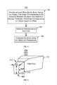
- FIG. 3depicts ABS, side, and top views of a conventional perpendicular magnetic recording (PMR) pole 40 that has a trailing edge bevel 42 .
- PMRperpendicular magnetic recording
- FIG. 3is not to scale.
- the conventional PMR pole 40also has sidewalls 44 having a reverse angle and flare point 46 .
- the conventional PMR pole 40has a top wider than its bottom. Because of the combination of the bevel 42 and sidewalls 44 , the windage, the track width, and the pole height change as part of the PMR pole 40 is lapped away.
- the geometry of the conventional PMR pole 40make lapping to the desired windage (nl), track width (tw), and pole height (H) challenging.
- processing variationsthat occur for the separate processes used in determining the flare point 46 , bevel 42 , and sidewalls 44 . Variations in these processes may cause variations in the shape or location of these features of the conventional PMR pole 40 . It would be desirable, therefore, to compensate for these processing variations.
- Use of the conventional ELG 10is not sufficient to do so.
- a method and system for calibrating an electronic lapping guide (ELG) for least one transducer having an air-bearing surface (ABS) and a magnetic structureis described.
- the magnetic structurehas a desired thickness, a bevel, and a flare point a distance from the ABS.
- the method and systeminclude providing at least three ELGs.
- the first ELGhas first and second edges first and second distances from the ABS. The first distance and/or the second distance correspond to an intersection between the bevel and the desired thickness.
- the second ELGhas a third edge a third distance from the ABS and a fourth edge the second distance from the ABS. The third distance and/or the second distance correspond to the intersection between the bevel and the desired thickness.
- the third ELGhas a fifth edge a fourth distance from the ABS and a sixth edge the second distance from the ABS.
- the first distance, the third distance, and the fourth distancecorrespond to a stripe height and an offset.
- the fourth distance and/or the second distancecorrespond to the intersection between the bevel and the desired thickness.
- the method and systemalso include measuring resistances of the first ELG, the second ELG, and the third ELG and calibrating the at least one ELG utilizing the offset and the resistances.
- FIG. 1depicts a conventional ELG as used in a conventional magnetic transducer.
- FIG. 2is a flow chart depicting a conventional method for performing lapping utilizing a conventional ELG.
- FIG. 3depicts a conventional PMR pole in a conventional PMR transducer.
- FIG. 4is a flow chart depicting an exemplary embodiment of a method for calibrating ELGs.
- FIG. 5depicts an exemplary embodiment of a transducer including a magnetic structure to be lapped using the ELGs.
- FIG. 6depicts another exemplary embodiment of a transducer including the ELGs.
- FIG. 7depicts another exemplary embodiment of a transducer including the ELGs.
- FIG. 8depicts another exemplary embodiment of a transducer including the ELGs.
- FIG. 9is a flow chart depicting an exemplary embodiment of a method for calibrating ELGs.
- FIGS. 10-11depict another exemplary embodiment of a transducer including the ELGs during fabrication of the ELGs.
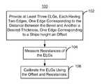
- FIG. 4is a flow chart depicting an exemplary embodiment of a method 100 for calibrating ELGs. For simplicity, some steps of the method 100 may be omitted.
- FIGS. 5-8depict exemplary embodiments of a portion of transducers 200 , 200 ′, and 200 ′′ with which the method 100 may be used. For clarity FIGS. 5-8 are not to scale.
- the transducers 200 , 200 ′, and 200 ′′each includes at least one magnetic structure 210 on which lapping is to be performed.
- the magnetic structure being fabricatedis shown in FIG. 5 .
- the transducer in FIG. 5is labeled 200 / 200 ′/ 200 ′′.
- the magnetic structure 210is a PMR pole having a desired thickness, h, a bevel 212 , and a flare point 216 a distance (NL) from the ABS.
- the PMR pole 210also includes sidewalls 214 having a reverse angle and is characterized by track width TW.
- the transducers 200 , 200 ′, and 200 ′′may be part of a merged head including a read transducer and the write transducer.
- the transducers 200 , 200 ′, and 200 ′′may thus be fabricated on wafer(s) which hold numerous transducers (not shown).
- the transducers 200 , 200 ′, and 200 ′′may be separated from the wafer(s) on which they were fabricated and incorporated into a hard disk drive.
- the transducers 200 , 200 ′, and 200 ′′may each reside on a slider (not shown).
- a magnetic structuremay include any structure formed in a magnetic transducer. In various embodiments, other numbers of ELGs per transducer and/or per magnetic structure, including greater or less than three per transducer/magnetic structure, may be used.
- the method 100 and transducers 200 , 200 ′, and 200 ′′are described in the context of a flare point 216 and bevel 212 .
- the flare pointcorresponds to a point of interest from which distance to the desired ABS/surface, such as a windage, is measured. Consequently, in some embodiments, the magnetic structure fabricated using the method 100 may include some other feature corresponding to the flare point.
- the bevelcorresponds to a surface, top or bottom, of the magnetic structure 210 which is not perpendicular to the ABS or which otherwise defines a location of interest on the magnetic structure.
- the method 100is also described in the context of single transducers 200 , 200 ′, and 200 ′′.
- the method 100may be used for fabricating multiple transducers and/or multiple structures and may employ multiple ELG(s) at substantially the same time.
- the magnetic structure 210 being fabricatedhas may be desired to adjoin the ABS.
- the lapping to be performed based on calibration using the method 100proceeds to the ABS location (the location at which the ABS is formed).
- the lappingmay be used to expose another surface.
- At least three ELGs having the desired offsets and stripe heightsare provided, via step 102 .
- Step 102may include depositing a resistive sheet and fabricating the three or more ELGs from the resistive sheet.
- the ELGsare configured so that one of their edges correspond to a particular position, such as the intersection between the bevel 212 and the desired thickness h. Such a position may correspond to the desired location of the ABS. However, another location such as the flare point may also be selected.
- the ELGsare also configured in step 102 such that another edge corresponds to the desired stripe height and an offset.
- the other edgesmay correspond to the stripe height, the stripe height plus an offset, and the stripe height minus an offset.
- the locations of the other edges of the three or more ELGsmay be expressed in terms of two variables (e.g. the stripe height and an offset).
- the ELGsmay be fabricated by using a single mask and shifting the reticle a known amount between the different ELGs. Shirting the reticle may provide the most reliable determination of the offsets. Portions of the ELGs may be removed to the same location, such as the intersection of bevel and the desired height. However, in another embodiment, another method for providing the offsets may be used.
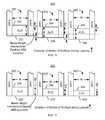
- FIG. 6depicts one embodiment of a transducer 200 after step 102 is performed.
- three ELGs 220 , 230 , and 240are shown.
- the ELGs 220 , 230 , and 240have edges 222 , 232 , and 242 , respectively, at a location defined by the intersection of the bevel and the desired height.
- the other edges 224 , 234 , and 244are located at the stripe height plus an offset (SH+ ⁇ ), the stripe height (SH) and the stripe height minus an offset (SH ⁇ ) from the bevel location.
- each of the ELGs 220 , 230 , and 240has a common location and lengths that differ in known ways.
- FIG. 7depicts another embodiment of a transducer 200 ′ after step 102 is performed.
- the ELGs 220 ′, 230 ′, and 240 ′have edges 224 ′, 234 ′, and 244 ′, respectively, at a known location.
- the edges 224 ′, 234 ′, and 244 ′may be at the flare point.
- the other edges 224 ′, 234 ′, and 244 ′are located at the stripe height plus an offset (SH+ ⁇ ), the stripe height (SH) and the stripe height minus an offset (SH ⁇ ) from the flare point.
- each of the ELGs 220 ′, 230 ′, and 240 ′has a common location and lengths that differ in known ways.
- FIG. 8depicts another embodiment of a transducer 200 ′′ after step 102 is performed.
- four ELGs 220 ′′, 230 ′′, 240 ′′, and 250are shown.
- the ELGs 220 ′′, 230 ′′, 240 ′′, and 250have edges 222 ′′, 232 ′′, 242 ′′, and 252 respectively, at a known location.
- the edges 222 ′′, 232 ′′, 242 ′′, and 252may be at the intersection between the bevel 212 and the desired height h (i.e. at the desired ABS).
- the other edges 224 ′′, 234 ′′, 244 ′′, and 254are located at the stripe height plus an offset (SH+ ⁇ ), the stripe height (SH) the stripe height minus an offset (SH ⁇ ), and the stripe height plus twice the offset (SH+2 ⁇ ) from the bevel 212 -height intersection.
- the offset, dmay vary.
- ⁇may be at least fifty nanometers and not more than one hundred nanometers.
- the offset ⁇may vary based on the structure 210 being fabricated and is generally desired to be in the process window range.
- each of the ELGs 220 ′′, 230 ′′, 240 ′′, and 250has a common location and lengths that differ in known ways.
- the resistances of the ELGsare measured, via step 104 .
- the resistances of the ELGs 220 , 230 , and 240are determined.
- the resistances of the ELGs 220 ′, 230 ′, and 240 ′are determined.
- the resistances of the ELGs 220 ′′, 230 ′′, 240 ′′, and 250are determined.
- Step 106may include determining the stripe height, a target resistance of each ELG, and a sheet resistance of the ELGs.
- the calibrationmay be determined using a linear model for the resistances.
- SH⁇ *(R 240 ⁇ R 220 )/(R 240 +R 220 ⁇ 2*R 230 ),
- R S *W2* ⁇ *(R 240 ⁇ R 220 )*(R 240 ⁇ R 230 )*(R 230 ⁇ R 220 )/[R 220 +R 240 ⁇ 2*R 230 ] 2 ;
- R L[2*R 220 *R 240 ⁇ R 240 *R 230 ⁇ R 230 *R 220 ]/(R 240 +R 220 ⁇ 2*R 230 ). Consequently, the stripe height and thus the windage can be determined. If more than three ELGs are used, then higher order terms or other variables might be taken into account. Thus, the stripe height and the resistance coefficient, or resistance per unit length, may be determined.
- the ELGs 220 , 230 , and 240 ; the ELGs 220 ′, 230 ′, and 240 ′, and the ELGs 220 ′′, 230 ′′, 240 ′′, and 250may be calibrated.
- the resistance per unit length of the ELGsmay be determined based on the resistances, stripe height, and offset.
- the stripe heights, SHcorrespond to the desired windage because the back edge 234 of the non-offset ELG 230 is desired to be aligned with the flare point 216 of the PMR pole 210 .
- the actual windagemay be calculated using the resistance per unit length and measured resistance of the ELGs during lapping.
- the actual windagemay be determined, variations in processing and other inconsistencies may be taken into account.
- the actual windage valuesmay be used in lapping the PMR pole 210 or other analogous structure. Consequently, better control of lapping and thus better control over the final structure may be achieved. Improvements in manufacturing and performance of the transducers 200 / 200 ′/ 200 ′′ may thus be accomplished.
- FIG. 9is a flow chart depicting another exemplary embodiment of a method 150 for calibrating ELGs. For simplicity, some steps of the method 150 may be omitted.
- FIGS. 10-11depict another exemplary embodiment of a transducer 300 including the ELGs 320 , 330 , and 340 during fabrication of the ELGs. For clarity, FIGS. 10-11 are not to scale.
- the transducer 300includes a magnetic structure such as the PMR pole 210 depicted in FIG. 5 and for fabrication of which the ELGs are desired to be calibrated.
- the magnetic structure 210is a PMR pole having a desired thickness, h, a bevel 212 , and a flare point 216 a distance (NL) from the ABS.
- the PMR pole 210also includes sidewalls 214 having a reverse angle and is characterized by a track width TW. Note that FIG. 5 depicts the PMR pole 210 after lapping to the ABS.
- the transducer 300is analogous to the transducer 200 .
- the transducer 300may thus be fabricated on wafer(s) which hold numerous transducers (not shown). Once fabrication is complete, or at some other point in processing, the transducers may be separated from the wafer(s) on which they were fabricated and incorporated into a hard disk drive.
- the transducer 300may reside on a slider (not shown).
- a magnetic structuremay include any structure formed in a magnetic transducer.
- ELGs per transducer and/or per magnetic structuremay be used.
- the method 100 and transducers 200 , 200 ′, and 200 ′′are described in the context of a flare point 216 and bevel 212 .
- the flare pointcorresponds to a point of interest from which distance to the desired ABS, such as a windage, is measured. Consequently, in some embodiments, the magnetic structure fabricated using the method 150 may include some other feature corresponding to the flare point.
- the bevelcorresponds to a surface, top or bottom, of the magnetic structure 210 which is not perpendicular to the ABS or which otherwise defines a location of interest on the magnetic structure.
- the method 150is also described in the context of single transducer 300 .
- the method 150may be used for fabricating multiple transducers and/or multiple structures and may employ multiple ELG(s) at substantially the same time.
- the magnetic structure 210 being fabricatedhas may be desired to adjoin the ABS.
- the lapping to be performed based on calibration using the method 150proceeds to the ABS location (the location at which the ABS is formed).
- the lappingmay be used to expose another surface.
- a resistive sheet substantially coplanar with the desired thickness, h, of the PMR poleis provided, via step 152 .
- the ELG'sare defined from the resistive sheet such that at least one of their edges are offset by known amounts, via step 154 .
- step 154is performed by shifting the reticle for each of the ELGs during mask formation, then using the mask formed by the shifted reticle to remove portions of the resistive sheet.
- FIG. 10depicts the transducer 300 after step 154 has been performed.
- ELGs 320 , 330 , and 340are shown.
- another number of ELGsmay be fabricated.
- Each ELGhas the same depth, d.
- the front edges 322 , 332 and 342 as well as the back edges 324 , 334 , and 344are offset due to the shift in the reticle.
- the reticlewould be at one location when the mask for the ELG 320 is formed, shifted by an amount corresponding to ⁇ when the mask for the ELG 330 is formed, and shifted again by an amount corresponding to ⁇ when the mask for the ELG 340 is formed.
- One set of the edgesis then set along a line, via step 156 .
- portions of the ELGs 320 , 330 , and 340 near the front edges 322 , 332 , and 342 , respectively,are removed.
- portions of the ELGs 320 , 330 , and 340 near the back edges 324 , 334 , and 344 , respectively,are removed.
- FIG. 11depicts the transducer 300 after step 158 is performed. In the embodiment shown, the front edges 322 ′, 332 ′, and 342 ′ have been set along the same line.
- thisis accomplished by exposing the ELGs 320 , 330 , and 340 in the same manner as the PMR pole 210 during formation of the bevel 212 .
- the same processing step, such as an ion mill, that forms the bevelalso forms the front edges 322 ′, 332 ′, and 342 ′.
- the front edges 322 ′, 332 ′, and 342 ′are at locations corresponding to the intersection of the bevel 212 and the desired height, h, of the PMR pole.
- the depth of the ELG 320 ′is now SH+ ⁇
- the depth of the ELG 330 ′is SH
- the depth of the ELG 340 ′is SH ⁇ .
- the offsets between the ELGs 320 ′, 330 ′, and 340 ′may differ as long the relationships between the offsets are known. Thus, using steps 154 and 156 , the ELGs 320 ′, 330 ′, and 340 ′ are formed.
- the resistances of the ELGs 320 ′, 330 ′, and 340 ′are measured, via step 158 .
- the ELGs 320 ′, 330 ′, and 340 ′are then calibrated using the offset, ⁇ , and the resistances measured, via step 160 .
- the linear model described abovemay be used in calibrating the ELGs 320 ′, 330 ′, and 340 ′.
- the stripe height, SH and offset dmay be calculated. Consequently, the windage (distance between the ABS and flare point 216 ) of the PMR pole 210 may be determined.
- the ELGs 320 ′, 330 ′, and 340 ′may be calibrated. More specifically, quantities such as the stripe height and resistance per unit length may be calculated. The lengths of the ELGs 320 ′, 330 ′, and 340 ′ during lapping may be determined based on the resistances. The final lengths of the ELGs 320 ′, 330 ′, and 340 ′ after lapping and thus the actual windage of the PMR pole 210 may also be determined. Because the actual windage may be determined, variations in processing and other inconsistencies may be taken into account. In particular, the actual windage values may be used in lapping the PMR pole 210 or other analogous structure. Consequently, better control of lapping and thus better control over the final structure may be achieved. Improvements in manufacturing and performance of the transducers 200 / 200 ′/ 200 ′′ may thus be accomplished.
Landscapes
- Engineering & Computer Science (AREA)
- Manufacturing & Machinery (AREA)
- Magnetic Heads (AREA)
Abstract
Description
Claims (11)
Priority Applications (2)
| Application Number | Priority Date | Filing Date | Title |
|---|---|---|---|
| US12/473,159US8291743B1 (en) | 2009-05-27 | 2009-05-27 | Method and system for calibrating an electronic lapping guide for a beveled pole in a magnetic recording transducer |
| US13/625,270US8717709B1 (en) | 2009-05-27 | 2012-09-24 | System for calibrating an electronic lapping guide for a beveled pole in a magnetic recording transducer |
Applications Claiming Priority (1)
| Application Number | Priority Date | Filing Date | Title |
|---|---|---|---|
| US12/473,159US8291743B1 (en) | 2009-05-27 | 2009-05-27 | Method and system for calibrating an electronic lapping guide for a beveled pole in a magnetic recording transducer |
Related Child Applications (1)
| Application Number | Title | Priority Date | Filing Date |
|---|---|---|---|
| US13/625,270DivisionUS8717709B1 (en) | 2009-05-27 | 2012-09-24 | System for calibrating an electronic lapping guide for a beveled pole in a magnetic recording transducer |
Publications (1)
| Publication Number | Publication Date |
|---|---|
| US8291743B1true US8291743B1 (en) | 2012-10-23 |
Family
ID=47017283
Family Applications (2)
| Application Number | Title | Priority Date | Filing Date |
|---|---|---|---|
| US12/473,159Expired - Fee RelatedUS8291743B1 (en) | 2009-05-27 | 2009-05-27 | Method and system for calibrating an electronic lapping guide for a beveled pole in a magnetic recording transducer |
| US13/625,270Active2029-06-22US8717709B1 (en) | 2009-05-27 | 2012-09-24 | System for calibrating an electronic lapping guide for a beveled pole in a magnetic recording transducer |
Family Applications After (1)
| Application Number | Title | Priority Date | Filing Date |
|---|---|---|---|
| US13/625,270Active2029-06-22US8717709B1 (en) | 2009-05-27 | 2012-09-24 | System for calibrating an electronic lapping guide for a beveled pole in a magnetic recording transducer |
Country Status (1)
| Country | Link |
|---|---|
| US (2) | US8291743B1 (en) |
Cited By (144)
| Publication number | Priority date | Publication date | Assignee | Title |
|---|---|---|---|---|
| US20120036706A1 (en)* | 2010-08-13 | 2012-02-16 | Sae Magnetics (H.K.) Ltd. | Row bar for forming sliders and method of manufacturing slider |
| US8443510B1 (en) | 2009-05-28 | 2013-05-21 | Western Digital (Fremont), Llc | Method for utilizing an electronic lapping guide for a beveled pole in a magnetic recording transducer |
| US8717709B1 (en) | 2009-05-27 | 2014-05-06 | Western Digital (Fremont), Llc | System for calibrating an electronic lapping guide for a beveled pole in a magnetic recording transducer |
| US8758083B1 (en)* | 2010-09-13 | 2014-06-24 | Western Digital (Fremont), Llc | Method and system for adjusting lapping of a transducer using a disk windage |
| US8830628B1 (en) | 2009-02-23 | 2014-09-09 | Western Digital (Fremont), Llc | Method and system for providing a perpendicular magnetic recording head |
| US8879207B1 (en) | 2011-12-20 | 2014-11-04 | Western Digital (Fremont), Llc | Method for providing a side shield for a magnetic recording transducer using an air bridge |
| US8883017B1 (en) | 2013-03-12 | 2014-11-11 | Western Digital (Fremont), Llc | Method and system for providing a read transducer having seamless interfaces |
| US8917581B1 (en) | 2013-12-18 | 2014-12-23 | Western Digital Technologies, Inc. | Self-anneal process for a near field transducer and chimney in a hard disk drive assembly |
| US8922954B2 (en) | 2013-05-06 | 2014-12-30 | Seagate Technology Llc | Data reader with back edge surface |
| US8923102B1 (en) | 2013-07-16 | 2014-12-30 | Western Digital (Fremont), Llc | Optical grating coupling for interferometric waveguides in heat assisted magnetic recording heads |
| US8947985B1 (en) | 2013-07-16 | 2015-02-03 | Western Digital (Fremont), Llc | Heat assisted magnetic recording transducers having a recessed pole |
| US8953422B1 (en) | 2014-06-10 | 2015-02-10 | Western Digital (Fremont), Llc | Near field transducer using dielectric waveguide core with fine ridge feature |
| US8958272B1 (en) | 2014-06-10 | 2015-02-17 | Western Digital (Fremont), Llc | Interfering near field transducer for energy assisted magnetic recording |
| US8970988B1 (en) | 2013-12-31 | 2015-03-03 | Western Digital (Fremont), Llc | Electric gaps and method for making electric gaps for multiple sensor arrays |
| US8971160B1 (en) | 2013-12-19 | 2015-03-03 | Western Digital (Fremont), Llc | Near field transducer with high refractive index pin for heat assisted magnetic recording |
| US8976635B1 (en) | 2014-06-10 | 2015-03-10 | Western Digital (Fremont), Llc | Near field transducer driven by a transverse electric waveguide for energy assisted magnetic recording |
| US8980109B1 (en) | 2012-12-11 | 2015-03-17 | Western Digital (Fremont), Llc | Method for providing a magnetic recording transducer using a combined main pole and side shield CMP for a wraparound shield scheme |
| US8982508B1 (en) | 2011-10-31 | 2015-03-17 | Western Digital (Fremont), Llc | Method for providing a side shield for a magnetic recording transducer |
| US8988825B1 (en) | 2014-02-28 | 2015-03-24 | Western Digital (Fremont, LLC | Method for fabricating a magnetic writer having half-side shields |
| US8988812B1 (en) | 2013-11-27 | 2015-03-24 | Western Digital (Fremont), Llc | Multi-sensor array configuration for a two-dimensional magnetic recording (TDMR) operation |
| US8984740B1 (en) | 2012-11-30 | 2015-03-24 | Western Digital (Fremont), Llc | Process for providing a magnetic recording transducer having a smooth magnetic seed layer |
| US8993217B1 (en) | 2013-04-04 | 2015-03-31 | Western Digital (Fremont), Llc | Double exposure technique for high resolution disk imaging |
| US8995087B1 (en) | 2006-11-29 | 2015-03-31 | Western Digital (Fremont), Llc | Perpendicular magnetic recording write head having a wrap around shield |
| US9001628B1 (en) | 2013-12-16 | 2015-04-07 | Western Digital (Fremont), Llc | Assistant waveguides for evaluating main waveguide coupling efficiency and diode laser alignment tolerances for hard disk |
| US8997832B1 (en) | 2010-11-23 | 2015-04-07 | Western Digital (Fremont), Llc | Method of fabricating micrometer scale components |
| US9001467B1 (en) | 2014-03-05 | 2015-04-07 | Western Digital (Fremont), Llc | Method for fabricating side shields in a magnetic writer |
| US9007719B1 (en) | 2013-10-23 | 2015-04-14 | Western Digital (Fremont), Llc | Systems and methods for using double mask techniques to achieve very small features |
| US9007879B1 (en) | 2014-06-10 | 2015-04-14 | Western Digital (Fremont), Llc | Interfering near field transducer having a wide metal bar feature for energy assisted magnetic recording |
| US9007725B1 (en) | 2014-10-07 | 2015-04-14 | Western Digital (Fremont), Llc | Sensor with positive coupling between dual ferromagnetic free layer laminates |
| US9013836B1 (en) | 2013-04-02 | 2015-04-21 | Western Digital (Fremont), Llc | Method and system for providing an antiferromagnetically coupled return pole |
| US9042208B1 (en) | 2013-03-11 | 2015-05-26 | Western Digital Technologies, Inc. | Disk drive measuring fly height by applying a bias voltage to an electrically insulated write component of a head |
| US9042057B1 (en) | 2013-01-09 | 2015-05-26 | Western Digital (Fremont), Llc | Methods for providing magnetic storage elements with high magneto-resistance using Heusler alloys |
| US9042051B2 (en) | 2013-08-15 | 2015-05-26 | Western Digital (Fremont), Llc | Gradient write gap for perpendicular magnetic recording writer |
| US9042058B1 (en) | 2013-10-17 | 2015-05-26 | Western Digital Technologies, Inc. | Shield designed for middle shields in a multiple sensor array |
| US9042052B1 (en) | 2014-06-23 | 2015-05-26 | Western Digital (Fremont), Llc | Magnetic writer having a partially shunted coil |
| US9053735B1 (en) | 2014-06-20 | 2015-06-09 | Western Digital (Fremont), Llc | Method for fabricating a magnetic writer using a full-film metal planarization |
| US9064527B1 (en) | 2013-04-12 | 2015-06-23 | Western Digital (Fremont), Llc | High order tapered waveguide for use in a heat assisted magnetic recording head |
| US9065043B1 (en) | 2012-06-29 | 2015-06-23 | Western Digital (Fremont), Llc | Tunnel magnetoresistance read head with narrow shield-to-shield spacing |
| US9064528B1 (en) | 2013-05-17 | 2015-06-23 | Western Digital Technologies, Inc. | Interferometric waveguide usable in shingled heat assisted magnetic recording in the absence of a near-field transducer |
| US9064507B1 (en) | 2009-07-31 | 2015-06-23 | Western Digital (Fremont), Llc | Magnetic etch-stop layer for magnetoresistive read heads |
| US9070381B1 (en) | 2013-04-12 | 2015-06-30 | Western Digital (Fremont), Llc | Magnetic recording read transducer having a laminated free layer |
| US9082423B1 (en) | 2013-12-18 | 2015-07-14 | Western Digital (Fremont), Llc | Magnetic recording write transducer having an improved trailing surface profile |
| US9087534B1 (en) | 2011-12-20 | 2015-07-21 | Western Digital (Fremont), Llc | Method and system for providing a read transducer having soft and hard magnetic bias structures |
| US9087527B1 (en) | 2014-10-28 | 2015-07-21 | Western Digital (Fremont), Llc | Apparatus and method for middle shield connection in magnetic recording transducers |
| US9093639B2 (en) | 2012-02-21 | 2015-07-28 | Western Digital (Fremont), Llc | Methods for manufacturing a magnetoresistive structure utilizing heating and cooling |
| US9104107B1 (en) | 2013-04-03 | 2015-08-11 | Western Digital (Fremont), Llc | DUV photoresist process |
| US9111564B1 (en) | 2013-04-02 | 2015-08-18 | Western Digital (Fremont), Llc | Magnetic recording writer having a main pole with multiple flare angles |
| US9111558B1 (en) | 2014-03-14 | 2015-08-18 | Western Digital (Fremont), Llc | System and method of diffractive focusing of light in a waveguide |
| US9111550B1 (en) | 2014-12-04 | 2015-08-18 | Western Digital (Fremont), Llc | Write transducer having a magnetic buffer layer spaced between a side shield and a write pole by non-magnetic layers |
| US9123362B1 (en) | 2011-03-22 | 2015-09-01 | Western Digital (Fremont), Llc | Methods for assembling an electrically assisted magnetic recording (EAMR) head |
| US9123359B1 (en) | 2010-12-22 | 2015-09-01 | Western Digital (Fremont), Llc | Magnetic recording transducer with sputtered antiferromagnetic coupling trilayer between plated ferromagnetic shields and method of fabrication |
| US9123374B1 (en) | 2015-02-12 | 2015-09-01 | Western Digital (Fremont), Llc | Heat assisted magnetic recording writer having an integrated polarization rotation plate |
| US9123358B1 (en) | 2012-06-11 | 2015-09-01 | Western Digital (Fremont), Llc | Conformal high moment side shield seed layer for perpendicular magnetic recording writer |
| US9129660B2 (en) | 2013-12-04 | 2015-09-08 | HGST Netherlands B.V. | Transducer resistor shunt structure for low-cost probing |
| US9135937B1 (en) | 2014-05-09 | 2015-09-15 | Western Digital (Fremont), Llc | Current modulation on laser diode for energy assisted magnetic recording transducer |
| US9135930B1 (en) | 2014-03-06 | 2015-09-15 | Western Digital (Fremont), Llc | Method for fabricating a magnetic write pole using vacuum deposition |
| US9142233B1 (en) | 2014-02-28 | 2015-09-22 | Western Digital (Fremont), Llc | Heat assisted magnetic recording writer having a recessed pole |
| US9147404B1 (en) | 2015-03-31 | 2015-09-29 | Western Digital (Fremont), Llc | Method and system for providing a read transducer having a dual free layer |
| US9147408B1 (en) | 2013-12-19 | 2015-09-29 | Western Digital (Fremont), Llc | Heated AFM layer deposition and cooling process for TMR magnetic recording sensor with high pinning field |
| US9153260B1 (en) | 2008-03-27 | 2015-10-06 | Western Digital (Fremont), Llc | Electronic lapping guide in a magnetic recording transducer |
| US9153255B1 (en) | 2014-03-05 | 2015-10-06 | Western Digital (Fremont), Llc | Method for fabricating a magnetic writer having an asymmetric gap and shields |
| US9183854B2 (en) | 2014-02-24 | 2015-11-10 | Western Digital (Fremont), Llc | Method to make interferometric taper waveguide for HAMR light delivery |
| US9190085B1 (en) | 2014-03-12 | 2015-11-17 | Western Digital (Fremont), Llc | Waveguide with reflective grating for localized energy intensity |
| US9190079B1 (en) | 2014-09-22 | 2015-11-17 | Western Digital (Fremont), Llc | Magnetic write pole having engineered radius of curvature and chisel angle profiles |
| US9194692B1 (en) | 2013-12-06 | 2015-11-24 | Western Digital (Fremont), Llc | Systems and methods for using white light interferometry to measure undercut of a bi-layer structure |
| US9202480B2 (en) | 2009-10-14 | 2015-12-01 | Western Digital (Fremont), LLC. | Double patterning hard mask for damascene perpendicular magnetic recording (PMR) writer |
| US9202493B1 (en) | 2014-02-28 | 2015-12-01 | Western Digital (Fremont), Llc | Method of making an ultra-sharp tip mode converter for a HAMR head |
| US9214169B1 (en) | 2014-06-20 | 2015-12-15 | Western Digital (Fremont), Llc | Magnetic recording read transducer having a laminated free layer |
| US9214172B2 (en) | 2013-10-23 | 2015-12-15 | Western Digital (Fremont), Llc | Method of manufacturing a magnetic read head |
| US9214165B1 (en) | 2014-12-18 | 2015-12-15 | Western Digital (Fremont), Llc | Magnetic writer having a gradient in saturation magnetization of the shields |
| US9213322B1 (en) | 2012-08-16 | 2015-12-15 | Western Digital (Fremont), Llc | Methods for providing run to run process control using a dynamic tuner |
| US9230565B1 (en) | 2014-06-24 | 2016-01-05 | Western Digital (Fremont), Llc | Magnetic shield for magnetic recording head |
| US9236560B1 (en) | 2014-12-08 | 2016-01-12 | Western Digital (Fremont), Llc | Spin transfer torque tunneling magnetoresistive device having a laminated free layer with perpendicular magnetic anisotropy |
| US9245543B1 (en) | 2010-06-25 | 2016-01-26 | Western Digital (Fremont), Llc | Method for providing an energy assisted magnetic recording head having a laser integrally mounted to the slider |
| US9245562B1 (en) | 2015-03-30 | 2016-01-26 | Western Digital (Fremont), Llc | Magnetic recording writer with a composite main pole |
| US9245545B1 (en) | 2013-04-12 | 2016-01-26 | Wester Digital (Fremont), Llc | Short yoke length coils for magnetic heads in disk drives |
| US9251813B1 (en) | 2009-04-19 | 2016-02-02 | Western Digital (Fremont), Llc | Method of making a magnetic recording head |
| US9263071B1 (en) | 2015-03-31 | 2016-02-16 | Western Digital (Fremont), Llc | Flat NFT for heat assisted magnetic recording |
| US9263067B1 (en) | 2013-05-29 | 2016-02-16 | Western Digital (Fremont), Llc | Process for making PMR writer with constant side wall angle |
| US9269382B1 (en) | 2012-06-29 | 2016-02-23 | Western Digital (Fremont), Llc | Method and system for providing a read transducer having improved pinning of the pinned layer at higher recording densities |
| US9275657B1 (en) | 2013-08-14 | 2016-03-01 | Western Digital (Fremont), Llc | Process for making PMR writer with non-conformal side gaps |
| US9280990B1 (en) | 2013-12-11 | 2016-03-08 | Western Digital (Fremont), Llc | Method for fabricating a magnetic writer using multiple etches |
| US20160071535A1 (en)* | 2013-10-14 | 2016-03-10 | Seagate Technology Llc | Methods of manufacturing magnetic heads using a trigger reader electronic lapping guide |
| US9286919B1 (en) | 2014-12-17 | 2016-03-15 | Western Digital (Fremont), Llc | Magnetic writer having a dual side gap |
| US9287494B1 (en) | 2013-06-28 | 2016-03-15 | Western Digital (Fremont), Llc | Magnetic tunnel junction (MTJ) with a magnesium oxide tunnel barrier |
| US9305583B1 (en) | 2014-02-18 | 2016-04-05 | Western Digital (Fremont), Llc | Method for fabricating a magnetic writer using multiple etches of damascene materials |
| US9312064B1 (en) | 2015-03-02 | 2016-04-12 | Western Digital (Fremont), Llc | Method to fabricate a magnetic head including ion milling of read gap using dual layer hard mask |
| US9318130B1 (en) | 2013-07-02 | 2016-04-19 | Western Digital (Fremont), Llc | Method to fabricate tunneling magnetic recording heads with extended pinned layer |
| US9336814B1 (en) | 2013-03-12 | 2016-05-10 | Western Digital (Fremont), Llc | Inverse tapered waveguide for use in a heat assisted magnetic recording head |
| US9343087B1 (en) | 2014-12-21 | 2016-05-17 | Western Digital (Fremont), Llc | Method for fabricating a magnetic writer having half shields |
| US9343086B1 (en) | 2013-09-11 | 2016-05-17 | Western Digital (Fremont), Llc | Magnetic recording write transducer having an improved sidewall angle profile |
| US9343098B1 (en) | 2013-08-23 | 2016-05-17 | Western Digital (Fremont), Llc | Method for providing a heat assisted magnetic recording transducer having protective pads |
| US9349394B1 (en) | 2013-10-18 | 2016-05-24 | Western Digital (Fremont), Llc | Method for fabricating a magnetic writer having a gradient side gap |
| US9349392B1 (en) | 2012-05-24 | 2016-05-24 | Western Digital (Fremont), Llc | Methods for improving adhesion on dielectric substrates |
| US9361914B1 (en) | 2014-06-18 | 2016-06-07 | Western Digital (Fremont), Llc | Magnetic sensor with thin capping layer |
| US9361913B1 (en) | 2013-06-03 | 2016-06-07 | Western Digital (Fremont), Llc | Recording read heads with a multi-layer AFM layer methods and apparatuses |
| US9368134B1 (en) | 2010-12-16 | 2016-06-14 | Western Digital (Fremont), Llc | Method and system for providing an antiferromagnetically coupled writer |
| US9384763B1 (en) | 2015-03-26 | 2016-07-05 | Western Digital (Fremont), Llc | Dual free layer magnetic reader having a rear bias structure including a soft bias layer |
| US9384765B1 (en) | 2015-09-24 | 2016-07-05 | Western Digital (Fremont), Llc | Method and system for providing a HAMR writer having improved optical efficiency |
| US9387568B1 (en) | 2013-02-27 | 2016-07-12 | Western Digital Technologies, Inc. | Systems and methods for correcting fabrication error in magnetic recording heads using magnetic write width measurements |
| US9396743B1 (en) | 2014-02-28 | 2016-07-19 | Western Digital (Fremont), Llc | Systems and methods for controlling soft bias thickness for tunnel magnetoresistance readers |
| US9396742B1 (en) | 2012-11-30 | 2016-07-19 | Western Digital (Fremont), Llc | Magnetoresistive sensor for a magnetic storage system read head, and fabrication method thereof |
| US9406331B1 (en) | 2013-06-17 | 2016-08-02 | Western Digital (Fremont), Llc | Method for making ultra-narrow read sensor and read transducer device resulting therefrom |
| US9424866B1 (en) | 2015-09-24 | 2016-08-23 | Western Digital (Fremont), Llc | Heat assisted magnetic recording write apparatus having a dielectric gap |
| US9431039B1 (en) | 2013-05-21 | 2016-08-30 | Western Digital (Fremont), Llc | Multiple sensor array usable in two-dimensional magnetic recording |
| US9431031B1 (en) | 2015-03-24 | 2016-08-30 | Western Digital (Fremont), Llc | System and method for magnetic transducers having multiple sensors and AFC shields |
| US9431038B1 (en) | 2015-06-29 | 2016-08-30 | Western Digital (Fremont), Llc | Method for fabricating a magnetic write pole having an improved sidewall angle profile |
| US9431047B1 (en) | 2013-05-01 | 2016-08-30 | Western Digital (Fremont), Llc | Method for providing an improved AFM reader shield |
| US9431032B1 (en) | 2013-08-14 | 2016-08-30 | Western Digital (Fremont), Llc | Electrical connection arrangement for a multiple sensor array usable in two-dimensional magnetic recording |
| US9437251B1 (en) | 2014-12-22 | 2016-09-06 | Western Digital (Fremont), Llc | Apparatus and method having TDMR reader to reader shunts |
| US9443541B1 (en) | 2015-03-24 | 2016-09-13 | Western Digital (Fremont), Llc | Magnetic writer having a gradient in saturation magnetization of the shields and return pole |
| US9441938B1 (en) | 2013-10-08 | 2016-09-13 | Western Digital (Fremont), Llc | Test structures for measuring near field transducer disc length |
| US9449625B1 (en) | 2014-12-24 | 2016-09-20 | Western Digital (Fremont), Llc | Heat assisted magnetic recording head having a plurality of diffusion barrier layers |
| US9449621B1 (en) | 2015-03-26 | 2016-09-20 | Western Digital (Fremont), Llc | Dual free layer magnetic reader having a rear bias structure having a high aspect ratio |
| US9472216B1 (en) | 2015-09-23 | 2016-10-18 | Western Digital (Fremont), Llc | Differential dual free layer magnetic reader |
| US9484051B1 (en) | 2015-11-09 | 2016-11-01 | The Provost, Fellows, Foundation Scholars and the other members of Board, of the College of the Holy and Undivided Trinity of Queen Elizabeth near Dublin | Method and system for reducing undesirable reflections in a HAMR write apparatus |
| US9508363B1 (en) | 2014-06-17 | 2016-11-29 | Western Digital (Fremont), Llc | Method for fabricating a magnetic write pole having a leading edge bevel |
| US9508372B1 (en) | 2015-06-03 | 2016-11-29 | Western Digital (Fremont), Llc | Shingle magnetic writer having a low sidewall angle pole |
| US9508365B1 (en) | 2015-06-24 | 2016-11-29 | Western Digital (Fremont), LLC. | Magnetic reader having a crystal decoupling structure |
| US9530443B1 (en) | 2015-06-25 | 2016-12-27 | Western Digital (Fremont), Llc | Method for fabricating a magnetic recording device having a high aspect ratio structure |
| US9564150B1 (en) | 2015-11-24 | 2017-02-07 | Western Digital (Fremont), Llc | Magnetic read apparatus having an improved read sensor isolation circuit |
| US9595273B1 (en) | 2015-09-30 | 2017-03-14 | Western Digital (Fremont), Llc | Shingle magnetic writer having nonconformal shields |
| US9646639B2 (en) | 2015-06-26 | 2017-05-09 | Western Digital (Fremont), Llc | Heat assisted magnetic recording writer having integrated polarization rotation waveguides |
| US9666214B1 (en) | 2015-09-23 | 2017-05-30 | Western Digital (Fremont), Llc | Free layer magnetic reader that may have a reduced shield-to-shield spacing |
| US9721595B1 (en) | 2014-12-04 | 2017-08-01 | Western Digital (Fremont), Llc | Method for providing a storage device |
| US9740805B1 (en) | 2015-12-01 | 2017-08-22 | Western Digital (Fremont), Llc | Method and system for detecting hotspots for photolithographically-defined devices |
| US9741366B1 (en) | 2014-12-18 | 2017-08-22 | Western Digital (Fremont), Llc | Method for fabricating a magnetic writer having a gradient in saturation magnetization of the shields |
| US9754611B1 (en) | 2015-11-30 | 2017-09-05 | Western Digital (Fremont), Llc | Magnetic recording write apparatus having a stepped conformal trailing shield |
| US9767831B1 (en) | 2015-12-01 | 2017-09-19 | Western Digital (Fremont), Llc | Magnetic writer having convex trailing surface pole and conformal write gap |
| US9786301B1 (en) | 2014-12-02 | 2017-10-10 | Western Digital (Fremont), Llc | Apparatuses and methods for providing thin shields in a multiple sensor array |
| US9799351B1 (en) | 2015-11-30 | 2017-10-24 | Western Digital (Fremont), Llc | Short yoke length writer having assist coils |
| US9812155B1 (en) | 2015-11-23 | 2017-11-07 | Western Digital (Fremont), Llc | Method and system for fabricating high junction angle read sensors |
| US9842615B1 (en) | 2015-06-26 | 2017-12-12 | Western Digital (Fremont), Llc | Magnetic reader having a nonmagnetic insertion layer for the pinning layer |
| US9858951B1 (en) | 2015-12-01 | 2018-01-02 | Western Digital (Fremont), Llc | Method for providing a multilayer AFM layer in a read sensor |
| US9881638B1 (en) | 2014-12-17 | 2018-01-30 | Western Digital (Fremont), Llc | Method for providing a near-field transducer (NFT) for a heat assisted magnetic recording (HAMR) device |
| US9934811B1 (en) | 2014-03-07 | 2018-04-03 | Western Digital (Fremont), Llc | Methods for controlling stray fields of magnetic features using magneto-elastic anisotropy |
| US9953670B1 (en) | 2015-11-10 | 2018-04-24 | Western Digital (Fremont), Llc | Method and system for providing a HAMR writer including a multi-mode interference device |
| US10037770B1 (en) | 2015-11-12 | 2018-07-31 | Western Digital (Fremont), Llc | Method for providing a magnetic recording write apparatus having a seamless pole |
| US10074387B1 (en) | 2014-12-21 | 2018-09-11 | Western Digital (Fremont), Llc | Method and system for providing a read transducer having symmetric antiferromagnetically coupled shields |
| US10354681B1 (en) | 2018-06-28 | 2019-07-16 | Sandisk Technologies Llc | Tunnel magnetoresistance read head including side shields containing nanocrystalline ferromagnetic particles |
| US10629230B2 (en) | 2017-04-20 | 2020-04-21 | Western Digital Technologies, Inc. | Method of forming a magnetic head |
| US10755733B1 (en) | 2019-03-05 | 2020-08-25 | Sandisk Technologies Llc | Read head including semiconductor spacer and long spin diffusion length nonmagnetic conductive material and method of making thereof |
| US11626137B1 (en) | 2022-01-31 | 2023-04-11 | Western Digital Technologies, Inc. | Heat assisted magnetic recording (HAMR) write head containing a near-field transducer with diffusion barrier and method of making thereof |
| US12411403B2 (en) | 2022-07-22 | 2025-09-09 | Western Digital Technologies, Inc. | Method of making a hard disk drive write pole using a tri-tone attenuated phase shift mask |
Citations (79)
| Publication number | Priority date | Publication date | Assignee | Title |
|---|---|---|---|---|
| US4157497A (en) | 1978-01-05 | 1979-06-05 | Rockwell International Corporation | Qualification test of gallium arsenide |
| US4670732A (en) | 1985-08-15 | 1987-06-02 | International Business Machines | Electrical lapping guide resistor |
| US4675986A (en) | 1985-07-29 | 1987-06-30 | International Business Machines | Electrical lapping guide for controlling the batch fabrication of thin film magnetic transducers |
| US5065483A (en) | 1991-02-19 | 1991-11-19 | International Business Machines Corporation | Method of lapping magnetic recording heads |
| US5210667A (en) | 1991-02-19 | 1993-05-11 | International Business Machines Corporation | Magnetic recording heads employing multiple lapping guides |
| US5361547A (en) | 1992-08-28 | 1994-11-08 | International Business Machines Corporation | Ultimate inductive head integrated lapping system |
| US5678086A (en) | 1996-07-22 | 1997-10-14 | Eastman Kodak Company | Patterned multi-track thin film heads for image area record/reproduce on magnetics-on-film |
| US5722155A (en) | 1996-01-11 | 1998-03-03 | Seagate Technology, Inc. | Machining guide method for magnetic recording reproduce heads |
| US5742995A (en) | 1996-05-24 | 1998-04-28 | Seagate Technology, Inc. | Method to predict an accurate MR sensor dimension when viewed from abs |
| US5772493A (en) | 1995-07-31 | 1998-06-30 | Read-Rite Corporation | Method and apparatus for controlling the lapping of magnetic heads |
| US5876264A (en) | 1997-04-25 | 1999-03-02 | International Business Machines Corporation | Deposition process windage calibration |
| US6027397A (en) | 1997-04-25 | 2000-02-22 | International Business Machines Corporation | Dual element lapping guide system |
| JP2000067408A (en) | 1998-08-25 | 2000-03-03 | Fujitsu Ltd | Manufacturing method of magnetic head |
| US6047224A (en) | 1996-04-10 | 2000-04-04 | Seagate Techology, Inc. | Machining guide for magnetic recording reproduce heads |
| US6083081A (en) | 1997-08-07 | 2000-07-04 | Tdk Corporation | Lapping control sensor for magnetoresistive effect head, lapping control method using the sensor and manufacturing method of the sensor |
| US6193584B1 (en) | 1999-05-27 | 2001-02-27 | Read-Rite Corporation | Apparatus and method of device stripe height control |
| US20010004800A1 (en) | 1997-10-28 | 2001-06-28 | Tdk Corporation | Method for manufacturing thin-film magnetic head and manufacturing system of the head |
| US6288870B1 (en) | 1998-01-13 | 2001-09-11 | Quantum Corporation | Self-aligned metal film core multi-channel recording head for tape drives |
| US20010051491A1 (en) | 1996-12-13 | 2001-12-13 | Shanlin Hao | Multipoint bending apparatus for lapping heads of a data storage device |
| US20020012204A1 (en) | 2000-05-25 | 2002-01-31 | Zine-Eddine Boutaghou | Lapping sensor for recording heads |
| US6347983B1 (en) | 1999-06-09 | 2002-02-19 | Seagate Technology Llc | ELG for both MRE sensor height and resistance monitoring |
| US6364743B1 (en) | 1999-06-11 | 2002-04-02 | Seagate Technology Llc | Composite lapping monitor resistor |
| US6399401B1 (en) | 2001-07-24 | 2002-06-04 | Advanced Micro Devices, In. | Test structures for electrical linewidth measurement and processes for their formation |
| US20020173227A1 (en) | 2001-03-16 | 2002-11-21 | Lam Chuck Fai | Embedded lapping guide |
| US20030020467A1 (en) | 2001-07-30 | 2003-01-30 | Tdk Corporation | Lapping monitor element, combined magnetic transducer element and lapping monitor element, and method for manufacturing magnetic transducer element |
| US20030021069A1 (en) | 2001-07-30 | 2003-01-30 | Crawforth Linden James | Slider having integrated lapping guides |
| US6609948B1 (en) | 2000-11-27 | 2003-08-26 | International Business Machines Corporation | Method of making an electronic lapping guide (ELG) for lapping a read sensor |
| US6623330B2 (en) | 2001-02-08 | 2003-09-23 | Sae Magnetics (H. K.) Ltd. | Lapping sensor used in fabrication of magnetic head with magnetoresistive effect element and lapping control method using the sensor |
| US6674610B1 (en) | 2000-06-16 | 2004-01-06 | Western Digital (Fremont), Inc. | Thin film write head with universal coil design |
| US20040009739A1 (en) | 2002-07-12 | 2004-01-15 | Li-Yan Zhu | Dual-purpose lapping guide for the production of magneto-resistive heads |
| US6684171B2 (en) | 2002-04-22 | 2004-01-27 | International Business Machines Corporation | In-situ stripe height calibration of magneto resistive sensors |
| US6699102B2 (en) | 2001-01-12 | 2004-03-02 | International Business Machines Corporation | Lapping monitor for monitoring the lapping of transducers |
| US20040075942A1 (en) | 2002-05-30 | 2004-04-22 | Bajorek Christopher H. | Lapping a head while powered up to eliminate expansion of the head due to heating |
| US20040097173A1 (en) | 2002-11-19 | 2004-05-20 | International Business Machines Corporation | Onboard multiphase electronic lapping guide design for MR heads |
| US6793557B2 (en) | 2002-05-24 | 2004-09-21 | International Business Machines Corporation | Removable lapping guide for magnetic recording head and method of use |
| US6846222B2 (en) | 2003-03-04 | 2005-01-25 | Hitachi Global Storage Technologies Netherlands, B.V. | Multi-chambered, compliant apparatus for restraining workpiece and applying variable pressure thereto during lapping to improve flatness characteristics of workpiece |
| US20050023673A1 (en) | 2003-07-25 | 2005-02-03 | Stefan Nowak | Transistor module |
| US20050028354A1 (en) | 2000-06-16 | 2005-02-10 | Tdk Corporation | Device and method for measuring amount of grinding in magnetic head producing process |
| US20050070206A1 (en) | 2003-09-29 | 2005-03-31 | Prakash Kasiraj | Slider fabrication system for sliders with integrated electrical lapping guides |
| US6884148B1 (en) | 2004-05-26 | 2005-04-26 | Headway Technologies, Inc. | Independently controlled read and write head stripe height parameters in slider back end process |
| US20050180048A1 (en) | 2004-02-13 | 2005-08-18 | Hitachi Global Technologies Netherlands B.V. | Perpendicular magnetic recording head built using an air-bearing surface damascene process |
| US20050185345A1 (en) | 2004-02-20 | 2005-08-25 | Meng Ding | Electrical lapping guide embedded in a shield of a magnetic head |
| US6935923B2 (en) | 2003-03-12 | 2005-08-30 | Seagate Technology Llc | Sensor stripe encapsulation layer in a read/write head |
| US20050219752A1 (en) | 2004-04-05 | 2005-10-06 | Alps Electric Co., Ltd. | Vertical recording magnetic head and method of manufacturing the same |
| US6982042B2 (en) | 2003-02-28 | 2006-01-03 | Hitachi Global Storage Technologies Netherlands, B.V. | Ion bombardment of electrical lapping guides to decrease noise during lapping process |
| US20060028770A1 (en) | 2004-08-03 | 2006-02-09 | Hitachi Global Storage Technologies Netherlands B.V. | Magnetic head with electro lapping guide and manufacturing method |
| US20060034021A1 (en) | 2004-08-13 | 2006-02-16 | Wu Andrew L | Methods of manufacturing magnetic heads with reference and monitoring devices |
| US20060044683A1 (en) | 2004-09-01 | 2006-03-02 | Sae Magnetics (H.K.) Ltd. | Thin film magnetic head structure, method of manufacturing the same, and method of manufacturing thin film magnetic head |
| US20060103990A1 (en) | 2004-11-16 | 2006-05-18 | Sae Magnetics (H.K.) Ltd. | Magnetic head manufacturing method, magnetic head, angle setting device and lapping device |
| US20060126222A1 (en) | 2004-10-20 | 2006-06-15 | Tdk Corporation | Thin film magnetic head, method of manufacturing the same, and magnetic recording apparatus |
| US20060139802A1 (en) | 2004-12-28 | 2006-06-29 | Headway Technologies, Inc. | Method of manufacturing magnetic head, and magnetic head sub-structure |
| US20060168798A1 (en) | 2005-01-31 | 2006-08-03 | Kabushiki Kaisha Toshiba | Method of lapping row bar in which perpendicular magnetic heads are formed and lapping machine |
| US7139152B2 (en) | 2003-10-20 | 2006-11-21 | Quantum Corporation | Servo methods and systems using existing data structures and optical masks |
| US7149061B2 (en) | 2001-07-31 | 2006-12-12 | Hitachi, Ltd. | Magnetic head with electro-lapping guide |
| US20070070543A1 (en) | 2005-09-29 | 2007-03-29 | Hitachi Global Storage Technologies Netherlands B.V. | Lapping method and station to achieve tight dimension controls for both read and write elements of magnetic recording heads and magnetic storage device formed thereby |
| US7244169B2 (en) | 2004-09-30 | 2007-07-17 | Hitachi Global Storage Technologies Netherlands Bv | In-line contiguous resistive lapping guide for magnetic sensors |
| US7245459B2 (en) | 2004-09-30 | 2007-07-17 | Hitachi Global Storage Technologies Netherlands Bv | Critically exposed lapping of magnetic sensors for target signal output |
| US7272883B2 (en) | 2003-08-29 | 2007-09-25 | Hitachi Global Storage Technologies Netherlands B.V. | Methods of forming an electrical connection in a magnetic head using a damascene process |
| US20070246761A1 (en) | 2006-04-19 | 2007-10-25 | Beach Robert S | Electrical lapping guides made from tunneling magnetoresistive (tmr) material |
| US20080072418A1 (en) | 2006-09-01 | 2008-03-27 | Hitachi Global Storage Technologies Netherlands B.V. | Method for manufacturing a magnetic head slider |
| US7360296B2 (en) | 2004-09-30 | 2008-04-22 | Hitachi Global Storage Technologies Netherlands B.V. | Method for reducing damage to sliders during lapping |
| US20080144215A1 (en) | 2006-12-15 | 2008-06-19 | Hitachi Global Storage Technologies | Electrical lapping guide for flare point control and trailing shield throat height in a perpendicular magnetic write head |
| US7393262B2 (en) | 2001-08-23 | 2008-07-01 | International Business Machines Corporation | Apparatus including pin adapter for air bearing surface (ABS) lapping |
| US7422511B2 (en) | 2006-06-12 | 2008-09-09 | Sae Magnetics (H.K.) Ltd. | Element for detecting the amount of lapping having a resistive film electrically connected to the substrate |
| US20080273275A1 (en) | 2007-05-04 | 2008-11-06 | Jeffrey S Lille | Fabricating a write head with multiple electronic lapping guides |
| US20090152235A1 (en) | 2007-12-13 | 2009-06-18 | Wen-Chien David Hsiao | Method of manufacturing a perpendicular magnetic write head with stepped trailing magnetic shield with electrical lapping guide control |
| US7551406B1 (en) | 2005-07-01 | 2009-06-23 | Western Digital (Fremont), Llc | Dual electrical lapping guides with common bonding pad |
| US7554767B1 (en) | 2005-07-01 | 2009-06-30 | Western Digital (Fremont), Llc | Electrical lapping guide disposed laterally relative to a shield pedestal |
| US20090211081A1 (en) | 2008-02-25 | 2009-08-27 | Boone Jr Thomas D | Controlled lapping for an abs damascene process |
| US7603762B2 (en) | 2006-12-15 | 2009-10-20 | Hitachi Global Storage Technologies Netherlands B.V. | Optical lapping guide for use in the manufacture of perpendicular magnetic write heads |
| US20090268348A1 (en) | 2008-04-28 | 2009-10-29 | Christian Rene Bonhote | Write head lapping guide about aligned to a non-magnetic layer surrounding a write pole and a method for making the same |
| US7643250B2 (en) | 2006-01-27 | 2010-01-05 | Hitachi Global Storage Technologies Netherlands B.V. | Pad slider design for on-slider ELGs |
| US7716814B2 (en) | 2007-02-05 | 2010-05-18 | Headway Technologies, Inc. | Method of manufacturing magnetic head, and magnetic head substructure |
| US20100162556A1 (en) | 2008-12-30 | 2010-07-01 | Unal Murat Guruz | Electrical lapping guide for improving magnetic core width in a magnetic recording head |
| US20100165513A1 (en) | 2008-12-31 | 2010-07-01 | Christian Rene Bonhote | Write head with self-align layer and a method for making the same |
| US7770281B2 (en) | 2007-05-10 | 2010-08-10 | Hitachi Global Storage Technologies Netherlands B.V. | Method for redefining the trailing shield throat height in a perpendicular magnetic recording write head |
| US20100208391A1 (en) | 2009-02-13 | 2010-08-19 | Seagate Technology Llc | Lapping Guides For Magnetic Recording Heads |
| US8151441B1 (en) | 2008-03-27 | 2012-04-10 | Western Digital (Fremont), Llc | Method for providing and utilizing an electronic lapping guide in a magnetic recording transducer |
| US8165709B1 (en) | 2009-02-26 | 2012-04-24 | Western Digital (Fremont), Llc | Four pad self-calibrating electronic lapping guide |
Family Cites Families (8)
| Publication number | Priority date | Publication date | Assignee | Title |
|---|---|---|---|---|
| US5805391A (en) | 1996-10-28 | 1998-09-08 | International Business Machines Corporation | Write head with recessed stitched yoke on a planar portion of an insulation layer defining zero throat height |
| US5963784A (en) | 1997-05-09 | 1999-10-05 | Vlsi Technology, Inc. | Methods of determining parameters of a semiconductor device and the width of an insulative spacer of a semiconductor device |
| US6131271A (en) | 1999-06-25 | 2000-10-17 | International Business Machines Corporation | Method of planarizing first pole piece layer of write head by lapping without delamination of first pole piece layer from wafer substrate |
| US7196871B2 (en)* | 2003-09-26 | 2007-03-27 | Hitachi Global Storage Technologies Netherlands B.V. | Head for perpendicular recording with a floating trailing shield |
| US8291743B1 (en) | 2009-05-27 | 2012-10-23 | Western Digital (Fremont), Llc | Method and system for calibrating an electronic lapping guide for a beveled pole in a magnetic recording transducer |
| US8443510B1 (en) | 2009-05-28 | 2013-05-21 | Western Digital (Fremont), Llc | Method for utilizing an electronic lapping guide for a beveled pole in a magnetic recording transducer |
| US8307539B1 (en) | 2009-09-30 | 2012-11-13 | Western Digital (Fremont), Llc | Method for modeling devices in a wafer |
| US8587899B1 (en)* | 2012-08-24 | 2013-11-19 | Headway Technologies, Inc. | Magnetic head for perpendicular magnetic recording having a bottom shield including a base part and a protruding part |
- 2009
- 2009-05-27USUS12/473,159patent/US8291743B1/ennot_activeExpired - Fee Related
- 2012
- 2012-09-24USUS13/625,270patent/US8717709B1/enactiveActive
Patent Citations (104)
| Publication number | Priority date | Publication date | Assignee | Title |
|---|---|---|---|---|
| US4157497A (en) | 1978-01-05 | 1979-06-05 | Rockwell International Corporation | Qualification test of gallium arsenide |
| US4675986A (en) | 1985-07-29 | 1987-06-30 | International Business Machines | Electrical lapping guide for controlling the batch fabrication of thin film magnetic transducers |
| US4670732A (en) | 1985-08-15 | 1987-06-02 | International Business Machines | Electrical lapping guide resistor |
| US5065483A (en) | 1991-02-19 | 1991-11-19 | International Business Machines Corporation | Method of lapping magnetic recording heads |
| US5210667A (en) | 1991-02-19 | 1993-05-11 | International Business Machines Corporation | Magnetic recording heads employing multiple lapping guides |
| US5361547A (en) | 1992-08-28 | 1994-11-08 | International Business Machines Corporation | Ultimate inductive head integrated lapping system |
| US5597340A (en) | 1992-08-28 | 1997-01-28 | International Business Machines Corporation | Ultimate inductive head integrated lapping system |
| US5772493A (en) | 1995-07-31 | 1998-06-30 | Read-Rite Corporation | Method and apparatus for controlling the lapping of magnetic heads |
| US5722155A (en) | 1996-01-11 | 1998-03-03 | Seagate Technology, Inc. | Machining guide method for magnetic recording reproduce heads |
| US6047224A (en) | 1996-04-10 | 2000-04-04 | Seagate Techology, Inc. | Machining guide for magnetic recording reproduce heads |
| US5742995A (en) | 1996-05-24 | 1998-04-28 | Seagate Technology, Inc. | Method to predict an accurate MR sensor dimension when viewed from abs |
| US6003361A (en) | 1996-05-24 | 1999-12-21 | Seagate Technology, Inc. | System for predicting accurate MR sensor height |
| US5678086A (en) | 1996-07-22 | 1997-10-14 | Eastman Kodak Company | Patterned multi-track thin film heads for image area record/reproduce on magnetics-on-film |
| US20010051491A1 (en) | 1996-12-13 | 2001-12-13 | Shanlin Hao | Multipoint bending apparatus for lapping heads of a data storage device |
| US6475064B2 (en) | 1996-12-13 | 2002-11-05 | Seagate Technology Llc | Multipoint bending apparatus for lapping heads of a data storage device |
| US5876264A (en) | 1997-04-25 | 1999-03-02 | International Business Machines Corporation | Deposition process windage calibration |
| US6027397A (en) | 1997-04-25 | 2000-02-22 | International Business Machines Corporation | Dual element lapping guide system |
| US6083081A (en) | 1997-08-07 | 2000-07-04 | Tdk Corporation | Lapping control sensor for magnetoresistive effect head, lapping control method using the sensor and manufacturing method of the sensor |
| US20010004800A1 (en) | 1997-10-28 | 2001-06-28 | Tdk Corporation | Method for manufacturing thin-film magnetic head and manufacturing system of the head |
| US6288870B1 (en) | 1998-01-13 | 2001-09-11 | Quantum Corporation | Self-aligned metal film core multi-channel recording head for tape drives |
| JP2000067408A (en) | 1998-08-25 | 2000-03-03 | Fujitsu Ltd | Manufacturing method of magnetic head |
| US6532646B2 (en) | 1998-08-25 | 2003-03-18 | Fujitsu Limited | Method of manufacturing magnetic head |
| US6193584B1 (en) | 1999-05-27 | 2001-02-27 | Read-Rite Corporation | Apparatus and method of device stripe height control |
| US6347983B1 (en) | 1999-06-09 | 2002-02-19 | Seagate Technology Llc | ELG for both MRE sensor height and resistance monitoring |
| US6364743B1 (en) | 1999-06-11 | 2002-04-02 | Seagate Technology Llc | Composite lapping monitor resistor |
| US6760197B2 (en) | 2000-05-25 | 2004-07-06 | Seagate Technology Llc | Lapping sensor for recording heads having guide element kept |
| US20020012204A1 (en) | 2000-05-25 | 2002-01-31 | Zine-Eddine Boutaghou | Lapping sensor for recording heads |
| US6674610B1 (en) | 2000-06-16 | 2004-01-06 | Western Digital (Fremont), Inc. | Thin film write head with universal coil design |
| US20050028354A1 (en) | 2000-06-16 | 2005-02-10 | Tdk Corporation | Device and method for measuring amount of grinding in magnetic head producing process |
| US6609948B1 (en) | 2000-11-27 | 2003-08-26 | International Business Machines Corporation | Method of making an electronic lapping guide (ELG) for lapping a read sensor |
| US6699102B2 (en) | 2001-01-12 | 2004-03-02 | International Business Machines Corporation | Lapping monitor for monitoring the lapping of transducers |
| US6623330B2 (en) | 2001-02-08 | 2003-09-23 | Sae Magnetics (H. K.) Ltd. | Lapping sensor used in fabrication of magnetic head with magnetoresistive effect element and lapping control method using the sensor |
| US20020173227A1 (en) | 2001-03-16 | 2002-11-21 | Lam Chuck Fai | Embedded lapping guide |
| US6950289B2 (en) | 2001-03-16 | 2005-09-27 | Lafe Computer Magnetics Ltd. | Embedded lapping guide for a magnetic head cluster |
| US20040179310A1 (en) | 2001-03-16 | 2004-09-16 | Lam Chuck Fai | Embedded lapping guide |
| US6399401B1 (en) | 2001-07-24 | 2002-06-04 | Advanced Micro Devices, In. | Test structures for electrical linewidth measurement and processes for their formation |
| US20030021069A1 (en) | 2001-07-30 | 2003-01-30 | Crawforth Linden James | Slider having integrated lapping guides |
| US6728067B2 (en) | 2001-07-30 | 2004-04-27 | Hitachi Global Storage Technologies Netherlands B.V. | Slider having integrated lapping guides |
| US20030020467A1 (en) | 2001-07-30 | 2003-01-30 | Tdk Corporation | Lapping monitor element, combined magnetic transducer element and lapping monitor element, and method for manufacturing magnetic transducer element |
| US7287316B2 (en) | 2001-07-30 | 2007-10-30 | Tdk Corporation | Lapping monitor device, system and method |
| US7149061B2 (en) | 2001-07-31 | 2006-12-12 | Hitachi, Ltd. | Magnetic head with electro-lapping guide |
| US20070008660A1 (en) | 2001-07-31 | 2007-01-11 | Hitachi Global Storage Technologies Japan Ltd. | Magnetic head and method of manufacturing the same |
| US7268976B2 (en) | 2001-07-31 | 2007-09-11 | Hitachi, Ltd. | Magnetic head and method of manufacturing the same |
| US7393262B2 (en) | 2001-08-23 | 2008-07-01 | International Business Machines Corporation | Apparatus including pin adapter for air bearing surface (ABS) lapping |
| US6684171B2 (en) | 2002-04-22 | 2004-01-27 | International Business Machines Corporation | In-situ stripe height calibration of magneto resistive sensors |
| US6793557B2 (en) | 2002-05-24 | 2004-09-21 | International Business Machines Corporation | Removable lapping guide for magnetic recording head and method of use |
| US6857937B2 (en) | 2002-05-30 | 2005-02-22 | Komag, Inc. | Lapping a head while powered up to eliminate expansion of the head due to heating |
| US20050164607A1 (en) | 2002-05-30 | 2005-07-28 | Bajorek Christopher H. | Lapping a head while powered up to eliminate expansion of the head due to heating |
| US20040075942A1 (en) | 2002-05-30 | 2004-04-22 | Bajorek Christopher H. | Lapping a head while powered up to eliminate expansion of the head due to heating |
| US20040009739A1 (en) | 2002-07-12 | 2004-01-15 | Li-Yan Zhu | Dual-purpose lapping guide for the production of magneto-resistive heads |
| US6758722B2 (en) | 2002-07-12 | 2004-07-06 | Sae Magentics, (H.K.) Ltd. | Dual-purpose lapping guide for the production of magneto-resistive heads |
| US6786803B2 (en) | 2002-11-19 | 2004-09-07 | International Business Machines Corporation | Onboard multiphase electronic lapping guide design for MR heads |
| US20040097173A1 (en) | 2002-11-19 | 2004-05-20 | International Business Machines Corporation | Onboard multiphase electronic lapping guide design for MR heads |
| US7333300B2 (en) | 2003-02-28 | 2008-02-19 | Hitachi Global Storage Technologies Netherlands B.V. | Magnetoresistive device with lapping guide treated to eliminate magnetoresistive effect thereof |
| US6982042B2 (en) | 2003-02-28 | 2006-01-03 | Hitachi Global Storage Technologies Netherlands, B.V. | Ion bombardment of electrical lapping guides to decrease noise during lapping process |
| US20060027528A1 (en) | 2003-02-28 | 2006-02-09 | Hitachi Global Storage Technologies | Ion bombardment of electrical lapping guides to decrease noise during lapping process |
| US6846222B2 (en) | 2003-03-04 | 2005-01-25 | Hitachi Global Storage Technologies Netherlands, B.V. | Multi-chambered, compliant apparatus for restraining workpiece and applying variable pressure thereto during lapping to improve flatness characteristics of workpiece |
| US6935923B2 (en) | 2003-03-12 | 2005-08-30 | Seagate Technology Llc | Sensor stripe encapsulation layer in a read/write head |
| US20050023673A1 (en) | 2003-07-25 | 2005-02-03 | Stefan Nowak | Transistor module |
| US7272883B2 (en) | 2003-08-29 | 2007-09-25 | Hitachi Global Storage Technologies Netherlands B.V. | Methods of forming an electrical connection in a magnetic head using a damascene process |
| US20050070206A1 (en) | 2003-09-29 | 2005-03-31 | Prakash Kasiraj | Slider fabrication system for sliders with integrated electrical lapping guides |
| US7014530B2 (en) | 2003-09-29 | 2006-03-21 | Hitachi Global Storage Technologies Netherlands B.V. | Slider fabrication system for sliders with integrated electrical lapping guides |
| US7139152B2 (en) | 2003-10-20 | 2006-11-21 | Quantum Corporation | Servo methods and systems using existing data structures and optical masks |
| US7271982B2 (en) | 2004-02-13 | 2007-09-18 | Hitachi Global Storage Technologies Netherlands B.V. | Perpendicular magnetic recording head built using an air-bearing surface damascene process |
| US20050180048A1 (en) | 2004-02-13 | 2005-08-18 | Hitachi Global Technologies Netherlands B.V. | Perpendicular magnetic recording head built using an air-bearing surface damascene process |
| US20050185345A1 (en) | 2004-02-20 | 2005-08-25 | Meng Ding | Electrical lapping guide embedded in a shield of a magnetic head |
| US7206172B2 (en) | 2004-02-20 | 2007-04-17 | Hitachi Global Storage Technologies Netherlands B.V. | Electrical lapping guide embedded in a shield of a magnetic head |
| US20050219752A1 (en) | 2004-04-05 | 2005-10-06 | Alps Electric Co., Ltd. | Vertical recording magnetic head and method of manufacturing the same |
| US6884148B1 (en) | 2004-05-26 | 2005-04-26 | Headway Technologies, Inc. | Independently controlled read and write head stripe height parameters in slider back end process |
| US20060028770A1 (en) | 2004-08-03 | 2006-02-09 | Hitachi Global Storage Technologies Netherlands B.V. | Magnetic head with electro lapping guide and manufacturing method |
| US20080013219A1 (en) | 2004-08-13 | 2008-01-17 | Quantum Corporation | Methods of manufacturing magnetic heads with reference and monitoring devices |
| US20060034021A1 (en) | 2004-08-13 | 2006-02-16 | Wu Andrew L | Methods of manufacturing magnetic heads with reference and monitoring devices |
| US20060044683A1 (en) | 2004-09-01 | 2006-03-02 | Sae Magnetics (H.K.) Ltd. | Thin film magnetic head structure, method of manufacturing the same, and method of manufacturing thin film magnetic head |
| US7359152B2 (en) | 2004-09-01 | 2008-04-15 | Sae Magnetics, (H.K.) Ltd. | Thin film magnetic head structure, method of manufacturing the same, and method of manufacturing thin film magnetic head |
| US7244169B2 (en) | 2004-09-30 | 2007-07-17 | Hitachi Global Storage Technologies Netherlands Bv | In-line contiguous resistive lapping guide for magnetic sensors |
| US7360296B2 (en) | 2004-09-30 | 2008-04-22 | Hitachi Global Storage Technologies Netherlands B.V. | Method for reducing damage to sliders during lapping |
| US7245459B2 (en) | 2004-09-30 | 2007-07-17 | Hitachi Global Storage Technologies Netherlands Bv | Critically exposed lapping of magnetic sensors for target signal output |
| US20060126222A1 (en) | 2004-10-20 | 2006-06-15 | Tdk Corporation | Thin film magnetic head, method of manufacturing the same, and magnetic recording apparatus |
| US20060103990A1 (en) | 2004-11-16 | 2006-05-18 | Sae Magnetics (H.K.) Ltd. | Magnetic head manufacturing method, magnetic head, angle setting device and lapping device |
| US20060139802A1 (en) | 2004-12-28 | 2006-06-29 | Headway Technologies, Inc. | Method of manufacturing magnetic head, and magnetic head sub-structure |
| US20060168798A1 (en) | 2005-01-31 | 2006-08-03 | Kabushiki Kaisha Toshiba | Method of lapping row bar in which perpendicular magnetic heads are formed and lapping machine |
| US7551406B1 (en) | 2005-07-01 | 2009-06-23 | Western Digital (Fremont), Llc | Dual electrical lapping guides with common bonding pad |
| US7554767B1 (en) | 2005-07-01 | 2009-06-30 | Western Digital (Fremont), Llc | Electrical lapping guide disposed laterally relative to a shield pedestal |
| US20070070543A1 (en) | 2005-09-29 | 2007-03-29 | Hitachi Global Storage Technologies Netherlands B.V. | Lapping method and station to achieve tight dimension controls for both read and write elements of magnetic recording heads and magnetic storage device formed thereby |
| US7643250B2 (en) | 2006-01-27 | 2010-01-05 | Hitachi Global Storage Technologies Netherlands B.V. | Pad slider design for on-slider ELGs |
| US20070246761A1 (en) | 2006-04-19 | 2007-10-25 | Beach Robert S | Electrical lapping guides made from tunneling magnetoresistive (tmr) material |
| US7564110B2 (en) | 2006-04-19 | 2009-07-21 | Hitachi Global Storage Technologies Netherlands B.V. | Electrical lapping guides made from tunneling magnetoresistive (TMR) material |
| US7422511B2 (en) | 2006-06-12 | 2008-09-09 | Sae Magnetics (H.K.) Ltd. | Element for detecting the amount of lapping having a resistive film electrically connected to the substrate |
| US20080072418A1 (en) | 2006-09-01 | 2008-03-27 | Hitachi Global Storage Technologies Netherlands B.V. | Method for manufacturing a magnetic head slider |
| US7603762B2 (en) | 2006-12-15 | 2009-10-20 | Hitachi Global Storage Technologies Netherlands B.V. | Optical lapping guide for use in the manufacture of perpendicular magnetic write heads |
| US7788796B2 (en) | 2006-12-15 | 2010-09-07 | Hitachi Global Storage Technologies Netherlands B.V. | Method FPR manufacturing a magnetic write head |
| US20080144215A1 (en) | 2006-12-15 | 2008-06-19 | Hitachi Global Storage Technologies | Electrical lapping guide for flare point control and trailing shield throat height in a perpendicular magnetic write head |
| US7716814B2 (en) | 2007-02-05 | 2010-05-18 | Headway Technologies, Inc. | Method of manufacturing magnetic head, and magnetic head substructure |
| US20080273275A1 (en) | 2007-05-04 | 2008-11-06 | Jeffrey S Lille | Fabricating a write head with multiple electronic lapping guides |
| US7861400B2 (en) | 2007-05-04 | 2011-01-04 | Hitachi Global Storage Technologies Netherlands, B.V. | Fabricating a write head with multiple electronic lapping guides |
| US7770281B2 (en) | 2007-05-10 | 2010-08-10 | Hitachi Global Storage Technologies Netherlands B.V. | Method for redefining the trailing shield throat height in a perpendicular magnetic recording write head |
| US20090152235A1 (en) | 2007-12-13 | 2009-06-18 | Wen-Chien David Hsiao | Method of manufacturing a perpendicular magnetic write head with stepped trailing magnetic shield with electrical lapping guide control |
| US20090211081A1 (en) | 2008-02-25 | 2009-08-27 | Boone Jr Thomas D | Controlled lapping for an abs damascene process |
| US8151441B1 (en) | 2008-03-27 | 2012-04-10 | Western Digital (Fremont), Llc | Method for providing and utilizing an electronic lapping guide in a magnetic recording transducer |
| US20090268348A1 (en) | 2008-04-28 | 2009-10-29 | Christian Rene Bonhote | Write head lapping guide about aligned to a non-magnetic layer surrounding a write pole and a method for making the same |
| US20100162556A1 (en) | 2008-12-30 | 2010-07-01 | Unal Murat Guruz | Electrical lapping guide for improving magnetic core width in a magnetic recording head |
| US20100165513A1 (en) | 2008-12-31 | 2010-07-01 | Christian Rene Bonhote | Write head with self-align layer and a method for making the same |
| US20100208391A1 (en) | 2009-02-13 | 2010-08-19 | Seagate Technology Llc | Lapping Guides For Magnetic Recording Heads |
| US8165709B1 (en) | 2009-02-26 | 2012-04-24 | Western Digital (Fremont), Llc | Four pad self-calibrating electronic lapping guide |
Non-Patent Citations (1)
| Title |
|---|
| Matsushita, et al., "Elaborate Precision Machining Technologies for Creating High Added Value at Low Cost", Fujitsu Sci. Tech. J., 43, 1, pp. 67-75, Jan. 2007. |
Cited By (163)
| Publication number | Priority date | Publication date | Assignee | Title |
|---|---|---|---|---|
| US8995087B1 (en) | 2006-11-29 | 2015-03-31 | Western Digital (Fremont), Llc | Perpendicular magnetic recording write head having a wrap around shield |
| US9153260B1 (en) | 2008-03-27 | 2015-10-06 | Western Digital (Fremont), Llc | Electronic lapping guide in a magnetic recording transducer |
| US8830628B1 (en) | 2009-02-23 | 2014-09-09 | Western Digital (Fremont), Llc | Method and system for providing a perpendicular magnetic recording head |
| US9251813B1 (en) | 2009-04-19 | 2016-02-02 | Western Digital (Fremont), Llc | Method of making a magnetic recording head |
| US8717709B1 (en) | 2009-05-27 | 2014-05-06 | Western Digital (Fremont), Llc | System for calibrating an electronic lapping guide for a beveled pole in a magnetic recording transducer |
| US8443510B1 (en) | 2009-05-28 | 2013-05-21 | Western Digital (Fremont), Llc | Method for utilizing an electronic lapping guide for a beveled pole in a magnetic recording transducer |
| US9064507B1 (en) | 2009-07-31 | 2015-06-23 | Western Digital (Fremont), Llc | Magnetic etch-stop layer for magnetoresistive read heads |
| US9202480B2 (en) | 2009-10-14 | 2015-12-01 | Western Digital (Fremont), LLC. | Double patterning hard mask for damascene perpendicular magnetic recording (PMR) writer |
| US9245543B1 (en) | 2010-06-25 | 2016-01-26 | Western Digital (Fremont), Llc | Method for providing an energy assisted magnetic recording head having a laser integrally mounted to the slider |
| US20120036706A1 (en)* | 2010-08-13 | 2012-02-16 | Sae Magnetics (H.K.) Ltd. | Row bar for forming sliders and method of manufacturing slider |
| US9087537B1 (en)* | 2010-09-13 | 2015-07-21 | Western Digital (Fremont), Llc | System for adjusting lapping of a transducer using a disk windage |
| US8758083B1 (en)* | 2010-09-13 | 2014-06-24 | Western Digital (Fremont), Llc | Method and system for adjusting lapping of a transducer using a disk windage |
| US9672847B2 (en) | 2010-11-23 | 2017-06-06 | Western Digital (Fremont), Llc | Micrometer scale components |
| US9159345B1 (en) | 2010-11-23 | 2015-10-13 | Western Digital (Fremont), Llc | Micrometer scale components |
| US8997832B1 (en) | 2010-11-23 | 2015-04-07 | Western Digital (Fremont), Llc | Method of fabricating micrometer scale components |
| US9368134B1 (en) | 2010-12-16 | 2016-06-14 | Western Digital (Fremont), Llc | Method and system for providing an antiferromagnetically coupled writer |
| US9123359B1 (en) | 2010-12-22 | 2015-09-01 | Western Digital (Fremont), Llc | Magnetic recording transducer with sputtered antiferromagnetic coupling trilayer between plated ferromagnetic shields and method of fabrication |
| US9123362B1 (en) | 2011-03-22 | 2015-09-01 | Western Digital (Fremont), Llc | Methods for assembling an electrically assisted magnetic recording (EAMR) head |
| US8982508B1 (en) | 2011-10-31 | 2015-03-17 | Western Digital (Fremont), Llc | Method for providing a side shield for a magnetic recording transducer |
| US9087534B1 (en) | 2011-12-20 | 2015-07-21 | Western Digital (Fremont), Llc | Method and system for providing a read transducer having soft and hard magnetic bias structures |
| US8879207B1 (en) | 2011-12-20 | 2014-11-04 | Western Digital (Fremont), Llc | Method for providing a side shield for a magnetic recording transducer using an air bridge |
| US9093639B2 (en) | 2012-02-21 | 2015-07-28 | Western Digital (Fremont), Llc | Methods for manufacturing a magnetoresistive structure utilizing heating and cooling |
| US9349392B1 (en) | 2012-05-24 | 2016-05-24 | Western Digital (Fremont), Llc | Methods for improving adhesion on dielectric substrates |
| US9940950B2 (en) | 2012-05-24 | 2018-04-10 | Western Digital (Fremont), Llc | Methods for improving adhesion on dielectric substrates |
| US9123358B1 (en) | 2012-06-11 | 2015-09-01 | Western Digital (Fremont), Llc | Conformal high moment side shield seed layer for perpendicular magnetic recording writer |
| US9412400B2 (en) | 2012-06-29 | 2016-08-09 | Western Digital (Fremont), Llc | Tunnel magnetoresistance read head with narrow shield-to-shield spacing |
| US9065043B1 (en) | 2012-06-29 | 2015-06-23 | Western Digital (Fremont), Llc | Tunnel magnetoresistance read head with narrow shield-to-shield spacing |
| US9269382B1 (en) | 2012-06-29 | 2016-02-23 | Western Digital (Fremont), Llc | Method and system for providing a read transducer having improved pinning of the pinned layer at higher recording densities |
| US9213322B1 (en) | 2012-08-16 | 2015-12-15 | Western Digital (Fremont), Llc | Methods for providing run to run process control using a dynamic tuner |
| US9396742B1 (en) | 2012-11-30 | 2016-07-19 | Western Digital (Fremont), Llc | Magnetoresistive sensor for a magnetic storage system read head, and fabrication method thereof |
| US8984740B1 (en) | 2012-11-30 | 2015-03-24 | Western Digital (Fremont), Llc | Process for providing a magnetic recording transducer having a smooth magnetic seed layer |
| US8980109B1 (en) | 2012-12-11 | 2015-03-17 | Western Digital (Fremont), Llc | Method for providing a magnetic recording transducer using a combined main pole and side shield CMP for a wraparound shield scheme |
| US9042057B1 (en) | 2013-01-09 | 2015-05-26 | Western Digital (Fremont), Llc | Methods for providing magnetic storage elements with high magneto-resistance using Heusler alloys |
| US9387568B1 (en) | 2013-02-27 | 2016-07-12 | Western Digital Technologies, Inc. | Systems and methods for correcting fabrication error in magnetic recording heads using magnetic write width measurements |
| US9042208B1 (en) | 2013-03-11 | 2015-05-26 | Western Digital Technologies, Inc. | Disk drive measuring fly height by applying a bias voltage to an electrically insulated write component of a head |
| US8883017B1 (en) | 2013-03-12 | 2014-11-11 | Western Digital (Fremont), Llc | Method and system for providing a read transducer having seamless interfaces |
| US9336814B1 (en) | 2013-03-12 | 2016-05-10 | Western Digital (Fremont), Llc | Inverse tapered waveguide for use in a heat assisted magnetic recording head |
| US9013836B1 (en) | 2013-04-02 | 2015-04-21 | Western Digital (Fremont), Llc | Method and system for providing an antiferromagnetically coupled return pole |
| US9111564B1 (en) | 2013-04-02 | 2015-08-18 | Western Digital (Fremont), Llc | Magnetic recording writer having a main pole with multiple flare angles |
| US9104107B1 (en) | 2013-04-03 | 2015-08-11 | Western Digital (Fremont), Llc | DUV photoresist process |
| US8993217B1 (en) | 2013-04-04 | 2015-03-31 | Western Digital (Fremont), Llc | Double exposure technique for high resolution disk imaging |
| US9064527B1 (en) | 2013-04-12 | 2015-06-23 | Western Digital (Fremont), Llc | High order tapered waveguide for use in a heat assisted magnetic recording head |
| US9245545B1 (en) | 2013-04-12 | 2016-01-26 | Wester Digital (Fremont), Llc | Short yoke length coils for magnetic heads in disk drives |
| US9070381B1 (en) | 2013-04-12 | 2015-06-30 | Western Digital (Fremont), Llc | Magnetic recording read transducer having a laminated free layer |
| US9431047B1 (en) | 2013-05-01 | 2016-08-30 | Western Digital (Fremont), Llc | Method for providing an improved AFM reader shield |
| US8922954B2 (en) | 2013-05-06 | 2014-12-30 | Seagate Technology Llc | Data reader with back edge surface |
| US9064528B1 (en) | 2013-05-17 | 2015-06-23 | Western Digital Technologies, Inc. | Interferometric waveguide usable in shingled heat assisted magnetic recording in the absence of a near-field transducer |
| US9431039B1 (en) | 2013-05-21 | 2016-08-30 | Western Digital (Fremont), Llc | Multiple sensor array usable in two-dimensional magnetic recording |
| US9263067B1 (en) | 2013-05-29 | 2016-02-16 | Western Digital (Fremont), Llc | Process for making PMR writer with constant side wall angle |
| US9361913B1 (en) | 2013-06-03 | 2016-06-07 | Western Digital (Fremont), Llc | Recording read heads with a multi-layer AFM layer methods and apparatuses |
| US9406331B1 (en) | 2013-06-17 | 2016-08-02 | Western Digital (Fremont), Llc | Method for making ultra-narrow read sensor and read transducer device resulting therefrom |
| US9287494B1 (en) | 2013-06-28 | 2016-03-15 | Western Digital (Fremont), Llc | Magnetic tunnel junction (MTJ) with a magnesium oxide tunnel barrier |
| US9318130B1 (en) | 2013-07-02 | 2016-04-19 | Western Digital (Fremont), Llc | Method to fabricate tunneling magnetic recording heads with extended pinned layer |
| US8947985B1 (en) | 2013-07-16 | 2015-02-03 | Western Digital (Fremont), Llc | Heat assisted magnetic recording transducers having a recessed pole |
| US8923102B1 (en) | 2013-07-16 | 2014-12-30 | Western Digital (Fremont), Llc | Optical grating coupling for interferometric waveguides in heat assisted magnetic recording heads |
| US9431032B1 (en) | 2013-08-14 | 2016-08-30 | Western Digital (Fremont), Llc | Electrical connection arrangement for a multiple sensor array usable in two-dimensional magnetic recording |
| US9275657B1 (en) | 2013-08-14 | 2016-03-01 | Western Digital (Fremont), Llc | Process for making PMR writer with non-conformal side gaps |
| US9042051B2 (en) | 2013-08-15 | 2015-05-26 | Western Digital (Fremont), Llc | Gradient write gap for perpendicular magnetic recording writer |
| US9343098B1 (en) | 2013-08-23 | 2016-05-17 | Western Digital (Fremont), Llc | Method for providing a heat assisted magnetic recording transducer having protective pads |
| US9343086B1 (en) | 2013-09-11 | 2016-05-17 | Western Digital (Fremont), Llc | Magnetic recording write transducer having an improved sidewall angle profile |
| US9441938B1 (en) | 2013-10-08 | 2016-09-13 | Western Digital (Fremont), Llc | Test structures for measuring near field transducer disc length |
| US20160071535A1 (en)* | 2013-10-14 | 2016-03-10 | Seagate Technology Llc | Methods of manufacturing magnetic heads using a trigger reader electronic lapping guide |
| US9646636B2 (en)* | 2013-10-14 | 2017-05-09 | Seagate Technology Llc | Methods of manufacturing magnetic heads using a trigger reader electronic lapping guide |
| US9042058B1 (en) | 2013-10-17 | 2015-05-26 | Western Digital Technologies, Inc. | Shield designed for middle shields in a multiple sensor array |
| US9349394B1 (en) | 2013-10-18 | 2016-05-24 | Western Digital (Fremont), Llc | Method for fabricating a magnetic writer having a gradient side gap |
| US9007719B1 (en) | 2013-10-23 | 2015-04-14 | Western Digital (Fremont), Llc | Systems and methods for using double mask techniques to achieve very small features |
| US9214172B2 (en) | 2013-10-23 | 2015-12-15 | Western Digital (Fremont), Llc | Method of manufacturing a magnetic read head |
| US9830936B2 (en) | 2013-10-23 | 2017-11-28 | Western Digital (Fremont), Llc | Magnetic read head with antiferromagentic layer |
| US8988812B1 (en) | 2013-11-27 | 2015-03-24 | Western Digital (Fremont), Llc | Multi-sensor array configuration for a two-dimensional magnetic recording (TDMR) operation |
| US9129660B2 (en) | 2013-12-04 | 2015-09-08 | HGST Netherlands B.V. | Transducer resistor shunt structure for low-cost probing |
| US9194692B1 (en) | 2013-12-06 | 2015-11-24 | Western Digital (Fremont), Llc | Systems and methods for using white light interferometry to measure undercut of a bi-layer structure |
| US9280990B1 (en) | 2013-12-11 | 2016-03-08 | Western Digital (Fremont), Llc | Method for fabricating a magnetic writer using multiple etches |
| US9001628B1 (en) | 2013-12-16 | 2015-04-07 | Western Digital (Fremont), Llc | Assistant waveguides for evaluating main waveguide coupling efficiency and diode laser alignment tolerances for hard disk |
| US8917581B1 (en) | 2013-12-18 | 2014-12-23 | Western Digital Technologies, Inc. | Self-anneal process for a near field transducer and chimney in a hard disk drive assembly |
| US9082423B1 (en) | 2013-12-18 | 2015-07-14 | Western Digital (Fremont), Llc | Magnetic recording write transducer having an improved trailing surface profile |
| US9147408B1 (en) | 2013-12-19 | 2015-09-29 | Western Digital (Fremont), Llc | Heated AFM layer deposition and cooling process for TMR magnetic recording sensor with high pinning field |
| US8971160B1 (en) | 2013-12-19 | 2015-03-03 | Western Digital (Fremont), Llc | Near field transducer with high refractive index pin for heat assisted magnetic recording |
| US8970988B1 (en) | 2013-12-31 | 2015-03-03 | Western Digital (Fremont), Llc | Electric gaps and method for making electric gaps for multiple sensor arrays |
| US9305583B1 (en) | 2014-02-18 | 2016-04-05 | Western Digital (Fremont), Llc | Method for fabricating a magnetic writer using multiple etches of damascene materials |
| US9183854B2 (en) | 2014-02-24 | 2015-11-10 | Western Digital (Fremont), Llc | Method to make interferometric taper waveguide for HAMR light delivery |
| US9396743B1 (en) | 2014-02-28 | 2016-07-19 | Western Digital (Fremont), Llc | Systems and methods for controlling soft bias thickness for tunnel magnetoresistance readers |
| US8988825B1 (en) | 2014-02-28 | 2015-03-24 | Western Digital (Fremont, LLC | Method for fabricating a magnetic writer having half-side shields |
| US9142233B1 (en) | 2014-02-28 | 2015-09-22 | Western Digital (Fremont), Llc | Heat assisted magnetic recording writer having a recessed pole |
| US9202493B1 (en) | 2014-02-28 | 2015-12-01 | Western Digital (Fremont), Llc | Method of making an ultra-sharp tip mode converter for a HAMR head |
| US9349393B2 (en) | 2014-03-05 | 2016-05-24 | Western Digital (Fremont), Llc | Magnetic writer having an asymmetric gap and shields |
| US9001467B1 (en) | 2014-03-05 | 2015-04-07 | Western Digital (Fremont), Llc | Method for fabricating side shields in a magnetic writer |
| US9153255B1 (en) | 2014-03-05 | 2015-10-06 | Western Digital (Fremont), Llc | Method for fabricating a magnetic writer having an asymmetric gap and shields |
| US9135930B1 (en) | 2014-03-06 | 2015-09-15 | Western Digital (Fremont), Llc | Method for fabricating a magnetic write pole using vacuum deposition |
| US9934811B1 (en) | 2014-03-07 | 2018-04-03 | Western Digital (Fremont), Llc | Methods for controlling stray fields of magnetic features using magneto-elastic anisotropy |
| US9190085B1 (en) | 2014-03-12 | 2015-11-17 | Western Digital (Fremont), Llc | Waveguide with reflective grating for localized energy intensity |
| US9495984B2 (en) | 2014-03-12 | 2016-11-15 | Western Digital (Fremont), Llc | Waveguide with reflective grating for localized energy intensity |
| US9111558B1 (en) | 2014-03-14 | 2015-08-18 | Western Digital (Fremont), Llc | System and method of diffractive focusing of light in a waveguide |
| US9135937B1 (en) | 2014-05-09 | 2015-09-15 | Western Digital (Fremont), Llc | Current modulation on laser diode for energy assisted magnetic recording transducer |
| US9159346B1 (en) | 2014-06-10 | 2015-10-13 | Western Digital (Fremont), Llc | Near field transducer using dielectric waveguide core with fine ridge feature |
| US8953422B1 (en) | 2014-06-10 | 2015-02-10 | Western Digital (Fremont), Llc | Near field transducer using dielectric waveguide core with fine ridge feature |
| US9311952B2 (en) | 2014-06-10 | 2016-04-12 | Western Digital (Fremont), Llc | Interfering near field transducer for energy assisted magnetic recording |
| US9007879B1 (en) | 2014-06-10 | 2015-04-14 | Western Digital (Fremont), Llc | Interfering near field transducer having a wide metal bar feature for energy assisted magnetic recording |
| US8976635B1 (en) | 2014-06-10 | 2015-03-10 | Western Digital (Fremont), Llc | Near field transducer driven by a transverse electric waveguide for energy assisted magnetic recording |
| US8958272B1 (en) | 2014-06-10 | 2015-02-17 | Western Digital (Fremont), Llc | Interfering near field transducer for energy assisted magnetic recording |
| US9508363B1 (en) | 2014-06-17 | 2016-11-29 | Western Digital (Fremont), Llc | Method for fabricating a magnetic write pole having a leading edge bevel |
| US9361914B1 (en) | 2014-06-18 | 2016-06-07 | Western Digital (Fremont), Llc | Magnetic sensor with thin capping layer |
| US9214169B1 (en) | 2014-06-20 | 2015-12-15 | Western Digital (Fremont), Llc | Magnetic recording read transducer having a laminated free layer |
| US9053735B1 (en) | 2014-06-20 | 2015-06-09 | Western Digital (Fremont), Llc | Method for fabricating a magnetic writer using a full-film metal planarization |
| US9042052B1 (en) | 2014-06-23 | 2015-05-26 | Western Digital (Fremont), Llc | Magnetic writer having a partially shunted coil |
| US9230565B1 (en) | 2014-06-24 | 2016-01-05 | Western Digital (Fremont), Llc | Magnetic shield for magnetic recording head |
| US9190079B1 (en) | 2014-09-22 | 2015-11-17 | Western Digital (Fremont), Llc | Magnetic write pole having engineered radius of curvature and chisel angle profiles |
| US9007725B1 (en) | 2014-10-07 | 2015-04-14 | Western Digital (Fremont), Llc | Sensor with positive coupling between dual ferromagnetic free layer laminates |
| US9087527B1 (en) | 2014-10-28 | 2015-07-21 | Western Digital (Fremont), Llc | Apparatus and method for middle shield connection in magnetic recording transducers |
| US9786301B1 (en) | 2014-12-02 | 2017-10-10 | Western Digital (Fremont), Llc | Apparatuses and methods for providing thin shields in a multiple sensor array |
| US9111550B1 (en) | 2014-12-04 | 2015-08-18 | Western Digital (Fremont), Llc | Write transducer having a magnetic buffer layer spaced between a side shield and a write pole by non-magnetic layers |
| US9721595B1 (en) | 2014-12-04 | 2017-08-01 | Western Digital (Fremont), Llc | Method for providing a storage device |
| US9236560B1 (en) | 2014-12-08 | 2016-01-12 | Western Digital (Fremont), Llc | Spin transfer torque tunneling magnetoresistive device having a laminated free layer with perpendicular magnetic anisotropy |
| US9705072B2 (en) | 2014-12-08 | 2017-07-11 | Western Digital (Fremont), Llc | Spin transfer torque tunneling magnetoresistive device having a laminated free layer with perpendicular magnetic anisotropy |
| US10553241B2 (en) | 2014-12-17 | 2020-02-04 | Western Digital Technologies, Inc. | Near-field transducer (NFT) for a heat assisted magnetic recording (HAMR) device |
| US9881638B1 (en) | 2014-12-17 | 2018-01-30 | Western Digital (Fremont), Llc | Method for providing a near-field transducer (NFT) for a heat assisted magnetic recording (HAMR) device |
| US9286919B1 (en) | 2014-12-17 | 2016-03-15 | Western Digital (Fremont), Llc | Magnetic writer having a dual side gap |
| US9741366B1 (en) | 2014-12-18 | 2017-08-22 | Western Digital (Fremont), Llc | Method for fabricating a magnetic writer having a gradient in saturation magnetization of the shields |
| US9214165B1 (en) | 2014-12-18 | 2015-12-15 | Western Digital (Fremont), Llc | Magnetic writer having a gradient in saturation magnetization of the shields |
| US9343087B1 (en) | 2014-12-21 | 2016-05-17 | Western Digital (Fremont), Llc | Method for fabricating a magnetic writer having half shields |
| US10074387B1 (en) | 2014-12-21 | 2018-09-11 | Western Digital (Fremont), Llc | Method and system for providing a read transducer having symmetric antiferromagnetically coupled shields |
| US9437251B1 (en) | 2014-12-22 | 2016-09-06 | Western Digital (Fremont), Llc | Apparatus and method having TDMR reader to reader shunts |
| US9449625B1 (en) | 2014-12-24 | 2016-09-20 | Western Digital (Fremont), Llc | Heat assisted magnetic recording head having a plurality of diffusion barrier layers |
| US9123374B1 (en) | 2015-02-12 | 2015-09-01 | Western Digital (Fremont), Llc | Heat assisted magnetic recording writer having an integrated polarization rotation plate |
| US9312064B1 (en) | 2015-03-02 | 2016-04-12 | Western Digital (Fremont), Llc | Method to fabricate a magnetic head including ion milling of read gap using dual layer hard mask |
| US9431031B1 (en) | 2015-03-24 | 2016-08-30 | Western Digital (Fremont), Llc | System and method for magnetic transducers having multiple sensors and AFC shields |
| US9754613B2 (en) | 2015-03-24 | 2017-09-05 | Western Digital (Fremont), Llc | Method for AFC shields for multiple sensor magnetic transducers and magnetic transducers having multiple sensors and AFC shields |
| US9443541B1 (en) | 2015-03-24 | 2016-09-13 | Western Digital (Fremont), Llc | Magnetic writer having a gradient in saturation magnetization of the shields and return pole |
| US9449621B1 (en) | 2015-03-26 | 2016-09-20 | Western Digital (Fremont), Llc | Dual free layer magnetic reader having a rear bias structure having a high aspect ratio |
| US9384763B1 (en) | 2015-03-26 | 2016-07-05 | Western Digital (Fremont), Llc | Dual free layer magnetic reader having a rear bias structure including a soft bias layer |
| US9922672B1 (en) | 2015-03-26 | 2018-03-20 | Western Digital (Fremont), Llc | Dual free layer magnetic reader having a rear bias structure having a high aspect ratio |
| US9245562B1 (en) | 2015-03-30 | 2016-01-26 | Western Digital (Fremont), Llc | Magnetic recording writer with a composite main pole |
| US9147404B1 (en) | 2015-03-31 | 2015-09-29 | Western Digital (Fremont), Llc | Method and system for providing a read transducer having a dual free layer |
| US9263071B1 (en) | 2015-03-31 | 2016-02-16 | Western Digital (Fremont), Llc | Flat NFT for heat assisted magnetic recording |
| US9508372B1 (en) | 2015-06-03 | 2016-11-29 | Western Digital (Fremont), Llc | Shingle magnetic writer having a low sidewall angle pole |
| US9508365B1 (en) | 2015-06-24 | 2016-11-29 | Western Digital (Fremont), LLC. | Magnetic reader having a crystal decoupling structure |
| US9530443B1 (en) | 2015-06-25 | 2016-12-27 | Western Digital (Fremont), Llc | Method for fabricating a magnetic recording device having a high aspect ratio structure |
| US9842615B1 (en) | 2015-06-26 | 2017-12-12 | Western Digital (Fremont), Llc | Magnetic reader having a nonmagnetic insertion layer for the pinning layer |
| US10242700B2 (en) | 2015-06-26 | 2019-03-26 | Western Digital (Fremont), Llc | Magnetic reader having a nonmagnetic insertion layer for the pinning layer |
| US9646639B2 (en) | 2015-06-26 | 2017-05-09 | Western Digital (Fremont), Llc | Heat assisted magnetic recording writer having integrated polarization rotation waveguides |
| US9431038B1 (en) | 2015-06-29 | 2016-08-30 | Western Digital (Fremont), Llc | Method for fabricating a magnetic write pole having an improved sidewall angle profile |
| US9666214B1 (en) | 2015-09-23 | 2017-05-30 | Western Digital (Fremont), Llc | Free layer magnetic reader that may have a reduced shield-to-shield spacing |
| US9472216B1 (en) | 2015-09-23 | 2016-10-18 | Western Digital (Fremont), Llc | Differential dual free layer magnetic reader |
| US9424866B1 (en) | 2015-09-24 | 2016-08-23 | Western Digital (Fremont), Llc | Heat assisted magnetic recording write apparatus having a dielectric gap |
| US9384765B1 (en) | 2015-09-24 | 2016-07-05 | Western Digital (Fremont), Llc | Method and system for providing a HAMR writer having improved optical efficiency |
| US9595273B1 (en) | 2015-09-30 | 2017-03-14 | Western Digital (Fremont), Llc | Shingle magnetic writer having nonconformal shields |
| US9484051B1 (en) | 2015-11-09 | 2016-11-01 | The Provost, Fellows, Foundation Scholars and the other members of Board, of the College of the Holy and Undivided Trinity of Queen Elizabeth near Dublin | Method and system for reducing undesirable reflections in a HAMR write apparatus |
| US10381029B2 (en) | 2015-11-10 | 2019-08-13 | Western Digital (Fremont), Llc | Method and system for providing a HAMR writer including a multi-mode interference device |
| US9953670B1 (en) | 2015-11-10 | 2018-04-24 | Western Digital (Fremont), Llc | Method and system for providing a HAMR writer including a multi-mode interference device |
| US10037770B1 (en) | 2015-11-12 | 2018-07-31 | Western Digital (Fremont), Llc | Method for providing a magnetic recording write apparatus having a seamless pole |
| US9812155B1 (en) | 2015-11-23 | 2017-11-07 | Western Digital (Fremont), Llc | Method and system for fabricating high junction angle read sensors |
| US9564150B1 (en) | 2015-11-24 | 2017-02-07 | Western Digital (Fremont), Llc | Magnetic read apparatus having an improved read sensor isolation circuit |
| US9754611B1 (en) | 2015-11-30 | 2017-09-05 | Western Digital (Fremont), Llc | Magnetic recording write apparatus having a stepped conformal trailing shield |
| US10121495B2 (en) | 2015-11-30 | 2018-11-06 | Western Digital (Fremont), Llc | Magnetic recording write apparatus having a stepped conformal trailing shield |
| US9799351B1 (en) | 2015-11-30 | 2017-10-24 | Western Digital (Fremont), Llc | Short yoke length writer having assist coils |
| US9997177B2 (en) | 2015-12-01 | 2018-06-12 | Western Digital (Fremont), Llc | Magnetic writer having convex trailing surface pole and conformal write gap |
| US9767831B1 (en) | 2015-12-01 | 2017-09-19 | Western Digital (Fremont), Llc | Magnetic writer having convex trailing surface pole and conformal write gap |
| US9858951B1 (en) | 2015-12-01 | 2018-01-02 | Western Digital (Fremont), Llc | Method for providing a multilayer AFM layer in a read sensor |
| US9740805B1 (en) | 2015-12-01 | 2017-08-22 | Western Digital (Fremont), Llc | Method and system for detecting hotspots for photolithographically-defined devices |
| US10629230B2 (en) | 2017-04-20 | 2020-04-21 | Western Digital Technologies, Inc. | Method of forming a magnetic head |
| US10354681B1 (en) | 2018-06-28 | 2019-07-16 | Sandisk Technologies Llc | Tunnel magnetoresistance read head including side shields containing nanocrystalline ferromagnetic particles |
| US10755733B1 (en) | 2019-03-05 | 2020-08-25 | Sandisk Technologies Llc | Read head including semiconductor spacer and long spin diffusion length nonmagnetic conductive material and method of making thereof |
| US11626137B1 (en) | 2022-01-31 | 2023-04-11 | Western Digital Technologies, Inc. | Heat assisted magnetic recording (HAMR) write head containing a near-field transducer with diffusion barrier and method of making thereof |
| US12411403B2 (en) | 2022-07-22 | 2025-09-09 | Western Digital Technologies, Inc. | Method of making a hard disk drive write pole using a tri-tone attenuated phase shift mask |
Also Published As
| Publication number | Publication date |
|---|---|
| US8717709B1 (en) | 2014-05-06 |
Similar Documents
| Publication | Publication Date | Title |
|---|---|---|
| US8291743B1 (en) | Method and system for calibrating an electronic lapping guide for a beveled pole in a magnetic recording transducer | |
| US8443510B1 (en) | Method for utilizing an electronic lapping guide for a beveled pole in a magnetic recording transducer | |
| US8758083B1 (en) | Method and system for adjusting lapping of a transducer using a disk windage | |
| US8151441B1 (en) | Method for providing and utilizing an electronic lapping guide in a magnetic recording transducer | |
| US7996986B2 (en) | Apparatus for forming magnetic recording heads | |
| US8051552B2 (en) | Stitched wrap around shield fabrication for perpendicular magnetic recording write heads | |
| US8749919B2 (en) | Magnetic head for perpendicular magnetic recording with shield around main pole | |
| US6347983B1 (en) | ELG for both MRE sensor height and resistance monitoring | |
| US6884148B1 (en) | Independently controlled read and write head stripe height parameters in slider back end process | |
| US7287316B2 (en) | Lapping monitor device, system and method | |
| US10460751B2 (en) | Stripe height lapping control structures for a multiple sensor array | |
| CN1477619A (en) | Dual purpose lapping guide for magnetoresistive head production | |
| US7403353B2 (en) | Magnetic recording and reproducing system with recording layer having predetermined convex-concave pattern | |
| US20100162556A1 (en) | Electrical lapping guide for improving magnetic core width in a magnetic recording head | |
| US8407882B2 (en) | Method for manufacturing thin film magnetic heads | |
| US8003304B2 (en) | Method for manufacturing a perpendicular magnetic write pole using an electrical lapping guide for tight write pole flare point control | |
| US9321146B1 (en) | Systems and methods for shaping leads of electronic lapping guides to reduce calibration error | |
| US7874063B2 (en) | Thin film magnetic head integrated structure | |
| US20070113395A1 (en) | Reference feature design for flare location monitor in perpendicular write pole process | |
| US11823712B2 (en) | Built-in resistance sensor for measuring slider level pole width at point “A” (PWA) for PMR/MAMR writers | |
| US8614863B2 (en) | Row bar with smart sensor for forming sliders and method of manufacturing slider | |
| US7336442B2 (en) | Magnetic head and method of manufacturing same, and magnetic head substructure | |
| US20100162555A1 (en) | Method for manufacturing an electrical lapping guide for magnetic write head core width optimization | |
| US8080167B2 (en) | Shaping method of thin film and manufacturing method of perpendicular recording magnetic head using the same | |
| US20190228795A1 (en) | Magnetic head for perpendicular magnetic recording including two side shields configured to enable a reduction in width of an end face of the main pole located in a medium facing surface and an increase in cross-sectional area of the main pole in the vicinity of the medium facing surface |
Legal Events
| Date | Code | Title | Description |
|---|---|---|---|
| AS | Assignment | Owner name:WESTERN DIGITAL (FREMONT), LLC, CALIFORNIA Free format text:ASSIGNMENT OF ASSIGNORS INTEREST;ASSIGNORS:SHI, CHANGQING;JIANG, MING;REEL/FRAME:023099/0149 Effective date:20090601 | |
| STCF | Information on status: patent grant | Free format text:PATENTED CASE | |
| FPAY | Fee payment | Year of fee payment:4 | |
| AS | Assignment | Owner name:JPMORGAN CHASE BANK, N.A., AS COLLATERAL AGENT, IL Free format text:SECURITY AGREEMENT;ASSIGNOR:WESTERN DIGITAL (FREMONT), LLC;REEL/FRAME:038710/0845 Effective date:20160512 Owner name:U.S. BANK NATIONAL ASSOCIATION, AS COLLATERAL AGEN Free format text:SECURITY AGREEMENT;ASSIGNOR:WESTERN DIGITAL (FREMONT), LLC;REEL/FRAME:038744/0675 Effective date:20160512 Owner name:JPMORGAN CHASE BANK, N.A., AS COLLATERAL AGENT, IL Free format text:SECURITY AGREEMENT;ASSIGNOR:WESTERN DIGITAL (FREMONT), LLC;REEL/FRAME:038744/0755 Effective date:20160512 | |
| AS | Assignment | Owner name:WESTERN DIGITAL (FREMONT), LLC, CALIFORNIA Free format text:RELEASE BY SECURED PARTY;ASSIGNOR:U.S. BANK NATIONAL ASSOCIATION, AS COLLATERAL AGENT;REEL/FRAME:045501/0158 Effective date:20180227 | |
| AS | Assignment | Owner name:WESTERN DIGITAL TECHNOLOGIES, INC., CALIFORNIA Free format text:ASSIGNMENT OF ASSIGNORS INTEREST;ASSIGNOR:WESTERN DIGITAL (FREMONT), LLC;REEL/FRAME:050450/0582 Effective date:20190508 | |
| FEPP | Fee payment procedure | Free format text:MAINTENANCE FEE REMINDER MAILED (ORIGINAL EVENT CODE: REM.); ENTITY STATUS OF PATENT OWNER: LARGE ENTITY | |
| LAPS | Lapse for failure to pay maintenance fees | Free format text:PATENT EXPIRED FOR FAILURE TO PAY MAINTENANCE FEES (ORIGINAL EVENT CODE: EXP.); ENTITY STATUS OF PATENT OWNER: LARGE ENTITY | |
| STCH | Information on status: patent discontinuation | Free format text:PATENT EXPIRED DUE TO NONPAYMENT OF MAINTENANCE FEES UNDER 37 CFR 1.362 | |
| FP | Lapsed due to failure to pay maintenance fee | Effective date:20201023 | |
| AS | Assignment | Owner name:WESTERN DIGITAL TECHNOLOGIES, INC., CALIFORNIA Free format text:RELEASE OF SECURITY INTEREST AT REEL 038710 FRAME 0845;ASSIGNOR:JPMORGAN CHASE BANK, N.A.;REEL/FRAME:058965/0445 Effective date:20220203 Owner name:WESTERN DIGITAL (FREMONT), LLC, CALIFORNIA Free format text:RELEASE OF SECURITY INTEREST AT REEL 038710 FRAME 0845;ASSIGNOR:JPMORGAN CHASE BANK, N.A.;REEL/FRAME:058965/0445 Effective date:20220203 |