US8289763B2 - Memory arrays - Google Patents
Memory arraysDownload PDFInfo
- Publication number
- US8289763B2 US8289763B2US12/795,565US79556510AUS8289763B2US 8289763 B2US8289763 B2US 8289763B2US 79556510 AUS79556510 AUS 79556510AUS 8289763 B2US8289763 B2US 8289763B2
- Authority
- US
- United States
- Prior art keywords
- bitline
- series
- combs
- memory
- pillars
- Prior art date
- Legal status (The legal status is an assumption and is not a legal conclusion. Google has not performed a legal analysis and makes no representation as to the accuracy of the status listed.)
- Expired - Fee Related, expires
Links
Images


Classifications
- G—PHYSICS
- G01—MEASURING; TESTING
- G01R—MEASURING ELECTRIC VARIABLES; MEASURING MAGNETIC VARIABLES
- G01R33/00—Arrangements or instruments for measuring magnetic variables
- G01R33/20—Arrangements or instruments for measuring magnetic variables involving magnetic resonance
- G01R33/44—Arrangements or instruments for measuring magnetic variables involving magnetic resonance using nuclear magnetic resonance [NMR]
- G01R33/48—NMR imaging systems
- G01R33/58—Calibration of imaging systems, e.g. using test probes, Phantoms; Calibration objects or fiducial markers such as active or passive RF coils surrounding an MR active material
- G—PHYSICS
- G11—INFORMATION STORAGE
- G11C—STATIC STORES
- G11C7/00—Arrangements for writing information into, or reading information out from, a digital store
- G11C7/18—Bit line organisation; Bit line lay-out
- G—PHYSICS
- G01—MEASURING; TESTING
- G01R—MEASURING ELECTRIC VARIABLES; MEASURING MAGNETIC VARIABLES
- G01R33/00—Arrangements or instruments for measuring magnetic variables
- G01R33/12—Measuring magnetic properties of articles or specimens of solids or fluids
- G01R33/1284—Spin resolved measurements; Influencing spins during measurements, e.g. in spintronics devices
- G—PHYSICS
- G11—INFORMATION STORAGE
- G11C—STATIC STORES
- G11C13/00—Digital stores characterised by the use of storage elements not covered by groups G11C11/00, G11C23/00, or G11C25/00
- G11C13/0002—Digital stores characterised by the use of storage elements not covered by groups G11C11/00, G11C23/00, or G11C25/00 using resistive RAM [RRAM] elements
- G11C13/0004—Digital stores characterised by the use of storage elements not covered by groups G11C11/00, G11C23/00, or G11C25/00 using resistive RAM [RRAM] elements comprising amorphous/crystalline phase transition cells
- G—PHYSICS
- G11—INFORMATION STORAGE
- G11C—STATIC STORES
- G11C13/00—Digital stores characterised by the use of storage elements not covered by groups G11C11/00, G11C23/00, or G11C25/00
- G11C13/0002—Digital stores characterised by the use of storage elements not covered by groups G11C11/00, G11C23/00, or G11C25/00 using resistive RAM [RRAM] elements
- G11C13/0021—Auxiliary circuits
- G11C13/0023—Address circuits or decoders
- G11C13/0026—Bit-line or column circuits
- G—PHYSICS
- G11—INFORMATION STORAGE
- G11C—STATIC STORES
- G11C13/00—Digital stores characterised by the use of storage elements not covered by groups G11C11/00, G11C23/00, or G11C25/00
- G11C13/0002—Digital stores characterised by the use of storage elements not covered by groups G11C11/00, G11C23/00, or G11C25/00 using resistive RAM [RRAM] elements
- G11C13/0021—Auxiliary circuits
- G11C13/003—Cell access
- G—PHYSICS
- G11—INFORMATION STORAGE
- G11C—STATIC STORES
- G11C5/00—Details of stores covered by group G11C11/00
- G11C5/02—Disposition of storage elements, e.g. in the form of a matrix array
- G—PHYSICS
- G11—INFORMATION STORAGE
- G11C—STATIC STORES
- G11C5/00—Details of stores covered by group G11C11/00
- G11C5/02—Disposition of storage elements, e.g. in the form of a matrix array
- G11C5/025—Geometric lay-out considerations of storage- and peripheral-blocks in a semiconductor storage device
- G—PHYSICS
- G11—INFORMATION STORAGE
- G11C—STATIC STORES
- G11C5/00—Details of stores covered by group G11C11/00
- G11C5/06—Arrangements for interconnecting storage elements electrically, e.g. by wiring
- G11C5/063—Voltage and signal distribution in integrated semi-conductor memory access lines, e.g. word-line, bit-line, cross-over resistance, propagation delay
- G—PHYSICS
- G11—INFORMATION STORAGE
- G11C—STATIC STORES
- G11C7/00—Arrangements for writing information into, or reading information out from, a digital store
- G11C7/10—Input/output [I/O] data interface arrangements, e.g. I/O data control circuits, I/O data buffers
- G11C7/1078—Data input circuits, e.g. write amplifiers, data input buffers, data input registers, data input level conversion circuits
- G11C7/1087—Data input latches
- G—PHYSICS
- G11—INFORMATION STORAGE
- G11C—STATIC STORES
- G11C7/00—Arrangements for writing information into, or reading information out from, a digital store
- G11C7/10—Input/output [I/O] data interface arrangements, e.g. I/O data control circuits, I/O data buffers
- G11C7/1078—Data input circuits, e.g. write amplifiers, data input buffers, data input registers, data input level conversion circuits
- G11C7/1093—Input synchronization
- G—PHYSICS
- G11—INFORMATION STORAGE
- G11C—STATIC STORES
- G11C8/00—Arrangements for selecting an address in a digital store
- G11C8/14—Word line organisation; Word line lay-out
- H—ELECTRICITY
- H10—SEMICONDUCTOR DEVICES; ELECTRIC SOLID-STATE DEVICES NOT OTHERWISE PROVIDED FOR
- H10B—ELECTRONIC MEMORY DEVICES
- H10B63/00—Resistance change memory devices, e.g. resistive RAM [ReRAM] devices
- H10B63/20—Resistance change memory devices, e.g. resistive RAM [ReRAM] devices comprising selection components having two electrodes, e.g. diodes
- H10B63/24—Resistance change memory devices, e.g. resistive RAM [ReRAM] devices comprising selection components having two electrodes, e.g. diodes of the Ovonic threshold switching type
- H—ELECTRICITY
- H10—SEMICONDUCTOR DEVICES; ELECTRIC SOLID-STATE DEVICES NOT OTHERWISE PROVIDED FOR
- H10B—ELECTRONIC MEMORY DEVICES
- H10B63/00—Resistance change memory devices, e.g. resistive RAM [ReRAM] devices
- H10B63/80—Arrangements comprising multiple bistable or multi-stable switching components of the same type on a plane parallel to the substrate, e.g. cross-point arrays
- H10B63/84—Arrangements comprising multiple bistable or multi-stable switching components of the same type on a plane parallel to the substrate, e.g. cross-point arrays arranged in a direction perpendicular to the substrate, e.g. 3D cell arrays
- H10B63/845—Arrangements comprising multiple bistable or multi-stable switching components of the same type on a plane parallel to the substrate, e.g. cross-point arrays arranged in a direction perpendicular to the substrate, e.g. 3D cell arrays the switching components being connected to a common vertical conductor
- H—ELECTRICITY
- H10—SEMICONDUCTOR DEVICES; ELECTRIC SOLID-STATE DEVICES NOT OTHERWISE PROVIDED FOR
- H10B—ELECTRONIC MEMORY DEVICES
- H10B99/00—Subject matter not provided for in other groups of this subclass
- H—ELECTRICITY
- H10—SEMICONDUCTOR DEVICES; ELECTRIC SOLID-STATE DEVICES NOT OTHERWISE PROVIDED FOR
- H10N—ELECTRIC SOLID-STATE DEVICES NOT OTHERWISE PROVIDED FOR
- H10N70/00—Solid-state devices having no potential barriers, and specially adapted for rectifying, amplifying, oscillating or switching
- H10N70/20—Multistable switching devices, e.g. memristors
- H10N70/231—Multistable switching devices, e.g. memristors based on solid-state phase change, e.g. between amorphous and crystalline phases, Ovshinsky effect
- H—ELECTRICITY
- H10—SEMICONDUCTOR DEVICES; ELECTRIC SOLID-STATE DEVICES NOT OTHERWISE PROVIDED FOR
- H10N—ELECTRIC SOLID-STATE DEVICES NOT OTHERWISE PROVIDED FOR
- H10N70/00—Solid-state devices having no potential barriers, and specially adapted for rectifying, amplifying, oscillating or switching
- H10N70/801—Constructional details of multistable switching devices
- H10N70/821—Device geometry
- H10N70/823—Device geometry adapted for essentially horizontal current flow, e.g. bridge type devices
- H—ELECTRICITY
- H10—SEMICONDUCTOR DEVICES; ELECTRIC SOLID-STATE DEVICES NOT OTHERWISE PROVIDED FOR
- H10N—ELECTRIC SOLID-STATE DEVICES NOT OTHERWISE PROVIDED FOR
- H10N70/00—Solid-state devices having no potential barriers, and specially adapted for rectifying, amplifying, oscillating or switching
- H10N70/801—Constructional details of multistable switching devices
- H10N70/821—Device geometry
- H10N70/826—Device geometry adapted for essentially vertical current flow, e.g. sandwich or pillar type devices
- H—ELECTRICITY
- H10—SEMICONDUCTOR DEVICES; ELECTRIC SOLID-STATE DEVICES NOT OTHERWISE PROVIDED FOR
- H10N—ELECTRIC SOLID-STATE DEVICES NOT OTHERWISE PROVIDED FOR
- H10N70/00—Solid-state devices having no potential barriers, and specially adapted for rectifying, amplifying, oscillating or switching
- H10N70/801—Constructional details of multistable switching devices
- H10N70/881—Switching materials
- H10N70/882—Compounds of sulfur, selenium or tellurium, e.g. chalcogenides
- H10N70/8828—Tellurides, e.g. GeSbTe
- G—PHYSICS
- G01—MEASURING; TESTING
- G01R—MEASURING ELECTRIC VARIABLES; MEASURING MAGNETIC VARIABLES
- G01R33/00—Arrangements or instruments for measuring magnetic variables
- G01R33/20—Arrangements or instruments for measuring magnetic variables involving magnetic resonance
- G01R33/24—Arrangements or instruments for measuring magnetic variables involving magnetic resonance for measuring direction or magnitude of magnetic fields or magnetic flux
- G—PHYSICS
- G11—INFORMATION STORAGE
- G11C—STATIC STORES
- G11C2213/00—Indexing scheme relating to G11C13/00 for features not covered by this group
- G11C2213/10—Resistive cells; Technology aspects
- G11C2213/18—Memory cell being a nanowire having RADIAL composition
- G—PHYSICS
- G11—INFORMATION STORAGE
- G11C—STATIC STORES
- G11C2213/00—Indexing scheme relating to G11C13/00 for features not covered by this group
- G11C2213/70—Resistive array aspects
- G11C2213/71—Three dimensional array
- G—PHYSICS
- G11—INFORMATION STORAGE
- G11C—STATIC STORES
- G11C2213/00—Indexing scheme relating to G11C13/00 for features not covered by this group
- G11C2213/70—Resistive array aspects
- G11C2213/72—Array wherein the access device being a diode
- G—PHYSICS
- G11—INFORMATION STORAGE
- G11C—STATIC STORES
- G11C2213/00—Indexing scheme relating to G11C13/00 for features not covered by this group
- G11C2213/70—Resistive array aspects
- G11C2213/77—Array wherein the memory element being directly connected to the bit lines and word lines without any access device being used
- H—ELECTRICITY
- H10—SEMICONDUCTOR DEVICES; ELECTRIC SOLID-STATE DEVICES NOT OTHERWISE PROVIDED FOR
- H10B—ELECTRONIC MEMORY DEVICES
- H10B63/00—Resistance change memory devices, e.g. resistive RAM [ReRAM] devices
- H10B63/20—Resistance change memory devices, e.g. resistive RAM [ReRAM] devices comprising selection components having two electrodes, e.g. diodes
Definitions
- Memory arraysare utilized for tightly packing memory cells within integrated circuitry.
- One type of memory which is particularly amenable to tight packingis cross-point memory.
- a memory arraymay comprise a plurality of wordlines extending along a first direction, and a plurality of bitlines extending orthogonally to the wordlines.
- Cross-point memorymay utilize memory cell material formed at the intersections of the bitlines and wordlines across the array.
- the memory cell materialmay be phase change material, such as chalcogenides.
- Example chalcogenidesare alloys of germanium, antimony and tellurium.
- the individual memory cellsmay also comprise access devices which limit current to the memory cell material until a voltage differential across the memory cell material and the access device reaches a predetermined threshold.
- the access devicesmay be non-linear electronic devices. Specifically, the access devices may be electronic devices which are in a highly resistive state until a voltage differential reaches a predetermined value, whereupon the electronic devices transform to a conducting state.
- Example access devicesare diodes and ovonic threshold switches.
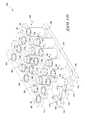
- FIGS. 1-3An example prior art cross-point memory array 5 is shown in FIGS. 1-3 ; with FIG. 1 being a top view, and with FIGS. 2 and 3 being cross-sectional side views.
- the cross-sectional views of FIGS. 2 and 3like all other cross-sectional views in this disclosure, only show features within the planes of the cross-sections. The cross-sectional views do not show materials behind the planes of the cross-sections in order to simplify the drawings.
- the top view of FIG. 1shows that the memory array comprises a plurality of global bitlines 10 - 14 that extend along a first horizontal direction, and comprises a plurality of wordlines 20 - 25 that extend orthogonally to the global bitlines.
- the cross-sectional side view of FIG. 2shows that the wordlines of FIG. 1 are actually the top series of a stack of wordlines, with FIG. 2 showing two underlying series of wordlines.
- the wordlines within one of the underlying seriesare labeled as wordlines 20 a - 25 a
- the wordlines in the other of the underlying seriesare labeled as wordlines 20 b - 25 b.
- Eighteen wordlines( 20 - 25 , 20 a - 25 a and 20 b - 25 b ) are shown in the cross-sectional view of FIG. 2 .
- the eighteen wordlinesform a two-dimensional wordline array having columns of three wordlines, and rows of six wordlines.
- FIGS. 1-3show that vertical bitline pillars 30 - 44 extend upwardly from the global bitlines.
- the bitline pillarsextend through the wordline array, and are between some of the columns of such wordline array.
- the wordlines, bitlines and vertical bitline pillarscomprise electrically conductive material, such as, for example, one or more of various metals, metal-containing compositions, and conductively-doped semiconductor materials.
- Memory cell material 45(only some of which is labeled) is provided between the wordlines and vertical bitline pillars; and access devices 46 (only some of which are labeled) are provided between the wordlines and the vertical bitline pillars.
- the memory cell material and access device provided between a wordline and a vertical bitline pillartogether form a memory cell 47 (only some of which are labeled).
- the memory cell materialis shown to be a single homogeneous composition, it may comprise multiple discrete compositions in some applications.
- the access devicesare shown to comprise single, homogeneous compositions, the access devices may comprise numerous discrete compositions; and often do comprise two or more different materials.
- only a single access deviceis shown in each memory cell, there can be multiple access devices in the individual memory cells.
- the memory cell materialis shown directly adjacent the vertical bitline pillars, and the access devices are shown directly adjacent the wordlines, the relative orientations of the memory cell material and the access devices may be reversed.
- each individual memory cellmay be uniquely addressed by a combination of a global bitline and a wordline.
- a voltage differential between global bitline 12 and wordline 20may be utilized to access the memory cell located at the intersection where wordline 20 crosses vertical bitline pillar 36 .
- Such accessmay be utilized for writing to the memory cell by placing the memory cell in a specific data storage state, and for reading from the memory cell by ascertaining which data storage state the memory cell is in.
- the wordlines within the two-dimensional wordline array of FIG. 2may be considered to be arranged in a plurality of elevational planes 50 - 52 , and accordingly the top view of FIG. 1 may be considered to be showing the uppermost elevational plane 52 of the wordline array.
- the memory arraymay be considered to also comprise the elevational planes 50 - 52 , and each memory unit of the memory array may be considered to have an area along the elevational plane containing such memory unit.
- the areamay be stated in terms of a minimum feature size, F, utilized to form the memory array.
- Such minimum feature sizewill be the widths of the bitlines, the widths of the wordlines, the widths of the vertical bitline pillars, and the widths of the spaces between the bitlines and the wordlines if the memory array is fabricated to its absolute minimum dimensions.
- FIG. 1shows a square perimeter around one of the memory units. Such perimeter has sides that are of dimension 2F, and accordingly the memory unit has an area along elevational plane 52 of about 4F 2 .
- the areais referred to as being “about 4F 2 ,” rather than as being absolutely 4F 2 because the illustrated perimeter assumes that the memory cell material 45 and access device 46 are of negligible size. Since the memory cell material 45 and access device 46 have some physical dimension, the planar area of the memory unit cell will approach 4F 2 , but will not be 4F 2 in an absolute mathematical sense.
- each memory cell unitmay be considered to be 4F 2 in a context in which the memory cell material and access device are ignored; or in other words may be considered to be 4F 2 relative to the wordlines, bitlines and spaces consumed by each memory cell unit.
- FIGS. 1-3are diagrammatic views of a portion of a prior art memory array.
- FIG. 1is a top view of the array, and
- FIGS. 2 and 3are diagrammatic cross-sectional side views along the lines 2 - 2 and 3 - 3 , respectively, of FIG. 1 .
- FIGS. 4-6are diagrammatic views of a portion of an example embodiment memory array.
- FIG. 4is a top view of the array, and
- FIGS. 5 and 6are diagrammatic cross-sectional side views along the lines 5 - 5 and 6 - 6 , respectively, of FIG. 4 .
- FIG. 7is a three-dimensional view of a memory array similar to that of FIGS. 4-6 .
- FIG. 8is a diagrammatic cross-sectional view similar to that of FIG. 5 , and shows another example embodiment memory array.
- FIG. 9is a three-dimensional view of another example embodiment memory array.
- FIG. 10is a three-dimensional view of another example embodiment memory array.
- Some embodimentsinclude new memory arrays in which cross-point memory cells may be more tightly packed than is achieved with conventional memory arrays. Example embodiments are described with reference to FIGS. 4-10 .
- FIGS. 4-6An example embodiment memory array 100 is shown in FIGS. 4-6 .
- the top view of FIG. 4shows that the memory array 100 comprises a plurality of global bitlines 110 - 118 that extend along a first horizontal direction, and comprises a plurality of wordlines 120 - 125 that extend orthogonally to the global bitlines.
- the cross-sectional side view of FIG. 5shows that the wordlines of FIG. 4 are actually the top series of a stack of wordlines, with FIG. 5 showing two underlying series of wordlines; with the wordlines within one of the series being labeled as wordlines 120 a - 125 a , and with the wordlines in the other series being labeled as wordlines 120 b - 125 b .
- the eighteen wordlinesform a two-dimensional wordline array having columns of three wordlines, and rows of six wordlines.
- the two-dimensional wordline arrayis one example of a diversity of different two-dimensional wordline arrays.
- Such wordline arrayswill generally have at least two wordlines in each row of the array, and at least two wordlines in each column of the arrays.
- FIGS. 4-6show that vertical bitline pillars 160 - 182 extend upwardly from the global bitlines.
- the bitline pillarsextend through the wordline array, and are between adjacent columns of such wordline array.
- the wordlines, bitlines and vertical bitline pillarscomprise electrically conductive material, such as, for example, one or more of various metals, metal-containing compositions, and conductively-doped semiconductor materials.
- Memory cell material 45(only some of which is labeled) is provided between the wordlines and vertical bitline pillars; and access devices 46 (only some of which are labeled) are provided between the wordlines and the vertical bitline pillars.
- the memory cell material and access device provided between a wordline and a vertical bitline pillartogether form a memory cell 47 (only some of which are labeled).
- the memory cell material 45 and access devices 46 of the example embodiment of FIGS. 4-6may be the same as the memory cell material 45 and access devices 46 of the prior art described above in the “Background” section.
- the memory cell materialis shown to be a single homogeneous composition, it may comprise multiple discrete compositions in some applications.
- the access devicesare shown to comprise single, homogeneous compositions, the access devices may comprise numerous discrete compositions; and often do comprise two or more different materials.
- only a single access deviceis shown in each memory cell, there may be multiple access devices in the individual memory cells.
- the memory cell materialis shown adjacent the vertical bitline pillar, and the access device is shown adjacent the wordline, the relative orientations of the memory cell material and the access device may be reversed.
- the cross-sectional view of FIG. 6shows that some of the global bitlines 110 - 118 are formed at a different elevational level than others of the global bitlines.
- the global bitlinesinclude a first series containing bitlines 110 , 112 , 114 , 116 and 118 that is formed at one elevational level, and a second series containing bitlines 111 , 113 , 115 and 117 that is formed at a different elevational level.
- the global bitlines of the first seriesalternate with those of the second series, as shown in FIG. 6 .
- each individual memory cellmay be uniquely addressed by a combination of a global bitline and a wordline.
- a voltage differential between global bitline 116 and wordline 121may be utilized to access the memory cell located at the intersection where wordline 121 crosses vertical bitline pillar 175 .
- Such accessmay be utilized for writing to the memory cell by placing the memory cell in a specific data storage state, and for reading from the memory cell by ascertaining which data storage state the memory cell is in.
- the wordlines within the two-dimensional wordline array of FIG. 5may be considered to be arranged in a plurality of elevational planes 150 - 152 , and accordingly the top view of FIG. 4 may be considered to be showing the uppermost elevational plane 152 of the wordline array.
- the memory arraymay be considered to also comprise the elevational planes 150 - 152 , and each memory unit of the memory array may be considered to have an area along the elevational plane containing such memory unit.
- the areamay be stated in terms of the minimum feature size, F, utilized to form the memory array.
- Such minimum feature sizewill be the widths of the bitlines, the widths of the wordlines, the widths of the vertical bitline pillars, and the widths of the spaces between the bitlines and wordlines if the memory array is fabricated to its absolute minimum dimensions.
- the top view of FIG. 4shows a rectangular perimeter around one of the memory units of the example embodiment memory array.
- Such perimeterhas two sides that are of dimension 2F, and two sides that are of dimension F.
- the memory unithas an area along elevational plane 152 of about 2F 2 .
- the areais referred to as being “about 2F 2 ,” rather than as being absolutely 2F 2 because the illustrated perimeter assumes that the memory cell material 45 and access device 46 are of negligible size. Since the memory cell material 45 and access device 46 have some physical dimension, the planar area of the memory unit cell will approach 2F 2 , but will not be 2F 2 in an absolute mathematical sense. Alternatively, the planar area of each memory cell unit may be considered to be 2F 2 if the memory cell material and access device are ignored; or in other words may be considered to be 2F 2 relative to the wordlines, bitlines and spaces consumed by each memory cell unit.
- FIG. 7is a three-dimensional view of an example embodiment memory array analogous to that of FIGS. 4-6 , which may assist the reader in visualizing such memory array. Identical number is utilized to label the components of FIG. 7 as was used to label the components of FIGS. 4-6 .
- the locations of the wordlines 120 - 125are indicated with arrows, but the wordlines are not shown in order to simplify the drawing.
- FIG. 7differs from that of FIGS. 4-6 in that the memory cell material 45 is contiguous around the vertical bitline pillars of FIG. 7 , and is not contiguous around such vertical pillars in the embodiment of FIGS. 4-6 . Accordingly, FIG. 7 shows a slightly different embodiment than FIGS. 4-6 .
- the embodiment of FIG. 7also shows the access devices 46 comprising material that is contiguous around the vertical bitline pillars.
- the memory cell materialmay be contiguous around the vertical pillars, but the material of the access devices may be discontinuous around such pillars.
- FIGS. 4-7have access devices 46 adjacent memory cell material 45 in the individual memory cells 47 of the memory array.
- each memory cell unitcomprises memory cell material and an access device.
- the access devicesmay be removed from the individual memory cell units to further reduce the size of the memory cell units.
- the access devicesmay be placed in locations between the vertical pillars and the global bitlines, rather than being placed in the individual memory cell units. Accordingly, while the cross-section of FIG.
- FIG. 5shows an embodiment in which the vertical bitline pillars 170 - 172 are ohmically connected to the global bitline 114 , in other embodiments such vertical bitline pillars may be connected to the global bitline through access devices that respond non-linearly to increasing voltage (such as, for example, ovonic threshold switches).
- FIG. 8shows a cross-sectional view analogous to that of FIG. 5 , but shows an embodiment in which a memory array 100 a has access devices 46 placed directly between the global bitline 114 and the vertical bitline pillars 170 - 172 .
- the embodiment of FIG. 8advantageously reduces the size of the memory cells 47 by removing the access devices from such memory cells.
- the only material between the wordlines (for instance, 120 - 125 ) and the vertical bitline pillars (for instance, 170 - 172 )is the memory cell material 45 .
- FIGS. 4-7show embodiments in which all of the global bitlines are on the same side of the two-dimensional wordline array (specifically, the two dimensional array comprising the wordlines 120 - 125 , 120 a - 125 a and 120 b - 125 b shown in FIG. 5 ). In other embodiments, some of the global bitlines may be on an opposite side of the wordline array relative to others of the global bitlines.
- FIG. 9shows a three-dimensional view of a memory array 200 in which the some of the global bitlines are one side of a two-dimensional wordline array, and others of the global bitlines are on an opposing side of the wordline array. Identical numbering will be used to describe FIG. 9 as is utilized above for describing FIGS. 4-7 .
- the wordlines 120 - 125 , 120 a - 125 a and 120 b - 125 bare not all shown in FIG. 9 in order to simplify the drawing. Instead, only wordlines 121 , 121 a and 121 b are shown, and the locations of wordlines 120 , 122 , 123 , 124 and 125 are indicated with arrows.
- the embodiment of FIG. 9may be considered to have some of the global bitlines 110 - 118 formed at a different elevational level than others of the global bitlines.
- the global bitlinesinclude a first series containing bitlines 112 , 114 and 116 that is formed at one elevational level (and specifically, below the wordlines in the shown embodiment), and a second series containing bitlines 111 , 113 , 115 and 117 that is formed at a different elevational level (and specifically, above the wordlines in the shown embodiment).
- the global bitlines of the first seriesalternate with those of the second series, as shown in FIG. 9 .
- the global bitlines of the first seriesare horizontally offset from the global bitlines of the second series, so that the global bitlines of the first series are not directly over the global bitlines of the second series.
- the global bitlines of the first seriesmay be directly over the global bitlines of the second series, as shown in FIG. 10 with reference to a memory array 300 .
- the wordlinesare not shown in FIG. 10 in order to simplify the drawing. However, locations of wordlines 120 - 125 are indicated with arrows.
- FIGS. 9 and 10may, like the embodiment of FIGS. 4-6 , form an array in which the planar area of individual memory cell units is 2F 2 relative to the wordlines, bitlines and spaces consumed by the individual memory cell units.
- the access devicesmay be in the memory cells of the embodiments of FIGS. 9 and 10 as shown, or may be between the vertical bitline pillars and the global bitlines in other embodiments analogous to the embodiment of FIG. 8 .
- a global bitline and the vertical pillars attached theretomay be considered to form a structure analogous to a comb.
- such combsmay be considered to be within two series that are elevationally offset relative to one another; with one series comprising global bitlines 110 , 112 , 114 , 116 and 118 , and the other series comprising global bitlines 111 , 113 , 115 and 117 .
- the combs of both seriesare parallel to one another and all have the vertical pillars extending in the same direction.
- one series of combshas the vertical pillars extending upwardly, while the other series of combs has the vertical pillars extending downwardly.
- the embodiment of FIG. 10has global bitlines 111 , 113 , 115 , and 117 within a first series of combs; and has global bitlines 112 , 114 , 116 and 118 within a second series of combs.
- the first seriesis exemplified by global bitline 118 and the vertical pillars 180 , 181 and 182 attached thereto; while the second series is exemplified by the combination of global bitline 117 and the vertical pillars 178 and 179 attached thereto.
- the first series of combshas vertical pillars extending upwardly, and the second series has vertical pillars extending downwardly.
- the memory arrays described hereinmay be incorporated into integrated circuitry, and thus may be supported by a semiconductor substrate in some applications.
- the memory arraysmay be formed by any suitable processing.
- first structureis over a second structure if the first structure is above the second structure regardless of any lateral displacement that may exist between the first and second structures; and a first structure is “directly over” a second structure if the first structure is vertically aligned with the second structure.
- the embodiments discussed abovemay be utilized in electronic systems, such as, for example, computers, cars, airplanes, clocks, cellular phones, etc.
Landscapes
- Physics & Mathematics (AREA)
- Engineering & Computer Science (AREA)
- Microelectronics & Electronic Packaging (AREA)
- Condensed Matter Physics & Semiconductors (AREA)
- General Physics & Mathematics (AREA)
- Chemical & Material Sciences (AREA)
- Crystallography & Structural Chemistry (AREA)
- High Energy & Nuclear Physics (AREA)
- Semiconductor Memories (AREA)
Abstract
Description
Claims (12)
Priority Applications (18)
| Application Number | Priority Date | Filing Date | Title |
|---|---|---|---|
| US12/795,565US8289763B2 (en) | 2010-06-07 | 2010-06-07 | Memory arrays |
| CN201180027954.6ACN102939632B (en) | 2010-06-07 | 2011-05-06 | Memory arrays |
| KR1020127031988AKR101417568B1 (en) | 2010-06-07 | 2011-05-06 | Memory arrays |
| EP11792836.6AEP2577668B1 (en) | 2010-06-07 | 2011-05-06 | Memory arrays |
| PCT/US2011/035601WO2011156069A2 (en) | 2010-06-07 | 2011-05-06 | Memory arrays |
| SG2012089520ASG186189A1 (en) | 2010-06-07 | 2011-05-06 | Memory arrays |
| JP2013514178AJP5549962B2 (en) | 2010-06-07 | 2011-05-06 | Memory array. |
| TW100119681ATWI517304B (en) | 2010-06-07 | 2011-06-03 | Memory arrays |
| US13/607,681US8488374B2 (en) | 2010-06-07 | 2012-09-08 | Memory arrays |
| US13/937,994US9412421B2 (en) | 2010-06-07 | 2013-07-09 | Memory arrays |
| US15/220,316US9697873B2 (en) | 2010-06-07 | 2016-07-26 | Memory arrays |
| US15/639,423US9887239B2 (en) | 2010-06-07 | 2017-06-30 | Memory arrays |
| US15/855,939US9989616B2 (en) | 2010-06-07 | 2017-12-27 | Memory arrays |
| US15/996,733US10241185B2 (en) | 2010-06-07 | 2018-06-04 | Memory arrays |
| US16/280,588US10613184B2 (en) | 2010-06-07 | 2019-02-20 | Memory arrays |
| US16/799,670US10656231B1 (en) | 2010-06-07 | 2020-02-24 | Memory Arrays |
| US16/850,293US10746835B1 (en) | 2010-06-07 | 2020-04-16 | Memory arrays |
| US16/924,068US10859661B2 (en) | 2010-06-07 | 2020-07-08 | Memory arrays |
Applications Claiming Priority (1)
| Application Number | Priority Date | Filing Date | Title |
|---|---|---|---|
| US12/795,565US8289763B2 (en) | 2010-06-07 | 2010-06-07 | Memory arrays |
Related Child Applications (1)
| Application Number | Title | Priority Date | Filing Date |
|---|---|---|---|
| US13/607,681DivisionUS8488374B2 (en) | 2010-06-07 | 2012-09-08 | Memory arrays |
Publications (2)
| Publication Number | Publication Date |
|---|---|
| US20110299328A1 US20110299328A1 (en) | 2011-12-08 |
| US8289763B2true US8289763B2 (en) | 2012-10-16 |
Family
ID=45064357
Family Applications (11)
| Application Number | Title | Priority Date | Filing Date |
|---|---|---|---|
| US12/795,565Expired - Fee RelatedUS8289763B2 (en) | 2010-06-07 | 2010-06-07 | Memory arrays |
| US13/607,681Expired - Fee RelatedUS8488374B2 (en) | 2010-06-07 | 2012-09-08 | Memory arrays |
| US13/937,994Expired - Fee RelatedUS9412421B2 (en) | 2010-06-07 | 2013-07-09 | Memory arrays |
| US15/220,316Expired - Fee RelatedUS9697873B2 (en) | 2010-06-07 | 2016-07-26 | Memory arrays |
| US15/639,423ActiveUS9887239B2 (en) | 2010-06-07 | 2017-06-30 | Memory arrays |
| US15/855,939ActiveUS9989616B2 (en) | 2010-06-07 | 2017-12-27 | Memory arrays |
| US15/996,733ActiveUS10241185B2 (en) | 2010-06-07 | 2018-06-04 | Memory arrays |
| US16/280,588Expired - Fee RelatedUS10613184B2 (en) | 2010-06-07 | 2019-02-20 | Memory arrays |
| US16/799,670Expired - Fee RelatedUS10656231B1 (en) | 2010-06-07 | 2020-02-24 | Memory Arrays |
| US16/850,293Expired - Fee RelatedUS10746835B1 (en) | 2010-06-07 | 2020-04-16 | Memory arrays |
| US16/924,068Expired - Fee RelatedUS10859661B2 (en) | 2010-06-07 | 2020-07-08 | Memory arrays |
Family Applications After (10)
| Application Number | Title | Priority Date | Filing Date |
|---|---|---|---|
| US13/607,681Expired - Fee RelatedUS8488374B2 (en) | 2010-06-07 | 2012-09-08 | Memory arrays |
| US13/937,994Expired - Fee RelatedUS9412421B2 (en) | 2010-06-07 | 2013-07-09 | Memory arrays |
| US15/220,316Expired - Fee RelatedUS9697873B2 (en) | 2010-06-07 | 2016-07-26 | Memory arrays |
| US15/639,423ActiveUS9887239B2 (en) | 2010-06-07 | 2017-06-30 | Memory arrays |
| US15/855,939ActiveUS9989616B2 (en) | 2010-06-07 | 2017-12-27 | Memory arrays |
| US15/996,733ActiveUS10241185B2 (en) | 2010-06-07 | 2018-06-04 | Memory arrays |
| US16/280,588Expired - Fee RelatedUS10613184B2 (en) | 2010-06-07 | 2019-02-20 | Memory arrays |
| US16/799,670Expired - Fee RelatedUS10656231B1 (en) | 2010-06-07 | 2020-02-24 | Memory Arrays |
| US16/850,293Expired - Fee RelatedUS10746835B1 (en) | 2010-06-07 | 2020-04-16 | Memory arrays |
| US16/924,068Expired - Fee RelatedUS10859661B2 (en) | 2010-06-07 | 2020-07-08 | Memory arrays |
Country Status (8)
| Country | Link |
|---|---|
| US (11) | US8289763B2 (en) |
| EP (1) | EP2577668B1 (en) |
| JP (1) | JP5549962B2 (en) |
| KR (1) | KR101417568B1 (en) |
| CN (1) | CN102939632B (en) |
| SG (1) | SG186189A1 (en) |
| TW (1) | TWI517304B (en) |
| WO (1) | WO2011156069A2 (en) |
Cited By (7)
| Publication number | Priority date | Publication date | Assignee | Title |
|---|---|---|---|---|
| US9184218B2 (en) | 2013-10-14 | 2015-11-10 | Samsung Electronics Co., Ltd. | Semiconductor memory device having three-dimensional cross point array |
| US9230644B2 (en)* | 2014-04-28 | 2016-01-05 | SK Hynix Inc. | Electronic device |
| US11475947B1 (en) | 2021-04-15 | 2022-10-18 | Micron Technology, Inc. | Decoding architecture for memory tiles |
| US11574957B2 (en) | 2018-10-10 | 2023-02-07 | Micron Technology, Inc. | Three-dimensional memory array |
| US11587606B2 (en) | 2021-04-15 | 2023-02-21 | Micron Technology, Inc. | Decoding architecture for memory devices |
| US11894103B2 (en) | 2021-04-15 | 2024-02-06 | Micron Technology, Inc. | Decoding architecture for word line tiles |
| US12356635B2 (en) | 2021-05-26 | 2025-07-08 | Samsung Electronics Co., Ltd. | Three-dimensional memory device including a variable resistance memory |
Families Citing this family (22)
| Publication number | Priority date | Publication date | Assignee | Title |
|---|---|---|---|---|
| US8289763B2 (en) | 2010-06-07 | 2012-10-16 | Micron Technology, Inc. | Memory arrays |
| CN102881317B (en)* | 2011-07-13 | 2015-08-12 | 华邦电子股份有限公司 | 3D memory array |
| US8835990B2 (en)* | 2011-08-12 | 2014-09-16 | Winbond Electronics Corp. | 3D memory array |
| KR101957897B1 (en)* | 2012-04-26 | 2019-03-13 | 에스케이하이닉스 주식회사 | Resistance variable memory device and method for fabricating the same |
| US8841649B2 (en) | 2012-08-31 | 2014-09-23 | Micron Technology, Inc. | Three dimensional memory array architecture |
| US8729523B2 (en)* | 2012-08-31 | 2014-05-20 | Micron Technology, Inc. | Three dimensional memory array architecture |
| KR20140054975A (en)* | 2012-10-30 | 2014-05-09 | 에스케이하이닉스 주식회사 | Variable resistance memory device |
| KR20140113024A (en)* | 2013-03-15 | 2014-09-24 | 에스케이하이닉스 주식회사 | Resistance variable Memory Device And Method of Driving The Same |
| US9728584B2 (en) | 2013-06-11 | 2017-08-08 | Micron Technology, Inc. | Three dimensional memory array with select device |
| US9236124B2 (en) | 2014-03-07 | 2016-01-12 | Kabushiki Kaisha Toshiba | Nonvolatile memory device |
| KR102203459B1 (en) | 2014-08-11 | 2021-01-15 | 삼성전자주식회사 | Semiconductor device |
| EP3389199A4 (en)* | 2015-12-30 | 2018-11-21 | Huawei Technologies Co., Ltd. | Bi-directional optical sub-assembly |
| US9837471B2 (en) | 2016-04-14 | 2017-12-05 | Western Digital Technologies, Inc. | Dual OTS memory cell selection means and method |
| US10269804B2 (en) | 2016-05-11 | 2019-04-23 | Micron Technology, Inc. | Array of cross point memory cells and methods of forming an array of cross point memory cells |
| KR102673120B1 (en)* | 2016-12-05 | 2024-06-05 | 삼성전자주식회사 | Semiconductor device and method for fabricating the same |
| KR102345542B1 (en)* | 2017-06-02 | 2021-12-30 | 삼성전자주식회사 | Semiconductor device having variable resistor memory device |
| US10461125B2 (en) | 2017-08-29 | 2019-10-29 | Micron Technology, Inc. | Three dimensional memory arrays |
| US10700128B1 (en) | 2018-12-21 | 2020-06-30 | Micron Technology, Inc. | Three-dimensional memory array |
| KR102683677B1 (en)* | 2019-07-12 | 2024-07-11 | 에스케이하이닉스 주식회사 | Vertical memory device |
| US11716914B2 (en)* | 2020-11-11 | 2023-08-01 | Globalfoundries Singapore Pte. Ltd. | Non-volatile memory device with filament confinement |
| CN117881189A (en) | 2020-11-13 | 2024-04-12 | 武汉新芯集成电路制造有限公司 | Semiconductor device with a semiconductor layer having a plurality of semiconductor layers |
| US20240087959A1 (en)* | 2022-09-08 | 2024-03-14 | Taiwan Semiconductor Manufacturing Company Ltd. | Semiconductor structure and method of manufacturing the same |
Citations (13)
| Publication number | Priority date | Publication date | Assignee | Title |
|---|---|---|---|---|
| US20020018355A1 (en) | 1998-11-16 | 2002-02-14 | Johnson Mark G. | Vertically stacked field programmable nonvolatile memory and method of fabrication |
| US20040245547A1 (en) | 2003-06-03 | 2004-12-09 | Hitachi Global Storage Technologies B.V. | Ultra low-cost solid-state memory |
| US20050001257A1 (en) | 2003-02-14 | 2005-01-06 | Till Schloesser | Method of fabricating and architecture for vertical transistor cells and transistor-controlled memory cells |
| US6961258B2 (en) | 2001-06-30 | 2005-11-01 | Ovonyx, Inc. | Pore structure for programmable device |
| US7009278B2 (en) | 2003-11-24 | 2006-03-07 | Sharp Laboratories Of America, Inc. | 3d rram |
| US20070278578A1 (en) | 2005-02-18 | 2007-12-06 | Fujitsu Limited | Memory cell array, method of producing the same, and semiconductor memory device using the same |
| US7388775B2 (en) | 2005-03-30 | 2008-06-17 | Ovonyx, Inc. | Detecting switching of access elements of phase change memory cells |
| US20080175031A1 (en) | 2007-01-23 | 2008-07-24 | Samsung Electronics Co., Ltd. | Memory cell of a resistive semiconductor memory device, a resistive semiconductor memory device having a three-dimensional stack structure, and related methods |
| US20090059644A1 (en) | 2007-08-29 | 2009-03-05 | Elpida Memory, Inc. | Semiconductor memory device having vertical transistors |
| US7570511B2 (en) | 2006-11-10 | 2009-08-04 | Samsung Electronics Co., Ltd. | Semiconductor memory device having a three-dimensional cell array structure |
| US20110261607A1 (en)* | 2010-04-22 | 2011-10-27 | Micron Technology, Inc. | Arrays Of Vertically Stacked Tiers Of Non-Volatile Cross Point Memory Cells, Methods Of Forming Arrays Of Vertically Stacked Tiers Of Non-Volatile Cross Point Memory Cells, And Methods Of Reading A Data Value Stored By An Array Of Vertically Stacked Tiers Of Non-Volatile Cross Point Memory Cells |
| US20110261606A1 (en)* | 2010-04-22 | 2011-10-27 | Sandhu Gurtej S | Arrays Of Vertically Stacked Tiers Of Non-Volatile Cross Point Memory Cells, Methods Of Forming Arrays Of Vertically Stacked Tiers Of Non-Volatile Cross Point Memory Cells, And Methods Of Reading A Data Value Stored By An Array Of Vertically Stacked Tiers Of Non-Volatile Cross Point Memory Cells |
| WO2011156069A2 (en) | 2010-06-07 | 2011-12-15 | Micron Technology, Inc. | Memory arrays |
Family Cites Families (278)
| Publication number | Priority date | Publication date | Assignee | Title |
|---|---|---|---|---|
| BE713483A (en) | 1968-04-10 | 1968-08-16 | ||
| GB1266513A (en) | 1969-05-19 | 1972-03-08 | ||
| AU562641B2 (en) | 1983-01-18 | 1987-06-18 | Energy Conversion Devices Inc. | Electronic matrix array |
| US4616392A (en) | 1984-10-04 | 1986-10-14 | Westinghouse Electric Corp. | Bladder mandrel for hydraulic expansions of tubes and sleeves |
| US4715685A (en) | 1985-03-04 | 1987-12-29 | Energy Conversion Devices, Inc. | Liquid crystal display having potential source in a diode ring |
| JPH01130552A (en) | 1987-11-17 | 1989-05-23 | Sharp Corp | high resistance element |
| US4964080A (en) | 1990-03-09 | 1990-10-16 | Intel Corporation | Three-dimensional memory cell with integral select transistor |
| US5057888A (en) | 1991-01-28 | 1991-10-15 | Micron Technology, Inc. | Double DRAM cell |
| US6432767B2 (en) | 1995-12-05 | 2002-08-13 | Hitachi, Ltd. | Method of fabricating semiconductor device |
| US6271131B1 (en) | 1998-08-26 | 2001-08-07 | Micron Technology, Inc. | Methods for forming rhodium-containing layers such as platinum-rhodium barrier layers |
| US6197628B1 (en) | 1998-08-27 | 2001-03-06 | Micron Technology, Inc. | Ruthenium silicide diffusion barrier layers and methods of forming same |
| US6034882A (en) | 1998-11-16 | 2000-03-07 | Matrix Semiconductor, Inc. | Vertically stacked field programmable nonvolatile memory and method of fabrication |
| US6635914B2 (en) | 2000-09-08 | 2003-10-21 | Axon Technologies Corp. | Microelectronic programmable device and methods of forming and programming the same |
| US6218696B1 (en) | 1999-06-07 | 2001-04-17 | Infineon Technologies North America Corp. | Layout and wiring scheme for memory cells with vertical transistors |
| US20040124407A1 (en) | 2000-02-11 | 2004-07-01 | Kozicki Michael N. | Scalable programmable structure, an array including the structure, and methods of forming the same |
| US7247876B2 (en) | 2000-06-30 | 2007-07-24 | Intel Corporation | Three dimensional programmable device and method for fabricating the same |
| US6451646B1 (en) | 2000-08-30 | 2002-09-17 | Micron Technology, Inc. | High-k dielectric materials and processes for manufacturing them |
| US7067852B1 (en) | 2000-09-12 | 2006-06-27 | National Semiconductor Corporation | Electrostatic discharge (ESD) protection structure |
| KR100451096B1 (en) | 2000-09-19 | 2004-10-02 | 엔이씨 일렉트로닉스 가부시키가이샤 | Non-volatile semiconductor memory device with magnetic memory cell array |
| EP1331671B1 (en) | 2000-11-01 | 2007-01-24 | Japan Science and Technology Agency | Point contact array and electronic circuit comprising the same |
| US6534357B1 (en) | 2000-11-09 | 2003-03-18 | Micron Technology, Inc. | Methods for forming conductive structures and structures regarding same |
| US6646297B2 (en) | 2000-12-26 | 2003-11-11 | Ovonyx, Inc. | Lower electrode isolation in a double-wide trench |
| US6524867B2 (en) | 2000-12-28 | 2003-02-25 | Micron Technology, Inc. | Method for forming platinum-rhodium stack as an oxygen barrier |
| US6440753B1 (en) | 2001-01-24 | 2002-08-27 | Infineon Technologies North America Corp. | Metal hard mask for ILD RIE processing of semiconductor memory devices to prevent oxidation of conductive lines |
| JP4818519B2 (en) | 2001-02-06 | 2011-11-16 | ルネサスエレクトロニクス株式会社 | Magnetic storage |
| US7102150B2 (en) | 2001-05-11 | 2006-09-05 | Harshfield Steven T | PCRAM memory cell and method of making same |
| ITMI20011150A1 (en) | 2001-05-30 | 2002-11-30 | St Microelectronics Srl | COLUMN MULTIPLATOR FOR SEMICONDUCTOR MEMORIES |
| US7193267B2 (en) | 2001-06-28 | 2007-03-20 | Sharp Laboratories Of America, Inc. | Cross-point resistor memory array |
| US6905937B2 (en) | 2001-06-28 | 2005-06-14 | Sharp Laboratories Of America, Inc. | Methods of fabricating a cross-point resistor memory array |
| US6693821B2 (en) | 2001-06-28 | 2004-02-17 | Sharp Laboratories Of America, Inc. | Low cross-talk electrically programmable resistance cross point memory |
| US6825058B2 (en) | 2001-06-28 | 2004-11-30 | Sharp Laboratories Of America, Inc. | Methods of fabricating trench isolated cross-point memory array |
| US6567301B2 (en) | 2001-08-09 | 2003-05-20 | Hewlett-Packard Development Company, L.P. | One-time programmable unit memory cell based on vertically oriented fuse and diode and one-time programmable memory using the same |
| US6946712B2 (en) | 2001-11-07 | 2005-09-20 | Kabushiki Kaisha Toshiba | Magnetic memory device using SOI substrate |
| US20030143853A1 (en) | 2002-01-31 | 2003-07-31 | Celii Francis G. | FeRAM capacitor stack etch |
| JP2003273252A (en) | 2002-03-12 | 2003-09-26 | Mitsubishi Electric Corp | Semiconductor storage device |
| US6778421B2 (en) | 2002-03-14 | 2004-08-17 | Hewlett-Packard Development Company, Lp. | Memory device array having a pair of magnetic bits sharing a common conductor line |
| US6687147B2 (en) | 2002-04-02 | 2004-02-03 | Hewlett-Packard Development Company, L.P. | Cubic memory array with diagonal select lines |
| JP4047615B2 (en) | 2002-04-03 | 2008-02-13 | 株式会社ルネサステクノロジ | Magnetic storage |
| US6757188B2 (en) | 2002-05-22 | 2004-06-29 | Hewlett-Packard Development Company, L.P. | Triple sample sensing for magnetic random access memory (MRAM) with series diodes |
| DE10223178B4 (en) | 2002-05-24 | 2004-11-04 | Infineon Technologies Ag | Circuit arrangement with a sequence control, integrated memory and test arrangement with such a circuit arrangement |
| US6952043B2 (en) | 2002-06-27 | 2005-10-04 | Matrix Semiconductor, Inc. | Electrically isolated pillars in active devices |
| TWI233204B (en) | 2002-07-26 | 2005-05-21 | Infineon Technologies Ag | Nonvolatile memory element and associated production methods and memory element arrangements |
| US6753561B1 (en) | 2002-08-02 | 2004-06-22 | Unity Semiconductor Corporation | Cross point memory array using multiple thin films |
| US6834008B2 (en) | 2002-08-02 | 2004-12-21 | Unity Semiconductor Corporation | Cross point memory array using multiple modes of operation |
| US7067862B2 (en) | 2002-08-02 | 2006-06-27 | Unity Semiconductor Corporation | Conductive memory device with conductive oxide electrodes |
| US6859382B2 (en) | 2002-08-02 | 2005-02-22 | Unity Semiconductor Corporation | Memory array of a non-volatile ram |
| US6970375B2 (en) | 2002-08-02 | 2005-11-29 | Unity Semiconductor Corporation | Providing a reference voltage to a cross point memory array |
| US6785159B2 (en) | 2002-08-29 | 2004-08-31 | Micron Technology, Inc. | Combination etch stop and in situ resistor in a magnetoresistive memory and methods for fabricating same |
| US7184301B2 (en) | 2002-11-27 | 2007-02-27 | Nec Corporation | Magnetic memory cell and magnetic random access memory using the same |
| WO2004061851A2 (en) | 2002-12-19 | 2004-07-22 | Matrix Semiconductor, Inc | An improved method for making high-density nonvolatile memory |
| US7005350B2 (en) | 2002-12-31 | 2006-02-28 | Matrix Semiconductor, Inc. | Method for fabricating programmable memory array structures incorporating series-connected transistor strings |
| DE10261457B3 (en) | 2002-12-31 | 2004-03-25 | Infineon Technologies Ag | Integrated circuit with transistor array of vertical FET selection transistors has array diagnosis test structure with two offset word, bit line combs alternately connecting different word, bit lines |
| JP2004220740A (en) | 2003-01-17 | 2004-08-05 | Seiko Epson Corp | Ferroelectric memory device |
| US6906937B1 (en) | 2003-03-21 | 2005-06-14 | Netlogic Microsystems, Inc. | Bit line control circuit for a content addressable memory |
| US6958273B2 (en) | 2003-03-21 | 2005-10-25 | Silicon Storage Technology, Inc. | Self-aligned method of forming a semiconductor memory array of floating gate memory cells with buried floating gate, pointed floating gate and pointed channel region, and a memory array made thereby |
| US6753562B1 (en) | 2003-03-27 | 2004-06-22 | Sharp Laboratories Of America, Inc. | Spin transistor magnetic random access memory device |
| US6879505B2 (en) | 2003-03-31 | 2005-04-12 | Matrix Semiconductor, Inc. | Word line arrangement having multi-layer word line segments for three-dimensional memory array |
| US7233024B2 (en)* | 2003-03-31 | 2007-06-19 | Sandisk 3D Llc | Three-dimensional memory device incorporating segmented bit line memory array |
| US7459715B2 (en) | 2003-04-03 | 2008-12-02 | Kabushiki Kaisha Toshiba | Resistance change memory device |
| WO2004090984A1 (en) | 2003-04-03 | 2004-10-21 | Kabushiki Kaisha Toshiba | Phase change memory device |
| US6806531B1 (en) | 2003-04-07 | 2004-10-19 | Silicon Storage Technology, Inc. | Non-volatile floating gate memory cell with floating gates formed in cavities, and array thereof, and method of formation |
| US7001846B2 (en) | 2003-05-20 | 2006-02-21 | Sharp Laboratories Of America, Inc. | High-density SOI cross-point memory array and method for fabricating same |
| TW589753B (en) | 2003-06-03 | 2004-06-01 | Winbond Electronics Corp | Resistance random access memory and method for fabricating the same |
| US7416911B2 (en) | 2003-06-24 | 2008-08-26 | California Institute Of Technology | Electrochemical method for attaching molecular and biomolecular structures to semiconductor microstructures and nanostructures |
| KR100507205B1 (en) | 2003-07-15 | 2005-08-10 | 현대자동차주식회사 | Knocking sensor mounting position determining method |
| US7029924B2 (en) | 2003-09-05 | 2006-04-18 | Sharp Laboratories Of America, Inc. | Buffered-layer memory cell |
| US6955992B2 (en) | 2003-09-30 | 2005-10-18 | Sharp Laboratories Of America, Inc. | One mask PT/PCMO/PT stack etching process for RRAM applications |
| WO2005041303A1 (en) | 2003-10-23 | 2005-05-06 | Matsushita Electric Industrial Co., Ltd. | Resistance change element, manufacturing method thereof, memory including the element, and drive method of the memory |
| US7098438B1 (en) | 2003-11-19 | 2006-08-29 | Raytheon Company | Method and apparatus for resetting a high speed latch circuit |
| JP4567963B2 (en) | 2003-12-05 | 2010-10-27 | ルネサスエレクトロニクス株式会社 | Semiconductor integrated circuit device |
| US6937507B2 (en) | 2003-12-05 | 2005-08-30 | Silicon Storage Technology, Inc. | Memory device and method of operating same |
| US6849891B1 (en) | 2003-12-08 | 2005-02-01 | Sharp Laboratories Of America, Inc. | RRAM memory cell electrodes |
| US7002197B2 (en) | 2004-01-23 | 2006-02-21 | Hewlett-Packard Development Company, L.P. | Cross point resistive memory array |
| US7138687B2 (en) | 2004-01-26 | 2006-11-21 | Macronix International Co., Ltd. | Thin film phase-change memory |
| US20060171200A1 (en) | 2004-02-06 | 2006-08-03 | Unity Semiconductor Corporation | Memory using mixed valence conductive oxides |
| US7538338B2 (en) | 2004-09-03 | 2009-05-26 | Unity Semiconductor Corporation | Memory using variable tunnel barrier widths |
| US7082052B2 (en) | 2004-02-06 | 2006-07-25 | Unity Semiconductor Corporation | Multi-resistive state element with reactive metal |
| US7050316B1 (en) | 2004-03-09 | 2006-05-23 | Silicon Storage Technology, Inc. | Differential non-volatile content addressable memory cell and array using phase changing resistor storage elements |
| US7476945B2 (en) | 2004-03-17 | 2009-01-13 | Sanyo Electric Co., Ltd. | Memory having reduced memory cell size |
| DE102004020297B4 (en) | 2004-04-26 | 2007-06-21 | Infineon Technologies Ag | Process for producing resistively switching memory components |
| DE102004026003B3 (en) | 2004-05-27 | 2006-01-19 | Infineon Technologies Ag | Resistive memory cell arrangement |
| JP4377751B2 (en) | 2004-06-10 | 2009-12-02 | シャープ株式会社 | Cross-point structure semiconductor memory device and manufacturing method thereof |
| KR100614240B1 (en) | 2004-06-10 | 2006-08-18 | 삼성전자주식회사 | Semiconductor device including field effect transistor and method for forming same |
| US7187201B1 (en) | 2004-06-24 | 2007-03-06 | Xilinx, Inc. | Programmable logic device suitable for implementation in molecular electronics |
| US7091091B2 (en) | 2004-06-28 | 2006-08-15 | Promos Technologies Inc. | Nonvolatile memory fabrication methods in which a dielectric layer underlying a floating gate layer is spaced from an edge of an isolation trench and/or an edge of the floating gate layer |
| KR20070028604A (en) | 2004-06-30 | 2007-03-12 | 코닌클리즈케 필립스 일렉트로닉스 엔.브이. | Electrical apparatus having a layer of conductive material contacted by nanowires and manufacturing method thereof |
| US7791141B2 (en) | 2004-07-09 | 2010-09-07 | International Business Machines Corporation | Field-enhanced programmable resistance memory cell |
| JP2006032729A (en) | 2004-07-16 | 2006-02-02 | Matsushita Electric Ind Co Ltd | Nonvolatile memory and manufacturing method thereof |
| JP4827074B2 (en) | 2004-07-22 | 2011-11-30 | シャープ株式会社 | High density SOI crosspoint memory array and method for manufacturing the same |
| US7180160B2 (en) | 2004-07-30 | 2007-02-20 | Infineon Technologies Ag | MRAM storage device |
| US20080008642A1 (en) | 2004-08-24 | 2008-01-10 | Osaka University | Process For Producing Aluminum Nitride Crystal And Aluminum Nitride Crystal Obtained Thereby |
| KR100568543B1 (en) | 2004-08-31 | 2006-04-07 | 삼성전자주식회사 | Manufacturing method of phase change memory device having small contact point |
| KR100645044B1 (en) | 2004-09-17 | 2006-11-10 | 삼성전자주식회사 | Programming Method of Nonvolatile Memory Device with High Reliability |
| US7205238B2 (en) | 2004-10-21 | 2007-04-17 | Sharp Laboratories Of America, Inc. | Chemical mechanical polish of PCMO thin films for RRAM applications |
| JP4687066B2 (en) | 2004-10-25 | 2011-05-25 | 株式会社デンソー | Power IC |
| US7189626B2 (en) | 2004-11-03 | 2007-03-13 | Micron Technology, Inc. | Electroless plating of metal caps for chalcogenide-based memory devices |
| US7035141B1 (en) | 2004-11-17 | 2006-04-25 | Spansion Llc | Diode array architecture for addressing nanoscale resistive memory arrays |
| US7608503B2 (en) | 2004-11-22 | 2009-10-27 | Macronix International Co., Ltd. | Side wall active pin memory and manufacturing method |
| JP5135798B2 (en) | 2004-12-27 | 2013-02-06 | 日本電気株式会社 | Switching element, switching element driving method, rewritable logic integrated circuit, and memory element |
| JP4578985B2 (en) | 2005-01-12 | 2010-11-10 | 日本車輌製造株式会社 | Extruded hollow profile and railway vehicle structure formed by the profile |
| US7046550B1 (en) | 2005-01-18 | 2006-05-16 | International Business Machines Corporation | Cross-point memory architecture with improved selectivity |
| US7208372B2 (en) | 2005-01-19 | 2007-04-24 | Sharp Laboratories Of America, Inc. | Non-volatile memory resistor cell with nanotip electrode |
| KR100682926B1 (en) | 2005-01-31 | 2007-02-15 | 삼성전자주식회사 | Nonvolatile Memory Device Using Resistor and Manufacturing Method Thereof |
| JP4462424B2 (en) | 2005-02-03 | 2010-05-12 | セイコーエプソン株式会社 | Semiconductor device |
| DE102005005938B4 (en) | 2005-02-09 | 2009-04-30 | Qimonda Ag | Resistive memory element with shortened erase time, method of manufacture and memory cell arrangement |
| KR100697282B1 (en) | 2005-03-28 | 2007-03-20 | 삼성전자주식회사 | Resistive memory cell, formation method thereof and resistor memory array using same |
| US8031509B2 (en) | 2008-12-19 | 2011-10-04 | Unity Semiconductor Corporation | Conductive metal oxide structures in non-volatile re-writable memory devices |
| US7323349B2 (en) | 2005-05-02 | 2008-01-29 | Sharp Laboratories Of America, Inc. | Self-aligned cross point resistor memory array |
| US7782650B2 (en) | 2005-05-09 | 2010-08-24 | Nantero, Inc. | Nonvolatile nanotube diodes and nonvolatile nanotube blocks and systems using same and methods of making same |
| US9196615B2 (en) | 2005-05-09 | 2015-11-24 | Nantero Inc. | Nonvolatile nanotube diodes and nonvolatile nanotube blocks and systems using same and methods of making same |
| US7585724B2 (en) | 2005-05-10 | 2009-09-08 | Elite Semiconductor Memory Technology, Inc. | FLASH memory device and method of manufacture |
| KR100655447B1 (en) | 2005-06-07 | 2006-12-08 | 삼성전자주식회사 | Nonvolatile Memory Device with Floating Gate and Formation Method |
| US7321130B2 (en) | 2005-06-17 | 2008-01-22 | Macronix International Co., Ltd. | Thin film fuse phase change RAM and manufacturing method |
| US7514288B2 (en) | 2005-06-17 | 2009-04-07 | Macronix International Co., Ltd. | Manufacturing methods for thin film fuse phase change ram |
| US7238994B2 (en) | 2005-06-17 | 2007-07-03 | Macronix International Co., Ltd. | Thin film plate phase change ram circuit and manufacturing method |
| US20070010082A1 (en) | 2005-07-05 | 2007-01-11 | Cay-Uwe Pinnow | Structure and method for manufacturing phase change memories with particular switching characteristics |
| US7446010B2 (en) | 2005-07-18 | 2008-11-04 | Sharp Laboratories Of America, Inc. | Metal/semiconductor/metal (MSM) back-to-back Schottky diode |
| CN101228091A (en) | 2005-07-22 | 2008-07-23 | 高通股份有限公司 | Support structures and methods for MEMS devices |
| US7521705B2 (en) | 2005-08-15 | 2009-04-21 | Micron Technology, Inc. | Reproducible resistance variable insulating memory devices having a shaped bottom electrode |
| JP4309877B2 (en) | 2005-08-17 | 2009-08-05 | シャープ株式会社 | Semiconductor memory device |
| US20070048990A1 (en) | 2005-08-30 | 2007-03-01 | Sharp Laboratories Of America, Inc. | Method of buffer layer formation for RRAM thin film deposition |
| KR100630437B1 (en) | 2005-08-31 | 2006-10-02 | 삼성전자주식회사 | Nonvolatile Organic Resistance Memory Device and Manufacturing Method Thereof |
| KR100665227B1 (en) | 2005-10-18 | 2007-01-09 | 삼성전자주식회사 | Phase change memory device and manufacturing method thereof |
| US7236389B2 (en) | 2005-11-17 | 2007-06-26 | Sharp Laboratories Of America, Inc. | Cross-point RRAM memory array having low bit line crosstalk |
| US8106375B2 (en) | 2005-11-30 | 2012-01-31 | The Trustees Of The University Of Pennsylvania | Resistance-switching memory based on semiconductor composition of perovskite conductor doped perovskite insulator |
| US7666526B2 (en) | 2005-11-30 | 2010-02-23 | The Trustees Of The University Of Pennsylvania | Non-volatile resistance-switching oxide thin film devices |
| US20070132049A1 (en) | 2005-12-12 | 2007-06-14 | Stipe Barry C | Unipolar resistance random access memory (RRAM) device and vertically stacked architecture |
| JP4054347B2 (en) | 2005-12-16 | 2008-02-27 | シャープ株式会社 | Nonvolatile semiconductor memory device |
| ATE480873T1 (en) | 2005-12-20 | 2010-09-15 | Nxp Bv | VERTICAL PHASE CHANGE STORAGE CELL AND PROCESS FOR PRODUCTION THEREOF |
| KR100655082B1 (en) | 2005-12-23 | 2006-12-08 | 삼성전자주식회사 | Phase change memory device and manufacturing method thereof |
| US7531825B2 (en) | 2005-12-27 | 2009-05-12 | Macronix International Co., Ltd. | Method for forming self-aligned thermal isolation cell for a variable resistance memory array |
| US7560337B2 (en) | 2006-01-09 | 2009-07-14 | Macronix International Co., Ltd. | Programmable resistive RAM and manufacturing method |
| KR101186293B1 (en) | 2006-01-19 | 2012-09-27 | 삼성전자주식회사 | Resistive RAM comprising varistor and method of operating the same |
| JP2007201081A (en) | 2006-01-25 | 2007-08-09 | Elpida Memory Inc | Semiconductor memory device |
| US7456421B2 (en) | 2006-01-30 | 2008-11-25 | Macronix International Co., Ltd. | Vertical side wall active pin structures in a phase change memory and manufacturing methods |
| KR100723420B1 (en) | 2006-02-20 | 2007-05-30 | 삼성전자주식회사 | Nonvolatile Memory Device Including Amorphous Alloy Oxide Layer |
| KR100707212B1 (en) | 2006-03-08 | 2007-04-13 | 삼성전자주식회사 | Nanowire memory device and method of manufacturing the same |
| KR100745764B1 (en) | 2006-03-09 | 2007-08-02 | 삼성전자주식회사 | Manufacturing Method of Nanowire Memory Device and Nanowire Formation Control System Used in the Method |
| KR101176543B1 (en) | 2006-03-10 | 2012-08-28 | 삼성전자주식회사 | Resistance Random Memory Device |
| US8395199B2 (en) | 2006-03-25 | 2013-03-12 | 4D-S Pty Ltd. | Systems and methods for fabricating self-aligned memory cell |
| US20070246795A1 (en) | 2006-04-20 | 2007-10-25 | Micron Technology, Inc. | Dual depth shallow trench isolation and methods to form same |
| KR101213702B1 (en) | 2006-04-21 | 2012-12-18 | 삼성전자주식회사 | Non-volatile memory device having a pair of fins between which a void is defined |
| US7606055B2 (en) | 2006-05-18 | 2009-10-20 | Micron Technology, Inc. | Memory architecture and cell design employing two access transistors |
| KR101206034B1 (en) | 2006-05-19 | 2012-11-28 | 삼성전자주식회사 | Nonvolatile memory device using oxygen-deficient metal oxide layer and the fabrication method |
| KR100833903B1 (en) | 2006-06-13 | 2008-06-03 | 광주과학기술원 | Non-volatile Memory, Manufacturing Method and Device Thereof |
| KR101159075B1 (en) | 2006-06-27 | 2012-06-25 | 삼성전자주식회사 | Variable resistance random access memory device comprising n+ interfacial layer |
| KR100818271B1 (en) | 2006-06-27 | 2008-03-31 | 삼성전자주식회사 | Threshold Switching Operation Method of Nonvolatile Memory Device Applying Pulse Voltage |
| US7569459B2 (en) | 2006-06-30 | 2009-08-04 | International Business Machines Corporation | Nonvolatile programmable resistor memory cell |
| US7696077B2 (en) | 2006-07-14 | 2010-04-13 | Micron Technology, Inc. | Bottom electrode contacts for semiconductor devices and methods of forming same |
| US7932548B2 (en) | 2006-07-14 | 2011-04-26 | 4D-S Pty Ltd. | Systems and methods for fabricating self-aligned memory cell |
| JP2008028228A (en) | 2006-07-24 | 2008-02-07 | Seiko Epson Corp | Variable resistance element and resistance change type memory device |
| CN101496173B (en) | 2006-07-27 | 2010-12-22 | 松下电器产业株式会社 | Nonvolatile semiconductor storage device and method for manufacturing same |
| KR101309111B1 (en) | 2006-07-27 | 2013-09-17 | 삼성전자주식회사 | Method for forming of poly-Si pattern and multi-layer cross point resistive memory device comprising poly-Si pattern and method for manufacturing the same |
| KR100749740B1 (en) | 2006-08-01 | 2007-08-17 | 삼성전자주식회사 | Manufacturing Method of Phase Change Memory Device |
| US7515454B2 (en) | 2006-08-02 | 2009-04-07 | Infineon Technologies Ag | CBRAM cell and CBRAM array, and method of operating thereof |
| US7727908B2 (en) | 2006-08-03 | 2010-06-01 | Micron Technology, Inc. | Deposition of ZrA1ON films |
| JP4344372B2 (en) | 2006-08-22 | 2009-10-14 | シャープ株式会社 | Semiconductor memory device and driving method thereof |
| KR100755409B1 (en) | 2006-08-28 | 2007-09-04 | 삼성전자주식회사 | How to Program a Resistive Memory Device |
| JP4823316B2 (en) | 2006-09-05 | 2011-11-24 | 富士通株式会社 | Writing method for nonvolatile semiconductor memory device |
| US7553758B2 (en) | 2006-09-18 | 2009-06-30 | Samsung Electronics Co., Ltd. | Method of fabricating interconnections of microelectronic device using dual damascene process |
| JP2008078404A (en) | 2006-09-21 | 2008-04-03 | Toshiba Corp | Semiconductor memory and manufacturing method thereof |
| US7751163B2 (en) | 2006-09-29 | 2010-07-06 | Qimonda Ag | Electric device protection circuit and method for protecting an electric device |
| US8058643B2 (en) | 2006-09-29 | 2011-11-15 | The Board Of Trustees Of The Leland Stanford Junior University | Electrochemical memory with internal boundary |
| KR100772904B1 (en) | 2006-10-02 | 2007-11-05 | 삼성전자주식회사 | Variable resistance memory device and manufacturing method thereof |
| KR100819099B1 (en) | 2006-10-02 | 2008-04-03 | 삼성전자주식회사 | Variable resistance semiconductor memory device |
| KR100858083B1 (en) | 2006-10-18 | 2008-09-10 | 삼성전자주식회사 | A phase change memory device having a large contact area between a lower electrode contact layer and a phase change layer and a method of manufacturing the same |
| US10134985B2 (en) | 2006-10-20 | 2018-11-20 | The Regents Of The University Of Michigan | Non-volatile solid state resistive switching devices |
| US20080102278A1 (en) | 2006-10-27 | 2008-05-01 | Franz Kreupl | Carbon filament memory and method for fabrication |
| KR100827661B1 (en) | 2006-10-31 | 2008-05-07 | 삼성전자주식회사 | Phase change memory device having a double bottom electrode and method of manufacturing the same |
| US7872900B2 (en) | 2006-11-08 | 2011-01-18 | Symetrix Corporation | Correlated electron memory |
| US7639523B2 (en) | 2006-11-08 | 2009-12-29 | Symetrix Corporation | Stabilized resistive switching memory |
| KR101196392B1 (en) | 2006-11-28 | 2012-11-02 | 삼성전자주식회사 | Non-volatile Memory Device and method of fabricating the same |
| US7864568B2 (en)* | 2006-12-07 | 2011-01-04 | Renesas Electronics Corporation | Semiconductor storage device |
| US7557424B2 (en) | 2007-01-03 | 2009-07-07 | International Business Machines Corporation | Reversible electric fuse and antifuse structures for semiconductor devices |
| EP2168298B1 (en) | 2007-01-04 | 2022-03-09 | Nokia Technologies Oy | Apparatus, methods and computer program products providing a common signaling entry for a modular control channel structure |
| JP5091491B2 (en) | 2007-01-23 | 2012-12-05 | 株式会社東芝 | Nonvolatile semiconductor memory device |
| KR100885184B1 (en) | 2007-01-30 | 2009-02-23 | 삼성전자주식회사 | Memory device having resistance characteristics that can be controlled independently by electric and magnetic fields, and method of operation thereof |
| US7800093B2 (en) | 2007-02-01 | 2010-09-21 | Qimonda North America Corp. | Resistive memory including buried word lines |
| US20080185687A1 (en) | 2007-02-07 | 2008-08-07 | Industry-University Cooperation Foundation Hanyang University | Memory device and method for fabricating the same |
| JP2008192995A (en) | 2007-02-07 | 2008-08-21 | Matsushita Electric Ind Co Ltd | RESISTANCE CHANGE ELEMENT, ITS MANUFACTURING METHOD, AND RESISTANCE CHANGE TYPE MEMORY USING THE SAME |
| CN101242707A (en) | 2007-02-07 | 2008-08-13 | 鸿富锦精密工业(深圳)有限公司 | Circuit board and its design method |
| JP5313171B2 (en) | 2007-02-21 | 2013-10-09 | レール・リキード−ソシエテ・アノニム・プール・レテュード・エ・レクスプロワタシオン・デ・プロセデ・ジョルジュ・クロード | Method for forming a ruthenium-based film on a substrate |
| JP4798793B2 (en) | 2007-02-27 | 2011-10-19 | ヤマハモーターパワープロダクツ株式会社 | Canister arrangement structure in power generator |
| US7382647B1 (en) | 2007-02-27 | 2008-06-03 | International Business Machines Corporation | Rectifying element for a crosspoint based memory array architecture |
| KR100852206B1 (en) | 2007-04-04 | 2008-08-13 | 삼성전자주식회사 | Resistive memory device and manufacturing method thereof. |
| US7723786B2 (en) | 2007-04-11 | 2010-05-25 | Ronald Kakoschke | Apparatus of memory array using FinFETs |
| US7755076B2 (en) | 2007-04-17 | 2010-07-13 | Macronix International Co., Ltd. | 4F2 self align side wall active phase change memory |
| US7569844B2 (en) | 2007-04-17 | 2009-08-04 | Macronix International Co., Ltd. | Memory cell sidewall contacting side electrode |
| CN100521278C (en) | 2007-04-19 | 2009-07-29 | 复旦大学 | Preparing method for RRAM to avoid forming phenomenon using CuxO as storage medium |
| JP4252624B2 (en)* | 2007-06-01 | 2009-04-08 | パナソニック株式会社 | Resistance change memory device |
| US7459716B2 (en) | 2007-06-11 | 2008-12-02 | Kabushiki Kaisha Toshiba | Resistance change memory device |
| CN101548336B (en)* | 2007-06-22 | 2012-07-11 | 松下电器产业株式会社 | Resistance variable nonvolatile memory device |
| US8513637B2 (en) | 2007-07-13 | 2013-08-20 | Macronix International Co., Ltd. | 4F2 self align fin bottom electrodes FET drive phase change memory |
| US7777215B2 (en) | 2007-07-20 | 2010-08-17 | Macronix International Co., Ltd. | Resistive memory structure with buffer layer |
| KR101344346B1 (en) | 2007-07-25 | 2013-12-24 | 삼성전자주식회사 | Phase change memory devices and methods of forming the same |
| JP5088036B2 (en) | 2007-08-06 | 2012-12-05 | ソニー株式会社 | Storage element and storage device |
| US7772580B2 (en) | 2007-08-10 | 2010-08-10 | Qimonda Ag | Integrated circuit having a cell with a resistivity changing layer |
| TW200913249A (en) | 2007-09-04 | 2009-03-16 | Ind Tech Res Inst | Phase-change memory and fabrication method thereof |
| US7838861B2 (en) | 2007-09-17 | 2010-11-23 | Qimonda Ag | Integrated circuits; methods for manufacturing an integrated circuit and memory module |
| JP2009081251A (en)* | 2007-09-26 | 2009-04-16 | Panasonic Corp | Resistance change element, manufacturing method thereof, and resistance change type memory |
| US8665629B2 (en) | 2007-09-28 | 2014-03-04 | Qimonda Ag | Condensed memory cell structure using a FinFET |
| KR20090055874A (en) | 2007-11-29 | 2009-06-03 | 삼성전자주식회사 | Nonvolatile Memory Device and Manufacturing Method Thereof |
| JP4466738B2 (en) | 2008-01-09 | 2010-05-26 | ソニー株式会社 | Storage element and storage device |
| US7768812B2 (en) | 2008-01-15 | 2010-08-03 | Micron Technology, Inc. | Memory cells, memory cell programming methods, memory cell reading methods, memory cell operating methods, and memory devices |
| US20090250661A1 (en) | 2008-01-18 | 2009-10-08 | Stevenson Steven A | Trimetallic Nitride Clusters Entrapped Within CnN Heteroatom Cages |
| JP5049814B2 (en) | 2008-02-14 | 2012-10-17 | 株式会社東芝 | Data writing method for nonvolatile semiconductor memory device |
| US7742324B2 (en)* | 2008-02-19 | 2010-06-22 | Micron Technology, Inc. | Systems and devices including local data lines and methods of using, making, and operating the same |
| KR100978911B1 (en) | 2008-02-28 | 2010-08-31 | 삼성전자주식회사 | Semiconductor device and formation method thereof |
| JP2009212202A (en) | 2008-03-03 | 2009-09-17 | Elpida Memory Inc | Phase change memory device and fabrication method thereof |
| US7960216B2 (en) | 2008-05-10 | 2011-06-14 | Intermolecular, Inc. | Confinement techniques for non-volatile resistive-switching memories |
| US8343813B2 (en) | 2009-04-10 | 2013-01-01 | Intermolecular, Inc. | Resistive-switching memory elements having improved switching characteristics |
| CN101546602B (en)* | 2008-03-27 | 2014-05-14 | 三星电子株式会社 | Nonvolatile memory device using variable resistance element |
| US8034655B2 (en) | 2008-04-08 | 2011-10-11 | Micron Technology, Inc. | Non-volatile resistive oxide memory cells, non-volatile resistive oxide memory arrays, and methods of forming non-volatile resistive oxide memory cells and memory arrays |
| DE102008019860B4 (en) | 2008-04-15 | 2010-10-07 | Technische Universität Dresden | Apparatus, method and use of the method for generating switchable temporary magnetism in oxidic materials by means of electric fields |
| KR20090109804A (en) | 2008-04-16 | 2009-10-21 | 삼성전자주식회사 | Nonvolatile Memory Device and Manufacturing Method Thereof |
| US8098520B2 (en) | 2008-04-25 | 2012-01-17 | Seagate Technology Llc | Storage device including a memory cell having multiple memory layers |
| US7969806B2 (en) | 2008-04-28 | 2011-06-28 | Qimonda Ag | Systems and methods for writing to a memory |
| JP2009267219A (en) | 2008-04-28 | 2009-11-12 | Hitachi Ltd | Semiconductor memory device and manufacturing method thereof |
| US8062918B2 (en) | 2008-05-01 | 2011-11-22 | Intermolecular, Inc. | Surface treatment to improve resistive-switching characteristics |
| US8551809B2 (en) | 2008-05-01 | 2013-10-08 | Intermolecular, Inc. | Reduction of forming voltage in semiconductor devices |
| US8053364B2 (en) | 2008-05-01 | 2011-11-08 | Intermolecular, Inc. | Closed-loop sputtering controlled to enhance electrical characteristics in deposited layer |
| US8129704B2 (en) | 2008-05-01 | 2012-03-06 | Intermolecular, Inc. | Non-volatile resistive-switching memories |
| US8211743B2 (en) | 2008-05-02 | 2012-07-03 | Micron Technology, Inc. | Methods of forming non-volatile memory cells having multi-resistive state material between conductive electrodes |
| US8284596B2 (en) | 2008-06-09 | 2012-10-09 | Qimonda Ag | Integrated circuit including an array of diodes coupled to a layer of resistance changing material |
| US8134137B2 (en) | 2008-06-18 | 2012-03-13 | Micron Technology, Inc. | Memory device constructions, memory cell forming methods, and semiconductor construction forming methods |
| US8114468B2 (en) | 2008-06-18 | 2012-02-14 | Boise Technology, Inc. | Methods of forming a non-volatile resistive oxide memory array |
| KR101407362B1 (en) | 2008-06-23 | 2014-06-16 | 삼성전자주식회사 | Phase change memory device |
| US7795109B2 (en) | 2008-06-23 | 2010-09-14 | Qimonda Ag | Isolation trenches with conductive plates |
| JP2010009669A (en)* | 2008-06-26 | 2010-01-14 | Toshiba Corp | Semiconductor memory device |
| KR20100001260A (en) | 2008-06-26 | 2010-01-06 | 삼성전자주식회사 | Non-volatile memory device and method of fabricating the same |
| US7732235B2 (en) | 2008-06-30 | 2010-06-08 | Sandisk 3D Llc | Method for fabricating high density pillar structures by double patterning using positive photoresist |
| US9343665B2 (en) | 2008-07-02 | 2016-05-17 | Micron Technology, Inc. | Methods of forming a non-volatile resistive oxide memory cell and methods of forming a non-volatile resistive oxide memory array |
| JP5100555B2 (en) | 2008-07-30 | 2012-12-19 | 株式会社東芝 | Semiconductor memory device |
| CN101350360B (en) | 2008-08-29 | 2011-06-01 | 中国科学院上海微系统与信息技术研究所 | A three-dimensional stack non-phase-change resistance switching memory device and its manufacturing method |
| KR20100032572A (en) | 2008-09-18 | 2010-03-26 | 주식회사 하이닉스반도체 | Resistive memory device and method for manufacturing the same |
| KR101424138B1 (en) | 2008-09-19 | 2014-08-04 | 삼성전자주식회사 | Non-volatile memory device and method of fabricating the same |
| WO2010032470A1 (en) | 2008-09-19 | 2010-03-25 | パナソニック株式会社 | Current suppressing element, storage element, storage device, and method for manufacturing current suppressing element |
| US8063394B2 (en) | 2008-10-08 | 2011-11-22 | Qimonda Ag | Integrated circuit |
| KR20110080153A (en) | 2008-10-08 | 2011-07-12 | 더 리젠츠 오브 더 유니버시티 오브 미시건 | Silicon-Based Nano-Scale Resistor Device with Adjustable Resistance |
| KR20100041155A (en) | 2008-10-13 | 2010-04-22 | 삼성전자주식회사 | Resistive memory device |
| US7897955B2 (en) | 2008-11-03 | 2011-03-01 | Seagate Technology Llc | Programmable resistive memory cell with filament placement structure |
| US8022547B2 (en) | 2008-11-18 | 2011-09-20 | Seagate Technology Llc | Non-volatile memory cells including small volume electrical contact regions |
| US20100135061A1 (en) | 2008-12-02 | 2010-06-03 | Shaoping Li | Non-Volatile Memory Cell with Ferroelectric Layer Configurations |
| US20100140578A1 (en) | 2008-12-05 | 2010-06-10 | Seagate Technology Llc | Non volatile memory cells including a composite solid electrolyte layer |
| WO2010068221A1 (en) | 2008-12-12 | 2010-06-17 | Hewlett-Packard Development Company, L.P. | Memristive device |
| KR20100076274A (en) | 2008-12-26 | 2010-07-06 | 주식회사 하이닉스반도체 | Phase changeable memory device and method of manufacturing the same |
| TWI401796B (en) | 2008-12-30 | 2013-07-11 | Ind Tech Res Inst | Conductive bridging random access memory device and method of manufacturing the same |
| KR20100078808A (en) | 2008-12-30 | 2010-07-08 | 삼성전자주식회사 | Resistive memory device |
| KR101583717B1 (en) | 2009-01-13 | 2016-01-11 | 삼성전자주식회사 | Methods for fabricating resistive random access memory devices |
| US8431921B2 (en) | 2009-01-13 | 2013-04-30 | Hewlett-Packard Development Company, L.P. | Memristor having a triangular shaped electrode |
| US8787064B2 (en) | 2009-01-13 | 2014-07-22 | Hewlett-Packard Development Company, L.P. | Programmable bipolar electronic device |
| JP2010165803A (en) | 2009-01-14 | 2010-07-29 | Toshiba Corp | Method of manufacturing semiconductor memory device, and semiconductor memory device |
| WO2010082928A1 (en) | 2009-01-15 | 2010-07-22 | Hewlett-Packard Development Company, L.P. | Silicon-based memristive device |
| WO2010085241A1 (en) | 2009-01-20 | 2010-07-29 | Hewlett-Packard Development Company, L.P. | Multilayer memristive devices |
| US8134138B2 (en) | 2009-01-30 | 2012-03-13 | Seagate Technology Llc | Programmable metallization memory cell with planarized silver electrode |
| US8487291B2 (en) | 2009-01-30 | 2013-07-16 | Seagate Technology Llc | Programmable metallization memory cell with layered solid electrolyte structure |
| US8507968B2 (en) | 2009-01-30 | 2013-08-13 | Hewlett-Packard Development Company, L.P. | Memristive transistor memory |
| TWI394231B (en) | 2009-02-03 | 2013-04-21 | Nanya Technology Corp | Non-volatile memory cell and fabrication method thereof |
| JP2010192569A (en) | 2009-02-17 | 2010-09-02 | Toshiba Corp | Nonvolatile semiconductor memory device and method for manufacturing the same |
| JP2010192646A (en) | 2009-02-18 | 2010-09-02 | Toshiba Corp | Semiconductor device and method of manufacturing the same |
| US8021897B2 (en) | 2009-02-19 | 2011-09-20 | Micron Technology, Inc. | Methods of fabricating a cross point memory array |
| US8546861B2 (en) | 2009-03-05 | 2013-10-01 | Gwangju Institute Of Science And Technology | Resistance change memory device with three-dimensional structure, and device array, electronic product and manufacturing method therefor |
| US8773881B2 (en) | 2009-03-10 | 2014-07-08 | Contour Semiconductor, Inc. | Vertical switch three-dimensional memory array |
| US8410559B2 (en) | 2009-03-19 | 2013-04-02 | International Business Machines Corporation | Selectively self-assembling oxygen diffusion barrier |
| JP4810581B2 (en) | 2009-03-25 | 2011-11-09 | 株式会社東芝 | Nonvolatile memory device |
| US8420478B2 (en) | 2009-03-31 | 2013-04-16 | Intermolecular, Inc. | Controlled localized defect paths for resistive memories |
| US8351236B2 (en) | 2009-04-08 | 2013-01-08 | Sandisk 3D Llc | Three-dimensional array of re-programmable non-volatile memory elements having vertical bit lines and a single-sided word line architecture |
| US8199576B2 (en) | 2009-04-08 | 2012-06-12 | Sandisk 3D Llc | Three-dimensional array of re-programmable non-volatile memory elements having vertical bit lines and a double-global-bit-line architecture |
| US7983065B2 (en) | 2009-04-08 | 2011-07-19 | Sandisk 3D Llc | Three-dimensional array of re-programmable non-volatile memory elements having vertical bit lines |
| JP2010263211A (en) | 2009-05-04 | 2010-11-18 | Samsung Electronics Co Ltd | Multilayer memory device |
| TWI492432B (en) | 2009-12-17 | 2015-07-11 | Hitachi Ltd | Semiconductor memory device and manufacturing method thereof |
| US8048755B2 (en) | 2010-02-08 | 2011-11-01 | Micron Technology, Inc. | Resistive memory and methods of processing resistive memory |
| US8759809B2 (en) | 2010-10-21 | 2014-06-24 | Micron Technology, Inc. | Integrated circuitry comprising nonvolatile memory cells having platelike electrode and ion conductive material layer |
| US9454997B2 (en) | 2010-12-02 | 2016-09-27 | Micron Technology, Inc. | Array of nonvolatile memory cells having at least five memory cells per unit cell, having a plurality of the unit cells which individually comprise three elevational regions of programmable material, and/or having a continuous volume having a combination of a plurality of vertically oriented memory cells and a plurality of horizontally oriented memory cells; array of vertically stacked tiers of nonvolatile memory cells |
| US9030859B2 (en) | 2010-12-14 | 2015-05-12 | Sandisk 3D Llc | Three dimensional non-volatile storage with dual layers of select devices |
| US8431458B2 (en) | 2010-12-27 | 2013-04-30 | Micron Technology, Inc. | Methods of forming a nonvolatile memory cell and methods of forming an array of nonvolatile memory cells |
| US8791447B2 (en) | 2011-01-20 | 2014-07-29 | Micron Technology, Inc. | Arrays of nonvolatile memory cells and methods of forming arrays of nonvolatile memory cells |
| US8537592B2 (en) | 2011-04-15 | 2013-09-17 | Micron Technology, Inc. | Arrays of nonvolatile memory cells and methods of forming arrays of nonvolatile memory cells |
- 2010
- 2010-06-07USUS12/795,565patent/US8289763B2/ennot_activeExpired - Fee Related
- 2011
- 2011-05-06CNCN201180027954.6Apatent/CN102939632B/ennot_activeExpired - Fee Related
- 2011-05-06WOPCT/US2011/035601patent/WO2011156069A2/enactiveApplication Filing
- 2011-05-06JPJP2013514178Apatent/JP5549962B2/ennot_activeExpired - Fee Related
- 2011-05-06SGSG2012089520Apatent/SG186189A1/enunknown
- 2011-05-06KRKR1020127031988Apatent/KR101417568B1/ennot_activeExpired - Fee Related
- 2011-05-06EPEP11792836.6Apatent/EP2577668B1/ennot_activeNot-in-force
- 2011-06-03TWTW100119681Apatent/TWI517304B/ennot_activeIP Right Cessation
- 2012
- 2012-09-08USUS13/607,681patent/US8488374B2/ennot_activeExpired - Fee Related
- 2013
- 2013-07-09USUS13/937,994patent/US9412421B2/ennot_activeExpired - Fee Related
- 2016
- 2016-07-26USUS15/220,316patent/US9697873B2/ennot_activeExpired - Fee Related
- 2017
- 2017-06-30USUS15/639,423patent/US9887239B2/enactiveActive
- 2017-12-27USUS15/855,939patent/US9989616B2/enactiveActive
- 2018
- 2018-06-04USUS15/996,733patent/US10241185B2/enactiveActive
- 2019
- 2019-02-20USUS16/280,588patent/US10613184B2/ennot_activeExpired - Fee Related
- 2020
- 2020-02-24USUS16/799,670patent/US10656231B1/ennot_activeExpired - Fee Related
- 2020-04-16USUS16/850,293patent/US10746835B1/ennot_activeExpired - Fee Related
- 2020-07-08USUS16/924,068patent/US10859661B2/ennot_activeExpired - Fee Related
Patent Citations (13)
| Publication number | Priority date | Publication date | Assignee | Title |
|---|---|---|---|---|
| US20020018355A1 (en) | 1998-11-16 | 2002-02-14 | Johnson Mark G. | Vertically stacked field programmable nonvolatile memory and method of fabrication |
| US6961258B2 (en) | 2001-06-30 | 2005-11-01 | Ovonyx, Inc. | Pore structure for programmable device |
| US20050001257A1 (en) | 2003-02-14 | 2005-01-06 | Till Schloesser | Method of fabricating and architecture for vertical transistor cells and transistor-controlled memory cells |
| US20040245547A1 (en) | 2003-06-03 | 2004-12-09 | Hitachi Global Storage Technologies B.V. | Ultra low-cost solid-state memory |
| US7009278B2 (en) | 2003-11-24 | 2006-03-07 | Sharp Laboratories Of America, Inc. | 3d rram |
| US20070278578A1 (en) | 2005-02-18 | 2007-12-06 | Fujitsu Limited | Memory cell array, method of producing the same, and semiconductor memory device using the same |
| US7388775B2 (en) | 2005-03-30 | 2008-06-17 | Ovonyx, Inc. | Detecting switching of access elements of phase change memory cells |
| US7570511B2 (en) | 2006-11-10 | 2009-08-04 | Samsung Electronics Co., Ltd. | Semiconductor memory device having a three-dimensional cell array structure |
| US20080175031A1 (en) | 2007-01-23 | 2008-07-24 | Samsung Electronics Co., Ltd. | Memory cell of a resistive semiconductor memory device, a resistive semiconductor memory device having a three-dimensional stack structure, and related methods |
| US20090059644A1 (en) | 2007-08-29 | 2009-03-05 | Elpida Memory, Inc. | Semiconductor memory device having vertical transistors |
| US20110261607A1 (en)* | 2010-04-22 | 2011-10-27 | Micron Technology, Inc. | Arrays Of Vertically Stacked Tiers Of Non-Volatile Cross Point Memory Cells, Methods Of Forming Arrays Of Vertically Stacked Tiers Of Non-Volatile Cross Point Memory Cells, And Methods Of Reading A Data Value Stored By An Array Of Vertically Stacked Tiers Of Non-Volatile Cross Point Memory Cells |
| US20110261606A1 (en)* | 2010-04-22 | 2011-10-27 | Sandhu Gurtej S | Arrays Of Vertically Stacked Tiers Of Non-Volatile Cross Point Memory Cells, Methods Of Forming Arrays Of Vertically Stacked Tiers Of Non-Volatile Cross Point Memory Cells, And Methods Of Reading A Data Value Stored By An Array Of Vertically Stacked Tiers Of Non-Volatile Cross Point Memory Cells |
| WO2011156069A2 (en) | 2010-06-07 | 2011-12-15 | Micron Technology, Inc. | Memory arrays |
Non-Patent Citations (1)
| Title |
|---|
| Yoon, Hong Sik et al., "Vertical Cross-point Resistance Change Memory for Ultra-High Density Non-volatile Memory Applications" 2009 Symposium on VLSI Technology Digest of Technical Papers, pp. 26-27. |
Cited By (9)
| Publication number | Priority date | Publication date | Assignee | Title |
|---|---|---|---|---|
| US9184218B2 (en) | 2013-10-14 | 2015-11-10 | Samsung Electronics Co., Ltd. | Semiconductor memory device having three-dimensional cross point array |
| US9230644B2 (en)* | 2014-04-28 | 2016-01-05 | SK Hynix Inc. | Electronic device |
| US11574957B2 (en) | 2018-10-10 | 2023-02-07 | Micron Technology, Inc. | Three-dimensional memory array |
| US11475947B1 (en) | 2021-04-15 | 2022-10-18 | Micron Technology, Inc. | Decoding architecture for memory tiles |
| US11587606B2 (en) | 2021-04-15 | 2023-02-21 | Micron Technology, Inc. | Decoding architecture for memory devices |
| US11804264B2 (en) | 2021-04-15 | 2023-10-31 | Micron Technology, Inc. | Decoding architecture for memory tiles |
| US11869577B2 (en) | 2021-04-15 | 2024-01-09 | Micron Technology, Inc. | Decoding architecture for memory devices |
| US11894103B2 (en) | 2021-04-15 | 2024-02-06 | Micron Technology, Inc. | Decoding architecture for word line tiles |
| US12356635B2 (en) | 2021-05-26 | 2025-07-08 | Samsung Electronics Co., Ltd. | Three-dimensional memory device including a variable resistance memory |
Also Published As
| Publication number | Publication date |
|---|---|
| TWI517304B (en) | 2016-01-11 |
| US10241185B2 (en) | 2019-03-26 |
| US20110299328A1 (en) | 2011-12-08 |
| US10613184B2 (en) | 2020-04-07 |
| CN102939632B (en) | 2015-06-17 |
| JP2013531887A (en) | 2013-08-08 |
| TW201203463A (en) | 2012-01-16 |
| JP5549962B2 (en) | 2014-07-16 |
| US20130294132A1 (en) | 2013-11-07 |
| US20130003435A1 (en) | 2013-01-03 |
| SG186189A1 (en) | 2013-01-30 |
| US20200341105A1 (en) | 2020-10-29 |
| US9989616B2 (en) | 2018-06-05 |
| US10656231B1 (en) | 2020-05-19 |
| KR20130036013A (en) | 2013-04-09 |
| US20180275239A1 (en) | 2018-09-27 |
| US9412421B2 (en) | 2016-08-09 |
| CN102939632A (en) | 2013-02-20 |
| US9697873B2 (en) | 2017-07-04 |
| EP2577668A4 (en) | 2014-01-22 |
| WO2011156069A3 (en) | 2012-02-02 |
| KR101417568B1 (en) | 2014-07-08 |
| US8488374B2 (en) | 2013-07-16 |
| EP2577668A2 (en) | 2013-04-10 |
| US20190178969A1 (en) | 2019-06-13 |
| US9887239B2 (en) | 2018-02-06 |
| WO2011156069A2 (en) | 2011-12-15 |
| US20200249307A1 (en) | 2020-08-06 |
| US10746835B1 (en) | 2020-08-18 |
| US20170301733A1 (en) | 2017-10-19 |
| US20180120405A1 (en) | 2018-05-03 |
| US10859661B2 (en) | 2020-12-08 |
| US20160336046A1 (en) | 2016-11-17 |
| EP2577668B1 (en) | 2015-03-11 |
Similar Documents
| Publication | Publication Date | Title |
|---|---|---|
| US10746835B1 (en) | Memory arrays | |
| CN101221970B (en) | Phase-change memory device having phase change material pattern shared between adjacent cells and electronic product including the phase-change memory | |
| US7910909B2 (en) | Non-volatile memory device and method of fabricating the same | |
| KR101593509B1 (en) | Memristive element based on hetero-junction oxide | |
| US9837471B2 (en) | Dual OTS memory cell selection means and method | |
| US20240114680A1 (en) | Integrated Assemblies and Semiconductor Memory Devices | |
| US11011208B2 (en) | Semiconductor memory device including parallel substrates in three dimensional structures | |
| CN114724597A (en) | Integrated assembly having word line driver circuitry directly below a vertically extending word line | |
| US12108682B2 (en) | Semiconductor structure, memory cell and memory array | |
| CN115084135A (en) | Integrated assembly and semiconductor memory device | |
| KR20090031105A (en) | Nonvolatile Memory Device and Manufacturing Method Thereof |
Legal Events
| Date | Code | Title | Description |
|---|---|---|---|
| AS | Assignment | Owner name:MICRON TECHNOLOGY, INC., IDAHO Free format text:ASSIGNMENT OF ASSIGNORS INTEREST;ASSIGNOR:LIU, ZENGTAO;REEL/FRAME:024497/0312 Effective date:20100602 | |
| FEPP | Fee payment procedure | Free format text:PAYOR NUMBER ASSIGNED (ORIGINAL EVENT CODE: ASPN); ENTITY STATUS OF PATENT OWNER: LARGE ENTITY | |
| ZAAA | Notice of allowance and fees due | Free format text:ORIGINAL CODE: NOA | |
| ZAAB | Notice of allowance mailed | Free format text:ORIGINAL CODE: MN/=. | |
| ZAAA | Notice of allowance and fees due | Free format text:ORIGINAL CODE: NOA | |
| ZAAB | Notice of allowance mailed | Free format text:ORIGINAL CODE: MN/=. | |
| STCF | Information on status: patent grant | Free format text:PATENTED CASE | |
| CC | Certificate of correction | ||
| FPAY | Fee payment | Year of fee payment:4 | |
| AS | Assignment | Owner name:OVONYX MEMORY TECHNOLOGY, LLC, VIRGINIA Free format text:ASSIGNMENT OF ASSIGNORS INTEREST;ASSIGNOR:MICRON TECHNOLOGY, INC;REEL/FRAME:039974/0496 Effective date:20160829 | |
| MAFP | Maintenance fee payment | Free format text:PAYMENT OF MAINTENANCE FEE, 8TH YEAR, LARGE ENTITY (ORIGINAL EVENT CODE: M1552); ENTITY STATUS OF PATENT OWNER: LARGE ENTITY Year of fee payment:8 | |
| FEPP | Fee payment procedure | Free format text:MAINTENANCE FEE REMINDER MAILED (ORIGINAL EVENT CODE: REM.); ENTITY STATUS OF PATENT OWNER: LARGE ENTITY | |
| LAPS | Lapse for failure to pay maintenance fees | Free format text:PATENT EXPIRED FOR FAILURE TO PAY MAINTENANCE FEES (ORIGINAL EVENT CODE: EXP.); ENTITY STATUS OF PATENT OWNER: LARGE ENTITY | |
| STCH | Information on status: patent discontinuation | Free format text:PATENT EXPIRED DUE TO NONPAYMENT OF MAINTENANCE FEES UNDER 37 CFR 1.362 | |
| FP | Lapsed due to failure to pay maintenance fee | Effective date:20241016 |