US8289029B2 - Application of wideband sampling for arc detection with a probabilistic model for quantitatively measuring arc events - Google Patents
Application of wideband sampling for arc detection with a probabilistic model for quantitatively measuring arc eventsDownload PDFInfo
- Publication number
- US8289029B2 US8289029B2US12/175,867US17586708AUS8289029B2US 8289029 B2US8289029 B2US 8289029B2US 17586708 AUS17586708 AUS 17586708AUS 8289029 B2US8289029 B2US 8289029B2
- Authority
- US
- United States
- Prior art keywords
- arc
- power
- signals
- arc detection
- module
- Prior art date
- Legal status (The legal status is an assumption and is not a legal conclusion. Google has not performed a legal analysis and makes no representation as to the accuracy of the status listed.)
- Active, expires
Links
Images


Classifications
- G—PHYSICS
- G01—MEASURING; TESTING
- G01R—MEASURING ELECTRIC VARIABLES; MEASURING MAGNETIC VARIABLES
- G01R31/00—Arrangements for testing electric properties; Arrangements for locating electric faults; Arrangements for electrical testing characterised by what is being tested not provided for elsewhere
- G01R31/12—Testing dielectric strength or breakdown voltage ; Testing or monitoring effectiveness or level of insulation, e.g. of a cable or of an apparatus, for example using partial discharge measurements; Electrostatic testing
- G01R31/1227—Testing dielectric strength or breakdown voltage ; Testing or monitoring effectiveness or level of insulation, e.g. of a cable or of an apparatus, for example using partial discharge measurements; Electrostatic testing of components, parts or materials
- G—PHYSICS
- G01—MEASURING; TESTING
- G01R—MEASURING ELECTRIC VARIABLES; MEASURING MAGNETIC VARIABLES
- G01R19/00—Arrangements for measuring currents or voltages or for indicating presence or sign thereof
- G01R19/0046—Arrangements for measuring currents or voltages or for indicating presence or sign thereof characterised by a specific application or detail not covered by any other subgroup of G01R19/00
- G01R19/0061—Measuring currents of particle-beams, currents from electron multipliers, photocurrents, ion currents; Measuring in plasmas
- G—PHYSICS
- G01—MEASURING; TESTING
- G01R—MEASURING ELECTRIC VARIABLES; MEASURING MAGNETIC VARIABLES
- G01R19/00—Arrangements for measuring currents or voltages or for indicating presence or sign thereof
- G01R19/25—Arrangements for measuring currents or voltages or for indicating presence or sign thereof using digital measurement techniques
- G01R19/252—Arrangements for measuring currents or voltages or for indicating presence or sign thereof using digital measurement techniques using analogue/digital converters of the type with conversion of voltage or current into frequency and measuring of this frequency
- G—PHYSICS
- G01—MEASURING; TESTING
- G01R—MEASURING ELECTRIC VARIABLES; MEASURING MAGNETIC VARIABLES
- G01R23/00—Arrangements for measuring frequencies; Arrangements for analysing frequency spectra
- G01R23/02—Arrangements for measuring frequency, e.g. pulse repetition rate; Arrangements for measuring period of current or voltage
- G—PHYSICS
- G01—MEASURING; TESTING
- G01R—MEASURING ELECTRIC VARIABLES; MEASURING MAGNETIC VARIABLES
- G01R29/00—Arrangements for measuring or indicating electric quantities not covered by groups G01R19/00 - G01R27/00
- G—PHYSICS
- G16—INFORMATION AND COMMUNICATION TECHNOLOGY [ICT] SPECIALLY ADAPTED FOR SPECIFIC APPLICATION FIELDS
- G16Z—INFORMATION AND COMMUNICATION TECHNOLOGY [ICT] SPECIALLY ADAPTED FOR SPECIFIC APPLICATION FIELDS, NOT OTHERWISE PROVIDED FOR
- G16Z99/00—Subject matter not provided for in other main groups of this subclass
- H—ELECTRICITY
- H01—ELECTRIC ELEMENTS
- H01J—ELECTRIC DISCHARGE TUBES OR DISCHARGE LAMPS
- H01J37/00—Discharge tubes with provision for introducing objects or material to be exposed to the discharge, e.g. for the purpose of examination or processing thereof
- H01J37/32—Gas-filled discharge tubes
- H01J37/32917—Plasma diagnostics
- H01J37/32935—Monitoring and controlling tubes by information coming from the object and/or discharge
- H—ELECTRICITY
- H05—ELECTRIC TECHNIQUES NOT OTHERWISE PROVIDED FOR
- H05H—PLASMA TECHNIQUE; PRODUCTION OF ACCELERATED ELECTRICALLY-CHARGED PARTICLES OR OF NEUTRONS; PRODUCTION OR ACCELERATION OF NEUTRAL MOLECULAR OR ATOMIC BEAMS
- H05H1/00—Generating plasma; Handling plasma
- H05H1/24—Generating plasma
- G—PHYSICS
- G01—MEASURING; TESTING
- G01R—MEASURING ELECTRIC VARIABLES; MEASURING MAGNETIC VARIABLES
- G01R21/00—Arrangements for measuring electric power or power factor
- G01R21/01—Arrangements for measuring electric power or power factor in circuits having distributed constants
- G—PHYSICS
- G01—MEASURING; TESTING
- G01R—MEASURING ELECTRIC VARIABLES; MEASURING MAGNETIC VARIABLES
- G01R31/00—Arrangements for testing electric properties; Arrangements for locating electric faults; Arrangements for electrical testing characterised by what is being tested not provided for elsewhere
- G01R31/12—Testing dielectric strength or breakdown voltage ; Testing or monitoring effectiveness or level of insulation, e.g. of a cable or of an apparatus, for example using partial discharge measurements; Electrostatic testing
Definitions
- the present disclosurerelates to detecting arcs in a radio frequency (RF) plasma generation system.
- RFradio frequency
- Plasma chamberscan be used for performing various processes such as chemical vapor deposition, sputter deposition and plasma-enhanced etching processes used in manufacturing an electronic work piece such as a semiconductor device or flat panel display.
- a plasma dischargeis sustained by coupling RF or DC power from an electrical power source to the plasma. The coupling is accomplished typically by connecting the power source to an electrode within the chamber or to an antenna or magnetic coil within or adjacent to the chamber.
- the conditions within a plasma chambergenerally change during the progression of the manufacturing process being performed within the chamber, and such changes sometimes cause electrical arcing within the chamber. If any electrical arcing occurs between the plasma and the work piece being manufactured, or between the plasma any of the chamber components, damage may occur to the work piece or the chamber components.
- An arc detection system for a plasma generation systemincludes a radio frequency (RF) sensor that generates first and second signals based on respective electrical properties of (RF) power that is in communication with a plasma chamber.
- a correlation modulegenerates an arc detect signal based on the first and second signals. The arc detect signal indicates whether an arc is occurring in the plasma chamber and is employed to vary an aspect of the RF power to extinguish the arc.
- RFradio frequency
- a subtraction modulesubtracts signal levels from respective ones of the first and second signals.
- a window moduleapplies a window function to the first and second signals.
- a probabilistic modulecomputes a probability of an arc event based on the arc detect signal.
- the probabilistic moduleemploys a Baum-Welch algorithm to calculate a probabilistic model of the arc event.
- the probabilistic moduleemploys a Viterbi algorithm to compute the probability of the arc event.
- the correlation modulereceives an enable signal that selectively enables generating the arc detect signal.
- An analog-to-digital (A/D) conversion moduledigitizes the first and second signals.
- the RF sensorcan be a voltage/current (V/I) sensor wherein the first and second signals represent a voltage and current, respectively, of the RF power.
- the RF sensorcan be a directional coupler wherein the first and second signals represent the forward power and reflected power, respectively, of the RF power.
- An arc detection method for a plasma generation systemincludes generating first and second signals based on respective electrical properties of (RF) power that is in communication with a plasma chamber and generating an arc detect signal based on the first and second signals.
- the arc detect signalindicates whether an arc is occurring in the plasma chamber.
- the methodincludes employing the arc detect signal to vary an aspect of the RF power to extinguish the arc.
- the methodincludes subtracting signal levels from respective ones of the first and second signals.
- the methodincludes selecting periods of the first and second signals for communicating to the correlation module.
- the methodincludes computing a probability of an arc event based on the arc detect signal.
- the computing stepfurther comprises employing a Baum-Welch algorithm to calculate a probabilistic model of the arc event.
- the computing stepfurther comprises employing a Viterbi algorithm to compute the probability of the arc event.
- the methodincludes receiving an enable signal that selectively enables generating the arc detect signal.
- the methodincludes digitizing the first and second signals.
- An arc detection system for a plasma generation systemincludes a radio frequency (RF) sensor that generates first and second signals based on a respective electric properties RF power that is in communication with a plasma chamber.
- An analog-to-digital (A/D) conversion modulegenerates digital data based on the first and second signals.
- a subtraction modulesubtracts values from the digital data.
- a window moduleapplies a window function to the digital data.
- a correlation modulecorrelates the first and second signals as they are represented in the windowed digital data and generates an arc detect signal based on the correlation. The arc detect signal indicates whether an arc is occurring in the plasma chamber.
- a probabilistic modulecomputes a probability of an arc event based on the arc detect signal.
- the probabilistic moduleemploys a Baum-Welch algorithm to calculate a probabilistic model of the arc event.
- the probabilistic moduleemploys a Viterbi algorithm to compute the probability of the arc event.
- the correlation modulereceives an enable signal that selectively enables generating the arc detect signal.
- the RF sensorcan be a voltage/current (V/I) sensor wherein the first and second signals represent a voltage and a current, respectively, of the RF power.
- the RF sensorcan be a directional coupler wherein the first and second signals represent a forward power and a reflected power, respectively, of the RF power.
- An arc detection system for a plasma generation systemcomprises a radio frequency (RF) sensor that generates first and second signals based on a respective electrical properties of RF power that is in communication with a plasma chamber.
- An analysis modulegenerates an arc detect signal based on the first and second signals.
- the arc detect signalindicates whether an arc is occurring in the plasma chamber and is employed to vary an aspect of the RF power to extinguish the arc. Further, the analysis module determines an estimated energy of the arc based on the first and second signals.
- a subtraction modulesubtracts signal levels from respective ones of the first and second signals.
- a window moduleapplies a window function to the first and second signals.
- a probabilistic modulecomputes a probability of an arc event based on the arc detect signal.
- the probabilistic moduleemploys a Baum-Welch algorithm to calculate a probabilistic model of the arc event.
- the probabilistic moduleemploys a Viterbi algorithm to compute the probability of the arc event.
- the analysis modulereceives an enable signal that selectively enables generating the arc detect signal.
- An analog-to-digital (A/D) conversion moduledigitizes the first and second signals.
- the RF sensorcan be a directional coupler wherein the first and second signals represent the forward power and reflected power, respectively, of the RF power.
- the RF sensorcan be a voltage/current (V/I) sensor wherein the first and second signals represent a voltage and current, respectively, of the RF power.
- the estimated energy of the arcmay be determined by multiplying a duration of the arc and a difference in a power estimate of the voltage and current of the RF power during the arc.
- the power estimatemay be determined by the equation:
- An arc detection method for a plasma generation systemcomprises generating first and second signals based on respective electrical properties of radio frequency (RF) power that is in communication with a plasma chamber and generating an arc detect signal based on the first and second signals.
- the arc detect signalindicates whether an arc is occurring in the plasma chamber.
- the methodcomprises employing the arc detect signal to vary an aspect of the RF power to extinguish the arc and generating an estimated energy of the arc based on the first and second signals.
- the methodcomprises subtracting signal levels from respective ones of the first and second signals.
- the methodcomprises applying a window function to the first and second signals.
- the methodcomprises computing a probability of an arc event based on the arc detect signal.
- the computing stepfurther comprises employing a Baum-Welch algorithm to calculate a probabilistic model of the arc event.
- the computing stepfurther comprises employing a Viterbi algorithm to compute the probability of the arc event.
- the methodcomprises receiving an enable signal that selectively enables generating the arc detect signal.
- the methodcomprises digitizing the first and second signals.
- the first and second signalsmay represent the forward power and reflected power, respectively, of the RF power.
- the first and second signalsmay represent a voltage and current, respectively, of the RF power.
- the estimated energy of the arcmay be determined by multiplying a duration of the arc and a difference in a power estimate of the voltage and current of the RF power during the arc.
- the power estimatemay be determined by the equation:
- FIG. 1is a functional block diagram of a radio frequency (RF) plasma generation system
- FIG. 2is a functional block diagram of an analysis module
- FIGS. 3A and 3Bare respective waveforms of normalized RF voltage and current signals
- FIG. 4is a graph of an autocorrelation function of the RF voltage signal of FIG. 3A ;
- FIG. 5is a graph of an autocorrelation function of the RF current signal of FIG. 3B ;
- FIG. 6is a graph of cross correlation of the RF voltage and current signals of FIGS. 3A and 3B ;
- FIG. 9is a graph of a first difference of the autocorrelation function for the voltage signal of FIG. 3A ;
- FIG. 10is a graph of a first difference of the autocorrelation function for the current signal of FIG. 3B
- FIG. 11is a graph of normalized output for cross correlation of the voltage and current signals
- FIGS. 12A and 12Bare respective waveforms of a normalized voltage signal and normalized current signal of an arc having brief duration when compared to a sample interval;
- FIG. 14is a Markov chain describing the arc process
- FIG. 15is a graph of a signal power versus time for an RF plasma generation system
- FIG. 16is a graph of a signal power versus time for an RF plasma generation system
- FIG. 17is a graph of a signal power versus time for an RF plasma generation system
- FIG. 18is a graph of a signal power versus time for an RF plasma generation system
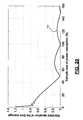
- FIG. 19is a graph of the standard deviation of the time average of the signal power of FIG. 15 versus the sample size of the power calculation.
- FIG. 20is a graph of the standard deviation of the time average of the signal power for a dual frequency RF plasma generation system versus the sample size of the power calculation.
- modulerefers to an Application Specific Integrated Circuit (ASIC), an electronic circuit, a processor (shared, dedicated, or group) and memory that execute one or more software or firmware programs, a combinational logic circuit, and/or other suitable components that provide the described functionality.
- ASICApplication Specific Integrated Circuit
- processorshared, dedicated, or group
- memorythat execute one or more software or firmware programs, a combinational logic circuit, and/or other suitable components that provide the described functionality.
- RF plasma generator system 10includes an RF generator 12 that generates RF power for a plasma chamber 18 .
- An RF sensor 16generates first and second signals that represent respective electrical properties of the RF power.
- RF sensor 16may be implemented with a voltage/current (V/I) sensor or a directional coupler. When RF sensor 16 is implemented with the V/I sensor the first and second signals represent voltage and current of the RF power, respectively. When the RF sensor 16 is implemented with the directional coupler the first and second signals represent forward and reverse power of the RF power, respectively.
- V/Ivoltage/current
- the first and second signalsrepresent forward and reverse power of the RF power, respectively.
- An impedance matching network 14matches an output impedance of RF generator 12 to an input impedance of plasma chamber 18 .
- Impedance matching network 14is shown connected downstream of RF sensor 16 , however it should be appreciated that it may also be connected upstream of RF sensor 16 , i.e. between the RF sensor 16 and plasma chamber 18 .
- An analog to digital (A/D) module 20converts the first and second signals from RF sensor 16 to respective digital signals.
- the digital signalsare communicated to an analysis module 22 .
- Analysis module 22employs a correlation function to detect arcs in plasma chamber 18 based on the first and second signals. The arc detection method is described below in more detail.
- Analysis module 22generates an arc detect signal based on an outcome of the arc detect method.
- the arc detect signalis communicated to a control module 24 and a probabilistic module 36 and indicates whether an arc is occurring in plasma chamber 18 .
- Control module 24generates control signals 26 that control the RF power output of RF generator 12 .
- Control module 24also receives the arc detect signal and the data from the first and second signals via analysis module 22 .
- Control module 24generates an output based on the data and the arc detect signal. The output controls RF generator 12 such that the plasma is generated as desired and any arc detected in the plasma is extinguished in response to the arc detect signal.
- RF generator 12 and/or control module 24generates an enable signal 28 and communicates it to analysis module 22 .
- Enable signal 28is employed when RF generator 12 initiates plasma in plasma chamber 18 . While the plasma is initiating, the voltage and current of the RF power fluctuate. Enable signal 28 holds off or disables analysis module 22 such as to prevent it from misinterpreting the fluctuations as arcs.
- analysis module 22may detect whether the plasma is initiating and obviate a need for enable signal 28 . Analysis module 22 may determine whether plasma is initiating by monitoring the voltage and current of the RF power. When the voltage and current transition from zero to non-zero, then analysis module 22 may hold off generating the arc detect signal until after the voltage and current stabilize at non-zero values.
- a probabilistic module 36may be employed to process the arc detect signal in accordance with a method that is described below.
- Probabilistic module 36uses the arc detect signal to compute a probabilistic model and to predict a probability of an arc event.
- the modelis computed using a Baum-Welch algorithm and the probability of an arc event is computed using a Viterbi algorithm.
- Probabilistic module 36may be an off-line process that generates the model after data is collected.
- the resulting probabilistic modelbecomes a quantitative indicator that determines whether variations to process parameters associated with the semiconductor manufacturing process yield a decreased likelihood of arcs of various durations.
- Analysis module 22includes a subtraction module 30 , a window module 32 , and a correlation module 34 .
- Subtraction module 30subtracts a DC offset from the digital signals that are generated by A/D module 20 .
- Window module 32applies a window function to the digital data from subtraction module 30 .
- Correlation module 34cross correlates the windowed data in accordance with a method that is described below.
- correlation module 34Operation of correlation module 34 will now be described in more detail.
- the wideband, high speed digital data from A/D module 20provides valuable information of the spectral content of the RF power present on the RF transmission line between RF generator 12 and plasma chamber 18 .
- Spatial information contained in these signalsrepresents transitory behavior of systems connected to the RF transmission line.
- Arc detectioncan be achieved by coupling the spatial information with computation of a correlation function within correlation module 34 .
- Probabilistic module 36implements a probabilistic framework to bolster arc detection and provide a quantitative measure to demonstrate process improvement by the reduction of the likelihood of an arc event.
- Arc eventscan be characterized by rapid and abrupt transients that result from a discharge between the RF generated plasma and an electrode of plasma chamber 18 .
- the arc eventsmay damage devices being fabricated during a semiconductor manufacturing process.
- Other arc eventsare characterized by a discharge from the plasma to a sidewall of plasma chamber 18 and/or discharges within the plasma occurring from the build-up of polymer structures within the plasma.
- the polymerization of negative ionsmay also be referred to as dust particles.
- a sheath of the plasma for continuously powered plasmaretains negative ions. After a period of time, these negative ions build up and polymerize to form contaminating particles.
- the transient resulting from the dischargecauses perturbations on the electromagnetic signals represented by the information from A/D module 20 .
- Correlation module 34implements a discrete-time auto correlation function
- nis an index of the digital sample
- ⁇is a lag or delay in the function.
- Two additional properties of Eq. (1)are leveraged for the purpose of arc detection.
- the first propertyis that Eq. (1) contains a measure of the rate of change of the voltage and current.
- the second propertyis the function is periodic if the voltage and current signals contain periodic components.
- the correlationis performed on a windowed version of the digital signal containing N discrete time samples comprising M periods of the fundamental RF signal. Window module 32 applies the windowing function to the digital samples.
- the frequency of the RF poweris referred to as the fundamental signal.
- the fundamental signalis selected as the lowest frequency in the lowest frequency band of operation.
- the procedure to compute a spectral estimation of the signalcommences with subtraction module 30 subtracting a mean ⁇ x from the discrete-time signal x from A/D module 20 .
- x _ ⁇ [ n ]x ⁇ [ n ] - ⁇ x ⁇ ⁇ n ( 3 )
- the autocorrelation function for xis derived from r a [T] and scaled element by element of the autocorrelation function for the window function r w [T].
- FIGS. 3A and 3Bplots of normalized samples acquired at a rate of 100 MSPS are shown.
- FIG. 3Ashows a voltage envelope 50 and
- FIG. 3Bshows current envelope 60 .
- An arc eventoccurs at approximately 150 ⁇ S, which is indicated at arrow 52 and ends approximately 23 ⁇ S later as indicated at arrow 54 .
- the transient behavioris detectable in the voltage and current signals.
- the autocorrelation functionis computed for the voltage and currents signals using a Hanning window of length N.
- the autocorrelation for the voltage signalis shown in FIG. 4 .
- FIG. 5shows the autocorrelation function for the current signal. Since the voltage and current signals contains the periodic component for the fundamental frequency (13.56 MHz in this case, however it should be appreciated that other frequencies may be used) the corresponding correlation functions are also periodic. Lags of ⁇ also indicate periodic harmonic components emitted from the plasma.
- the autocorrelation functionsproduce an abrupt change that coincides with the initial appearance of the arc event.
- FIG. 6shows cross correlation function r ⁇ i [T] ; also produces a periodic function with a visually detectable arc event.
- the arc detection methodshould be invariant to different plasma load impedance and power levels.
- the cross correlation function of the voltage and current signalsprovides immunity to a broader range of signals over an entire Smith Chart.
- the arc eventis apparent between times 52 and 54 (see FIG. 6 ) and detectable from the cross correlation function.
- Nextis a description of how the function can be used for an arc event detector.
- Analysis module 22should keep false positive arc detections to a minimum.
- analysis module 22includes probabilistic module 36 .
- Probabilistic module 36implements a probabilistic framework that assigns likelihood to the number of arc events detected. False positive could be attributed to normally occurring transients and instabilities arising from a change in power levels or even more abrupt, the ignition of the plasma.
- the solution to the latteris employ enable signal 28 to engage arc detection when the plasma is in a steady state. This is important in applications like pulsing, where the plasma state following transition periods could otherwise be mistakenly detected as an arc event.
- Correlation module 34implements a first difference of the correlation function with respect to the j th correlation function, r ⁇ i j ⁇ r ⁇ i j-1 .
- first difference of the autocorrelation functions for the voltage ( FIG. 9 ) and current signals ( FIG. 10 )prominent ridges are detectable for instances in time to detect the commencement and extinguishment of the arc event.
- FIG. 11shows a plot of the normalized output for the cross correlation of the voltage and current. In this plot, the duration of the arc even is palpable with the duration time indicated.
- FIGS. 12A and 12Bshow voltage envelope 50 and FIG. 12B shows current envelope 60 .
- the arcis shown as descending spike at 70 .
- the arc detection using the cross correlation function for voltage and currentis shown at FIG. 13 .
- a first-order Markov chainis shown that describes the probabilistic framework for a procedure to analyze the transitions of an arc event.
- a trellisis created that spans a duration. The duration could equate to the length of time for a process step, the entire process, or greater.
- the Markov chainincludes three states: no arc (S 0 ), arc event detected (S 1 ), and arc event occurring (S 2 ). Probabilities are also presented to describe the transition probabilities P mn from state m to state n. From the two examples used to describe our approach, we can ascertain how this model reflects the detection of varying durations of arcs. In the first example of FIGS. 3A and 3B the arc event lasted approximately 23 uS. For that case, the Markov chain would start at state S 0 and transition to S 1 when the arc event was detected at time 52 . Since that example had an arc event that remained active, the transition from S 1 to S 2 would be indicative of this scenario.
- the eloquence of using this frameworkis it provides the capability to determine the likelihood of an arc event from which the system engineer can use this information to adjust the process parameters and quantitatively determine the resulting improvement.
- the decoding of this sequence, using observations from the arc detector,is accomplished by using the Viterbi algorithm. This algorithm produces the probability of the observed sequence from
- the state transition probabilitiescan also be computed. As adjustments are made and the process is run, the observable information is collected. Using this information with a post-process algorithm, the transition probabilities can be computed and compared to the state transition probabilities prior to the adjustments. These probabilities are computed using an expectation maximization algorithm.
- the expectation maximization algorithmis an iterative algorithm used to maximize the model parameters based on the observed data. There are two steps to the expectation maximization algorithm. In the first step, the probabilities are marginalized given the current model. For the first iteration, initial conditions are applied to the model. During the second iteration the model parameters are optimized. This procedure iterates over these two steps until convergence of the model parameters is achieved. The procedure is described by the pseudo-code of Table 1.
- analysis module 22may be implemented in the analog domain.
- A/D module 20may be eliminated (see FIG. 1 ) and analysis module 22 receives analog first and second signals from RF sensor 16 .
- subtraction module 30 , window module 32 , the window function, and correlation module 34are also implemented in the analog domain.
- Correlation module 34may implement the cross correlation function:
- r vi ⁇ ( ⁇ )⁇ ⁇ n ⁇ v ⁇ [ n ] ⁇ i ⁇ [ n - ⁇ ] , ( 6 )
- ⁇ [n]is the sampled voltage of RF plasma generator system 10 at time n
- i[n]is the sampled current of RF plasma generator system 10 at time n
- ⁇is a lag or delay in the function
- r ⁇ i ( ⁇ )is the cross correlation of voltage and current of RF plasma generator system 10 with a delay of ⁇ .
- the cross correlation functionis a dot product equivalent to the power present in the voltage and current signals.
- the meanis subtracted from each of the voltage and current signals before performing the cross correlation.
- ⁇ [n]is the sampled voltage of RF plasma generator system 10 at time n
- i[n]is the sampled current of RF plasma generator system 10 at time n
- E[ ⁇ [n]]is the mean of ⁇ [n], which may be determined by Eq.
- E[i[n]]is the mean of i[n], which may be determined by Eq. (2) above.
- the determination of the cross-correlation of the voltage and current signals, with no delay, i.e., when ⁇0, provides the power present in the fundamental signal.
- Waveform 100is based on a fundamental signal frequency at 13.56 MHz and a sample rate of 100 MSPS, which corresponds approximately with 7.4 samples per period.
- the beginning of the arc eventis indicated at arrow 52 and arc event ends approximately 23 ⁇ s later, at a time indicated by arrow 54 .
- Arrowed line 105indicates the change in the power of the signal during the arc event, while arrowed line 107 indicates the time duration of the arc event.
- the change in powerwill also be uncalibrated and related to the measured power, and not the actual power, of the signal. If, instead, the change in power determined by the cross correlation function was calibrated to a National Institute of Standards and Technology traceable standard, the result would comprise the change in actual power of the signal. As stated above, the energy lost during the arc event can be estimated by multiplying the change in power by the duration of the arc event.
- waveform 110is a graph of the signal power versus time that illustrates a short duration arc event. Similar to that described above, arrow 52 indicates the beginning of the arc event while arrow 54 indicates the end of the arc event.
- the time duration of the arc eventis indicated by arrows 117 .
- the change in poweris indicated by arrowed line 115 .
- the time duration of the arc eventis limited to one cross correlation block. Thus, the time duration is estimated to be equal to the time duration between such blocks.
- the energy of the arc eventcomprises an estimation rather than an exact value.
- signal power waveforms 100 ′ and 100 ′′comprise alternate signal powers of waveform 100 above in which the number of samples per period is equal to 22 and 32, respectively. Based on these graphs, it is apparent that waveform 100 ′′ is a more variable (or, noisier) version of the waveform 100 and is, therefore, less suitable for estimating the energy of the arc event. For this reason, the number of samples per period (referred to herein as N) plays a role in the accuracy of the measurement system and should not be arbitrarily chosen.
- waveform 100is based on an RF generator 12 frequency of 13.56 MHz and a 100 MSPS sampling rate. Based on these set points, the number of samples is approximately equal to 7.4 per period. Based on the standard deviation waveform 120 , in which the standard deviation reaches its valleys at periodic intervals, the number of samples per period should be selected to be an integer multiple of the number of samples in the period of interest in order to obtain the most suitable signal power estimation. Thus, as illustrated in FIGS.
- waveform 100 ′in which the number of samples per period is equal to 22, is more suitable than waveform 100 ′′, which is related to the number of samples being equal to 32 per period, since the number 22 more closely corresponds with an integer multiple of 7.4 than does the number 32.
- FIG. 20a graph of the standard deviation 130 of the time average of the power of a dual frequency RF generator system versus the sample size of the power calculation is illustrated.
- the dual frequenciesare 2 MHz and 27.12 MHz in this example.
- the standard deviation 130reaches its valleys at multiples of the number of samples in the period of interest corresponding to 2 MHz, i.e., at multiples of 50.
- the number of samples per periodshould be chosen based on the lowest frequency of the RF generator.
Landscapes
- Physics & Mathematics (AREA)
- General Physics & Mathematics (AREA)
- Engineering & Computer Science (AREA)
- Plasma & Fusion (AREA)
- Chemical & Material Sciences (AREA)
- Analytical Chemistry (AREA)
- Spectroscopy & Molecular Physics (AREA)
- Plasma Technology (AREA)
- Chemical Vapour Deposition (AREA)
- Drying Of Semiconductors (AREA)
- Testing Relating To Insulation (AREA)
Abstract
Description
wherein ν[n] is the voltage at time n; i[n] is the current at time n; rνi(τ:=0) is the power estimate at time n; E[ν[n]] is a mean of ν[n] at time n; E[i[n]] is a mean of i[n] at time n; and ∀n comprises all times n in a window of interest.
wherein ν[n] is the voltage at time n; i[n] is the current at time n; rνi(τ:=0) is the power estimate at time n; E[ν[n]] is a mean of ν[n] at time n; E[i[n]] is a mean of i[n] at time n; and ∀n comprises all times n in a window of interest.
a[n]=w[n](x[n]−μx)∀n (4)
where w represents the vector of unobservable states in our model It should be appreciated that no limitation is placed on including other observable information such as RF and other process affecting parameters.
| TABLE 1 | |||
| 1.) | Initialize model parameters and obtain | ||
| 2.) | Until Convergence | ||
| a. | Compute the estimated transition | ||
| probabilities α(j) | |||
| b. | Compute the estimated state probabilities | ||
| β(j) | |||
| c. | Update α(j+1) := α(j) | ||
| d. | Update β (j+1) := β (j) | ||
| 3.) | End | ||
where ν[n] is the sampled voltage of RF
where ν[n] is the sampled voltage of RF
Energy=ΔP·t, (8)
where ΔP is the difference between the cross correlation (with no delay) of the voltage and current signals preceding the arc event with that during the arc event, e.g., determined by the equation above; and t is the time duration of the arc event. Based on this equation, the system engineer may estimate the change in energy delivered to the
Claims (24)
Priority Applications (11)
| Application Number | Priority Date | Filing Date | Title |
|---|---|---|---|
| US12/175,867US8289029B2 (en) | 2008-02-14 | 2008-07-18 | Application of wideband sampling for arc detection with a probabilistic model for quantitatively measuring arc events |
| PCT/US2008/083347WO2009102358A1 (en) | 2008-02-14 | 2008-11-13 | Application of wideband sampling for arc detection with a probabilistic model for quantitatively measuring arc events |
| JP2010546746AJP5583603B2 (en) | 2008-02-14 | 2008-11-13 | Arc detection system and method |
| GB1009777.2AGB2468430B (en) | 2008-02-14 | 2008-11-13 | Application of wideband sampling for arc detection with a probabilistic model for quantitatively measuring arc events |
| DE112008003705.1TDE112008003705B4 (en) | 2008-02-14 | 2008-11-13 | Applying broadband scanning to arc detection with a probabilistic model to quantitatively measure arc events |
| KR1020107013838AKR101430165B1 (en) | 2008-02-14 | 2008-11-13 | Application of wideband sampling for arc detection with a probabilistic model for quantitatively measuring arc events |
| GB1219888.3AGB2493122B (en) | 2008-02-14 | 2008-11-13 | Application of wideband sampling for arc detection with a probabilistic model for quantitatively measuring arc events |
| CN2008801144154ACN101843178B (en) | 2008-02-14 | 2008-11-13 | Broadband Sampling Applications for Arc Detection Using Probabilistic Models for Quantitative Measurement of Arc Events |
| TW097146458ATWI496513B (en) | 2008-02-14 | 2008-11-28 | Arc detecting device for plasma generating system and detecting method thereof |
| US12/727,715US8334700B2 (en) | 2008-02-14 | 2010-03-19 | Arc detection |
| US13/648,317US8581597B2 (en) | 2008-02-14 | 2012-10-10 | Application of wideband sampling for arc detection with a probabilistic model for quantitatively measuring arc events |
Applications Claiming Priority (2)
| Application Number | Priority Date | Filing Date | Title |
|---|---|---|---|
| US12/031,171US8264237B2 (en) | 2008-02-14 | 2008-02-14 | Application of wideband sampling for arc detection with a probabilistic model for quantitatively measuring arc events |
| US12/175,867US8289029B2 (en) | 2008-02-14 | 2008-07-18 | Application of wideband sampling for arc detection with a probabilistic model for quantitatively measuring arc events |
Related Parent Applications (1)
| Application Number | Title | Priority Date | Filing Date |
|---|---|---|---|
| US12/031,171Continuation-In-PartUS8264237B2 (en) | 2008-02-14 | 2008-02-14 | Application of wideband sampling for arc detection with a probabilistic model for quantitatively measuring arc events |
Related Child Applications (2)
| Application Number | Title | Priority Date | Filing Date |
|---|---|---|---|
| US12/727,715Continuation-In-PartUS8334700B2 (en) | 2008-02-14 | 2010-03-19 | Arc detection |
| US13/648,317ContinuationUS8581597B2 (en) | 2008-02-14 | 2012-10-10 | Application of wideband sampling for arc detection with a probabilistic model for quantitatively measuring arc events |
Publications (2)
| Publication Number | Publication Date |
|---|---|
| US20090207537A1 US20090207537A1 (en) | 2009-08-20 |
| US8289029B2true US8289029B2 (en) | 2012-10-16 |
Family
ID=40954897
Family Applications (2)
| Application Number | Title | Priority Date | Filing Date |
|---|---|---|---|
| US12/175,867Active2028-09-06US8289029B2 (en) | 2008-02-14 | 2008-07-18 | Application of wideband sampling for arc detection with a probabilistic model for quantitatively measuring arc events |
| US13/648,317ActiveUS8581597B2 (en) | 2008-02-14 | 2012-10-10 | Application of wideband sampling for arc detection with a probabilistic model for quantitatively measuring arc events |
Family Applications After (1)
| Application Number | Title | Priority Date | Filing Date |
|---|---|---|---|
| US13/648,317ActiveUS8581597B2 (en) | 2008-02-14 | 2012-10-10 | Application of wideband sampling for arc detection with a probabilistic model for quantitatively measuring arc events |
Country Status (8)
| Country | Link |
|---|---|
| US (2) | US8289029B2 (en) |
| JP (1) | JP5583603B2 (en) |
| KR (1) | KR101430165B1 (en) |
| CN (1) | CN101843178B (en) |
| DE (1) | DE112008003705B4 (en) |
| GB (2) | GB2468430B (en) |
| TW (1) | TWI496513B (en) |
| WO (1) | WO2009102358A1 (en) |
Cited By (40)
| Publication number | Priority date | Publication date | Assignee | Title |
|---|---|---|---|---|
| US20110057662A1 (en)* | 2008-04-21 | 2011-03-10 | Thomas Eriksson | Arc Detector And Associated Method For Detecting Undesired Arcs |
| US20130073241A1 (en)* | 2008-02-14 | 2013-03-21 | Mks Instruments, Inc. | Application Of Wideband Sampling For Arc Detection With A Probabilistic Model For Quantitatively Measuring Arc Events |
| US9196459B2 (en) | 2014-01-10 | 2015-11-24 | Reno Technologies, Inc. | RF impedance matching network |
| US9306533B1 (en) | 2015-02-20 | 2016-04-05 | Reno Technologies, Inc. | RF impedance matching network |
| US9496122B1 (en) | 2014-01-10 | 2016-11-15 | Reno Technologies, Inc. | Electronically variable capacitor and RF matching network incorporating same |
| US9525412B2 (en) | 2015-02-18 | 2016-12-20 | Reno Technologies, Inc. | Switching circuit |
| US9697991B2 (en) | 2014-01-10 | 2017-07-04 | Reno Technologies, Inc. | RF impedance matching network |
| US9729122B2 (en) | 2015-02-18 | 2017-08-08 | Reno Technologies, Inc. | Switching circuit |
| US9755641B1 (en) | 2014-01-10 | 2017-09-05 | Reno Technologies, Inc. | High speed high voltage switching circuit |
| US9844127B2 (en) | 2014-01-10 | 2017-12-12 | Reno Technologies, Inc. | High voltage switching circuit |
| US9865432B1 (en) | 2014-01-10 | 2018-01-09 | Reno Technologies, Inc. | RF impedance matching network |
| US10340879B2 (en) | 2015-02-18 | 2019-07-02 | Reno Technologies, Inc. | Switching circuit |
| US10431428B2 (en) | 2014-01-10 | 2019-10-01 | Reno Technologies, Inc. | System for providing variable capacitance |
| US10455729B2 (en) | 2014-01-10 | 2019-10-22 | Reno Technologies, Inc. | Enclosure cooling system |
| US10483090B2 (en) | 2017-07-10 | 2019-11-19 | Reno Technologies, Inc. | Restricted capacitor switching |
| US10692699B2 (en) | 2015-06-29 | 2020-06-23 | Reno Technologies, Inc. | Impedance matching with restricted capacitor switching |
| US10714314B1 (en) | 2017-07-10 | 2020-07-14 | Reno Technologies, Inc. | Impedance matching network and method |
| US10727029B2 (en) | 2017-07-10 | 2020-07-28 | Reno Technologies, Inc | Impedance matching using independent capacitance and frequency control |
| US10984986B2 (en) | 2015-06-29 | 2021-04-20 | Reno Technologies, Inc. | Impedance matching network and method |
| US11081316B2 (en) | 2015-06-29 | 2021-08-03 | Reno Technologies, Inc. | Impedance matching network and method |
| US11101110B2 (en) | 2017-07-10 | 2021-08-24 | Reno Technologies, Inc. | Impedance matching network and method |
| US11114280B2 (en) | 2017-07-10 | 2021-09-07 | Reno Technologies, Inc. | Impedance matching with multi-level power setpoint |
| US11150283B2 (en) | 2015-06-29 | 2021-10-19 | Reno Technologies, Inc. | Amplitude and phase detection circuit |
| US11269001B2 (en)* | 2018-09-11 | 2022-03-08 | HKC Corporation Limited | Monitoring device for monitoring an arc discharge in a dry etching machine configured to dry-etch a display panel, electrostatic chuck of the dry-etching machine, and monitoring method of the monitoring device |
| US11289307B2 (en) | 2017-07-10 | 2022-03-29 | Reno Technologies, Inc. | Impedance matching network and method |
| US11315758B2 (en) | 2017-07-10 | 2022-04-26 | Reno Technologies, Inc. | Impedance matching using electronically variable capacitance and frequency considerations |
| US11335540B2 (en) | 2015-06-29 | 2022-05-17 | Reno Technologies, Inc. | Impedance matching network and method |
| US11342161B2 (en) | 2015-06-29 | 2022-05-24 | Reno Technologies, Inc. | Switching circuit with voltage bias |
| US11342160B2 (en) | 2015-06-29 | 2022-05-24 | Reno Technologies, Inc. | Filter for impedance matching |
| US11393659B2 (en) | 2017-07-10 | 2022-07-19 | Reno Technologies, Inc. | Impedance matching network and method |
| US11398370B2 (en) | 2017-07-10 | 2022-07-26 | Reno Technologies, Inc. | Semiconductor manufacturing using artificial intelligence |
| US11476091B2 (en) | 2017-07-10 | 2022-10-18 | Reno Technologies, Inc. | Impedance matching network for diagnosing plasma chamber |
| US11521831B2 (en) | 2019-05-21 | 2022-12-06 | Reno Technologies, Inc. | Impedance matching network and method with reduced memory requirements |
| US11521833B2 (en) | 2017-07-10 | 2022-12-06 | Reno Technologies, Inc. | Combined RF generator and RF solid-state matching network |
| US11536755B2 (en) | 2020-05-29 | 2022-12-27 | Mks Instruments, Inc. | System and method for arc detection using a bias RF generator signal |
| US11631570B2 (en) | 2015-02-18 | 2023-04-18 | Reno Technologies, Inc. | Switching circuit |
| US12119206B2 (en) | 2015-02-18 | 2024-10-15 | Asm America, Inc. | Switching circuit |
| US12272522B2 (en) | 2017-07-10 | 2025-04-08 | Asm America, Inc. | Resonant filter for solid state RF impedance matching network |
| US12334307B2 (en) | 2017-07-10 | 2025-06-17 | Asm Ip Holding B.V. | Power control for rf impedance matching network |
| US12444573B2 (en) | 2022-04-18 | 2025-10-14 | Asm America, Inc. | Impedance matching network and method |
Families Citing this family (20)
| Publication number | Priority date | Publication date | Assignee | Title |
|---|---|---|---|---|
| DE102011077152B4 (en) | 2011-06-07 | 2015-08-13 | TRUMPF Hüttinger GmbH + Co. KG | Method for generating an arc detection signal and Arcerkennungsungsanordnung |
| KR101843443B1 (en)* | 2011-10-19 | 2018-05-15 | 삼성전자주식회사 | plasma equipment and maintenance method of the same |
| KR101303040B1 (en)* | 2012-02-28 | 2013-09-03 | 주식회사 뉴파워 프라즈마 | Method and apparatus for detecting arc in plasma chamber |
| US9043525B2 (en) | 2012-12-14 | 2015-05-26 | Lam Research Corporation | Optimizing a rate of transfer of data between an RF generator and a host system within a plasma tool |
| US10049857B2 (en)* | 2014-12-04 | 2018-08-14 | Mks Instruments, Inc. | Adaptive periodic waveform controller |
| EP3035365A1 (en)* | 2014-12-19 | 2016-06-22 | TRUMPF Huettinger Sp. Z o. o. | Method of detecting an arc occurring during the power supply of a plasma process, control unit for a plasma power supply, and plasma power supply |
| CN104882884A (en)* | 2015-02-27 | 2015-09-02 | 国网河南省电力公司电力科学研究院 | System harmonic probability evaluating method based on Markov chain Monte Carlo method |
| JP6814213B2 (en)* | 2015-12-04 | 2021-01-13 | アプライド マテリアルズ インコーポレイテッドApplied Materials,Incorporated | Eakring detector for plasma processing |
| US10879044B2 (en)* | 2017-04-07 | 2020-12-29 | Lam Research Corporation | Auxiliary circuit in RF matching network for frequency tuning assisted dual-level pulsing |
| US10170287B1 (en) | 2017-10-16 | 2019-01-01 | Taiwan Semiconductor Manufacturing Co., Ltd. | Techniques for detecting micro-arcing occurring inside a semiconductor processing chamber |
| DE102018116637A1 (en) | 2018-07-10 | 2020-01-16 | TRUMPF Hüttinger GmbH + Co. KG | Power supply facility and operating procedures therefor |
| US12230475B2 (en)* | 2018-08-14 | 2025-02-18 | Tokyo Electron Limited | Systems and methods of control for plasma processing |
| KR20230027035A (en)* | 2020-05-27 | 2023-02-27 | 램 리써치 코포레이션 | Sensor data compression in plasma tools |
| JP7417963B2 (en)* | 2020-08-26 | 2024-01-19 | パナソニックIpマネジメント株式会社 | Arc detection device, arc detection system, arc detection method, and program |
| TWI755139B (en)* | 2020-11-03 | 2022-02-11 | 台達電子工業股份有限公司 | Signal sampling circuit for arc detection |
| CN114446752B (en)* | 2020-11-04 | 2024-04-05 | 中微半导体设备(上海)股份有限公司 | Method and device for detecting electric arc in plasma processing cavity |
| KR102208819B1 (en)* | 2020-12-09 | 2021-01-28 | 주식회사 더블유지에스 | Rf signal monitoring apparatus and system for monioring an arc event generated in a plasma process |
| KR102673673B1 (en) | 2021-12-09 | 2024-06-07 | 한국핵융합에너지연구원 | Plasma status detecting apparatus using rf signal, and plasma status detecting method using the same |
| WO2023239541A1 (en)* | 2022-06-08 | 2023-12-14 | Lam Research Corporation | Systems and methods for compressing a sensor-based signal |
| CN117828275B (en)* | 2024-01-10 | 2024-07-02 | 江苏神州半导体科技有限公司 | Prediction method and device for plasma chamber arcing |
Citations (25)
| Publication number | Priority date | Publication date | Assignee | Title |
|---|---|---|---|---|
| US3020529A (en) | 1959-12-21 | 1962-02-06 | Collins Radio Co | Reflected power alarm for a variable power output antenna system |
| US3519927A (en) | 1968-09-05 | 1970-07-07 | Us Air Force | Scanning analyzer for determining characteristics of an ionized plasma |
| US4588952A (en) | 1982-12-16 | 1986-05-13 | Japan Atomic Energy Research Institute | Arc discharge abnormality detecting system |
| JPH0831806A (en) | 1994-07-20 | 1996-02-02 | Hitachi Ltd | Plasma processing device |
| JPH08277468A (en) | 1995-04-04 | 1996-10-22 | Ulvac Japan Ltd | Dc power source of vacuum device |
| US5810963A (en) | 1995-09-28 | 1998-09-22 | Kabushiki Kaisha Toshiba | Plasma processing apparatus and method |
| US6124758A (en) | 1998-08-19 | 2000-09-26 | Harris Corporation | RF power amplifier control system |
| US20030046013A1 (en)* | 1998-02-27 | 2003-03-06 | Gerrish Kevin S. | Voltage current sensor with high matching directivity |
| US20030063420A1 (en) | 2001-09-28 | 2003-04-03 | Eaton Corporation | Method and apparatus for detecting and suppressing a parallel ARC fault |
| US20030205460A1 (en)* | 2002-04-12 | 2003-11-06 | Buda Paul R. | Apparatus and method for arc detection |
| US6718272B1 (en) | 2000-11-01 | 2004-04-06 | Eni Technology Inc. | Fast transient protection for RF plasma generator |
| US20050040144A1 (en) | 2003-08-18 | 2005-02-24 | Eni Technology, Inc. | Control of plasma transitions in sputter processing systems |
| US6902646B2 (en) | 2003-08-14 | 2005-06-07 | Advanced Energy Industries, Inc. | Sensor array for measuring plasma characteristics in plasma processing environments |
| US6954077B2 (en) | 2002-01-31 | 2005-10-11 | Tokyo Electron Limited | Apparatus and method for improving microwave coupling to a resonant cavity |
| US20060025820A1 (en)* | 2004-07-27 | 2006-02-02 | The Cleveland Clinic Foundation | Integrated system and method for MRI-safe implantable devices |
| US20060049831A1 (en)* | 2004-09-04 | 2006-03-09 | Applied Materials, Inc. | Detection and suppression of electrical arcing |
| US20060252283A1 (en) | 2003-08-07 | 2006-11-09 | Hitachi Kokusai Electric Inc. | Substrate processing apparatus and sustrate processing method |
| US20060259259A1 (en) | 2005-05-02 | 2006-11-16 | Mks Instruments, Inc. | Versatile semiconductor manufacturing controller with statistically repeatable response times |
| US7199327B2 (en) | 2002-06-28 | 2007-04-03 | Tokyo Electron Limited | Method and system for arc suppression in a plasma processing system |
| JP2007149596A (en) | 2005-11-30 | 2007-06-14 | Daihen Corp | Arc detector of plasma treatment system |
| US7301286B2 (en) | 2001-10-22 | 2007-11-27 | Shibaura Mechatronics Corporation | Method of detecting an arc in a glow-discharge device and apparatus for controlling a high-frequency arc discharge |
| US7305311B2 (en) | 2005-04-22 | 2007-12-04 | Advanced Energy Industries, Inc. | Arc detection and handling in radio frequency power applications |
| US20080021664A1 (en) | 2002-04-12 | 2008-01-24 | Schneider Automation Inc. | Current-Based Method and Apparatus for Detecting and Classifying Arcs |
| US20080197854A1 (en) | 2007-02-16 | 2008-08-21 | Mks Instruments, Inc. | Harmonic Derived Arc Detector |
| US7570028B2 (en) | 2007-04-26 | 2009-08-04 | Advanced Energy Industries, Inc. | Method and apparatus for modifying interactions between an electrical generator and a nonlinear load |
Family Cites Families (13)
| Publication number | Priority date | Publication date | Assignee | Title |
|---|---|---|---|---|
| US5175472A (en) | 1991-12-30 | 1992-12-29 | Comdel, Inc. | Power monitor of RF plasma |
| US5892198A (en) | 1996-03-29 | 1999-04-06 | Lam Research Corporation | Method of and apparatus for electronically controlling r.f. energy supplied to a vacuum plasma processor and memory for same |
| US6332961B1 (en) | 1997-09-17 | 2001-12-25 | Tokyo Electron Limited | Device and method for detecting and preventing arcing in RF plasma systems |
| JPH11260807A (en)* | 1997-12-17 | 1999-09-24 | Toshiba Corp | Plasma processing end point detection method and apparatus or abnormal discharge detection method and apparatus, and semiconductor manufacturing method |
| JP2001135579A (en)* | 1999-11-02 | 2001-05-18 | Hitachi Kokusai Electric Inc | Plasma processing equipment |
| JP3893276B2 (en)* | 2001-12-04 | 2007-03-14 | 株式会社日立ハイテクノロジーズ | Plasma processing equipment |
| US7345428B2 (en) | 2002-09-23 | 2008-03-18 | Turner Terry R | Transducer package for process control |
| US7728250B2 (en) | 2004-02-02 | 2010-06-01 | Inficon, Inc. | RF sensor clamp assembly |
| US6943317B1 (en)* | 2004-07-02 | 2005-09-13 | Advanced Energy Industries, Inc. | Apparatus and method for fast arc extinction with early shunting of arc current in plasma |
| JP2006288009A (en)* | 2005-03-31 | 2006-10-19 | Daihen Corp | High-frequency power supply unit |
| JP4837369B2 (en)* | 2005-11-30 | 2011-12-14 | 株式会社ダイヘン | Arc detector for plasma processing system |
| ES2321309T3 (en)* | 2005-12-22 | 2009-06-04 | Huttinger Elektronik Gmbh + Co. Kg | PROCEDURE AND DEVICE FOR DETECTION OF AN ARC. |
| US8289029B2 (en)* | 2008-02-14 | 2012-10-16 | Mks Instruments, Inc. | Application of wideband sampling for arc detection with a probabilistic model for quantitatively measuring arc events |
- 2008
- 2008-07-18USUS12/175,867patent/US8289029B2/enactiveActive
- 2008-11-13WOPCT/US2008/083347patent/WO2009102358A1/enactiveApplication Filing
- 2008-11-13CNCN2008801144154Apatent/CN101843178B/enactiveActive
- 2008-11-13GBGB1009777.2Apatent/GB2468430B/ennot_activeExpired - Fee Related
- 2008-11-13JPJP2010546746Apatent/JP5583603B2/ennot_activeExpired - Fee Related
- 2008-11-13GBGB1219888.3Apatent/GB2493122B/ennot_activeExpired - Fee Related
- 2008-11-13KRKR1020107013838Apatent/KR101430165B1/ennot_activeExpired - Fee Related
- 2008-11-13DEDE112008003705.1Tpatent/DE112008003705B4/ennot_activeExpired - Fee Related
- 2008-11-28TWTW097146458Apatent/TWI496513B/ennot_activeIP Right Cessation
- 2012
- 2012-10-10USUS13/648,317patent/US8581597B2/enactiveActive
Patent Citations (30)
| Publication number | Priority date | Publication date | Assignee | Title |
|---|---|---|---|---|
| US3020529A (en) | 1959-12-21 | 1962-02-06 | Collins Radio Co | Reflected power alarm for a variable power output antenna system |
| US3519927A (en) | 1968-09-05 | 1970-07-07 | Us Air Force | Scanning analyzer for determining characteristics of an ionized plasma |
| US4588952A (en) | 1982-12-16 | 1986-05-13 | Japan Atomic Energy Research Institute | Arc discharge abnormality detecting system |
| JPH0831806A (en) | 1994-07-20 | 1996-02-02 | Hitachi Ltd | Plasma processing device |
| JPH08277468A (en) | 1995-04-04 | 1996-10-22 | Ulvac Japan Ltd | Dc power source of vacuum device |
| US5810963A (en) | 1995-09-28 | 1998-09-22 | Kabushiki Kaisha Toshiba | Plasma processing apparatus and method |
| US20030046013A1 (en)* | 1998-02-27 | 2003-03-06 | Gerrish Kevin S. | Voltage current sensor with high matching directivity |
| US6124758A (en) | 1998-08-19 | 2000-09-26 | Harris Corporation | RF power amplifier control system |
| US6718272B1 (en) | 2000-11-01 | 2004-04-06 | Eni Technology Inc. | Fast transient protection for RF plasma generator |
| US20030063420A1 (en) | 2001-09-28 | 2003-04-03 | Eaton Corporation | Method and apparatus for detecting and suppressing a parallel ARC fault |
| US7301286B2 (en) | 2001-10-22 | 2007-11-27 | Shibaura Mechatronics Corporation | Method of detecting an arc in a glow-discharge device and apparatus for controlling a high-frequency arc discharge |
| US6954077B2 (en) | 2002-01-31 | 2005-10-11 | Tokyo Electron Limited | Apparatus and method for improving microwave coupling to a resonant cavity |
| US20030205460A1 (en)* | 2002-04-12 | 2003-11-06 | Buda Paul R. | Apparatus and method for arc detection |
| US20040182697A1 (en) | 2002-04-12 | 2004-09-23 | Buda Paul R. | ARC detection approach |
| US20080021664A1 (en) | 2002-04-12 | 2008-01-24 | Schneider Automation Inc. | Current-Based Method and Apparatus for Detecting and Classifying Arcs |
| US7199327B2 (en) | 2002-06-28 | 2007-04-03 | Tokyo Electron Limited | Method and system for arc suppression in a plasma processing system |
| US20060252283A1 (en) | 2003-08-07 | 2006-11-09 | Hitachi Kokusai Electric Inc. | Substrate processing apparatus and sustrate processing method |
| US7767053B2 (en) | 2003-08-07 | 2010-08-03 | Hitachi Kokusai Electric Inc. | Substrate processing apparatus and substrate processing method |
| US6902646B2 (en) | 2003-08-14 | 2005-06-07 | Advanced Energy Industries, Inc. | Sensor array for measuring plasma characteristics in plasma processing environments |
| US20050040144A1 (en) | 2003-08-18 | 2005-02-24 | Eni Technology, Inc. | Control of plasma transitions in sputter processing systems |
| US20060025820A1 (en)* | 2004-07-27 | 2006-02-02 | The Cleveland Clinic Foundation | Integrated system and method for MRI-safe implantable devices |
| US20060049831A1 (en)* | 2004-09-04 | 2006-03-09 | Applied Materials, Inc. | Detection and suppression of electrical arcing |
| US7292045B2 (en) | 2004-09-04 | 2007-11-06 | Applied Materials, Inc. | Detection and suppression of electrical arcing |
| US7514936B2 (en) | 2004-09-04 | 2009-04-07 | Applied Materials, Inc. | Detection and suppression of electrical arcing |
| US7305311B2 (en) | 2005-04-22 | 2007-12-04 | Advanced Energy Industries, Inc. | Arc detection and handling in radio frequency power applications |
| US20060259259A1 (en) | 2005-05-02 | 2006-11-16 | Mks Instruments, Inc. | Versatile semiconductor manufacturing controller with statistically repeatable response times |
| JP2007149596A (en) | 2005-11-30 | 2007-06-14 | Daihen Corp | Arc detector of plasma treatment system |
| US20080197854A1 (en) | 2007-02-16 | 2008-08-21 | Mks Instruments, Inc. | Harmonic Derived Arc Detector |
| US7728602B2 (en)* | 2007-02-16 | 2010-06-01 | Mks Instruments, Inc. | Harmonic derived arc detector |
| US7570028B2 (en) | 2007-04-26 | 2009-08-04 | Advanced Energy Industries, Inc. | Method and apparatus for modifying interactions between an electrical generator and a nonlinear load |
Non-Patent Citations (2)
| Title |
|---|
| British Examination Report for GB1009777.2 dated Jul. 19, 2012. |
| International Search Report for International Patent Application No. PCT/US2008/083347 dated Jul. 2, 2009. |
Cited By (56)
| Publication number | Priority date | Publication date | Assignee | Title |
|---|---|---|---|---|
| US20130073241A1 (en)* | 2008-02-14 | 2013-03-21 | Mks Instruments, Inc. | Application Of Wideband Sampling For Arc Detection With A Probabilistic Model For Quantitatively Measuring Arc Events |
| US8581597B2 (en)* | 2008-02-14 | 2013-11-12 | Msk Instruments, Inc. | Application of wideband sampling for arc detection with a probabilistic model for quantitatively measuring arc events |
| US20110057662A1 (en)* | 2008-04-21 | 2011-03-10 | Thomas Eriksson | Arc Detector And Associated Method For Detecting Undesired Arcs |
| US8508233B2 (en)* | 2008-04-21 | 2013-08-13 | Abb Research Ltd. | Arc detector and associated method for detecting undesired arcs |
| US10026594B2 (en) | 2014-01-10 | 2018-07-17 | Reno Technologies, Inc. | RF impedance matching network |
| US10431428B2 (en) | 2014-01-10 | 2019-10-01 | Reno Technologies, Inc. | System for providing variable capacitance |
| US9697991B2 (en) | 2014-01-10 | 2017-07-04 | Reno Technologies, Inc. | RF impedance matching network |
| US11189466B2 (en) | 2014-01-10 | 2021-11-30 | Reno Technologies, Inc. | High voltage switching circuit |
| US11195698B2 (en) | 2014-01-10 | 2021-12-07 | Reno Technologies, Inc. | RF impedance matching circuit and systems and methods incorporating same |
| US9755641B1 (en) | 2014-01-10 | 2017-09-05 | Reno Technologies, Inc. | High speed high voltage switching circuit |
| US9844127B2 (en) | 2014-01-10 | 2017-12-12 | Reno Technologies, Inc. | High voltage switching circuit |
| US9865432B1 (en) | 2014-01-10 | 2018-01-09 | Reno Technologies, Inc. | RF impedance matching network |
| US9196459B2 (en) | 2014-01-10 | 2015-11-24 | Reno Technologies, Inc. | RF impedance matching network |
| US10707057B2 (en) | 2014-01-10 | 2020-07-07 | Reno Technologies, Inc. | RF impedance matching circuit and systems and methods incorporating same |
| US12334306B2 (en) | 2014-01-10 | 2025-06-17 | Asm America, Inc. | RF impedance matching network |
| US9496122B1 (en) | 2014-01-10 | 2016-11-15 | Reno Technologies, Inc. | Electronically variable capacitor and RF matching network incorporating same |
| US10455729B2 (en) | 2014-01-10 | 2019-10-22 | Reno Technologies, Inc. | Enclosure cooling system |
| US10460912B2 (en) | 2014-01-10 | 2019-10-29 | Reno Technologies, Inc. | RF impedance matching circuit and systems and methods incorporating same |
| US10340879B2 (en) | 2015-02-18 | 2019-07-02 | Reno Technologies, Inc. | Switching circuit |
| US12119206B2 (en) | 2015-02-18 | 2024-10-15 | Asm America, Inc. | Switching circuit |
| US10217608B2 (en) | 2015-02-18 | 2019-02-26 | Reno Technologies, Inc. | Switching circuit for RF currents |
| US11631570B2 (en) | 2015-02-18 | 2023-04-18 | Reno Technologies, Inc. | Switching circuit |
| US9729122B2 (en) | 2015-02-18 | 2017-08-08 | Reno Technologies, Inc. | Switching circuit |
| US9525412B2 (en) | 2015-02-18 | 2016-12-20 | Reno Technologies, Inc. | Switching circuit |
| US9306533B1 (en) | 2015-02-20 | 2016-04-05 | Reno Technologies, Inc. | RF impedance matching network |
| US9584090B2 (en) | 2015-02-20 | 2017-02-28 | Reno Technologies, Inc. | RF impedance matching network |
| US11081316B2 (en) | 2015-06-29 | 2021-08-03 | Reno Technologies, Inc. | Impedance matching network and method |
| US11335540B2 (en) | 2015-06-29 | 2022-05-17 | Reno Technologies, Inc. | Impedance matching network and method |
| US10692699B2 (en) | 2015-06-29 | 2020-06-23 | Reno Technologies, Inc. | Impedance matching with restricted capacitor switching |
| US10984986B2 (en) | 2015-06-29 | 2021-04-20 | Reno Technologies, Inc. | Impedance matching network and method |
| US11342160B2 (en) | 2015-06-29 | 2022-05-24 | Reno Technologies, Inc. | Filter for impedance matching |
| US11150283B2 (en) | 2015-06-29 | 2021-10-19 | Reno Technologies, Inc. | Amplitude and phase detection circuit |
| US11342161B2 (en) | 2015-06-29 | 2022-05-24 | Reno Technologies, Inc. | Switching circuit with voltage bias |
| US11393659B2 (en) | 2017-07-10 | 2022-07-19 | Reno Technologies, Inc. | Impedance matching network and method |
| US10714314B1 (en) | 2017-07-10 | 2020-07-14 | Reno Technologies, Inc. | Impedance matching network and method |
| US10483090B2 (en) | 2017-07-10 | 2019-11-19 | Reno Technologies, Inc. | Restricted capacitor switching |
| US11289307B2 (en) | 2017-07-10 | 2022-03-29 | Reno Technologies, Inc. | Impedance matching network and method |
| US11315758B2 (en) | 2017-07-10 | 2022-04-26 | Reno Technologies, Inc. | Impedance matching using electronically variable capacitance and frequency considerations |
| US10720309B1 (en) | 2017-07-10 | 2020-07-21 | Reno Technologies, Inc. | Impedance matching network and method |
| US10727029B2 (en) | 2017-07-10 | 2020-07-28 | Reno Technologies, Inc | Impedance matching using independent capacitance and frequency control |
| US11114280B2 (en) | 2017-07-10 | 2021-09-07 | Reno Technologies, Inc. | Impedance matching with multi-level power setpoint |
| US11101110B2 (en) | 2017-07-10 | 2021-08-24 | Reno Technologies, Inc. | Impedance matching network and method |
| US11398370B2 (en) | 2017-07-10 | 2022-07-26 | Reno Technologies, Inc. | Semiconductor manufacturing using artificial intelligence |
| US11476091B2 (en) | 2017-07-10 | 2022-10-18 | Reno Technologies, Inc. | Impedance matching network for diagnosing plasma chamber |
| US12334307B2 (en) | 2017-07-10 | 2025-06-17 | Asm Ip Holding B.V. | Power control for rf impedance matching network |
| US11521833B2 (en) | 2017-07-10 | 2022-12-06 | Reno Technologies, Inc. | Combined RF generator and RF solid-state matching network |
| US12272522B2 (en) | 2017-07-10 | 2025-04-08 | Asm America, Inc. | Resonant filter for solid state RF impedance matching network |
| US10741364B1 (en) | 2017-07-10 | 2020-08-11 | Reno Technologies, Inc. | Impedance matching network and method |
| US11557461B2 (en) | 2017-07-10 | 2023-01-17 | Reno Technologies, Inc. | Impedance matching network |
| US11264210B2 (en) | 2017-07-10 | 2022-03-01 | Reno Technologies, Inc. | Impedance matching network and method |
| US11948775B2 (en) | 2017-07-10 | 2024-04-02 | Asm America, Inc. | Combined RF generator and RF solid-state matching network |
| US11269001B2 (en)* | 2018-09-11 | 2022-03-08 | HKC Corporation Limited | Monitoring device for monitoring an arc discharge in a dry etching machine configured to dry-etch a display panel, electrostatic chuck of the dry-etching machine, and monitoring method of the monitoring device |
| US11538662B2 (en) | 2019-05-21 | 2022-12-27 | Reno Technologies, Inc. | Impedance matching network and method with reduced memory requirements |
| US11521831B2 (en) | 2019-05-21 | 2022-12-06 | Reno Technologies, Inc. | Impedance matching network and method with reduced memory requirements |
| US11536755B2 (en) | 2020-05-29 | 2022-12-27 | Mks Instruments, Inc. | System and method for arc detection using a bias RF generator signal |
| US12444573B2 (en) | 2022-04-18 | 2025-10-14 | Asm America, Inc. | Impedance matching network and method |
Also Published As
| Publication number | Publication date |
|---|---|
| TWI496513B (en) | 2015-08-11 |
| WO2009102358A1 (en) | 2009-08-20 |
| DE112008003705B4 (en) | 2023-11-16 |
| CN101843178A (en) | 2010-09-22 |
| KR101430165B1 (en) | 2014-08-18 |
| GB2493122B (en) | 2013-03-20 |
| GB201219888D0 (en) | 2012-12-19 |
| GB201009777D0 (en) | 2010-07-21 |
| GB2468430B (en) | 2012-12-26 |
| DE112008003705T5 (en) | 2010-12-30 |
| TW200935988A (en) | 2009-08-16 |
| JP2011524601A (en) | 2011-09-01 |
| GB2468430A (en) | 2010-09-08 |
| US20130073241A1 (en) | 2013-03-21 |
| KR20100115344A (en) | 2010-10-27 |
| US8581597B2 (en) | 2013-11-12 |
| CN101843178B (en) | 2013-11-20 |
| JP5583603B2 (en) | 2014-09-03 |
| US20090207537A1 (en) | 2009-08-20 |
| GB2493122A (en) | 2013-01-23 |
Similar Documents
| Publication | Publication Date | Title |
|---|---|---|
| US8289029B2 (en) | Application of wideband sampling for arc detection with a probabilistic model for quantitatively measuring arc events | |
| US8334700B2 (en) | Arc detection | |
| US8264237B2 (en) | Application of wideband sampling for arc detection with a probabilistic model for quantitatively measuring arc events | |
| US10431437B2 (en) | Detecting an arc occuring during supplying power to a plasma process | |
| KR101752956B1 (en) | Method and apparatus for measuring the power of a power generator while operating in variable frequency mode and/or while operating in pulsing mode | |
| KR101606736B1 (en) | Passive capacitively-coupled electrostatic (cce) probe arrangement for detecting plasma instabilities in a plasma processing chamber | |
| KR101700391B1 (en) | Fast optical diagnosis system for pulsed plasma | |
| KR101355728B1 (en) | Controlling plasma processing using parameters derived through the use of a planar ion flux probing arrangement | |
| CN105389289B (en) | System, method and apparatus for monitoring operation of a radio frequency generator using optical data | |
| EP3054472A1 (en) | Arc treatment device and method therefor | |
| US8296090B2 (en) | Gas analyzer | |
| US20190148112A1 (en) | Pulse monitor device and plasma processing apparatus | |
| US11906466B2 (en) | Measurement method and measurement system | |
| KR20170072784A (en) | Plasma processing apparatus and operating method of plasma processing apparatus | |
| US6447691B1 (en) | Method for detecting end point of plasma etching, and plasma etching apparatus | |
| US20230400500A1 (en) | Arc fault detection using current signal demodulation, outlier elimination, and autocorrelation energy thresholds | |
| Koh et al. | Principal component analysis of plasma harmonics in end-point detection of photoresist stripping | |
| Teliban et al. | Improved conditional averaging technique for plasma fluctuation diagnostics | |
| CN116973702A (en) | Signal identification method and system applied to GIS partial discharge test | |
| KR20100106088A (en) | Plasma diagnostic apparatus | |
| CN119881431B (en) | Real-time power frequency zero-crossing point calibration method, computer equipment and storage medium | |
| TW560080B (en) | A method for detecting the end point of plasma etching process by using matrix | |
| KR101162178B1 (en) | A Signal Process Method for improving S/N of Ion Cyclotron Resonance Mass Spectrometer |
Legal Events
| Date | Code | Title | Description |
|---|---|---|---|
| AS | Assignment | Owner name:MKS INSTRUMENTS, INC., MASSACHUSETTS Free format text:ASSIGNMENT OF ASSIGNORS INTEREST;ASSIGNOR:COUMOU, DAVID J.;REEL/FRAME:021585/0883 Effective date:20080920 | |
| STCF | Information on status: patent grant | Free format text:PATENTED CASE | |
| FPAY | Fee payment | Year of fee payment:4 | |
| AS | Assignment | Owner name:BARCLAYS BANK PLC, NEW YORK Free format text:SECURITY AGREEMENT;ASSIGNORS:MKS INSTRUMENTS, INC.;NEWPORT CORPORATION;REEL/FRAME:038663/0139 Effective date:20160429 Owner name:DEUTSCHE BANK AG NEW YORK BRANCH, NEW YORK Free format text:SECURITY AGREEMENT;ASSIGNORS:MKS INSTRUMENTS, INC.;NEWPORT CORPORATION;REEL/FRAME:038663/0265 Effective date:20160429 | |
| AS | Assignment | Owner name:BARCLAYS BANK PLC, AS COLLATERAL AGENT, NEW YORK Free format text:PATENT SECURITY AGREEMENT (ABL);ASSIGNORS:ELECTRO SCIENTIFIC INDUSTRIES, INC.;MKS INSTRUMENTS, INC.;NEWPORT CORPORATION;REEL/FRAME:048211/0312 Effective date:20190201 Owner name:MKS INSTRUMENTS, INC., MASSACHUSETTS Free format text:RELEASE BY SECURED PARTY;ASSIGNOR:DEUTSCHE BANK AG NEW YORK BRANCH;REEL/FRAME:048226/0095 Effective date:20190201 Owner name:NEWPORT CORPORATION, CALIFORNIA Free format text:RELEASE BY SECURED PARTY;ASSIGNOR:DEUTSCHE BANK AG NEW YORK BRANCH;REEL/FRAME:048226/0095 Effective date:20190201 | |
| MAFP | Maintenance fee payment | Free format text:PAYMENT OF MAINTENANCE FEE, 8TH YEAR, LARGE ENTITY (ORIGINAL EVENT CODE: M1552); ENTITY STATUS OF PATENT OWNER: LARGE ENTITY Year of fee payment:8 | |
| AS | Assignment | Owner name:BARCLAYS BANK PLC, AS COLLATERAL AGENT, NEW YORK Free format text:CORRECTIVE ASSIGNMENT TO CORRECT THE REMOVE U.S. PATENT NO.7,919,646 PREVIOUSLY RECORDED ON REEL 048211 FRAME 0312. ASSIGNOR(S) HEREBY CONFIRMS THE PATENT SECURITY AGREEMENT (ABL);ASSIGNORS:ELECTRO SCIENTIFIC INDUSTRIES, INC.;MKS INSTRUMENTS, INC.;NEWPORT CORPORATION;REEL/FRAME:055668/0687 Effective date:20190201 | |
| AS | Assignment | Owner name:JPMORGAN CHASE BANK, N.A., AS COLLATERAL AGENT, ILLINOIS Free format text:SECURITY INTEREST;ASSIGNORS:MKS INSTRUMENTS, INC.;NEWPORT CORPORATION;ELECTRO SCIENTIFIC INDUSTRIES, INC.;REEL/FRAME:061572/0069 Effective date:20220817 | |
| AS | Assignment | Owner name:ELECTRO SCIENTIFIC INDUSTRIES, INC., OREGON Free format text:RELEASE BY SECURED PARTY;ASSIGNOR:BARCLAYS BANK PLC;REEL/FRAME:063009/0001 Effective date:20220817 Owner name:NEWPORT CORPORATION, MASSACHUSETTS Free format text:RELEASE BY SECURED PARTY;ASSIGNOR:BARCLAYS BANK PLC;REEL/FRAME:063009/0001 Effective date:20220817 Owner name:MKS INSTRUMENTS, INC., MASSACHUSETTS Free format text:RELEASE BY SECURED PARTY;ASSIGNOR:BARCLAYS BANK PLC;REEL/FRAME:063009/0001 Effective date:20220817 Owner name:ELECTRO SCIENTIFIC INDUSTRIES, INC., OREGON Free format text:RELEASE BY SECURED PARTY;ASSIGNOR:BARCLAYS BANK PLC;REEL/FRAME:062739/0001 Effective date:20220817 Owner name:NEWPORT CORPORATION, MASSACHUSETTS Free format text:RELEASE BY SECURED PARTY;ASSIGNOR:BARCLAYS BANK PLC;REEL/FRAME:062739/0001 Effective date:20220817 Owner name:MKS INSTRUMENTS, INC., MASSACHUSETTS Free format text:RELEASE BY SECURED PARTY;ASSIGNOR:BARCLAYS BANK PLC;REEL/FRAME:062739/0001 Effective date:20220817 | |
| MAFP | Maintenance fee payment | Free format text:PAYMENT OF MAINTENANCE FEE, 12TH YEAR, LARGE ENTITY (ORIGINAL EVENT CODE: M1553); ENTITY STATUS OF PATENT OWNER: LARGE ENTITY Year of fee payment:12 |