US8288825B2 - Formation of raised source/drain structures in NFET with embedded SiGe in PFET - Google Patents
Formation of raised source/drain structures in NFET with embedded SiGe in PFETDownload PDFInfo
- Publication number
- US8288825B2 US8288825B2US12/780,962US78096210AUS8288825B2US 8288825 B2US8288825 B2US 8288825B2US 78096210 AUS78096210 AUS 78096210AUS 8288825 B2US8288825 B2US 8288825B2
- Authority
- US
- United States
- Prior art keywords
- pfet
- nfet
- layers
- semiconductor material
- substrate
- Prior art date
- Legal status (The legal status is an assumption and is not a legal conclusion. Google has not performed a legal analysis and makes no representation as to the accuracy of the status listed.)
- Active
Links
Images


Classifications
- H—ELECTRICITY
- H10—SEMICONDUCTOR DEVICES; ELECTRIC SOLID-STATE DEVICES NOT OTHERWISE PROVIDED FOR
- H10D—INORGANIC ELECTRIC SEMICONDUCTOR DEVICES
- H10D84/00—Integrated devices formed in or on semiconductor substrates that comprise only semiconducting layers, e.g. on Si wafers or on GaAs-on-Si wafers
- H10D84/01—Manufacture or treatment
- H10D84/0123—Integrating together multiple components covered by H10D12/00 or H10D30/00, e.g. integrating multiple IGBTs
- H10D84/0126—Integrating together multiple components covered by H10D12/00 or H10D30/00, e.g. integrating multiple IGBTs the components including insulated gates, e.g. IGFETs
- H10D84/0165—Integrating together multiple components covered by H10D12/00 or H10D30/00, e.g. integrating multiple IGBTs the components including insulated gates, e.g. IGFETs the components including complementary IGFETs, e.g. CMOS devices
- H10D84/0167—Manufacturing their channels
- H—ELECTRICITY
- H10—SEMICONDUCTOR DEVICES; ELECTRIC SOLID-STATE DEVICES NOT OTHERWISE PROVIDED FOR
- H10D—INORGANIC ELECTRIC SEMICONDUCTOR DEVICES
- H10D30/00—Field-effect transistors [FET]
- H10D30/01—Manufacture or treatment
- H10D30/021—Manufacture or treatment of FETs having insulated gates [IGFET]
- H10D30/027—Manufacture or treatment of FETs having insulated gates [IGFET] of lateral single-gate IGFETs
- H10D30/0275—Manufacture or treatment of FETs having insulated gates [IGFET] of lateral single-gate IGFETs forming single crystalline semiconductor source or drain regions resulting in recessed gates, e.g. forming raised source or drain regions
- H—ELECTRICITY
- H10—SEMICONDUCTOR DEVICES; ELECTRIC SOLID-STATE DEVICES NOT OTHERWISE PROVIDED FOR
- H10D—INORGANIC ELECTRIC SEMICONDUCTOR DEVICES
- H10D30/00—Field-effect transistors [FET]
- H10D30/60—Insulated-gate field-effect transistors [IGFET]
- H10D30/791—Arrangements for exerting mechanical stress on the crystal lattice of the channel regions
- H10D30/797—Arrangements for exerting mechanical stress on the crystal lattice of the channel regions being in source or drain regions, e.g. SiGe source or drain
- H—ELECTRICITY
- H10—SEMICONDUCTOR DEVICES; ELECTRIC SOLID-STATE DEVICES NOT OTHERWISE PROVIDED FOR
- H10D—INORGANIC ELECTRIC SEMICONDUCTOR DEVICES
- H10D62/00—Semiconductor bodies, or regions thereof, of devices having potential barriers
- H10D62/01—Manufacture or treatment
- H10D62/021—Forming source or drain recesses by etching e.g. recessing by etching and then refilling
- H—ELECTRICITY
- H10—SEMICONDUCTOR DEVICES; ELECTRIC SOLID-STATE DEVICES NOT OTHERWISE PROVIDED FOR
- H10D—INORGANIC ELECTRIC SEMICONDUCTOR DEVICES
- H10D64/00—Electrodes of devices having potential barriers
- H10D64/01—Manufacture or treatment
- H10D64/017—Manufacture or treatment using dummy gates in processes wherein at least parts of the final gates are self-aligned to the dummy gates, i.e. replacement gate processes
- H—ELECTRICITY
- H10—SEMICONDUCTOR DEVICES; ELECTRIC SOLID-STATE DEVICES NOT OTHERWISE PROVIDED FOR
- H10D—INORGANIC ELECTRIC SEMICONDUCTOR DEVICES
- H10D64/00—Electrodes of devices having potential barriers
- H10D64/01—Manufacture or treatment
- H10D64/021—Manufacture or treatment using multiple gate spacer layers, e.g. bilayered sidewall spacers
- H—ELECTRICITY
- H10—SEMICONDUCTOR DEVICES; ELECTRIC SOLID-STATE DEVICES NOT OTHERWISE PROVIDED FOR
- H10D—INORGANIC ELECTRIC SEMICONDUCTOR DEVICES
- H10D84/00—Integrated devices formed in or on semiconductor substrates that comprise only semiconducting layers, e.g. on Si wafers or on GaAs-on-Si wafers
- H10D84/01—Manufacture or treatment
- H10D84/0123—Integrating together multiple components covered by H10D12/00 or H10D30/00, e.g. integrating multiple IGBTs
- H10D84/0126—Integrating together multiple components covered by H10D12/00 or H10D30/00, e.g. integrating multiple IGBTs the components including insulated gates, e.g. IGFETs
- H10D84/0165—Integrating together multiple components covered by H10D12/00 or H10D30/00, e.g. integrating multiple IGBTs the components including insulated gates, e.g. IGFETs the components including complementary IGFETs, e.g. CMOS devices
- H10D84/017—Manufacturing their source or drain regions, e.g. silicided source or drain regions
- H—ELECTRICITY
- H10—SEMICONDUCTOR DEVICES; ELECTRIC SOLID-STATE DEVICES NOT OTHERWISE PROVIDED FOR
- H10D—INORGANIC ELECTRIC SEMICONDUCTOR DEVICES
- H10D84/00—Integrated devices formed in or on semiconductor substrates that comprise only semiconducting layers, e.g. on Si wafers or on GaAs-on-Si wafers
- H10D84/01—Manufacture or treatment
- H10D84/0123—Integrating together multiple components covered by H10D12/00 or H10D30/00, e.g. integrating multiple IGBTs
- H10D84/0126—Integrating together multiple components covered by H10D12/00 or H10D30/00, e.g. integrating multiple IGBTs the components including insulated gates, e.g. IGFETs
- H10D84/0165—Integrating together multiple components covered by H10D12/00 or H10D30/00, e.g. integrating multiple IGBTs the components including insulated gates, e.g. IGFETs the components including complementary IGFETs, e.g. CMOS devices
- H10D84/0184—Manufacturing their gate sidewall spacers
- H—ELECTRICITY
- H10—SEMICONDUCTOR DEVICES; ELECTRIC SOLID-STATE DEVICES NOT OTHERWISE PROVIDED FOR
- H10D—INORGANIC ELECTRIC SEMICONDUCTOR DEVICES
- H10D84/00—Integrated devices formed in or on semiconductor substrates that comprise only semiconducting layers, e.g. on Si wafers or on GaAs-on-Si wafers
- H10D84/01—Manufacture or treatment
- H10D84/02—Manufacture or treatment characterised by using material-based technologies
- H10D84/03—Manufacture or treatment characterised by using material-based technologies using Group IV technology, e.g. silicon technology or silicon-carbide [SiC] technology
- H10D84/038—Manufacture or treatment characterised by using material-based technologies using Group IV technology, e.g. silicon technology or silicon-carbide [SiC] technology using silicon technology, e.g. SiGe
Definitions
- This inventionrelates generally to devices and methods for the fabrication of semiconductor devices and more particularly to the fabrication of Field Effect Transistors (FETs) having embedded Source/Drain regions and FETs having raised S/D regions.
- FETsField Effect Transistors
- U.S. 20050035409A1Structure and method of a strained channel transistor and a second semiconductor component in an integrated circuit—Semiconductor chip for use in semiconductor integrated circuit, comprises semiconductor substrate having first and second active regions, resistor formed in first active region, and strained channel transistor formed in second active region.
- semiconductor substratehaving first and second active regions, resistor formed in first active region, and strained channel transistor formed in second active region.
- U.S. 20050079692A1Methods to fabricate MOSFET devices using selective deposition process—Fabrication of silicon-based device on substrate surface involves depositing first and second silicon-containing layers by exposing to specified first and second process gases, respectively Inventor: Samoilov, Arkadii V.; Sunn
- U.S. Pat. No. 6,861,318Semiconductor transistor having a stressed channel—Semiconductor transistor for integrated circuits, comprises source and drain formed in source and drain recesses, respectively, source and/or drain being made of film material, which is formed to have second lattice having second spacing Inventor: Murthy, Anand; The patent shows a process for recessed S/D SiGe regions.
- U.S. Pat. No. 6,849,883Strained SOI MOSFET device and method of fabricating same—MOSFET device as e.g. large-scale integration circuit comprises first MOSFET with silicon layer in first region serving as strained silicon channel and second MOSFET with silicon epitaxial layer serving as silicon channel—Inventor: Okihara, Masao; Tokyo, Japan
- Some example embodiments of the present inventionprovide a structure and a method of manufacturing a FET device with raised Source/Drain structures and a second FET device with embedded SiGe source/drain regions.
- a structure and method for forming raised source/Drain structures in NFET with embedded SiGe in PFETWe provide a NFET gate structure over a NFET region in a substrate and PFET gate structure over a PFET region. We provide NFET SDE regions adjacent to the NFET gate and provide PFET SDE regions adjacent to the PFET gate. We form recesses in the PFET region in the substrate adjacent to the PFET second spacers. We form a PFET embedded Source/drain stressor in the recesses. We form a NFET S/D epitaxial Si layer over the NFET SDE regions and a PFET S/D epitaxial Si layer over PFET embedded Source/drain stressor. We perform a NFET S/D implant by implanting N-type ions into NFET region adjacent to the NFET gate structure and into the NFET S/D epitaxial Si layer to form the raised NFET Source/drains.
- silicide regionsare formed and a stressor layer is formed over the structures.
- the epitaxial Si layer over the PFET embedded Source/drain stressorhelps to form stable and low resistivity silicides over the PFET embedded Source/drain stressor.
- reduced size spacersare formed on the gate structures and a stressor layer is formed over the structures.
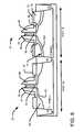
- FIGS. 1 through 10are cross sectional views for illustrating a structure and method for manufacturing a first FET with raised Source/Drain structures and a second FET with embedded SiGe in PFET according to an example embodiment of the present invention.
- the example embodiments of the present inventionwill be described in detail with reference to the accompanying drawings.
- the example embodimentsprovide a method of forming a PFET with embedded S/D stressor regions, and raised S/Ds in the NFET.
- a stress linercan be formed over reduced spacers of the FET gate.
- NFET gate structure 22over a NFET region 16 in a substrate 10 and PFET gate structure 20 over a PFET region 14 .
- the NFET gate structure 22is comprised of a NFET gate dielectric 32 , a NFET gate 36 , NFET gate cap layer 40 over the NFET gate 36 , NFET first (L-shaped) spacers 44 , and NFET second spacers 50 .
- the gate cap layer 40can be comprised of silicon nitride.
- the NFET second spacers 50can be comprised of silicon nitride.
- the PFET gate structure 20is preferably comprised of a PFET gate dielectric 30 , a PFET gate 34 , PFET gate cap layer 38 comprised of silicon nitride, PFET first (L-shaped) spacers 42 , and PFET second spacers 52 .
- the PFET second spacers 52can be comprised of silicon nitride.
- NFET Source/drain extensionSDE
- LDDlightly doped drain
- isolation regions 18 between the PFET region 14 and the NFET region 16are preferably STI regions comprised of silicon oxide.
- the structurecan have a Pwell 17 in the NFET region 16 and a Nwell 15 in the PFET region 14 .
- PFET devicesare formed in the PFET region.
- NFET devicesare formed in the NFET region.
- FIGS. 2 and 3show an example process for forming the recesses 70 .
- the dielectric layer 64is preferably conformal in nature and comprised of a low temperature oxide layer.
- the thickness of the dielectric layer 64can be between 80 to 350 Angstroms.
- the dielectric layerwill be used as an etch mask for the subsequent S/D recess etch.
- a wet etch processis preferred; the wet etch can be comprised of a buffered HF etch.
- RIEetch chemistry
- the etch chemistryis chosen such that it is highly selective to the materials surrounding the gate structures 22 and 20 . In this way, the oxide and nitride spacers surrounding the gate structures 22 and 20 are not etched or are etched to a minimum extent.
- the recesses 70preferably have a depth between 30 and 150 nm.
- the epitaxy pre-cleanpreferably is comprised of HF, either in the gaseous or liquid state, or a combination of steps and chemicals that include the gaseous HF or liquid HF.
- PFET embedded (e.g., B doped SiGe) stressorin the source/drain region 74 .
- the silicon-germanium alloyforms a lattice-mismatched region with the adjacent Si substrate 70 , and this causes strain to be imparted in the channel direction.
- the lattice-mismatched regionis formed using an epitaxial growth process such as chemical vapor deposition, ultra-high vacuum chemical vapor deposition, or molecular beam epitaxy.
- the epitaxy processis selective because SiGe only grows on exposed Si regions and not on the oxide or nitride protected gate.
- the SiGe stressoris preferably in-situ doped with B.
- the Ge concentration in the SiGe alloyis between 10 and 40 atomic percent.
- the boron concentration in the SiGe alloyis between 8E19/cm3 to 1E21/cm3.
- the PFET embedded Source/drain stressor 74is formed to put a stress on the PFET channel region to improve device performance.
- the dielectric layer 64 over the NFET region 16protects the NFET from SiGe epitaxial growth. If the dielectric layer 64 over the gate structures is not adequate to protect the NFET gate 36 , for example, it may be thinned down or removed during the epitaxial preclean step, the NFET gate cap layer 40 prevents SiGe epitaxial growth in the NFET gate 36 .
- the PFET gate cap layer 38 and PFET first spacers 42protect the poly-Si gate 34 from SiGe epitaxial growth.
- a dielectrice.g., oxide
- NFET S/D epitaxial Si layer 79over the NFET SDE regions 58 and a PFET S/D epitaxial Si layer 75 over PFET embedded (B doped SiGe) source/drain stressor 74 .
- the NFET S/D epitaxial Si layer 79can be thicker than that of PFET S/D epitaxial Si layer 75 because the epitaxial Si grows faster over the Si substrate than over the embedded (SiGe) S/D 74 .
- the reasonis that when Si grows over a Si surface, homo-epitaxy occurs, as opposed to Si growing over a SiGe surface (hetero-epitaxy occurs).
- the growth ratecan also be controlled by the epitaxy process conditions.
- the NFET gate cap layer 40 and PFET gate cap layer 38protects the poly-Si gate from the Si epitaxial growth.
- the epitaxial Sigrows between 5% and 20% thicker over the Si Substrate than over the SiGe S/D 74 .
- the NFET S/D epitaxial Si layer 79has a thickness between 50 and 500 angstroms and the PFET S/D epitaxial Si layer 75 can have a thickness between 40 and 400 angstroms.
- the NFET S/D epitaxial Si layer 79is thicker than that PFET S/D epitaxial Si layer 75 (e.g., between 5% and 20% thicker). This is because typically, when we grow SiGe stressor 74 , there will be an overgrowth above the substrate so that it forms a raised S/D structure. At this point the NFET surface is still not raised. By being able to grow a thicker Si layer 79 in the NFET, the final structure is such that both NFET and PFET has the almost the same level of raised S/D structure. This provides a greater process margin for the subsequent contact opening/RIE step.
- Part of the NFET S/D epitaxial Si layer 79 and more preferably the entire PFET S/D epitaxial Si layer 75will be consumed in a subsequent salicide step.
- the NFET S/D epitaxial Si layer 79 and PFET S/D epitaxial Si layer 75reduce or prevent the NFET S/D and the PFET S/D junctions from being thinned and consumed in the subsequent salicide process.
- the NFET S/D epitaxial Si layer 79 and PFET S/D epitaxial Si layer 75help to create the raised S/D structures, thus reducing the external resistance and S/D sheet resistance, which in turn will improve device performance of both NFET and PFET.
- the PFET S/D epitaxial Si layer 75is doped by outdiffusing of B from the embedded S/D stressor region 74 during a subsequent anneal.
- the PFET S/D epitaxial Si layer (Si cap layer) 75 over the embedded Source/drain stressor 74will be consumed in a subsequent salicide step, it acts as a sacrificial layer for the PFET embedded Source/drain stressor 74 to form a stable and low resistivity silicide. This is because SiGe alone usually does not form a low resistivity silicide with the typical metallic materials (e.g. Co, Ti, Ni or NiPt), and/or the silicide formed has poor surface and interface roughness. This is an advantage of the Si cap 75 over PFET embedded stressor Source/drain 74 .
- the etchis preferably a nitride wet etch.
- the wet etchcan be comprised of a hot phosphoric acid etch.
- Preferably the second PFET spacers 52 and the second NFET spacer 50are completely removed.
- reduced second PFET spacers 53 and reduced second NFET spacer 51are preferably comprised of nitride.
- the spacerare called reduced because the have a reduce height and width compared to the original second spacer. This is an advantage because the reduced spacers allow the stress from a subsequently formed overlying stress liner to be transmitted to the channel.
- the second reduced spacerscan be 30 to 70% smaller in terms of height and/or width compared to the original second spacer.
- the PFET S/D epitaxial Si layer 75is doped by the outdiffusion of impurities (boron) from the embedded S/D 74 .
- the annealis preferably performed at a temperature between 900 C and 1350 C for a time between 10 microsec and 5 sec.
- the annealis preferably a spike anneal.
- the P-type dopant from the embedded S/D 74diffuses down into the substrate to form final PFET S/D junctions 74 A.
- silicidecan be formed over the gates and source/drain regions.
- gate silicide layer 84 and raised S/D silicide layer 86are formed over NFET gate 36 and NFET raised S/D 60 79 .
- gate silicide layer 88 and S/D silicide layer 90is formed over PFET gate 34 and stressor regions 74 (and Si epitaxial layer 75 if not totally consumed by the silicide process).
- silicidewe first deposit a metal layer such as essentially Ni, Pt, NiPt, NiPd or Co, or combinations thereof and most preferably NiPt over the substrate surface, the NFET region 16 and the PFET region 14 . Then, we anneal the substrate 10 to convert the metal to metal-silicides. We remove the unreacted metal layer with a selective metal etch process (preferably wet etch). After this step, an optional heat treatment is performed to form metal-silicides of desired silicide phases with low sheet resistance values.
- a metal layersuch as essentially Ni, Pt, NiPt, NiPd or Co, or combinations thereof and most preferably NiPt over the substrate surface, the NFET region 16 and the PFET region 14 . Then, we anneal the substrate 10 to convert the metal to metal-silicides. We remove the unreacted metal layer with a selective metal etch process (preferably wet etch). After this step, an optional heat treatment is performed to form metal-silicides of desired
- Subsequent processingcan continue, (see FIG. 10 ) such as the formation: of a stress liner (e.g., SiN) 92 over the substrate and FET devices.
- the stress linercan create a compressive stress on the PFET channel.
- the reduced width PFET spacers 53 on the PFET gatecan increase the compressive stress to the PFET channel.
Landscapes
- Insulated Gate Type Field-Effect Transistor (AREA)
Abstract
Description
Claims (24)
Priority Applications (1)
| Application Number | Priority Date | Filing Date | Title |
|---|---|---|---|
| US12/780,962US8288825B2 (en) | 2005-12-16 | 2010-05-17 | Formation of raised source/drain structures in NFET with embedded SiGe in PFET |
Applications Claiming Priority (2)
| Application Number | Priority Date | Filing Date | Title |
|---|---|---|---|
| US11/305,584US7718500B2 (en) | 2005-12-16 | 2005-12-16 | Formation of raised source/drain structures in NFET with embedded SiGe in PFET |
| US12/780,962US8288825B2 (en) | 2005-12-16 | 2010-05-17 | Formation of raised source/drain structures in NFET with embedded SiGe in PFET |
Related Parent Applications (1)
| Application Number | Title | Priority Date | Filing Date |
|---|---|---|---|
| US11/305,584DivisionUS7718500B2 (en) | 2005-12-16 | 2005-12-16 | Formation of raised source/drain structures in NFET with embedded SiGe in PFET |
Publications (2)
| Publication Number | Publication Date |
|---|---|
| US20100219485A1 US20100219485A1 (en) | 2010-09-02 |
| US8288825B2true US8288825B2 (en) | 2012-10-16 |
Family
ID=38172475
Family Applications (2)
| Application Number | Title | Priority Date | Filing Date |
|---|---|---|---|
| US11/305,584Active2028-04-28US7718500B2 (en) | 2005-12-16 | 2005-12-16 | Formation of raised source/drain structures in NFET with embedded SiGe in PFET |
| US12/780,962ActiveUS8288825B2 (en) | 2005-12-16 | 2010-05-17 | Formation of raised source/drain structures in NFET with embedded SiGe in PFET |
Family Applications Before (1)
| Application Number | Title | Priority Date | Filing Date |
|---|---|---|---|
| US11/305,584Active2028-04-28US7718500B2 (en) | 2005-12-16 | 2005-12-16 | Formation of raised source/drain structures in NFET with embedded SiGe in PFET |
Country Status (3)
| Country | Link |
|---|---|
| US (2) | US7718500B2 (en) |
| KR (1) | KR100781541B1 (en) |
| SG (3) | SG133479A1 (en) |
Cited By (8)
| Publication number | Priority date | Publication date | Assignee | Title |
|---|---|---|---|---|
| US20120156846A1 (en)* | 2010-12-16 | 2012-06-21 | Globalfoundries Inc. | Semiconductor Devices Comprising a Channel Semiconductor Alloy Formed with Reduced STI Topography |
| US8841189B1 (en) | 2013-06-14 | 2014-09-23 | International Business Machines Corporation | Transistor having all-around source/drain metal contact channel stressor and method to fabricate same |
| US8889552B2 (en) | 2013-03-04 | 2014-11-18 | Samsung Electronics Co., Ltd. | Semiconductor device having dual metal silicide layers and method of manufacturing the same |
| US9595610B2 (en) | 2014-07-07 | 2017-03-14 | Samsung Electronics Co., Ltd. | Field effect transistor and method of fabricating the same |
| US9607989B2 (en)* | 2014-12-04 | 2017-03-28 | Globalfoundries Inc. | Forming self-aligned NiSi placement with improved performance and yield |
| US10224213B2 (en) | 2016-04-28 | 2019-03-05 | Samsung Electronics Co., Ltd. | Method for forming patterns of a semiconductor device |
| US11764225B2 (en) | 2021-06-10 | 2023-09-19 | Globalfoundries U.S. Inc. | Field effect transistor with shallow trench isolation features within source/drain regions |
| US12142686B2 (en) | 2021-05-26 | 2024-11-12 | Globalfoundries U.S. Inc. | Field effect transistor |
Families Citing this family (86)
| Publication number | Priority date | Publication date | Assignee | Title |
|---|---|---|---|---|
| CN1941296A (en)* | 2005-09-28 | 2007-04-04 | 中芯国际集成电路制造(上海)有限公司 | In-situ silicon-germanium doped and silicon carbide source leakage pole area for strain silicon CMOS transistor |
| CN100442476C (en) | 2005-09-29 | 2008-12-10 | 中芯国际集成电路制造(上海)有限公司 | Strain-induced mobility-enhanced nanodevices and processes for CMOS technology |
| US7718500B2 (en)* | 2005-12-16 | 2010-05-18 | Chartered Semiconductor Manufacturing, Ltd | Formation of raised source/drain structures in NFET with embedded SiGe in PFET |
| US7811913B2 (en)* | 2005-12-19 | 2010-10-12 | Sharp Laboratories Of America, Inc. | Method of fabricating a low, dark-current germanium-on-silicon pin photo detector |
| US20070184600A1 (en)* | 2006-02-06 | 2007-08-09 | Freescale Semiconductor | Stressed-channel CMOS transistors |
| US7446026B2 (en)* | 2006-02-08 | 2008-11-04 | Freescale Semiconductor, Inc. | Method of forming a CMOS device with stressor source/drain regions |
| US7691698B2 (en)* | 2006-02-21 | 2010-04-06 | International Business Machines Corporation | Pseudomorphic Si/SiGe/Si body device with embedded SiGe source/drain |
| US7442619B2 (en)* | 2006-05-18 | 2008-10-28 | International Business Machines Corporation | Method of forming substantially L-shaped silicide contact for a semiconductor device |
| US7439120B2 (en)* | 2006-08-11 | 2008-10-21 | Advanced Micro Devices, Inc. | Method for fabricating stress enhanced MOS circuits |
| US7416931B2 (en)* | 2006-08-22 | 2008-08-26 | Advanced Micro Devices, Inc. | Methods for fabricating a stress enhanced MOS circuit |
| US7442601B2 (en)* | 2006-09-18 | 2008-10-28 | Advanced Micro Devices, Inc. | Stress enhanced CMOS circuits and methods for their fabrication |
| JP5114919B2 (en)* | 2006-10-26 | 2013-01-09 | 富士通セミコンダクター株式会社 | Semiconductor device and manufacturing method thereof |
| US8008157B2 (en)* | 2006-10-27 | 2011-08-30 | Taiwan Semiconductor Manufacturing Company, Ltd. | CMOS device with raised source and drain regions |
| US8569837B2 (en)* | 2007-05-07 | 2013-10-29 | Taiwan Semiconductor Manufacturing Company, Ltd. | MOS devices having elevated source/drain regions |
| KR100844933B1 (en)* | 2007-06-26 | 2008-07-09 | 주식회사 하이닉스반도체 | Transistor of semiconductor device and manufacturing method thereof |
| CN101364545B (en)* | 2007-08-10 | 2010-12-22 | 中芯国际集成电路制造(上海)有限公司 | Germanium-silicon and polycrystalline silicon grating construction of strain silicon transistor |
| US7781799B2 (en)* | 2007-10-24 | 2010-08-24 | Taiwan Semiconductor Manufacturing Company, Ltd. | Source/drain strained layers |
| KR101197464B1 (en) | 2007-12-26 | 2012-11-09 | 삼성전자주식회사 | Method of manufacturing a semiconductor device |
| US7998835B2 (en)* | 2008-01-15 | 2011-08-16 | Globalfoundries Singapore Pte. Ltd. | Strain-direct-on-insulator (SDOI) substrate and method of forming |
| US20090184341A1 (en)* | 2008-01-17 | 2009-07-23 | Chartered Semiconductor Manufacturing, Ltd. | Elimination of STI recess and facet growth in embedded silicon-germanium (eSiGe) module |
| US20090186475A1 (en)* | 2008-01-21 | 2009-07-23 | Shyh-Fann Ting | Method of manufacturing a MOS transistor |
| US8122394B2 (en)* | 2008-09-17 | 2012-02-21 | Taiwan Semiconductor Manufacturing Company, Ltd. | Performance-aware logic operations for generating masks |
| DE102008030854B4 (en)* | 2008-06-30 | 2014-03-20 | Advanced Micro Devices, Inc. | MOS transistors having depressed drain and source regions and non-conforming metal silicide regions, and methods of fabricating the transistors |
| DE102008054075B4 (en)* | 2008-10-31 | 2010-09-23 | Advanced Micro Devices, Inc., Sunnyvale | Semiconductor device having a lowered drain and source region in conjunction with a method of complex silicide fabrication in transistors |
| US8003467B2 (en)* | 2008-11-03 | 2011-08-23 | Taiwan Semiconductor Manufacturing Company, Ltd. | Method for making a semiconductor device having metal gate stacks |
| KR101561059B1 (en)* | 2008-11-20 | 2015-10-16 | 삼성전자주식회사 | Semiconductor device and method of forming the same |
| US8957482B2 (en) | 2009-03-31 | 2015-02-17 | Taiwan Semiconductor Manufacturing Company, Ltd. | Electrical fuse and related applications |
| DE102009015715B4 (en)* | 2009-03-31 | 2011-03-17 | Globalfoundries Dresden Module One Llc & Co. Kg | A method of fabricating a transistor device while maintaining the integrity of a high-k gate stack through an offset spacer used to determine a spacing of a strain-inducing semiconductor alloy and transistor device |
| US8912602B2 (en) | 2009-04-14 | 2014-12-16 | Taiwan Semiconductor Manufacturing Company, Ltd. | FinFETs and methods for forming the same |
| US8440517B2 (en) | 2010-10-13 | 2013-05-14 | Taiwan Semiconductor Manufacturing Company, Ltd. | FinFET and method of fabricating the same |
| US8264032B2 (en) | 2009-09-01 | 2012-09-11 | Taiwan Semiconductor Manufacturing Company, Ltd. | Accumulation type FinFET, circuits and fabrication method thereof |
| US8497528B2 (en) | 2010-05-06 | 2013-07-30 | Taiwan Semiconductor Manufacturing Company, Ltd. | Method for fabricating a strained structure |
| US9484462B2 (en) | 2009-09-24 | 2016-11-01 | Taiwan Semiconductor Manufacturing Company, Ltd. | Fin structure of fin field effect transistor |
| US8623728B2 (en)* | 2009-07-28 | 2014-01-07 | Taiwan Semiconductor Manufacturing Company, Ltd. | Method for forming high germanium concentration SiGe stressor |
| US8980719B2 (en) | 2010-04-28 | 2015-03-17 | Taiwan Semiconductor Manufacturing Company, Ltd. | Methods for doping fin field-effect transistors |
| US8106456B2 (en)* | 2009-07-29 | 2012-01-31 | International Business Machines Corporation | SOI transistors having an embedded extension region to improve extension resistance and channel strain characteristics |
| US8048765B2 (en)* | 2009-08-28 | 2011-11-01 | Broadcom Corporation | Method for fabricating a MOS transistor with source/well heterojunction and related structure |
| US20110049582A1 (en)* | 2009-09-03 | 2011-03-03 | International Business Machines Corporation | Asymmetric source and drain stressor regions |
| CN102024761A (en)* | 2009-09-18 | 2011-04-20 | 中芯国际集成电路制造(上海)有限公司 | Method for forming semiconductor integrated circuit device |
| US8404538B2 (en)* | 2009-10-02 | 2013-03-26 | Taiwan Semiconductor Manufacturing Co., Ltd. | Device with self aligned stressor and method of making same |
| US8035141B2 (en)* | 2009-10-28 | 2011-10-11 | International Business Machines Corporation | Bi-layer nFET embedded stressor element and integration to enhance drive current |
| US20110127614A1 (en)* | 2009-11-30 | 2011-06-02 | Thilo Scheiper | Reducing the series resistance in sophisticated transistors by embedding metal silicide contact regions reliably into highly doped semiconductor material |
| JP5452211B2 (en)* | 2009-12-21 | 2014-03-26 | ルネサスエレクトロニクス株式会社 | Semiconductor device and method for manufacturing semiconductor device |
| DE102009055435B4 (en)* | 2009-12-31 | 2017-11-09 | Globalfoundries Dresden Module One Limited Liability Company & Co. Kg | Increased inclusion of high-k metal gate electrode structures by reducing material erosion of a dielectric cap layer in forming a strain-inducing semiconductor alloy |
| US8765532B2 (en)* | 2010-01-11 | 2014-07-01 | International Business Machines Corporation | Fabrication of field effect devices using spacers |
| US9040393B2 (en) | 2010-01-14 | 2015-05-26 | Taiwan Semiconductor Manufacturing Company, Ltd. | Method of forming semiconductor structure |
| JP2011181686A (en)* | 2010-03-01 | 2011-09-15 | Renesas Electronics Corp | Semiconductor device and method of manufacturing the same |
| US8236660B2 (en) | 2010-04-21 | 2012-08-07 | International Business Machines Corporation | Monolayer dopant embedded stressor for advanced CMOS |
| US8426278B2 (en)* | 2010-06-09 | 2013-04-23 | GlobalFoundries, Inc. | Semiconductor devices having stressor regions and related fabrication methods |
| US8299535B2 (en) | 2010-06-25 | 2012-10-30 | International Business Machines Corporation | Delta monolayer dopants epitaxy for embedded source/drain silicide |
| CN102376769B (en)* | 2010-08-18 | 2013-06-26 | 中国科学院微电子研究所 | Ultra-thin body transistor and manufacturing method thereof |
| US8928094B2 (en)* | 2010-09-03 | 2015-01-06 | Taiwan Semiconductor Manufacturing Company, Ltd. | Strained asymmetric source/drain |
| KR101776926B1 (en)* | 2010-09-07 | 2017-09-08 | 삼성전자주식회사 | Semiconductor device and method for manufacturing the same |
| US8603924B2 (en) | 2010-10-19 | 2013-12-10 | Taiwan Semiconductor Manufacturing Company, Ltd. | Methods of forming gate dielectric material |
| KR101796116B1 (en) | 2010-10-20 | 2017-11-10 | 삼성전자 주식회사 | Semiconductor device, memory module and memory system having the same and operating method thereof |
| US9048181B2 (en) | 2010-11-08 | 2015-06-02 | Taiwan Semiconductor Manufacturing Company, Ltd. | Mechanisms for forming ultra shallow junction |
| US8769446B2 (en) | 2010-11-12 | 2014-07-01 | Taiwan Semiconductor Manufacturing Company, Ltd. | Method and device for increasing fin device density for unaligned fins |
| DE102010063298B4 (en)* | 2010-12-16 | 2012-08-16 | Globalfoundries Dresden Module One Limited Liability Company & Co. Kg | Structuring a strained dielectric material in a contact plane without using a remaining etch stop layer |
| US8877602B2 (en) | 2011-01-25 | 2014-11-04 | Taiwan Semiconductor Manufacturing Company, Ltd. | Mechanisms of doping oxide for forming shallow trench isolation |
| US8592915B2 (en) | 2011-01-25 | 2013-11-26 | Taiwan Semiconductor Manufacturing Company, Ltd. | Doped oxide for shallow trench isolation (STI) |
| US9269634B2 (en)* | 2011-05-16 | 2016-02-23 | Globalfoundries Inc. | Self-aligned metal gate CMOS with metal base layer and dummy gate structure |
| US9087741B2 (en) | 2011-07-11 | 2015-07-21 | International Business Machines Corporation | CMOS with dual raised source and drain for NMOS and PMOS |
| US9012286B2 (en)* | 2012-04-12 | 2015-04-21 | Globalfoundries Inc. | Methods of forming FinFET semiconductor devices so as to tune the threshold voltage of such devices |
| JP5927017B2 (en)* | 2012-04-20 | 2016-05-25 | ルネサスエレクトロニクス株式会社 | Semiconductor device and manufacturing method of semiconductor device |
| US8962433B2 (en) | 2012-06-12 | 2015-02-24 | United Microelectronics Corp. | MOS transistor process |
| US8987093B2 (en) | 2012-09-20 | 2015-03-24 | International Business Machines Corporation | Multigate finFETs with epitaxially-grown merged source/drains |
| JP6094159B2 (en)* | 2012-11-13 | 2017-03-15 | 三菱電機株式会社 | Manufacturing method of semiconductor device |
| US20140183663A1 (en)* | 2012-12-28 | 2014-07-03 | Texas Instruments Incorporated | Raised Source/Drain MOS Transistor and Method of Forming the Transistor with an Implant Spacer and an Epitaxial Spacer |
| CN104103590B (en)* | 2013-04-15 | 2017-05-17 | 中芯国际集成电路制造(上海)有限公司 | Semiconductor device manufacturing method |
| CN103337452A (en)* | 2013-06-26 | 2013-10-02 | 上海华力微电子有限公司 | Process method for forming nickel salicide on silicon germanium layer |
| US9245955B2 (en) | 2013-06-28 | 2016-01-26 | Stmicroelectronics, Inc. | Embedded shape SiGe for strained channel transistors |
| US9276113B2 (en) | 2014-03-10 | 2016-03-01 | International Business Corporation | Structure and method to make strained FinFET with improved junction capacitance and low leakage |
| US9184179B2 (en) | 2014-03-21 | 2015-11-10 | International Business Machines Corporation | Thin channel-on-insulator MOSFET device with n+ epitaxy substrate and embedded stressor |
| US9362128B2 (en) | 2014-04-22 | 2016-06-07 | Globalfoundries Singapore Pte. Ltd. | Methods for fabricating integrated circuits and components thereof |
| US10084063B2 (en)* | 2014-06-23 | 2018-09-25 | Taiwan Semiconductor Manufacturing Company Ltd. | Semiconductor device and manufacturing method thereof |
| US9502418B2 (en)* | 2014-10-02 | 2016-11-22 | International Business Machines Corporation | Semiconductor devices with sidewall spacers of equal thickness |
| US9324623B1 (en) | 2014-11-26 | 2016-04-26 | Samsung Electronics Co., Ltd. | Method of manufacturing semiconductor device having active fins |
| US9508718B2 (en) | 2014-12-29 | 2016-11-29 | Taiwan Semiconductor Manufacturing Company, Ltd. | FinFET contact structure and method for forming the same |
| US9484255B1 (en) | 2015-11-03 | 2016-11-01 | International Business Machines Corporation | Hybrid source and drain contact formation using metal liner and metal insulator semiconductor contacts |
| US9972682B2 (en)* | 2016-01-22 | 2018-05-15 | International Business Machines Corporation | Low resistance source drain contact formation |
| US10269714B2 (en) | 2016-09-06 | 2019-04-23 | International Business Machines Corporation | Low resistance contacts including intermetallic alloy of nickel, platinum, titanium, aluminum and type IV semiconductor elements |
| US10332750B2 (en) | 2017-11-22 | 2019-06-25 | United Microelectronics Corp. | Method for fabricating semiconductor device with strained silicon structure |
| US10861753B2 (en)* | 2018-10-30 | 2020-12-08 | Taiwan Semiconductor Manufacturing Co., Ltd. | Air gap formation between gate spacer and epitaxy structure |
| US11031502B2 (en) | 2019-01-08 | 2021-06-08 | Samsung Electronics Co., Ltd. | Semiconductor devices |
| US11239363B2 (en)* | 2019-01-08 | 2022-02-01 | Samsung Electronics Co., Ltd. | Semiconductor devices |
| KR20230164472A (en) | 2022-05-25 | 2023-12-04 | 삼성전자주식회사 | Integrated circuit device |
Citations (18)
| Publication number | Priority date | Publication date | Assignee | Title |
|---|---|---|---|---|
| US5824586A (en)* | 1996-10-23 | 1998-10-20 | Advanced Micro Devices, Inc. | Method of manufacturing a raised source/drain MOSFET |
| US6159815A (en) | 1996-09-27 | 2000-12-12 | Siemens Aktiengesellschaft | Method of producing a MOS transistor |
| JP2001284468A (en) | 2000-03-30 | 2001-10-12 | Toshiba Corp | Semiconductor device and method of manufacturing the same |
| US6531347B1 (en) | 2000-02-08 | 2003-03-11 | Advanced Micro Devices, Inc. | Method of making recessed source drains to reduce fringing capacitance |
| US6744104B1 (en)* | 1998-11-17 | 2004-06-01 | Kabushiki Kaisha Toshiba | Semiconductor integrated circuit including insulated gate field effect transistor and method of manufacturing the same |
| US20040262683A1 (en) | 2003-06-27 | 2004-12-30 | Bohr Mark T. | PMOS transistor strain optimization with raised junction regions |
| US6849883B2 (en) | 2002-09-02 | 2005-02-01 | Oki Electric Industry Co., Ltd. | Strained SOI MOSFET device and method of fabricating same |
| US20050035409A1 (en) | 2003-08-15 | 2005-02-17 | Chih-Hsin Ko | Structure and method of a strained channel transistor and a second semiconductor component in an integrated circuit |
| US6861318B2 (en) | 2001-11-01 | 2005-03-01 | Intel Corporation | Semiconductor transistor having a stressed channel |
| US20050079692A1 (en) | 2003-10-10 | 2005-04-14 | Applied Materials, Inc. | Methods to fabricate MOSFET devices using selective deposition process |
| US6881635B1 (en) | 2004-03-23 | 2005-04-19 | International Business Machines Corporation | Strained silicon NMOS devices with embedded source/drain |
| US6906360B2 (en) | 2003-09-10 | 2005-06-14 | International Business Machines Corporation | Structure and method of making strained channel CMOS transistors having lattice-mismatched epitaxial extension and source and drain regions |
| KR20050121479A (en) | 2004-06-22 | 2005-12-27 | 삼성전자주식회사 | Fabricating method of cmos transistor and cmos transistor fabricated by the same method |
| US7176110B2 (en)* | 2003-10-31 | 2007-02-13 | Advanced Micro Devices, Inc. | Technique for forming transistors having raised drain and source regions with different heights |
| US7176522B2 (en)* | 2003-11-25 | 2007-02-13 | Taiwan Semiconductor Manufacturing Company, Ltd. | Semiconductor device having high drive current and method of manufacturing thereof |
| US7348248B2 (en) | 2005-07-12 | 2008-03-25 | Taiwan Semiconductor Manufacturing Company, Ltd. | CMOS transistor with high drive current and low sheet resistance |
| US7407860B2 (en)* | 2004-05-26 | 2008-08-05 | Fujitsu Limited | Method of fabricating a complementary semiconductor device having a strained channel p-transistor |
| US7718500B2 (en)* | 2005-12-16 | 2010-05-18 | Chartered Semiconductor Manufacturing, Ltd | Formation of raised source/drain structures in NFET with embedded SiGe in PFET |
- 2005
- 2005-12-16USUS11/305,584patent/US7718500B2/enactiveActive
- 2006
- 2006-07-13KRKR1020060066004Apatent/KR100781541B1/enactiveActive
- 2006-10-17SGSG200607223-5Apatent/SG133479A1/enunknown
- 2006-10-17SGSG201102172-2Apatent/SG170782A1/enunknown
- 2006-10-17SGSG200903941-3Apatent/SG153817A1/enunknown
- 2010
- 2010-05-17USUS12/780,962patent/US8288825B2/enactiveActive
Patent Citations (19)
| Publication number | Priority date | Publication date | Assignee | Title |
|---|---|---|---|---|
| US6159815A (en) | 1996-09-27 | 2000-12-12 | Siemens Aktiengesellschaft | Method of producing a MOS transistor |
| US5824586A (en)* | 1996-10-23 | 1998-10-20 | Advanced Micro Devices, Inc. | Method of manufacturing a raised source/drain MOSFET |
| US6744104B1 (en)* | 1998-11-17 | 2004-06-01 | Kabushiki Kaisha Toshiba | Semiconductor integrated circuit including insulated gate field effect transistor and method of manufacturing the same |
| US6531347B1 (en) | 2000-02-08 | 2003-03-11 | Advanced Micro Devices, Inc. | Method of making recessed source drains to reduce fringing capacitance |
| JP2001284468A (en) | 2000-03-30 | 2001-10-12 | Toshiba Corp | Semiconductor device and method of manufacturing the same |
| US6861318B2 (en) | 2001-11-01 | 2005-03-01 | Intel Corporation | Semiconductor transistor having a stressed channel |
| US6849883B2 (en) | 2002-09-02 | 2005-02-01 | Oki Electric Industry Co., Ltd. | Strained SOI MOSFET device and method of fabricating same |
| US20040262683A1 (en) | 2003-06-27 | 2004-12-30 | Bohr Mark T. | PMOS transistor strain optimization with raised junction regions |
| US20050035409A1 (en) | 2003-08-15 | 2005-02-17 | Chih-Hsin Ko | Structure and method of a strained channel transistor and a second semiconductor component in an integrated circuit |
| US6906360B2 (en) | 2003-09-10 | 2005-06-14 | International Business Machines Corporation | Structure and method of making strained channel CMOS transistors having lattice-mismatched epitaxial extension and source and drain regions |
| US20050079692A1 (en) | 2003-10-10 | 2005-04-14 | Applied Materials, Inc. | Methods to fabricate MOSFET devices using selective deposition process |
| US7176110B2 (en)* | 2003-10-31 | 2007-02-13 | Advanced Micro Devices, Inc. | Technique for forming transistors having raised drain and source regions with different heights |
| US7176522B2 (en)* | 2003-11-25 | 2007-02-13 | Taiwan Semiconductor Manufacturing Company, Ltd. | Semiconductor device having high drive current and method of manufacturing thereof |
| US6881635B1 (en) | 2004-03-23 | 2005-04-19 | International Business Machines Corporation | Strained silicon NMOS devices with embedded source/drain |
| US7407860B2 (en)* | 2004-05-26 | 2008-08-05 | Fujitsu Limited | Method of fabricating a complementary semiconductor device having a strained channel p-transistor |
| KR20050121479A (en) | 2004-06-22 | 2005-12-27 | 삼성전자주식회사 | Fabricating method of cmos transistor and cmos transistor fabricated by the same method |
| US7354835B2 (en) | 2004-06-22 | 2008-04-08 | Samsung Electronics Co., Ltd. | Method of fabricating CMOS transistor and CMOS transistor fabricated thereby |
| US7348248B2 (en) | 2005-07-12 | 2008-03-25 | Taiwan Semiconductor Manufacturing Company, Ltd. | CMOS transistor with high drive current and low sheet resistance |
| US7718500B2 (en)* | 2005-12-16 | 2010-05-18 | Chartered Semiconductor Manufacturing, Ltd | Formation of raised source/drain structures in NFET with embedded SiGe in PFET |
Non-Patent Citations (1)
| Title |
|---|
| Gene Fitzgerald, A Quick Primer on Strained Silicon, URL: http://www.eetimes.com/showArticle.jhtml?articleID=18100036, Time: Feb. 23, 2004, 12:00 PM EST. |
Cited By (12)
| Publication number | Priority date | Publication date | Assignee | Title |
|---|---|---|---|---|
| US20120156846A1 (en)* | 2010-12-16 | 2012-06-21 | Globalfoundries Inc. | Semiconductor Devices Comprising a Channel Semiconductor Alloy Formed with Reduced STI Topography |
| US8748275B2 (en)* | 2010-12-16 | 2014-06-10 | Globalfoundries Inc. | Semiconductor devices comprising a channel semiconductor alloy formed with reduced STI topography |
| US8889552B2 (en) | 2013-03-04 | 2014-11-18 | Samsung Electronics Co., Ltd. | Semiconductor device having dual metal silicide layers and method of manufacturing the same |
| US9117692B2 (en) | 2013-03-04 | 2015-08-25 | Samsung Electronics Co., Ltd. | Semiconductor device having dual metal silicide layers and method of manufacturing the same |
| US8841189B1 (en) | 2013-06-14 | 2014-09-23 | International Business Machines Corporation | Transistor having all-around source/drain metal contact channel stressor and method to fabricate same |
| US8901672B1 (en) | 2013-06-14 | 2014-12-02 | International Business Machines Corporation | Transistor having all-around source/drain metal contact channel stressor and method to fabricate same |
| US9595610B2 (en) | 2014-07-07 | 2017-03-14 | Samsung Electronics Co., Ltd. | Field effect transistor and method of fabricating the same |
| US9607989B2 (en)* | 2014-12-04 | 2017-03-28 | Globalfoundries Inc. | Forming self-aligned NiSi placement with improved performance and yield |
| US10224213B2 (en) | 2016-04-28 | 2019-03-05 | Samsung Electronics Co., Ltd. | Method for forming patterns of a semiconductor device |
| US12142686B2 (en) | 2021-05-26 | 2024-11-12 | Globalfoundries U.S. Inc. | Field effect transistor |
| US11764225B2 (en) | 2021-06-10 | 2023-09-19 | Globalfoundries U.S. Inc. | Field effect transistor with shallow trench isolation features within source/drain regions |
| US12336285B2 (en) | 2021-06-10 | 2025-06-17 | Globalfoundries U.S. Inc. | Field effect transistor with shallow trench isolation features within source/drain regions |
Also Published As
| Publication number | Publication date |
|---|---|
| SG153817A1 (en) | 2009-07-29 |
| SG170782A1 (en) | 2011-05-30 |
| SG133479A1 (en) | 2007-07-30 |
| US7718500B2 (en) | 2010-05-18 |
| KR100781541B1 (en) | 2007-12-03 |
| US20100219485A1 (en) | 2010-09-02 |
| KR20070064231A (en) | 2007-06-20 |
| US20070138570A1 (en) | 2007-06-21 |
Similar Documents
| Publication | Publication Date | Title |
|---|---|---|
| US8288825B2 (en) | Formation of raised source/drain structures in NFET with embedded SiGe in PFET | |
| US7332439B2 (en) | Metal gate transistors with epitaxial source and drain regions | |
| CN104299971B (en) | MOS device with the distribution of uneven p type impurity | |
| US7208362B2 (en) | Transistor device containing carbon doped silicon in a recess next to MDD to create strain in channel | |
| JP5030774B2 (en) | Transistor formation method | |
| US8405131B2 (en) | High performance MOSFET comprising a stressed gate metal silicide layer and method of fabricating the same | |
| US7060579B2 (en) | Increased drive current by isotropic recess etch | |
| CN102165571B (en) | Method for fabricating MOS devices with highly stressed channels | |
| US7405131B2 (en) | Method and structure to prevent silicide strapping of source/drain to body in semiconductor devices with source/drain stressor | |
| US7122435B2 (en) | Methods, systems and structures for forming improved transistors | |
| US7372099B2 (en) | Semiconductor device and its manufacturing method | |
| US7432559B2 (en) | Silicide formation on SiGe | |
| JP2010505267A (en) | Stress application field effect transistor and method of manufacturing the same | |
| CN101711427A (en) | Strain-strengthened semiconductor device and method for manufacturing same | |
| US20080119025A1 (en) | Method of making a strained semiconductor device | |
| US7582535B2 (en) | Method of forming MOS transistor having fully silicided metal gate electrode | |
| US20080001191A1 (en) | Drain/source extension structure of a field effect transistor with reduced boron diffusion | |
| US20060199343A1 (en) | Method of forming MOS transistor having fully silicided metal gate electrode |
Legal Events
| Date | Code | Title | Description |
|---|---|---|---|
| FEPP | Fee payment procedure | Free format text:PAYOR NUMBER ASSIGNED (ORIGINAL EVENT CODE: ASPN); ENTITY STATUS OF PATENT OWNER: LARGE ENTITY | |
| AS | Assignment | Owner name:CHARTERED SEMICONDUCTOR MANUFACTURING PTE. LTD., S Free format text:CHANGE OF NAME;ASSIGNOR:CHARTERED SEMICONDUCTOR MANUFACTURING LTD.;REEL/FRAME:028939/0851 Effective date:20100115 Owner name:INTERNATIONAL BUSINESS MACHINES CORPORATION (IBM), Free format text:ASSIGNMENT OF ASSIGNORS INTEREST;ASSIGNORS:LUO, ZHIJIONG;HOLT, JUDSON ROBERT;REEL/FRAME:028939/0757 Effective date:20051212 Owner name:GLOBALFOUNDRIES SINGAPORE PTE. LTD., SINGAPORE Free format text:CHANGE OF NAME;ASSIGNOR:CHARTERED SEMICONDUCTOR MANUFACTURING PTE. LTD.;REEL/FRAME:028939/0853 Effective date:20100115 Owner name:CHARTERED SEMICONDUCTOR MANUFACTURING LTD, SINGAPO Free format text:ASSIGNMENT OF ASSIGNORS INTEREST;ASSIGNOR:CHONG, YUNG FU;REEL/FRAME:028939/0795 Effective date:20051212 Owner name:SAMSUNG ELECTRONICS CO., LTD., KOREA, REPUBLIC OF Free format text:ASSIGNMENT OF ASSIGNORS INTEREST;ASSIGNOR:KIM, JOO CHAN;REEL/FRAME:028939/0787 Effective date:20051212 | |
| STCF | Information on status: patent grant | Free format text:PATENTED CASE | |
| CC | Certificate of correction | ||
| AS | Assignment | Owner name:GLOBALFOUNDRIES U.S. 2 LLC, NEW YORK Free format text:ASSIGNMENT OF ASSIGNORS INTEREST;ASSIGNOR:INTERNATIONAL BUSINESS MACHINES CORPORATION;REEL/FRAME:036550/0001 Effective date:20150629 | |
| AS | Assignment | Owner name:GLOBALFOUNDRIES INC., CAYMAN ISLANDS Free format text:ASSIGNMENT OF ASSIGNORS INTEREST;ASSIGNORS:GLOBALFOUNDRIES U.S. 2 LLC;GLOBALFOUNDRIES U.S. INC.;REEL/FRAME:036779/0001 Effective date:20150910 | |
| FPAY | Fee payment | Year of fee payment:4 | |
| AS | Assignment | Owner name:WILMINGTON TRUST, NATIONAL ASSOCIATION, DELAWARE Free format text:SECURITY AGREEMENT;ASSIGNOR:GLOBALFOUNDRIES INC.;REEL/FRAME:049490/0001 Effective date:20181127 | |
| MAFP | Maintenance fee payment | Free format text:PAYMENT OF MAINTENANCE FEE, 8TH YEAR, LARGE ENTITY (ORIGINAL EVENT CODE: M1552); ENTITY STATUS OF PATENT OWNER: LARGE ENTITY Year of fee payment:8 | |
| AS | Assignment | Owner name:GLOBALFOUNDRIES INC., CAYMAN ISLANDS Free format text:RELEASE BY SECURED PARTY;ASSIGNOR:WILMINGTON TRUST, NATIONAL ASSOCIATION;REEL/FRAME:054475/0718 Effective date:20200410 | |
| AS | Assignment | Owner name:TAIWAN SEMICONDUCTOR MANUFACTURING CO., LTD., TAIWAN Free format text:ASSIGNMENT OF ASSIGNORS INTEREST;ASSIGNORS:GLOBALFOUNDRIES INC.;GLOBALFOUNDRIES SINGAPORE PTE. LTD.;REEL/FRAME:054482/0630 Effective date:20200515 | |
| AS | Assignment | Owner name:GLOBALFOUNDRIES INC., CAYMAN ISLANDS Free format text:RELEASE BY SECURED PARTY;ASSIGNOR:WILMINGTON TRUST, NATIONAL ASSOCIATION;REEL/FRAME:054636/0001 Effective date:20201117 | |
| MAFP | Maintenance fee payment | Free format text:PAYMENT OF MAINTENANCE FEE, 12TH YEAR, LARGE ENTITY (ORIGINAL EVENT CODE: M1553); ENTITY STATUS OF PATENT OWNER: LARGE ENTITY Year of fee payment:12 |