US8288795B2 - Thyristor based memory cells, devices and systems including the same and methods for forming the same - Google Patents
Thyristor based memory cells, devices and systems including the same and methods for forming the sameDownload PDFInfo
- Publication number
- US8288795B2 US8288795B2US12/715,889US71588910AUS8288795B2US 8288795 B2US8288795 B2US 8288795B2US 71588910 AUS71588910 AUS 71588910AUS 8288795 B2US8288795 B2US 8288795B2
- Authority
- US
- United States
- Prior art keywords
- thyristor
- memory cells
- disposed
- conductive
- semiconductor device
- Prior art date
- Legal status (The legal status is an assumption and is not a legal conclusion. Google has not performed a legal analysis and makes no representation as to the accuracy of the status listed.)
- Expired - Fee Related, expires
Links
Images


Classifications
- H—ELECTRICITY
- H10—SEMICONDUCTOR DEVICES; ELECTRIC SOLID-STATE DEVICES NOT OTHERWISE PROVIDED FOR
- H10D—INORGANIC ELECTRIC SEMICONDUCTOR DEVICES
- H10D18/00—Thyristors
- H10D18/01—Manufacture or treatment
- H—ELECTRICITY
- H01—ELECTRIC ELEMENTS
- H01L—SEMICONDUCTOR DEVICES NOT COVERED BY CLASS H10
- H01L21/00—Processes or apparatus adapted for the manufacture or treatment of semiconductor or solid state devices or of parts thereof
- H01L21/02—Manufacture or treatment of semiconductor devices or of parts thereof
- H01L21/04—Manufacture or treatment of semiconductor devices or of parts thereof the devices having potential barriers, e.g. a PN junction, depletion layer or carrier concentration layer
- H01L21/18—Manufacture or treatment of semiconductor devices or of parts thereof the devices having potential barriers, e.g. a PN junction, depletion layer or carrier concentration layer the devices having semiconductor bodies comprising elements of Group IV of the Periodic Table or AIIIBV compounds with or without impurities, e.g. doping materials
- H01L21/28—Manufacture of electrodes on semiconductor bodies using processes or apparatus not provided for in groups H01L21/20 - H01L21/268
- H01L21/28008—Making conductor-insulator-semiconductor electrodes
- H01L21/28017—Making conductor-insulator-semiconductor electrodes the insulator being formed after the semiconductor body, the semiconductor being silicon
- H01L21/28026—Making conductor-insulator-semiconductor electrodes the insulator being formed after the semiconductor body, the semiconductor being silicon characterised by the conductor
- H01L21/28088—Making conductor-insulator-semiconductor electrodes the insulator being formed after the semiconductor body, the semiconductor being silicon characterised by the conductor the final conductor layer next to the insulator being a composite, e.g. TiN
- H—ELECTRICITY
- H01—ELECTRIC ELEMENTS
- H01L—SEMICONDUCTOR DEVICES NOT COVERED BY CLASS H10
- H01L21/00—Processes or apparatus adapted for the manufacture or treatment of semiconductor or solid state devices or of parts thereof
- H01L21/02—Manufacture or treatment of semiconductor devices or of parts thereof
- H01L21/04—Manufacture or treatment of semiconductor devices or of parts thereof the devices having potential barriers, e.g. a PN junction, depletion layer or carrier concentration layer
- H01L21/18—Manufacture or treatment of semiconductor devices or of parts thereof the devices having potential barriers, e.g. a PN junction, depletion layer or carrier concentration layer the devices having semiconductor bodies comprising elements of Group IV of the Periodic Table or AIIIBV compounds with or without impurities, e.g. doping materials
- H01L21/30—Treatment of semiconductor bodies using processes or apparatus not provided for in groups H01L21/20 - H01L21/26
- H01L21/31—Treatment of semiconductor bodies using processes or apparatus not provided for in groups H01L21/20 - H01L21/26 to form insulating layers thereon, e.g. for masking or by using photolithographic techniques; After treatment of these layers; Selection of materials for these layers
- H01L21/3205—Deposition of non-insulating-, e.g. conductive- or resistive-, layers on insulating layers; After-treatment of these layers
- H01L21/32051—Deposition of metallic or metal-silicide layers
- H—ELECTRICITY
- H01—ELECTRIC ELEMENTS
- H01L—SEMICONDUCTOR DEVICES NOT COVERED BY CLASS H10
- H01L21/00—Processes or apparatus adapted for the manufacture or treatment of semiconductor or solid state devices or of parts thereof
- H01L21/02—Manufacture or treatment of semiconductor devices or of parts thereof
- H01L21/04—Manufacture or treatment of semiconductor devices or of parts thereof the devices having potential barriers, e.g. a PN junction, depletion layer or carrier concentration layer
- H01L21/18—Manufacture or treatment of semiconductor devices or of parts thereof the devices having potential barriers, e.g. a PN junction, depletion layer or carrier concentration layer the devices having semiconductor bodies comprising elements of Group IV of the Periodic Table or AIIIBV compounds with or without impurities, e.g. doping materials
- H01L21/30—Treatment of semiconductor bodies using processes or apparatus not provided for in groups H01L21/20 - H01L21/26
- H01L21/31—Treatment of semiconductor bodies using processes or apparatus not provided for in groups H01L21/20 - H01L21/26 to form insulating layers thereon, e.g. for masking or by using photolithographic techniques; After treatment of these layers; Selection of materials for these layers
- H01L21/3205—Deposition of non-insulating-, e.g. conductive- or resistive-, layers on insulating layers; After-treatment of these layers
- H01L21/32055—Deposition of semiconductive layers, e.g. poly - or amorphous silicon layers
- H—ELECTRICITY
- H01—ELECTRIC ELEMENTS
- H01L—SEMICONDUCTOR DEVICES NOT COVERED BY CLASS H10
- H01L21/00—Processes or apparatus adapted for the manufacture or treatment of semiconductor or solid state devices or of parts thereof
- H01L21/02—Manufacture or treatment of semiconductor devices or of parts thereof
- H01L21/04—Manufacture or treatment of semiconductor devices or of parts thereof the devices having potential barriers, e.g. a PN junction, depletion layer or carrier concentration layer
- H01L21/18—Manufacture or treatment of semiconductor devices or of parts thereof the devices having potential barriers, e.g. a PN junction, depletion layer or carrier concentration layer the devices having semiconductor bodies comprising elements of Group IV of the Periodic Table or AIIIBV compounds with or without impurities, e.g. doping materials
- H01L21/30—Treatment of semiconductor bodies using processes or apparatus not provided for in groups H01L21/20 - H01L21/26
- H01L21/31—Treatment of semiconductor bodies using processes or apparatus not provided for in groups H01L21/20 - H01L21/26 to form insulating layers thereon, e.g. for masking or by using photolithographic techniques; After treatment of these layers; Selection of materials for these layers
- H01L21/3205—Deposition of non-insulating-, e.g. conductive- or resistive-, layers on insulating layers; After-treatment of these layers
- H01L21/321—After treatment
- H01L21/3213—Physical or chemical etching of the layers, e.g. to produce a patterned layer from a pre-deposited extensive layer
- H01L21/32133—Physical or chemical etching of the layers, e.g. to produce a patterned layer from a pre-deposited extensive layer by chemical means only
- H—ELECTRICITY
- H10—SEMICONDUCTOR DEVICES; ELECTRIC SOLID-STATE DEVICES NOT OTHERWISE PROVIDED FOR
- H10B—ELECTRONIC MEMORY DEVICES
- H10B99/00—Subject matter not provided for in other groups of this subclass
- H10B99/20—Subject matter not provided for in other groups of this subclass comprising memory cells having thyristors
- H—ELECTRICITY
- H10—SEMICONDUCTOR DEVICES; ELECTRIC SOLID-STATE DEVICES NOT OTHERWISE PROVIDED FOR
- H10D—INORGANIC ELECTRIC SEMICONDUCTOR DEVICES
- H10D18/00—Thyristors
- H10D18/40—Thyristors with turn-on by field effect
- H—ELECTRICITY
- H10—SEMICONDUCTOR DEVICES; ELECTRIC SOLID-STATE DEVICES NOT OTHERWISE PROVIDED FOR
- H10D—INORGANIC ELECTRIC SEMICONDUCTOR DEVICES
- H10D64/00—Electrodes of devices having potential barriers
- H10D64/01—Manufacture or treatment
- H—ELECTRICITY
- H10—SEMICONDUCTOR DEVICES; ELECTRIC SOLID-STATE DEVICES NOT OTHERWISE PROVIDED FOR
- H10D—INORGANIC ELECTRIC SEMICONDUCTOR DEVICES
- H10D64/00—Electrodes of devices having potential barriers
- H10D64/20—Electrodes characterised by their shapes, relative sizes or dispositions
- H10D64/27—Electrodes not carrying the current to be rectified, amplified, oscillated or switched, e.g. gates
- H10D64/291—Gate electrodes for thyristors
- H—ELECTRICITY
- H10—SEMICONDUCTOR DEVICES; ELECTRIC SOLID-STATE DEVICES NOT OTHERWISE PROVIDED FOR
- H10D—INORGANIC ELECTRIC SEMICONDUCTOR DEVICES
- H10D84/00—Integrated devices formed in or on semiconductor substrates that comprise only semiconducting layers, e.g. on Si wafers or on GaAs-on-Si wafers
- H10D84/60—Integrated devices formed in or on semiconductor substrates that comprise only semiconducting layers, e.g. on Si wafers or on GaAs-on-Si wafers characterised by the integration of at least one component covered by groups H10D10/00 or H10D18/00, e.g. integration of BJTs
- H—ELECTRICITY
- H10—SEMICONDUCTOR DEVICES; ELECTRIC SOLID-STATE DEVICES NOT OTHERWISE PROVIDED FOR
- H10D—INORGANIC ELECTRIC SEMICONDUCTOR DEVICES
- H10D88/00—Three-dimensional [3D] integrated devices
Definitions
- Embodiments of the present inventionrelate to thyristor-based memory cells, semiconductor devices that include one or more thyristors and methods for forming such memory cells and semiconductor devices.
- Integrated circuit (IC) memory devicesconventionally include static random access memory (SRAM).
- SRAMstatic random access memory
- Conventional SRAMis based on four-transistor memory cells (4T SRAM cells) or six-transistor memory cells (6T SRAM cells) that are compatible with conventional memory elements, such as complementary metal-oxide-semiconductor (CMOS) devices, operate at low voltage levels and perform at relatively high speeds.
- CMOScomplementary metal-oxide-semiconductor
- conventional SRAMconsumes a large cell area that limits high-density design of SRAM.
- thin capacitively-coupled thyristormeans and includes a bi-stable, three-terminal device that includes a four layer structure including a p-type anode region, an n-type base, a p-type base, and an n-type cathode region arranged in a p-n-p-n configuration.
- the thyristormay include two main terminals, an anode and a cathode, and the control terminal, often referred to as the “gate,” which may be attached to the p-type material nearest the cathode.
- Thyristor-based random access memory (T-RAM) cellsdemonstrate faster switching speeds and lower operating voltages in comparison to conventional SRAM cells.
- a thyristor in a memory devicemay be turned on by biasing the gate so that a p-n-p-n channel conducts a current. Once the device is turned on, often referred to as “latched,” the thyristor does not require the gate to be biased to maintain the current conducted between the cathode and the anode. Instead, it will continue to conduct until a minimum holding current is no longer maintained between the anode and cathode, or until the voltage between the anode and the cathode is reversed. Accordingly, the thyristor may function as a switch or diode capable of being switched between an “on” state and an “off” state.
- a conventional T-RAM cell 10includes a vertical thyristor 12 with a vertical surrounding gate 14 as a bi-stable element and an access transistor 16 formed on a silicon substrate 11 .
- the thyristor 12includes an anode region 18 , an n base region 20 , a p base region 22 and a cathode region 24 .
- the T-RAM cell 10is accessed by two word lines, a first word line 26 used to control an access gate of the access transistor 16 and the gate 14 , which functions as the second word line during write operations, and is used to control switching of the vertical thyristor 12 .
- the vertical thyristor 12is connected to a reference voltage 28 .
- the gate 14may improve the switching speed of the vertical thyristor 12 .
- a bit line 30connects the T-RAM cell 10 to a sense amplifier (not shown) for reading and writing data from and to the T-RAM cell 10 .
- the T-RAM cell 10exhibits a very low standby current in the range of 10 pA.
- the T-RAM cells 10are limited by difficulties in controlling the dimensions of each thyristor 12 as well as reproducing the dimensions for each thyristor 12 in an array. Due to difficulties in scaling the vertical thyristor 12 and the gate 14 , the T-RAM cells 10 are difficult to scale to areas of less than 8F 2 , where F is the minimal feature size. Moreover, forming the doped regions of the thyristor 12 is hindered by implanting processes, which may lead to undesirable dopant concentrations or distributions in the thyristor 12 .
- T-RAM cells 10must be fabricated separate from any other devices, such as logic devices, which require extra fabrication acts. Finally, connection of the T-RAM cells 10 by means of the word line 26 and the gate 14 may lead to serial (i.e., cell-to-cell) resistance and device failure.
- thyristor-based memory cellsfor forming devices having improved scalability, density and integration capacity and methods for forming the same.
- FIG. 1Aillustrates a cross-sectional view of a T-RAM cell in accordance with the prior art
- FIG. 2Aillustrates a perspective view of a portion of a semiconductor device in accordance with an embodiment of the present invention
- FIG. 2Billustrates an electrical circuit diagram representing the portion of the semiconductor device illustrated in FIG. 2A ;
- FIG. 3Aillustrates a perspective view of a portion of another semiconductor device in accordance with an embodiment of the present invention
- FIG. 3Billustrates an electrical circuit diagram representing the portion of the another semiconductor device illustrated in FIG. 3A ;
- FIG. 4illustrates a top-down plan view of a portion of a semiconductor device in accordance with the embodiments of the present invention illustrated in FIGS. 2A and 2B ;
- FIGS. 5 through 14illustrate perspective and cross-sectional views of a portion of a semiconductor structure during various stages of fabrication in accordance with embodiments of the present invention.
- FIG. 15illustrates a simplified block diagram of a system implemented according to one or more embodiments of the present invention described herein.
- Memory cellsa semiconductor device including such memory cells and methods for forming such memory cells and devices are disclosed.
- Such memory cellsinclude, for example, at least one thyristor including vertically superposed, alternating doped regions disposed on a conductive strap and a control gate associated with the thyristor.
- the term “vertically superposed”means and includes a material(s) disposed atop or situated one upon another in such a manner that perimeters or outer surfaces thereof generally coincide.
- the conductive strapmay provide an electrical connection for the thyristor.
- the memory cellsmay have a cell size of 4F 2 , wherein F is a minimum feature size, to provide semiconductor devices having improved scalability, reduced area and increased memory cell density.
- the memory cells and devices formed in accordance with various embodiments of the present inventionmay be integrated with one or more logic devices, such as a CMOS device, and may be used in a system, such as, for example, a central processing unit (CPU), a system-on-a-chip (SOC), sensors, imagers, micro electro-mechanical systems (MEMS) and nano electro-mechanical systems (NEMS).
- CMOScomplementary metal-oxide-semicon-s
- MEMSmicro electro-mechanical systems
- NEMSnano electro-mechanical systems
- the materials described hereinmay be formed by any suitable technique including, but not limited to, spin coating, blanket coating, chemical vapor deposition (“CVD”), plasma enhanced chemical vapor deposition (“PECVD”), atomic layer deposition (“ALD”), plasma enhanced ALD, or physical vapor deposition (“PVD”).
- CVDchemical vapor deposition
- PECVDplasma enhanced chemical vapor deposition
- ALDatomic layer deposition
- PVDphysical vapor deposition
- materialsmay be grown in situ.
- a technique suitable for depositing or growing a particular materialmay be selected by a person of ordinary skill in the art. While the materials described and illustrated herein may be formed as layers, the materials are not limited thereto and may be formed in other three-dimensional configurations.
- horizontal and verticaldefine relative positions of elements or structures with respect to a major plane or surface of a wafer or substrate, regardless of the orientation of the wafer or substrate, and are orthogonal dimensions interpreted with respect to the orientation of the structure being described, as illustrated in the drawing being referred to.
- verticalmeans and includes a dimension substantially perpendicular to the major surface of a substrate or wafer as illustrated
- horizontalmeans a dimension substantially parallel to the major surface of the substrate or wafer as illustrated and extending between left and right sides of the drawing.
- Prepositions such as “on,” “over,” “above” and “under,” as used herein,are relative terms corresponding to the vertical direction with respect to the structure being described.
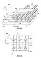
- FIG. 2Ais an illustration of a semiconductor device 100 that includes a plurality of memory cells 102 , each including a thyristor 104 and an associated control gate 106 .
- the plurality of memory cells 102 of the semiconductor device 100may be disposed on a conductive strap 108 overlying an electrically insulative material 150 , which may also be characterized as a dielectric material.
- the electrically insulative material 150is hereinafter referred to as insulative material 150 .
- Each of the thyristors 104may have a general shape of a column or pillar and may include a semiconductor material, such as a crystalline silicon material, a silicon germanium (Si 1-x Ge x ) material, a gallium arsenide (GaAs) material or a gallium nitride (GaN) material.
- the thyristors 104may each include a plurality of vertically superposed, alternately doped regions, such as cathode region 116 , p base region 114 , n base region 112 and anode region 110 .
- the anode region 110may include a highly doped p-type silicon material (i.e., a p+ material).
- the n base region 112may comprise an n-type silicon material.
- the p base region 114may include a p-type silicon material.
- the cathode region 116may include a highly doped semiconductor material (i.e., an n+ material), such as a highly doped silicon germanium material, a highly doped gallium arsenide material or a highly doped gallium nitride material.
- the term “highly doped,” as used herein,means and includes a material having a higher concentration of a dopant than those which are not highly doped. Accordingly, the anode region 110 and the cathode region 116 may, respectively, have an increased dopant concentration in comparison to the p base region 114 and the n base region 112 .
- the thyristors 104have a substantially reduced area in comparison to conventional horizontally aligned thyristors. Accordingly, a footprint of the semiconductor device 100 may be substantially reduced in comparison to conventional T-RAM cells.
- the memory cells 102may be arranged in an array that includes a plurality of rows extending in a first direction X and a plurality of columns extending in a second direction Y.
- the semiconductor device 100 shown in FIG. 2Aincludes three (3) rows and four (4) columns of thyristors 104 .
- the semiconductor device 100may include any number of rows and columns.
- the rows of thyristors 104 aligned in the first direction Xmay be substantially perpendicular to the columns of thyristors 104 aligned in the second direction Y.
- the semiconductor device 100may be disposed on the insulative material 150 overlying a wafer (not shown), which may include a conventional logic device, as will be described in detail.
- the control gates 106may each include a conductive material and may be each be disposed over at least one sidewall of a thyristor 104 .
- a gate dielectric 124may be disposed between the control gates 106 and each of the associated thyristors 104 .
- each of the memory cells 102may include a control gate 106 disposed on the gate dielectric 124 on a single sidewall of the thyristors 104 or may include control gates 106 disposed on opposite sidewalls of the thyristors 104 .
- control gates 106may extend in the second direction Y and may be disposed over at least one of the sidewalls of the thyristors 104 aligned in the columns extending in the second direction Y.
- the control gates 106 or the gate dielectric 124if present, may directly contact the p base region 114 of the thyristors 104 without contacting the n base region 112 or the cathode region 116 flanking the p base region 114 .
- Each of the control gates 106may be operably connected to a voltage source (not shown) for biasing the thyristors 104 of the semiconductor device 100 .
- Each of the conductive straps 108may include amorphous silicon 128 and a conductive material 130 and may be disposed between the insulative material 150 and a plurality of the thyristors 104 .
- the conductive straps 108may function as an electrical interconnect to the cathode regions 116 of one or more of the thyristors 104 of the semiconductor device 100 .
- the conductive straps 108may each extend in the direction X, underlying at least one of the rows.
- the cathode region 116 of each of the thyristors 104 in the rowmay be electrically coupled with an underlying one of the conductive straps 108 .
- the conductive straps 108may be aligned substantially perpendicular to the control gates 106 .
- Each of the conductive straps 108may include an interconnect region 132 that may remain exposed to enable the semiconductor device 100 to be electrically coupled with another device (not shown), such as an underlying conventional logic device.
- Vertical surfaces of the conductive straps 108may be aligned with sidewalls of the thyristors 104 in one of the rows.
- Conductive lines 134may be disposed over a plurality of the memory cells 102 of the semiconductor device 100 .
- each of the conductive lines 134may be disposed over and in contact with the anode regions 110 of each of the memory cells 102 arranged in one of the rows and may, thus, function as an electrical interconnect to each of the anode regions 110 .
- Each of the conductive lines 134may be, for example, disposed above and substantially perpendicular to one of the control gates 106 .
- the control gates 106may be biased using the voltage source such that a depletion base region is created, providing current flow from the cathode region 116 to the anode region 110 of each of the thyristors 104 .
- the conductive lines 134may each function as a data/sense line (i.e., bit line) and, during operation of the semiconductor device 100 , may create a forward bias electrically coupling the memory cells 102 of the semiconductor device 100 .
- the conductive straps 108may function as electrical contacts to the cathode regions 116 of each of the memory cells 102 .
- FIG. 2Bis an electrical diagram of a portion of the semiconductor device 100 shown in FIG. 2A .
- the memory cells 102are disposed in a plurality of rows 118 and columns 120 and each include a thyristor 104 and a control gate 106 .
- Each of the control gates 106is electrically coupled to the thyristors 104 in one of the rows 118 and each of the conductive straps 108 and the conductive lines 134 are electrically coupled to the thyristors 104 in one of the columns 120 .
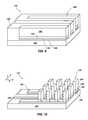
- FIG. 3Ais an illustration of a semiconductor device 200 having substantially the same configuration as the semiconductor device 100 shown in FIG. 2A with the exception of the ordering of the vertically superposed, doped regions of the thyristors 104 .
- each of the thyristors 104may be reversed with respect to those shown in FIG. 2A so that the anode region 110 is disposed on one of the conductive straps 108 , the n base region 112 is disposed over the anode region 110 , the p base region 114 is disposed between the n base region 112 and the cathode region 116 .
- the memory cells 102may be arranged in an array that includes a plurality of rows extending in a first direction X and a plurality of columns extending in a second direction Y, as described with respect to FIG. 2A .
- the control gates 106 of the semiconductor device 200may be disposed along the p base region 114 of the thyristors 104 .
- Each of the control gates 106may be operably connected to a voltage source (not shown) for biasing the memory cells 102 of the semiconductor device 200 .
- a voltagemay be applied to the conductive lines 134 which may function as cathodes while the conductive straps 108 may each function as a data/sense line (i.e., bit line) and may create a forward bias electrically coupling the memory cells 102 of the semiconductor device 200 .
- FIG. 3Bis an electrical diagram of a portion of the semiconductor device 200 shown in FIG. 3A .
- the memory cells 102are disposed in a plurality of rows 118 and columns 120 and each include a thyristor 104 and a control gate 106 .
- Each of the control gates 106is electrically coupled to the thyristors 104 in one of the rows 118 and each of the conductive straps 108 and the conductive lines 134 are electrically coupled to the thyristors 104 in one of the columns 120 .
- FIG. 4is a fragmentary top-down view of a portion of the semiconductor devices 100 and 200 shown in FIGS. 2A though 3 B.
- the control gates 106extend laterally in rows and the conductive lines 134 extend vertically thereover in columns.
- the conductive lines 134overlie a doped region (not shown) comprising a p-type crystalline silicon material.
- the conductive lines 134overlie a doped region (not shown) comprising a an n-type crystalline silicon material.
- Each of the memory cells 102has a cell size of 4F 2 .
- the 4F 2 cell sizeis achieved by providing the conductive strap 108 as a cathode or bit line during operation of the semiconductor device 100 .
- a donor wafer 136may be formed that includes a substrate 138 having a doped material 140 , the conductive material 130 and amorphous silicon 128 formed thereon.
- the substrate 138may include a fabrication substrate, such as a full or partial wafer of semiconductor material (e.g., silicon, silicon germanium, gallium arsenide, indium phosphide, etc.), a full or partial silicon-on-insulator (SOI) type substrate, such as a silicon-on-glass (SOG), silicon-on-ceramic (SOC), or silicon-on-sapphire (SOS) substrate, or any other known, suitable fabrication substrate.
- SOIsilicon-on-insulator
- SOIsilicon-on-insulator
- SOGsilicon-on-glass
- SOCsilicon-on-ceramic
- SOSsilicon-on-sapphire
- the term “wafer”includes conventional wafers as well as other bulk semiconductor substrates.
- the substrate 138may include a crystalline silicon material.
- the substrate 138may be doped or undoped.
- the substrate 138may be doped with a p-type impurity to form a p-type silicon material that may be used to form the semiconductor device 100 shown in FIG. 2A .
- the substrate 138may be doped with an n-type impurity to form an n-type silicon material that may be used to form the semiconductor device 200 shown in FIG. 3A .
- the doped material 140may include a highly doped n-type material that may be used to form the cathode regions 116 of the semiconductor device 100 shown in FIG. 2A or a highly doped p-type material that may be used to form the anode regions 110 of the semiconductor device 200 shown in FIG. 3A , as will be described in further detail.
- the doped material 140may be formed by performing a conventional ion implantation on the substrate 138 .
- the doped material 140may be formed to include a highly doped n-type silicon material (i.e., n+ material) by implanting ions of an n-type impurity, such as arsenic (As), phosphorous (P) or antimony (Sb), into the substrate 138 .
- n+ materiala highly doped n-type silicon material
- the doped material 140 including the n+ materialmay be used to form the cathode regions 116 of the semiconductor device 100 shown in FIG. 2A , as will be described in further detail.
- the doped material 140may be formed to include a highly doped p-type silicon material (i.e., p+ material) by implanting ions of a p-type impurity, such as boron (B), into the substrate 138 .
- the doped material 140 including the p+ materialmay be used to form the anode regions 110 of the semiconductor device 200 shown in FIG. 3A , as will be described in further detail.
- the doped material 140may be formed before or after the conductive material 130 and the amorphous silicon 128 have been formed on the donor wafer 136 .
- the doped material 140may be formed by epitaxially growing or depositing doped silicon germanium, doped gallium arsenide, or doped gallium nitride on the substrate 138 to improve mobility and provide better control over diffusion of dopants in the doped material 140 .
- the conductive material 130may be a low resistivity material including, but not limited to, a phase change material, titanium, titanium silicide, titanium oxide, titanium nitride, tantalum, tantalum silicide, tantalum oxide, tantalum nitride, tungsten, tungsten silicide, tungsten oxide, tungsten nitride, other metals, metal silicide, metal oxide, or metal nitride materials, or combinations thereof, including multiple, different conductive materials.
- the conductive material 130may be formed from titanium nitride because titanium nitride has good adherence or adhesion to many materials, such as the material used as the substrate 138 .
- Titanium nitridealso has a high melting point (about 3000° C.), which makes it unaffected by high processing temperatures. Titanium nitride also makes excellent ohmic contact with other conductive materials. Titanium nitride is also commonly used in semiconductor fabrication and, therefore, may easily be incorporated into conventional fabrication processes.
- the conductive material 130is a titanium-rich titanium nitride, such as metal mode titanium nitride (MMTiN).
- MMTiNmetal mode titanium nitride
- the conductive material 130may also be formed from multiple conductive materials.
- the conductive material 130may be formed from a metal, such as titanium, tungsten or aluminum, with a layer of titanium nitride material formed thereon.
- the thickness of the conductive material 130may be optimized, depending on the material, to provide a low ohmic contact.
- the conductive material 130is titanium nitride, such as MMTiN
- the conductive material 130may have a thickness of from about 10 nm to about 50 nm.
- the conductive material 130may be formed by a deposition technique known in the art, such as, for example, atomic layer deposition (ALD), chemical vapor deposition (CVD), or plasma vapor deposition (PVD).
- the amorphous silicon 128may be formed over the conductive material 130 by a deposition technique known in the art, such as, for example, ALD, CVD, or PVD. In one embodiment, the amorphous silicon 128 may be formed on the conductive material 130 by PVD, followed by chemical-mechanical planarization (CMP). The thickness of the amorphous silicon 128 may be from about 10 nm to about 80 nm.
- the donor wafer 136may also include a transfer region 146 formed by implanting an atomic species into the substrate 138 .
- the atomic speciesmay be hydrogen ions, ions of rare gases, also termed inert or noble gases, or ions of fluorine.
- the atomic speciesmay be implanted into the substrate 138 of the donor wafer 136 to form an implanted zone 148 , represented in FIG. 5 by broken lines.
- the atomic speciesmay be implanted into the substrate 138 before or after the conductive material 130 or the amorphous silicon 128 are formed on the substrate 138 .
- the implanted zone 148may be formed at a desired depth in the substrate 138 , which is dependent on parameters, such as implant dose and energy of the atomic species, as known in the art.
- the depth of the implanted zone 148may be controlled based on a desired thickness of the thyristors 104 shown in FIGS. 2A and 3A .
- the implanted zone 148may include microbubbles or microcavities including the implanted atomic species, which provide a weakened region within the substrate 138 .
- the donor wafer 136may be thermally treated at a temperature above that at which implantation is effected, but below the melting temperature of the conductive material 130 , to effect crystalline rearrangement in the donor wafer 136 and coalescence of the microbubbles or microcavities. As described below, the donor wafer 136 may be cleaved at the implanted zone 148 to form a semiconductor structure 172 ′ shown in FIG. 6 .
- the donor wafer 136may be superposed onto the insulative material 150 overlying an acceptor wafer 152 such that the amorphous silicon 128 of the donor wafer 136 is in contact with the insulative material 150 .
- the insulative material 150may be formed over a bulk substrate 154 using a conventional deposition technique known in the art, such as, for example, ALD, CVD, or PVD.
- the bulk substrate 154may include a silicon substrate.
- An at least partially fabricated conventional logic device, such as a complementary metal-oxide-semiconductor (CMOS) device 156may optionally be formed on the bulk substrate 154 and may be formed by conventional techniques.
- CMOScomplementary metal-oxide-semiconductor
- the CMOS device 156may include an array of field effect transistors (FETs) 158 disposed between source regions 160 and drain base regions 162 in the bulk substrate 154 .
- FETsfield effect transistors
- Each of the FETs 158may include a gate dielectric 163 and a gate electrode 164 disposed between spacers 166 .
- a dielectric material 168may, optionally, be formed between the bulk substrate 154 and the gate electrode 164 of each of the FETs 158 .
- the CMOS device 156may further include a plurality of line interconnects 170 interconnecting the FETs 158 .
- the amorphous silicon 128 of the donor wafer 136may then be bonded to the insulative material 150 of the acceptor wafer 152 by exposure to heat.
- a surface of the amorphous silicon 128 and a surface of the insulative material 150may, optionally, be treated to improve the bond strength therebetween.
- Such treatment techniquesare known in the art and may include, for example, chemical activation, plasma activation or implant activation.
- the surface of the insulative material 150may be treated with a dilute ammonia hydroxide solution or hydrogen fluoride solution.
- the surface of the amorphous silicon 128may also be exposed to a plasma of, for example, argon, to form a plasma-activated surface. Activating at least one of the surface of the amorphous silicon 128 and the surface of the insulative material 150 may increase the kinetics of the subsequent bonding therebetween due to an increased mobility of ionic species (for example, hydrogen) created on the surface of the amorphous silicon 128 and the surface of the insulative material 150 .
- ionic speciesfor example, hydrogen
- the amorphous silicon 128 of the donor wafer 136may be contacted and bonded with the insulative material 150 of the acceptor wafer 152 to form a semiconductor structure 172 ′.
- the amorphous silicon 128may be bonded to the insulative material 150 by, for example, heating the semiconductor structure 172 ′ to a temperature of less than about 600° C., such as from about 300° C. to about 400° C. If the insulative material 150 is formed from silicon dioxide, silicon-oxide bonds may form between the amorphous silicon 128 and the insulative material 150 .
- the temperature to which the semiconductor structure 172 ′ is exposedmay be less than the melting point of the conductive material 130 .
- the amorphous silicon 128 and the insulative material 150may also be bonded without heat, such as at ambient temperature (from about 20° C. to about 25° C.). Pressure may also be applied to the donor wafer 136 and the acceptor wafer 152 to bond the amorphous silicon 128 to the insulative material 150 . Once the donor wafer 136 is bonded to the acceptor wafer 152 , the conductive material 130 from the donor wafer 136 may form a buried conductive material, which is disposed between the insulative material 150 and the substrate 138 .
- the transfer region 146may then be removed from the substrate 138 , to form the semiconductor structure 172 shown in FIG. 7 .
- the transfer region 146may be removed by techniques known in the art, such as by applying a shear force to the implanted zone 148 ( FIG. 6 ) or by applying heat or a jet gas stream at the implanted zone 148 .
- the hydrogen or other ions implanted in implanted zone 148produce a weakened region in the substrate 138 , which is susceptible to cleavage.
- the remaining portion of the substrate 138 ′may have a thickness, for example, of from about 50 nm to about 30 nm (from about 500 ⁇ to about 3000 ⁇ ).
- an exposed surface 176 of the substrate 138 ′may be undesirably rough.
- the exposed surface 176 of the substrate 138 ′may be smoothed to facilitate further processing as described, according to techniques known in the art such as, for example, one or more of grinding, wet etching, and chemical-mechanical polishing (CMP).
- the semiconductor structure 172may be formed by modification of SMART-CUT® layer transfer technology.
- the SMART-CUT® layer transfer technologyis described in detail in, for example, U.S. Pat. No. RE 39,484 to Bruel, U.S. Pat. No. 6,303,468 to Aspar et al., U.S. Pat. No. 6,335,258 to Aspar et al., U.S. Pat. No. 6,756,286 to Moriceau et al., U.S. Pat. No. 6,809,044 to Aspar et al., U.S. Pat. No. 6,946,365 to Aspar et al., and U.S. Patent Application Publication No.
- Exemplary methods for forming the semiconductor structure 172are described in detail in U.S. patent application Ser. No. 12/715,704 filed on even date herewith and titled “SILICON-METAL-ON-INSULATOR STRUCTURES, METHODS OF FORMING SUCH STRUCTURES, AND SEMICONDUCTOR DEVICES INCLUDING SUCH STRUCTURES”. While FIGS. 6 and 7 illustrate one embodiment of a method of forming the semiconductor structure 172 , any of the methods described in U.S. patent application Ser. No. 12/715,704, or other known methods may be utilized to form the semiconductor structure 172 .
- portions of the substrate 138 ′, the doped material 140 , the conductive material 130 and the amorphous silicon 128may be removed to form the conductive straps 108 , each of which may function as a cathode interconnection in the semiconductor device 100 shown in FIG. 2A or as a bit line in the semiconductor device 200 shown in FIG. 3A .
- Forming the semiconductor structure 172 , including the buried conductive material 130 by the bonding and material transfer process described with respect to FIGS. 5 through 7enables formation of the conductive straps 108 , which is not possible using either a conventional silicon wafer or a conventional silicon-on-insulator (SOI) structure.
- SOIsilicon-on-insulator
- the conductive straps 108may be formed by depositing a mask material (not shown) over the substrate 138 ′ and patterning the mask material to form apertures through which surfaces of the substrate 138 ′ are exposed.
- the mask materialmay include, for example, a photoresist material, an oxide material, transparent carbon or amorphous carbon. Methods of forming and patterning the mask material are known in the art and, therefore, are not described in detail herein.
- Portions of the substrate 138 ′, the doped material 140 , the conductive material 130 and the amorphous silicon 128 exposed through the apertures in the mask materialmay be removed to form slots 178 between remaining portions of each of the substrate 138 ′, the doped material 140 , the conductive material 130 and the amorphous silicon 128 . The remaining portions of the mask material may then be removed.
- the slots 178may be formed extending in the first direction X through each of the substrate 138 ′, the doped material 140 , the conductive material 130 and the amorphous silicon 128 . Portions of the substrate 138 ′, the doped material 140 , the conductive material 130 and the amorphous silicon 128 may be removed using, for example, an anisotropic reactive ion (i.e., plasma) etching process, to expose the underlying insulative material 150 .
- an anisotropic reactive ioni.e., plasma
- a reactive ion etching (RIE) processusing oxygen (O 2 ) gas, tetrafluoromethane (CF 4 ) gas and hydrogen bromide (HBr) gas may be performed to selectively remove portions of the doped silicon material selective to the mask material and the insulative material 150 .
- RIEreactive ion etching
- the conductive material 130is formed from titanium nitride or tungsten silicide, a mixture of a bromine-containing gas and a fluorine-containing gas or a mixture of a fluorine-containing gas and a chlorine-containing gas may be used to remove the titanium nitride and the amorphous silicon material selective to the mask material and the insulative material 150 .
- a fill material 180may be formed over the semiconductor structure 172 .
- the fill material 180may include a dielectric material such as an oxide material, a nitride material or a spin-on-glass (SOG) material, and may be deposited using a chemical vapor deposition process.
- a chemical-mechanical polishing (CMP) processmay be used to remove portions thereof so that an upper surface 174 of the semiconductor structure 172 is substantially planar.
- FIG. 10shows the semiconductor structure 172 after portions of the substrate 138 ′ and the doped material 140 ( FIG. 9 ) have been removed to form a plurality of pillars 182 and to expose the interconnect regions 132 of the conductive straps 108 .
- the fill material 180has been omitted for simplicity and clarity of illustration.
- Each of the pillarsincludes a remaining portion of the substrate 138 ′′ and the doped material 140 ′.
- pillars 182may each include an cathode region 116 and a p base region 114 to form one of the thyristors 104 of the semiconductor device 100 shown in FIG. 2A .
- each of the pillars 182may include the anode regions 110 and the n base regions 112 to form the thyristors 104 of the semiconductor device 200 shown in FIG. 3A .
- the pillars 182may be formed by depositing a mask material (not shown) over the semiconductor structure 172 and patterning the mask material to form apertures through which surfaces of the substrate 138 ′ are exposed.
- surfaces of the fill material 180FIG. 9 ) may be exposed through the mask material.
- the mask materialmay include, for example, a photoresist material, an oxide material, transparent carbon or amorphous carbon. Methods of forming and patterning the mask material are known in the art and, therefore, are not described in detail herein.
- Portions of the substrate 138 ′ and the doped material 140 exposed through the apertures in the mask materialmay be removed to form the pillars 182 and to expose the interconnect regions 132 of the conductive straps 108 .
- a reactive ion etching (RIE) processmay be performed to selectively remove portions of the doped crystalline silicon without removing conductive material 130 from the conductive straps 108 .
- RIEreactive ion etching
- Each of the pillars 182may be formed to have an aspect ratio of from about 2:1 to about 20:1 and, more particularly, from about 3:1 to about 10:1.
- the pillars 182 shown in FIG. 10are formed by completely removing the doped material 140 ( FIG.
- the pillars 182may be formed by removing only the substrate 138 ′ ( FIG. 9 ), or a portion thereof, such that at least a portion of the doped material 140 remains over the conductive straps 108 , as shown in broken lines.
- the cathode region 24is formed by conventional doping processes wherein the dopants are implanted from the upper surface of the vertical thyristor 12 to the cathode region 24 .
- Such doping processesoften result in an undesirable concentration or distribution of dopants or impurities and, thus, are not effective for introducing dopants or impurities into substantial depths of material, such as the cathode region 24 of the vertical thyristor 12 shown in FIG. 1A .
- the bonding and material transfer process described with respect to FIGS. 5 through 7enables doping of the substrate 138 , 138 ′ and the doped material 140 prior to material transfer.
- the qualities of the substrate 138 , 138 ′ and the doped material 140are substantially improved. Since the substrate 138 , 138 ′ and the doped material 140 may be doped before forming the pillars 182 , the method of the present invention enables control and optimization of dopant concentration of cathode regions 116 and the p base regions 114 of the semiconductor device 100 shown in FIG. 2A and the anode regions 110 and the n base regions 112 of the semiconductor device 200 shown in FIG. 3A .
- the pillars 182may be formed in an array that includes a plurality of rows in which the pillars 182 are aligned in the first direction X and a plurality of columns in which the pillars 182 are aligned in the second direction Y.
- the substrate 138 ′ and the doped material 140may be removed such that the interconnect regions 132 have a staggered configuration that may be useful in electrically interconnecting the conductive straps 108 with underlying or overlying semiconductor structures (not shown).
- FIGS. 11A through 11Cillustrate an embodiment of a method of forming the control gates 106 on the pillars 182 and are perspective views of the semiconductor structure 172 shown in FIG. 10 after a gate dielectric material 184 and a conductive material 186 have been deposited over the semiconductor device 172 .
- FIG. 11Aillustrates the semiconductor device 172 having the fill material 180 disposed between the pillars 182 .
- a gate dielectric material 184 and a conductive material 186may be conformally formed over the semiconductor structure 172 .
- the gate dielectric material 184may be an oxide material or a nitride material formed using, for example, a chemical vapor deposition process, a thermal oxidation process or a combination thereof.
- the conductive material 186may then be formed over the gate dielectric material 184 .
- the conductive material 186may be formed from titanium nitride, thallium nitride tungsten or aluminum and may be deposited using a chemical vapor deposition process.
- a liner material(not shown), such as a polysilicon material having a thickness of between about 50 ⁇ and 100 ⁇ may be deposited over the conductive material 186 . Referring to FIG.
- 11C anisotropic dry etching processmay be performed to remove portions of the liner and the conductive material 186 to foam spacers (not shown) of the liner material overlying remaining portions of the conductive material 186 .
- a wet etching processusing, for example, ammonium hydroxide (NH 4 OH), hydrogen peroxide (H 2 O 2 ) and deionized water, may be performed to undercut the conductive material 186 to form the control gates 106 shown in FIG. 12 . The spacers may then be removed.
- TMAHtetramethylammonium hydroxide
- the control gates 106 and the gate dielectric 124may be formed using any other technique known in the art.
- the control gates 106are formed on two (2) surfaces of the pillars 182 .
- the control gates 106may also be formed on a single side of the pillars 182 .
- a mask material(not shown) may be deposited over the semiconductor structure 172 and patterned to form a plurality of apertures through which surfaces of the control gates 106 on one side of the pillars 182 are exposed.
- a conventional etching processmay be performed to remove the exposed portion of each of the control gates 106 so that the control gates 106 remains on a single side of the pillars 182 .
- the gate dielectric 124may, optionally, be removed selective to control gates 106 .
- the an upper region of each of the pillars 182may be implanted with a dopant or impurity to form the n base regions 112 of the semiconductor device 100 shown in FIG. 2A , or the p base regions 114 of the semiconductor device 200 shown in FIG. 3A .
- Exposed portions of the pillars 182may be doped using conventional methods, such as an ion implantation process or a high temperature diffusion process.
- the semiconductor device 172may be formed by exposing the semiconductor device 172 to an n-type dopant, such as phosphorous or arsenic, such that an n-type material is formed.
- the p base regions 114 of the thyristors 104 of the semiconductor device 200 shown in FIG. 3Amay be formed by exposing the semiconductor device 172 to a p-type dopant, such as boron or aluminum, such that a p-type material is formed.
- a thin film of a highly doped p-type material or a highly doped n-type materialmay be deposited over exposed surfaces of the pillars 182 and a thermal anneal may be performed during which dopants migrate from the highly doped p-type material or the highly doped n-type material into the pillars 182 producing the desired doped material (i.e., the n base regions 112 shown in FIG. 2A or the p base regions 114 shown in FIG. 3A ).
- an upper region of each of the pillars 182may be implanted with a dopant or impurity to form the anode regions 110 of the semiconductor device 100 shown in FIG. 2A , or the cathode regions 116 of the semiconductor device 200 shown in FIG. 3A .
- Exposed portions of the pillars 182may be doped using conventional methods, as described with respect to FIG. 12 .
- the cathode regions 116 of the semiconductor device 200 shown in FIG. 3Amay be formed by exposing the semiconductor device 172 to an n-type dopant or by depositing a highly doped n-type material on exposed surfaces of the pillars 182 and performing a thermal anneal, such that the highly doped p-type material is formed.
- a donor wafer 136 ′may be formed having a structure similar to the donor wafer 136 shown in FIG. 5 , and may additionally include a first material 142 and a second material 144 .
- the first material 142 and the second material 144may be formed by a conventional doping process, which may be performed by exposing either a first major surface 188 or a second major surface 190 of the donor wafer 136 ′ to a dopant or impurity.
- the substrate 138may include a highly doped n-type material
- the first material 142may include a p-type material
- the second material 144may include an n-type material
- the doped material 140may include a highly doped p-type material such that, upon formation of the pillars 182 as described with respect to FIG. 10 , the thyristors 104 of the semiconductor device 100 shown in FIG. 2A are formed.
- the substrate 138may include a highly doped p-type material
- the first material 142may include an n-type material
- the second material 144may include a p-type material
- the doped material 140may include a highly doped n-type material such that, upon formation of the pillars 182 as described with respect to FIG. 10 , the thyristors 104 of the semiconductor device 200 shown in FIG. 3A are formed. Doping the substrate 138 prior to the bonding and material transfer process described with respect to FIGS. 5 through 7 thus enables the concentration and distribution of dopants therein to be controlled and optimized.
- a voltagemay be applied to the control gate 106 , causing an electrical current to flow from the cathode region 116 to the anode region 110 of the thyristors 104 shown in FIGS. 2A through 3B .
- overlap between the control gates 106 and the associated p base regions 114 of the thyristors 104may occur. Such overlap may create capacitance and increase leakage current during operation of the completed device, thus, limiting the density of the array. Accordingly, the p base regions 114 and the associated control gates 106 may be formed to minimize overlap of the control gates 106 with the cathode regions 116 and the n base regions 112 flanking the p base regions 114 .
- portions of the control gates 106 that extend above the p base regions 114may be removing using, for example, a conventional plasma etching process so that the control gates 106 do not extend beyond interfaces between the p base regions 114 and each of the cathode regions 116 and n base regions 112 .
- the conductive lines 134may be formed over and in contact with the thyristors 104 to form the semiconductor devices 100 and 200 .
- the conductive lines 134may be formed by depositing a conductive material and patterning the conductive material to form conductive lines extending in the first direction X, substantially perpendicular to the control gates 106 .
- the conductive lines 134may be formed using a conventional damascene or subtractive process.
- a conductive material(not shown) may be formed over the semiconductor structure 172 ( FIG. 12 ) and portions thereof may be removed through apertures in a photoresist material to define the conductive lines 134 .
- the conductive lines 134may be formed using a conventional lithographic process.
- a sacrificial dielectric material(not shown) may be deposited over the semiconductor structure 172 and a pattern of trenches (not shown) may be formed therein using a conventional lithographic process. Each of the trenches may be formed in locations at the conductive lines 134 are to be formed.
- a conductive materialmay be deposited over the semiconductor structure 172 to fill the trenches and a chemical-mechanical polishing process may be used to remove a portion of the conductive material overlying the dielectric material to form the conductive lines 134 .
- the methods shown in FIGS. 5-13may be repeated to form a multi-level semiconductor device including a plurality of vertically-stacked semiconductor devices, memory or logic and having increased memory density.
- the conductive lines 134function as data lines (i.e., bit lines) during operation of the semiconductor device 100 shown in FIGS. 2A and 2B and as cathodes during operation of the semiconductor device 200 shown in FIGS. 3A and 3B .
- FIG. 15illustrates a simplified block diagram of an electronic system 300 implemented according to one or more embodiments described herein.
- the electronic system 300includes at least one input device 302 , at least one output device 304 , a memory access device, such as one or more processors 306 , and one or more memory devices 308 .
- the memory devices 308include at least one semiconductor memory 310 incorporating at least one embodiment of the devices or methods described herein.
- the electronic system 300may be part of a number of computing, processing, and consumer products. As non-limiting examples, some of these products may include personal computers, handheld devices, cameras, phones, wireless devices, displays, chip sets, set top boxes, games, and vehicles.
- the present inventionincludes memory cells that include a conductive strap disposed over a substrate, a thyristor disposed on the conductive strap and including a plurality of alternately doped, vertically superposed semiconductor regions and a control gate disposed on one of the plurality of alternately doped, vertically superposed semiconductor regions of the thyristor.
- the conductive strap disposed over a substratemay include a conductive material overlying amorphous silicon. At least two sidewalls of the conductive strap may be aligned with sidewalls of the thyristor.
- the thyristormay include an cathode region, a p base region, an n base region, and a anode region being vertically superposed over one another.
- the control gatemay be disposed on exposed sidewalls of the n-type silicon.
- the control gatemay be operably coupled to a voltage source.
- the memory cellmay have a cell size of 4F 2 .
- the present inventionincludes semiconductor devices that include at least one conductive strap, a plurality of memory cells disposed on the at least one conductive strap, and a data line electrically coupled with at least a portion of the plurality of memory cells.
- Each of the plurality of memory cellsmay include a thyristor comprising a plurality of alternately doped, vertically superposed semiconductor regions and a control gate associated with the thyristor.
- Each of the memory cells of the pluralitymay have a cell size of 4F 2 .
- the at least one conductive strapmay be disposed on an electrically insulative material overlying a logic device formed on a wafer.
- the thyristorincludes four doped regions of alternating dopant types forming three semiconductor junctions.
- the plurality of memory cellsmay be aligned in a plurality of rows extending in a first direction and aligned in a plurality of columns extending in a second direction perpendicular to the first direction to form an array.
- the thyristor of each of the plurality of memory cellscomprises a highly doped n-type region disposed on the at least one conductive strap, a p-type region disposed on the highly doped n-type region, an n-type region disposed on the p-type region, and an a highly doped p-type region disposed on the n-type region.
- the present inventionincludes a memory array that includes an array of memory cells including a plurality of thyristors substantially aligned in a plurality of rows in a first direction and in a plurality of columns in a second direction perpendicular to the first direction, each of the plurality of thyristors comprising a plurality of vertically superposed, alternately doped semiconductor regions, and at least one control gate electrically coupled with one of the plurality of vertically superposed, alternately doped semiconductor regions of each of the plurality of thyristors in at least one of the plurality of columns.
- the memory cellfurther includes a plurality of conductive straps, each electrically coupled with each of the plurality of thyristors aligned in one of the plurality of rows.
- the at least one control gatemay be disposed on at least one sidewall of each of the plurality of thyristors aligned in one of the plurality of columns.
- Each of the plurality of thyristors in one of the plurality of rows of the array of memory cellsmay be disposed on one of the plurality of conductive straps.
- the plurality of conductive linesmay be disposed over and aligned with the thyristors aligned in one of the plurality of rows.
- the memory arraymay further include at least one logic device electrically coupled to the at least one of the plurality of conductive straps.
- the present inventionincludes a method of forming a semiconductor device.
- the methodincludes forming a semiconductor structure comprising amorphous silicon overlying an electrically insulative material, a conductive material overlying the amorphous silicon, a doped material overlying the conductive material and a doped crystalline silicon overlying the doped material, removing portions of each of the doped crystalline silicon, the doped material, the conductive material and the amorphous silicon to form a plurality of channels exposing the electrically insulative material, removing portions of the doped crystalline silicon and the doped material to form a plurality of pillars, each including a first doped region and a second doped region oppositely doped with respect to the first doped region, forming a control gate on at least one surface of each of the plurality of pillars, exposing the plurality of pillars to a first dopant to form a third doped region, oppositely doped with respect to the second doped region and exposing the
- the methodsmay further include forming a conductive line over and in contact with the fourth doped region of each of the plurality of pillars.
- the semiconductor structuremay be formed by forming a donor wafer comprising the amorphous silicon overlying the conductive material, the conductive material overlying the doped material disposed on a crystalline silicon wafer, implanting ions a predetermined depth into the crystalline silicon wafer, attaching the amorphous silicon of the donor wafer to the electrically insulative material on an acceptor wafer and separating a portion of the donor wafer to leave a portion of the crystalline silicon wafer, the doped material, the conductive material, and the amorphous silicon overlying a surface of the electrically insulative material of the acceptor wafer.
- the semiconductor structuremay include a logic device formed on a wafer underlying the electrically insulative material.
- the present inventionincludes a system including at least memory access device and at least one semiconductor device operably coupled to the at least one memory access device.
- the at least one semiconductor devicemay include at least one conductive strap, a plurality of memory cells disposed on the at least one conductive strap and a data line electrically coupled with at least a portion of the plurality of memory cells.
- Each of the plurality of memory cellsmay include a thyristor and a control gate associated with the thyristor.
- the thyristorsmay each include a plurality of vertically superposed, alternately doped semiconductor regions.
- Each of the plurality of memory cells of the systemmay have a cell size of 4F 2 .
Landscapes
- Engineering & Computer Science (AREA)
- Manufacturing & Machinery (AREA)
- Microelectronics & Electronic Packaging (AREA)
- General Physics & Mathematics (AREA)
- Condensed Matter Physics & Semiconductors (AREA)
- Computer Hardware Design (AREA)
- Physics & Mathematics (AREA)
- Power Engineering (AREA)
- Chemical & Material Sciences (AREA)
- Composite Materials (AREA)
- Chemical Kinetics & Catalysis (AREA)
- General Chemical & Material Sciences (AREA)
- Semiconductor Memories (AREA)
- Thyristors (AREA)
Abstract
Description
Claims (24)
Priority Applications (13)
| Application Number | Priority Date | Filing Date | Title |
|---|---|---|---|
| US12/715,743US9646869B2 (en) | 2010-03-02 | 2010-03-02 | Semiconductor devices including a diode structure over a conductive strap and methods of forming such semiconductor devices |
| US12/715,889US8288795B2 (en) | 2010-03-02 | 2010-03-02 | Thyristor based memory cells, devices and systems including the same and methods for forming the same |
| SG2012062253ASG183451A1 (en) | 2010-03-02 | 2011-02-10 | Thyristor-based memory cells, devices and systems including the same and methods for forming the same |
| PCT/US2011/024376WO2011109147A2 (en) | 2010-03-02 | 2011-02-10 | Thyristor-based memory cells, devices and systems including the same and methods for forming the same |
| KR20127025117AKR101480211B1 (en) | 2010-03-02 | 2011-02-10 | Thyristor-based memory cells, devices and systems including the same and methods for forming the same |
| CN201180011628.6ACN102782848B (en) | 2010-03-02 | 2011-02-10 | Based on thyristor memory cell, comprise its Apparatus and system and for the formation of its method |
| JP2012556082AJP5578454B2 (en) | 2010-03-02 | 2011-02-10 | Thyristor-based memory cells, devices and systems including them, and methods of forming them |
| TW100106775ATWI482278B (en) | 2010-03-02 | 2011-03-01 | Memory unit based on thyristor, device and system therewith and method for forming same |
| US13/610,034US8524543B2 (en) | 2010-03-02 | 2012-09-11 | Thyristor-based memory cells, devices and systems including the same and methods for forming the same |
| US13/965,463US8980699B2 (en) | 2010-03-02 | 2013-08-13 | Thyristor-based memory cells, devices and systems including the same and methods for forming the same |
| US14/642,866US9343462B2 (en) | 2010-03-02 | 2015-03-10 | Thyristor-based memory cells, devices and systems including the same and methods for forming the same |
| US15/464,060US10325926B2 (en) | 2010-03-02 | 2017-03-20 | Semiconductor-metal-on-insulator structures, methods of forming such structures, and semiconductor devices including such structures |
| US15/481,301US10157769B2 (en) | 2010-03-02 | 2017-04-06 | Semiconductor devices including a diode structure over a conductive strap and methods of forming such semiconductor devices |
Applications Claiming Priority (1)
| Application Number | Priority Date | Filing Date | Title |
|---|---|---|---|
| US12/715,889US8288795B2 (en) | 2010-03-02 | 2010-03-02 | Thyristor based memory cells, devices and systems including the same and methods for forming the same |
Related Child Applications (1)
| Application Number | Title | Priority Date | Filing Date |
|---|---|---|---|
| US13/610,034DivisionUS8524543B2 (en) | 2010-03-02 | 2012-09-11 | Thyristor-based memory cells, devices and systems including the same and methods for forming the same |
Publications (2)
| Publication Number | Publication Date |
|---|---|
| US20110215371A1 US20110215371A1 (en) | 2011-09-08 |
| US8288795B2true US8288795B2 (en) | 2012-10-16 |
Family
ID=44530552
Family Applications (4)
| Application Number | Title | Priority Date | Filing Date |
|---|---|---|---|
| US12/715,889Expired - Fee RelatedUS8288795B2 (en) | 2010-03-02 | 2010-03-02 | Thyristor based memory cells, devices and systems including the same and methods for forming the same |
| US13/610,034Expired - Fee RelatedUS8524543B2 (en) | 2010-03-02 | 2012-09-11 | Thyristor-based memory cells, devices and systems including the same and methods for forming the same |
| US13/965,463ActiveUS8980699B2 (en) | 2010-03-02 | 2013-08-13 | Thyristor-based memory cells, devices and systems including the same and methods for forming the same |
| US14/642,866Expired - Fee RelatedUS9343462B2 (en) | 2010-03-02 | 2015-03-10 | Thyristor-based memory cells, devices and systems including the same and methods for forming the same |
Family Applications After (3)
| Application Number | Title | Priority Date | Filing Date |
|---|---|---|---|
| US13/610,034Expired - Fee RelatedUS8524543B2 (en) | 2010-03-02 | 2012-09-11 | Thyristor-based memory cells, devices and systems including the same and methods for forming the same |
| US13/965,463ActiveUS8980699B2 (en) | 2010-03-02 | 2013-08-13 | Thyristor-based memory cells, devices and systems including the same and methods for forming the same |
| US14/642,866Expired - Fee RelatedUS9343462B2 (en) | 2010-03-02 | 2015-03-10 | Thyristor-based memory cells, devices and systems including the same and methods for forming the same |
Country Status (7)
| Country | Link |
|---|---|
| US (4) | US8288795B2 (en) |
| JP (1) | JP5578454B2 (en) |
| KR (1) | KR101480211B1 (en) |
| CN (1) | CN102782848B (en) |
| SG (1) | SG183451A1 (en) |
| TW (1) | TWI482278B (en) |
| WO (1) | WO2011109147A2 (en) |
Cited By (9)
| Publication number | Priority date | Publication date | Assignee | Title |
|---|---|---|---|---|
| US20130001682A1 (en)* | 2011-07-01 | 2013-01-03 | Micron Technology, Inc. | Semiconductor structures including bodies of semiconductor material, devices including such structures and related methods |
| US8576607B1 (en)* | 2010-07-02 | 2013-11-05 | Farid Nemati | Hybrid memory cell array and operations thereof |
| US9209187B1 (en)* | 2014-08-18 | 2015-12-08 | Micron Technology, Inc. | Methods of forming an array of gated devices |
| US9224738B1 (en) | 2014-08-18 | 2015-12-29 | Micron Technology, Inc. | Methods of forming an array of gated devices |
| US9673054B2 (en) | 2014-08-18 | 2017-06-06 | Micron Technology, Inc. | Array of gated devices and methods of forming an array of gated devices |
| US20190013317A1 (en)* | 2017-07-10 | 2019-01-10 | Tc Lab, Inc. | High-Density Volatile Random Access Memory Cell Array and Methods of Fabrication |
| US10388656B2 (en) | 2017-03-24 | 2019-08-20 | United Microelectronics Corp. | Semiconductor device having thyristor and metal-oxide semiconductor transistor |
| US10468414B2 (en) | 2017-12-28 | 2019-11-05 | Samsung Electronics Co., Ltd. | Semiconductor memory devices |
| US11711918B2 (en) | 2020-04-28 | 2023-07-25 | Samsung Electronics Co., Ltd. | Semiconductor memory device and method for fabricating thereof |
Families Citing this family (44)
| Publication number | Priority date | Publication date | Assignee | Title |
|---|---|---|---|---|
| DE102006012738A1 (en) | 2006-03-17 | 2007-09-20 | Infineon Technologies Ag | Benefits of a composite board with semiconductor chips and plastic housing composition as well as methods and molding for the production thereof |
| JP5524547B2 (en)* | 2009-09-14 | 2014-06-18 | ユニサンティス エレクトロニクス シンガポール プライベート リミテッド | Semiconductor memory device |
| US8288795B2 (en) | 2010-03-02 | 2012-10-16 | Micron Technology, Inc. | Thyristor based memory cells, devices and systems including the same and methods for forming the same |
| US9608119B2 (en) | 2010-03-02 | 2017-03-28 | Micron Technology, Inc. | Semiconductor-metal-on-insulator structures, methods of forming such structures, and semiconductor devices including such structures |
| US9646869B2 (en)* | 2010-03-02 | 2017-05-09 | Micron Technology, Inc. | Semiconductor devices including a diode structure over a conductive strap and methods of forming such semiconductor devices |
| US8513722B2 (en) | 2010-03-02 | 2013-08-20 | Micron Technology, Inc. | Floating body cell structures, devices including same, and methods for forming same |
| US8507966B2 (en) | 2010-03-02 | 2013-08-13 | Micron Technology, Inc. | Semiconductor cells, arrays, devices and systems having a buried conductive line and methods for forming the same |
| US20110227173A1 (en)* | 2010-03-17 | 2011-09-22 | Honeywell International Inc. | Mems sensor with integrated asic packaging |
| US8598621B2 (en) | 2011-02-11 | 2013-12-03 | Micron Technology, Inc. | Memory cells, memory arrays, methods of forming memory cells, and methods of forming a shared doped semiconductor region of a vertically oriented thyristor and a vertically oriented access transistor |
| US8952418B2 (en) | 2011-03-01 | 2015-02-10 | Micron Technology, Inc. | Gated bipolar junction transistors |
| US8519431B2 (en) | 2011-03-08 | 2013-08-27 | Micron Technology, Inc. | Thyristors |
| US8772848B2 (en) | 2011-07-26 | 2014-07-08 | Micron Technology, Inc. | Circuit structures, memory circuitry, and methods |
| US9252148B2 (en)* | 2014-01-22 | 2016-02-02 | Micron Technology, Inc. | Methods and apparatuses with vertical strings of memory cells and support circuitry |
| KR102203459B1 (en) | 2014-08-11 | 2021-01-15 | 삼성전자주식회사 | Semiconductor device |
| US20160093624A1 (en) | 2014-09-25 | 2016-03-31 | Kilopass Technology, Inc. | Thyristor Volatile Random Access Memory and Methods of Manufacture |
| US9741413B2 (en) | 2014-09-25 | 2017-08-22 | Kilopass Technology, Inc. | Methods of reading six-transistor cross-coupled thyristor-based SRAM memory cells |
| US9449669B2 (en) | 2014-09-25 | 2016-09-20 | Kilopass Technology, Inc. | Cross-coupled thyristor SRAM circuits and methods of operation |
| US9613968B2 (en) | 2014-09-25 | 2017-04-04 | Kilopass Technology, Inc. | Cross-coupled thyristor SRAM semiconductor structures and methods of fabrication |
| US9530482B2 (en) | 2014-09-25 | 2016-12-27 | Kilopass Technology, Inc. | Methods of retaining and refreshing data in a thyristor random access memory |
| US9564441B2 (en) | 2014-09-25 | 2017-02-07 | Kilopass Technology, Inc. | Two-transistor SRAM semiconductor structure and methods of fabrication |
| US9564199B2 (en) | 2014-09-25 | 2017-02-07 | Kilopass Technology, Inc. | Methods of reading and writing data in a thyristor random access memory |
| KR102310081B1 (en) | 2015-06-08 | 2021-10-12 | 삼성전자주식회사 | Methods of manufacturing semiconductor devices |
| EP3203517A1 (en)* | 2016-02-08 | 2017-08-09 | Kilopass Technology, Inc. | Methods and systems for reducing electrical disturb effects between thyristor memory cells using heterostructured cathodes |
| KR101804666B1 (en)* | 2016-04-06 | 2017-12-05 | 고려대학교 산학협력단 | Semiconductor memory device with vertical semiconductor column |
| KR101835231B1 (en)* | 2016-09-26 | 2018-03-08 | 고려대학교 산학협력단 | Semiconductor Devices |
| US20180102161A1 (en)* | 2016-10-07 | 2018-04-12 | Kilopass Technology, Inc. | Vertical Thyristor Memory Array and Memory Array Tile Therefor |
| US10497712B2 (en) | 2017-03-16 | 2019-12-03 | Toshiba Memory Corporation | Semiconductor memory |
| TWI648825B (en)* | 2017-03-16 | 2019-01-21 | 日商東芝記憶體股份有限公司 | Semiconductor memory |
| US20210013208A1 (en)* | 2017-09-14 | 2021-01-14 | Intel Corporation | Gated thyristors |
| WO2019055009A1 (en)* | 2017-09-14 | 2019-03-21 | Intel Corporation | THYRISTORS |
| US10811602B2 (en)* | 2017-12-08 | 2020-10-20 | Macronix International Co., Ltd. | Tungsten oxide RRAM with barrier free structure |
| US10748903B2 (en)* | 2018-04-19 | 2020-08-18 | Tc Lab, Inc. | Multi-layer random access memory and methods of manufacture |
| KR102304793B1 (en) | 2018-11-08 | 2021-09-27 | 한양대학교 산학협력단 | Manufacturing method of two-terminal thyristor memory device |
| KR102720240B1 (en) | 2018-12-18 | 2024-10-21 | 에스케이하이닉스 주식회사 | semiconductor device having 3-dimensional structure and method of fabricating the same |
| KR102756199B1 (en) | 2019-12-16 | 2025-01-20 | 삼성전자주식회사 | Semiconductor memory device and method for manufacturing the same |
| KR102757541B1 (en) | 2019-12-24 | 2025-01-20 | 삼성전자주식회사 | A vertical memory device and method of manufacturing the same |
| KR102832000B1 (en)* | 2020-01-20 | 2025-07-10 | 삼성전자주식회사 | Semiconductor memory device |
| KR102797253B1 (en) | 2020-05-18 | 2025-04-18 | 삼성전자주식회사 | Semiconductor devices including a semiconductor pattern |
| KR102731055B1 (en) | 2020-09-11 | 2024-11-15 | 삼성전자주식회사 | Semiconductor memory devices |
| KR102784724B1 (en) | 2020-10-07 | 2025-03-21 | 삼성전자주식회사 | Semiconductor memory devices |
| KR20220055513A (en) | 2020-10-26 | 2022-05-04 | 삼성전자주식회사 | Semiconductor memory device |
| KR20220120006A (en)* | 2021-02-22 | 2022-08-30 | 에스케이하이닉스 주식회사 | Memory cell and semiconductor memory dedvice with the same |
| US11810901B2 (en)* | 2021-06-10 | 2023-11-07 | Micron Technology, Inc. | Microelectronic devices, related memory devices and electronic systems, and methods of forming microelectronic devices |
| US11848309B2 (en) | 2021-06-10 | 2023-12-19 | Micron Technology, Inc. | Microelectronic devices, related electronic systems, and methods of forming microelectronic devices |
Citations (81)
| Publication number | Priority date | Publication date | Assignee | Title |
|---|---|---|---|---|
| US5102821A (en) | 1990-12-20 | 1992-04-07 | Texas Instruments Incorporated | SOI/semiconductor heterostructure fabrication by wafer bonding of polysilicon to titanium |
| US5260233A (en) | 1992-11-06 | 1993-11-09 | International Business Machines Corporation | Semiconductor device and wafer structure having a planar buried interconnect by wafer bonding |
| JPH06104446A (en) | 1992-09-22 | 1994-04-15 | Toshiba Corp | Semiconductor device |
| US5563084A (en) | 1994-09-22 | 1996-10-08 | Fraunhofer-Gesellschaft zur F orderung der angewandten Forschung e.V. | Method of making a three-dimensional integrated circuit |
| US6137128A (en) | 1998-06-09 | 2000-10-24 | International Business Machines Corporation | Self-isolated and self-aligned 4F-square vertical fet-trench dram cells |
| US6191476B1 (en) | 1992-10-21 | 2001-02-20 | Seiko Instruments Inc. | Semiconductor device |
| US6229161B1 (en)* | 1998-06-05 | 2001-05-08 | Stanford University | Semiconductor capacitively-coupled NDR device and its applications in high-density high-speed memories and in power switches |
| US20010002062A1 (en) | 1998-05-13 | 2001-05-31 | Noble Wendell P. | High density SRAM cell with latched vertical transistors |
| US6255731B1 (en) | 1997-07-30 | 2001-07-03 | Canon Kabushiki Kaisha | SOI bonding structure |
| US20010024841A1 (en) | 1998-05-13 | 2001-09-27 | Noble Wendell P. | High density vertical sram cell using bipolar latchup induced by gated diode breakdown |
| US6303468B1 (en) | 1997-08-12 | 2001-10-16 | Commissariat A L'energie Atomique | Method for making a thin film of solid material |
| US6335258B1 (en) | 1996-11-05 | 2002-01-01 | Commissariat A L'energie Atomique | Method for making a thin film on a support and resulting structure including an additional thinning stage before heat treatment causes micro-cavities to separate substrate element |
| US6355501B1 (en) | 2000-09-21 | 2002-03-12 | International Business Machines Corporation | Three-dimensional chip stacking assembly |
| US6355520B1 (en) | 1999-08-16 | 2002-03-12 | Infineon Technologies Ag | Method for fabricating 4F2 memory cells with improved gate conductor structure |
| US6365488B1 (en) | 1998-03-05 | 2002-04-02 | Industrial Technology Research Institute | Method of manufacturing SOI wafer with buried layer |
| US20020070454A1 (en) | 2000-11-30 | 2002-06-13 | Seiko Epson Corporation | SOI substrate, element substrate, semiconductor device, electro-optical apparatus, electronic equipment, method of manufacturing the SOI substrate, method of manufacturing the element substrate, and method of manufacturing the electro-optical apparatus |
| US6492662B2 (en) | 2001-04-16 | 2002-12-10 | Ibm Corporation | T-RAM structure having dual vertical devices and method for fabricating the same |
| US6559471B2 (en) | 2000-12-08 | 2003-05-06 | Motorola, Inc. | Quantum well infrared photodetector and method for fabricating same |
| US6600173B2 (en) | 2000-08-30 | 2003-07-29 | Cornell Research Foundation, Inc. | Low temperature semiconductor layering and three-dimensional electronic circuits using the layering |
| US6713791B2 (en) | 2001-01-26 | 2004-03-30 | Ibm Corporation | T-RAM array having a planar cell structure and method for fabricating the same |
| US6744094B2 (en) | 2001-08-24 | 2004-06-01 | Micron Technology Inc. | Floating gate transistor with horizontal gate layers stacked next to vertical body |
| US6756286B1 (en) | 1997-12-30 | 2004-06-29 | Commissariat A L'energie Atomique | Method for transferring a thin film comprising a step of generating inclusions |
| US6809044B1 (en) | 1999-06-30 | 2004-10-26 | Commissariat A L'energie Atomique | Method for making a thin film using pressurization |
| US20040214379A1 (en) | 2000-08-14 | 2004-10-28 | Matrix Semiconductor, Inc. | Rail stack array of charge storage devices and method of making same |
| US20050001232A1 (en) | 2003-07-02 | 2005-01-06 | Micron Technology, Inc. | High-performance one-transistor memory cell |
| US6888199B2 (en) | 2003-10-07 | 2005-05-03 | International Business Machines Corporation | High-density split-gate FinFET |
| US6906354B2 (en) | 2001-06-13 | 2005-06-14 | International Business Machines Corporation | T-RAM cell having a buried vertical thyristor and a pseudo-TFT transfer gate and method for fabricating the same |
| US6946365B2 (en) | 2000-12-08 | 2005-09-20 | Commissariat A L'energie Atomique | Method for producing a thin film comprising introduction of gaseous species |
| US6953953B1 (en) | 2002-10-01 | 2005-10-11 | T-Ram, Inc. | Deep trench isolation for thyristor-based semiconductor device |
| US6995456B2 (en) | 2004-03-12 | 2006-02-07 | International Business Machines Corporation | High-performance CMOS SOI devices on hybrid crystal-oriented substrates |
| US7029956B2 (en) | 2001-04-30 | 2006-04-18 | International Business Machines Corp. | Memory system capable of operating at high temperatures and method for fabricating the same |
| US20060099776A1 (en) | 2004-11-09 | 2006-05-11 | Frederic Dupont | Methods for fabricating compound material wafers |
| US7052941B2 (en) | 2003-06-24 | 2006-05-30 | Sang-Yun Lee | Method for making a three-dimensional integrated circuit structure |
| US20060125011A1 (en) | 2004-03-31 | 2006-06-15 | Chang Peter L | Memory with split gate devices and method of fabrication |
| US7075146B2 (en) | 2004-02-24 | 2006-07-11 | Micron Technology, Inc. | 4F2 EEPROM NROM memory arrays with vertical devices |
| US7120046B1 (en) | 2005-05-13 | 2006-10-10 | Micron Technology, Inc. | Memory array with surrounding gate access transistors and capacitors with global and staggered local bit lines |
| US20060227601A1 (en) | 2004-08-24 | 2006-10-12 | Micron Technology, Inc. | Memory cell with trenched gated thyristor |
| US7157771B2 (en) | 2004-01-30 | 2007-01-02 | Micron Technology, Inc. | Vertical device 4F2 EEPROM memory |
| US20070023805A1 (en) | 2005-07-26 | 2007-02-01 | Wells David H | Reverse construction memory cell |
| USRE39484E1 (en) | 1991-09-18 | 2007-02-06 | Commissariat A L'energie Atomique | Process for the production of thin semiconductor material films |
| US20070045709A1 (en) | 2005-08-29 | 2007-03-01 | Taiwan Semiconductor Manufacturing Co., Ltd. | Vertical flash memory |
| US7268373B1 (en) | 2003-11-12 | 2007-09-11 | T-Ram Semiconductor, Inc. | Thyristor-based memory and its method of operation |
| US7271052B1 (en) | 2004-09-02 | 2007-09-18 | Micron Technology, Inc. | Long retention time single transistor vertical memory gain cell |
| US7279740B2 (en) | 2005-05-12 | 2007-10-09 | Micron Technology, Inc. | Band-engineered multi-gated non-volatile memory device with enhanced attributes |
| US20070252175A1 (en) | 2006-03-29 | 2007-11-01 | Micron Technology, Inc. | Floating body transistor constructions, semiconductor constructions, and methods of forming semiconductor constructions |
| US20070264771A1 (en) | 2006-05-11 | 2007-11-15 | Venkatesan Ananthan | Dual work function recessed access device and methods of forming |
| US7323380B2 (en) | 2002-08-29 | 2008-01-29 | Micron Technology, Inc. | Single transistor vertical memory gain cell |
| US7326969B1 (en) | 2004-12-02 | 2008-02-05 | T-Ram Semiconductor, Inc. | Semiconductor device incorporating thyristor-based memory and strained silicon |
| US7358120B2 (en) | 2005-09-12 | 2008-04-15 | International Business Machines Corporation | Silicon-on-insulator (SOI) read only memory (ROM) array and method of making a SOI ROM |
| US7359229B2 (en) | 2003-05-13 | 2008-04-15 | Innovative Silicon S.A. | Semiconductor memory device and method of operating same |
| US7368352B2 (en) | 2005-10-12 | 2008-05-06 | Samsung Electronics Co., Ltd. | Semiconductor devices having transistors with vertical channels and method of fabricating the same |
| US20080124867A1 (en) | 2006-09-14 | 2008-05-29 | Micron Technology, Inc. | Methods of forming vertical transistors |
| US20080128802A1 (en) | 2005-03-31 | 2008-06-05 | Zong-Liang Huo | Single transistor floating body dram cell having recess channel transistor structure |
| US7415690B2 (en) | 2004-05-19 | 2008-08-19 | Altera Corporation | Apparatus and methods for multi-gate silicon-on-insulator transistors |
| US20080211023A1 (en) | 2007-01-17 | 2008-09-04 | Kabushiki Kaisha Toshiba | Semiconductor memory device and manufacturing method of semiconductor memory device |
| US20080237776A1 (en) | 2004-08-30 | 2008-10-02 | Abbott Todd R | DRAM layout with vertical FETs and method of formation |
| US7456439B1 (en) | 2001-03-22 | 2008-11-25 | T-Ram Semiconductor, Inc. | Vertical thyristor-based memory with trench isolation and its method of fabrication |
| US20090003025A1 (en) | 2007-06-26 | 2009-01-01 | Nima Mokhlesi | Dual bit line metal layers for non-volatile memory |
| US20090010056A1 (en) | 2002-11-20 | 2009-01-08 | The Regents Of The University Of California | Method and apparatus for capacitorless double-gate storage |
| US7476939B2 (en) | 2004-11-04 | 2009-01-13 | Innovative Silicon Isi Sa | Memory cell having an electrically floating body transistor and programming technique therefor |
| US20090022003A1 (en) | 2007-07-20 | 2009-01-22 | Song Ki-Whan | Memory cell structures, memory arrays, memory devices, memory controllers, and memory systems, and methods of manufacturing and operating the same |
| US7488627B1 (en) | 2003-11-12 | 2009-02-10 | T-Ram Semiconductor, Inc. | Thyristor-based memory and its method of operation |
| US20090072341A1 (en) | 2007-09-19 | 2009-03-19 | Micron Technology, Inc. | Buried low-resistance metal word lines for cross-point variable-resistance material memories |
| US20090079030A1 (en) | 2007-09-26 | 2009-03-26 | International Business Machines Corporation | Forming SOI Trench Memory with Single-Sided Buried Strap |
| US7518182B2 (en) | 2004-07-20 | 2009-04-14 | Micron Technology, Inc. | DRAM layout with vertical FETs and method of formation |
| US20090108351A1 (en) | 2007-10-26 | 2009-04-30 | International Business Machines Corporation | Finfet memory device with dual separate gates and method of operation |
| US7538000B2 (en) | 2005-07-28 | 2009-05-26 | Freescale Semiconductor, Inc. | Method of forming double gate transistors having varying gate dielectric thicknesses |
| US20090170261A1 (en) | 2007-12-28 | 2009-07-02 | Hynix Semiconductor Inc. | Method for manufacturing semiconductor device having 4f2 transistor |
| US20090173984A1 (en) | 2008-01-08 | 2009-07-09 | Qimonda Ag | Integrated circuit and method of manufacturing an integrated circuit |
| US20090200536A1 (en) | 2004-06-30 | 2009-08-13 | Koninklijke Philips Electronics N.V. | Method for manufacturing an electric device with a layer of conductive material contracted by nanowire |
| US20090201723A1 (en) | 2008-02-06 | 2009-08-13 | Serguei Okhonin | Single Transistor Memory Cell |
| US20090207681A1 (en) | 2008-02-19 | 2009-08-20 | Micron Technology, Inc. | Systems and devices including local data lines and methods of using, making, and operating the same |
| US20090213648A1 (en) | 2007-12-21 | 2009-08-27 | Qimonda Ag | Integrated Circuit Comprising a Thyristor and Method of Controlling a Memory Cell Comprising a Thyristor |
| US20090218656A1 (en) | 1996-03-01 | 2009-09-03 | Micron Technology, Inc. | Methods of making semiconductor structures including vertical diode structures |
| US7589995B2 (en) | 2006-09-07 | 2009-09-15 | Micron Technology, Inc. | One-transistor memory cell with bias gate |
| US7592209B2 (en) | 2006-11-13 | 2009-09-22 | Intel Corporation | Integration of a floating body memory on SOI with logic transistors on bulk substrate |
| US20090242865A1 (en) | 2008-03-31 | 2009-10-01 | Macronix International Co., Ltd | Memory array with diode driver and method for fabricating the same |
| US7619917B2 (en) | 2006-11-28 | 2009-11-17 | Qimonda North America Corp. | Memory cell with trigger element |
| WO2011109146A2 (en) | 2010-03-02 | 2011-09-09 | Micron Technology, Inc. | Semiconductor-metal-on-insulator structures, methods of forming such structures, and semiconductor devices including such structures |
| WO2011109147A2 (en) | 2010-03-02 | 2011-09-09 | Micron Technology, Inc. | Thyristor-based memory cells, devices and systems including the same and methods for forming the same |
| WO2011109149A2 (en) | 2010-03-02 | 2011-09-09 | Micron Technology, Inc. | Floating body cell structures, devices including same, and methods for forming same |
Family Cites Families (125)
| Publication number | Priority date | Publication date | Assignee | Title |
|---|---|---|---|---|
| US3988771A (en) | 1974-05-28 | 1976-10-26 | General Electric Company | Spatial control of lifetime in semiconductor device |
| DE3507484C2 (en) | 1985-03-02 | 1993-10-28 | Teves Gmbh Alfred | Hydraulic brake system |
| JPS6379605A (en) | 1986-09-24 | 1988-04-09 | フランスベッド株式会社 | bed device |
| US5106776A (en) | 1988-06-01 | 1992-04-21 | Texas Instruments Incorporated | Method of making high performance composed pillar dRAM cell |
| JPH0750772B2 (en) | 1989-01-24 | 1995-05-31 | 富士通株式会社 | Semiconductor device and manufacturing method thereof |
| DE69133311T2 (en) | 1990-10-15 | 2004-06-24 | Aptix Corp., San Jose | Connection substrate with integrated circuit for programmable connection and sample analysis |
| JP3081967B2 (en) | 1990-11-21 | 2000-08-28 | 富士通株式会社 | Method for manufacturing silicon-on-insulator substrate |
| US5098861A (en) | 1991-01-08 | 1992-03-24 | Unitrode Corporation | Method of processing a semiconductor substrate including silicide bonding |
| JPH04283914A (en) | 1991-03-12 | 1992-10-08 | Fujitsu Ltd | Cladded semiconductor substrate and production method thereof |
| WO1992017900A1 (en) | 1991-04-03 | 1992-10-15 | Eastman Kodak Company | HIGH DURABILITY MASK FOR DRY ETCHING OF GaAs |
| US5465249A (en) | 1991-11-26 | 1995-11-07 | Cree Research, Inc. | Nonvolatile random access memory device having transistor and capacitor made in silicon carbide substrate |
| US5412598A (en) | 1992-04-27 | 1995-05-02 | The University Of British Columbia | Bistable four layer device, memory cell, and method for storing and retrieving binary information |
| US5600160A (en)* | 1993-04-14 | 1997-02-04 | Hvistendahl; Douglas D. | Multichannel field effect device |
| US5510630A (en) | 1993-10-18 | 1996-04-23 | Westinghouse Electric Corporation | Non-volatile random access memory cell constructed of silicon carbide |
| JPH0888153A (en) | 1994-09-19 | 1996-04-02 | Toshiba Corp | Laminated structure wafer and method for forming the same |
| FR2729008B1 (en) | 1994-12-30 | 1997-03-21 | Sgs Thomson Microelectronics | INTEGRATED POWER CIRCUIT |
| US8018058B2 (en) | 2004-06-21 | 2011-09-13 | Besang Inc. | Semiconductor memory device |
| US7888764B2 (en)* | 2003-06-24 | 2011-02-15 | Sang-Yun Lee | Three-dimensional integrated circuit structure |
| US7470598B2 (en) | 2004-06-21 | 2008-12-30 | Sang-Yun Lee | Semiconductor layer structure and method of making the same |
| JPH10150176A (en) | 1996-11-15 | 1998-06-02 | Tadahiro Omi | Semiconductor substrate and manufacturing method thereof |
| US5874760A (en) | 1997-01-22 | 1999-02-23 | International Business Machines Corporation | 4F-square memory cell having vertical floating-gate transistors with self-aligned shallow trench isolation |
| US6225151B1 (en) | 1997-06-09 | 2001-05-01 | Advanced Micro Devices, Inc. | Nitrogen liner beneath transistor source/drain regions to retard dopant diffusion |
| US5936274A (en) | 1997-07-08 | 1999-08-10 | Micron Technology, Inc. | High density flash memory |
| US5909618A (en)* | 1997-07-08 | 1999-06-01 | Micron Technology, Inc. | Method of making memory cell with vertical transistor and buried word and body lines |
| US5851875A (en) | 1997-07-14 | 1998-12-22 | Micron Technology, Inc. | Process for forming capacitor array structure for semiconductor devices |
| JP4623451B2 (en) | 1997-07-30 | 2011-02-02 | 忠弘 大見 | Semiconductor substrate and manufacturing method thereof |
| US5904507A (en) | 1998-02-23 | 1999-05-18 | National Semiconductor Corporation | Programmable anti-fuses using laser writing |
| US5963469A (en) | 1998-02-24 | 1999-10-05 | Micron Technology, Inc. | Vertical bipolar read access for low voltage memory cell |
| US6242775B1 (en) | 1998-02-24 | 2001-06-05 | Micron Technology, Inc. | Circuits and methods using vertical complementary transistors |
| EP0945901A1 (en) | 1998-03-23 | 1999-09-29 | Siemens Aktiengesellschaft | DRAM cell array with vertical transistors and process of manufacture |
| JP4476390B2 (en) | 1998-09-04 | 2010-06-09 | 株式会社半導体エネルギー研究所 | Method for manufacturing semiconductor device |
| US20040017721A1 (en) | 1998-10-30 | 2004-01-29 | Schwabe Nikolai Franz Gregoe | Magnetic storage device |
| JP3911585B2 (en) | 1999-05-18 | 2007-05-09 | 富士通株式会社 | Semiconductor device and manufacturing method thereof |
| US6391658B1 (en) | 1999-10-26 | 2002-05-21 | International Business Machines Corporation | Formation of arrays of microelectronic elements |
| US6902987B1 (en) | 2000-02-16 | 2005-06-07 | Ziptronix, Inc. | Method for low temperature bonding and bonded structure |
| US6797604B2 (en) | 2000-05-08 | 2004-09-28 | International Business Machines Corporation | Method for manufacturing device substrate with metal back-gate and structure formed thereby |
| US6621725B2 (en) | 2000-08-17 | 2003-09-16 | Kabushiki Kaisha Toshiba | Semiconductor memory device with floating storage bulk region and method of manufacturing the same |
| US6635550B2 (en) | 2000-12-20 | 2003-10-21 | Texas Instruments Incorporated | Semiconductor on insulator device architecture and method of construction |
| US6891205B1 (en) | 2001-03-22 | 2005-05-10 | T-Ram, Inc. | Stability in thyristor-based memory device |
| US6897514B2 (en) | 2001-03-28 | 2005-05-24 | Matrix Semiconductor, Inc. | Two mask floating gate EEPROM and method of making |
| US6759282B2 (en) | 2001-06-12 | 2004-07-06 | International Business Machines Corporation | Method and structure for buried circuits and devices |
| JP2003030980A (en) | 2001-07-13 | 2003-01-31 | Toshiba Corp | Semiconductor storage device |
| US6593624B2 (en) | 2001-09-25 | 2003-07-15 | Matrix Semiconductor, Inc. | Thin film transistors with vertically offset drain regions |
| US6841813B2 (en) | 2001-08-13 | 2005-01-11 | Matrix Semiconductor, Inc. | TFT mask ROM and method for making same |
| US6815781B2 (en) | 2001-09-25 | 2004-11-09 | Matrix Semiconductor, Inc. | Inverted staggered thin film transistor with salicided source/drain structures and method of making same |
| JP4369230B2 (en) | 2001-11-07 | 2009-11-18 | 新電元工業株式会社 | Surge protection semiconductor device |
| US6576532B1 (en) | 2001-11-30 | 2003-06-10 | Motorola Inc. | Semiconductor device and method therefor |
| US7081663B2 (en) | 2002-01-18 | 2006-07-25 | National Semiconductor Corporation | Gate-enhanced junction varactor with gradual capacitance variation |
| US6872645B2 (en) | 2002-04-02 | 2005-03-29 | Nanosys, Inc. | Methods of positioning and/or orienting nanostructures |
| JP4951202B2 (en) | 2002-05-07 | 2012-06-13 | エーエスエム アメリカ インコーポレイテッド | Method for manufacturing silicon-on-insulator structure |
| US7042749B2 (en)* | 2002-05-16 | 2006-05-09 | Micron Technology, Inc. | Stacked 1T-nmemory cell structure |
| US6940748B2 (en) | 2002-05-16 | 2005-09-06 | Micron Technology, Inc. | Stacked 1T-nMTJ MRAM structure |
| JP2004003398A (en) | 2002-05-31 | 2004-01-08 | Shin Caterpillar Mitsubishi Ltd | Construction machine |
| US6781907B2 (en) | 2002-06-06 | 2004-08-24 | Micron Technology, Inc. | Temperature compensated T-RAM memory device and method |
| US6764774B2 (en) | 2002-06-19 | 2004-07-20 | International Business Machines Corporation | Structures with improved adhesion to Si and C containing dielectrics and method for preparing the same |
| KR100738065B1 (en) | 2002-07-10 | 2007-07-10 | 삼성전자주식회사 | Memory element having one transistor and one resistor with data storage means and driving method thereof |
| JP3621695B2 (en) | 2002-07-29 | 2005-02-16 | 株式会社東芝 | Semiconductor device and element forming substrate |
| US6838723B2 (en) | 2002-08-29 | 2005-01-04 | Micron Technology, Inc. | Merged MOS-bipolar capacitor memory cell |
| TWI320571B (en) | 2002-09-12 | 2010-02-11 | Qs Semiconductor Australia Pty Ltd | Dynamic nonvolatile random access memory ne transistor cell and random access memory array |
| US6690039B1 (en) | 2002-10-01 | 2004-02-10 | T-Ram, Inc. | Thyristor-based device that inhibits undesirable conductive channel formation |
| US6965129B1 (en) | 2002-11-06 | 2005-11-15 | T-Ram, Inc. | Thyristor-based device having dual control ports |
| JP3813123B2 (en) | 2002-12-25 | 2006-08-23 | 株式会社沖データ | Semiconductor device and LED head |
| US6812504B2 (en) | 2003-02-10 | 2004-11-02 | Micron Technology, Inc. | TFT-based random access memory cells comprising thyristors |
| US6768156B1 (en) | 2003-02-10 | 2004-07-27 | Micron Technology, Inc. | Non-volatile random access memory cells associated with thin film constructions |
| JP2004247545A (en) | 2003-02-14 | 2004-09-02 | Nissan Motor Co Ltd | Semiconductor device and manufacturing method thereof |
| US6956256B2 (en) | 2003-03-04 | 2005-10-18 | Micron Technology Inc. | Vertical gain cell |
| WO2004090984A1 (en) | 2003-04-03 | 2004-10-21 | Kabushiki Kaisha Toshiba | Phase change memory device |
| US6921692B2 (en) | 2003-07-07 | 2005-07-26 | Micron Technology, Inc. | Methods of forming memory circuitry |
| US7369699B1 (en)* | 2003-08-29 | 2008-05-06 | Apple Inc. | Methods and apparatuses for restoring color and enhancing electronic images |
| US7205185B2 (en) | 2003-09-15 | 2007-04-17 | International Busniess Machines Corporation | Self-aligned planar double-gate process by self-aligned oxidation |
| US7195959B1 (en) | 2004-10-04 | 2007-03-27 | T-Ram Semiconductor, Inc. | Thyristor-based semiconductor device and method of fabrication |
| US7180135B1 (en) | 2003-10-06 | 2007-02-20 | George Mason Intellectual Properties, Inc. | Double gate (DG) SOI ratioed logic with intrinsically on symmetric DG-MOSFET load |
| JP4044510B2 (en) | 2003-10-30 | 2008-02-06 | 株式会社東芝 | Semiconductor integrated circuit device |
| JP2005150156A (en) | 2003-11-11 | 2005-06-09 | Toshiba Corp | Magnetic storage |
| JP2005150393A (en) | 2003-11-14 | 2005-06-09 | Sharp Corp | Light emitting / receiving element submount |
| US20080211061A1 (en) | 2004-04-21 | 2008-09-04 | California Institute Of Technology | Method For the Fabrication of GaAs/Si and Related Wafer Bonded Virtual Substrates |
| JP4429798B2 (en) | 2004-05-12 | 2010-03-10 | 富士通マイクロエレクトロニクス株式会社 | System LSI using fin-type channel FET and manufacturing method thereof |
| US8399934B2 (en) | 2004-12-20 | 2013-03-19 | Infineon Technologies Ag | Transistor device |
| US7141476B2 (en) | 2004-06-18 | 2006-11-28 | Freescale Semiconductor, Inc. | Method of forming a transistor with a bottom gate |
| US20060034116A1 (en) | 2004-08-13 | 2006-02-16 | Lam Chung H | Cross point array cell with series connected semiconductor diode and phase change storage media |
| US7259415B1 (en) | 2004-09-02 | 2007-08-21 | Micron Technology, Inc. | Long retention time single transistor vertical memory gain cell |
| US7566974B2 (en) | 2004-09-29 | 2009-07-28 | Sandisk 3D, Llc | Doped polysilicon via connecting polysilicon layers |
| US7173312B2 (en) | 2004-12-15 | 2007-02-06 | International Business Machines Corporation | Structure and method to generate local mechanical gate stress for MOSFET channel mobility modification |
| KR100702011B1 (en) | 2005-03-16 | 2007-03-30 | 삼성전자주식회사 | CMOS SRAM Cells Employing Multiple Gate Transistors and Methods of Manufacturing the Same |
| KR100702014B1 (en) | 2005-05-03 | 2007-03-30 | 삼성전자주식회사 | Single Transistor Floating Body DRAM Devices with Vertical Channel Transistor Structure and Manufacturing Methods Thereof |
| JP4696964B2 (en) | 2005-07-15 | 2011-06-08 | ソニー株式会社 | Semiconductor device for memory |
| US7579623B2 (en) | 2005-07-22 | 2009-08-25 | Translucent, Inc. | Stacked transistors and process |
| US20070047364A1 (en) | 2005-08-31 | 2007-03-01 | International Business Machines Corporation | Methods and apparatus for varying a supply voltage or reference voltage using independent control of diode voltage in asymmetrical double-gate devices |
| US7416943B2 (en) | 2005-09-01 | 2008-08-26 | Micron Technology, Inc. | Peripheral gate stacks and recessed array gates |
| JP4599259B2 (en) | 2005-09-20 | 2010-12-15 | 株式会社東芝 | Magnetic element and magnetic signal processing apparatus using the same |
| KR100675285B1 (en) | 2005-10-10 | 2007-01-29 | 삼성전자주식회사 | Semiconductor device having vertical transistor and manufacturing method thereof |
| KR100663368B1 (en) | 2005-12-07 | 2007-01-02 | 삼성전자주식회사 | Semiconductor memory device and data writing and reading method thereof |
| US7786505B1 (en) | 2005-12-16 | 2010-08-31 | T-Ram Semiconductor, Inc. | Reduction of charge leakage from a thyristor-based memory cell |
| JP5011748B2 (en) | 2006-02-24 | 2012-08-29 | 株式会社デンソー | Semiconductor device |
| US7439594B2 (en) | 2006-03-16 | 2008-10-21 | Micron Technology, Inc. | Stacked non-volatile memory with silicon carbide-based amorphous silicon thin film transistors |
| US20080003778A1 (en) | 2006-06-13 | 2008-01-03 | Rensselaer Polytechnic Institute | Low-temperature welding with nano structures |
| JP2008010503A (en) | 2006-06-27 | 2008-01-17 | Toshiba Corp | Semiconductor memory device and manufacturing method thereof |
| US7888742B2 (en) | 2007-01-10 | 2011-02-15 | International Business Machines Corporation | Self-aligned metal-semiconductor alloy and metallization for sub-lithographic source and drain contacts |
| US7816216B2 (en) | 2007-07-09 | 2010-10-19 | Micron Technology, Inc. | Semiconductor device comprising transistor structures and methods for forming same |
| US8159035B2 (en) | 2007-07-09 | 2012-04-17 | Taiwan Semiconductor Manufacturing Co., Ltd. | Metal gates of PMOS devices having high work functions |
| KR100881825B1 (en) | 2007-07-27 | 2009-02-03 | 주식회사 하이닉스반도체 | Semiconductor device and manufacturing method thereof |
| JP4580966B2 (en) | 2007-08-24 | 2010-11-17 | 株式会社東芝 | Laminated body having Heusler alloy, spin MOS field effect transistor and tunnel magnetoresistive element using the laminated body |
| KR20090054245A (en) | 2007-11-26 | 2009-05-29 | 삼성전자주식회사 | Floating Body DRAM Device and Manufacturing Method Thereof |
| DE102007057728B4 (en) | 2007-11-30 | 2014-04-30 | Infineon Technologies Ag | Method for producing a semiconductor device with a short circuit structure |
| US8558220B2 (en) | 2007-12-31 | 2013-10-15 | Sandisk 3D Llc | Memory cell that employs a selectively fabricated carbon nano-tube reversible resistance-switching element formed over a bottom conductor and methods of forming the same |
| US7795691B2 (en) | 2008-01-25 | 2010-09-14 | Cree, Inc. | Semiconductor transistor with P type re-grown channel layer |
| KR20090132872A (en) | 2008-06-23 | 2009-12-31 | 삼성전자주식회사 | Semiconductor Devices and Semiconductor Substrates |
| KR101498873B1 (en) | 2008-07-08 | 2015-03-04 | 삼성전자주식회사 | Method for operating an memory device having characters of DRAM and Non-volatile memory |
| KR101159879B1 (en) | 2008-07-14 | 2012-06-25 | 에스케이하이닉스 주식회사 | High integrated semiconductor memory device |
| US20100044670A1 (en) | 2008-08-19 | 2010-02-25 | Peiching Ling | Semiconductor device structures having single-crystalline switching device on conducting lines and methods thereof |
| US8130537B2 (en) | 2008-09-09 | 2012-03-06 | Qimonda Ag | Phase change memory cell with MOSFET driven bipolar access device |
| KR20100070685A (en) | 2008-12-18 | 2010-06-28 | 한국항공우주연구원 | Recovery system of unmanned aerial vehicle |
| KR20100070835A (en) | 2008-12-18 | 2010-06-28 | 삼성전자주식회사 | Memory cell having thyristor and memory device havign its |
| KR101554531B1 (en) | 2009-02-12 | 2015-09-21 | 삼성전자주식회사 | Semiconductor device and manufacturing method thereof |
| US8405121B2 (en) | 2009-02-12 | 2013-03-26 | Infineon Technologies Ag | Semiconductor devices |
| KR101073643B1 (en) | 2009-02-19 | 2011-10-14 | 서울대학교산학협력단 | High performance 1T-DRAM cell device and manufacturing method thereof |
| US7929343B2 (en) | 2009-04-07 | 2011-04-19 | Micron Technology, Inc. | Methods, devices, and systems relating to memory cells having a floating body |
| US8148780B2 (en) | 2009-03-24 | 2012-04-03 | Micron Technology, Inc. | Devices and systems relating to a memory cell having a floating body |
| US8508994B2 (en) | 2009-04-30 | 2013-08-13 | Micron Technology, Inc. | Semiconductor device with floating gate and electrically floating body |
| US10566462B2 (en) | 2009-07-30 | 2020-02-18 | Infineon Technologies Austria Ag | Bipolar semiconductor device and manufacturing method |
| US9646869B2 (en) | 2010-03-02 | 2017-05-09 | Micron Technology, Inc. | Semiconductor devices including a diode structure over a conductive strap and methods of forming such semiconductor devices |
| US8507966B2 (en) | 2010-03-02 | 2013-08-13 | Micron Technology, Inc. | Semiconductor cells, arrays, devices and systems having a buried conductive line and methods for forming the same |
| KR20110102738A (en) | 2010-03-11 | 2011-09-19 | 삼성전자주식회사 | Vertical channel transistors and manufacturing method thereof |
| US8952418B2 (en) | 2011-03-01 | 2015-02-10 | Micron Technology, Inc. | Gated bipolar junction transistors |
| US8530312B2 (en) | 2011-08-08 | 2013-09-10 | Micron Technology, Inc. | Vertical devices and methods of forming |
- 2010
- 2010-03-02USUS12/715,889patent/US8288795B2/ennot_activeExpired - Fee Related
- 2011
- 2011-02-10JPJP2012556082Apatent/JP5578454B2/ennot_activeExpired - Fee Related
- 2011-02-10CNCN201180011628.6Apatent/CN102782848B/ennot_activeExpired - Fee Related
- 2011-02-10SGSG2012062253Apatent/SG183451A1/enunknown
- 2011-02-10KRKR20127025117Apatent/KR101480211B1/ennot_activeExpired - Fee Related
- 2011-02-10WOPCT/US2011/024376patent/WO2011109147A2/enactiveApplication Filing
- 2011-03-01TWTW100106775Apatent/TWI482278B/ennot_activeIP Right Cessation
- 2012
- 2012-09-11USUS13/610,034patent/US8524543B2/ennot_activeExpired - Fee Related
- 2013
- 2013-08-13USUS13/965,463patent/US8980699B2/enactiveActive
- 2015
- 2015-03-10USUS14/642,866patent/US9343462B2/ennot_activeExpired - Fee Related
Patent Citations (86)
| Publication number | Priority date | Publication date | Assignee | Title |
|---|---|---|---|---|
| US5102821A (en) | 1990-12-20 | 1992-04-07 | Texas Instruments Incorporated | SOI/semiconductor heterostructure fabrication by wafer bonding of polysilicon to titanium |
| USRE39484E1 (en) | 1991-09-18 | 2007-02-06 | Commissariat A L'energie Atomique | Process for the production of thin semiconductor material films |
| JPH06104446A (en) | 1992-09-22 | 1994-04-15 | Toshiba Corp | Semiconductor device |
| US6191476B1 (en) | 1992-10-21 | 2001-02-20 | Seiko Instruments Inc. | Semiconductor device |
| US5260233A (en) | 1992-11-06 | 1993-11-09 | International Business Machines Corporation | Semiconductor device and wafer structure having a planar buried interconnect by wafer bonding |
| US5563084A (en) | 1994-09-22 | 1996-10-08 | Fraunhofer-Gesellschaft zur F orderung der angewandten Forschung e.V. | Method of making a three-dimensional integrated circuit |
| US20090218656A1 (en) | 1996-03-01 | 2009-09-03 | Micron Technology, Inc. | Methods of making semiconductor structures including vertical diode structures |
| US6335258B1 (en) | 1996-11-05 | 2002-01-01 | Commissariat A L'energie Atomique | Method for making a thin film on a support and resulting structure including an additional thinning stage before heat treatment causes micro-cavities to separate substrate element |
| US6255731B1 (en) | 1997-07-30 | 2001-07-03 | Canon Kabushiki Kaisha | SOI bonding structure |
| US6303468B1 (en) | 1997-08-12 | 2001-10-16 | Commissariat A L'energie Atomique | Method for making a thin film of solid material |
| US6756286B1 (en) | 1997-12-30 | 2004-06-29 | Commissariat A L'energie Atomique | Method for transferring a thin film comprising a step of generating inclusions |
| US6365488B1 (en) | 1998-03-05 | 2002-04-02 | Industrial Technology Research Institute | Method of manufacturing SOI wafer with buried layer |
| US20010024841A1 (en) | 1998-05-13 | 2001-09-27 | Noble Wendell P. | High density vertical sram cell using bipolar latchup induced by gated diode breakdown |
| US20010002062A1 (en) | 1998-05-13 | 2001-05-31 | Noble Wendell P. | High density SRAM cell with latched vertical transistors |
| US6229161B1 (en)* | 1998-06-05 | 2001-05-08 | Stanford University | Semiconductor capacitively-coupled NDR device and its applications in high-density high-speed memories and in power switches |
| US6137128A (en) | 1998-06-09 | 2000-10-24 | International Business Machines Corporation | Self-isolated and self-aligned 4F-square vertical fet-trench dram cells |
| US6809044B1 (en) | 1999-06-30 | 2004-10-26 | Commissariat A L'energie Atomique | Method for making a thin film using pressurization |
| US6355520B1 (en) | 1999-08-16 | 2002-03-12 | Infineon Technologies Ag | Method for fabricating 4F2 memory cells with improved gate conductor structure |
| US20040214379A1 (en) | 2000-08-14 | 2004-10-28 | Matrix Semiconductor, Inc. | Rail stack array of charge storage devices and method of making same |
| US6600173B2 (en) | 2000-08-30 | 2003-07-29 | Cornell Research Foundation, Inc. | Low temperature semiconductor layering and three-dimensional electronic circuits using the layering |
| US6355501B1 (en) | 2000-09-21 | 2002-03-12 | International Business Machines Corporation | Three-dimensional chip stacking assembly |
| US20020070454A1 (en) | 2000-11-30 | 2002-06-13 | Seiko Epson Corporation | SOI substrate, element substrate, semiconductor device, electro-optical apparatus, electronic equipment, method of manufacturing the SOI substrate, method of manufacturing the element substrate, and method of manufacturing the electro-optical apparatus |
| US6559471B2 (en) | 2000-12-08 | 2003-05-06 | Motorola, Inc. | Quantum well infrared photodetector and method for fabricating same |
| US6946365B2 (en) | 2000-12-08 | 2005-09-20 | Commissariat A L'energie Atomique | Method for producing a thin film comprising introduction of gaseous species |
| US6713791B2 (en) | 2001-01-26 | 2004-03-30 | Ibm Corporation | T-RAM array having a planar cell structure and method for fabricating the same |
| US7456439B1 (en) | 2001-03-22 | 2008-11-25 | T-Ram Semiconductor, Inc. | Vertical thyristor-based memory with trench isolation and its method of fabrication |
| US6492662B2 (en) | 2001-04-16 | 2002-12-10 | Ibm Corporation | T-RAM structure having dual vertical devices and method for fabricating the same |
| US7029956B2 (en) | 2001-04-30 | 2006-04-18 | International Business Machines Corp. | Memory system capable of operating at high temperatures and method for fabricating the same |
| US6906354B2 (en) | 2001-06-13 | 2005-06-14 | International Business Machines Corporation | T-RAM cell having a buried vertical thyristor and a pseudo-TFT transfer gate and method for fabricating the same |
| US7115939B2 (en) | 2001-08-24 | 2006-10-03 | Micron Technology Inc. | Floating gate transistor with horizontal gate layers stacked next to vertical body |
| US6744094B2 (en) | 2001-08-24 | 2004-06-01 | Micron Technology Inc. | Floating gate transistor with horizontal gate layers stacked next to vertical body |
| US7410867B2 (en) | 2001-08-24 | 2008-08-12 | Micron Technology, Inc. | Vertical transistor with horizontal gate layers |
| US7491608B2 (en) | 2001-08-24 | 2009-02-17 | Micron Technology, Inc. | Vertical transistor with horizontal gate layers |
| US7579240B2 (en) | 2001-08-24 | 2009-08-25 | Micron Technology, Inc. | Method of making vertical transistor with horizontal gate layers |
| US7323380B2 (en) | 2002-08-29 | 2008-01-29 | Micron Technology, Inc. | Single transistor vertical memory gain cell |
| US6953953B1 (en) | 2002-10-01 | 2005-10-11 | T-Ram, Inc. | Deep trench isolation for thyristor-based semiconductor device |
| US20090010056A1 (en) | 2002-11-20 | 2009-01-08 | The Regents Of The University Of California | Method and apparatus for capacitorless double-gate storage |
| US7359229B2 (en) | 2003-05-13 | 2008-04-15 | Innovative Silicon S.A. | Semiconductor memory device and method of operating same |
| US7052941B2 (en) | 2003-06-24 | 2006-05-30 | Sang-Yun Lee | Method for making a three-dimensional integrated circuit structure |
| US20050001232A1 (en) | 2003-07-02 | 2005-01-06 | Micron Technology, Inc. | High-performance one-transistor memory cell |
| US6888199B2 (en) | 2003-10-07 | 2005-05-03 | International Business Machines Corporation | High-density split-gate FinFET |
| US7488627B1 (en) | 2003-11-12 | 2009-02-10 | T-Ram Semiconductor, Inc. | Thyristor-based memory and its method of operation |
| US7268373B1 (en) | 2003-11-12 | 2007-09-11 | T-Ram Semiconductor, Inc. | Thyristor-based memory and its method of operation |
| US7157771B2 (en) | 2004-01-30 | 2007-01-02 | Micron Technology, Inc. | Vertical device 4F2 EEPROM memory |
| US7075146B2 (en) | 2004-02-24 | 2006-07-11 | Micron Technology, Inc. | 4F2 EEPROM NROM memory arrays with vertical devices |
| US6995456B2 (en) | 2004-03-12 | 2006-02-07 | International Business Machines Corporation | High-performance CMOS SOI devices on hybrid crystal-oriented substrates |
| US20060125011A1 (en) | 2004-03-31 | 2006-06-15 | Chang Peter L | Memory with split gate devices and method of fabrication |
| US7415690B2 (en) | 2004-05-19 | 2008-08-19 | Altera Corporation | Apparatus and methods for multi-gate silicon-on-insulator transistors |
| US20090200536A1 (en) | 2004-06-30 | 2009-08-13 | Koninklijke Philips Electronics N.V. | Method for manufacturing an electric device with a layer of conductive material contracted by nanowire |
| US7518182B2 (en) | 2004-07-20 | 2009-04-14 | Micron Technology, Inc. | DRAM layout with vertical FETs and method of formation |
| US20060227601A1 (en) | 2004-08-24 | 2006-10-12 | Micron Technology, Inc. | Memory cell with trenched gated thyristor |
| US7440310B2 (en) | 2004-08-24 | 2008-10-21 | Micron Technology, Inc. | Memory cell with trenched gated thyristor |
| US20080237776A1 (en) | 2004-08-30 | 2008-10-02 | Abbott Todd R | DRAM layout with vertical FETs and method of formation |
| US7271052B1 (en) | 2004-09-02 | 2007-09-18 | Micron Technology, Inc. | Long retention time single transistor vertical memory gain cell |
| US7476939B2 (en) | 2004-11-04 | 2009-01-13 | Innovative Silicon Isi Sa | Memory cell having an electrically floating body transistor and programming technique therefor |
| US20060099776A1 (en) | 2004-11-09 | 2006-05-11 | Frederic Dupont | Methods for fabricating compound material wafers |
| US7326969B1 (en) | 2004-12-02 | 2008-02-05 | T-Ram Semiconductor, Inc. | Semiconductor device incorporating thyristor-based memory and strained silicon |
| US20080128802A1 (en) | 2005-03-31 | 2008-06-05 | Zong-Liang Huo | Single transistor floating body dram cell having recess channel transistor structure |
| US7279740B2 (en) | 2005-05-12 | 2007-10-09 | Micron Technology, Inc. | Band-engineered multi-gated non-volatile memory device with enhanced attributes |
| US7120046B1 (en) | 2005-05-13 | 2006-10-10 | Micron Technology, Inc. | Memory array with surrounding gate access transistors and capacitors with global and staggered local bit lines |
| US20070023805A1 (en) | 2005-07-26 | 2007-02-01 | Wells David H | Reverse construction memory cell |
| US7538000B2 (en) | 2005-07-28 | 2009-05-26 | Freescale Semiconductor, Inc. | Method of forming double gate transistors having varying gate dielectric thicknesses |
| US20070045709A1 (en) | 2005-08-29 | 2007-03-01 | Taiwan Semiconductor Manufacturing Co., Ltd. | Vertical flash memory |
| US7358120B2 (en) | 2005-09-12 | 2008-04-15 | International Business Machines Corporation | Silicon-on-insulator (SOI) read only memory (ROM) array and method of making a SOI ROM |
| US7368352B2 (en) | 2005-10-12 | 2008-05-06 | Samsung Electronics Co., Ltd. | Semiconductor devices having transistors with vertical channels and method of fabricating the same |
| US20070252175A1 (en) | 2006-03-29 | 2007-11-01 | Micron Technology, Inc. | Floating body transistor constructions, semiconductor constructions, and methods of forming semiconductor constructions |
| US20070264771A1 (en) | 2006-05-11 | 2007-11-15 | Venkatesan Ananthan | Dual work function recessed access device and methods of forming |
| US7589995B2 (en) | 2006-09-07 | 2009-09-15 | Micron Technology, Inc. | One-transistor memory cell with bias gate |
| US20080124867A1 (en) | 2006-09-14 | 2008-05-29 | Micron Technology, Inc. | Methods of forming vertical transistors |
| US7592209B2 (en) | 2006-11-13 | 2009-09-22 | Intel Corporation | Integration of a floating body memory on SOI with logic transistors on bulk substrate |
| US7619917B2 (en) | 2006-11-28 | 2009-11-17 | Qimonda North America Corp. | Memory cell with trigger element |
| US20080211023A1 (en) | 2007-01-17 | 2008-09-04 | Kabushiki Kaisha Toshiba | Semiconductor memory device and manufacturing method of semiconductor memory device |
| US20090003025A1 (en) | 2007-06-26 | 2009-01-01 | Nima Mokhlesi | Dual bit line metal layers for non-volatile memory |
| US20090022003A1 (en) | 2007-07-20 | 2009-01-22 | Song Ki-Whan | Memory cell structures, memory arrays, memory devices, memory controllers, and memory systems, and methods of manufacturing and operating the same |
| US20090072341A1 (en) | 2007-09-19 | 2009-03-19 | Micron Technology, Inc. | Buried low-resistance metal word lines for cross-point variable-resistance material memories |
| US20090079030A1 (en) | 2007-09-26 | 2009-03-26 | International Business Machines Corporation | Forming SOI Trench Memory with Single-Sided Buried Strap |
| US20090108351A1 (en) | 2007-10-26 | 2009-04-30 | International Business Machines Corporation | Finfet memory device with dual separate gates and method of operation |
| US20090213648A1 (en) | 2007-12-21 | 2009-08-27 | Qimonda Ag | Integrated Circuit Comprising a Thyristor and Method of Controlling a Memory Cell Comprising a Thyristor |
| US20090170261A1 (en) | 2007-12-28 | 2009-07-02 | Hynix Semiconductor Inc. | Method for manufacturing semiconductor device having 4f2 transistor |
| US20090173984A1 (en) | 2008-01-08 | 2009-07-09 | Qimonda Ag | Integrated circuit and method of manufacturing an integrated circuit |
| US20090201723A1 (en) | 2008-02-06 | 2009-08-13 | Serguei Okhonin | Single Transistor Memory Cell |
| US20090207681A1 (en) | 2008-02-19 | 2009-08-20 | Micron Technology, Inc. | Systems and devices including local data lines and methods of using, making, and operating the same |
| US20090242865A1 (en) | 2008-03-31 | 2009-10-01 | Macronix International Co., Ltd | Memory array with diode driver and method for fabricating the same |
| WO2011109146A2 (en) | 2010-03-02 | 2011-09-09 | Micron Technology, Inc. | Semiconductor-metal-on-insulator structures, methods of forming such structures, and semiconductor devices including such structures |
| WO2011109147A2 (en) | 2010-03-02 | 2011-09-09 | Micron Technology, Inc. | Thyristor-based memory cells, devices and systems including the same and methods for forming the same |
| WO2011109149A2 (en) | 2010-03-02 | 2011-09-09 | Micron Technology, Inc. | Floating body cell structures, devices including same, and methods for forming same |
Non-Patent Citations (13)
| Title |
|---|
| Cho et al., A Novel Capacitor-Less DRAM Cell Using Thin Capacitively-Coupled Thyristor (TCCT), IEEE, 2005, 4 pages. |
| Nemati et al., A Novel High Density, Low Voltage SRAM Cell with a Vertical NDR Device, IEEE, 1998, 2 pages. |
| Sasago et al., "Cross-point phase change memory with 4F2 cell size driven by low-contact-resistivity poly-Si diode", 2009 Symposium on VLSI Technology Digest of Technical Papers, pp. 24-25. |
| Sugizaki et al., 35-nm Gate-Length and Ultra Low-voltage (0.45 V) Operation Bulk Thyristor-SRAM/DRAM (BT-RAM) Cell with Triple Selective Epitaxy Layers (TELs), 2008 Symposium on VLSI Technology Digest of Techncial Papers. |
| Suliman et al., Gate-Oxide Grown on the Sidewalls and Base of a U-Shaped Si Trench: Effects of the Oxide and Oxide/Si Interface Condition on the Properties of Vertical MOS Devices, Microelectronic Engineering, vol. 72, pp. 247-252, 2004. |
| Tang et al., Methods, Devices, and Systems Relating to a Memory Cell Having a Floating Body, U.S. Appl. No. 12/410,207, filed Mar. 24, 2009. |
| Tang, Methods, Devices, and Systems Relating to Memory Cells Having a Floating Body, U.S. Appl. No. 12/419,658, filed Apr. 7, 2009. |
| U.S. Appl. No. 12/715,704, filed Apr. 14, 2011, Tang et al. |
| U.S. Appl. No. 12/715,743, filed Mar. 2, 2010, Tang et al. |
| U.S. Appl. No. 12/715,843, filed Mar. 2, 2010, Tang et al. |
| U.S. Appl. No. 12/715,922, filed Mar. 2, 2010, Tang et al. |
| Yang et al., High Performance CMOS Fabricated on Hybrid Substrate with Different Crystal Orientations, IEEE, 2003, 4 pages. |
| Yu et al., Low-Temperature Titanium-Based Wafer Bonding, Journal of the Electrocheical Society, vol. 154, No. 1, 2007, pp. H20-H25. |
Cited By (13)
| Publication number | Priority date | Publication date | Assignee | Title |
|---|---|---|---|---|
| US8576607B1 (en)* | 2010-07-02 | 2013-11-05 | Farid Nemati | Hybrid memory cell array and operations thereof |
| US9362418B2 (en) | 2011-07-01 | 2016-06-07 | Micron Technology, Inc. | Semiconductor structures including bodies of semiconductor material and methods of forming same |
| US8648414B2 (en)* | 2011-07-01 | 2014-02-11 | Micron Technology, Inc. | Semiconductor structures including bodies of semiconductor material, devices including such structures and related methods |
| US8987108B2 (en) | 2011-07-01 | 2015-03-24 | Micron Technology, Inc. | Methods of forming semiconductor structures including bodies of semiconductor material |
| US20130001682A1 (en)* | 2011-07-01 | 2013-01-03 | Micron Technology, Inc. | Semiconductor structures including bodies of semiconductor material, devices including such structures and related methods |
| US9209187B1 (en)* | 2014-08-18 | 2015-12-08 | Micron Technology, Inc. | Methods of forming an array of gated devices |
| US9224738B1 (en) | 2014-08-18 | 2015-12-29 | Micron Technology, Inc. | Methods of forming an array of gated devices |
| US9673054B2 (en) | 2014-08-18 | 2017-06-06 | Micron Technology, Inc. | Array of gated devices and methods of forming an array of gated devices |
| US10388656B2 (en) | 2017-03-24 | 2019-08-20 | United Microelectronics Corp. | Semiconductor device having thyristor and metal-oxide semiconductor transistor |
| US10541241B2 (en) | 2017-03-24 | 2020-01-21 | United Microelectronics Corp. | Semiconductor device having thyristor and metal-oxide semiconductor transistor |
| US20190013317A1 (en)* | 2017-07-10 | 2019-01-10 | Tc Lab, Inc. | High-Density Volatile Random Access Memory Cell Array and Methods of Fabrication |
| US10468414B2 (en) | 2017-12-28 | 2019-11-05 | Samsung Electronics Co., Ltd. | Semiconductor memory devices |
| US11711918B2 (en) | 2020-04-28 | 2023-07-25 | Samsung Electronics Co., Ltd. | Semiconductor memory device and method for fabricating thereof |
Also Published As
| Publication number | Publication date |
|---|---|
| WO2011109147A2 (en) | 2011-09-09 |
| TW201203539A (en) | 2012-01-16 |
| US8980699B2 (en) | 2015-03-17 |
| CN102782848A (en) | 2012-11-14 |
| SG183451A1 (en) | 2012-09-27 |
| US8524543B2 (en) | 2013-09-03 |
| US20150179649A1 (en) | 2015-06-25 |
| KR101480211B1 (en) | 2015-01-07 |
| JP5578454B2 (en) | 2014-08-27 |
| US20110215371A1 (en) | 2011-09-08 |
| WO2011109147A3 (en) | 2011-11-24 |
| TWI482278B (en) | 2015-04-21 |
| CN102782848B (en) | 2015-10-14 |
| US9343462B2 (en) | 2016-05-17 |
| US20130011974A1 (en) | 2013-01-10 |
| KR20120123584A (en) | 2012-11-08 |
| JP2013521649A (en) | 2013-06-10 |
| US20130323887A1 (en) | 2013-12-05 |
Similar Documents
| Publication | Publication Date | Title |
|---|---|---|
| US9343462B2 (en) | Thyristor-based memory cells, devices and systems including the same and methods for forming the same | |
| US8507966B2 (en) | Semiconductor cells, arrays, devices and systems having a buried conductive line and methods for forming the same | |
| US8841715B2 (en) | Floating body cell structures, devices including same, and methods for forming same | |
| US9646869B2 (en) | Semiconductor devices including a diode structure over a conductive strap and methods of forming such semiconductor devices | |
| KR101430855B1 (en) | Semiconductor-metal-on-insulator structures, methods of forming such structures, and semiconductor devices including such structures | |
| US10868078B2 (en) | Methods of forming integrated circuitry | |
| US11444197B2 (en) | Semiconductor device and method |
Legal Events
| Date | Code | Title | Description |
|---|---|---|---|
| AS | Assignment | Owner name:MICRON TECHNOLOGY, INC., IDAHO Free format text:ASSIGNMENT OF ASSIGNORS INTEREST;ASSIGNOR:TANG, SANH D.;REEL/FRAME:024015/0150 Effective date:20100224 | |
| FEPP | Fee payment procedure | Free format text:PAYOR NUMBER ASSIGNED (ORIGINAL EVENT CODE: ASPN); ENTITY STATUS OF PATENT OWNER: LARGE ENTITY | |
| ZAAA | Notice of allowance and fees due | Free format text:ORIGINAL CODE: NOA | |
| ZAAB | Notice of allowance mailed | Free format text:ORIGINAL CODE: MN/=. | |
| ZAAA | Notice of allowance and fees due | Free format text:ORIGINAL CODE: NOA | |
| ZAAB | Notice of allowance mailed | Free format text:ORIGINAL CODE: MN/=. | |
| STCF | Information on status: patent grant | Free format text:PATENTED CASE | |
| CC | Certificate of correction | ||
| CC | Certificate of correction | ||
| FPAY | Fee payment | Year of fee payment:4 | |
| AS | Assignment | Owner name:OVONYX MEMORY TECHNOLOGY, LLC, VIRGINIA Free format text:ASSIGNMENT OF ASSIGNORS INTEREST;ASSIGNOR:MICRON TECHNOLOGY, INC;REEL/FRAME:039974/0496 Effective date:20160829 | |
| MAFP | Maintenance fee payment | Free format text:PAYMENT OF MAINTENANCE FEE, 8TH YEAR, LARGE ENTITY (ORIGINAL EVENT CODE: M1552); ENTITY STATUS OF PATENT OWNER: LARGE ENTITY Year of fee payment:8 | |
| FEPP | Fee payment procedure | Free format text:MAINTENANCE FEE REMINDER MAILED (ORIGINAL EVENT CODE: REM.); ENTITY STATUS OF PATENT OWNER: LARGE ENTITY | |
| LAPS | Lapse for failure to pay maintenance fees | Free format text:PATENT EXPIRED FOR FAILURE TO PAY MAINTENANCE FEES (ORIGINAL EVENT CODE: EXP.); ENTITY STATUS OF PATENT OWNER: LARGE ENTITY | |
| STCH | Information on status: patent discontinuation | Free format text:PATENT EXPIRED DUE TO NONPAYMENT OF MAINTENANCE FEES UNDER 37 CFR 1.362 | |
| FP | Lapsed due to failure to pay maintenance fee | Effective date:20241016 |