US8288787B2 - Thin film light emitting diode - Google Patents
Thin film light emitting diodeDownload PDFInfo
- Publication number
- US8288787B2 US8288787B2US12/654,988US65498810AUS8288787B2US 8288787 B2US8288787 B2US 8288787B2US 65498810 AUS65498810 AUS 65498810AUS 8288787 B2US8288787 B2US 8288787B2
- Authority
- US
- United States
- Prior art keywords
- layer
- passivation layer
- electrode
- semiconductor structure
- conductive support
- Prior art date
- Legal status (The legal status is an assumption and is not a legal conclusion. Google has not performed a legal analysis and makes no representation as to the accuracy of the status listed.)
- Expired - Fee Related
Links
Images


Classifications
- H—ELECTRICITY
- H10—SEMICONDUCTOR DEVICES; ELECTRIC SOLID-STATE DEVICES NOT OTHERWISE PROVIDED FOR
- H10H—INORGANIC LIGHT-EMITTING SEMICONDUCTOR DEVICES HAVING POTENTIAL BARRIERS
- H10H20/00—Individual inorganic light-emitting semiconductor devices having potential barriers, e.g. light-emitting diodes [LED]
- H10H20/80—Constructional details
- H10H20/85—Packages
- H10H20/851—Wavelength conversion means
- H10H20/8511—Wavelength conversion means characterised by their material, e.g. binder
- H10H20/8512—Wavelength conversion materials
- H10H20/8513—Wavelength conversion materials having two or more wavelength conversion materials
- H—ELECTRICITY
- H01—ELECTRIC ELEMENTS
- H01L—SEMICONDUCTOR DEVICES NOT COVERED BY CLASS H10
- H01L24/00—Arrangements for connecting or disconnecting semiconductor or solid-state bodies; Methods or apparatus related thereto
- H01L24/01—Means for bonding being attached to, or being formed on, the surface to be connected, e.g. chip-to-package, die-attach, "first-level" interconnects; Manufacturing methods related thereto
- H01L24/42—Wire connectors; Manufacturing methods related thereto
- H01L24/47—Structure, shape, material or disposition of the wire connectors after the connecting process
- H01L24/49—Structure, shape, material or disposition of the wire connectors after the connecting process of a plurality of wire connectors
- H—ELECTRICITY
- H10—SEMICONDUCTOR DEVICES; ELECTRIC SOLID-STATE DEVICES NOT OTHERWISE PROVIDED FOR
- H10H—INORGANIC LIGHT-EMITTING SEMICONDUCTOR DEVICES HAVING POTENTIAL BARRIERS
- H10H20/00—Individual inorganic light-emitting semiconductor devices having potential barriers, e.g. light-emitting diodes [LED]
- H10H20/80—Constructional details
- H10H20/81—Bodies
- H10H20/811—Bodies having quantum effect structures or superlattices, e.g. tunnel junctions
- H10H20/812—Bodies having quantum effect structures or superlattices, e.g. tunnel junctions within the light-emitting regions, e.g. having quantum confinement structures
- H—ELECTRICITY
- H10—SEMICONDUCTOR DEVICES; ELECTRIC SOLID-STATE DEVICES NOT OTHERWISE PROVIDED FOR
- H10H—INORGANIC LIGHT-EMITTING SEMICONDUCTOR DEVICES HAVING POTENTIAL BARRIERS
- H10H20/00—Individual inorganic light-emitting semiconductor devices having potential barriers, e.g. light-emitting diodes [LED]
- H10H20/80—Constructional details
- H10H20/81—Bodies
- H10H20/822—Materials of the light-emitting regions
- H10H20/824—Materials of the light-emitting regions comprising only Group III-V materials, e.g. GaP
- H10H20/825—Materials of the light-emitting regions comprising only Group III-V materials, e.g. GaP containing nitrogen, e.g. GaN
- H—ELECTRICITY
- H10—SEMICONDUCTOR DEVICES; ELECTRIC SOLID-STATE DEVICES NOT OTHERWISE PROVIDED FOR
- H10H—INORGANIC LIGHT-EMITTING SEMICONDUCTOR DEVICES HAVING POTENTIAL BARRIERS
- H10H20/00—Individual inorganic light-emitting semiconductor devices having potential barriers, e.g. light-emitting diodes [LED]
- H10H20/80—Constructional details
- H10H20/83—Electrodes
- H10H20/832—Electrodes characterised by their material
- H10H20/835—Reflective materials
- H—ELECTRICITY
- H10—SEMICONDUCTOR DEVICES; ELECTRIC SOLID-STATE DEVICES NOT OTHERWISE PROVIDED FOR
- H10H—INORGANIC LIGHT-EMITTING SEMICONDUCTOR DEVICES HAVING POTENTIAL BARRIERS
- H10H20/00—Individual inorganic light-emitting semiconductor devices having potential barriers, e.g. light-emitting diodes [LED]
- H10H20/80—Constructional details
- H10H20/84—Coatings, e.g. passivation layers or antireflective coatings
- H—ELECTRICITY
- H10—SEMICONDUCTOR DEVICES; ELECTRIC SOLID-STATE DEVICES NOT OTHERWISE PROVIDED FOR
- H10H—INORGANIC LIGHT-EMITTING SEMICONDUCTOR DEVICES HAVING POTENTIAL BARRIERS
- H10H20/00—Individual inorganic light-emitting semiconductor devices having potential barriers, e.g. light-emitting diodes [LED]
- H10H20/80—Constructional details
- H10H20/85—Packages
- H10H20/851—Wavelength conversion means
- H10H20/8511—Wavelength conversion means characterised by their material, e.g. binder
- H10H20/8512—Wavelength conversion materials
- H—ELECTRICITY
- H10—SEMICONDUCTOR DEVICES; ELECTRIC SOLID-STATE DEVICES NOT OTHERWISE PROVIDED FOR
- H10H—INORGANIC LIGHT-EMITTING SEMICONDUCTOR DEVICES HAVING POTENTIAL BARRIERS
- H10H20/00—Individual inorganic light-emitting semiconductor devices having potential barriers, e.g. light-emitting diodes [LED]
- H10H20/80—Constructional details
- H10H20/85—Packages
- H10H20/851—Wavelength conversion means
- H10H20/8515—Wavelength conversion means not being in contact with the bodies
- H—ELECTRICITY
- H10—SEMICONDUCTOR DEVICES; ELECTRIC SOLID-STATE DEVICES NOT OTHERWISE PROVIDED FOR
- H10H—INORGANIC LIGHT-EMITTING SEMICONDUCTOR DEVICES HAVING POTENTIAL BARRIERS
- H10H20/00—Individual inorganic light-emitting semiconductor devices having potential barriers, e.g. light-emitting diodes [LED]
- H10H20/80—Constructional details
- H10H20/85—Packages
- H10H20/857—Interconnections, e.g. lead-frames, bond wires or solder balls
- H—ELECTRICITY
- H01—ELECTRIC ELEMENTS
- H01L—SEMICONDUCTOR DEVICES NOT COVERED BY CLASS H10
- H01L2224/00—Indexing scheme for arrangements for connecting or disconnecting semiconductor or solid-state bodies and methods related thereto as covered by H01L24/00
- H01L2224/01—Means for bonding being attached to, or being formed on, the surface to be connected, e.g. chip-to-package, die-attach, "first-level" interconnects; Manufacturing methods related thereto
- H01L2224/42—Wire connectors; Manufacturing methods related thereto
- H01L2224/47—Structure, shape, material or disposition of the wire connectors after the connecting process
- H01L2224/48—Structure, shape, material or disposition of the wire connectors after the connecting process of an individual wire connector
- H01L2224/484—Connecting portions
- H01L2224/48463—Connecting portions the connecting portion on the bonding area of the semiconductor or solid-state body being a ball bond
- H—ELECTRICITY
- H01—ELECTRIC ELEMENTS
- H01L—SEMICONDUCTOR DEVICES NOT COVERED BY CLASS H10
- H01L2224/00—Indexing scheme for arrangements for connecting or disconnecting semiconductor or solid-state bodies and methods related thereto as covered by H01L24/00
- H01L2224/01—Means for bonding being attached to, or being formed on, the surface to be connected, e.g. chip-to-package, die-attach, "first-level" interconnects; Manufacturing methods related thereto
- H01L2224/42—Wire connectors; Manufacturing methods related thereto
- H01L2224/47—Structure, shape, material or disposition of the wire connectors after the connecting process
- H01L2224/49—Structure, shape, material or disposition of the wire connectors after the connecting process of a plurality of wire connectors
- H01L2224/491—Disposition
- H01L2224/49105—Connecting at different heights
- H01L2224/49107—Connecting at different heights on the semiconductor or solid-state body
- H—ELECTRICITY
- H01—ELECTRIC ELEMENTS
- H01L—SEMICONDUCTOR DEVICES NOT COVERED BY CLASS H10
- H01L2224/00—Indexing scheme for arrangements for connecting or disconnecting semiconductor or solid-state bodies and methods related thereto as covered by H01L24/00
- H01L2224/01—Means for bonding being attached to, or being formed on, the surface to be connected, e.g. chip-to-package, die-attach, "first-level" interconnects; Manufacturing methods related thereto
- H01L2224/42—Wire connectors; Manufacturing methods related thereto
- H01L2224/47—Structure, shape, material or disposition of the wire connectors after the connecting process
- H01L2224/49—Structure, shape, material or disposition of the wire connectors after the connecting process of a plurality of wire connectors
- H01L2224/491—Disposition
- H01L2224/4918—Disposition being disposed on at least two different sides of the body, e.g. dual array
- H—ELECTRICITY
- H01—ELECTRIC ELEMENTS
- H01L—SEMICONDUCTOR DEVICES NOT COVERED BY CLASS H10
- H01L2224/00—Indexing scheme for arrangements for connecting or disconnecting semiconductor or solid-state bodies and methods related thereto as covered by H01L24/00
- H01L2224/80—Methods for connecting semiconductor or other solid state bodies using means for bonding being attached to, or being formed on, the surface to be connected
- H01L2224/85—Methods for connecting semiconductor or other solid state bodies using means for bonding being attached to, or being formed on, the surface to be connected using a wire connector
- H01L2224/85909—Post-treatment of the connector or wire bonding area
- H01L2224/8592—Applying permanent coating, e.g. protective coating
- H—ELECTRICITY
- H01—ELECTRIC ELEMENTS
- H01L—SEMICONDUCTOR DEVICES NOT COVERED BY CLASS H10
- H01L24/00—Arrangements for connecting or disconnecting semiconductor or solid-state bodies; Methods or apparatus related thereto
- H01L24/01—Means for bonding being attached to, or being formed on, the surface to be connected, e.g. chip-to-package, die-attach, "first-level" interconnects; Manufacturing methods related thereto
- H01L24/42—Wire connectors; Manufacturing methods related thereto
- H01L24/47—Structure, shape, material or disposition of the wire connectors after the connecting process
- H01L24/48—Structure, shape, material or disposition of the wire connectors after the connecting process of an individual wire connector
- H—ELECTRICITY
- H01—ELECTRIC ELEMENTS
- H01L—SEMICONDUCTOR DEVICES NOT COVERED BY CLASS H10
- H01L2924/00—Indexing scheme for arrangements or methods for connecting or disconnecting semiconductor or solid-state bodies as covered by H01L24/00
- H01L2924/0001—Technical content checked by a classifier
- H01L2924/00014—Technical content checked by a classifier the subject-matter covered by the group, the symbol of which is combined with the symbol of this group, being disclosed without further technical details
- H—ELECTRICITY
- H01—ELECTRIC ELEMENTS
- H01L—SEMICONDUCTOR DEVICES NOT COVERED BY CLASS H10
- H01L2924/00—Indexing scheme for arrangements or methods for connecting or disconnecting semiconductor or solid-state bodies as covered by H01L24/00
- H01L2924/01—Chemical elements
- H01L2924/01029—Copper [Cu]
- H—ELECTRICITY
- H01—ELECTRIC ELEMENTS
- H01L—SEMICONDUCTOR DEVICES NOT COVERED BY CLASS H10
- H01L2924/00—Indexing scheme for arrangements or methods for connecting or disconnecting semiconductor or solid-state bodies as covered by H01L24/00
- H01L2924/10—Details of semiconductor or other solid state devices to be connected
- H01L2924/11—Device type
- H01L2924/12—Passive devices, e.g. 2 terminal devices
- H01L2924/1204—Optical Diode
- H01L2924/12041—LED
- H—ELECTRICITY
- H01—ELECTRIC ELEMENTS
- H01L—SEMICONDUCTOR DEVICES NOT COVERED BY CLASS H10
- H01L2924/00—Indexing scheme for arrangements or methods for connecting or disconnecting semiconductor or solid-state bodies as covered by H01L24/00
- H01L2924/10—Details of semiconductor or other solid state devices to be connected
- H01L2924/11—Device type
- H01L2924/12—Passive devices, e.g. 2 terminal devices
- H01L2924/1204—Optical Diode
- H01L2924/12042—LASER
- H—ELECTRICITY
- H01—ELECTRIC ELEMENTS
- H01L—SEMICONDUCTOR DEVICES NOT COVERED BY CLASS H10
- H01L2924/00—Indexing scheme for arrangements or methods for connecting or disconnecting semiconductor or solid-state bodies as covered by H01L24/00
- H01L2924/15—Details of package parts other than the semiconductor or other solid state devices to be connected
- H01L2924/181—Encapsulation
Definitions
- the present inventionrelates to diodes (LEDs), and more particularly, present invention relates to light emitting diodes LEDs.
- LEDsare well-known semiconductor devices that convert electrical current into light.
- An LEDproduces light by exciting electrons across the band gap between a conduction band and a valence band of a semiconductor active (light-emitting) layer.
- the electron transitiongenerates light at a wavelength (color) that depends on the band gap.
- the color of the light (wavelength) emitted by an LEDdepends on the semiconductor material(s) of the active layer.
- LEDsare widely available in a range of colors, for example, red, green, blue, yellow, and orange.
- conventional LEDsare relatively monochromatic light sources.
- white lightwhich includes all primary colors.
- laptop computersoften require white-light backlights.
- white lightis supplied either by incandescent bulbs or by fluorescent lamps.
- inexpensive, incandescent bulbshave fairly short lifetimes and low luminous efficiency.
- fluorescent lampsalso tend to have limited lifetimes.
- fluorescent lampsrequire relatively large, heavy and expensive support devices, such as voltage stabilizers.
- a white LED sourcecould be made by fabricating closely spaced (or otherwise light-mixed) red, green, and blue LEDs that emit light in proper proportions.
- blue LEDshave been relatively difficult to fabricate, primarily because of difficulties in fabricating high quality crystals having a suitable band gap.
- blue GaN-based LEDshave recently become commercially available. This has enabled white LEDs to actually be fabricated by mixing green, red and blue light together.
- three-component LEDsWhile successful in producing white light, three-component (green, red and blue) LEDs have problems. For example, three-component LEDs will use significantly more power than a single component LED. Additionally, three-component LEDs require careful balancing of optical outputs to achieve high quality white light, a balance that is difficult to maintain over time and temperature, and that requires careful and expensive fabrication. The necessity of optical balancing combined with a relatively complicated drive circuitry means that three-component LEDs are, in practice, difficult and expensive to fabricate.
- FIG. 1illustrates a prior art single-element, white LED 12 .
- the LED 12incorporates an yttrium-aluminum garnet (YAG) phosphor.
- YAGyttrium-aluminum garnet
- the phosphor layerproduces white light from blue light.
- the single element white LED 12is comprised of a blue LED chip 14 that is located on a base 15 , which is inside an organic YAG phosphor 16 .
- the YAG phosphor 16is embedded in a dome-shaped package 17 having a hemispherical top 18 .
- the package 17protects the resulting LED from damage caused by static electricity, moisture, and other environmental influences. Extending from the package 17 are two leads 20 and 22 . Bonding wires 24 and 26 connect the anode and cathode of the LED chip 14 to the leads 20 and 22 .
- the LED chip 14when electric power is applied to the LED chip 14 via the leads 20 and 22 and the bonding wires 24 and 26 , the LED chip 14 emits blue light. A part of the blue light passes through the YAG phosphor 16 , while another part is absorbed by the YAG phosphor 16 . The result is white light from the package 17 .
- a key to making white LEDs using the method illustrated in FIG. 1is suitable blue LEDs.
- a beneficial approach to fabricating such blue LEDsis to incorporate active layers comprised of Gallium-Nitride (GaN) and Indium to produce InGaN/GaN semiconductor layers.
- GaNGallium-Nitride
- Indiumto produce InGaN/GaN semiconductor layers.
- the energy efficiency of GaN-based white LEDshas surpassed that of incandescent lamps, and is now comparable with that of fluorescent lamps.
- white LEDs similar to the one shown in FIG. 1have problems.
- One set of problemsrelates to degradation of the bonding wires 24 and 26 , the LED chip 14 , and the leads 20 and 22 due to direct contact and subsequent chemical reaction with the YAG phosphor 16 . Additionally, the YAG phosphor 16 can be degraded by such chemical reactions.
- the hemispherical top 18 of the package 17results in a “ring pattern” in the emitted light.
- the emitted lighthas poor luminance uniformity.
- the hemispherical top 18also makes it difficult to reliably coat phosphors inside the package if such coating is required.
- U.S. Pat. No. 6,337,536, by inventors Matsubara et al., which issued on Jan. 8, 2002, and which is entitled, “White color light emitting diode and neutral color light emitting diode,”discloses a white light emitting source that uses an n-type ZnSe single crystal substrate.
- the substrateis doped with I, Cl, Br, Al, Ga, or In emission centers, and includes an epitaxial film active layer structure of ZnSe, ZnCdSe or ZnSeTe.
- the active layeremits blue or blue-green light.
- the emission centersconvert the blue or blue-green light to yellow or orange.
- the blue or blue-green light and the yellow or orange lightsynthesize white light or a neutral color light between red and blue.
- a new single-element, white LEDwould be beneficial.
- Particularly beneficialwould be a single-element, white LED that reduces or eliminates bonding wire, LED chip, connector lead, and phosphor degradation.
- Also beneficialwould be a single-element, white LED that does not produce a ring pattern and that improves the uniformity of emitted light.
- Such a single-element, white LEDwould beneficially be fabricated as an on-chip, single-element, white LED that does not require a package for white light emissions.
- a method of fabricating white light emitting diodes without coating phosphor inside packageswould be useful.
- Also beneficialwould be a single-element, white LED with a light output that does not depend on the thickness of a substrate. More generally, a method of fabricating light emitting diodes using thin film fluorescent coatings would be beneficial.
- the principles of the present inventionprovide for white LEDs and for methods of fabricating white LEDs.
- Embodiments of white LEDs that are in accord with the principles of the present inventionhave reduced or eliminated bonding wire, LED chip, lead, and/or phosphor degradation.
- Such white LEDscan be fabricated on-chip, with improved light uniformity, and in such a manner that the light output is not heavily dependent on the thickness of a substrate.
- an LED elementthat produces light at a first wavelength and having p and n contacts is fabricated on a substrate. Then, a tinted thin film covers the LED element. A passivation layer is located on the LED element, but in such a manner that the p and n contact pads are exposed. Electrical power applied to the p and n contacts causes the LED element to emit light at the first wavelength. The thin film converts light at the first wavelength to at least a second wavelength.
- a white LEDincludes a blue-LED element that includes p and n contact pads.
- a thin film materialsuch as a phosphor (like YAG) or a tin-containing compound, covers the blue-LED element.
- Such thin film materialsare beneficially formed using metal organic chemical vapor deposition (MOCVD), atomic layer chemical vapor deposition (ALD), plasma enhanced MOCVD, plasma enhanced ALD, photo enhanced CVD, or other chemical vapor deposition methods.
- MOCVDmetal organic chemical vapor deposition
- ALDatomic layer chemical vapor deposition
- plasma enhanced MOCVDplasma enhanced ALD
- photo enhanced CVDor other chemical vapor deposition methods.
- a passivation layerbeneficially about a 1000 ⁇ -thick SiO 2 or Si x N y layer, can be located on the blue-LED element, but in such a manner that the p and n contact pads are exposed.
- the passivation layercan be formed using PECVD, sputtering, electron beam evaporation, or coating with a material, such as epoxy or flowable Si0 2 .
- PECVDis particularly beneficial in that it provides protected sidewalls. Spin-coating is a useful method of material coating.
- the passivation layercan then be patterned to expose the p and n contact pads using photolithography and a suitable etchant (such a BOE, HF, and/or photo-resist stripping).
- Wire bondsconnect to the p and n contact pads.
- a second passivation layercan be formed over the p and n pads, over ends of the wire bonds, and over the first passivation layer.
- the resultis an on-chip, single-element, white LED that is capable of emitting white-light without being encapsulated.
- an on-chip, single-element, white LEDcan be formed without a ring-patterned light.
- the resulting on-chip, single-element, white LEDcould be encapsulated in a package (such as a lamp or surface mount package) as required.
- an LEDincludes an LED element that includes p and n contact pads and that emits light at a first wavelength.
- a fluorescent thin film material(such as a phosphor or a tin-containing material) covers the LED element.
- Such thin film materialsare beneficially formed using metal organic chemical vapor deposition (MOCVD), atomic layer chemical vapor deposition (ALD), plasma enhanced MOCVD, plasma enhanced ALD, photo enhanced CVD, or other chemical vapor deposition methods.
- a passivation layerbeneficially about a 1000 ⁇ -thick SiO 2 or Si x N y layer, can be located on the LED element, but in such a manner that the p and n contact pads are exposed.
- the fluorescing materialconverts light emitted by the LED element into at least a second wavelength.
- FIG. 1illustrates a prior art white LED
- FIG. 2illustrates a prior art lateral topology blue LED
- FIG. 3illustrates a prior art vertical topology blue LED
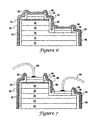
- FIG. 4illustrates a vertical topology, blue LED after coating with a passivation material
- FIG. 5illustrates the LED of FIG. 4 after patterning of the passivation material
- FIG. 6illustrates the LED of FIG. 5 after forming of a thin film
- FIG. 7illustrates the LED of FIG. 6 after patterning of the thin film and after bonding wires are connected
- FIG. 8illustrates the LED of FIG. 7 after a second coating of a passivation material
- FIG. 9illustrates an alternative embodiment LED that is in accord with the principles of the present invention.
- FIG. 10illustrates an alternative vertical LED chip configuration.
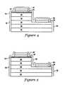
- FIGS. 2 and 3illustrate suitable blue-LED chips.
- FIG. 2illustrates a lateral topology blue-LED chip 30 that is fabricated on a sapphire substrate 32 .
- An n-GaN buffer layer 34is formed on the substrate 32 .
- a relatively thick n-GaN epitaxial layer 36is then formed on the buffer layer 34 .
- An active layer 38 having multiple quantum wells of aluminum-indium-gallium-nitride (AlInGaN) or of InGaN/GaNis then formed on the n-type GaN epitaxial layer 36 .
- a p-GaN layer 40is then formed on the active layer 38 .
- a transparent conductive layer 42is then formed on the p-GaN layer 40 .
- the transparent conductive layer 42may be made of any suitable material, such as Ru/Au, Ni/Au or indium-tin-oxide (ITO).
- a p-type electrode 44is then formed on one side of the transparent conductive layer 42 . Suitable p-type electrode materials include Ni/Au, Pd/Au, Pd/Ni and Pt.
- a p contact pad 46is then formed on the p-type electrode 44 .
- the p contact pad 46is Au.
- the transparent conductive layer 42 , the p-GaN layer 40 , the active layer 38 and part of the n-GaN layer 36are then etched to form a step. Because of the difficulty of wet etching GaN, a dry etch is beneficially usually used to form the step.
- the LED 30is then completed by forming an n-electrode pad 48 (such as Cr or Au) and an n contact pad 50 (such as Au) on the step.
- FIG. 3illustrates an alternative blue LED, specifically a vertical topology GaN-based LED 54 .
- An example of this alternative blue LED structureis disclosed in U.S. application Ser. No. 09/905,969 entitled “DIODE HAVING HIGH BRIGHTNESS AND METHOD THEREOF” filed on Jul. 17, 2001, and U.S. application Ser. No. 09/983,994 entitled “DIODE HAVING VERTICAL STRUCTURE AND METHOD OF MANUFACTURING THE SAME” filed on Oct. 26, 2001, both of which are incorporated in this application as if fully set forth herein.
- the LED 54is partially fabricated on a sapphire substrate that is subsequently removed. Removal of sapphire substrate may be done by, for example, laser lift-off.
- the LED 54includes a GaN buffer layer 55 having an n-metal contact 56 on a bottom surface and a relatively thick n-GaN layer 58 on the other.
- the n-metal contact 56is beneficially formed from a high reflective layer that is overlaid by a high conductivity metal (beneficially Au) to form an n contact pad 57 .
- An active layer 60 having a multiple quantum wellis formed on the n-type GaN layer 58 , and a p-GaN layer 62 is formed on the active layer 60 .
- a transparent conductive layer 64is then formed on the p-GaN layer 62 , and a p-type electrode 66 is formed on the transparent conductive layer 64 .
- a p contact pad 68is then formed on the p-type electrode 66 .
- the vertical GaN-based LED 54has advantages in that step etching is not required. However, to locate the n-metal contact 56 below the GaN buffer layer 55 , the sapphire substrate (not shown) that is used for initial GaN growth is removed. Sapphire substrate removal using laser lift-off is known, reference U.S. Pat. No. 6,071,795 to Cheung et al., entitled, “Separation of Thin Films From Transparent Substrates By Selective Optical Processing,” issued on Jun. 6, 2000, and Kelly et al. “Optical process for liftoff of group III-nitride films”, Physica Status Solidi (a) vol. 159, 1997, pp. R3-R4).
- the vertical GaN-based LED 54is preferred. Reasons for this include the fact that a 2′′ diameter sapphire wafer has the potential to produce about 35,000 vertical GaN-based LEDs, but only about 12,000 lateral GaN-based LEDs. Furthermore, the lateral topology is more vulnerable to static electricity, primarily because the two electrodes/pads ( 44 / 46 and 48 / 50 ) are close together. Additionally, as the lateral topology is fabricated on an insulating substrate, and as the vertical topology can be attached to a heat sink, the lateral topology has relatively poor thermal dissipation.
- a passivation layer 80is formed over the blue LED chip 30 .
- a suitable passivation layer 80may be an SiO 2 or Si x N y layer of 1000 ⁇ -thick, for example, formed on exposed surfaces of the LED chip 30 using PECVD.
- the passivation layer 80may be formed by sputtering, electron beam evaporation, or by coating with a suitable protective material, such as epoxy or flowable SiO 2 . Note that spin-coating is a particularly useful coating technique.
- PECVDis beneficial because it can form the passivation layer 80 on the sidewalls of the blue LED chip 30 .
- the passivation layer 80is then patterned to expose the p and n contact pads 46 and 50 using a suitable etchant.
- a suitable etchantFor example, BOE, HF, and/or photo-resist stripping can be used to expose the pads.
- a thin film layer 86 of, for example, a fluorescent material (such as phosphor or a tin-containing compound)is formed on the passivation layer 80 so as to cover the blue LED element.
- a fluorescent materialsuch as phosphor or a tin-containing compound
- Other suitable materialscan be used for the thin film layer 86 to convert a light of first wavelength (a first color) to a light of second wavelength (a second color).
- a blue LEDis used and coated with a phosphor thin film, for example, in accordance with the present invention, the blue light would be converted to white light by the phosphor, thus producing an “on-chip” white LED.
- Using different color LEDs and different color influencing materialswould result in different colors produced directly from the chip.
- the thin film layeris beneficially formed using metal organic chemical vapor deposition (MOCVD), atomic layer chemical vapor deposition (ALD), plasma enhanced MOCVD, plasma enhanced ALD, photo enhanced CVD, or other chemical vapor deposition methods.
- MOCVDmetal organic chemical vapor deposition
- ALDatomic layer chemical vapor deposition
- plasma enhanced MOCVDplasma enhanced ALD
- photo enhanced CVDor other chemical vapor deposition methods.
- the thin film layer 86is about 10 ⁇ m or so thick.
- the thin film layer 86is an integral element of the chip, and not part of a package.
- the film thicknessin general the thinner the better. The thickness can be reduced by growing dense thin film layers.
- the thin film layer 86is patterned to expose the p and n contact pads 46 and 50 using a suitable solvent (which will depend on the composition of the thin film layer 86 ). Bonding wires 90 and 92 are then bonded to the p and n contact pads 46 and 50 , respectively.
- an optional second passivation layer 94(which is optically transparent) is then formed over the structure of FIG. 7 .
- the first and second passivation layers 80 and 94are formed using the same process. The result is a white LED 100 .
- the white LED 100can then be encapsulated into a package, such as a lamp package or a surface mount package. However, the white LED 100 also can be used unpackaged and/or as part of another assembly.
- a reflectorbetween a contact pad and an adjacent semiconductor layer.
- a vertical LED 54as shown in FIG. 3
- a reflective layer 104between the n-metal contact 56 and the n contact pad 57 .
- the second passivation layer 94is beneficially over the p contact pad 68 .
- the second passivation layer 94is optional.
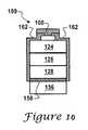
- FIG. 10illustrates a vertical LED chip configuration 199 which is an alternative to the vertical LED chip configuration 54 shown in FIGS. 3 and 9 . It should be noted that LED chip 199 of FIG. 10 is identical to the LED chip 199 of FIG. 15 in U.S. application Ser. No. 10/118,316, the entire contents of which have been incorporated by reference, as stated above.
- the LED chip 199 illustrated in FIG. 10is a vertical GaN LED chip. It comprises, among other things, a semiconductor structure that includes an n-GaN buffer layer 124 , an InGaN/GaN active layer 126 and a p-GaN contact layer 128 , where the thickness of the semiconductor structure is less than about 5 ⁇ m.
- the LED chip 199further includes a p-contact 150 and a metal support layer 156 over the p-contact 150 , where the thickness of the p-contact 150 may be less than 10 nm, and where the thickness of the metal support layer 156 is approximately 50 ⁇ m and is inherently a conductive support structure.
- a metal coatingmay be applied to the p-contact 150 .
- the p-contact 150may, for example, comprise Pt/Au, Pd/Au, Ru/Au, Ni/Au, Cr/Au or indium tin oxide (ITO)/Au, whereas the metal support layer 156 may comprise Cu, Cr, Ni, Au, Ag, Mo, Pt, Pd, W, and/or Al. Alternatively, the metal support layer 156 may comprise a metal-containing material such as titanium nitride.
- an n-type ohmic contact 160is formed on the n-GaN buffer layer 124 , where the n-type ohmic contact 160 may comprise Ti and/or Al.
- a metal pad 164comprising, for example, Cr and/or Au may be formed over the n-type ohmic contact 160 .
- FIG. 10shows a passivation layer 162 used in conjunction with the LED chip 199 .
Landscapes
- Engineering & Computer Science (AREA)
- Computer Hardware Design (AREA)
- Microelectronics & Electronic Packaging (AREA)
- Power Engineering (AREA)
- Led Devices (AREA)
- Led Device Packages (AREA)
Abstract
Description
Claims (76)
Priority Applications (1)
| Application Number | Priority Date | Filing Date | Title |
|---|---|---|---|
| US12/654,988US8288787B2 (en) | 2002-06-26 | 2010-01-12 | Thin film light emitting diode |
Applications Claiming Priority (4)
| Application Number | Priority Date | Filing Date | Title |
|---|---|---|---|
| US10/179,010US6841802B2 (en) | 2002-06-26 | 2002-06-26 | Thin film light emitting diode |
| US10/975,095US7691650B2 (en) | 2002-06-26 | 2004-10-28 | Thin film light emitting diode |
| US11/978,680US7649210B2 (en) | 2002-06-26 | 2007-10-30 | Thin film light emitting diode |
| US12/654,988US8288787B2 (en) | 2002-06-26 | 2010-01-12 | Thin film light emitting diode |
Related Parent Applications (1)
| Application Number | Title | Priority Date | Filing Date |
|---|---|---|---|
| US11/978,680ContinuationUS7649210B2 (en) | 2002-06-26 | 2007-10-30 | Thin film light emitting diode |
Publications (2)
| Publication Number | Publication Date |
|---|---|
| US20100207145A1 US20100207145A1 (en) | 2010-08-19 |
| US8288787B2true US8288787B2 (en) | 2012-10-16 |
Family
ID=32907258
Family Applications (12)
| Application Number | Title | Priority Date | Filing Date |
|---|---|---|---|
| US10/179,010Expired - LifetimeUS6841802B2 (en) | 2002-06-26 | 2002-06-26 | Thin film light emitting diode |
| US10/975,095Expired - LifetimeUS7691650B2 (en) | 2002-06-26 | 2004-10-28 | Thin film light emitting diode |
| US11/978,680Expired - LifetimeUS7649210B2 (en) | 2002-06-26 | 2007-10-30 | Thin film light emitting diode |
| US12/591,165Expired - Fee RelatedUS8445921B2 (en) | 2002-06-26 | 2009-11-10 | Thin film light emitting diode |
| US12/591,164Expired - Fee RelatedUS8384091B2 (en) | 2002-06-26 | 2009-11-10 | Thin film light emitting diode |
| US12/654,988Expired - Fee RelatedUS8288787B2 (en) | 2002-06-26 | 2010-01-12 | Thin film light emitting diode |
| US12/654,992Expired - Fee RelatedUS7956364B2 (en) | 2002-06-26 | 2010-01-12 | Thin film light emitting diode |
| US13/110,545Expired - Fee RelatedUS8207552B2 (en) | 2002-06-26 | 2011-05-18 | Thin film light emitting diode |
| US13/855,637Expired - Fee RelatedUS9281454B2 (en) | 2002-06-26 | 2013-04-02 | Thin film light emitting diode |
| US15/008,091Expired - Fee RelatedUS9716213B2 (en) | 2002-06-26 | 2016-01-27 | Thin film light emitting diode |
| US15/633,440Expired - Fee RelatedUS10326059B2 (en) | 2002-06-26 | 2017-06-26 | Thin film light emitting diode |
| US16/405,758Expired - Fee RelatedUS10825962B2 (en) | 2002-06-26 | 2019-05-07 | Thin film light emitting diode |
Family Applications Before (5)
| Application Number | Title | Priority Date | Filing Date |
|---|---|---|---|
| US10/179,010Expired - LifetimeUS6841802B2 (en) | 2002-06-26 | 2002-06-26 | Thin film light emitting diode |
| US10/975,095Expired - LifetimeUS7691650B2 (en) | 2002-06-26 | 2004-10-28 | Thin film light emitting diode |
| US11/978,680Expired - LifetimeUS7649210B2 (en) | 2002-06-26 | 2007-10-30 | Thin film light emitting diode |
| US12/591,165Expired - Fee RelatedUS8445921B2 (en) | 2002-06-26 | 2009-11-10 | Thin film light emitting diode |
| US12/591,164Expired - Fee RelatedUS8384091B2 (en) | 2002-06-26 | 2009-11-10 | Thin film light emitting diode |
Family Applications After (6)
| Application Number | Title | Priority Date | Filing Date |
|---|---|---|---|
| US12/654,992Expired - Fee RelatedUS7956364B2 (en) | 2002-06-26 | 2010-01-12 | Thin film light emitting diode |
| US13/110,545Expired - Fee RelatedUS8207552B2 (en) | 2002-06-26 | 2011-05-18 | Thin film light emitting diode |
| US13/855,637Expired - Fee RelatedUS9281454B2 (en) | 2002-06-26 | 2013-04-02 | Thin film light emitting diode |
| US15/008,091Expired - Fee RelatedUS9716213B2 (en) | 2002-06-26 | 2016-01-27 | Thin film light emitting diode |
| US15/633,440Expired - Fee RelatedUS10326059B2 (en) | 2002-06-26 | 2017-06-26 | Thin film light emitting diode |
| US16/405,758Expired - Fee RelatedUS10825962B2 (en) | 2002-06-26 | 2019-05-07 | Thin film light emitting diode |
Country Status (1)
| Country | Link |
|---|---|
| US (12) | US6841802B2 (en) |
Cited By (7)
| Publication number | Priority date | Publication date | Assignee | Title |
|---|---|---|---|---|
| US20110220948A1 (en)* | 2001-07-17 | 2011-09-15 | Yoo Myung Cheol | Diode having high brightness and method thereof |
| US20130049063A1 (en)* | 2010-04-28 | 2013-02-28 | Mitsubishi Heavy Industries, Ltd. | Semiconductor light-emitting element, protective film for semiconductor light-emitting element, and process for production of the protective film |
| US8759129B2 (en) | 2001-10-22 | 2014-06-24 | Lg Innotek Co., Ltd | Method of making diode having reflective layer |
| US9000468B2 (en) | 2001-10-26 | 2015-04-07 | Lg Innotek Co., Ltd. | Diode having vertical structure |
| US20150311400A1 (en)* | 2012-02-13 | 2015-10-29 | Epistar Corporation | Light-emitting device |
| KR20160045085A (en)* | 2013-08-21 | 2016-04-26 | 오스람 옵토 세미컨덕터스 게엠베하 | Method for producing an optoelectronic semiconductor chip |
| US9666761B2 (en)* | 2015-09-10 | 2017-05-30 | Kabushiki Kaisha Toshiba | Light-emitting device |
Families Citing this family (102)
| Publication number | Priority date | Publication date | Assignee | Title |
|---|---|---|---|---|
| US6841802B2 (en) | 2002-06-26 | 2005-01-11 | Oriol, Inc. | Thin film light emitting diode |
| US6744196B1 (en)* | 2002-12-11 | 2004-06-01 | Oriol, Inc. | Thin film LED |
| DE10259946A1 (en)* | 2002-12-20 | 2004-07-15 | Tews, Walter, Dipl.-Chem. Dr.rer.nat.habil. | Phosphors for converting the ultraviolet or blue emission of a light-emitting element into visible white radiation with very high color rendering |
| US7423296B2 (en)* | 2003-02-26 | 2008-09-09 | Avago Technologies Ecbu Ip Pte Ltd | Apparatus for producing a spectrally-shifted light output from a light emitting device utilizing thin-film luminescent layers |
| JP2005026688A (en)* | 2003-06-30 | 2005-01-27 | Osram Opto Semiconductors Gmbh | Radiation emitting semiconductor chip, method for manufacturing the semiconductor chip, and method for adjusting and setting the brightness of the semiconductor chip |
| US7915085B2 (en) | 2003-09-18 | 2011-03-29 | Cree, Inc. | Molded chip fabrication method |
| TWI229463B (en)* | 2004-02-02 | 2005-03-11 | South Epitaxy Corp | Light-emitting diode structure with electro-static discharge protection |
| DE102004029412A1 (en)* | 2004-02-27 | 2005-10-13 | Osram Opto Semiconductors Gmbh | Radiation-emitting semiconductor chip and method for producing such a semiconductor chip |
| KR100611055B1 (en)* | 2004-03-25 | 2006-08-10 | 학교법인 포항공과대학교 | Display device by using photonic quantum ring laser |
| US20050224812A1 (en)* | 2004-03-31 | 2005-10-13 | Yu-Chuan Liu | Light-emitting device and manufacturing process of the light-emitting device |
| US20050236630A1 (en)* | 2004-04-23 | 2005-10-27 | Wang-Nang Wang | Transparent contact for light emitting diode |
| US7323721B2 (en)* | 2004-09-09 | 2008-01-29 | Blue Photonics Inc. | Monolithic multi-color, multi-quantum well semiconductor LED |
| TWI352437B (en) | 2007-08-27 | 2011-11-11 | Epistar Corp | Optoelectronic semiconductor device |
| DE102005019376A1 (en)* | 2005-04-26 | 2006-11-02 | Patent-Treuhand-Gesellschaft für elektrische Glühlampen mbH | Luminescence conversion light emitting diode has conversion unit formed by luminescent substances in which one substance emits red and another substance emits yellow to green, where former substance is alone directly applied on chip |
| DE102005038698A1 (en)* | 2005-07-08 | 2007-01-18 | Tridonic Optoelectronics Gmbh | Optoelectronic components with adhesion promoter |
| KR100658970B1 (en)* | 2006-01-09 | 2006-12-19 | 주식회사 메디아나전자 | Light Emitting Diodes Generate Complex Light |
| US8044412B2 (en) | 2006-01-20 | 2011-10-25 | Taiwan Semiconductor Manufacturing Company, Ltd | Package for a light emitting element |
| JP5162909B2 (en)* | 2006-04-03 | 2013-03-13 | 豊田合成株式会社 | Semiconductor light emitting device |
| US8969908B2 (en) | 2006-04-04 | 2015-03-03 | Cree, Inc. | Uniform emission LED package |
| US20080048178A1 (en) | 2006-08-24 | 2008-02-28 | Bruce Gardiner Aitken | Tin phosphate barrier film, method, and apparatus |
| WO2008045423A1 (en)* | 2006-10-10 | 2008-04-17 | Structured Materials Inc. | Self assembled controlled luminescent transparent conductive photonic crystals for light emitting devices |
| US10295147B2 (en) | 2006-11-09 | 2019-05-21 | Cree, Inc. | LED array and method for fabricating same |
| US9024349B2 (en) | 2007-01-22 | 2015-05-05 | Cree, Inc. | Wafer level phosphor coating method and devices fabricated utilizing method |
| US8546818B2 (en) | 2007-06-12 | 2013-10-01 | SemiLEDs Optoelectronics Co., Ltd. | Vertical LED with current-guiding structure |
| US8148733B2 (en) | 2007-06-12 | 2012-04-03 | SemiLEDs Optoelectronics Co., Ltd. | Vertical LED with current guiding structure |
| US7759670B2 (en)* | 2007-06-12 | 2010-07-20 | SemiLEDs Optoelectronics Co., Ltd. | Vertical LED with current guiding structure |
| TWI411124B (en)* | 2007-07-10 | 2013-10-01 | Delta Electronics Inc | Light-emitting diode device and method of manufacturing same |
| US7863635B2 (en)* | 2007-08-07 | 2011-01-04 | Cree, Inc. | Semiconductor light emitting devices with applied wavelength conversion materials |
| EP2206164A2 (en)* | 2007-10-08 | 2010-07-14 | 3M Innovative Properties Company | Light emitting diode with bonded semiconductor wavelength converter |
| JP2011501466A (en)* | 2007-10-26 | 2011-01-06 | クリー エル イー ディー ライティング ソリューションズ インコーポレイテッド | Lighting device having one or more light emitters and method of making the same |
| US8878219B2 (en)* | 2008-01-11 | 2014-11-04 | Cree, Inc. | Flip-chip phosphor coating method and devices fabricated utilizing method |
| JP5221166B2 (en)* | 2008-02-20 | 2013-06-26 | スタンレー電気株式会社 | ZnO-based semiconductor element, manufacturing method thereof, and optical semiconductor element |
| US8637883B2 (en) | 2008-03-19 | 2014-01-28 | Cree, Inc. | Low index spacer layer in LED devices |
| US8829554B2 (en)* | 2008-04-02 | 2014-09-09 | Lg Innotek Co., Ltd. | Light emitting element and a production method therefor |
| KR20090106299A (en)* | 2008-04-05 | 2009-10-08 | 송준오 | Group III-nitride semiconductor light emitting diode device having an ohmic contact light extracting structure layer and a method of manufacturing the same |
| WO2009125953A2 (en)* | 2008-04-06 | 2009-10-15 | Song June O | Luminous element |
| CN102067337A (en)* | 2008-08-19 | 2011-05-18 | 晶能光电(江西)有限公司 | Semiconductor light-emitting device with silicone protective layer |
| JP5305790B2 (en)* | 2008-08-28 | 2013-10-02 | 株式会社東芝 | Semiconductor light emitting device |
| TW201015743A (en)* | 2008-10-01 | 2010-04-16 | Formosa Epitaxy Inc | LED and manufacturing method thereof |
| US20100119839A1 (en) | 2008-11-13 | 2010-05-13 | Maven Optronics Corp. | System and Method for Forming a Thin-Film Phosphor Layer for Phosphor-Converted Light Emitting Devices |
| KR20110105842A (en)* | 2008-12-24 | 2011-09-27 | 쓰리엠 이노베이티브 프로퍼티즈 컴파니 | Light-generating element with double sided wavelength converter |
| KR20110099761A (en) | 2008-12-24 | 2011-09-08 | 쓰리엠 이노베이티브 프로퍼티즈 컴파니 | Double-sided wavelength converter and method of manufacturing light generating device using same |
| DE102009001028B4 (en)* | 2009-02-20 | 2011-02-17 | Infineon Technologies Ag | Method for producing a bond connection |
| US8138509B2 (en)* | 2009-02-27 | 2012-03-20 | Visera Technologies Company, Limited | Light emitting device having luminescent layer with opening to exposed bond pad on light emitting die for wire bonding pad to substrate |
| TWI407596B (en)* | 2009-03-06 | 2013-09-01 | Advanced Optoelectronic Tech | Side heat-dissipating light-emitting diode and its manufacturing process |
| US20100264435A1 (en)* | 2009-04-21 | 2010-10-21 | Bily Wang | White light-emitting diode package structure for simplifying package process and method for making the same |
| US9647239B2 (en)* | 2009-05-08 | 2017-05-09 | Koninklijke Philips N.V. | Electroluminescent device |
| US8921876B2 (en) | 2009-06-02 | 2014-12-30 | Cree, Inc. | Lighting devices with discrete lumiphor-bearing regions within or on a surface of remote elements |
| DE102009033686A1 (en)* | 2009-07-17 | 2011-01-20 | Osram Opto Semiconductors Gmbh | Optoelectronic semiconductor component and method for producing an inorganic optoelectronic semiconductor component |
| US9502612B2 (en) | 2009-09-20 | 2016-11-22 | Viagan Ltd. | Light emitting diode package with enhanced heat conduction |
| DE102009058796A1 (en)* | 2009-12-18 | 2011-06-22 | OSRAM Opto Semiconductors GmbH, 93055 | Optoelectronic component and method for producing an optoelectronic component |
| CN102263184A (en)* | 2009-12-30 | 2011-11-30 | 宝霖科技股份有限公司 | Method and structure for manufacturing a light-emitting diode |
| KR100999779B1 (en)* | 2010-02-01 | 2010-12-08 | 엘지이노텍 주식회사 | Light emitting device, manufacturing method and light emitting device package |
| US8981397B2 (en)* | 2010-02-12 | 2015-03-17 | Tsmc Solid State Lighting Ltd. | Light-emitting devices on textured substrates |
| US9275979B2 (en) | 2010-03-03 | 2016-03-01 | Cree, Inc. | Enhanced color rendering index emitter through phosphor separation |
| US8450770B2 (en)* | 2010-05-11 | 2013-05-28 | Advanced Semiconductor Engineering, Inc. | Light emitting package structure |
| WO2011145794A1 (en)* | 2010-05-18 | 2011-11-24 | 서울반도체 주식회사 | Light emitting diode chip having wavelength conversion layer and manufacturing method thereof, and package including same and manufacturing method thereof |
| KR101662010B1 (en)* | 2010-05-20 | 2016-10-05 | 엘지이노텍 주식회사 | Light Emitting Device |
| US8471282B2 (en) | 2010-06-07 | 2013-06-25 | Koninklijke Philips Electronics N.V. | Passivation for a semiconductor light emitting device |
| KR100988194B1 (en) | 2010-07-26 | 2010-10-18 | (주)더리즈 | Semiconductor light emitting device and method of fabricating the same |
| DE102010044560A1 (en) | 2010-09-07 | 2012-03-08 | Osram Opto Semiconductors Gmbh | Method for producing an optoelectronic semiconductor component |
| US8563334B2 (en)* | 2010-09-14 | 2013-10-22 | Tsmc Solid State Lighting Ltd. | Method to remove sapphire substrate |
| JP5921550B2 (en) | 2010-09-22 | 2016-05-24 | コーニンクレッカ フィリップス エヌ ヴェKoninklijke Philips N.V. | Multi-view display device |
| JP5545866B2 (en)* | 2010-11-01 | 2014-07-09 | シチズン電子株式会社 | Semiconductor light emitting device |
| US9166126B2 (en) | 2011-01-31 | 2015-10-20 | Cree, Inc. | Conformally coated light emitting devices and methods for providing the same |
| US11251164B2 (en) | 2011-02-16 | 2022-02-15 | Creeled, Inc. | Multi-layer conversion material for down conversion in solid state lighting |
| JP5754173B2 (en)* | 2011-03-01 | 2015-07-29 | ソニー株式会社 | Light emitting unit and display device |
| CN102683514B (en) | 2011-03-06 | 2017-07-14 | 维亚甘有限公司 | LED package and manufacture method |
| DE102011016935A1 (en)* | 2011-04-13 | 2012-10-18 | Osram Opto Semiconductors Gmbh | A method of manufacturing a semiconductor light emitting device and light emitting semiconductor device |
| KR101791175B1 (en)* | 2011-06-30 | 2017-10-27 | 엘지이노텍 주식회사 | Light emitting device and light emitting device package including the same |
| TWI484672B (en)* | 2011-08-29 | 2015-05-11 | Genesis Photonics Inc | Light emitting diode structure and fabricating method thereof |
| US8349116B1 (en) | 2011-11-18 | 2013-01-08 | LuxVue Technology Corporation | Micro device transfer head heater assembly and method of transferring a micro device |
| US8573469B2 (en) | 2011-11-18 | 2013-11-05 | LuxVue Technology Corporation | Method of forming a micro LED structure and array of micro LED structures with an electrically insulating layer |
| US8794501B2 (en)* | 2011-11-18 | 2014-08-05 | LuxVue Technology Corporation | Method of transferring a light emitting diode |
| US8333860B1 (en) | 2011-11-18 | 2012-12-18 | LuxVue Technology Corporation | Method of transferring a micro device |
| TWI447975B (en)* | 2012-01-05 | 2014-08-01 | 矽品精密工業股份有限公司 | Structure of light-emitting diode chip, structure of light-emitting diode package substrate, light-emitting diode package structure and preparation method thereof |
| TWI479694B (en) | 2012-01-11 | 2015-04-01 | Formosa Epitaxy Inc | Light emitting diode wafers |
| WO2013118072A2 (en) | 2012-02-10 | 2013-08-15 | Koninklijke Philips N.V. | Wavelength converted light emitting device |
| US20140151630A1 (en)* | 2012-12-04 | 2014-06-05 | Feng-Hsu Fan | Protection for the epitaxial structure of metal devices |
| US9548424B2 (en) | 2013-02-04 | 2017-01-17 | Industrial Technology Research Institute | Light emitting diode |
| TWI557942B (en) | 2013-02-04 | 2016-11-11 | 財團法人工業技術研究院 | Light-emitting diode |
| US9425359B2 (en) | 2013-02-04 | 2016-08-23 | Industrial Technology Research Institute | Light emitting diode |
| KR101967837B1 (en)* | 2013-03-11 | 2019-04-10 | 삼성전자주식회사 | Semiconductor light-emitting device |
| DE102013103079A1 (en)* | 2013-03-26 | 2014-10-02 | Osram Opto Semiconductors Gmbh | Optoelectronic semiconductor chip and method for producing an optoelectronic semiconductor chip |
| CN104183681A (en)* | 2013-05-22 | 2014-12-03 | 展晶科技(深圳)有限公司 | Light-emitting-diode chip |
| DE102013107531A1 (en)* | 2013-07-16 | 2015-01-22 | Osram Opto Semiconductors Gmbh | Optoelectronic semiconductor chip |
| JP6301097B2 (en)* | 2013-10-01 | 2018-03-28 | シチズン電子株式会社 | Semiconductor light emitting device |
| JP2015082612A (en)* | 2013-10-23 | 2015-04-27 | 旭化成株式会社 | Nitride light-emitting element and method of manufacturing the same |
| KR20150122360A (en)* | 2014-04-23 | 2015-11-02 | (주)라이타이저코리아 | Package for Light Emitting Device and Method for Manufacturing thereof |
| JP6507007B2 (en)* | 2015-03-27 | 2019-04-24 | 東レエンジニアリング株式会社 | LED module and method of manufacturing LED module |
| CN104952995B (en)* | 2015-05-05 | 2017-08-25 | 湘能华磊光电股份有限公司 | A kind of inverted structure of III light emitting semiconductor device |
| KR102316325B1 (en)* | 2015-07-06 | 2021-10-22 | 엘지전자 주식회사 | Display device using semiconductor light emitting device and method for manufacturing |
| CN105609603A (en)* | 2016-03-02 | 2016-05-25 | 厦门乾照光电股份有限公司 | Nitride buffer layer with composite structure |
| RU2657497C1 (en)* | 2017-05-12 | 2018-06-14 | Сиа Эволед | Method for producing emission layer based on compounds of rare-earth elements and organic light-emitting diodes |
| US11469138B2 (en)* | 2018-05-04 | 2022-10-11 | Taiwan Semiconductor Manufacturing Company, Ltd. | Via for coupling attached component upper electrode to substrate |
| DE102018118962A1 (en)* | 2018-08-03 | 2020-02-06 | Osram Opto Semiconductors Gmbh | ELECTROMAGNETIC RADIATION EMITTING COMPONENT AND METHOD FOR APPLYING A CONVERTER LAYER TO AN ELECTROMAGNETIC RADIATION EMITTING COMPONENT |
| CN109119436B (en)* | 2018-09-29 | 2024-04-09 | 华南理工大学 | Surface roughened nano-pore LED array chip and preparation method thereof |
| CN111048496B (en)* | 2018-10-12 | 2021-08-31 | 中国科学院半导体研究所 | Flip-chip LED red light device structure and preparation method thereof |
| KR20200088948A (en)* | 2019-01-15 | 2020-07-24 | 삼성디스플레이 주식회사 | A light emitting diode and display device comprising the same |
| CN110828629B (en)* | 2019-10-22 | 2024-02-20 | 佛山市国星半导体技术有限公司 | A flip-chip LED chip and its manufacturing method |
| KR102858002B1 (en)* | 2020-08-10 | 2025-09-12 | 삼성디스플레이 주식회사 | Light emitting element, display device using the light emitting element, and method of fabricating the display device |
| JP7472354B1 (en) | 2023-04-04 | 2024-04-22 | 日機装株式会社 | Semiconductor light emitting device and method for manufacturing the same |
Citations (261)
| Publication number | Priority date | Publication date | Assignee | Title |
|---|---|---|---|---|
| US2913358A (en) | 1958-07-21 | 1959-11-17 | Pacific Semiconductors Inc | Method for forming passivation films on semiconductor bodies and articles resulting therefrom |
| US2981877A (en) | 1959-07-30 | 1961-04-25 | Fairchild Semiconductor | Semiconductor device-and-lead structure |
| US3602982A (en) | 1967-05-13 | 1971-09-07 | Philips Corp | Method of manufacturing a semiconductor device and device manufactured by said method |
| US3774086A (en) | 1972-09-25 | 1973-11-20 | Gen Electric | Solid state lamp having visible-emitting phosphor at edge of infrated-emitting element |
| US3875456A (en) | 1972-04-04 | 1975-04-01 | Hitachi Ltd | Multi-color semiconductor lamp |
| US3907620A (en) | 1973-06-27 | 1975-09-23 | Hewlett Packard Co | A process of forming metallization structures on semiconductor devices |
| US4141135A (en) | 1975-10-14 | 1979-02-27 | Thomson-Csf | Semiconductor process using lapped substrate and lapped low resistivity semiconductor carrier |
| US4406052A (en) | 1981-11-12 | 1983-09-27 | Gte Laboratories Incorporated | Non-epitaxial static induction transistor processing |
| US4634926A (en) | 1984-07-20 | 1987-01-06 | U.S. Philips Corporation | Display tube provided with an interference filter |
| US4882617A (en) | 1986-12-24 | 1989-11-21 | U.S. Philips Corporation | Projection device and associated electro-optic monochrome display device with phosphor layer and interference filters |
| US4918497A (en) | 1988-12-14 | 1990-04-17 | Cree Research, Inc. | Blue light emitting diode formed in silicon carbide |
| US4966862A (en) | 1989-08-28 | 1990-10-30 | Cree Research, Inc. | Method of production of light emitting diodes |
| US5027168A (en) | 1988-12-14 | 1991-06-25 | Cree Research, Inc. | Blue light emitting diode formed in silicon carbide |
| US5034068A (en) | 1990-02-23 | 1991-07-23 | Spectrolab, Inc. | Photovoltaic cell having structurally supporting open conductive back electrode structure, and method of fabricating the cell |
| US5040044A (en) | 1989-06-21 | 1991-08-13 | Mitsubishi Monsanto Chemical Company | Compound semiconductor device and method for surface treatment |
| US5162876A (en) | 1990-09-28 | 1992-11-10 | Kabushiki Kaisha Toshiba | Semiconductor device having high breakdown voltage |
| US5198795A (en) | 1990-04-04 | 1993-03-30 | Asahi Kasei Kogyo Kabushiki Kaisha | Magnetoelectric transducer and process for producing the same |
| US5210051A (en) | 1990-03-27 | 1993-05-11 | Cree Research, Inc. | High efficiency light emitting diodes from bipolar gallium nitride |
| US5382452A (en) | 1992-12-18 | 1995-01-17 | E. I. Du Pont De Nemours And Company | Luminescent materials prepared by coating luminescent compositions onto substrate particles |
| US5429954A (en) | 1993-02-20 | 1995-07-04 | Temic Telefunken Microelectronic Gmbh | Radiation-emitting diode with improved radiation output |
| US5454915A (en) | 1992-10-06 | 1995-10-03 | Kulite Semiconductor Products, Inc. | Method of fabricating porous silicon carbide (SiC) |
| US5504036A (en) | 1994-05-24 | 1996-04-02 | U.S. Philips Corporation | Method of manufacturing semiconductor devices with semiconductor elements formed in a layer of semiconductor material provided on a support slice |
| US5523589A (en) | 1994-09-20 | 1996-06-04 | Cree Research, Inc. | Vertical geometry light emitting diode with group III nitride active layer and extended lifetime |
| US5554418A (en) | 1993-12-28 | 1996-09-10 | Nihon Shinku Gijutsu Kabushiki Kaisha | Method of forming passivation film |
| US5585648A (en) | 1995-02-03 | 1996-12-17 | Tischler; Michael A. | High brightness electroluminescent device, emitting in the green to ultraviolet spectrum, and method of making the same |
| US5592501A (en) | 1994-09-20 | 1997-01-07 | Cree Research, Inc. | Low-strain laser structures with group III nitride active layers |
| US5620557A (en) | 1993-12-27 | 1997-04-15 | Toyoda Gosei Co., Ltd. | Sapphireless group III nitride semiconductor and method for making same |
| US5631664A (en) | 1992-09-18 | 1997-05-20 | Olympus Optical Co., Ltd. | Display system utilizing electron emission by polarization reversal of ferroelectric material |
| US5644190A (en) | 1995-07-05 | 1997-07-01 | Advanced Vision Technologies, Inc. | Direct electron injection field-emission display device |
| US5661074A (en) | 1995-02-03 | 1997-08-26 | Advanced Technology Materials, Inc. | High brightness electroluminescent device emitting in the green to ultraviolet spectrum and method of making the same |
| US5684309A (en) | 1996-07-11 | 1997-11-04 | North Carolina State University | Stacked quantum well aluminum indium gallium nitride light emitting diodes |
| US5693963A (en) | 1994-09-19 | 1997-12-02 | Kabushiki Kaisha Toshiba | Compound semiconductor device with nitride |
| WO1997050132A1 (en) | 1996-06-26 | 1997-12-31 | Siemens Aktiengesellschaft | Light-emitting semiconductor component with luminescence conversion element |
| DE19625622A1 (en) | 1996-06-26 | 1998-01-02 | Siemens Ag | Light radiating semiconductor constructional element |
| US5707745A (en) | 1994-12-13 | 1998-01-13 | The Trustees Of Princeton University | Multicolor organic light emitting devices |
| US5712504A (en) | 1995-02-02 | 1998-01-27 | Sumitomo Electric Industries, Ltd. | Pin type light-receiving device, opto electronic conversion circuit, and opto-electronic conversion module |
| US5729029A (en) | 1996-09-06 | 1998-03-17 | Hewlett-Packard Company | Maximizing electrical doping while reducing material cracking in III-V nitride semiconductor devices |
| DE19638667A1 (en) | 1996-09-20 | 1998-04-02 | Siemens Ag | Mixed-color light-emitting semiconductor component with luminescence conversion element |
| US5739554A (en) | 1995-05-08 | 1998-04-14 | Cree Research, Inc. | Double heterojunction light emitting diode with gallium nitride active layer |
| US5744233A (en) | 1994-09-09 | 1998-04-28 | U.S. Philips Corporation | Method of coating luminescent powders, luminescent powders and coated object |
| JPH10150220A (en) | 1996-11-15 | 1998-06-02 | Toyoda Gosei Co Ltd | Semiconductor light emitting device |
| US5786606A (en) | 1995-12-15 | 1998-07-28 | Kabushiki Kaisha Toshiba | Semiconductor light-emitting device |
| US5798537A (en) | 1995-08-31 | 1998-08-25 | Kabushiki Kaisha Toshiba | Blue light-emitting device |
| US5804834A (en) | 1994-10-28 | 1998-09-08 | Mitsubishi Chemical Corporation | Semiconductor device having contact resistance reducing layer |
| US5813752A (en) | 1997-05-27 | 1998-09-29 | Philips Electronics North America Corporation | UV/blue LED-phosphor device with short wave pass, long wave pass band pass and peroit filters |
| US5813753A (en) | 1997-05-27 | 1998-09-29 | Philips Electronics North America Corporation | UV/blue led-phosphor device with efficient conversion of UV/blues light to visible light |
| US5847507A (en) | 1997-07-14 | 1998-12-08 | Hewlett-Packard Company | Fluorescent dye added to epoxy of light emitting diode lens |
| US5862167A (en) | 1994-07-19 | 1999-01-19 | Toyoda Gosei Co., Ltd. | Light-emitting semiconductor device using gallium nitride compound |
| US5874747A (en) | 1996-02-05 | 1999-02-23 | Advanced Technology Materials, Inc. | High brightness electroluminescent device emitting in the green to ultraviolet spectrum and method of making the same |
| US5925896A (en) | 1996-03-08 | 1999-07-20 | Nec Corporation | Surface-emitting semiconductor optical device |
| US5929466A (en) | 1994-03-09 | 1999-07-27 | Kabushiki Kaisha Toshiba | Semiconductor device and method of fabricating the same |
| US5930653A (en) | 1995-12-14 | 1999-07-27 | U.S. Philips Corporation | Method of manufacturing a semiconductor device for surface mounting suitable for comparatively high voltages, and such a semiconductor device |
| US5959316A (en) | 1998-09-01 | 1999-09-28 | Hewlett-Packard Company | Multiple encapsulation of phosphor-LED devices |
| US5959307A (en) | 1995-11-06 | 1999-09-28 | Nichia Chemical Industries Ltd. | Nitride semiconductor device |
| US5972781A (en) | 1997-09-30 | 1999-10-26 | Siemens Aktiengesellschaft | Method for producing semiconductor chips |
| US5990500A (en) | 1998-03-25 | 1999-11-23 | Kabushiki Kaisha Toshiba | Nitride compound semiconductor light emitting element and its manufacturing method |
| US5998925A (en) | 1996-07-29 | 1999-12-07 | Nichia Kagaku Kogyo Kabushiki Kaisha | Light emitting device having a nitride compound semiconductor and a phosphor containing a garnet fluorescent material |
| JP2000036626A (en) | 1999-07-26 | 2000-02-02 | Sanken Electric Co Ltd | Manufacture of light-emitting diode device |
| US6025251A (en) | 1995-09-29 | 2000-02-15 | Siemens Aktiengesellschaft | Method for producing a plurality of semiconductor components |
| US6036823A (en) | 1995-08-11 | 2000-03-14 | Denso Corporation | Dielectric thin film and thin-film EL device using same |
| JP2000077713A (en) | 1998-08-27 | 2000-03-14 | Sanyo Electric Co Ltd | Semiconductor light-emitting element |
| US6041515A (en)* | 1998-01-12 | 2000-03-28 | Life Technologies, Inc. | Apparatus for drying solutions containing macromolecules |
| US6043515A (en) | 1996-09-17 | 2000-03-28 | Kabushiki Kaisha Toshiba | Optical semiconductor device |
| JP2000101139A (en) | 1998-09-25 | 2000-04-07 | Toshiba Corp | Semiconductor light emitting element, method of manufacturing the same, and semiconductor light emitting device |
| JP2000106473A (en) | 1998-07-29 | 2000-04-11 | Sanyo Electric Co Ltd | Semiconductor device, semiconductor light emitting device and manufacture thereof, and forming method of nitride semiconductor layer |
| US6063643A (en) | 1995-09-04 | 2000-05-16 | Nec Corporation | Surface-emission type light-emitting diode and fabrication process thereof |
| US6067309A (en) | 1996-09-06 | 2000-05-23 | Kabushiki Kaisha Toshiba | Compound semiconductor light-emitting device of gallium nitride series |
| US6071795A (en) | 1998-01-23 | 2000-06-06 | The Regents Of The University Of California | Separation of thin films from transparent substrates by selective optical processing |
| US6078064A (en) | 1998-05-04 | 2000-06-20 | Epistar Co. | Indium gallium nitride light emitting diode |
| JP2000196197A (en) | 1998-12-30 | 2000-07-14 | Xerox Corp | Structure of nitride laser diode where growth substrate is eliminated and method for manufacturing nitride diode array structure |
| JP3065263B2 (en) | 1996-12-27 | 2000-07-17 | 日亜化学工業株式会社 | Light emitting device and LED display using the same |
| US6093965A (en) | 1993-04-28 | 2000-07-25 | Nichia Chemical Industries Ltd. | Gallium nitride-based III-V group compound semiconductor |
| US6096570A (en) | 1998-06-22 | 2000-08-01 | Yamaha Corporation | Field emitter having sharp tip |
| JP2000216434A (en) | 1996-12-27 | 2000-08-04 | Nichia Chem Ind Ltd | Light emitting diode and method of forming the same |
| US6100545A (en) | 1997-10-10 | 2000-08-08 | Toyoda Gosei Co., Ltd. | GaN type semiconductor device |
| US6100104A (en) | 1997-09-19 | 2000-08-08 | Siemens Aktiengesellschaft | Method for fabricating a plurality of semiconductor bodies |
| US6133589A (en) | 1999-06-08 | 2000-10-17 | Lumileds Lighting, U.S., Llc | AlGaInN-based LED having thick epitaxial layer for improved light extraction |
| US6146916A (en) | 1997-12-02 | 2000-11-14 | Murata Manufacturing Co., Ltd. | Method for forming a GaN-based semiconductor light emitting device |
| JP2000315819A (en) | 1999-04-30 | 2000-11-14 | Rohm Co Ltd | Manufacture of semiconductor light emitting element |
| JP2000323797A (en) | 1999-05-10 | 2000-11-24 | Pioneer Electronic Corp | Nitride semiconductor laser and its manufacture |
| US6155699A (en) | 1999-03-15 | 2000-12-05 | Agilent Technologies, Inc. | Efficient phosphor-conversion led structure |
| DE20009283U1 (en) | 2000-04-26 | 2000-12-28 | OSRAM Opto Semiconductors GmbH & Co. oHG, 93049 Regensburg | Radiation-emitting semiconductor component based on GaN |
| US6172382B1 (en) | 1997-01-09 | 2001-01-09 | Nichia Chemical Industries, Ltd. | Nitride semiconductor light-emitting and light-receiving devices |
| US6177684B1 (en) | 1998-03-17 | 2001-01-23 | Fujitsu Limited | Quantum semiconductor device having a quantum dot structure |
| JP2001053336A (en) | 1999-08-05 | 2001-02-23 | Toyoda Gosei Co Ltd | Group III nitride compound semiconductor light emitting device |
| DE19945007A1 (en) | 1999-09-20 | 2001-03-22 | Opto Tech Corp | Light emitting diode used in computer peripherals and instrument displays comprises an epitaxial layer, a composite layer, a conducting substrate, a counter electrode and a front electrode |
| JP2001111109A (en) | 1999-10-07 | 2001-04-20 | Sharp Corp | Gallium nitride based compound semiconductor light emitting device |
| US6229160B1 (en) | 1997-06-03 | 2001-05-08 | Lumileds Lighting, U.S., Llc | Light extraction from a semiconductor light-emitting device via chip shaping |
| US20010004112A1 (en) | 1999-12-21 | 2001-06-21 | Kabushiki Kaisha Toshiba | Semiconductor light emitting element and manufacturing method thereof |
| US6252254B1 (en) | 1998-02-06 | 2001-06-26 | General Electric Company | Light emitting device with phosphor composition |
| US6255670B1 (en) | 1998-02-06 | 2001-07-03 | General Electric Company | Phosphors for light generation from light emitting semiconductors |
| US6278136B1 (en) | 1997-04-22 | 2001-08-21 | Kabushiki Kaisha Toshiba | Semiconductor light emitting element, its manufacturing method and light emitting device |
| US6281526B1 (en) | 1997-03-05 | 2001-08-28 | Kabushiki Kaisha Toshiba | Nitride compound light emitting device and method for fabricating same |
| US20010019134A1 (en) | 1999-05-10 | 2001-09-06 | Kuo-Hsiung Chang | Light emitting diode with a permanent substrate of transparent glass or quartz and the method for manufacturing the same |
| JP2001244503A (en) | 1999-12-21 | 2001-09-07 | Nichia Chem Ind Ltd | Nitride semiconductor light emitting device |
| DE10010638A1 (en) | 2000-03-03 | 2001-09-13 | Osram Opto Semiconductors Gmbh | Making light emitting semiconducting body with luminescence conversion element involves applying suspension with solvent, adhesive, luminescent material |
| US20010022390A1 (en) | 1998-06-30 | 2001-09-20 | Gunther Waitl | Diode housing |
| US6294800B1 (en) | 1998-02-06 | 2001-09-25 | General Electric Company | Phosphors for white light generation from UV emitting diodes |
| CA2340968A1 (en) | 2000-03-27 | 2001-09-27 | General Electric Company | White light illumination system with improved color output |
| JP2001274507A (en) | 2000-03-28 | 2001-10-05 | Pioneer Electronic Corp | Nitride semiconductor laser and its manufacturing method |
| US20010028062A1 (en) | 2000-03-31 | 2001-10-11 | Toshiya Uemura | Light-emitting device using a group III nitride compound semiconductor and a method of manufacture |
| US6303404B1 (en) | 1999-05-28 | 2001-10-16 | Yong Tae Moon | Method for fabricating white light emitting diode using InGaN phase separation |
| US6310351B1 (en) | 1998-09-01 | 2001-10-30 | Edge Medical Devices, Inc. | X-ray imaging system |
| EP1150361A1 (en) | 2000-04-24 | 2001-10-31 | LumiLeds Lighting U.S., LLC | A light emitting diode device that emits white light |
| DE10026255A1 (en) | 2000-04-26 | 2001-11-08 | Osram Opto Semiconductors Gmbh | Radiation-emitting semiconductor element has a semiconductor body formed by a stack of different semiconductor layers based on gallium nitride |
| DE10026254A1 (en) | 2000-04-26 | 2001-11-08 | Osram Opto Semiconductors Gmbh | Radiation-emitting semiconductor element has a semiconductor body formed by a stack of different semiconductor layers based on gallium nitride |
| DE10020464A1 (en) | 2000-04-26 | 2001-11-08 | Osram Opto Semiconductors Gmbh | Radiation-emitting semiconductor element has a semiconductor body formed by a stack of different semiconductor layers based on gallium nitride |
| US6320206B1 (en) | 1999-02-05 | 2001-11-20 | Lumileds Lighting, U.S., Llc | Light emitting devices having wafer bonded aluminum gallium indium nitride structures and mirror stacks |
| US6319742B1 (en) | 1998-07-29 | 2001-11-20 | Sanyo Electric Co., Ltd. | Method of forming nitride based semiconductor layer |
| US20010042866A1 (en) | 1999-02-05 | 2001-11-22 | Carrie Carter Coman | Inxalygazn optical emitters fabricated via substrate removal |
| CA2375069A1 (en) | 2000-05-15 | 2001-11-22 | General Electric Company | A white light emitting phosphor blend for led devices |
| US6326294B1 (en) | 2000-04-27 | 2001-12-04 | Kwangju Institute Of Science And Technology | Method of fabricating an ohmic metal electrode for use in nitride compound semiconductor devices |
| JP2001339100A (en) | 2000-05-30 | 2001-12-07 | Shin Etsu Handotai Co Ltd | Light emitting element and its manufacturing method |
| US6329216B1 (en) | 1997-05-15 | 2001-12-11 | Rohm Co., Ltd. | Method of manufacturing an AlGaInP light emitting device using auto-doping |
| US20010050371A1 (en) | 2000-03-14 | 2001-12-13 | Tsutomu Odaki | Light-emitting diode device |
| US6335217B1 (en) | 1997-10-10 | 2002-01-01 | Toyoda Gosei Co., Ltd. | GaN type semiconductor device fabrication |
| US20020000643A1 (en) | 1996-05-31 | 2002-01-03 | Toshiya Uemura | Devices related to electrode pads for p-type group iii nitride compound semiconductors |
| US6337536B1 (en) | 1998-07-09 | 2002-01-08 | Sumitomo Electric Industries, Ltd. | White color light emitting diode and neutral color light emitting diode |
| US20020003233A1 (en) | 1999-09-27 | 2002-01-10 | Mueller-Mach Regina B. | Light emitting diode (LED) device that produces white light by performing phosphor conversion on all of the primary radiation emitted by the light emitting structure of the LED device |
| US6339010B2 (en) | 1997-09-16 | 2002-01-15 | President Of Tokyo University Of Agriculture & Technology | Semiconductor element forming process having a step of separating film structure from substrate |
| US6340824B1 (en) | 1997-09-01 | 2002-01-22 | Kabushiki Kaisha Toshiba | Semiconductor light emitting device including a fluorescent material |
| US6350998B1 (en) | 1998-06-24 | 2002-02-26 | Nec Corporation | Ultraspeed low-voltage drive avalanche multiplication type semiconductor photodetector |
| US20020030444A1 (en) | 1999-09-27 | 2002-03-14 | Regina B. Muller-Mach | Thin film phosphor-converted light emitting diode device |
| JP2002076523A (en) | 2000-08-23 | 2002-03-15 | Xerox Corp | Nitride laser diode structure and method of manufacturing the same |
| US6358770B2 (en) | 1998-05-29 | 2002-03-19 | Matsushita Electric Industrial Co., Ltd. | Method for growing nitride semiconductor crystals, nitride semiconductor device, and method for fabricating the same |
| DE10042947A1 (en) | 2000-08-31 | 2002-03-21 | Osram Opto Semiconductors Gmbh | Radiation-emitting semiconductor component based on GaN |
| US6365429B1 (en) | 1998-12-30 | 2002-04-02 | Xerox Corporation | Method for nitride based laser diode with growth substrate removed using an intermediate substrate |
| DE10044500A1 (en) | 2000-09-08 | 2002-04-04 | Highlink Technology Corp Chupe | More reliable blue LED requiring only single wire bonding, is formed by GaN-based layers on substrate surrounded by e.g. cup-shaped conductor frame |
| US20020043926A1 (en) | 2000-08-28 | 2002-04-18 | Toyoda Gosei Co., Ltd. | Light-emitting unit |
| JP2002118293A (en) | 2000-07-31 | 2002-04-19 | Nichia Chem Ind Ltd | Light-emitting device and forming method thereof |
| DE10051465A1 (en) | 2000-10-17 | 2002-05-02 | Osram Opto Semiconductors Gmbh | Method for producing a GaN-based semiconductor component |
| US6388275B1 (en)* | 1997-08-20 | 2002-05-14 | Sanyo Electric Co., Ltd. | Compound semiconductor device based on gallium nitride |
| US6388378B1 (en) | 1998-07-28 | 2002-05-14 | Planar Systems Inc. | Insulative film for thin film structures |
| JP2002151747A (en) | 2001-09-03 | 2002-05-24 | Nichia Chem Ind Ltd | Light emitting diode and method for forming the same |
| US6395572B1 (en) | 1999-04-15 | 2002-05-28 | Rohm Co, Ltd. | Method of producing semiconductor light-emitting element |
| US6410942B1 (en) | 1999-12-03 | 2002-06-25 | Cree Lighting Company | Enhanced light extraction through the use of micro-LED arrays |
| US6409938B1 (en) | 2000-03-27 | 2002-06-25 | The General Electric Company | Aluminum fluoride flux synthesis method for producing cerium doped YAG |
| US20020084745A1 (en) | 2000-12-29 | 2002-07-04 | Airma Optoelectronics Corporation | Light emitting diode with light conversion by dielectric phosphor powder |
| US20020084748A1 (en) | 2000-12-28 | 2002-07-04 | Ayala Raul E. | UV Reflecting materials for LED lamps using UV-emitting diodes |
| US6417019B1 (en) | 2001-04-04 | 2002-07-09 | Lumileds Lighting, U.S., Llc | Phosphor converted light emitting diode |
| US6426512B1 (en) | 1999-03-05 | 2002-07-30 | Toyoda Gosei Co., Ltd. | Group III nitride compound semiconductor device |
| US6429583B1 (en) | 1998-11-30 | 2002-08-06 | General Electric Company | Light emitting device with ba2mgsi2o7:eu2+, ba2sio4:eu2+, or (srxcay ba1-x-y)(a1zga1-z)2sr:eu2+phosphors |
| US6445007B1 (en) | 2001-03-19 | 2002-09-03 | Uni Light Technology Inc. | Light emitting diodes with spreading and improving light emitting area |
| US20020123164A1 (en) | 2001-02-01 | 2002-09-05 | Slater David B. | Light emitting diodes including modifications for light extraction and manufacturing methods therefor |
| US6455340B1 (en) | 2001-12-21 | 2002-09-24 | Xerox Corporation | Method of fabricating GaN semiconductor structures using laser-assisted epitaxial liftoff |
| US20020137244A1 (en) | 2001-03-22 | 2002-09-26 | Uni Light Technology Inc. | Method for forming a semiconductor device having a metal substrate |
| US6459712B2 (en) | 1995-09-18 | 2002-10-01 | Hitachi, Ltd. | Semiconductor devices |
| US20020145147A1 (en) | 2001-04-09 | 2002-10-10 | Shu-Woei Chiou | Light emitting diode and manufacturing method thereof |
| US6466135B1 (en) | 2000-05-15 | 2002-10-15 | General Electric Company | Phosphors for down converting ultraviolet light of LEDs to blue-green light |
| US6468824B2 (en) | 2001-03-22 | 2002-10-22 | Uni Light Technology Inc. | Method for forming a semiconductor device having a metallic substrate |
| US6472765B1 (en) | 1998-06-26 | 2002-10-29 | Sanken Electric Co., Ltd. | Plastic encapsulated semiconductor light emitting device with a cover of fluorescent particles |
| US20020163302A1 (en) | 2001-04-09 | 2002-11-07 | Koichi Nitta | Light emitting device |
| US6479836B1 (en) | 1999-08-19 | 2002-11-12 | Kabushiki Kaisha Toshiba | Semiconductor light emitting device |
| US6479839B2 (en) | 1997-11-18 | 2002-11-12 | Technologies & Devices International, Inc. | III-V compounds semiconductor device with an AlxByInzGa1-x-y-zN non continuous quantum dot layer |
| US6486499B1 (en) | 1999-12-22 | 2002-11-26 | Lumileds Lighting U.S., Llc | III-nitride light-emitting device with increased light generating capability |
| US20020187571A1 (en) | 2001-06-11 | 2002-12-12 | Collins William David | Using electrophoresis to produce a conformally coated phosphor-converted light emitting semiconductor structure |
| US6495894B2 (en) | 2000-05-22 | 2002-12-17 | Ngk Insulators, Ltd. | Photonic device, a substrate for fabricating a photonic device, a method for fabricating the photonic device and a method for manufacturing the photonic device-fabricating substrate |
| US6500689B2 (en) | 1996-11-29 | 2002-12-31 | Toyoda Gosei Co., Ltd. | Process for producing GaN related compound semiconductor |
| US6500869B1 (en) | 1998-03-18 | 2002-12-31 | Merck Patent Gesellschaft | Sun-protection formulations active against herpes simplex viruses |
| US6507049B1 (en) | 2000-09-01 | 2003-01-14 | General Electric Company | Encapsulants for solid state devices |
| US6510195B1 (en) | 2001-07-18 | 2003-01-21 | Koninklijke Philips Electronics, N.V. | Solid state x-radiation detector modules and mosaics thereof, and an imaging method and apparatus employing the same |
| US6509651B1 (en) | 1998-07-28 | 2003-01-21 | Sumitomo Electric Industries, Ltd. | Substrate-fluorescent LED |
| US6508878B2 (en) | 1998-10-15 | 2003-01-21 | Lg Electronics Inc. | GaN system compound semiconductor and method for growing crystal thereof |
| US6515306B2 (en) | 2001-01-19 | 2003-02-04 | South Epitaxy Corporation | Light emitting diode |
| US6518600B1 (en) | 2000-11-17 | 2003-02-11 | General Electric Company | Dual encapsulation for an LED |
| US6518079B2 (en) | 2000-12-20 | 2003-02-11 | Lumileds Lighting, U.S., Llc | Separation method for gallium nitride devices on lattice-mismatched substrates |
| US6522065B1 (en) | 2000-03-27 | 2003-02-18 | General Electric Company | Single phosphor for creating white light with high luminosity and high CRI in a UV led device |
| US6545296B1 (en) | 1999-02-26 | 2003-04-08 | The Furukawa Electric Co., Ltd. | Semiconductor light emitting device |
| JP2003115614A (en) | 2001-10-03 | 2003-04-18 | Nichia Chem Ind Ltd | Light emitting device manufacturing method |
| US6551848B2 (en) | 2001-05-26 | 2003-04-22 | Samsung Electro-Mechanics Co., Ltd. | Method for fabricating semiconductor light emitting device |
| US20030077847A1 (en) | 2001-10-22 | 2003-04-24 | Yoo Myung Cheol | Method of making diode having reflective layer |
| US6559075B1 (en) | 1996-10-01 | 2003-05-06 | Siemens Aktiengesellschaft | Method of separating two layers of material from one another and electronic components produced using this process |
| US20030102473A1 (en) | 2001-08-15 | 2003-06-05 | Motorola, Inc. | Structure and method for fabricating semiconductor structures and devices utilizing the formation of a compliant substrate |
| US6580097B1 (en) | 1998-02-06 | 2003-06-17 | General Electric Company | Light emitting device with phosphor composition |
| US6586874B1 (en) | 1997-05-16 | 2003-07-01 | Kabushiki Kaisha Toshiba | Image display device and light emission device |
| US6586875B1 (en) | 2000-08-10 | 2003-07-01 | United Epitaxy Company, Inc. | Light emitting diode with low-temperature solder layer |
| US20030122144A1 (en) | 1999-06-28 | 2003-07-03 | Toyoda Gosei Co., Ltd. | Transparent electrode film and group III nitride semiconductor device |
| US6596703B1 (en) | 1997-07-11 | 2003-07-22 | Jagotec Ag | Promotion of wound healing utilizing steroids having reduced deteriorous systemic side effects typical of glucocorticoids, mineralocorticoids and sex steroids |
| US6600175B1 (en) | 1996-03-26 | 2003-07-29 | Advanced Technology Materials, Inc. | Solid state white light emitter and display using same |
| US6613247B1 (en) | 1996-09-20 | 2003-09-02 | Osram Opto Semiconductors Gmbh | Wavelength-converting casting composition and white light-emitting semiconductor component |
| US6614172B2 (en) | 2000-02-02 | 2003-09-02 | Industrial Technology Research Institute | High efficiency white light emitting diode |
| US6614060B1 (en) | 1999-05-28 | 2003-09-02 | Arima Optoelectronics Corporation | Light emitting diodes with asymmetric resonance tunnelling |
| US6617401B2 (en) | 2001-08-23 | 2003-09-09 | General Electric Company | Composition comprising cycloaliphatic epoxy resin, 4-methylhexahydrophthalic anhydride curing agent and boron catalyst |
| US20030168664A1 (en) | 2000-05-26 | 2003-09-11 | Berthold Hahn | Light-emitting-diode chip comprising a sequence of gan-based epitaxial layer which emit radiation, and a method for producing the same |
| US6621211B1 (en) | 2000-05-15 | 2003-09-16 | General Electric Company | White light emitting phosphor blends for LED devices |
| US20030189212A1 (en) | 2002-04-09 | 2003-10-09 | Yoo Myung Cheol | Method of fabricating vertical devices using a metal support film |
| US20030189215A1 (en) | 2002-04-09 | 2003-10-09 | Jong-Lam Lee | Method of fabricating vertical structure leds |
| US6635363B1 (en) | 2000-08-21 | 2003-10-21 | General Electric Company | Phosphor coating with self-adjusting distance from LED chip |
| US6639928B2 (en) | 2001-04-25 | 2003-10-28 | Commissariat A L'energie Atomique - Cea | Optic device comprising a plurality of resonant cavities of different lengths associated with different wavelengths |
| US6639925B2 (en) | 1996-10-30 | 2003-10-28 | Hitachi, Inc. | Optical information processing equipment and semiconductor light emitting device suitable therefor |
| US6642618B2 (en) | 2000-12-21 | 2003-11-04 | Lumileds Lighting U.S., Llc | Light-emitting device and production thereof |
| US6642652B2 (en) | 2001-06-11 | 2003-11-04 | Lumileds Lighting U.S., Llc | Phosphor-converted light emitting device |
| US20030205714A1 (en) | 2000-03-10 | 2003-11-06 | Kabushiki Kaisha Toshiba | Semiconductor light emitting device and method for manufacturing same |
| US6649943B2 (en) | 2001-06-07 | 2003-11-18 | Toyoda Gosei Co., Ltd. | Group III nitride compound semiconductor light-emitting element |
| US6650044B1 (en) | 2000-10-13 | 2003-11-18 | Lumileds Lighting U.S., Llc | Stenciling phosphor layers on light emitting diodes |
| US6669866B1 (en) | 1999-07-23 | 2003-12-30 | Patent-Treuhand-Gesellschaft Fuer Elektrische Gluehlampen Mbh | Luminous substance for a light source and light source associates therewith |
| US6685852B2 (en) | 2001-04-27 | 2004-02-03 | General Electric Company | Phosphor blends for generating white light from near-UV/blue light-emitting devices |
| US6693935B2 (en) | 2000-06-20 | 2004-02-17 | Sony Corporation | Semiconductor laser |
| US20040051105A1 (en) | 2000-09-08 | 2004-03-18 | Yuhzoh Tsuda | Nitride semiconductor light-emitting device and optical device including the same |
| US6711191B1 (en) | 1999-03-04 | 2004-03-23 | Nichia Corporation | Nitride semiconductor laser device |
| US6709884B2 (en) | 2000-08-21 | 2004-03-23 | Sony Corporation | Light emitting device, semiconductor device, and method of manufacturing the devices |
| US6711426B2 (en) | 2002-04-09 | 2004-03-23 | Spectros Corporation | Spectroscopy illuminator with improved delivery efficiency for high optical density and reduced thermal load |
| US20040056254A1 (en) | 2000-04-26 | 2004-03-25 | Stefan Bader | Radiation-emitting semiconductor element and method for producing the same |
| US6734467B2 (en) | 1999-11-03 | 2004-05-11 | Osram Opto Semiconductors Gmbh & Co. Ohg | LED white light source with broadband excitation |
| US6735230B1 (en) | 1998-09-10 | 2004-05-11 | Rohm, Co., Ltd | Semiconductor luminous elements and semiconductor laser |
| US6744071B2 (en) | 2002-01-28 | 2004-06-01 | Nichia Corporation | Nitride semiconductor element with a supporting substrate |
| US6744196B1 (en) | 2002-12-11 | 2004-06-01 | Oriol, Inc. | Thin film LED |
| US6747406B1 (en) | 2000-08-07 | 2004-06-08 | General Electric Company | LED cross-linkable phospor coating |
| US6746889B1 (en) | 2001-03-27 | 2004-06-08 | Emcore Corporation | Optoelectronic device with improved light extraction |
| US6756731B1 (en) | 1999-06-03 | 2004-06-29 | Sanken Electric Co., Ltd. | Semiconductor light emitting device resistible to ultraviolet light |
| US6759688B2 (en) | 2001-11-21 | 2004-07-06 | Microsemi Microwave Products, Inc. | Monolithic surface mount optoelectronic device and method for fabricating the device |
| US6765232B2 (en) | 2001-03-27 | 2004-07-20 | Ricoh Company, Ltd. | Semiconductor light-emitting device, surface-emission laser diode, and production apparatus thereof, production method, optical module and optical telecommunication system |
| US6774401B2 (en) | 2002-07-12 | 2004-08-10 | Stanley Electric Co., Ltd. | Light emitting diode |
| US6774405B2 (en) | 2001-03-05 | 2004-08-10 | Toyoda Gosei Co., Ltd. | Light-emitting device |
| US6784463B2 (en) | 1997-06-03 | 2004-08-31 | Lumileds Lighting U.S., Llc | III-Phospide and III-Arsenide flip chip light-emitting devices |
| EP1451853A1 (en) | 2001-10-26 | 2004-09-01 | Oriol, Inc. | Diode having vertical structure and method of manufacturing the same |
| US6798136B2 (en) | 2001-06-19 | 2004-09-28 | Gelcore Llc | Phosphor embedded die epoxy and lead frame modifications |
| US6803603B1 (en) | 1999-06-23 | 2004-10-12 | Kabushiki Kaisha Toshiba | Semiconductor light-emitting element |
| US6815728B2 (en) | 2001-04-19 | 2004-11-09 | Sharp Kabushiki Kaisha | Nitride semiconductor light-emitting device and optical device and light-emitting apparatus with the nitride semiconductor light-emitting device |
| US6818531B1 (en) | 2003-06-03 | 2004-11-16 | Samsung Electro-Mechanics Co., Ltd. | Method for manufacturing vertical GaN light emitting diodes |
| US20040259279A1 (en) | 2003-04-15 | 2004-12-23 | Erchak Alexei A. | Light emitting device methods |
| JP2000315826A5 (en) | 2000-04-12 | 2005-01-06 | ||
| US6841802B2 (en) | 2002-06-26 | 2005-01-11 | Oriol, Inc. | Thin film light emitting diode |
| US6846686B2 (en) | 2000-10-31 | 2005-01-25 | Kabushiki Kaisha Toshiba | Semiconductor light-emitting device and method of manufacturing the same |
| US20050051788A1 (en) | 2001-05-15 | 2005-03-10 | Masaki Tatsumi | Nitride-based semiconductor light-emitting device and manufacturing method thereof |
| US6869820B2 (en) | 2002-01-30 | 2005-03-22 | United Epitaxy Co., Ltd. | High efficiency light emitting diode and method of making the same |
| US6873634B2 (en) | 2000-09-29 | 2005-03-29 | Kabushiki Kaisha Toshiba | Semiconductor laser diode |
| US6876003B1 (en) | 1999-04-15 | 2005-04-05 | Sumitomo Electric Industries, Ltd. | Semiconductor light-emitting device, method of manufacturing transparent conductor film and method of manufacturing compound semiconductor light-emitting device |
| US6876005B2 (en) | 2002-07-15 | 2005-04-05 | Epistar Corporation | Light emitting diode having an adhesive layer |
| US6878971B2 (en) | 1998-08-03 | 2005-04-12 | Toyoda Gosei Co., Ltd. | Light-emitting apparatus |
| US6891203B2 (en) | 2001-01-10 | 2005-05-10 | Toyoda Gosei Co., Ltd. | Light emitting device |
| US6936488B2 (en) | 2000-10-23 | 2005-08-30 | General Electric Company | Homoepitaxial gallium-nitride-based light emitting device and method for producing |
| US6954034B2 (en) | 2001-03-02 | 2005-10-11 | Sharp Kabushiki Kaisha | Semiconductor light-emitting device |
| US6960488B2 (en) | 1997-06-13 | 2005-11-01 | The Regents Of The University Of California | Method of fabricating a microfabricated high aspect ratio device with electrical isolation |
| US6992334B1 (en) | 1999-12-22 | 2006-01-31 | Lumileds Lighting U.S., Llc | Multi-layer highly reflective ohmic contacts for semiconductor devices |
| US6995510B2 (en) | 2001-12-07 | 2006-02-07 | Hitachi Cable, Ltd. | Light-emitting unit and method for producing same as well as lead frame used for producing light-emitting unit |
| US20060027831A1 (en) | 1999-12-24 | 2006-02-09 | Toyoda Gosei Co., Ltd. | Method for fabricating Group III nitride compound semiconductors and Group III nitride compound semiconductor devices |
| US7005198B2 (en) | 2001-04-19 | 2006-02-28 | The Westaim Corporation | Phosphor thin film, preparation method, and EL panel |
| US20060060866A1 (en) | 2000-03-14 | 2006-03-23 | Toyoda Gosel Co., Ltd. | Group III nitride compound semiconductor devices and method for fabricating the same |
| US7029935B2 (en) | 2003-09-09 | 2006-04-18 | Cree, Inc. | Transmissive optical elements including transparent plastic shell having a phosphor dispersed therein, and methods of fabricating same |
| US7067849B2 (en) | 2001-07-17 | 2006-06-27 | Lg Electronics Inc. | Diode having high brightness and method thereof |
| US7084566B2 (en) | 1996-12-04 | 2006-08-01 | Hitachi, Ltd. | Organic light emitting element with insulation film and metal reflection film |
| US20060175681A1 (en) | 2005-02-08 | 2006-08-10 | Jing Li | Method to grow III-nitride materials using no buffer layer |
| US7109529B2 (en) | 1998-05-13 | 2006-09-19 | Toyoda Gosei Co., Ltd. | Light-emitting semiconductor device using group III nitride compound |
| US7125736B2 (en) | 1998-06-26 | 2006-10-24 | Sony Corporation | Method of crystallizing a nitride III-V compound semiconductor layer on a sapphire substrate |
| US7125737B2 (en) | 1997-08-29 | 2006-10-24 | Cree, Inc. | Robust Group III light emitting diode for high reliability in standard packaging applications |
| US20060289886A1 (en) | 2005-06-24 | 2006-12-28 | Kabushiki Kaisha Toshiba | Semiconductor light emitting device |
| US7164158B2 (en) | 2003-02-26 | 2007-01-16 | Osram Opto Semiconductors Gmbh | Electrical contact for optoelectronic semiconductor chip and method for its production |
| US20070020790A1 (en) | 2003-04-15 | 2007-01-25 | Luminus Devices, Inc. | Light emitting device methods |
| US7193246B1 (en) | 1998-03-12 | 2007-03-20 | Nichia Corporation | Nitride semiconductor device |
| US7202506B1 (en) | 1999-11-19 | 2007-04-10 | Cree, Inc. | Multi element, multi color solid state LED/laser |
| US20070122994A1 (en) | 2005-11-29 | 2007-05-31 | Rohm Co., Ltd. | Nitride semiconductor light emitting element |
| US7242025B2 (en) | 2002-01-31 | 2007-07-10 | Osram Opto Semiconductors Gmbh | Radiation emitting semiconductor component having a nitride compound semiconductor body and a contact metallization layer on its surface |
| US7319247B2 (en) | 2000-04-26 | 2008-01-15 | Osram Gmbh | Light emitting-diode chip and a method for producing same |
| US7365369B2 (en) | 1997-06-11 | 2008-04-29 | Nichia Corporation | Nitride semiconductor device |
| US7432642B2 (en) | 2002-04-25 | 2008-10-07 | Nichia Corporation | Semiconductor light emitting device provided with a light conversion element using a haloborate phosphor composition |
| US7514721B2 (en) | 2005-11-29 | 2009-04-07 | Koninklijke Philips Electronics N.V. | Luminescent ceramic element for a light emitting device |
| US7572478B2 (en) | 2000-10-03 | 2009-08-11 | Semiconductor Energy Laboratory Co., Ltd. | Light emitting device |
| US7588998B2 (en) | 2002-01-31 | 2009-09-15 | Osram Opto Semiconductor Gmbh | Method for producing a semiconductor element |
| US7709851B2 (en) | 2004-04-14 | 2010-05-04 | Osram Opto Semiconductors Gmbh | Light-emitting diode chip including a mirror layer and a light-generating active zone |
| US8049418B2 (en) | 2000-08-28 | 2011-11-01 | Semiconductor Energy Laboratory Co., Ltd. | Light emitting device comprising triplet compound in electroluminescent layer |
Family Cites Families (32)
| Publication number | Priority date | Publication date | Assignee | Title |
|---|---|---|---|---|
| US2786606A (en)* | 1955-06-29 | 1957-03-26 | Gen Electric | Liquid container and dispenser |
| DE2009283A1 (en) | 1970-02-27 | 1971-09-02 | Wieneke, Franz, Prof Dr Ing , 3406 Bovenden | System for drying damp stalks and leaves |
| JPH0291980A (en) | 1988-09-29 | 1990-03-30 | Toshiba Lighting & Technol Corp | solid state light emitting device |
| JP2740943B2 (en)* | 1994-10-31 | 1998-04-15 | 大日本印刷株式会社 | Cosmetic material with wear resistance |
| JP3259811B2 (en) | 1995-06-15 | 2002-02-25 | 日亜化学工業株式会社 | Method for manufacturing nitride semiconductor device and nitride semiconductor device |
| US5760423A (en) | 1996-11-08 | 1998-06-02 | Kabushiki Kaisha Toshiba | Semiconductor light emitting device, electrode of the same device and method of manufacturing the same device |
| EP0856202A2 (en) | 1996-06-11 | 1998-08-05 | Koninklijke Philips Electronics N.V. | Visible light emitting devices including uv-light emitting diode and uv-excitable, visible light emitting phosphor, and method of producing such devices |
| US5930683A (en)* | 1996-09-25 | 1999-07-27 | Ncr Corporation | Communication system for preventing interference between wireless devices |
| JPH10177974A (en) | 1996-12-18 | 1998-06-30 | Nippon Steel Corp | Method for manufacturing device chip on heteroepitaxial wafer |
| JP3407608B2 (en) | 1997-07-28 | 2003-05-19 | 日亜化学工業株式会社 | Light emitting diode and method for forming the same |
| JP3966954B2 (en) | 1997-09-01 | 2007-08-29 | 東芝電子エンジニアリング株式会社 | Illumination device, reading device, projection device, purification device, and display device |
| JPH1187778A (en) | 1997-09-02 | 1999-03-30 | Toshiba Corp | Semiconductor light emitting element, semiconductor light emitting device and method for manufacturing the same |
| JPH11145519A (en) | 1997-09-02 | 1999-05-28 | Toshiba Corp | Semiconductor light emitting element, semiconductor light emitting device, and image display device |
| JP3130292B2 (en) | 1997-10-14 | 2001-01-31 | 松下電子工業株式会社 | Semiconductor light emitting device and method of manufacturing the same |
| JPH11126923A (en) | 1997-10-21 | 1999-05-11 | Toyoda Gosei Co Ltd | Method for manufacturing gallium nitride compound semiconductor element |
| US6207973B1 (en) | 1998-08-19 | 2001-03-27 | Ricoh Company, Ltd. | Light emitting devices with layered III-V semiconductor structures |
| JP3739951B2 (en) | 1998-11-25 | 2006-01-25 | 東芝電子エンジニアリング株式会社 | Semiconductor light emitting device and manufacturing method thereof |
| DE19964252A1 (en) | 1999-12-30 | 2002-06-06 | Osram Opto Semiconductors Gmbh | Surface mount component for an LED white light source |
| JP2000315826A (en) | 2000-01-01 | 2000-11-14 | Nichia Chem Ind Ltd | Light emitting device, formation thereof, gun type light emitting diode, chip type led |
| KR100790964B1 (en) | 2000-02-16 | 2008-01-04 | 니치아 카가쿠 고교 가부시키가이샤 | Nitride Semiconductor Laser Device |
| JP4501225B2 (en) | 2000-02-21 | 2010-07-14 | 日亜化学工業株式会社 | Light emitting device and method for manufacturing light emitting device |
| JP4026294B2 (en) | 2000-03-07 | 2007-12-26 | 豊田合成株式会社 | Method for producing group III nitride compound semiconductor device |
| JP2002222989A (en) | 2001-01-26 | 2002-08-09 | Toshiba Corp | Semiconductor light emitting device |
| US7214325B2 (en) | 2001-03-23 | 2007-05-08 | Lg Electronics Inc. | Method of fabricating ohmic contact on n-type gallium nitride (GaN) of room temperature by plasma surface treatment |
| DE10151603C1 (en) | 2001-10-18 | 2003-03-20 | Kostal Leopold Gmbh & Co Kg | Multi-way switching device for automobile applications has control elements of 2 interfitting switch modules operated by single switch operating element |
| US20080182420A1 (en) | 2006-11-15 | 2008-07-31 | The Regents Of The University Of California | Ion beam treatment for the structural integrity of air-gap iii-nitride devices produced by the photoelectrochemical (pec) etching |
| US7195944B2 (en)* | 2005-01-11 | 2007-03-27 | Semileds Corporation | Systems and methods for producing white-light emitting diodes |
| US7895398B2 (en)* | 2005-07-19 | 2011-02-22 | Dell Products L.P. | System and method for dynamically adjusting the caching characteristics for each logical unit of a storage array |
| US7629641B2 (en) | 2005-08-31 | 2009-12-08 | Micron Technology, Inc. | Band engineered nano-crystal non-volatile memory device utilizing enhanced gate injection |
| TW200840064A (en) | 2007-03-30 | 2008-10-01 | Delta Electronics Inc | Solar cell |
| US7846751B2 (en) | 2007-11-19 | 2010-12-07 | Wang Nang Wang | LED chip thermal management and fabrication methods |
| US8014079B2 (en)* | 2009-07-03 | 2011-09-06 | Panasonic Corporation | Zoom lens system, imaging device and camera |
- 2002
- 2002-06-26USUS10/179,010patent/US6841802B2/ennot_activeExpired - Lifetime
- 2004
- 2004-10-28USUS10/975,095patent/US7691650B2/ennot_activeExpired - Lifetime
- 2007
- 2007-10-30USUS11/978,680patent/US7649210B2/ennot_activeExpired - Lifetime
- 2009
- 2009-11-10USUS12/591,165patent/US8445921B2/ennot_activeExpired - Fee Related
- 2009-11-10USUS12/591,164patent/US8384091B2/ennot_activeExpired - Fee Related
- 2010
- 2010-01-12USUS12/654,988patent/US8288787B2/ennot_activeExpired - Fee Related
- 2010-01-12USUS12/654,992patent/US7956364B2/ennot_activeExpired - Fee Related
- 2011
- 2011-05-18USUS13/110,545patent/US8207552B2/ennot_activeExpired - Fee Related
- 2013
- 2013-04-02USUS13/855,637patent/US9281454B2/ennot_activeExpired - Fee Related
- 2016
- 2016-01-27USUS15/008,091patent/US9716213B2/ennot_activeExpired - Fee Related
- 2017
- 2017-06-26USUS15/633,440patent/US10326059B2/ennot_activeExpired - Fee Related
- 2019
- 2019-05-07USUS16/405,758patent/US10825962B2/ennot_activeExpired - Fee Related
Patent Citations (362)
| Publication number | Priority date | Publication date | Assignee | Title |
|---|---|---|---|---|
| US2913358A (en) | 1958-07-21 | 1959-11-17 | Pacific Semiconductors Inc | Method for forming passivation films on semiconductor bodies and articles resulting therefrom |
| US2981877A (en) | 1959-07-30 | 1961-04-25 | Fairchild Semiconductor | Semiconductor device-and-lead structure |
| US3602982A (en) | 1967-05-13 | 1971-09-07 | Philips Corp | Method of manufacturing a semiconductor device and device manufactured by said method |
| US3875456A (en) | 1972-04-04 | 1975-04-01 | Hitachi Ltd | Multi-color semiconductor lamp |
| US3774086A (en) | 1972-09-25 | 1973-11-20 | Gen Electric | Solid state lamp having visible-emitting phosphor at edge of infrated-emitting element |
| US3907620A (en) | 1973-06-27 | 1975-09-23 | Hewlett Packard Co | A process of forming metallization structures on semiconductor devices |
| US4141135A (en) | 1975-10-14 | 1979-02-27 | Thomson-Csf | Semiconductor process using lapped substrate and lapped low resistivity semiconductor carrier |
| US4406052A (en) | 1981-11-12 | 1983-09-27 | Gte Laboratories Incorporated | Non-epitaxial static induction transistor processing |
| US4634926A (en) | 1984-07-20 | 1987-01-06 | U.S. Philips Corporation | Display tube provided with an interference filter |
| US4647812A (en) | 1984-07-20 | 1987-03-03 | U.S. Philips Corporation | Display tube having a display window with an interference filter |
| US4882617A (en) | 1986-12-24 | 1989-11-21 | U.S. Philips Corporation | Projection device and associated electro-optic monochrome display device with phosphor layer and interference filters |
| US4918497A (en) | 1988-12-14 | 1990-04-17 | Cree Research, Inc. | Blue light emitting diode formed in silicon carbide |
| US5027168A (en) | 1988-12-14 | 1991-06-25 | Cree Research, Inc. | Blue light emitting diode formed in silicon carbide |
| US5040044A (en) | 1989-06-21 | 1991-08-13 | Mitsubishi Monsanto Chemical Company | Compound semiconductor device and method for surface treatment |
| EP0404565B1 (en) | 1989-06-21 | 1994-05-18 | Mitsubishi Kasei Corporation | Compound semiconductor device and method of surface treatment of such a device |
| US4966862A (en) | 1989-08-28 | 1990-10-30 | Cree Research, Inc. | Method of production of light emitting diodes |
| US5034068A (en) | 1990-02-23 | 1991-07-23 | Spectrolab, Inc. | Photovoltaic cell having structurally supporting open conductive back electrode structure, and method of fabricating the cell |
| US5210051A (en) | 1990-03-27 | 1993-05-11 | Cree Research, Inc. | High efficiency light emitting diodes from bipolar gallium nitride |
| US5198795A (en) | 1990-04-04 | 1993-03-30 | Asahi Kasei Kogyo Kabushiki Kaisha | Magnetoelectric transducer and process for producing the same |
| US5162876A (en) | 1990-09-28 | 1992-11-10 | Kabushiki Kaisha Toshiba | Semiconductor device having high breakdown voltage |
| US5631664A (en) | 1992-09-18 | 1997-05-20 | Olympus Optical Co., Ltd. | Display system utilizing electron emission by polarization reversal of ferroelectric material |
| US5454915A (en) | 1992-10-06 | 1995-10-03 | Kulite Semiconductor Products, Inc. | Method of fabricating porous silicon carbide (SiC) |
| US5382452A (en) | 1992-12-18 | 1995-01-17 | E. I. Du Pont De Nemours And Company | Luminescent materials prepared by coating luminescent compositions onto substrate particles |
| US5429954A (en) | 1993-02-20 | 1995-07-04 | Temic Telefunken Microelectronic Gmbh | Radiation-emitting diode with improved radiation output |
| US6093965A (en) | 1993-04-28 | 2000-07-25 | Nichia Chemical Industries Ltd. | Gallium nitride-based III-V group compound semiconductor |
| EP0622858B2 (en) | 1993-04-28 | 2004-09-29 | Nichia Corporation | Gallium nitride-based III-V group compound semiconductor device and method of producing the same |
| US5620557A (en) | 1993-12-27 | 1997-04-15 | Toyoda Gosei Co., Ltd. | Sapphireless group III nitride semiconductor and method for making same |
| US5554418A (en) | 1993-12-28 | 1996-09-10 | Nihon Shinku Gijutsu Kabushiki Kaisha | Method of forming passivation film |
| US5929466A (en) | 1994-03-09 | 1999-07-27 | Kabushiki Kaisha Toshiba | Semiconductor device and method of fabricating the same |
| US5504036A (en) | 1994-05-24 | 1996-04-02 | U.S. Philips Corporation | Method of manufacturing semiconductor devices with semiconductor elements formed in a layer of semiconductor material provided on a support slice |
| US5862167A (en) | 1994-07-19 | 1999-01-19 | Toyoda Gosei Co., Ltd. | Light-emitting semiconductor device using gallium nitride compound |
| US5744233A (en) | 1994-09-09 | 1998-04-28 | U.S. Philips Corporation | Method of coating luminescent powders, luminescent powders and coated object |
| US5693963A (en) | 1994-09-19 | 1997-12-02 | Kabushiki Kaisha Toshiba | Compound semiconductor device with nitride |
| US5592501A (en) | 1994-09-20 | 1997-01-07 | Cree Research, Inc. | Low-strain laser structures with group III nitride active layers |
| US5523589A (en) | 1994-09-20 | 1996-06-04 | Cree Research, Inc. | Vertical geometry light emitting diode with group III nitride active layer and extended lifetime |
| US5804834A (en) | 1994-10-28 | 1998-09-08 | Mitsubishi Chemical Corporation | Semiconductor device having contact resistance reducing layer |
| US20010014391A1 (en) | 1994-12-13 | 2001-08-16 | Stephen Ross Forrest | Organic light emitting devices |
| US5707745A (en) | 1994-12-13 | 1998-01-13 | The Trustees Of Princeton University | Multicolor organic light emitting devices |
| US5712504A (en) | 1995-02-02 | 1998-01-27 | Sumitomo Electric Industries, Ltd. | Pin type light-receiving device, opto electronic conversion circuit, and opto-electronic conversion module |
| US5661074A (en) | 1995-02-03 | 1997-08-26 | Advanced Technology Materials, Inc. | High brightness electroluminescent device emitting in the green to ultraviolet spectrum and method of making the same |
| US5585648A (en) | 1995-02-03 | 1996-12-17 | Tischler; Michael A. | High brightness electroluminescent device, emitting in the green to ultraviolet spectrum, and method of making the same |
| US6120600A (en) | 1995-05-08 | 2000-09-19 | Cree, Inc. | Double heterojunction light emitting diode with gallium nitride active layer |
| US5739554A (en) | 1995-05-08 | 1998-04-14 | Cree Research, Inc. | Double heterojunction light emitting diode with gallium nitride active layer |
| US5644190A (en) | 1995-07-05 | 1997-07-01 | Advanced Vision Technologies, Inc. | Direct electron injection field-emission display device |
| US6036823A (en) | 1995-08-11 | 2000-03-14 | Denso Corporation | Dielectric thin film and thin-film EL device using same |
| US5798537A (en) | 1995-08-31 | 1998-08-25 | Kabushiki Kaisha Toshiba | Blue light-emitting device |
| US6063643A (en) | 1995-09-04 | 2000-05-16 | Nec Corporation | Surface-emission type light-emitting diode and fabrication process thereof |
| US6459712B2 (en) | 1995-09-18 | 2002-10-01 | Hitachi, Ltd. | Semiconductor devices |
| US6025251A (en) | 1995-09-29 | 2000-02-15 | Siemens Aktiengesellschaft | Method for producing a plurality of semiconductor components |
| US5959307A (en) | 1995-11-06 | 1999-09-28 | Nichia Chemical Industries Ltd. | Nitride semiconductor device |
| US5930653A (en) | 1995-12-14 | 1999-07-27 | U.S. Philips Corporation | Method of manufacturing a semiconductor device for surface mounting suitable for comparatively high voltages, and such a semiconductor device |
| US5786606A (en) | 1995-12-15 | 1998-07-28 | Kabushiki Kaisha Toshiba | Semiconductor light-emitting device |
| US5874747A (en) | 1996-02-05 | 1999-02-23 | Advanced Technology Materials, Inc. | High brightness electroluminescent device emitting in the green to ultraviolet spectrum and method of making the same |
| US5925896A (en) | 1996-03-08 | 1999-07-20 | Nec Corporation | Surface-emitting semiconductor optical device |
| US6600175B1 (en) | 1996-03-26 | 2003-07-29 | Advanced Technology Materials, Inc. | Solid state white light emitter and display using same |
| US6955936B2 (en) | 1996-05-31 | 2005-10-18 | Toyoda Gosei Co., Ltd. | Methods and devices related to electrode pads for p-type Group III nitride compound semiconductors |
| US6734468B2 (en) | 1996-05-31 | 2004-05-11 | Toyoda Gosei Co., Ltd. | Devices related to electrode pads for p-type group III nitride compound semiconductors |
| US20020000643A1 (en) | 1996-05-31 | 2002-01-03 | Toshiya Uemura | Devices related to electrode pads for p-type group iii nitride compound semiconductors |
| US20050127385A1 (en) | 1996-06-26 | 2005-06-16 | Osram Opto Semiconductors Gmbh & Co., Ohg, A Germany Corporation | Light-radiating semiconductor component with a luminescence conversion element |
| US6812500B2 (en) | 1996-06-26 | 2004-11-02 | Osram Opto Semiconductors Gmbh & Co. Ohg. | Light-radiating semiconductor component with a luminescence conversion element |
| US7126162B2 (en) | 1996-06-26 | 2006-10-24 | Osram Gmbh | Light-radiating semiconductor component with a luminescence conversion element |
| US20010000622A1 (en) | 1996-06-26 | 2001-05-03 | Osram Opto Semiconductors Gmbh & Co., Ohg | Light-radiating semiconductor component with a luminescence conversion element |
| US20100044739A1 (en) | 1996-06-26 | 2010-02-25 | Ulrike Reeh | Light-Radiating Semiconductor Component with a Luminescence Conversion Element |
| WO1997050132A1 (en) | 1996-06-26 | 1997-12-31 | Siemens Aktiengesellschaft | Light-emitting semiconductor component with luminescence conversion element |
| US20010002049A1 (en) | 1996-06-26 | 2001-05-31 | Osram Opto Semiconductors Gmbh & Co., Ohg | Light-radiating semiconductor component with a luminescence conversion element |
| US7629621B2 (en) | 1996-06-26 | 2009-12-08 | Osram Gmbh | Light-radiating semiconductor component with a luminescence conversion element |
| DE29724543U1 (en) | 1996-06-26 | 2002-02-28 | OSRAM Opto Semiconductors GmbH & Co. oHG, 93049 Regensburg | Light-emitting semiconductor component with luminescence conversion element |
| US6576930B2 (en) | 1996-06-26 | 2003-06-10 | Osram Opto Semiconductors Gmbh | Light-radiating semiconductor component with a luminescence conversion element |
| US7078732B1 (en) | 1996-06-26 | 2006-07-18 | Osram Gmbh | Light-radiating semiconductor component with a luminescence conversion element |
| DE19625622A1 (en) | 1996-06-26 | 1998-01-02 | Siemens Ag | Light radiating semiconductor constructional element |
| US20050231953A1 (en) | 1996-06-26 | 2005-10-20 | Osram Gmbh | Light-radiating semiconductor component with a luminescence conversion element |
| US20050161694A1 (en) | 1996-06-26 | 2005-07-28 | Osram Gmbh | Light-radiating semiconductor component with a luminescence conversion element |
| US20080149958A1 (en) | 1996-06-26 | 2008-06-26 | Ulrike Reeh | Light-Radiating Semiconductor Component with a Luminescence Conversion Element |
| US7151283B2 (en) | 1996-06-26 | 2006-12-19 | Osram Gmbh | Light-radiating semiconductor component with a luminescence conversion element |
| US20010030326A1 (en) | 1996-06-26 | 2001-10-18 | Osram Opto Semiconductors Gmbh & Co. Ohg, A Germany Corporation | Light-radiating semiconductor component with a luminescence conversion element |
| EP0907969B1 (en) | 1996-06-26 | 2004-05-26 | Osram Opto Semiconductors GmbH | Light-emitting semiconductor component with luminescence conversion element |
| US7345317B2 (en) | 1996-06-26 | 2008-03-18 | Osram Gmbh | Light-radiating semiconductor component with a luminescene conversion element |
| US5684309A (en) | 1996-07-11 | 1997-11-04 | North Carolina State University | Stacked quantum well aluminum indium gallium nitride light emitting diodes |
| US6614179B1 (en) | 1996-07-29 | 2003-09-02 | Nichia Kagaku Kogyo Kabushiki Kaisha | Light emitting device with blue light LED and phosphor components |
| US6069440A (en) | 1996-07-29 | 2000-05-30 | Nichia Kagaku Kogyo Kabushiki Kaisha | Light emitting device having a nitride compound semiconductor and a phosphor containing a garnet fluorescent material |
| EP0936682B9 (en) | 1996-07-29 | 2007-11-28 | Nichia Corporation | Light emitting device and display device |
| US5998925A (en) | 1996-07-29 | 1999-12-07 | Nichia Kagaku Kogyo Kabushiki Kaisha | Light emitting device having a nitride compound semiconductor and a phosphor containing a garnet fluorescent material |
| US5729029A (en) | 1996-09-06 | 1998-03-17 | Hewlett-Packard Company | Maximizing electrical doping while reducing material cracking in III-V nitride semiconductor devices |
| US6067309A (en) | 1996-09-06 | 2000-05-23 | Kabushiki Kaisha Toshiba | Compound semiconductor light-emitting device of gallium nitride series |
| US6043515A (en) | 1996-09-17 | 2000-03-28 | Kabushiki Kaisha Toshiba | Optical semiconductor device |
| US6613247B1 (en) | 1996-09-20 | 2003-09-02 | Osram Opto Semiconductors Gmbh | Wavelength-converting casting composition and white light-emitting semiconductor component |
| US7235189B2 (en) | 1996-09-20 | 2007-06-26 | Osram Gmbh | Method of producing a wavelength-converting casting composition |
| US20100176344A1 (en) | 1996-09-20 | 2010-07-15 | Hoehn Klaus | Wavelength-converting casting composition and light-emitting semiconductor component |
| DE29724382U1 (en) | 1996-09-20 | 2000-12-21 | OSRAM Opto Semiconductors GmbH & Co. oHG, 93049 Regensburg | Wavelength converting potting compound and light-emitting semiconductor component |
| US20070216281A1 (en) | 1996-09-20 | 2007-09-20 | Klaus Hohn | Wavelength-converting casting composition and light-emitting semiconductor component |
| US20010028053A1 (en) | 1996-09-20 | 2001-10-11 | Klaus Hohn | Wavelength-converting casting composition and light-emitting semiconductor component |
| EP0862794B1 (en) | 1996-09-20 | 2002-11-27 | Osram Opto Semiconductors GmbH & Co. OHG | Sealing material with wavelength converting effect and its production process, process of fabricating a light emitting semiconductor device and light emitting semiconductor device |
| US8071996B2 (en) | 1996-09-20 | 2011-12-06 | Osram Gmbh | Wavelength-converting casting composition and light-emitting semiconductor component |
| US7276736B2 (en) | 1996-09-20 | 2007-10-02 | Osram Gmbh | Wavelength-converting casting composition and white light-emitting semiconductor component |
| DE19638667A1 (en) | 1996-09-20 | 1998-04-02 | Siemens Ag | Mixed-color light-emitting semiconductor component with luminescence conversion element |
| US20040084687A1 (en) | 1996-09-20 | 2004-05-06 | Osram Opto Semiconductors Gmbh | Wavelength-converting casting composition and white light-emitting semiconductor component |
| US6066861A (en) | 1996-09-20 | 2000-05-23 | Siemens Aktiengesellschaft | Wavelength-converting casting composition and its use |
| DE19638667C2 (en) | 1996-09-20 | 2001-05-17 | Osram Opto Semiconductors Gmbh | Mixed-color light-emitting semiconductor component with luminescence conversion element |
| DE29724284U1 (en) | 1996-09-20 | 2000-09-21 | Siemens AG, 80333 München | Wavelength converting potting compound and light-emitting semiconductor component |
| US6245259B1 (en) | 1996-09-20 | 2001-06-12 | Osram Opto Semiconductors, Gmbh & Co. Ohg | Wavelength-converting casting composition and light-emitting semiconductor component |
| US20040016908A1 (en) | 1996-09-20 | 2004-01-29 | Klaus Hohn | Wavelength-converting casting composition and white light-emitting semiconductor component |
| US6592780B2 (en) | 1996-09-20 | 2003-07-15 | Osram Opto Semiconductors Gmbh | Wavelength-converting casting composition and white light-emitting semiconductor component |
| US20010045647A1 (en) | 1996-09-20 | 2001-11-29 | Osram Opto Semiconductors Gmbh & Co., Ohg | Method of producing a wavelength-converting casting composition |
| US7709852B2 (en) | 1996-09-20 | 2010-05-04 | Osram Gmbh | Wavelength-converting casting composition and light-emitting semiconductor component |
| US6277301B1 (en) | 1996-09-20 | 2001-08-21 | Osram Opto Semiconductor, Gmbh & Co. Ohg | Method of producing a wavelength-converting casting composition |
| US6559075B1 (en) | 1996-10-01 | 2003-05-06 | Siemens Aktiengesellschaft | Method of separating two layers of material from one another and electronic components produced using this process |
| US6639925B2 (en) | 1996-10-30 | 2003-10-28 | Hitachi, Inc. | Optical information processing equipment and semiconductor light emitting device suitable therefor |
| JPH10150220A (en) | 1996-11-15 | 1998-06-02 | Toyoda Gosei Co Ltd | Semiconductor light emitting device |
| US6500689B2 (en) | 1996-11-29 | 2002-12-31 | Toyoda Gosei Co., Ltd. | Process for producing GaN related compound semiconductor |
| US7084566B2 (en) | 1996-12-04 | 2006-08-01 | Hitachi, Ltd. | Organic light emitting element with insulation film and metal reflection film |
| JP3065263B2 (en) | 1996-12-27 | 2000-07-17 | 日亜化学工業株式会社 | Light emitting device and LED display using the same |
| JP2000216434A (en) | 1996-12-27 | 2000-08-04 | Nichia Chem Ind Ltd | Light emitting diode and method of forming the same |
| US6172382B1 (en) | 1997-01-09 | 2001-01-09 | Nichia Chemical Industries, Ltd. | Nitride semiconductor light-emitting and light-receiving devices |
| US6281526B1 (en) | 1997-03-05 | 2001-08-28 | Kabushiki Kaisha Toshiba | Nitride compound light emitting device and method for fabricating same |
| US6278136B1 (en) | 1997-04-22 | 2001-08-21 | Kabushiki Kaisha Toshiba | Semiconductor light emitting element, its manufacturing method and light emitting device |
| US6329216B1 (en) | 1997-05-15 | 2001-12-11 | Rohm Co., Ltd. | Method of manufacturing an AlGaInP light emitting device using auto-doping |
| US6586874B1 (en) | 1997-05-16 | 2003-07-01 | Kabushiki Kaisha Toshiba | Image display device and light emission device |
| US5813753A (en) | 1997-05-27 | 1998-09-29 | Philips Electronics North America Corporation | UV/blue led-phosphor device with efficient conversion of UV/blues light to visible light |
| US5813752A (en) | 1997-05-27 | 1998-09-29 | Philips Electronics North America Corporation | UV/blue LED-phosphor device with short wave pass, long wave pass band pass and peroit filters |
| US6229160B1 (en) | 1997-06-03 | 2001-05-08 | Lumileds Lighting, U.S., Llc | Light extraction from a semiconductor light-emitting device via chip shaping |
| US6784463B2 (en) | 1997-06-03 | 2004-08-31 | Lumileds Lighting U.S., Llc | III-Phospide and III-Arsenide flip chip light-emitting devices |
| US7365369B2 (en) | 1997-06-11 | 2008-04-29 | Nichia Corporation | Nitride semiconductor device |
| US6960488B2 (en) | 1997-06-13 | 2005-11-01 | The Regents Of The University Of California | Method of fabricating a microfabricated high aspect ratio device with electrical isolation |
| US6596703B1 (en) | 1997-07-11 | 2003-07-22 | Jagotec Ag | Promotion of wound healing utilizing steroids having reduced deteriorous systemic side effects typical of glucocorticoids, mineralocorticoids and sex steroids |
| US5847507A (en) | 1997-07-14 | 1998-12-08 | Hewlett-Packard Company | Fluorescent dye added to epoxy of light emitting diode lens |
| US6388275B1 (en)* | 1997-08-20 | 2002-05-14 | Sanyo Electric Co., Ltd. | Compound semiconductor device based on gallium nitride |
| US7125737B2 (en) | 1997-08-29 | 2006-10-24 | Cree, Inc. | Robust Group III light emitting diode for high reliability in standard packaging applications |
| US6661030B2 (en) | 1997-09-01 | 2003-12-09 | Kabushiki Kaisha Toshiba | Semiconductor light emitting device including a fluorescent material |
| US6674097B2 (en) | 1997-09-01 | 2004-01-06 | Kabushiki Kaisha Toshiba | Semiconductor light emitting device including a fluorescent material |
| US20020088985A1 (en) | 1997-09-01 | 2002-07-11 | Kabushiki Kaisha Toshiba | Semiconductor light emitting device including a fluorescent material |
| US6340824B1 (en) | 1997-09-01 | 2002-01-22 | Kabushiki Kaisha Toshiba | Semiconductor light emitting device including a fluorescent material |
| US20020079506A1 (en) | 1997-09-01 | 2002-06-27 | Kabushiki Kaisha Toshiba | Semiconductor light emitting device including a fluorescent material |
| US6339010B2 (en) | 1997-09-16 | 2002-01-15 | President Of Tokyo University Of Agriculture & Technology | Semiconductor element forming process having a step of separating film structure from substrate |
| US6100104A (en) | 1997-09-19 | 2000-08-08 | Siemens Aktiengesellschaft | Method for fabricating a plurality of semiconductor bodies |
| US5972781A (en) | 1997-09-30 | 1999-10-26 | Siemens Aktiengesellschaft | Method for producing semiconductor chips |
| US6589808B2 (en) | 1997-10-10 | 2003-07-08 | Toyoda Gosei Co., Ltd. | GaN type semiconductor device |
| US6335217B1 (en) | 1997-10-10 | 2002-01-01 | Toyoda Gosei Co., Ltd. | GaN type semiconductor device fabrication |
| US6100545A (en) | 1997-10-10 | 2000-08-08 | Toyoda Gosei Co., Ltd. | GaN type semiconductor device |
| US6479839B2 (en) | 1997-11-18 | 2002-11-12 | Technologies & Devices International, Inc. | III-V compounds semiconductor device with an AlxByInzGa1-x-y-zN non continuous quantum dot layer |
| US6146916A (en) | 1997-12-02 | 2000-11-14 | Murata Manufacturing Co., Ltd. | Method for forming a GaN-based semiconductor light emitting device |
| US6041515A (en)* | 1998-01-12 | 2000-03-28 | Life Technologies, Inc. | Apparatus for drying solutions containing macromolecules |
| US6071795A (en) | 1998-01-23 | 2000-06-06 | The Regents Of The University Of California | Separation of thin films from transparent substrates by selective optical processing |
| US6580097B1 (en) | 1998-02-06 | 2003-06-17 | General Electric Company | Light emitting device with phosphor composition |
| US6255670B1 (en) | 1998-02-06 | 2001-07-03 | General Electric Company | Phosphors for light generation from light emitting semiconductors |
| US6252254B1 (en) | 1998-02-06 | 2001-06-26 | General Electric Company | Light emitting device with phosphor composition |
| US6294800B1 (en) | 1998-02-06 | 2001-09-25 | General Electric Company | Phosphors for white light generation from UV emitting diodes |
| US7402838B2 (en) | 1998-03-12 | 2008-07-22 | Nichia Corporation | Nitride semiconductor device |
| US7193246B1 (en) | 1998-03-12 | 2007-03-20 | Nichia Corporation | Nitride semiconductor device |
| US6177684B1 (en) | 1998-03-17 | 2001-01-23 | Fujitsu Limited | Quantum semiconductor device having a quantum dot structure |
| US6500869B1 (en) | 1998-03-18 | 2002-12-31 | Merck Patent Gesellschaft | Sun-protection formulations active against herpes simplex viruses |
| US5990500A (en) | 1998-03-25 | 1999-11-23 | Kabushiki Kaisha Toshiba | Nitride compound semiconductor light emitting element and its manufacturing method |
| US6078064A (en) | 1998-05-04 | 2000-06-20 | Epistar Co. | Indium gallium nitride light emitting diode |
| US7109529B2 (en) | 1998-05-13 | 2006-09-19 | Toyoda Gosei Co., Ltd. | Light-emitting semiconductor device using group III nitride compound |
| US6358770B2 (en) | 1998-05-29 | 2002-03-19 | Matsushita Electric Industrial Co., Ltd. | Method for growing nitride semiconductor crystals, nitride semiconductor device, and method for fabricating the same |
| US6096570A (en) | 1998-06-22 | 2000-08-01 | Yamaha Corporation | Field emitter having sharp tip |
| US6350998B1 (en) | 1998-06-24 | 2002-02-26 | Nec Corporation | Ultraspeed low-voltage drive avalanche multiplication type semiconductor photodetector |
| US6472765B1 (en) | 1998-06-26 | 2002-10-29 | Sanken Electric Co., Ltd. | Plastic encapsulated semiconductor light emitting device with a cover of fluorescent particles |
| US7125736B2 (en) | 1998-06-26 | 2006-10-24 | Sony Corporation | Method of crystallizing a nitride III-V compound semiconductor layer on a sapphire substrate |
| US20010022390A1 (en) | 1998-06-30 | 2001-09-20 | Gunther Waitl | Diode housing |
| US6624491B2 (en) | 1998-06-30 | 2003-09-23 | Osram Opto Semiconductors Gmbh & Co. | Diode housing |
| US6337536B1 (en) | 1998-07-09 | 2002-01-08 | Sumitomo Electric Industries, Ltd. | White color light emitting diode and neutral color light emitting diode |
| US6388378B1 (en) | 1998-07-28 | 2002-05-14 | Planar Systems Inc. | Insulative film for thin film structures |
| US6509651B1 (en) | 1998-07-28 | 2003-01-21 | Sumitomo Electric Industries, Ltd. | Substrate-fluorescent LED |
| JP2000106473A (en) | 1998-07-29 | 2000-04-11 | Sanyo Electric Co Ltd | Semiconductor device, semiconductor light emitting device and manufacture thereof, and forming method of nitride semiconductor layer |
| US7977701B2 (en) | 1998-07-29 | 2011-07-12 | Sanyo Electric Co., Ltd. | Semiconductor device with SiO2 film formed on side surface of nitride based semiconductor layer |
| US6319742B1 (en) | 1998-07-29 | 2001-11-20 | Sanyo Electric Co., Ltd. | Method of forming nitride based semiconductor layer |
| US6878971B2 (en) | 1998-08-03 | 2005-04-12 | Toyoda Gosei Co., Ltd. | Light-emitting apparatus |
| JP2000077713A (en) | 1998-08-27 | 2000-03-14 | Sanyo Electric Co Ltd | Semiconductor light-emitting element |
| US5959316A (en) | 1998-09-01 | 1999-09-28 | Hewlett-Packard Company | Multiple encapsulation of phosphor-LED devices |
| US6310351B1 (en) | 1998-09-01 | 2001-10-30 | Edge Medical Devices, Inc. | X-ray imaging system |
| US6735230B1 (en) | 1998-09-10 | 2004-05-11 | Rohm, Co., Ltd | Semiconductor luminous elements and semiconductor laser |
| US6303405B1 (en) | 1998-09-25 | 2001-10-16 | Kabushiki Kaisha Toshiba | Semiconductor light emitting element, and its manufacturing method |
| JP2000101139A (en) | 1998-09-25 | 2000-04-07 | Toshiba Corp | Semiconductor light emitting element, method of manufacturing the same, and semiconductor light emitting device |
| US6508878B2 (en) | 1998-10-15 | 2003-01-21 | Lg Electronics Inc. | GaN system compound semiconductor and method for growing crystal thereof |
| US6429583B1 (en) | 1998-11-30 | 2002-08-06 | General Electric Company | Light emitting device with ba2mgsi2o7:eu2+, ba2sio4:eu2+, or (srxcay ba1-x-y)(a1zga1-z)2sr:eu2+phosphors |
| US6791259B1 (en) | 1998-11-30 | 2004-09-14 | General Electric Company | Solid state illumination system containing a light emitting diode, a light scattering material and a luminescent material |
| US6365429B1 (en) | 1998-12-30 | 2002-04-02 | Xerox Corporation | Method for nitride based laser diode with growth substrate removed using an intermediate substrate |
| JP2000196197A (en) | 1998-12-30 | 2000-07-14 | Xerox Corp | Structure of nitride laser diode where growth substrate is eliminated and method for manufacturing nitride diode array structure |
| US20010042866A1 (en) | 1999-02-05 | 2001-11-22 | Carrie Carter Coman | Inxalygazn optical emitters fabricated via substrate removal |
| US6320206B1 (en) | 1999-02-05 | 2001-11-20 | Lumileds Lighting, U.S., Llc | Light emitting devices having wafer bonded aluminum gallium indium nitride structures and mirror stacks |
| US6800500B2 (en) | 1999-02-05 | 2004-10-05 | Lumileds Lighting U.S., Llc | III-nitride light emitting devices fabricated by substrate removal |
| US6545296B1 (en) | 1999-02-26 | 2003-04-08 | The Furukawa Electric Co., Ltd. | Semiconductor light emitting device |
| US6711191B1 (en) | 1999-03-04 | 2004-03-23 | Nichia Corporation | Nitride semiconductor laser device |
| US7496124B2 (en) | 1999-03-04 | 2009-02-24 | Nichia Corporation | Nitride semiconductor laser device |
| US6426512B1 (en) | 1999-03-05 | 2002-07-30 | Toyoda Gosei Co., Ltd. | Group III nitride compound semiconductor device |
| US6155699A (en) | 1999-03-15 | 2000-12-05 | Agilent Technologies, Inc. | Efficient phosphor-conversion led structure |
| US6395572B1 (en) | 1999-04-15 | 2002-05-28 | Rohm Co, Ltd. | Method of producing semiconductor light-emitting element |
| US6876003B1 (en) | 1999-04-15 | 2005-04-05 | Sumitomo Electric Industries, Ltd. | Semiconductor light-emitting device, method of manufacturing transparent conductor film and method of manufacturing compound semiconductor light-emitting device |
| JP2000315819A (en) | 1999-04-30 | 2000-11-14 | Rohm Co Ltd | Manufacture of semiconductor light emitting element |
| US20010019134A1 (en) | 1999-05-10 | 2001-09-06 | Kuo-Hsiung Chang | Light emitting diode with a permanent substrate of transparent glass or quartz and the method for manufacturing the same |
| JP2000323797A (en) | 1999-05-10 | 2000-11-24 | Pioneer Electronic Corp | Nitride semiconductor laser and its manufacture |
| DE10022879A1 (en) | 1999-05-10 | 2000-12-14 | Pioneer Corp | Nitride semiconductor laser manufacturing method involves forming cleavage plane for resonance of crystal layer after peeling background layer from substrate along decomposition product area |
| US6711192B1 (en) | 1999-05-10 | 2004-03-23 | Pioneer Corporation | Nitride semiconductor laser and method of fabricating the same |
| US6614060B1 (en) | 1999-05-28 | 2003-09-02 | Arima Optoelectronics Corporation | Light emitting diodes with asymmetric resonance tunnelling |
| US6303404B1 (en) | 1999-05-28 | 2001-10-16 | Yong Tae Moon | Method for fabricating white light emitting diode using InGaN phase separation |
| US6756731B1 (en) | 1999-06-03 | 2004-06-29 | Sanken Electric Co., Ltd. | Semiconductor light emitting device resistible to ultraviolet light |
| US6133589A (en) | 1999-06-08 | 2000-10-17 | Lumileds Lighting, U.S., Llc | AlGaInN-based LED having thick epitaxial layer for improved light extraction |
| US6803603B1 (en) | 1999-06-23 | 2004-10-12 | Kabushiki Kaisha Toshiba | Semiconductor light-emitting element |
| US20030122144A1 (en) | 1999-06-28 | 2003-07-03 | Toyoda Gosei Co., Ltd. | Transparent electrode film and group III nitride semiconductor device |
| US6669866B1 (en) | 1999-07-23 | 2003-12-30 | Patent-Treuhand-Gesellschaft Fuer Elektrische Gluehlampen Mbh | Luminous substance for a light source and light source associates therewith |
| JP2000036626A (en) | 1999-07-26 | 2000-02-02 | Sanken Electric Co Ltd | Manufacture of light-emitting diode device |
| US6620643B1 (en) | 1999-08-05 | 2003-09-16 | Toyoda Gosei Co., Ltd. | Light-emitting device using group III nitride compound semiconductor |
| JP2001053336A (en) | 1999-08-05 | 2001-02-23 | Toyoda Gosei Co Ltd | Group III nitride compound semiconductor light emitting device |
| US6479836B1 (en) | 1999-08-19 | 2002-11-12 | Kabushiki Kaisha Toshiba | Semiconductor light emitting device |
| DE19945007A1 (en) | 1999-09-20 | 2001-03-22 | Opto Tech Corp | Light emitting diode used in computer peripherals and instrument displays comprises an epitaxial layer, a composite layer, a conducting substrate, a counter electrode and a front electrode |
| US20020003233A1 (en) | 1999-09-27 | 2002-01-10 | Mueller-Mach Regina B. | Light emitting diode (LED) device that produces white light by performing phosphor conversion on all of the primary radiation emitted by the light emitting structure of the LED device |
| US20020030444A1 (en) | 1999-09-27 | 2002-03-14 | Regina B. Muller-Mach | Thin film phosphor-converted light emitting diode device |
| US6501102B2 (en) | 1999-09-27 | 2002-12-31 | Lumileds Lighting, U.S., Llc | Light emitting diode (LED) device that produces white light by performing phosphor conversion on all of the primary radiation emitted by the light emitting structure of the LED device |
| US6696703B2 (en) | 1999-09-27 | 2004-02-24 | Lumileds Lighting U.S., Llc | Thin film phosphor-converted light emitting diode device |
| US6603146B1 (en) | 1999-10-07 | 2003-08-05 | Sharp Kabushiki Kaisha | Gallium nitride group compound semiconductor light-emitting device |
| JP2001111109A (en) | 1999-10-07 | 2001-04-20 | Sharp Corp | Gallium nitride based compound semiconductor light emitting device |
| US6734467B2 (en) | 1999-11-03 | 2004-05-11 | Osram Opto Semiconductors Gmbh & Co. Ohg | LED white light source with broadband excitation |
| US7202506B1 (en) | 1999-11-19 | 2007-04-10 | Cree, Inc. | Multi element, multi color solid state LED/laser |
| US6410942B1 (en) | 1999-12-03 | 2002-06-25 | Cree Lighting Company | Enhanced light extraction through the use of micro-LED arrays |
| US20010004112A1 (en) | 1999-12-21 | 2001-06-21 | Kabushiki Kaisha Toshiba | Semiconductor light emitting element and manufacturing method thereof |
| US6504181B2 (en) | 1999-12-21 | 2003-01-07 | Kabushiki Kaisha Toshiba | Semiconductor light emitting element and manufacturing method thereof |
| US6791118B2 (en) | 1999-12-21 | 2004-09-14 | Kabushiki Kaisha Toshiba | Semiconductor light emitting element and manufacturing method thereof |
| EP1111689B1 (en) | 1999-12-21 | 2008-03-05 | Kabushiki Kaisha Toshiba | Semiconductor light-emitting element and manufacturing method thereof |
| JP2001244503A (en) | 1999-12-21 | 2001-09-07 | Nichia Chem Ind Ltd | Nitride semiconductor light emitting device |
| US6486499B1 (en) | 1999-12-22 | 2002-11-26 | Lumileds Lighting U.S., Llc | III-nitride light-emitting device with increased light generating capability |
| US6992334B1 (en) | 1999-12-22 | 2006-01-31 | Lumileds Lighting U.S., Llc | Multi-layer highly reflective ohmic contacts for semiconductor devices |
| US20060027831A1 (en) | 1999-12-24 | 2006-02-09 | Toyoda Gosei Co., Ltd. | Method for fabricating Group III nitride compound semiconductors and Group III nitride compound semiconductor devices |
| US6614172B2 (en) | 2000-02-02 | 2003-09-02 | Industrial Technology Research Institute | High efficiency white light emitting diode |
| DE10010638A1 (en) | 2000-03-03 | 2001-09-13 | Osram Opto Semiconductors Gmbh | Making light emitting semiconducting body with luminescence conversion element involves applying suspension with solvent, adhesive, luminescent material |
| US7601550B2 (en) | 2000-03-03 | 2009-10-13 | Osram Gmbh | Methods for producing a light emitting semiconductor body with a luminescence converter element |
| US6815725B2 (en) | 2000-03-10 | 2004-11-09 | Kabushiki Kaisha Toshiba | Semiconductor light emitting device having a fluorescent material emitting light of a secondary wavelength |
| US20030205714A1 (en) | 2000-03-10 | 2003-11-06 | Kabushiki Kaisha Toshiba | Semiconductor light emitting device and method for manufacturing same |
| US20010050371A1 (en) | 2000-03-14 | 2001-12-13 | Tsutomu Odaki | Light-emitting diode device |
| US20060060866A1 (en) | 2000-03-14 | 2006-03-23 | Toyoda Gosel Co., Ltd. | Group III nitride compound semiconductor devices and method for fabricating the same |
| US6521915B2 (en) | 2000-03-14 | 2003-02-18 | Asahi Rubber Inc. | Light-emitting diode device |
| US6409938B1 (en) | 2000-03-27 | 2002-06-25 | The General Electric Company | Aluminum fluoride flux synthesis method for producing cerium doped YAG |
| US6538371B1 (en) | 2000-03-27 | 2003-03-25 | The General Electric Company | White light illumination system with improved color output |
| US6522065B1 (en) | 2000-03-27 | 2003-02-18 | General Electric Company | Single phosphor for creating white light with high luminosity and high CRI in a UV led device |
| CA2340968A1 (en) | 2000-03-27 | 2001-09-27 | General Electric Company | White light illumination system with improved color output |
| US6677173B2 (en) | 2000-03-28 | 2004-01-13 | Pioneer Corporation | Method of manufacturing a nitride semiconductor laser with a plated auxiliary metal substrate |
| JP2001274507A (en) | 2000-03-28 | 2001-10-05 | Pioneer Electronic Corp | Nitride semiconductor laser and its manufacturing method |
| US20010028062A1 (en) | 2000-03-31 | 2001-10-11 | Toshiya Uemura | Light-emitting device using a group III nitride compound semiconductor and a method of manufacture |
| JP2000315826A5 (en) | 2000-04-12 | 2005-01-06 | ||
| EP1150361A1 (en) | 2000-04-24 | 2001-10-31 | LumiLeds Lighting U.S., LLC | A light emitting diode device that emits white light |
| US6603258B1 (en) | 2000-04-24 | 2003-08-05 | Lumileds Lighting, U.S. Llc | Light emitting diode device that emits white light |
| DE10020464A1 (en) | 2000-04-26 | 2001-11-08 | Osram Opto Semiconductors Gmbh | Radiation-emitting semiconductor element has a semiconductor body formed by a stack of different semiconductor layers based on gallium nitride |
| US7319247B2 (en) | 2000-04-26 | 2008-01-15 | Osram Gmbh | Light emitting-diode chip and a method for producing same |
| DE10026255A1 (en) | 2000-04-26 | 2001-11-08 | Osram Opto Semiconductors Gmbh | Radiation-emitting semiconductor element has a semiconductor body formed by a stack of different semiconductor layers based on gallium nitride |
| DE10026254A1 (en) | 2000-04-26 | 2001-11-08 | Osram Opto Semiconductors Gmbh | Radiation-emitting semiconductor element has a semiconductor body formed by a stack of different semiconductor layers based on gallium nitride |
| US20040056254A1 (en) | 2000-04-26 | 2004-03-25 | Stefan Bader | Radiation-emitting semiconductor element and method for producing the same |
| US6878563B2 (en) | 2000-04-26 | 2005-04-12 | Osram Gmbh | Radiation-emitting semiconductor element and method for producing the same |
| DE20009283U1 (en) | 2000-04-26 | 2000-12-28 | OSRAM Opto Semiconductors GmbH & Co. oHG, 93049 Regensburg | Radiation-emitting semiconductor component based on GaN |
| US6326294B1 (en) | 2000-04-27 | 2001-12-04 | Kwangju Institute Of Science And Technology | Method of fabricating an ohmic metal electrode for use in nitride compound semiconductor devices |
| US6621211B1 (en) | 2000-05-15 | 2003-09-16 | General Electric Company | White light emitting phosphor blends for LED devices |
| CA2375069A1 (en) | 2000-05-15 | 2001-11-22 | General Electric Company | A white light emitting phosphor blend for led devices |
| US6501100B1 (en) | 2000-05-15 | 2002-12-31 | General Electric Company | White light emitting phosphor blend for LED devices |
| US6466135B1 (en) | 2000-05-15 | 2002-10-15 | General Electric Company | Phosphors for down converting ultraviolet light of LEDs to blue-green light |
| US6495894B2 (en) | 2000-05-22 | 2002-12-17 | Ngk Insulators, Ltd. | Photonic device, a substrate for fabricating a photonic device, a method for fabricating the photonic device and a method for manufacturing the photonic device-fabricating substrate |
| US20030168664A1 (en) | 2000-05-26 | 2003-09-11 | Berthold Hahn | Light-emitting-diode chip comprising a sequence of gan-based epitaxial layer which emit radiation, and a method for producing the same |
| US7265392B2 (en) | 2000-05-26 | 2007-09-04 | Osram Gmbh | Light-emitting-diode chip comprising a sequence of GaN-based epitaxial layers which emit radiation and a method for producing the same |
| US7939844B2 (en) | 2000-05-26 | 2011-05-10 | Osram Gmbh | Light-emitting-diode chip comprising a sequence of GAN-based epitaxial layers which emit radiation and a method for producing the same |
| JP2001339100A (en) | 2000-05-30 | 2001-12-07 | Shin Etsu Handotai Co Ltd | Light emitting element and its manufacturing method |
| US6693935B2 (en) | 2000-06-20 | 2004-02-17 | Sony Corporation | Semiconductor laser |
| JP2002118293A (en) | 2000-07-31 | 2002-04-19 | Nichia Chem Ind Ltd | Light-emitting device and forming method thereof |
| US6890234B2 (en) | 2000-08-07 | 2005-05-10 | General Electric Company | LED cross-linkable phosphor coating |
| US6747406B1 (en) | 2000-08-07 | 2004-06-08 | General Electric Company | LED cross-linkable phospor coating |
| US6586875B1 (en) | 2000-08-10 | 2003-07-01 | United Epitaxy Company, Inc. | Light emitting diode with low-temperature solder layer |
| US6635363B1 (en) | 2000-08-21 | 2003-10-21 | General Electric Company | Phosphor coating with self-adjusting distance from LED chip |
| US6709884B2 (en) | 2000-08-21 | 2004-03-23 | Sony Corporation | Light emitting device, semiconductor device, and method of manufacturing the devices |
| JP2002076523A (en) | 2000-08-23 | 2002-03-15 | Xerox Corp | Nitride laser diode structure and method of manufacturing the same |
| US6627921B2 (en) | 2000-08-23 | 2003-09-30 | Xerox Corporation | Structure and method for separation and transfer of semiconductor thin films onto dissimilar substrate materials |
| US6562648B1 (en) | 2000-08-23 | 2003-05-13 | Xerox Corporation | Structure and method for separation and transfer of semiconductor thin films onto dissimilar substrate materials |
| US20020043926A1 (en) | 2000-08-28 | 2002-04-18 | Toyoda Gosei Co., Ltd. | Light-emitting unit |
| US8049418B2 (en) | 2000-08-28 | 2011-11-01 | Semiconductor Energy Laboratory Co., Ltd. | Light emitting device comprising triplet compound in electroluminescent layer |
| US7105370B2 (en) | 2000-08-31 | 2006-09-12 | Osram Gmbh | Method for fabricating a radiation-emitting semiconductor chip based on III-V nitride semiconductor |
| DE10042947A1 (en) | 2000-08-31 | 2002-03-21 | Osram Opto Semiconductors Gmbh | Radiation-emitting semiconductor component based on GaN |
| US6507049B1 (en) | 2000-09-01 | 2003-01-14 | General Electric Company | Encapsulants for solid state devices |
| DE10044500A1 (en) | 2000-09-08 | 2002-04-04 | Highlink Technology Corp Chupe | More reliable blue LED requiring only single wire bonding, is formed by GaN-based layers on substrate surrounded by e.g. cup-shaped conductor frame |
| US20040051105A1 (en) | 2000-09-08 | 2004-03-18 | Yuhzoh Tsuda | Nitride semiconductor light-emitting device and optical device including the same |
| US6873634B2 (en) | 2000-09-29 | 2005-03-29 | Kabushiki Kaisha Toshiba | Semiconductor laser diode |
| US7572478B2 (en) | 2000-10-03 | 2009-08-11 | Semiconductor Energy Laboratory Co., Ltd. | Light emitting device |
| US7049159B2 (en) | 2000-10-13 | 2006-05-23 | Lumileds Lighting U.S., Llc | Stenciling phosphor layers on light emitting diodes |
| EP1198016A3 (en) | 2000-10-13 | 2007-10-17 | LumiLeds Lighting U.S., LLC | Stenciling phosphor layers on light emitting diodes |
| US6650044B1 (en) | 2000-10-13 | 2003-11-18 | Lumileds Lighting U.S., Llc | Stenciling phosphor layers on light emitting diodes |
| DE10051465A1 (en) | 2000-10-17 | 2002-05-02 | Osram Opto Semiconductors Gmbh | Method for producing a GaN-based semiconductor component |
| US20040033638A1 (en) | 2000-10-17 | 2004-02-19 | Stefan Bader | Method for fabricating a semiconductor component based on GaN |
| US6936488B2 (en) | 2000-10-23 | 2005-08-30 | General Electric Company | Homoepitaxial gallium-nitride-based light emitting device and method for producing |
| US6846686B2 (en) | 2000-10-31 | 2005-01-25 | Kabushiki Kaisha Toshiba | Semiconductor light-emitting device and method of manufacturing the same |
| US6518600B1 (en) | 2000-11-17 | 2003-02-11 | General Electric Company | Dual encapsulation for an LED |
| US6518079B2 (en) | 2000-12-20 | 2003-02-11 | Lumileds Lighting, U.S., Llc | Separation method for gallium nitride devices on lattice-mismatched substrates |
| US6642618B2 (en) | 2000-12-21 | 2003-11-04 | Lumileds Lighting U.S., Llc | Light-emitting device and production thereof |
| US20020084748A1 (en) | 2000-12-28 | 2002-07-04 | Ayala Raul E. | UV Reflecting materials for LED lamps using UV-emitting diodes |
| US6614170B2 (en) | 2000-12-29 | 2003-09-02 | Arima Optoelectronics Corporation | Light emitting diode with light conversion using scattering optical media |
| US20020084745A1 (en) | 2000-12-29 | 2002-07-04 | Airma Optoelectronics Corporation | Light emitting diode with light conversion by dielectric phosphor powder |
| US6891203B2 (en) | 2001-01-10 | 2005-05-10 | Toyoda Gosei Co., Ltd. | Light emitting device |
| US6515306B2 (en) | 2001-01-19 | 2003-02-04 | South Epitaxy Corporation | Light emitting diode |
| US20020123164A1 (en) | 2001-02-01 | 2002-09-05 | Slater David B. | Light emitting diodes including modifications for light extraction and manufacturing methods therefor |
| US6791119B2 (en) | 2001-02-01 | 2004-09-14 | Cree, Inc. | Light emitting diodes including modifications for light extraction |
| US6954034B2 (en) | 2001-03-02 | 2005-10-11 | Sharp Kabushiki Kaisha | Semiconductor light-emitting device |
| US6774405B2 (en) | 2001-03-05 | 2004-08-10 | Toyoda Gosei Co., Ltd. | Light-emitting device |
| US6445007B1 (en) | 2001-03-19 | 2002-09-03 | Uni Light Technology Inc. | Light emitting diodes with spreading and improving light emitting area |
| US6468824B2 (en) | 2001-03-22 | 2002-10-22 | Uni Light Technology Inc. | Method for forming a semiconductor device having a metallic substrate |
| US20020137244A1 (en) | 2001-03-22 | 2002-09-26 | Uni Light Technology Inc. | Method for forming a semiconductor device having a metal substrate |
| US6555405B2 (en) | 2001-03-22 | 2003-04-29 | Uni Light Technology, Inc. | Method for forming a semiconductor device having a metal substrate |
| US6765232B2 (en) | 2001-03-27 | 2004-07-20 | Ricoh Company, Ltd. | Semiconductor light-emitting device, surface-emission laser diode, and production apparatus thereof, production method, optical module and optical telecommunication system |
| US6746889B1 (en) | 2001-03-27 | 2004-06-08 | Emcore Corporation | Optoelectronic device with improved light extraction |
| US6417019B1 (en) | 2001-04-04 | 2002-07-09 | Lumileds Lighting, U.S., Llc | Phosphor converted light emitting diode |
| US20020145147A1 (en) | 2001-04-09 | 2002-10-10 | Shu-Woei Chiou | Light emitting diode and manufacturing method thereof |
| US20020163302A1 (en) | 2001-04-09 | 2002-11-07 | Koichi Nitta | Light emitting device |
| US6815728B2 (en) | 2001-04-19 | 2004-11-09 | Sharp Kabushiki Kaisha | Nitride semiconductor light-emitting device and optical device and light-emitting apparatus with the nitride semiconductor light-emitting device |
| US7005198B2 (en) | 2001-04-19 | 2006-02-28 | The Westaim Corporation | Phosphor thin film, preparation method, and EL panel |
| US6639928B2 (en) | 2001-04-25 | 2003-10-28 | Commissariat A L'energie Atomique - Cea | Optic device comprising a plurality of resonant cavities of different lengths associated with different wavelengths |
| US6685852B2 (en) | 2001-04-27 | 2004-02-03 | General Electric Company | Phosphor blends for generating white light from near-UV/blue light-emitting devices |
| US20050051788A1 (en) | 2001-05-15 | 2005-03-10 | Masaki Tatsumi | Nitride-based semiconductor light-emitting device and manufacturing method thereof |
| US7170101B2 (en) | 2001-05-15 | 2007-01-30 | Sharp Kabushiki Kaisha | Nitride-based semiconductor light-emitting device and manufacturing method thereof |
| US6551848B2 (en) | 2001-05-26 | 2003-04-22 | Samsung Electro-Mechanics Co., Ltd. | Method for fabricating semiconductor light emitting device |
| US6649943B2 (en) | 2001-06-07 | 2003-11-18 | Toyoda Gosei Co., Ltd. | Group III nitride compound semiconductor light-emitting element |
| US20020187571A1 (en) | 2001-06-11 | 2002-12-12 | Collins William David | Using electrophoresis to produce a conformally coated phosphor-converted light emitting semiconductor structure |
| US6642652B2 (en) | 2001-06-11 | 2003-11-04 | Lumileds Lighting U.S., Llc | Phosphor-converted light emitting device |
| US6576488B2 (en) | 2001-06-11 | 2003-06-10 | Lumileds Lighting U.S., Llc | Using electrophoresis to produce a conformally coated phosphor-converted light emitting semiconductor |
| US6798136B2 (en) | 2001-06-19 | 2004-09-28 | Gelcore Llc | Phosphor embedded die epoxy and lead frame modifications |
| US7067849B2 (en) | 2001-07-17 | 2006-06-27 | Lg Electronics Inc. | Diode having high brightness and method thereof |
| US6510195B1 (en) | 2001-07-18 | 2003-01-21 | Koninklijke Philips Electronics, N.V. | Solid state x-radiation detector modules and mosaics thereof, and an imaging method and apparatus employing the same |
| US20030102473A1 (en) | 2001-08-15 | 2003-06-05 | Motorola, Inc. | Structure and method for fabricating semiconductor structures and devices utilizing the formation of a compliant substrate |
| US6617401B2 (en) | 2001-08-23 | 2003-09-09 | General Electric Company | Composition comprising cycloaliphatic epoxy resin, 4-methylhexahydrophthalic anhydride curing agent and boron catalyst |
| JP2002151747A (en) | 2001-09-03 | 2002-05-24 | Nichia Chem Ind Ltd | Light emitting diode and method for forming the same |
| JP2003115614A (en) | 2001-10-03 | 2003-04-18 | Nichia Chem Ind Ltd | Light emitting device manufacturing method |
| US6949395B2 (en) | 2001-10-22 | 2005-09-27 | Oriol, Inc. | Method of making diode having reflective layer |
| US20030077847A1 (en) | 2001-10-22 | 2003-04-24 | Yoo Myung Cheol | Method of making diode having reflective layer |
| EP1451853A1 (en) | 2001-10-26 | 2004-09-01 | Oriol, Inc. | Diode having vertical structure and method of manufacturing the same |
| US7148520B2 (en) | 2001-10-26 | 2006-12-12 | Lg Electronics Inc. | Diode having vertical structure and method of manufacturing the same |
| US7371597B2 (en) | 2001-10-26 | 2008-05-13 | Lg Electronics Inc. | Diode having vertical structure and method of manufacturing the same |
| US6759688B2 (en) | 2001-11-21 | 2004-07-06 | Microsemi Microwave Products, Inc. | Monolithic surface mount optoelectronic device and method for fabricating the device |
| US6995510B2 (en) | 2001-12-07 | 2006-02-07 | Hitachi Cable, Ltd. | Light-emitting unit and method for producing same as well as lead frame used for producing light-emitting unit |
| US6455340B1 (en) | 2001-12-21 | 2002-09-24 | Xerox Corporation | Method of fabricating GaN semiconductor structures using laser-assisted epitaxial liftoff |
| US6744071B2 (en) | 2002-01-28 | 2004-06-01 | Nichia Corporation | Nitride semiconductor element with a supporting substrate |
| US6869820B2 (en) | 2002-01-30 | 2005-03-22 | United Epitaxy Co., Ltd. | High efficiency light emitting diode and method of making the same |
| US7242025B2 (en) | 2002-01-31 | 2007-07-10 | Osram Opto Semiconductors Gmbh | Radiation emitting semiconductor component having a nitride compound semiconductor body and a contact metallization layer on its surface |
| DE10203809B4 (en) | 2002-01-31 | 2010-05-27 | Osram Opto Semiconductors Gmbh | Radiation-emitting semiconductor component |
| US7588998B2 (en) | 2002-01-31 | 2009-09-15 | Osram Opto Semiconductor Gmbh | Method for producing a semiconductor element |
| US7569865B2 (en) | 2002-04-09 | 2009-08-04 | Lg Electronics Inc. | Method of fabricating vertical structure LEDs |
| US20030189215A1 (en) | 2002-04-09 | 2003-10-09 | Jong-Lam Lee | Method of fabricating vertical structure leds |
| US7250638B2 (en) | 2002-04-09 | 2007-07-31 | Lg Electronics Inc. | Method of fabricating vertical structure LEDs |
| US20030189212A1 (en) | 2002-04-09 | 2003-10-09 | Yoo Myung Cheol | Method of fabricating vertical devices using a metal support film |
| US7928465B2 (en) | 2002-04-09 | 2011-04-19 | Lg Electronics Inc. | Method of fabricating vertical structure LEDs |
| US7816705B2 (en) | 2002-04-09 | 2010-10-19 | Lg Electronics Inc. | Method of fabricating vertical structure LEDs |
| US6711426B2 (en) | 2002-04-09 | 2004-03-23 | Spectros Corporation | Spectroscopy illuminator with improved delivery efficiency for high optical density and reduced thermal load |
| US20090072264A1 (en) | 2002-04-09 | 2009-03-19 | Yoo Myung Cheol | Method of fabricating vertical Devices using a metal support film |
| US7432642B2 (en) | 2002-04-25 | 2008-10-07 | Nichia Corporation | Semiconductor light emitting device provided with a light conversion element using a haloborate phosphor composition |
| US6841802B2 (en) | 2002-06-26 | 2005-01-11 | Oriol, Inc. | Thin film light emitting diode |
| US7649210B2 (en) | 2002-06-26 | 2010-01-19 | Lg Electronics Inc. | Thin film light emitting diode |
| US7691650B2 (en) | 2002-06-26 | 2010-04-06 | Lg Electronics Inc. | Thin film light emitting diode |
| US7956364B2 (en) | 2002-06-26 | 2011-06-07 | Lg Electronics Inc. | Thin film light emitting diode |
| US6774401B2 (en) | 2002-07-12 | 2004-08-10 | Stanley Electric Co., Ltd. | Light emitting diode |
| US6876005B2 (en) | 2002-07-15 | 2005-04-05 | Epistar Corporation | Light emitting diode having an adhesive layer |
| US20070048885A1 (en) | 2002-12-11 | 2007-03-01 | Jeon Hyeong T | Thin film led |
| US6744196B1 (en) | 2002-12-11 | 2004-06-01 | Oriol, Inc. | Thin film LED |
| US7164158B2 (en) | 2003-02-26 | 2007-01-16 | Osram Opto Semiconductors Gmbh | Electrical contact for optoelectronic semiconductor chip and method for its production |
| US20040259279A1 (en) | 2003-04-15 | 2004-12-23 | Erchak Alexei A. | Light emitting device methods |
| US20070020790A1 (en) | 2003-04-15 | 2007-01-25 | Luminus Devices, Inc. | Light emitting device methods |
| US6818531B1 (en) | 2003-06-03 | 2004-11-16 | Samsung Electro-Mechanics Co., Ltd. | Method for manufacturing vertical GaN light emitting diodes |
| US7029935B2 (en) | 2003-09-09 | 2006-04-18 | Cree, Inc. | Transmissive optical elements including transparent plastic shell having a phosphor dispersed therein, and methods of fabricating same |
| US7709851B2 (en) | 2004-04-14 | 2010-05-04 | Osram Opto Semiconductors Gmbh | Light-emitting diode chip including a mirror layer and a light-generating active zone |
| US20060175681A1 (en) | 2005-02-08 | 2006-08-10 | Jing Li | Method to grow III-nitride materials using no buffer layer |
| US20060289886A1 (en) | 2005-06-24 | 2006-12-28 | Kabushiki Kaisha Toshiba | Semiconductor light emitting device |
| US20070122994A1 (en) | 2005-11-29 | 2007-05-31 | Rohm Co., Ltd. | Nitride semiconductor light emitting element |
| US7514721B2 (en) | 2005-11-29 | 2009-04-07 | Koninklijke Philips Electronics N.V. | Luminescent ceramic element for a light emitting device |
Non-Patent Citations (52)
| Title |
|---|
| Agilent Technologies, "Technical Data: T-1¾ (5 mm) Precision Optical Performance White LEDs". |
| Authors: Mensz, P. M.; Kellawon, P.; van Rojen, R.; Kozodoy, P.; Denbaars, S.; Title: "InxGa1-xN/AIyGa1-yN Violet light emitting diodes with reflective p-contacts for high single sided light extraction"; Electronic Letters; Nov. 20, 1997; vol. 33-No. 24. |
| Baur et al. "White Light Emitting Diodes", Fraunhofer-Institut für Angewandte festkorperphysik, Tullastr. 72, D-79108 Freiburg, pp. 66-78. |
| Baur et al. "White Light Emitting Diodes", Fraunhofer-Institut für Angewandte festkōrperphysik, Tullastr. 72, D-79108 Freiburg, pp. 66-78. |
| Burrus et al. "Small-Area, double-heterostructure aluminum-gallium arsenide electroluminescent diode sources for optical-fiber transmission lines", Optics Communications, vol. 4, No. 4, Dec. 1971. |
| Chang, K.M. et al. The silicon nitride film formed by ECR-CVD for GaN-based LED passivation, Physica Status Solidi (a), Nov. 16, 2001, vol. 188, No. 1, pp. 175-178. |
| Dunn, Tim et al., "OSTAR-10-Watt LED Application Design", Pre-conference seminar 2, Oct. 17, 2005. |
| G.B. Stringfellow, "Organometallic Vapor Phase Epitaxy Theory and Practice", Academic Press, New York, 1989. |
| H. Riechert et al. "MBE Growth of (In)GaN for LED Applications", Mater. Res. Soc. Symp. Proc., vol. 449 1997, pp. 149. |
| Haerle et al. High brightness LEDs for general lighting applications using the new ThinGaN Technology, Phys. Stat. Sol. (a), vol. 201, No. 12, pp. 2736-2739, 2004. |
| Harle et al. "Advanced Technologies for high efficiency GaInN LEDs for solid state lighting", Third international conference on solid state lighting, Proceedings of SPIE, vol. 5187, 2004. |
| Harle et al. "Light extraction technologies for high efficiency GaInN-LED devices", Light-emitting diodes: Research, Manufacturing, and Application VII, Proceedings of SPIE, vol. 4996, 2003. |
| J. M. Van Hove et al. "GaN growth by a controllable RF-excited nitrogen source", J. Cryst. Growth, vol. 150, 1995, pp. 908-911. |
| Jayaraj et al. "Low voltage driven white light emitting thin film EL device", Phys. Stat. Sol. (a), vol. 114, No. 2, Aug. 1989, pp. K233-K238. |
| Johnson, M.A.L. et al. "A critical comparison between MOVPE and MBE growth of III-V nitride semiconductor materials for optoelectronic device applications" 1999, Symposium, 5.10/6 pp. |
| K. Doverspike et al. "Status of nitride based light emitting and laser diodes on SiC", Mater. Res. Soc. Symp. Proc., vol. 482, 1998, pp. 1169. |
| M.A. Herman and H. Sitter, "Molecular Beam Epitaxy Fundamentals and Current Status", Springer-Verlag, New York, 1996. |
| M.A.L. Johnson et al. "MBE Growth of III-V Nitride Films and Quantum well structure using multiple RF plasma sources", Mater. Res. Soc. Symp. Proc., vol. 449, 1997, pp. 271. |
| M.K. Kelly, et al., Optical Process for Liftoff of Group III-nitride Films, Physica Status Solidi (a) vol. 159, 1997, pp. R3-R4. |
| Mensz, "InxGa1-xN/AIyGa1-yN violet light emitting diodes with reflective p-contacts for high single sided light extraction", Electronics Letters, vol. 33, No. 24, Nov. 20, 1997, pp. 2066-2068. |
| Michael Kneissl, et al. "Continuous-Wave Operation of InGaN Multiple-Quantum-Well Laser Diodes on Copper Substrates Obtained by Laser Liftoff", IEEE Journal on Selected Topics in Quantum Electronics, Mar./Apr. 2001, vol. 7, No. 2, pp. 188-191. |
| Michael Kneissl, et al., "Continuous-Wave Operation of InGAN Multiple-Quantum-Well Laser Diodes on Copper Substrates Obtained by Laser Liftoff,"IEEE Journal on Selected Topics in Quantum Electronics, vol. 7, No. 2, Mar./Apr. 2001, pp. 188-191. |
| MK Kelly, et al. "Optical Process for Liftoff of Group III-nitride Films", Physica Status Solidi (a) 1997 vol. 159,pp. R3-R4. |
| Mueller-Mach et al. "High-power phosphor-converted light-emitting diodes based on III-Nitrides", IEEE Journal on Selected Topics in Quantum Electronics, vol. 8, No. 2, Mar./Apr. 2002, pp. 339-345. |
| Mueller-Mach et al. "White light emitting diodes for illumination", Proceedings of SPIE, vol. 3938, Jan. 26-27, 2000, pp. 30-41. |
| Nakamura et al. "Room-temperature continuous-wave operation of InGaN multi-quantum-well-structure laser diodes with a long lifetime", Appl. Phys. Lett., vol. 70, No. 7, Feb. 17, 1997, pp. 868-870. |
| R.A. Hewes, "Efficient Infrared Excited Visible Luminescence in Rare Earth Systems", 1970 International Convention Digest, IEEE, Mar. 23-26, 1970. |
| S. Nakamura and G. Fasol (editors), "The Blue Laser Diode", Chapter 10, InGan Single-Quantum-Well LEDs, Springer-Verlag, New York., 1996. |
| S. Nakamura and G. Fasol, "The Blue Laser Diode", Chapter 10, InGan Single-Quantum-Well Leds, Springer-Verlag, New York., 1996. |
| S. P. Denbaars, "Gallium-Nitride-based Materials for Blue to Ultra violet Optoelectronics Devices", Proceedings of the IEEE, vol. 85, No. 11, Nov. 1997. |
| S. Pearton, "GaN and Related Materials", Gordon and Breach Science Publishers, Netherlands, 1997. |
| Schlotter et al. "Fabrication and characterization of GaN/InGaN/A1GaN double heterostructure LEDs and their application in luminescence conversion LEDS", Materials Science and Engineering B59, pp. 390-394, 1999. |
| Schraud et al. "Substrateless singlemode vertical cavity surface-emitting GaAs/GaAlAs laser diode", Electronics Letters Online, vol. 30, No. 3, Feb. 3, 1994, pp. 238-239. |
| Shujji Nakamura, "III-V Nitride based Light-Emitting Devices", Solid State Communications, vol. 102, No. 2-3, pp. 237-248, 1997. |
| Smela et al. "Planar microfabricated polymer light-emitting diodes", Semicond. Sci. Technol., vol. 13, 1998, pp. 433-439. |
| Song Y-K, et al, "A Vertical Injection Blue Light Emitting Diode in Substrate Separated InGaN Heterostructures," vol. 74, published Jun. 14, 1999, pp. 3720-3722. |
| Song Y-K, et al. "A Vertical Injection Blue Light Emitting Diode in Substrate Separated InGaN Heterostructures", Appl. Phys. Lett., vol. 74, No. 24, Jun. 14, 1999, pp. 3720-3722. |
| Steigerwald et al. "Illumination with solid state lighting technology", IEEE Journal on Selected Topics in Quantum Electronics, vol. 8, No. 2, Mar./Apr. 2002. |
| Stocker et al. "Optically pumped InGaN/GaN double heterostructure lasers with cleaved facets", Electronics Letters, vol. 34, No. 4, Feb. 19, 1998, 373-375. |
| Stolka, Dr. Milan, "Organic Light Emitting Diodes (OLEDS) for General Illumination: An OIDA Technology Roadmap", Optoelectronics Industry Development Association, Mar. 2001. |
| Tanaka et al. "Excitation Mechanism in White-Light Emitting SrS:Pr, K and SrS:CE, K, Eu Thin-film Electroluminescent Devices", Springer Proceedings in Physics, vol. 38, 1989, pp. 56-59. |
| W.C. Hughes et al., "Molecular beam epitaxy growth and properties of GaN films on GaN/SiC substrates", J. Vac. Sci. Technol., B 13 1995, pp. 1571. |
| William S. Wong, et al, "The Integration of InxGa1-xN Multiple-Quantum-Well Laser Diodes with Copper Substrates by Laser Lift-Off," Jpn. J. Appl. Phys. vol. 39, Dec. 2000, pp. 1203-1205. |
| William S. Wong, et al. "The integration of In.sub.xGa.sub.1-xN Multiple-Quantum-Well Laser Diodes with Copper Substrates by Laser Lift-Off", Jpn. J. Appl. Phys., Dec. 1, 2000, vol. 39, (2000) pp. L 1203-L 1205, Part 2, No. 12A, pp. L1203-L1205. |
| William S. Wong, et al., "Continuous-Wave InGaN Multiple-Quantum-Well Laser Diodes on Copper Substrates", Applied Physics Letters, Feb. 26, 2001, vol. 78, No. 9, pp. 1198-1200. |
| William S. Wong, et al., "Continuous-wave InGaN Multiple-Quantum-Well Laser Diodes on Copper Substrates," Applied Physics Letters, vol. 78, No. 9, Feb. 2001, pp. 1198-1200. |
| Wolf, Stanley, "Silicon Processing for the VLSI Era, vol. 2: Process Integration", Lattice Press, California, 1990. |
| Wong et al, Integration of InGaN Laser Diodes with Dissimilar Substrates by Laser Lift-Off, 2001, Materials Research Society, pp. 12.2.1-12.2.5. |
| Wong, et al., "Integration of InGaN Laser Diodes with Dissimilar Substrates by Laser Lift-Off", Materials Research Society, vol. 639, 2001 pp. G12.2.1-G12.2.5. |
| Xiu-lai et al. "A novel blue thing film electroluminescent phosphor Gd3Ga5O12:Ag", Chin. Phys. Lett., vol. 16, Vo. 5, 1999, pp. 387-388. |
| Y.H. Lee et al. "Effect of an interlayer on the emission characteristics of a white-light-emitting electroluminescent device with a Pr and Ce doubly doped ZnS phosphor layer", J. Appl. Phys., vol. 70, No. 11, Jun. 1, 1996. |
| Zehnder et al. "Industrial production of GaN and InGaN-light emitting diodes on SiC-substrates", Journal of Crystal Growth, vol. 230, 2001, pp. 497-502. |
Cited By (19)
| Publication number | Priority date | Publication date | Assignee | Title |
|---|---|---|---|---|
| US10553744B2 (en) | 2001-07-17 | 2020-02-04 | Lg Innotek Co., Ltd. | Diode having high brightness and method thereof |
| US10147841B2 (en) | 2001-07-17 | 2018-12-04 | Lg Innotek Co., Ltd. | Diode having high brightness and method thereof |
| US8674386B2 (en)* | 2001-07-17 | 2014-03-18 | Lg Innotek Co. Ltd. | Diode having high brightness and method thereof |
| US9640713B2 (en) | 2001-07-17 | 2017-05-02 | Lg Innotek Co., Ltd. | Diode having high brightness and method thereof |
| US20110220948A1 (en)* | 2001-07-17 | 2011-09-15 | Yoo Myung Cheol | Diode having high brightness and method thereof |
| US9136424B2 (en) | 2001-07-17 | 2015-09-15 | Lg Innotek Co., Ltd. | Diode having high brightness and method thereof |
| US9406837B2 (en) | 2001-10-22 | 2016-08-02 | Lg Innotek Co., Ltd | Method of making diode having reflective layer |
| US8759129B2 (en) | 2001-10-22 | 2014-06-24 | Lg Innotek Co., Ltd | Method of making diode having reflective layer |
| US9000468B2 (en) | 2001-10-26 | 2015-04-07 | Lg Innotek Co., Ltd. | Diode having vertical structure |
| US10032959B2 (en) | 2001-10-26 | 2018-07-24 | Lg Innotek Co., Ltd. | Diode having vertical structure |
| US9620677B2 (en) | 2001-10-26 | 2017-04-11 | Lg Innotek Co., Ltd. | Diode having vertical structure |
| US10326055B2 (en) | 2001-10-26 | 2019-06-18 | Lg Innotek Co., Ltd. | Diode having vertical structure |
| US20130049063A1 (en)* | 2010-04-28 | 2013-02-28 | Mitsubishi Heavy Industries, Ltd. | Semiconductor light-emitting element, protective film for semiconductor light-emitting element, and process for production of the protective film |
| US20150311400A1 (en)* | 2012-02-13 | 2015-10-29 | Epistar Corporation | Light-emitting device |
| US20160190110A1 (en)* | 2013-08-21 | 2016-06-30 | Osram Opto Semiconductiors Gmbh | Method for Producing an Optoelectronic Semiconductor Chip |
| US9985011B2 (en)* | 2013-08-21 | 2018-05-29 | Osram Opto Semiconductors Gmbh | Method for producing an optoelectronic semiconductor chip |
| US9876001B2 (en) | 2013-08-21 | 2018-01-23 | Osram Opto Semiconductors Gmbh | Method for producing an optoelectronic semiconductor chip |
| KR20160045085A (en)* | 2013-08-21 | 2016-04-26 | 오스람 옵토 세미컨덕터스 게엠베하 | Method for producing an optoelectronic semiconductor chip |
| US9666761B2 (en)* | 2015-09-10 | 2017-05-30 | Kabushiki Kaisha Toshiba | Light-emitting device |
Also Published As
| Publication number | Publication date |
|---|---|
| US9281454B2 (en) | 2016-03-08 |
| US20100129943A1 (en) | 2010-05-27 |
| US9716213B2 (en) | 2017-07-25 |
| US6841802B2 (en) | 2005-01-11 |
| US20100171125A1 (en) | 2010-07-08 |
| US20170301831A1 (en) | 2017-10-19 |
| US20040169181A1 (en) | 2004-09-02 |
| US8384091B2 (en) | 2013-02-26 |
| US8207552B2 (en) | 2012-06-26 |
| US7956364B2 (en) | 2011-06-07 |
| US20130292725A1 (en) | 2013-11-07 |
| US20100207145A1 (en) | 2010-08-19 |
| US20110278620A1 (en) | 2011-11-17 |
| US20190267516A1 (en) | 2019-08-29 |
| US20080128733A1 (en) | 2008-06-05 |
| US10825962B2 (en) | 2020-11-03 |
| US10326059B2 (en) | 2019-06-18 |
| US20100127274A1 (en) | 2010-05-27 |
| US20160141466A1 (en) | 2016-05-19 |
| US7691650B2 (en) | 2010-04-06 |
| US7649210B2 (en) | 2010-01-19 |
| US8445921B2 (en) | 2013-05-21 |
| US20050093004A1 (en) | 2005-05-05 |
Similar Documents
| Publication | Publication Date | Title |
|---|---|---|
| US10825962B2 (en) | Thin film light emitting diode | |
| US7414271B2 (en) | Thin film led | |
| US5557115A (en) | Light emitting semiconductor device with sub-mount | |
| CN114497311B (en) | Light-emitting element | |
| US10340309B2 (en) | Light emitting device | |
| JP4101468B2 (en) | Method for manufacturing light emitting device | |
| US20110303942A1 (en) | LED Structure | |
| CN107112404A (en) | Light-emitting device | |
| US20120104418A1 (en) | Light-emitting module and alternating current light-emitting device | |
| US8455882B2 (en) | High efficiency LEDs | |
| JP2003031852A (en) | Semiconductor light emitting device and its manufacturing method | |
| CN102903832A (en) | Semiconductor light emitting device and packaging structure thereof |
Legal Events
| Date | Code | Title | Description |
|---|---|---|---|
| AS | Assignment | Owner name:LG ELECTRONICS INC., KOREA, REPUBLIC OF Free format text:ASSIGNMENT OF ASSIGNORS INTEREST;ASSIGNOR:YOO, MYUNG CHEOL;REEL/FRAME:023876/0984 Effective date:20020823 | |
| FEPP | Fee payment procedure | Free format text:PAYOR NUMBER ASSIGNED (ORIGINAL EVENT CODE: ASPN); ENTITY STATUS OF PATENT OWNER: LARGE ENTITY | |
| ZAAA | Notice of allowance and fees due | Free format text:ORIGINAL CODE: NOA | |
| ZAAB | Notice of allowance mailed | Free format text:ORIGINAL CODE: MN/=. | |
| STCF | Information on status: patent grant | Free format text:PATENTED CASE | |
| AS | Assignment | Owner name:LG INNOTEK CO. LTD., KOREA, REPUBLIC OF Free format text:ASSIGNMENT OF ASSIGNORS INTEREST;ASSIGNOR:LG ELECTRONICS, INC.;REEL/FRAME:031410/0169 Effective date:20130916 | |
| FPAY | Fee payment | Year of fee payment:4 | |
| MAFP | Maintenance fee payment | Free format text:PAYMENT OF MAINTENANCE FEE, 8TH YEAR, LARGE ENTITY (ORIGINAL EVENT CODE: M1552); ENTITY STATUS OF PATENT OWNER: LARGE ENTITY Year of fee payment:8 | |
| AS | Assignment | Owner name:SUZHOU LEKIN SEMICONDUCTOR CO., LTD., CHINA Free format text:ASSIGNMENT OF ASSIGNORS INTEREST;ASSIGNOR:LG INNOTEK CO., LTD.;REEL/FRAME:056366/0335 Effective date:20210520 | |
| FEPP | Fee payment procedure | Free format text:MAINTENANCE FEE REMINDER MAILED (ORIGINAL EVENT CODE: REM.); ENTITY STATUS OF PATENT OWNER: LARGE ENTITY | |
| LAPS | Lapse for failure to pay maintenance fees | Free format text:PATENT EXPIRED FOR FAILURE TO PAY MAINTENANCE FEES (ORIGINAL EVENT CODE: EXP.); ENTITY STATUS OF PATENT OWNER: LARGE ENTITY | |
| STCH | Information on status: patent discontinuation | Free format text:PATENT EXPIRED DUE TO NONPAYMENT OF MAINTENANCE FEES UNDER 37 CFR 1.362 | |
| FP | Lapsed due to failure to pay maintenance fee | Effective date:20241016 |