US8288157B2 - Waveguide-based optical scanning systems - Google Patents
Waveguide-based optical scanning systemsDownload PDFInfo
- Publication number
- US8288157B2 US8288157B2US12/209,295US20929508AUS8288157B2US 8288157 B2US8288157 B2US 8288157B2US 20929508 AUS20929508 AUS 20929508AUS 8288157 B2US8288157 B2US 8288157B2
- Authority
- US
- United States
- Prior art keywords
- waveguides
- substrate
- light source
- detector
- coupling
- Prior art date
- Legal status (The legal status is an assumption and is not a legal conclusion. Google has not performed a legal analysis and makes no representation as to the accuracy of the status listed.)
- Active, expires
Links
- 230000003287optical effectEffects0.000titleclaimsabstractdescription230
- 239000000758substrateSubstances0.000claimsabstractdescription186
- 239000012491analyteSubstances0.000claimsabstractdescription76
- 238000004891communicationMethods0.000claimsabstractdescription61
- 238000010168coupling processMethods0.000claimsdescription140
- 238000005859coupling reactionMethods0.000claimsdescription140
- 150000007523nucleic acidsChemical class0.000claimsdescription55
- 102000039446nucleic acidsHuman genes0.000claimsdescription53
- 108020004707nucleic acidsProteins0.000claimsdescription53
- 238000003018immunoassayMethods0.000claimsdescription39
- 108090000623proteins and genesProteins0.000claimsdescription31
- 102000004169proteins and genesHuman genes0.000claimsdescription27
- 230000003321amplificationEffects0.000claimsdescription26
- 238000003199nucleic acid amplification methodMethods0.000claimsdescription26
- 230000008878couplingEffects0.000claimsdescription23
- 239000000427antigenSubstances0.000claimsdescription18
- 108091007433antigensProteins0.000claimsdescription18
- 102000036639antigensHuman genes0.000claimsdescription18
- 238000012546transferMethods0.000claimsdescription18
- 238000006243chemical reactionMethods0.000claimsdescription15
- 244000005700microbiomeSpecies0.000claimsdescription14
- 238000002965ELISAMethods0.000claimsdescription13
- 230000008859changeEffects0.000claimsdescription13
- 239000012530fluidSubstances0.000claimsdescription10
- 238000002198surface plasmon resonance spectroscopyMethods0.000claimsdescription10
- 239000013043chemical agentSubstances0.000claimsdescription9
- 239000003153chemical reaction reagentSubstances0.000claimsdescription8
- 239000003344environmental pollutantSubstances0.000claimsdescription7
- 231100000719pollutantToxicity0.000claimsdescription7
- 238000010521absorption reactionMethods0.000claimsdescription5
- 239000000835fiberSubstances0.000claimsdescription5
- 150000004676glycansChemical class0.000claimsdescription3
- 150000002632lipidsChemical class0.000claimsdescription3
- 238000004806packaging method and processMethods0.000claimsdescription3
- 229920001282polysaccharidePolymers0.000claimsdescription3
- 239000005017polysaccharideSubstances0.000claimsdescription3
- 230000003595spectral effectEffects0.000claimsdescription3
- 239000010409thin filmSubstances0.000claimsdescription3
- 238000000034methodMethods0.000abstractdescription87
- 239000000523sampleSubstances0.000description78
- 239000010410layerSubstances0.000description35
- 235000018102proteinsNutrition0.000description25
- 238000003556assayMethods0.000description24
- 150000001875compoundsChemical class0.000description24
- 238000001514detection methodMethods0.000description24
- XUIMIQQOPSSXEZ-UHFFFAOYSA-NSiliconChemical compound[Si]XUIMIQQOPSSXEZ-UHFFFAOYSA-N0.000description20
- 238000003752polymerase chain reactionMethods0.000description20
- 239000000126substanceSubstances0.000description19
- 108020004414DNAProteins0.000description17
- 102000004190EnzymesHuman genes0.000description17
- 108090000790EnzymesProteins0.000description17
- 229940088598enzymeDrugs0.000description17
- 239000002773nucleotideSubstances0.000description17
- 125000003729nucleotide groupChemical group0.000description17
- 239000010703siliconSubstances0.000description17
- 229910052710siliconInorganic materials0.000description17
- 210000004027cellAnatomy0.000description16
- 208000037265diseases, disorders, signs and symptomsDiseases0.000description16
- 230000005284excitationEffects0.000description16
- VYPSYNLAJGMNEJ-UHFFFAOYSA-NSilicium dioxideChemical compoundO=[Si]=OVYPSYNLAJGMNEJ-UHFFFAOYSA-N0.000description15
- -1biological analytesProteins0.000description15
- 238000005253claddingMethods0.000description15
- 238000000151depositionMethods0.000description15
- 201000010099diseaseDiseases0.000description15
- 239000000463materialSubstances0.000description15
- 230000008021depositionEffects0.000description14
- 239000003814drugSubstances0.000description13
- 239000003446ligandSubstances0.000description12
- 230000008569processEffects0.000description12
- 238000005530etchingMethods0.000description11
- 238000004458analytical methodMethods0.000description10
- 239000000090biomarkerSubstances0.000description10
- 230000036541healthEffects0.000description10
- 238000004519manufacturing processMethods0.000description10
- 239000013307optical fiberSubstances0.000description10
- 210000001124body fluidAnatomy0.000description9
- 229940079593drugDrugs0.000description9
- 229920000642polymerPolymers0.000description9
- 239000000047productSubstances0.000description9
- 238000012360testing methodMethods0.000description9
- 239000003795chemical substances by applicationSubstances0.000description8
- 230000000295complement effectEffects0.000description8
- 238000005516engineering processMethods0.000description8
- 230000007613environmental effectEffects0.000description8
- 238000009396hybridizationMethods0.000description8
- 230000003993interactionEffects0.000description8
- 108090000765processed proteins & peptidesProteins0.000description8
- 230000035945sensitivityEffects0.000description8
- 230000007704transitionEffects0.000description8
- 102000016928DNA-directed DNA polymeraseHuman genes0.000description7
- 230000004888barrier functionEffects0.000description7
- 230000000694effectsEffects0.000description7
- 239000007789gasSubstances0.000description7
- 238000012544monitoring processMethods0.000description7
- 238000012216screeningMethods0.000description7
- 108091032973(ribonucleotides)n+mProteins0.000description6
- KDCGOANMDULRCW-UHFFFAOYSA-N7H-purineChemical compoundN1=CNC2=NC=NC2=C1KDCGOANMDULRCW-UHFFFAOYSA-N0.000description6
- 108010014303DNA-directed DNA polymeraseProteins0.000description6
- 206010028980NeoplasmDiseases0.000description6
- 108010092799RNA-directed DNA polymeraseProteins0.000description6
- 238000011953bioanalysisMethods0.000description6
- 201000011510cancerDiseases0.000description6
- 239000007850fluorescent dyeSubstances0.000description6
- 239000011521glassSubstances0.000description6
- 238000004020luminiscence typeMethods0.000description6
- 102000004196processed proteins & peptidesHuman genes0.000description6
- 239000007787solidSubstances0.000description6
- 108700028369AllelesProteins0.000description5
- 108010074051C-Reactive ProteinProteins0.000description5
- 102100032752C-reactive proteinHuman genes0.000description5
- 241000196324EmbryophytaSpecies0.000description5
- 102100034343IntegraseHuman genes0.000description5
- 230000027455bindingEffects0.000description5
- 239000000203mixtureSubstances0.000description5
- 244000052769pathogenSpecies0.000description5
- 230000003285pharmacodynamic effectEffects0.000description5
- 238000005424photoluminescenceMethods0.000description5
- 229920001184polypeptidePolymers0.000description5
- 238000002360preparation methodMethods0.000description5
- 210000001519tissueAnatomy0.000description5
- 231100000419toxicityToxicity0.000description5
- 230000001988toxicityEffects0.000description5
- YBJHBAHKTGYVGT-ZKWXMUAHSA-N(+)-BiotinChemical compoundN1C(=O)N[C@@H]2[C@H](CCCCC(=O)O)SC[C@@H]21YBJHBAHKTGYVGT-ZKWXMUAHSA-N0.000description4
- 102400000630Acylation stimulating proteinHuman genes0.000description4
- 101800000415Acylation stimulating proteinProteins0.000description4
- 108020004774Alkaline PhosphataseProteins0.000description4
- 102000002260Alkaline PhosphataseHuman genes0.000description4
- 241000894006BacteriaSpecies0.000description4
- 108091006146ChannelsProteins0.000description4
- 102000053602DNAHuman genes0.000description4
- 108010017826DNA Polymerase IProteins0.000description4
- 239000004593EpoxySubstances0.000description4
- MHAJPDPJQMAIIY-UHFFFAOYSA-NHydrogen peroxideChemical compoundOOMHAJPDPJQMAIIY-UHFFFAOYSA-N0.000description4
- GPXJNWSHGFTCBW-UHFFFAOYSA-NIndium phosphideChemical compound[In]#PGPXJNWSHGFTCBW-UHFFFAOYSA-N0.000description4
- 108091034117OligonucleotideProteins0.000description4
- 108010072866Prostate-Specific AntigenProteins0.000description4
- 102100038358Prostate-specific antigenHuman genes0.000description4
- 241000191967Staphylococcus aureusSpecies0.000description4
- 108010026331alpha-FetoproteinsProteins0.000description4
- 102000013529alpha-FetoproteinsHuman genes0.000description4
- 150000001413amino acidsChemical class0.000description4
- 238000003491arrayMethods0.000description4
- 230000008901benefitEffects0.000description4
- 210000004369bloodAnatomy0.000description4
- 239000008280bloodSubstances0.000description4
- HVYWMOMLDIMFJA-DPAQBDIFSA-NcholesterolChemical compoundC1C=C2C[C@@H](O)CC[C@]2(C)[C@@H]2[C@@H]1[C@@H]1CC[C@H]([C@H](C)CCCC(C)C)[C@@]1(C)CC2HVYWMOMLDIMFJA-DPAQBDIFSA-N0.000description4
- 238000001816coolingMethods0.000description4
- 238000010586diagramMethods0.000description4
- 238000000605extractionMethods0.000description4
- 230000014509gene expressionEffects0.000description4
- PCHJSUWPFVWCPO-UHFFFAOYSA-NgoldChemical compound[Au]PCHJSUWPFVWCPO-UHFFFAOYSA-N0.000description4
- 229910052737goldInorganic materials0.000description4
- 239000010931goldSubstances0.000description4
- NOESYZHRGYRDHS-UHFFFAOYSA-NinsulinChemical compoundN1C(=O)C(NC(=O)C(CCC(N)=O)NC(=O)C(CCC(O)=O)NC(=O)C(C(C)C)NC(=O)C(NC(=O)CN)C(C)CC)CSSCC(C(NC(CO)C(=O)NC(CC(C)C)C(=O)NC(CC=2C=CC(O)=CC=2)C(=O)NC(CCC(N)=O)C(=O)NC(CC(C)C)C(=O)NC(CCC(O)=O)C(=O)NC(CC(N)=O)C(=O)NC(CC=2C=CC(O)=CC=2)C(=O)NC(CSSCC(NC(=O)C(C(C)C)NC(=O)C(CC(C)C)NC(=O)C(CC=2C=CC(O)=CC=2)NC(=O)C(CC(C)C)NC(=O)C(C)NC(=O)C(CCC(O)=O)NC(=O)C(C(C)C)NC(=O)C(CC(C)C)NC(=O)C(CC=2NC=NC=2)NC(=O)C(CO)NC(=O)CNC2=O)C(=O)NCC(=O)NC(CCC(O)=O)C(=O)NC(CCCNC(N)=N)C(=O)NCC(=O)NC(CC=3C=CC=CC=3)C(=O)NC(CC=3C=CC=CC=3)C(=O)NC(CC=3C=CC(O)=CC=3)C(=O)NC(C(C)O)C(=O)N3C(CCC3)C(=O)NC(CCCCN)C(=O)NC(C)C(O)=O)C(=O)NC(CC(N)=O)C(O)=O)=O)NC(=O)C(C(C)CC)NC(=O)C(CO)NC(=O)C(C(C)O)NC(=O)C1CSSCC2NC(=O)C(CC(C)C)NC(=O)C(NC(=O)C(CCC(N)=O)NC(=O)C(CC(N)=O)NC(=O)C(NC(=O)C(N)CC=1C=CC=CC=1)C(C)C)CC1=CN=CN1NOESYZHRGYRDHS-UHFFFAOYSA-N0.000description4
- 238000002372labellingMethods0.000description4
- 230000000670limiting effectEffects0.000description4
- GQYHUHYESMUTHG-UHFFFAOYSA-Nlithium niobateChemical compound[Li+].[O-][Nb](=O)=OGQYHUHYESMUTHG-UHFFFAOYSA-N0.000description4
- 230000000873masking effectEffects0.000description4
- 108020004999messenger RNAProteins0.000description4
- 239000012071phaseSubstances0.000description4
- 238000000623plasma-assisted chemical vapour depositionMethods0.000description4
- 238000003753real-time PCRMethods0.000description4
- 102000029752retinol bindingHuman genes0.000description4
- 108091000053retinol bindingProteins0.000description4
- 238000012552reviewMethods0.000description4
- 238000006467substitution reactionMethods0.000description4
- ZFXYFBGIUFBOJW-UHFFFAOYSA-NtheophyllineChemical compoundO=C1N(C)C(=O)N(C)C2=C1NC=N2ZFXYFBGIUFBOJW-UHFFFAOYSA-N0.000description4
- 229940124597therapeutic agentDrugs0.000description4
- 230000003612virological effectEffects0.000description4
- 102100027211AlbuminHuman genes0.000description3
- 108010088751AlbuminsProteins0.000description3
- 102100025674Angiopoietin-related protein 4Human genes0.000description3
- 241000222122Candida albicansSpecies0.000description3
- 108010022366Carcinoembryonic AntigenProteins0.000description3
- 102100025475Carcinoembryonic antigen-related cell adhesion molecule 5Human genes0.000description3
- 108020004705CodonProteins0.000description3
- 102000004594DNA Polymerase IHuman genes0.000description3
- 108090000626DNA-directed RNA polymerasesProteins0.000description3
- 102000004163DNA-directed RNA polymerasesHuman genes0.000description3
- IAZDPXIOMUYVGZ-UHFFFAOYSA-NDimethylsulphoxideChemical compoundCS(C)=OIAZDPXIOMUYVGZ-UHFFFAOYSA-N0.000description3
- 241000588724Escherichia coliSpecies0.000description3
- 102000030914Fatty Acid-BindingHuman genes0.000description3
- 102100030431Fatty acid-binding protein, adipocyteHuman genes0.000description3
- 108090000368Fibroblast growth factor 8Proteins0.000description3
- PEDCQBHIVMGVHV-UHFFFAOYSA-NGlycerineChemical compoundOCC(O)COPEDCQBHIVMGVHV-UHFFFAOYSA-N0.000description3
- 241000282414Homo sapiensSpecies0.000description3
- 241000588747Klebsiella pneumoniaeSpecies0.000description3
- 241001465754MetazoaSpecies0.000description3
- CZPWVGJYEJSRLH-UHFFFAOYSA-NPyrimidineChemical compoundC1=CN=CN=C1CZPWVGJYEJSRLH-UHFFFAOYSA-N0.000description3
- 229910052581Si3N4Inorganic materials0.000description3
- 102100033177Vascular endothelial growth factor receptor 2Human genes0.000description3
- 241000700605VirusesSpecies0.000description3
- 235000001014amino acidNutrition0.000description3
- 125000000539amino acid groupChemical group0.000description3
- 239000012472biological sampleSubstances0.000description3
- 230000005540biological transmissionEffects0.000description3
- 210000000988bone and boneAnatomy0.000description3
- 229940095731candida albicansDrugs0.000description3
- 238000002967competitive immunoassayMethods0.000description3
- 206010012601diabetes mellitusDiseases0.000description3
- 238000003745diagnosisMethods0.000description3
- 230000005281excited stateEffects0.000description3
- 108091022862fatty acid bindingProteins0.000description3
- 230000002068genetic effectEffects0.000description3
- 210000002216heartAnatomy0.000description3
- 238000010438heat treatmentMethods0.000description3
- 238000003780insertionMethods0.000description3
- 230000037431insertionEffects0.000description3
- 230000010354integrationEffects0.000description3
- 239000007788liquidSubstances0.000description3
- 210000004185liverAnatomy0.000description3
- 238000005259measurementMethods0.000description3
- 239000000178monomerSubstances0.000description3
- 230000000144pharmacologic effectEffects0.000description3
- 108091033319polynucleotideProteins0.000description3
- 102000040430polynucleotideHuman genes0.000description3
- 239000002157polynucleotideSubstances0.000description3
- 238000012545processingMethods0.000description3
- 238000011897real-time detectionMethods0.000description3
- 239000000377silicon dioxideSubstances0.000description3
- HQVNEWCFYHHQES-UHFFFAOYSA-Nsilicon nitrideChemical compoundN12[Si]34N5[Si]62N3[Si]51N64HQVNEWCFYHHQES-UHFFFAOYSA-N0.000description3
- 150000003384small moleculesChemical class0.000description3
- 239000000243solutionSubstances0.000description3
- 102000040650(ribonucleotides)n+mHuman genes0.000description2
- KGLPWQKSKUVKMJ-UHFFFAOYSA-N2,3-dihydrophthalazine-1,4-dioneChemical classC1=CC=C2C(=O)NNC(=O)C2=C1KGLPWQKSKUVKMJ-UHFFFAOYSA-N0.000description2
- RNIPJYFZGXJSDD-UHFFFAOYSA-N2,4,5-triphenyl-1h-imidazoleChemical classC1=CC=CC=C1C1=NC(C=2C=CC=CC=2)=C(C=2C=CC=CC=2)N1RNIPJYFZGXJSDD-UHFFFAOYSA-N0.000description2
- VOUAQYXWVJDEQY-QENPJCQMSA-N33017-11-7Chemical compoundOC(=O)CC[C@H](N)C(=O)N[C@@H](C)C(=O)N[C@@H](CCC(O)=O)C(=O)N[C@@H](CC(O)=O)C(=O)N[C@@H](CC(C)C)C(=O)N[C@@H](CCC(N)=O)C(=O)N[C@@H](C(C)C)C(=O)NCC(=O)N[C@@H](CCC(N)=O)C(=O)N[C@@H](C(C)C)C(=O)N[C@@H](CCC(O)=O)C(=O)N[C@@H](CC(C)C)C(=O)NCC(=O)NCC(=O)NCC(=O)N1CCC[C@H]1C(=O)NCC(=O)N[C@@H](C)C(=O)NCC(=O)N[C@@H](CO)C(=O)N[C@@H](CC(C)C)C(=O)N[C@@H](CCC(N)=O)C(=O)N1[C@H](C(=O)N[C@@H](CC(C)C)C(=O)N[C@@H](C)C(=O)N[C@@H](CC(C)C)C(=O)N[C@@H](CCC(O)=O)C(=O)NCC(=O)N[C@@H](CO)C(=O)N[C@@H](CC(C)C)C(=O)N[C@@H](CCC(N)=O)C(O)=O)CCC1VOUAQYXWVJDEQY-QENPJCQMSA-N0.000description2
- KFGOFTHODYBSGM-IJCBKZNRSA-N6-Keto-prostaglandin F1aChemical compoundCCCCC[C@H](O)C=C[C@H]1[C@H](O)C[C@H](O)[C@@H]1CC(=O)CCCCC(O)=OKFGOFTHODYBSGM-IJCBKZNRSA-N0.000description2
- 102000004379AdrenomedullinHuman genes0.000description2
- 101800004616AdrenomedullinProteins0.000description2
- 108010005094Advanced Glycation End ProductsProteins0.000description2
- 102000054930Agouti-RelatedHuman genes0.000description2
- 101710127426Agouti-related proteinProteins0.000description2
- 108010032595Antibody Binding SitesProteins0.000description2
- 208000023275Autoimmune diseaseDiseases0.000description2
- BPYKTIZUTYGOLE-IFADSCNNSA-NBilirubinChemical compoundN1C(=O)C(C)=C(C=C)\C1=C\C1=C(C)C(CCC(O)=O)=C(CC2=C(C(C)=C(\C=C/3C(=C(C=C)C(=O)N\3)C)N2)CCC(O)=O)N1BPYKTIZUTYGOLE-IFADSCNNSA-N0.000description2
- 108010075254C-PeptideProteins0.000description2
- 101100496968Caenorhabditis elegans ctc-1 geneProteins0.000description2
- 108090000201Carboxypeptidase B2Proteins0.000description2
- 241000606161ChlamydiaSpecies0.000description2
- 102100022641Coagulation factor IXHuman genes0.000description2
- 102100023804Coagulation factor VIIHuman genes0.000description2
- 239000003154D dimerSubstances0.000description2
- ZAHDXEIQWWLQQL-IHRRRGAJSA-NDeoxypyridinolineChemical compoundOC(=O)[C@@H](N)CCCC[N+]1=CC(O)=C(C[C@H](N)C([O-])=O)C(CC[C@H](N)C(O)=O)=C1ZAHDXEIQWWLQQL-IHRRRGAJSA-N0.000description2
- 241000194033EnterococcusSpecies0.000description2
- 241000194032Enterococcus faecalisSpecies0.000description2
- 108010076282Factor IXProteins0.000description2
- 108010014172Factor VProteins0.000description2
- 108010023321Factor VIIProteins0.000description2
- 108010014173Factor XProteins0.000description2
- 108010074864Factor XIProteins0.000description2
- 108010080865Factor XIIProteins0.000description2
- 102000000429Factor XIIHuman genes0.000description2
- 108010071289Factor XIIIProteins0.000description2
- 108010049003FibrinogenProteins0.000description2
- 102000008946FibrinogenHuman genes0.000description2
- ZHNUHDYFZUAESO-UHFFFAOYSA-NFormamideChemical compoundNC=OZHNUHDYFZUAESO-UHFFFAOYSA-N0.000description2
- 241000233866FungiSpecies0.000description2
- 230000005526G1 to G0 transitionEffects0.000description2
- 101001062864Homo sapiens Fatty acid-binding protein, adipocyteProteins0.000description2
- 101001034652Homo sapiens Insulin-like growth factor 1 receptorProteins0.000description2
- 101001013832Homo sapiens Mitochondrial peptide methionine sulfoxide reductaseProteins0.000description2
- 101001103055Homo sapiens Protein rogdi homologProteins0.000description2
- 101000597785Homo sapiens Tumor necrosis factor receptor superfamily member 6BProteins0.000description2
- 102000013463Immunoglobulin Light ChainsHuman genes0.000description2
- 108010065825Immunoglobulin Light ChainsProteins0.000description2
- 102000004877InsulinHuman genes0.000description2
- 108090001061InsulinProteins0.000description2
- 102100039688Insulin-like growth factor 1 receptorHuman genes0.000description2
- 108010092277LeptinProteins0.000description2
- 102000016267LeptinHuman genes0.000description2
- 102100031775Leptin receptorHuman genes0.000description2
- 108010028275Leukocyte ElastaseProteins0.000description2
- RJQXTJLFIWVMTO-TYNCELHUSA-NMethicillinChemical compoundCOC1=CC=CC(OC)=C1C(=O)N[C@@H]1C(=O)N2[C@@H](C(O)=O)C(C)(C)S[C@@H]21RJQXTJLFIWVMTO-TYNCELHUSA-N0.000description2
- 102100031767Mitochondrial peptide methionine sulfoxide reductaseHuman genes0.000description2
- 241000713869Moloney murine leukemia virusSpecies0.000description2
- 101100545180Mus musculus Zc3h12d geneProteins0.000description2
- 102400000569MyeloperoxidaseHuman genes0.000description2
- 108090000235MyeloperoxidasesProteins0.000description2
- 102100030856MyoglobinHuman genes0.000description2
- 108010062374MyoglobinProteins0.000description2
- 101100221647Neurospora crassa (strain ATCC 24698 / 74-OR23-1A / CBS 708.71 / DSM 1257 / FGSC 987) cox-1 geneProteins0.000description2
- 102100033174Neutrophil elastaseHuman genes0.000description2
- 108091028043Nucleic acid sequenceProteins0.000description2
- 102000004067OsteocalcinHuman genes0.000description2
- 108090000573OsteocalcinProteins0.000description2
- 108010035042OsteoprotegerinProteins0.000description2
- 102000008108OsteoprotegerinHuman genes0.000description2
- 101150062589PTGS1 geneProteins0.000description2
- 102000008080Pancreatitis-Associated ProteinsHuman genes0.000description2
- 108010074467Pancreatitis-Associated ProteinsProteins0.000description2
- 102100037765PeriostinHuman genes0.000description2
- 101710199268PeriostinProteins0.000description2
- 102000012288Phosphopyruvate HydrataseHuman genes0.000description2
- 108010022181Phosphopyruvate HydrataseProteins0.000description2
- 108010022233Plasminogen Activator Inhibitor 1Proteins0.000description2
- 102100039418Plasminogen activator inhibitor 1Human genes0.000description2
- 102000018967Platelet-Derived Growth Factor beta ReceptorHuman genes0.000description2
- 108010051742Platelet-Derived Growth Factor beta ReceptorProteins0.000description2
- 102100039277PleiotrophinHuman genes0.000description2
- 108010050808ProcollagenProteins0.000description2
- RJKFOVLPORLFTN-LEKSSAKUSA-NProgesteroneChemical compoundC1CC2=CC(=O)CC[C@]2(C)[C@@H]2[C@@H]1[C@@H]1CC[C@H](C(=O)C)[C@@]1(C)CC2RJKFOVLPORLFTN-LEKSSAKUSA-N0.000description2
- 102100039426Protein rogdi homologHuman genes0.000description2
- 108010094028ProthrombinProteins0.000description2
- 102000016971Proto-Oncogene Proteins c-kitHuman genes0.000description2
- 108010014608Proto-Oncogene Proteins c-kitProteins0.000description2
- 241000589517Pseudomonas aeruginosaSpecies0.000description2
- 108010007127Pulmonary Surfactant-Associated Protein DProteins0.000description2
- 102100027845Pulmonary surfactant-associated protein DHuman genes0.000description2
- 102000013674S-100Human genes0.000description2
- 108700021018S100Proteins0.000description2
- 108020004682Single-Stranded DNAProteins0.000description2
- 241000193998Streptococcus pneumoniaeSpecies0.000description2
- 108010000499ThromboplastinProteins0.000description2
- 102000002262ThromboplastinHuman genes0.000description2
- 102000013394Troponin IHuman genes0.000description2
- 108010065729Troponin IProteins0.000description2
- 102000004987Troponin THuman genes0.000description2
- 108090001108Troponin TProteins0.000description2
- 102100035284Tumor necrosis factor receptor superfamily member 6BHuman genes0.000description2
- 108010053099Vascular Endothelial Growth Factor Receptor-2Proteins0.000description2
- 230000003466anti-cipated effectEffects0.000description2
- 230000000692anti-sense effectEffects0.000description2
- 238000001505atmospheric-pressure chemical vapour depositionMethods0.000description2
- 230000001580bacterial effectEffects0.000description2
- 108010058966bacteriophage T7 induced DNA polymeraseProteins0.000description2
- 239000012620biological materialSubstances0.000description2
- 238000005415bioluminescenceMethods0.000description2
- 230000029918bioluminescenceEffects0.000description2
- 230000015572biosynthetic processEffects0.000description2
- 229960002685biotinDrugs0.000description2
- 235000020958biotinNutrition0.000description2
- 239000011616biotinSubstances0.000description2
- 210000004556brainAnatomy0.000description2
- 239000007795chemical reaction productSubstances0.000description2
- 235000012000cholesterolNutrition0.000description2
- 239000011248coating agentSubstances0.000description2
- 238000000576coating methodMethods0.000description2
- 230000002860competitive effectEffects0.000description2
- 239000002299complementary DNASubstances0.000description2
- 230000021615conjugationEffects0.000description2
- 239000006184cosolventSubstances0.000description2
- DDRJAANPRJIHGJ-UHFFFAOYSA-NcreatinineChemical classCN1CC(=O)NC1=NDDRJAANPRJIHGJ-UHFFFAOYSA-N0.000description2
- 238000012217deletionMethods0.000description2
- 230000037430deletionEffects0.000description2
- 230000001419dependent effectEffects0.000description2
- 239000003599detergentSubstances0.000description2
- 239000002359drug metaboliteSubstances0.000description2
- 238000005401electroluminescenceMethods0.000description2
- 229940032049enterococcus faecalisDrugs0.000description2
- 230000002255enzymatic effectEffects0.000description2
- 102000052116epidermal growth factor receptor activity proteinsHuman genes0.000description2
- 108700015053epidermal growth factor receptor activity proteinsProteins0.000description2
- 150000002148estersChemical class0.000description2
- 108010052295fibrin fragment DProteins0.000description2
- 229940012952fibrinogenDrugs0.000description2
- GNBHRKFJIUUOQI-UHFFFAOYSA-NfluoresceinChemical compoundO1C(=O)C2=CC=CC=C2C21C1=CC=C(O)C=C1OC1=CC(O)=CC=C21GNBHRKFJIUUOQI-UHFFFAOYSA-N0.000description2
- 239000012634fragmentSubstances0.000description2
- 238000013467fragmentationMethods0.000description2
- 238000006062fragmentation reactionMethods0.000description2
- 238000003205genotyping methodMethods0.000description2
- RWSXRVCMGQZWBV-WDSKDSINSA-NglutathioneChemical compoundOC(=O)[C@@H](N)CCC(=O)N[C@@H](CS)C(=O)NCC(O)=ORWSXRVCMGQZWBV-WDSKDSINSA-N0.000description2
- 229940088597hormoneDrugs0.000description2
- 239000005556hormoneSubstances0.000description2
- JYGXADMDTFJGBT-VWUMJDOOSA-NhydrocortisoneChemical compoundO=C1CC[C@]2(C)[C@H]3[C@@H](O)C[C@](C)([C@@](CC4)(O)C(=O)CO)[C@@H]4[C@@H]3CCC2=C1JYGXADMDTFJGBT-VWUMJDOOSA-N0.000description2
- 238000003384imaging methodMethods0.000description2
- 230000009474immediate actionEffects0.000description2
- 230000000984immunochemical effectEffects0.000description2
- 238000000338in vitroMethods0.000description2
- 208000015181infectious diseaseDiseases0.000description2
- 229940125396insulinDrugs0.000description2
- 238000011835investigationMethods0.000description2
- 108010023015ischemia-modified albuminProteins0.000description2
- 238000002955isolationMethods0.000description2
- 210000003734kidneyAnatomy0.000description2
- 229940039781leptinDrugs0.000description2
- NRYBAZVQPHGZNS-ZSOCWYAHSA-NleptinChemical compoundO=C([C@H](CO)NC(=O)[C@H](CC(C)C)NC(=O)[C@H](CC(O)=O)NC(=O)[C@H](CC(C)C)NC(=O)[C@H](CCC(N)=O)NC(=O)[C@H](CC=1C2=CC=CC=C2NC=1)NC(=O)[C@H](CC(C)C)NC(=O)[C@@H](NC(=O)[C@H](CC(O)=O)NC(=O)[C@H](CCC(N)=O)NC(=O)[C@H](CC(C)C)NC(=O)[C@H](CO)NC(=O)CNC(=O)[C@H](CCC(N)=O)NC(=O)[C@@H](N)CC(C)C)CCSC)N1CCC[C@H]1C(=O)NCC(=O)N[C@@H](CS)C(O)=ONRYBAZVQPHGZNS-ZSOCWYAHSA-N0.000description2
- 108010019813leptin receptorsProteins0.000description2
- 238000007834ligase chain reactionMethods0.000description2
- 238000004518low pressure chemical vapour depositionMethods0.000description2
- HWYHZTIRURJOHG-UHFFFAOYSA-NluminolChemical compoundO=C1NNC(=O)C2=C1C(N)=CC=C2HWYHZTIRURJOHG-UHFFFAOYSA-N0.000description2
- 239000003550markerSubstances0.000description2
- 239000002207metaboliteSubstances0.000description2
- 229960003085meticillinDrugs0.000description2
- 238000002493microarrayMethods0.000description2
- 238000010369molecular cloningMethods0.000description2
- 210000003205muscleAnatomy0.000description2
- 108010065887myosin light chain IProteins0.000description2
- YOHYSYJDKVYCJI-UHFFFAOYSA-Nn-[3-[[6-[3-(trifluoromethyl)anilino]pyrimidin-4-yl]amino]phenyl]cyclopropanecarboxamideChemical compoundFC(F)(F)C1=CC=CC(NC=2N=CN=C(NC=3C=C(NC(=O)C4CC4)C=CC=3)C=2)=C1YOHYSYJDKVYCJI-UHFFFAOYSA-N0.000description2
- 208000015122neurodegenerative diseaseDiseases0.000description2
- 239000002547new drugSubstances0.000description2
- 230000036963noncompetitive effectEffects0.000description2
- 238000010606normalizationMethods0.000description2
- 238000003499nucleic acid arrayMethods0.000description2
- XXUPLYBCNPLTIW-UHFFFAOYSA-Noctadec-7-ynoic acidChemical compoundCCCCCCCCCCC#CCCCCCC(O)=OXXUPLYBCNPLTIW-UHFFFAOYSA-N0.000description2
- 238000001020plasma etchingMethods0.000description2
- 102000054765polymorphisms of proteinsHuman genes0.000description2
- 238000012805post-processingMethods0.000description2
- 230000010076replicationEffects0.000description2
- 238000011160researchMethods0.000description2
- 238000003757reverse transcription PCRMethods0.000description2
- 238000012163sequencing techniqueMethods0.000description2
- 238000001228spectrumMethods0.000description2
- 229940031000streptococcus pneumoniaeDrugs0.000description2
- 229960000278theophyllineDrugs0.000description2
- 238000002560therapeutic procedureMethods0.000description2
- 238000013519translationMethods0.000description2
- 238000011282treatmentMethods0.000description2
- 239000001226triphosphateSubstances0.000description2
- XLYOFNOQVPJJNP-UHFFFAOYSA-NwaterSubstancesOXLYOFNOQVPJJNP-UHFFFAOYSA-N0.000description2
- URJOZSLMTIRWFW-QGZVFWFLSA-N(4r)-4-(1,3-benzodioxol-5-yl)-5,6-dimethoxy-4,9-dihydro-1h-benzo[f][2]benzofuran-3-oneChemical compoundC1=C2OCOC2=CC([C@H]2C3=C(COC3=O)CC3=CC=C(C(=C32)OC)OC)=C1URJOZSLMTIRWFW-QGZVFWFLSA-N0.000description1
- MPCAJMNYNOGXPB-SLPGGIOYSA-N1,5-anhydro-D-glucitolChemical compoundOC[C@H]1OC[C@H](O)[C@@H](O)[C@@H]1OMPCAJMNYNOGXPB-SLPGGIOYSA-N0.000description1
- VOXZDWNPVJITMN-ZBRFXRBCSA-N17β-estradiolChemical compoundOC1=CC=C2[C@H]3CC[C@](C)([C@H](CC4)O)[C@@H]4[C@@H]3CCC2=C1VOXZDWNPVJITMN-ZBRFXRBCSA-N0.000description1
- VGONTNSXDCQUGY-RRKCRQDMSA-N2'-deoxyinosineChemical groupC1[C@H](O)[C@@H](CO)O[C@H]1N1C(N=CNC2=O)=C2N=C1VGONTNSXDCQUGY-RRKCRQDMSA-N0.000description1
- KIWODJBCHRADND-UHFFFAOYSA-N3-anilino-4-[1-[3-(1-imidazolyl)propyl]-3-indolyl]pyrrole-2,5-dioneChemical compoundO=C1NC(=O)C(C=2C3=CC=CC=C3N(CCCN3C=NC=C3)C=2)=C1NC1=CC=CC=C1KIWODJBCHRADND-UHFFFAOYSA-N0.000description1
- 1020000401255-hydroxytryptamine receptor familyHuman genes0.000description1
- 1080910321515-hydroxytryptamine receptor familyProteins0.000description1
- CJIJXIFQYOPWTF-UHFFFAOYSA-N7-hydroxycoumarinNatural productsO1C(=O)C=CC2=CC(O)=CC=C21CJIJXIFQYOPWTF-UHFFFAOYSA-N0.000description1
- 208000030507AIDSDiseases0.000description1
- 101150054149ANGPTL4 geneProteins0.000description1
- 108010042708Acetylmuramyl-Alanyl-IsoglutamineProteins0.000description1
- 241000203809ActinomycetalesSpecies0.000description1
- 102100031786AdiponectinHuman genes0.000description1
- 108010076365AdiponectinProteins0.000description1
- 102100036475Alanine aminotransferase 1Human genes0.000description1
- 108010082126Alanine transaminaseProteins0.000description1
- 102000004400AminopeptidasesHuman genes0.000description1
- 108090000915AminopeptidasesProteins0.000description1
- 239000004382AmylaseSubstances0.000description1
- 102000013142AmylasesHuman genes0.000description1
- 108010065511AmylasesProteins0.000description1
- 108700042530Angiopoietin-Like Protein 4Proteins0.000description1
- 102100025668Angiopoietin-related protein 3Human genes0.000description1
- 101710085845Angiopoietin-related protein 4Proteins0.000description1
- 102400000068AngiostatinHuman genes0.000description1
- 108010079709AngiostatinsProteins0.000description1
- 102000008873Angiotensin II receptorHuman genes0.000description1
- 108050000824Angiotensin II receptorProteins0.000description1
- 102000005666Apolipoprotein A-IHuman genes0.000description1
- 108010059886Apolipoprotein A-IProteins0.000description1
- 102100029470Apolipoprotein EHuman genes0.000description1
- 108010071619ApolipoproteinsProteins0.000description1
- 102000007592ApolipoproteinsHuman genes0.000description1
- 102000018616Apolipoproteins BHuman genes0.000description1
- 108010027006Apolipoproteins BProteins0.000description1
- 102000013933Apolipoproteins DHuman genes0.000description1
- 108010025614Apolipoproteins DProteins0.000description1
- 108010025628Apolipoproteins EProteins0.000description1
- 102100021723Arginase-1Human genes0.000description1
- 101710129000Arginase-1Proteins0.000description1
- 206010003805AutismDiseases0.000description1
- 208000020706Autistic diseaseDiseases0.000description1
- 238000012935AveragingMethods0.000description1
- 208000031729BacteremiaDiseases0.000description1
- 102000004506Blood ProteinsHuman genes0.000description1
- 108010017384Blood ProteinsProteins0.000description1
- 101800000407Brain natriuretic peptide 32Proteins0.000description1
- 102400000667Brain natriuretic peptide 32Human genes0.000description1
- 101800002247Brain natriuretic peptide 45Proteins0.000description1
- 208000026310Breast neoplasmDiseases0.000description1
- 229940124638COX inhibitorDrugs0.000description1
- 101150071146COX2 geneProteins0.000description1
- 101000715943Caenorhabditis elegans Cyclin-dependent kinase 4 homologProteins0.000description1
- 101100114534Caenorhabditis elegans ctc-2 geneProteins0.000description1
- 101100314454Caenorhabditis elegans tra-1 geneProteins0.000description1
- 102100031277Calcineurin B homologous protein 1Human genes0.000description1
- OYPRJOBELJOOCE-UHFFFAOYSA-NCalciumChemical compound[Ca]OYPRJOBELJOOCE-UHFFFAOYSA-N0.000description1
- ZKQDCIXGCQPQNV-UHFFFAOYSA-NCalcium hypochloriteChemical compound[Ca+2].Cl[O-].Cl[O-]ZKQDCIXGCQPQNV-UHFFFAOYSA-N0.000description1
- 101710205625Capsid protein p24Proteins0.000description1
- 102000003847Carboxypeptidase B2Human genes0.000description1
- 102100028892Cardiotrophin-1Human genes0.000description1
- 102000055007Cartilage Oligomeric MatrixHuman genes0.000description1
- 108700005376Cartilage Oligomeric MatrixProteins0.000description1
- 102000004171Cathepsin KHuman genes0.000description1
- 108090000625Cathepsin KProteins0.000description1
- 102000016289Cell Adhesion MoleculesHuman genes0.000description1
- 108010067225Cell Adhesion MoleculesProteins0.000description1
- 108010075016CeruloplasminProteins0.000description1
- 102100023321CeruloplasminHuman genes0.000description1
- 108020004998Chloroplast DNAProteins0.000description1
- 102000011022Chorionic GonadotropinHuman genes0.000description1
- 108010062540Chorionic GonadotropinProteins0.000description1
- 108010038447Chromogranin AProteins0.000description1
- 102000010792Chromogranin AHuman genes0.000description1
- 241000588919Citrobacter freundiiSpecies0.000description1
- 102100029117Coagulation factor XHuman genes0.000description1
- 102100030563Coagulation factor XIHuman genes0.000description1
- 206010053567CoagulopathiesDiseases0.000description1
- 108010035532CollagenProteins0.000description1
- 102000008186CollagenHuman genes0.000description1
- 108010022452Collagen Type IProteins0.000description1
- 102000012422Collagen Type IHuman genes0.000description1
- 208000035473Communicable diseaseDiseases0.000description1
- 108020004635Complementary DNAProteins0.000description1
- RYGMFSIKBFXOCR-UHFFFAOYSA-NCopperChemical compound[Cu]RYGMFSIKBFXOCR-UHFFFAOYSA-N0.000description1
- 241000195493CryptophytaSpecies0.000description1
- 241000192700CyanobacteriaSpecies0.000description1
- 108010061642Cystatin CProteins0.000description1
- 102000012192Cystatin CHuman genes0.000description1
- 201000003883Cystic fibrosisDiseases0.000description1
- IGXWBGJHJZYPQS-SSDOTTSWSA-ND-LuciferinChemical compoundOC(=O)[C@H]1CSC(C=2SC3=CC=C(O)C=C3N=2)=N1IGXWBGJHJZYPQS-SSDOTTSWSA-N0.000description1
- XUIIKFGFIJCVMT-GFCCVEGCSA-ND-thyroxineChemical compoundIC1=CC(C[C@@H](N)C(O)=O)=CC(I)=C1OC1=CC(I)=C(O)C(I)=C1XUIIKFGFIJCVMT-GFCCVEGCSA-N0.000description1
- 230000004544DNA amplificationEffects0.000description1
- 101100481408Danio rerio tie2 geneProteins0.000description1
- CYCGRDQQIOGCKX-UHFFFAOYSA-NDehydro-luciferinNatural productsOC(=O)C1=CSC(C=2SC3=CC(O)=CC=C3N=2)=N1CYCGRDQQIOGCKX-UHFFFAOYSA-N0.000description1
- BVTJGGGYKAMDBN-UHFFFAOYSA-NDioxetaneChemical classC1COO1BVTJGGGYKAMDBN-UHFFFAOYSA-N0.000description1
- 102000015554Dopamine receptorHuman genes0.000description1
- 108050004812Dopamine receptorProteins0.000description1
- 101100435624Drosophila melanogaster tgo geneProteins0.000description1
- 102000001301EGF receptorHuman genes0.000description1
- 108060006698EGF receptorProteins0.000description1
- 208000017701Endocrine diseaseDiseases0.000description1
- 102400001047EndostatinHuman genes0.000description1
- 108010079505EndostatinsProteins0.000description1
- 102400001368Epidermal growth factorHuman genes0.000description1
- 101800003838Epidermal growth factorProteins0.000description1
- 102000018651Epithelial Cell Adhesion MoleculeHuman genes0.000description1
- 108010066687Epithelial Cell Adhesion MoleculeProteins0.000description1
- 101100409165Escherichia coli (strain K12) prc geneProteins0.000description1
- 108091008794FGF receptorsProteins0.000description1
- 108010054218Factor VIIIProteins0.000description1
- 102000001690Factor VIIIHuman genes0.000description1
- 102100030421Fatty acid-binding protein 5Human genes0.000description1
- 102100032596FibrocystinHuman genes0.000description1
- 101710182545FibrocystinProteins0.000description1
- BJGNCJDXODQBOB-UHFFFAOYSA-NFivefly LuciferinNatural productsOC(=O)C1CSC(C=2SC3=CC(O)=CC=C3N=2)=N1BJGNCJDXODQBOB-UHFFFAOYSA-N0.000description1
- 206010017533Fungal infectionDiseases0.000description1
- 102000003688G-Protein-Coupled ReceptorsHuman genes0.000description1
- 108090000045G-Protein-Coupled ReceptorsProteins0.000description1
- 108010004460Gastric Inhibitory PolypeptideProteins0.000description1
- 102100039994Gastric inhibitory polypeptideHuman genes0.000description1
- 101800001586GhrelinProteins0.000description1
- 102400000442Ghrelin-28Human genes0.000description1
- 102100039289Glial fibrillary acidic proteinHuman genes0.000description1
- 101710193519Glial fibrillary acidic proteinProteins0.000description1
- 102400000320GlicentinHuman genes0.000description1
- 101800002945GlicentinProteins0.000description1
- 102400000321GlucagonHuman genes0.000description1
- 108060003199GlucagonProteins0.000description1
- 102400000322Glucagon-like peptide 1Human genes0.000description1
- DTHNMHAUYICORS-KTKZVXAJSA-NGlucagon-like peptide 1Chemical compoundC([C@@H](C(=O)N[C@@H]([C@@H](C)CC)C(=O)N[C@@H](C)C(=O)N[C@@H](CC=1C2=CC=CC=C2NC=1)C(=O)N[C@@H](CC(C)C)C(=O)N[C@@H](C(C)C)C(=O)N[C@@H](CCCCN)C(=O)NCC(=O)N[C@@H](CCCNC(N)=N)C(N)=O)NC(=O)[C@H](CCC(O)=O)NC(=O)[C@H](CCCCN)NC(=O)[C@H](C)NC(=O)[C@H](C)NC(=O)[C@H](CCC(N)=O)NC(=O)CNC(=O)[C@H](CCC(O)=O)NC(=O)[C@H](CC(C)C)NC(=O)[C@H](CC=1C=CC(O)=CC=1)NC(=O)[C@H](CO)NC(=O)[C@H](CO)NC(=O)[C@@H](NC(=O)[C@H](CC(O)=O)NC(=O)[C@H](CO)NC(=O)[C@@H](NC(=O)[C@H](CC=1C=CC=CC=1)NC(=O)[C@@H](NC(=O)CNC(=O)[C@H](CCC(O)=O)NC(=O)[C@H](C)NC(=O)[C@@H](N)CC=1N=CNC=1)[C@@H](C)O)[C@@H](C)O)C(C)C)C1=CC=CC=C1DTHNMHAUYICORS-KTKZVXAJSA-N0.000description1
- 101800000224Glucagon-like peptide 1Proteins0.000description1
- 102400000326Glucagon-like peptide 2Human genes0.000description1
- 101800000221Glucagon-like peptide 2Proteins0.000description1
- WQZGKKKJIJFFOK-GASJEMHNSA-NGlucoseNatural productsOC[C@H]1OC(O)[C@H](O)[C@@H](O)[C@@H]1OWQZGKKKJIJFFOK-GASJEMHNSA-N0.000description1
- 108010024636GlutathioneProteins0.000description1
- 102000017011Glycated Hemoglobin AHuman genes0.000description1
- 108010014663Glycated Hemoglobin AProteins0.000description1
- 102000007390Glycogen PhosphorylaseHuman genes0.000description1
- 108010046163Glycogen PhosphorylaseProteins0.000description1
- 102000003886GlycoproteinsHuman genes0.000description1
- 108090000288GlycoproteinsProteins0.000description1
- 108010031186Glycoside HydrolasesProteins0.000description1
- 102000005744Glycoside HydrolasesHuman genes0.000description1
- 206010018612GonorrhoeaDiseases0.000description1
- 102100039939Growth/differentiation factor 8Human genes0.000description1
- 108010023302HDL CholesterolProteins0.000description1
- 241000606790HaemophilusSpecies0.000description1
- 102000001554HemoglobinsHuman genes0.000description1
- 108010054147HemoglobinsProteins0.000description1
- 208000001688Herpes GenitalisDiseases0.000description1
- 108010000487High-Molecular-Weight KininogenProteins0.000description1
- 102000000543Histamine ReceptorsHuman genes0.000description1
- 108010002059Histamine ReceptorsProteins0.000description1
- 241000282412HomoSpecies0.000description1
- 101000693085Homo sapiens Angiopoietin-related protein 3Proteins0.000description1
- 101000693076Homo sapiens Angiopoietin-related protein 4Proteins0.000description1
- 101000980932Homo sapiens Cyclin-dependent kinase inhibitor 2AProteins0.000description1
- 101001062855Homo sapiens Fatty acid-binding protein 5Proteins0.000description1
- 101000623901Homo sapiens Mucin-16Proteins0.000description1
- 101001024605Homo sapiens Next to BRCA1 gene 1 proteinProteins0.000description1
- 101000692455Homo sapiens Platelet-derived growth factor receptor betaProteins0.000description1
- 101000821885Homo sapiens Protein S100-BProteins0.000description1
- 101000733249Homo sapiens Tumor suppressor ARFProteins0.000description1
- 101000851007Homo sapiens Vascular endothelial growth factor receptor 2Proteins0.000description1
- 108010001336Horseradish PeroxidaseProteins0.000description1
- 102000004157HydrolasesHuman genes0.000description1
- 108090000604HydrolasesProteins0.000description1
- 206010020751HypersensitivityDiseases0.000description1
- 206010020772HypertensionDiseases0.000description1
- DGAQECJNVWCQMB-PUAWFVPOSA-MIlexoside XXIXChemical compoundC[C@@H]1CC[C@@]2(CC[C@@]3(C(=CC[C@H]4[C@]3(CC[C@@H]5[C@@]4(CC[C@@H](C5(C)C)OS(=O)(=O)[O-])C)C)[C@@H]2[C@]1(C)O)C)C(=O)O[C@H]6[C@@H]([C@H]([C@@H]([C@H](O6)CO)O)O)O.[Na+]DGAQECJNVWCQMB-PUAWFVPOSA-M0.000description1
- 208000026350Inborn Genetic diseaseDiseases0.000description1
- 206010061218InflammationDiseases0.000description1
- 108010044467IsoenzymesProteins0.000description1
- 102100035792Kininogen-1Human genes0.000description1
- 241000588749Klebsiella oxytocaSpecies0.000description1
- QNAYBMKLOCPYGJ-REOHCLBHSA-NL-alanineChemical compoundC[C@H](N)C(O)=OQNAYBMKLOCPYGJ-REOHCLBHSA-N0.000description1
- 102000003855L-lactate dehydrogenaseHuman genes0.000description1
- 108700023483L-lactate dehydrogenasesProteins0.000description1
- 108010028554LDL CholesterolProteins0.000description1
- 102000008238LHRH ReceptorsHuman genes0.000description1
- 108010021290LHRH ReceptorsProteins0.000description1
- 241000589242Legionella pneumophilaSpecies0.000description1
- 108060001084LuciferaseProteins0.000description1
- 239000005089LuciferaseSubstances0.000description1
- DDWFXDSYGUXRAY-UHFFFAOYSA-NLuciferinNatural productsCCc1c(C)c(CC2NC(=O)C(=C2C=C)C)[nH]c1Cc3[nH]c4C(=C5/NC(CC(=O)O)C(C)C5CC(=O)O)CC(=O)c4c3CDDWFXDSYGUXRAY-UHFFFAOYSA-N0.000description1
- 101150039798MYC geneProteins0.000description1
- FYYHWMGAXLPEAU-UHFFFAOYSA-NMagnesiumChemical compound[Mg]FYYHWMGAXLPEAU-UHFFFAOYSA-N0.000description1
- 241000124008MammaliaSpecies0.000description1
- PWHULOQIROXLJO-UHFFFAOYSA-NManganeseChemical compound[Mn]PWHULOQIROXLJO-UHFFFAOYSA-N0.000description1
- 108060004795MethyltransferaseProteins0.000description1
- 108091092878MicrosatelliteProteins0.000description1
- 102100030335MidkineHuman genes0.000description1
- 108010092801MidkineProteins0.000description1
- 108020005196Mitochondrial DNAProteins0.000description1
- 102100034256Mucin-1Human genes0.000description1
- 102100023123Mucin-16Human genes0.000description1
- 101100335081Mus musculus Flt3 geneProteins0.000description1
- 101100481410Mus musculus Tek geneProteins0.000description1
- 102000014415Muscarinic acetylcholine receptorHuman genes0.000description1
- 108050003473Muscarinic acetylcholine receptorProteins0.000description1
- 241000187479Mycobacterium tuberculosisSpecies0.000description1
- 241000202934Mycoplasma pneumoniaeSpecies0.000description1
- 108010056852MyostatinProteins0.000description1
- 102400001263NT-proBNPHuman genes0.000description1
- 101150111783NTRK1 geneProteins0.000description1
- 241000588653NeisseriaSpecies0.000description1
- 241000588650Neisseria meningitidisSpecies0.000description1
- 108091005461Nucleic proteinsProteins0.000description1
- 208000008589ObesityDiseases0.000description1
- 101710089325OsteocrinProteins0.000description1
- 102100040556OsteocrinHuman genes0.000description1
- 102000004316OxidoreductasesHuman genes0.000description1
- 108090000854OxidoreductasesProteins0.000description1
- 101150000187PTGS2 geneProteins0.000description1
- 108030001694Pappalysin-1Proteins0.000description1
- 102100029909Peptide YYHuman genes0.000description1
- 108010088847Peptide YYProteins0.000description1
- 108700020962PeroxidaseProteins0.000description1
- 102000003992PeroxidasesHuman genes0.000description1
- 108010010677Phosphodiesterase IProteins0.000description1
- 101710177166PhosphoproteinProteins0.000description1
- 108700019535Phosphoprotein PhosphatasesProteins0.000description1
- 102000004160Phosphoric Monoester HydrolasesHuman genes0.000description1
- 108090000608Phosphoric Monoester HydrolasesProteins0.000description1
- 206010034972Photosensitivity reactionDiseases0.000description1
- 108090000113Plasma KallikreinProteins0.000description1
- 102100038124PlasminogenHuman genes0.000description1
- 108010051456PlasminogenProteins0.000description1
- 102000004211Platelet factor 4Human genes0.000description1
- 108090000778Platelet factor 4Proteins0.000description1
- 102100026547Platelet-derived growth factor receptor betaHuman genes0.000description1
- 241000233872Pneumocystis cariniiSpecies0.000description1
- 102100036143Polycystin-1Human genes0.000description1
- 101710146367Polycystin-1Proteins0.000description1
- 101710146368Polycystin-2Proteins0.000description1
- 102100036142Polycystin-2Human genes0.000description1
- 108010071690PrealbuminProteins0.000description1
- 102000007584PrealbuminHuman genes0.000description1
- 102000005819Pregnancy-Associated Plasma Protein-AHuman genes0.000description1
- 108010048233ProcalcitoninProteins0.000description1
- 102000015433Prostaglandin ReceptorsHuman genes0.000description1
- 108010050183Prostaglandin ReceptorsProteins0.000description1
- 102100035703Prostatic acid phosphataseHuman genes0.000description1
- 101800004937Protein CProteins0.000description1
- 108090000315Protein Kinase CProteins0.000description1
- 108010066124Protein SProteins0.000description1
- 229940096437Protein SDrugs0.000description1
- 102000029301Protein SHuman genes0.000description1
- 102100021487Protein S100-BHuman genes0.000description1
- 102100024923Protein kinase C beta typeHuman genes0.000description1
- 101710094033Protein kinase C beta typeProteins0.000description1
- 102100027378ProthrombinHuman genes0.000description1
- 108010089836Proto-Oncogene Proteins c-metProteins0.000description1
- 102000008022Proto-Oncogene Proteins c-metHuman genes0.000description1
- 241000589516PseudomonasSpecies0.000description1
- 102000007466Purinergic P2 ReceptorsHuman genes0.000description1
- 108010085249Purinergic P2 ReceptorsProteins0.000description1
- LCYXYLLJXMAEMT-SAXRGWBVSA-NPyridinolineChemical compoundOC(=O)[C@@H](N)CCC1=C[N+](C[C@H](O)CC[C@H](N)C([O-])=O)=CC(O)=C1C[C@H](N)C(O)=OLCYXYLLJXMAEMT-SAXRGWBVSA-N0.000description1
- 108010021713Pyrococcus sp GB-D DNA polymeraseProteins0.000description1
- 241001467519Pyrococcus sp.Species0.000description1
- 108010066717Q beta ReplicaseProteins0.000description1
- 108010025832RANK LigandProteins0.000description1
- 102000014128RANK LigandHuman genes0.000description1
- 108010065868RNA polymerase SP6Proteins0.000description1
- 102000007156ResistinHuman genes0.000description1
- 108010047909ResistinProteins0.000description1
- 108091028664RibonucleotideProteins0.000description1
- 240000004808Saccharomyces cerevisiaeSpecies0.000description1
- 101000744436Saccharomyces cerevisiae (strain ATCC 204508 / S288c) Trans-acting factor DProteins0.000description1
- 102400000827Saposin-DHuman genes0.000description1
- 101800001700Saposin-DProteins0.000description1
- 206010040047SepsisDiseases0.000description1
- 229940121742Serine/threonine kinase inhibitorDrugs0.000description1
- 241000607715Serratia marcescensSpecies0.000description1
- 201000003176Severe Acute Respiratory SyndromeDiseases0.000description1
- 208000019802Sexually transmitted diseaseDiseases0.000description1
- 101710149279Small delta antigenProteins0.000description1
- 241001147736Staphylococcus capitisSpecies0.000description1
- 241000191963Staphylococcus epidermidisSpecies0.000description1
- 241000192087Staphylococcus hominisSpecies0.000description1
- 241000191978Staphylococcus simulansSpecies0.000description1
- 241000192086Staphylococcus warneriSpecies0.000description1
- 241000122973Stenotrophomonas maltophiliaSpecies0.000description1
- 241000193996Streptococcus pyogenesSpecies0.000description1
- 210000001744T-lymphocyteAnatomy0.000description1
- 101710137500T7 RNA polymeraseProteins0.000description1
- 108700012920TNFProteins0.000description1
- 108010065917TOR Serine-Threonine KinasesProteins0.000description1
- 102000013530TOR Serine-Threonine KinasesHuman genes0.000description1
- 108010032050Tartrate-Resistant Acid PhosphataseProteins0.000description1
- 102000007591Tartrate-Resistant Acid PhosphataseHuman genes0.000description1
- RYYWUUFWQRZTIU-UHFFFAOYSA-NThiophosphoric acidChemical classOP(O)(S)=ORYYWUUFWQRZTIU-UHFFFAOYSA-N0.000description1
- 102000003978Tissue Plasminogen ActivatorHuman genes0.000description1
- 108090000373Tissue Plasminogen ActivatorProteins0.000description1
- 108010001244Tli polymeraseProteins0.000description1
- 102000004338TransferrinHuman genes0.000description1
- 108090000901TransferrinProteins0.000description1
- 108010033576Transferrin ReceptorsProteins0.000description1
- 102100026144Transferrin receptor protein 1Human genes0.000description1
- 208000005448Trichomonas InfectionsDiseases0.000description1
- 241000224527Trichomonas vaginalisSpecies0.000description1
- 206010044620TrichomoniasisDiseases0.000description1
- 229920004890Triton X-100Polymers0.000description1
- 102000001400TryptaseHuman genes0.000description1
- 108060005989TryptaseProteins0.000description1
- 108010020713Tth polymeraseProteins0.000description1
- 102100033254Tumor suppressor ARFHuman genes0.000description1
- 208000035896Twin-reversed arterial perfusion sequenceDiseases0.000description1
- 241000202921Ureaplasma urealyticumSpecies0.000description1
- 108010027007UromodulinProteins0.000description1
- 102100040613UromodulinHuman genes0.000description1
- 102000003848UteroglobinHuman genes0.000description1
- 108090000203UteroglobinProteins0.000description1
- 108091008605VEGF receptorsProteins0.000description1
- 108010073929Vascular Endothelial Growth Factor AProteins0.000description1
- 102000009484Vascular Endothelial Growth Factor ReceptorsHuman genes0.000description1
- 108010019530Vascular Endothelial Growth FactorsProteins0.000description1
- 102100039037Vascular endothelial growth factor AHuman genes0.000description1
- 206010058874ViraemiaDiseases0.000description1
- 241000726445ViroidsSpecies0.000description1
- 241000710886West Nile virusSpecies0.000description1
- HCHKCACWOHOZIP-UHFFFAOYSA-NZincChemical compound[Zn]HCHKCACWOHOZIP-UHFFFAOYSA-N0.000description1
- JLCPHMBAVCMARE-UHFFFAOYSA-N[3-[[3-[[3-[[3-[[3-[[3-[[3-[[3-[[3-[[3-[[3-[[5-(2-amino-6-oxo-1H-purin-9-yl)-3-[[3-[[3-[[3-[[3-[[3-[[5-(2-amino-6-oxo-1H-purin-9-yl)-3-[[5-(2-amino-6-oxo-1H-purin-9-yl)-3-hydroxyoxolan-2-yl]methoxy-hydroxyphosphoryl]oxyoxolan-2-yl]methoxy-hydroxyphosphoryl]oxy-5-(5-methyl-2,4-dioxopyrimidin-1-yl)oxolan-2-yl]methoxy-hydroxyphosphoryl]oxy-5-(6-aminopurin-9-yl)oxolan-2-yl]methoxy-hydroxyphosphoryl]oxy-5-(6-aminopurin-9-yl)oxolan-2-yl]methoxy-hydroxyphosphoryl]oxy-5-(6-aminopurin-9-yl)oxolan-2-yl]methoxy-hydroxyphosphoryl]oxy-5-(6-aminopurin-9-yl)oxolan-2-yl]methoxy-hydroxyphosphoryl]oxyoxolan-2-yl]methoxy-hydroxyphosphoryl]oxy-5-(5-methyl-2,4-dioxopyrimidin-1-yl)oxolan-2-yl]methoxy-hydroxyphosphoryl]oxy-5-(4-amino-2-oxopyrimidin-1-yl)oxolan-2-yl]methoxy-hydroxyphosphoryl]oxy-5-(5-methyl-2,4-dioxopyrimidin-1-yl)oxolan-2-yl]methoxy-hydroxyphosphoryl]oxy-5-(5-methyl-2,4-dioxopyrimidin-1-yl)oxolan-2-yl]methoxy-hydroxyphosphoryl]oxy-5-(6-aminopurin-9-yl)oxolan-2-yl]methoxy-hydroxyphosphoryl]oxy-5-(6-aminopurin-9-yl)oxolan-2-yl]methoxy-hydroxyphosphoryl]oxy-5-(4-amino-2-oxopyrimidin-1-yl)oxolan-2-yl]methoxy-hydroxyphosphoryl]oxy-5-(4-amino-2-oxopyrimidin-1-yl)oxolan-2-yl]methoxy-hydroxyphosphoryl]oxy-5-(4-amino-2-oxopyrimidin-1-yl)oxolan-2-yl]methoxy-hydroxyphosphoryl]oxy-5-(6-aminopurin-9-yl)oxolan-2-yl]methoxy-hydroxyphosphoryl]oxy-5-(4-amino-2-oxopyrimidin-1-yl)oxolan-2-yl]methyl [5-(6-aminopurin-9-yl)-2-(hydroxymethyl)oxolan-3-yl] hydrogen phosphatePolymersCc1cn(C2CC(OP(O)(=O)OCC3OC(CC3OP(O)(=O)OCC3OC(CC3O)n3cnc4c3nc(N)[nH]c4=O)n3cnc4c3nc(N)[nH]c4=O)C(COP(O)(=O)OC3CC(OC3COP(O)(=O)OC3CC(OC3COP(O)(=O)OC3CC(OC3COP(O)(=O)OC3CC(OC3COP(O)(=O)OC3CC(OC3COP(O)(=O)OC3CC(OC3COP(O)(=O)OC3CC(OC3COP(O)(=O)OC3CC(OC3COP(O)(=O)OC3CC(OC3COP(O)(=O)OC3CC(OC3COP(O)(=O)OC3CC(OC3COP(O)(=O)OC3CC(OC3COP(O)(=O)OC3CC(OC3COP(O)(=O)OC3CC(OC3COP(O)(=O)OC3CC(OC3COP(O)(=O)OC3CC(OC3COP(O)(=O)OC3CC(OC3CO)n3cnc4c(N)ncnc34)n3ccc(N)nc3=O)n3cnc4c(N)ncnc34)n3ccc(N)nc3=O)n3ccc(N)nc3=O)n3ccc(N)nc3=O)n3cnc4c(N)ncnc34)n3cnc4c(N)ncnc34)n3cc(C)c(=O)[nH]c3=O)n3cc(C)c(=O)[nH]c3=O)n3ccc(N)nc3=O)n3cc(C)c(=O)[nH]c3=O)n3cnc4c3nc(N)[nH]c4=O)n3cnc4c(N)ncnc34)n3cnc4c(N)ncnc34)n3cnc4c(N)ncnc34)n3cnc4c(N)ncnc34)O2)c(=O)[nH]c1=OJLCPHMBAVCMARE-UHFFFAOYSA-N0.000description1
- 241000606834[Haemophilus] ducreyiSpecies0.000description1
- 238000000862absorption spectrumMethods0.000description1
- 239000002253acidSubstances0.000description1
- 230000009471actionEffects0.000description1
- 230000004913activationEffects0.000description1
- ULCUCJFASIJEOE-NPECTJMMSA-NadrenomedullinChemical compoundC([C@@H](C(=O)N[C@@H](CCC(N)=O)C(=O)NCC(=O)N[C@@H]([C@@H](C)CC)C(=O)N[C@@H](CCCNC(N)=N)C(=O)N[C@@H](CO)C(=O)N[C@@H](CC=1C=CC=CC=1)C(=O)NCC(=O)N[C@@H]1C(N[C@@H](CCCNC(N)=N)C(=O)N[C@@H](CC=2C=CC=CC=2)C(=O)NCC(=O)N[C@H](C(=O)N[C@@H](CSSC1)C(=O)N[C@@H]([C@@H](C)O)C(=O)N[C@@H](C(C)C)C(=O)N[C@@H](CCC(N)=O)C(=O)N[C@@H](CCCCN)C(=O)N[C@@H](CC(C)C)C(=O)N[C@@H](C)C(=O)N[C@@H](CC=1NC=NC=1)C(=O)N[C@@H](CCC(N)=O)C(=O)N[C@@H]([C@@H](C)CC)C(=O)N[C@@H](CC=1C=CC(O)=CC=1)C(=O)N[C@@H](CCC(N)=O)C(=O)N[C@@H](CC=1C=CC=CC=1)C(=O)N[C@@H]([C@@H](C)O)C(=O)N[C@@H](CC(O)=O)C(=O)N[C@@H](CCCCN)C(=O)N[C@@H](CC(O)=O)C(=O)N[C@@H](CCCCN)C(=O)N[C@@H](CC(O)=O)C(=O)N[C@@H](CC(N)=O)C(=O)N[C@@H](C(C)C)C(=O)N[C@@H](C)C(=O)N1[C@@H](CCC1)C(=O)N[C@@H](CCCNC(N)=N)C(=O)N[C@@H](CO)C(=O)N[C@@H](CCCCN)C(=O)N[C@@H]([C@@H](C)CC)C(=O)N[C@@H](CO)C(=O)N1[C@@H](CCC1)C(=O)N[C@@H](CCC(N)=O)C(=O)NCC(=O)N[C@@H](CC=1C=CC(O)=CC=1)C(N)=O)[C@@H](C)O)=O)NC(=O)[C@H](CC(N)=O)NC(=O)[C@H](CC(N)=O)NC(=O)[C@H](CCSC)NC(=O)[C@H](CO)NC(=O)[C@H](CCC(N)=O)NC(=O)[C@H](CCCNC(N)=N)NC(=O)[C@@H](N)CC=1C=CC(O)=CC=1)C1=CC=CC=C1ULCUCJFASIJEOE-NPECTJMMSA-N0.000description1
- 230000002411adverseEffects0.000description1
- 238000007818agglutination assayMethods0.000description1
- 235000004279alanineNutrition0.000description1
- 208000026935allergic diseaseDiseases0.000description1
- 230000007815allergyEffects0.000description1
- 125000004103aminoalkyl groupChemical group0.000description1
- 235000019418amylaseNutrition0.000description1
- 210000004102animal cellAnatomy0.000description1
- 230000002587anti-hemolytic effectEffects0.000description1
- 230000036436anti-hivEffects0.000description1
- 230000003460anti-nuclearEffects0.000description1
- 230000000890antigenic effectEffects0.000description1
- 238000013459approachMethods0.000description1
- FZCSTZYAHCUGEM-UHFFFAOYSA-Naspergillomarasmine BNatural productsOC(=O)CNC(C(O)=O)CNC(C(O)=O)CC(O)=OFZCSTZYAHCUGEM-UHFFFAOYSA-N0.000description1
- QVGXLLKOCUKJST-UHFFFAOYSA-Natomic oxygenChemical compound[O]QVGXLLKOCUKJST-UHFFFAOYSA-N0.000description1
- 206010064097avian influenzaDiseases0.000description1
- 208000022362bacterial infectious diseaseDiseases0.000description1
- 108010028263bacteriophage T3 RNA polymeraseProteins0.000description1
- 238000010009beatingMethods0.000description1
- 230000004071biological effectEffects0.000description1
- 208000015294blood coagulation diseaseDiseases0.000description1
- 230000036772blood pressureEffects0.000description1
- 239000010839body fluidSubstances0.000description1
- 210000001185bone marrowAnatomy0.000description1
- 210000000481breastAnatomy0.000description1
- 210000000233bronchiolar non-ciliatedAnatomy0.000description1
- 229910052791calciumInorganic materials0.000description1
- 239000011575calciumSubstances0.000description1
- 150000001720carbohydratesChemical class0.000description1
- 235000014633carbohydratesNutrition0.000description1
- 108010041776cardiotrophin 1Proteins0.000description1
- 238000006555catalytic reactionMethods0.000description1
- 230000001413cellular effectEffects0.000description1
- 238000005119centrifugationMethods0.000description1
- 210000001175cerebrospinal fluidAnatomy0.000description1
- 201000004308chancroidDiseases0.000description1
- 238000012512characterization methodMethods0.000description1
- 231100000481chemical toxicantToxicity0.000description1
- 238000004587chromatography analysisMethods0.000description1
- 210000000349chromosomeAnatomy0.000description1
- 230000009852coagulant defectEffects0.000description1
- 230000015271coagulationEffects0.000description1
- 238000005345coagulationMethods0.000description1
- AGVAZMGAQJOSFJ-WZHZPDAFSA-Mcobalt(2+);[(2r,3s,4r,5s)-5-(5,6-dimethylbenzimidazol-1-yl)-4-hydroxy-2-(hydroxymethyl)oxolan-3-yl] [(2r)-1-[3-[(1r,2r,3r,4z,7s,9z,12s,13s,14z,17s,18s,19r)-2,13,18-tris(2-amino-2-oxoethyl)-7,12,17-tris(3-amino-3-oxopropyl)-3,5,8,8,13,15,18,19-octamethyl-2Chemical compound[Co+2].N#[C-].[N-]([C@@H]1[C@H](CC(N)=O)[C@@]2(C)CCC(=O)NC[C@@H](C)OP(O)(=O)O[C@H]3[C@H]([C@H](O[C@@H]3CO)N3C4=CC(C)=C(C)C=C4N=C3)O)\C2=C(C)/C([C@H](C\2(C)C)CCC(N)=O)=N/C/2=C\C([C@H]([C@@]/2(CC(N)=O)C)CCC(N)=O)=N\C\2=C(C)/C2=N[C@]1(C)[C@@](C)(CC(N)=O)[C@@H]2CCC(N)=OAGVAZMGAQJOSFJ-WZHZPDAFSA-M0.000description1
- 229920001436collagenPolymers0.000description1
- 108010049937collagen type I trimeric cross-linked peptideProteins0.000description1
- 238000004440column chromatographyMethods0.000description1
- 230000000052comparative effectEffects0.000description1
- 239000012141concentrateSubstances0.000description1
- 108091036078conserved sequenceProteins0.000description1
- 238000007796conventional methodMethods0.000description1
- 229910052802copperInorganic materials0.000description1
- 239000010949copperSubstances0.000description1
- 229940109239creatinineDrugs0.000description1
- 238000004132cross linkingMethods0.000description1
- 125000001295dansyl groupChemical group[H]C1=C([H])C(N(C([H])([H])[H])C([H])([H])[H])=C2C([H])=C([H])C([H])=C(C2=C1[H])S(*)(=O)=O0.000description1
- 239000005549deoxyribonucleosideSubstances0.000description1
- 239000005547deoxyribonucleotideSubstances0.000description1
- 125000002637deoxyribonucleotide groupChemical group0.000description1
- 238000011161developmentMethods0.000description1
- 239000005546dideoxynucleotideSubstances0.000description1
- 230000001079digestive effectEffects0.000description1
- 238000007865dilutingMethods0.000description1
- 239000000539dimerSubstances0.000description1
- 125000002147dimethylamino groupChemical group[H]C([H])([H])N(*)C([H])([H])[H]0.000description1
- 208000022602disease susceptibilityDiseases0.000description1
- BFMYDTVEBKDAKJ-UHFFFAOYSA-Ldisodium;(2',7'-dibromo-3',6'-dioxido-3-oxospiro[2-benzofuran-1,9'-xanthene]-4'-yl)mercury;hydrateChemical compoundO.[Na+].[Na+].O1C(=O)C2=CC=CC=C2C21C1=CC(Br)=C([O-])C([Hg])=C1OC1=C2C=C(Br)C([O-])=C1BFMYDTVEBKDAKJ-UHFFFAOYSA-L0.000description1
- 208000035475disorderDiseases0.000description1
- 230000000857drug effectEffects0.000description1
- 238000001035dryingMethods0.000description1
- 230000005672electromagnetic fieldEffects0.000description1
- 230000005670electromagnetic radiationEffects0.000description1
- 230000008030eliminationEffects0.000description1
- 238000003379elimination reactionMethods0.000description1
- 238000000295emission spectrumMethods0.000description1
- 238000003912environmental pollutionMethods0.000description1
- 238000006911enzymatic reactionMethods0.000description1
- 229940116977epidermal growth factorDrugs0.000description1
- 210000003743erythrocyteAnatomy0.000description1
- 229960005309estradiolDrugs0.000description1
- 229930182833estradiolNatural products0.000description1
- SFNALCNOMXIBKG-UHFFFAOYSA-Nethylene glycol monododecyl etherChemical compoundCCCCCCCCCCCCOCCOSFNALCNOMXIBKG-UHFFFAOYSA-N0.000description1
- 238000001704evaporationMethods0.000description1
- 230000008020evaporationEffects0.000description1
- 210000003722extracellular fluidAnatomy0.000description1
- 239000000284extractSubstances0.000description1
- 229960004222factor ixDrugs0.000description1
- 229940012413factor viiDrugs0.000description1
- 229960000301factor viiiDrugs0.000description1
- 229940012444factor xiiiDrugs0.000description1
- 102000052178fibroblast growth factor receptor activity proteinsHuman genes0.000description1
- 238000001914filtrationMethods0.000description1
- 238000001917fluorescence detectionMethods0.000description1
- 238000000799fluorescence microscopyMethods0.000description1
- 238000005558fluorometryMethods0.000description1
- 235000013305foodNutrition0.000description1
- 230000006870functionEffects0.000description1
- 230000004927fusionEffects0.000description1
- BTCSSZJGUNDROE-UHFFFAOYSA-Ngamma-aminobutyric acidChemical compoundNCCCC(O)=OBTCSSZJGUNDROE-UHFFFAOYSA-N0.000description1
- 239000007792gaseous phaseSubstances0.000description1
- 230000002496gastric effectEffects0.000description1
- 238000001502gel electrophoresisMethods0.000description1
- 238000012817gel-diffusion techniqueMethods0.000description1
- 208000016361genetic diseaseDiseases0.000description1
- 201000004946genital herpesDiseases0.000description1
- GNKDKYIHGQKHHM-RJKLHVOGSA-NghrelinChemical compoundC([C@H](NC(=O)[C@@H](NC(=O)[C@H](CO)NC(=O)CN)COC(=O)CCCCCCC)C(=O)N[C@@H](CC(C)C)C(=O)N[C@@H](CO)C(=O)N1[C@@H](CCC1)C(=O)N[C@@H](CCC(O)=O)C(=O)N[C@@H](CC=1N=CNC=1)C(=O)N[C@@H](CCC(N)=O)C(=O)N[C@@H](CCCNC(N)=N)C(=O)N[C@@H](C(C)C)C(=O)N[C@@H](CCC(N)=O)C(=O)N[C@@H](CCC(N)=O)C(=O)N[C@@H](CCCNC(N)=N)C(=O)N[C@@H](CCCCN)C(=O)N[C@@H](CCC(O)=O)C(=O)N[C@@H](CO)C(=O)N[C@@H](CCCCN)C(=O)N[C@@H](CCCCN)C(=O)N1[C@@H](CCC1)C(=O)N1[C@@H](CCC1)C(=O)N[C@@H](C)C(=O)N[C@@H](CCCCN)C(=O)N[C@@H](CC(C)C)C(=O)N[C@@H](CCC(N)=O)C(=O)N1[C@@H](CCC1)C(=O)N[C@@H](CCCNC(N)=N)C(O)=O)C1=CC=CC=C1GNKDKYIHGQKHHM-RJKLHVOGSA-N0.000description1
- 210000005046glial fibrillary acidic proteinAnatomy0.000description1
- MASNOZXLGMXCHN-ZLPAWPGGSA-NglucagonChemical compoundC([C@@H](C(=O)N[C@H](C(=O)N[C@@H](CCC(N)=O)C(=O)N[C@@H](CC=1C2=CC=CC=C2NC=1)C(=O)N[C@@H](CC(C)C)C(=O)N[C@@H](CCSC)C(=O)N[C@@H](CC(N)=O)C(=O)N[C@@H]([C@@H](C)O)C(O)=O)C(C)C)NC(=O)[C@H](CC(O)=O)NC(=O)[C@H](CCC(N)=O)NC(=O)[C@H](C)NC(=O)[C@H](CCCNC(N)=N)NC(=O)[C@H](CCCNC(N)=N)NC(=O)[C@H](CO)NC(=O)[C@H](CC(O)=O)NC(=O)[C@H](CC(C)C)NC(=O)[C@H](CC=1C=CC(O)=CC=1)NC(=O)[C@H](CCCCN)NC(=O)[C@H](CO)NC(=O)[C@H](CC=1C=CC(O)=CC=1)NC(=O)[C@H](CC(O)=O)NC(=O)[C@H](CO)NC(=O)[C@@H](NC(=O)[C@H](CC=1C=CC=CC=1)NC(=O)[C@@H](NC(=O)CNC(=O)[C@H](CCC(N)=O)NC(=O)[C@H](CO)NC(=O)[C@@H](N)CC=1NC=NC=1)[C@@H](C)O)[C@@H](C)O)C1=CC=CC=C1MASNOZXLGMXCHN-ZLPAWPGGSA-N0.000description1
- 229960004666glucagonDrugs0.000description1
- TWSALRJGPBVBQU-PKQQPRCHSA-Nglucagon-like peptide 2Chemical compoundC([C@@H](C(=O)N[C@H](C(=O)N[C@@H](CC(N)=O)C(=O)N[C@@H](CC=1C2=CC=CC=C2NC=1)C(=O)N[C@@H](CC(C)C)C(=O)N[C@@H]([C@@H](C)CC)C(=O)N[C@@H](CCC(N)=O)C(=O)N[C@@H]([C@@H](C)O)C(=O)N[C@@H](CCCCN)C(=O)N[C@@H]([C@@H](C)CC)C(=O)N[C@@H]([C@@H](C)O)C(=O)N[C@@H](CC(O)=O)C(O)=O)[C@@H](C)CC)NC(=O)[C@H](CC(O)=O)NC(=O)[C@H](CCCNC(N)=N)NC(=O)[C@H](C)NC(=O)[C@H](C)NC(=O)[C@H](CC(C)C)NC(=O)[C@H](CC(N)=O)NC(=O)[C@H](CC(O)=O)NC(=O)[C@H](CC(C)C)NC(=O)[C@@H](NC(=O)[C@@H](NC(=O)[C@H](CC(N)=O)NC(=O)[C@H](CCSC)NC(=O)[C@H](CCC(O)=O)NC(=O)[C@H](CC(O)=O)NC(=O)[C@H](CO)NC(=O)[C@H](CC=1C=CC=CC=1)NC(=O)[C@H](CO)NC(=O)CNC(=O)[C@H](CC(O)=O)NC(=O)[C@H](C)NC(=O)[C@@H](N)CC=1NC=NC=1)[C@@H](C)O)[C@@H](C)CC)C1=CC=CC=C1TWSALRJGPBVBQU-PKQQPRCHSA-N0.000description1
- 239000008103glucoseSubstances0.000description1
- 229960003180glutathioneDrugs0.000description1
- 208000001786gonorrheaDiseases0.000description1
- 230000005283ground stateEffects0.000description1
- 208000019622heart diseaseDiseases0.000description1
- 210000002443helper t lymphocyteAnatomy0.000description1
- 239000003219hemolytic agentSubstances0.000description1
- 208000006454hepatitisDiseases0.000description1
- 231100000283hepatitisToxicity0.000description1
- 208000005252hepatitis ADiseases0.000description1
- 108010011705herstatinProteins0.000description1
- 238000004128high performance liquid chromatographyMethods0.000description1
- 229960000890hydrocortisoneDrugs0.000description1
- 230000007062hydrolysisEffects0.000description1
- 238000006460hydrolysis reactionMethods0.000description1
- 230000000951immunodiffusionEffects0.000description1
- 238000001114immunoprecipitationMethods0.000description1
- 238000012744immunostainingMethods0.000description1
- 238000011065in-situ storageMethods0.000description1
- 238000010348incorporationMethods0.000description1
- 208000027866inflammatory diseaseDiseases0.000description1
- 230000002757inflammatory effectEffects0.000description1
- 230000004054inflammatory processEffects0.000description1
- 239000000893inhibinSubstances0.000description1
- 239000003112inhibitorSubstances0.000description1
- ZPNFWUPYTFPOJU-LPYSRVMUSA-NiniprolChemical compoundC([C@H]1C(=O)NCC(=O)NCC(=O)N[C@H]2CSSC[C@H]3C(=O)N[C@@H](CCCCN)C(=O)N[C@@H](C)C(=O)N[C@@H](CCCNC(N)=N)C(=O)N[C@H](C(N[C@H](C(=O)N[C@@H](CCCNC(N)=N)C(=O)N[C@@H](CC=4C=CC(O)=CC=4)C(=O)N[C@@H](CC=4C=CC=CC=4)C(=O)N[C@@H](CC=4C=CC(O)=CC=4)C(=O)N[C@@H](CC(N)=O)C(=O)N[C@@H](C)C(=O)N[C@@H](CCCCN)C(=O)N[C@@H](C)C(=O)NCC(=O)N[C@@H](CC(C)C)C(=O)N[C@@H](CSSC[C@H](NC(=O)[C@H](CC(O)=O)NC(=O)[C@H](CCC(O)=O)NC(=O)[C@H](C)NC(=O)[C@H](CO)NC(=O)[C@H](CCCCN)NC(=O)[C@H](CC=4C=CC=CC=4)NC(=O)[C@H](CC(N)=O)NC(=O)[C@H](CC(N)=O)NC(=O)[C@H](CCCNC(N)=N)NC(=O)[C@H](CCCCN)NC(=O)[C@H](C)NC(=O)[C@H](CCCNC(N)=N)NC2=O)C(=O)N[C@@H](CCSC)C(=O)N[C@@H](CCCNC(N)=N)C(=O)N[C@@H]([C@@H](C)O)C(=O)N[C@@H](CSSC[C@H](NC(=O)[C@H](CC=2C=CC=CC=2)NC(=O)[C@H](CC(O)=O)NC(=O)[C@H]2N(CCC2)C(=O)[C@@H](N)CCCNC(N)=N)C(=O)N[C@@H](CC(C)C)C(=O)N[C@@H](CCC(O)=O)C(=O)N2[C@@H](CCC2)C(=O)N2[C@@H](CCC2)C(=O)N[C@@H](CC=2C=CC(O)=CC=2)C(=O)N[C@@H]([C@@H](C)O)C(=O)NCC(=O)N2[C@@H](CCC2)C(=O)N3)C(=O)NCC(=O)NCC(=O)N[C@@H](C)C(O)=O)C(=O)N[C@@H](CCC(N)=O)C(=O)N[C@H](C(=O)N[C@@H](CC=2C=CC=CC=2)C(=O)N[C@H](C(=O)N1)C(C)C)[C@@H](C)O)[C@@H](C)CC)=O)[C@@H](C)CC)C1=CC=C(O)C=C1ZPNFWUPYTFPOJU-LPYSRVMUSA-N0.000description1
- 238000002347injectionMethods0.000description1
- 239000007924injectionSubstances0.000description1
- 102000006495integrinsHuman genes0.000description1
- 108010044426integrinsProteins0.000description1
- 229940115932legionella pneumophilaDrugs0.000description1
- 230000037356lipid metabolismEffects0.000description1
- 239000007791liquid phaseSubstances0.000description1
- 230000033001locomotionEffects0.000description1
- 210000004072lungAnatomy0.000description1
- 230000002934lysing effectEffects0.000description1
- 230000002101lytic effectEffects0.000description1
- 239000011777magnesiumSubstances0.000description1
- 229910052749magnesiumInorganic materials0.000description1
- 230000003211malignant effectEffects0.000description1
- 229910052748manganeseInorganic materials0.000description1
- 239000011572manganeseSubstances0.000description1
- 229910021645metal ionInorganic materials0.000description1
- 125000000956methoxy groupChemical group[H]C([H])([H])O*0.000description1
- CWWARWOPSKGELM-SARDKLJWSA-Nmethyl (2s)-2-[[(2s)-2-[[2-[[(2s)-2-[[(2s)-2-[[(2s)-5-amino-2-[[(2s)-5-amino-2-[[(2s)-1-[(2s)-6-amino-2-[[(2s)-1-[(2s)-2-amino-5-(diaminomethylideneamino)pentanoyl]pyrrolidine-2-carbonyl]amino]hexanoyl]pyrrolidine-2-carbonyl]amino]-5-oxopentanoyl]amino]-5Chemical compoundC([C@@H](C(=O)NCC(=O)N[C@@H](CC(C)C)C(=O)N[C@@H](CCSC)C(=O)OC)NC(=O)[C@H](CC=1C=CC=CC=1)NC(=O)[C@H](CCC(N)=O)NC(=O)[C@H](CCC(N)=O)NC(=O)[C@H]1N(CCC1)C(=O)[C@H](CCCCN)NC(=O)[C@H]1N(CCC1)C(=O)[C@@H](N)CCCN=C(N)N)C1=CC=CC=C1CWWARWOPSKGELM-SARDKLJWSA-N0.000description1
- 238000002156mixingMethods0.000description1
- 238000012986modificationMethods0.000description1
- 230000004048modificationEffects0.000description1
- 125000004573morpholin-4-yl groupChemical groupN1(CCOCC1)*0.000description1
- BSOQXXWZTUDTEL-ZUYCGGNHSA-Nmuramyl dipeptideChemical compoundOC(=O)CC[C@H](C(N)=O)NC(=O)[C@H](C)NC(=O)[C@@H](C)O[C@H]1[C@H](O)[C@@H](CO)O[C@@H](O)[C@@H]1NC(C)=OBSOQXXWZTUDTEL-ZUYCGGNHSA-N0.000description1
- 230000003387muscularEffects0.000description1
- 230000035772mutationEffects0.000description1
- 210000005036nerveAnatomy0.000description1
- 230000001537neural effectEffects0.000description1
- 230000000683nonmetastatic effectEffects0.000description1
- 235000003715nutritional statusNutrition0.000description1
- 235000020824obesityNutrition0.000description1
- 238000012634optical imagingMethods0.000description1
- 230000005693optoelectronicsEffects0.000description1
- 150000002894organic compoundsChemical class0.000description1
- 230000002611ovarianEffects0.000description1
- 150000003891oxalate saltsChemical class0.000description1
- 125000003431oxalo groupChemical group0.000description1
- 239000001301oxygenSubstances0.000description1
- 229910052760oxygenInorganic materials0.000description1
- 125000000636p-nitrophenyl groupChemical group[H]C1=C([H])C(=C([H])C([H])=C1*)[N+]([O-])=O0.000description1
- 210000000496pancreasAnatomy0.000description1
- 230000001717pathogenic effectEffects0.000description1
- 230000001575pathological effectEffects0.000description1
- 230000037361pathwayEffects0.000description1
- 238000000059patterningMethods0.000description1
- 150000002978peroxidesChemical class0.000description1
- 239000008177pharmaceutical agentSubstances0.000description1
- 230000002974pharmacogenomic effectEffects0.000description1
- PTMHPRAIXMAOOB-UHFFFAOYSA-Nphosphoramidic acidChemical classNP(O)(O)=OPTMHPRAIXMAOOB-UHFFFAOYSA-N0.000description1
- 230000036211photosensitivityEffects0.000description1
- 239000013612plasmidSubstances0.000description1
- 229920003023plasticPolymers0.000description1
- 239000004033plasticSubstances0.000description1
- 102000005162pleiotrophinHuman genes0.000description1
- 229920000136polysorbatePolymers0.000description1
- 238000001556precipitationMethods0.000description1
- 230000035935pregnancyEffects0.000description1
- 238000002203pretreatmentMethods0.000description1
- 108010008064pro-brain natriuretic peptide (1-76)Proteins0.000description1
- CWCXERYKLSEGEZ-KDKHKZEGSA-NprocalcitoninChemical compoundC([C@@H](C(=O)N1CCC[C@H]1C(=O)N[C@@H](CCC(N)=O)C(=O)N[C@H](C(=O)N[C@@H](C)C(=O)N[C@@H]([C@@H](C)CC)C(=O)NCC(=O)N[C@@H](C(C)C)C(=O)NCC(=O)N[C@@H](C)C(=O)N1[C@@H](CCC1)C(=O)NCC(O)=O)[C@@H](C)O)NC(=O)[C@@H](NC(=O)[C@H](CC=1NC=NC=1)NC(=O)[C@H](CC=1C=CC=CC=1)NC(=O)[C@H](CCCCN)NC(=O)[C@H](CC(N)=O)NC(=O)[C@H](CC=1C=CC=CC=1)NC(=O)[C@H](CC(O)=O)NC(=O)[C@H](CCC(N)=O)NC(=O)[C@@H](NC(=O)[C@H](CC=1C=CC(O)=CC=1)NC(=O)[C@@H](NC(=O)CNC(=O)[C@H](CC(C)C)NC(=O)[C@H](CCSC)NC(=O)[C@H]1NC(=O)[C@H]([C@@H](C)O)NC(=O)[C@H](CO)NC(=O)[C@H](CC(C)C)NC(=O)[C@H](CC(N)=O)NC(=O)CNC(=O)[C@@H](N)CSSC1)[C@@H](C)O)[C@@H](C)O)[C@@H](C)O)C1=CC=CC=C1CWCXERYKLSEGEZ-KDKHKZEGSA-N0.000description1
- 229940002612prodrugDrugs0.000description1
- 239000000651prodrugSubstances0.000description1
- 239000000186progesteroneSubstances0.000description1
- 229960003387progesteroneDrugs0.000description1
- 230000001915proofreading effectEffects0.000description1
- 230000001902propagating effectEffects0.000description1
- 150000003180prostaglandinsChemical class0.000description1
- 210000002307prostateAnatomy0.000description1
- 108010043671prostatic acid phosphataseChemical class0.000description1
- 229960000856protein cDrugs0.000description1
- 229940039716prothrombinDrugs0.000description1
- 239000002510pyrogenSubstances0.000description1
- 238000003908quality control methodMethods0.000description1
- 230000005258radioactive decayEffects0.000description1
- 230000002285radioactive effectEffects0.000description1
- 238000003127radioimmunoassayMethods0.000description1
- 239000000376reactantSubstances0.000description1
- 238000010223real-time analysisMethods0.000description1
- 108091008598receptor tyrosine kinasesProteins0.000description1
- 102000027426receptor tyrosine kinasesHuman genes0.000description1
- 102000005962receptorsHuman genes0.000description1
- 108020003175receptorsProteins0.000description1
- 230000006798recombinationEffects0.000description1
- 238000005215recombinationMethods0.000description1
- 230000009467reductionEffects0.000description1
- 239000013074reference sampleSubstances0.000description1
- 229920005989resinPolymers0.000description1
- 239000011347resinSubstances0.000description1
- 230000000241respiratory effectEffects0.000description1
- 230000036387respiratory rateEffects0.000description1
- 108091008146restriction endonucleasesProteins0.000description1
- 238000007894restriction fragment length polymorphism techniqueMethods0.000description1
- 230000000717retained effectEffects0.000description1
- 238000010839reverse transcriptionMethods0.000description1
- 230000002441reversible effectEffects0.000description1
- PYWVYCXTNDRMGF-UHFFFAOYSA-Nrhodamine BChemical compound[Cl-].C=12C=CC(=[N+](CC)CC)C=C2OC2=CC(N(CC)CC)=CC=C2C=1C1=CC=CC=C1C(O)=OPYWVYCXTNDRMGF-UHFFFAOYSA-N0.000description1
- 239000002342ribonucleosideSubstances0.000description1
- 239000002336ribonucleotideSubstances0.000description1
- 125000002652ribonucleotide groupChemical group0.000description1
- 210000003296salivaAnatomy0.000description1
- 150000003839saltsChemical class0.000description1
- 238000004062sedimentationMethods0.000description1
- 210000000582semenAnatomy0.000description1
- 238000000926separation methodMethods0.000description1
- 210000002966serumAnatomy0.000description1
- 239000002356single layerSubstances0.000description1
- 210000003491skinAnatomy0.000description1
- 229910052708sodiumInorganic materials0.000description1
- 239000011734sodiumSubstances0.000description1
- 239000007790solid phaseSubstances0.000description1
- 241000894007speciesSpecies0.000description1
- 230000009870specific bindingEffects0.000description1
- 238000012306spectroscopic techniqueMethods0.000description1
- 108010068698spleen exonucleaseProteins0.000description1
- 238000010561standard procedureMethods0.000description1
- 229940037648staphylococcus simulansDrugs0.000description1
- 239000007858starting materialSubstances0.000description1
- 238000007619statistical methodMethods0.000description1
- 230000002459sustained effectEffects0.000description1
- 208000006379syphilisDiseases0.000description1
- 230000001225therapeutic effectEffects0.000description1
- 238000005382thermal cyclingMethods0.000description1
- 229940034208thyroxineDrugs0.000description1
- XUIIKFGFIJCVMT-UHFFFAOYSA-Nthyroxine-binding globulinNatural productsIC1=CC(CC([NH3+])C([O-])=O)=CC(I)=C1OC1=CC(I)=C(O)C(I)=C1XUIIKFGFIJCVMT-UHFFFAOYSA-N0.000description1
- 229960000187tissue plasminogen activatorDrugs0.000description1
- 239000003440toxic substanceSubstances0.000description1
- 231100000027toxicologyToxicity0.000description1
- 238000013518transcriptionMethods0.000description1
- 230000035897transcriptionEffects0.000description1
- 239000012581transferrinSubstances0.000description1
- 150000003626triacylglycerolsChemical class0.000description1
- 235000011178triphosphateNutrition0.000description1
- 229940121358tyrosine kinase inhibitorDrugs0.000description1
- 239000005483tyrosine kinase inhibitorSubstances0.000description1
- 150000004917tyrosine kinase inhibitor derivativesChemical class0.000description1
- ORHBXUUXSCNDEV-UHFFFAOYSA-NumbelliferoneChemical compoundC1=CC(=O)OC2=CC(O)=CC=C21ORHBXUUXSCNDEV-UHFFFAOYSA-N0.000description1
- HFTAFOQKODTIJY-UHFFFAOYSA-NumbelliferoneNatural productsCc1cc2C=CC(=O)Oc2cc1OCC=CC(C)(C)OHFTAFOQKODTIJY-UHFFFAOYSA-N0.000description1
- 208000000143urethritisDiseases0.000description1
- 210000003932urinary bladderAnatomy0.000description1
- 230000002485urinary effectEffects0.000description1
- 210000002700urineAnatomy0.000description1
- VBEQCZHXXJYVRD-GACYYNSASA-NuroantheloneChemical compoundC([C@@H](C(=O)N[C@H](C(=O)N[C@@H](CS)C(=O)N[C@@H](CC(N)=O)C(=O)N[C@@H](CS)C(=O)N[C@H](C(=O)N[C@@H]([C@@H](C)CC)C(=O)NCC(=O)N[C@@H](CC=1C=CC(O)=CC=1)C(=O)N[C@@H](CO)C(=O)NCC(=O)N[C@@H](CC(O)=O)C(=O)N[C@@H](CCCNC(N)=N)C(=O)N[C@@H](CS)C(=O)N[C@@H](CCC(N)=O)C(=O)N[C@@H]([C@@H](C)O)C(=O)N[C@@H](CCCNC(N)=N)C(=O)N[C@@H](CC(O)=O)C(=O)N[C@@H](CC(C)C)C(=O)N[C@@H](CCCNC(N)=N)C(=O)N[C@@H](CC=1C2=CC=CC=C2NC=1)C(=O)N[C@@H](CC=1C2=CC=CC=C2NC=1)C(=O)N[C@@H](CCC(O)=O)C(=O)N[C@@H](CC(C)C)C(=O)N[C@@H](CCCNC(N)=N)C(O)=O)C(C)C)[C@@H](C)O)NC(=O)[C@H](CO)NC(=O)[C@H](CC(O)=O)NC(=O)[C@H](CC(C)C)NC(=O)[C@H](CO)NC(=O)[C@H](CCC(O)=O)NC(=O)[C@@H](NC(=O)[C@H](CC=1NC=NC=1)NC(=O)[C@H](CCSC)NC(=O)[C@H](CS)NC(=O)[C@@H](NC(=O)CNC(=O)CNC(=O)[C@H](CC(N)=O)NC(=O)[C@H](CC(C)C)NC(=O)[C@H](CS)NC(=O)[C@H](CC=1C=CC(O)=CC=1)NC(=O)CNC(=O)[C@H](CC(O)=O)NC(=O)[C@H](CC=1C=CC(O)=CC=1)NC(=O)[C@H](CO)NC(=O)[C@H](CO)NC(=O)[C@H]1N(CCC1)C(=O)[C@H](CS)NC(=O)CNC(=O)[C@H]1N(CCC1)C(=O)[C@H](CC=1C=CC(O)=CC=1)NC(=O)[C@H](CO)NC(=O)[C@@H](N)CC(N)=O)C(C)C)[C@@H](C)CC)C1=CC=C(O)C=C1VBEQCZHXXJYVRD-GACYYNSASA-N0.000description1
- 229940124676vascular endothelial growth factor receptorDrugs0.000description1
- 108010047303von Willebrand FactorProteins0.000description1
- 102100036537von Willebrand factorHuman genes0.000description1
- 229960001134von willebrand factorDrugs0.000description1
- 238000005406washingMethods0.000description1
- 238000001262western blotMethods0.000description1
- 238000001039wet etchingMethods0.000description1
- 229910052725zincInorganic materials0.000description1
- 239000011701zincSubstances0.000description1
Images

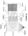
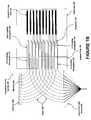


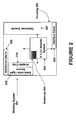
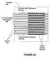


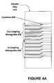

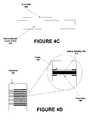

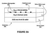


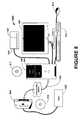


Classifications
- G—PHYSICS
- G01—MEASURING; TESTING
- G01N—INVESTIGATING OR ANALYSING MATERIALS BY DETERMINING THEIR CHEMICAL OR PHYSICAL PROPERTIES
- G01N21/00—Investigating or analysing materials by the use of optical means, i.e. using sub-millimetre waves, infrared, visible or ultraviolet light
- G01N21/62—Systems in which the material investigated is excited whereby it emits light or causes a change in wavelength of the incident light
- G01N21/63—Systems in which the material investigated is excited whereby it emits light or causes a change in wavelength of the incident light optically excited
- G01N21/64—Fluorescence; Phosphorescence
- G01N21/645—Specially adapted constructive features of fluorimeters
- G01N21/648—Specially adapted constructive features of fluorimeters using evanescent coupling or surface plasmon coupling for the excitation of fluorescence
- G—PHYSICS
- G01—MEASURING; TESTING
- G01N—INVESTIGATING OR ANALYSING MATERIALS BY DETERMINING THEIR CHEMICAL OR PHYSICAL PROPERTIES
- G01N21/00—Investigating or analysing materials by the use of optical means, i.e. using sub-millimetre waves, infrared, visible or ultraviolet light
- G01N21/75—Systems in which material is subjected to a chemical reaction, the progress or the result of the reaction being investigated
- G01N21/77—Systems in which material is subjected to a chemical reaction, the progress or the result of the reaction being investigated by observing the effect on a chemical indicator
- G01N21/7703—Systems in which material is subjected to a chemical reaction, the progress or the result of the reaction being investigated by observing the effect on a chemical indicator using reagent-clad optical fibres or optical waveguides
- G—PHYSICS
- G01—MEASURING; TESTING
- G01N—INVESTIGATING OR ANALYSING MATERIALS BY DETERMINING THEIR CHEMICAL OR PHYSICAL PROPERTIES
- G01N33/00—Investigating or analysing materials by specific methods not covered by groups G01N1/00 - G01N31/00
- G01N33/48—Biological material, e.g. blood, urine; Haemocytometers
- G01N33/50—Chemical analysis of biological material, e.g. blood, urine; Testing involving biospecific ligand binding methods; Immunological testing
- G01N33/53—Immunoassay; Biospecific binding assay; Materials therefor
- G01N33/543—Immunoassay; Biospecific binding assay; Materials therefor with an insoluble carrier for immobilising immunochemicals
- G01N33/54366—Apparatus specially adapted for solid-phase testing
- G01N33/54373—Apparatus specially adapted for solid-phase testing involving physiochemical end-point determination, e.g. wave-guides, FETS, gratings
- G—PHYSICS
- G01—MEASURING; TESTING
- G01N—INVESTIGATING OR ANALYSING MATERIALS BY DETERMINING THEIR CHEMICAL OR PHYSICAL PROPERTIES
- G01N2201/00—Features of devices classified in G01N21/00
- G01N2201/02—Mechanical
- G01N2201/024—Modular construction
- Y—GENERAL TAGGING OF NEW TECHNOLOGICAL DEVELOPMENTS; GENERAL TAGGING OF CROSS-SECTIONAL TECHNOLOGIES SPANNING OVER SEVERAL SECTIONS OF THE IPC; TECHNICAL SUBJECTS COVERED BY FORMER USPC CROSS-REFERENCE ART COLLECTIONS [XRACs] AND DIGESTS
- Y10—TECHNICAL SUBJECTS COVERED BY FORMER USPC
- Y10T—TECHNICAL SUBJECTS COVERED BY FORMER US CLASSIFICATION
- Y10T436/00—Chemistry: analytical and immunological testing
- Y10T436/14—Heterocyclic carbon compound [i.e., O, S, N, Se, Te, as only ring hetero atom]
- Y10T436/142222—Hetero-O [e.g., ascorbic acid, etc.]
- Y10T436/143333—Saccharide [e.g., DNA, etc.]
Definitions
- Biological substance analysis methods based on optical meanshave risen in popularity in the last couple of decades. Common to all these methods is that chemical interactions between the bio-molecules produce changes that affect some measurable optical properties, such as emission spectrum, absorption spectrum and index of refraction.
- microarray elementsare spotted on top of a flat substrate chip usually made of glass, plastic or epoxy. Subsequently, the chip is scanned using confocal scanning systems where the exciting light and the resulting fluorescence light are both shined and collected from above and analyzed using a single photo-multiplier (PMT) detector.
- PMTphoto-multiplier
- This arrangementsuffers from several inherent limitations including a very short interaction length between the bio-sample and the light (usually a single mono-layer). This limits the signal strength and thus the SNR.
- Another limitationis a high background or noise due to the fact that the back reflected light and the emitted fluorescent light travel in the same direction.
- a further limitationis high sensitivity to the planarity and the position of the chip that need to be maintained in focus.
- Still another limitationis slow operation due to the need to have large enough number of ‘pixels’ (scanned spots) within every sample and long enough integration time.
- Yet another limitationis the need for a complicated optical and mechanical structure that entails
- Another optical bio-analysis methodis waveguide based bio-sensors. Bio-sensing based on waveguides has been around for a while. These biosensors can be divided into three main categories. The first involve slab waveguide fluorescence excitation with light collection from above or below the chip. In this arrangement the bio-analyzed spots are located on the surface of a chip that contains a single slab-waveguide. Light is coupled into the waveguide using a lens or a grating that excites the entire chip with all its bio-analyzed spots simultaneously. The fluorescence is collected using an optical imaging system and a Charge-Coupled Device (CCD) detector from above or underneath the chip.
- CCDCharge-Coupled Device
- a second waveguide based bio-sensorutilizes an interferometric optical device.
- channel waveguidesare used together with interferometric devices such as Mach Zehender Interferometers (MZI) or ring-resonators.
- MZIMach Zehender Interferometers
- ring-resonatorsThese sensitive interferometric devices sense the change in the index of refraction due to binding of the bio-molecules near a waveguide surface.
- MZIMach Zehender Interferometers
- ring-resonatorsring-resonators.
- a third waveguide based bio-sensorutilizes Surface Plasmon Resonance (SPR).
- SPRSurface Plasmon Resonance
- a thin gold layer deposited on top of a glass substrateThe bio-analyzed sample on top of the gold induces changes in the refractive index above the gold layer and thus changing the resonant angle for generating surface Plasmons along the gold layer. The Plasmons generation is detected as an enhanced peak in the reflected beam. Examples of the SPR method are covered, for example, in U.S. Pat. No. 6,956,651 B2. Other types of optical bio-sensors and array scanners exist such as described in U.S. Pat. No. 6,396,995 B1.
- the inventionfeatures a scanning sensor system, methods and kits for use thereof including a light source, a detector, a substrate and a plurality of optical sensing sites.
- the substrateis in optical communication with the light source and the detector either directly or indirectly, for example, through an adapter chip.
- the substrateincludes a plurality of substantially parallel waveguides used both for guiding the excitation light to the sensing sites and for collecting the emitted light from the sensing sites.
- the plurality of optical sensing sitescan each be in optical communication with a waveguide.
- Implementations of the inventioncan include one or more of the following features.
- a scanning sensor system for detecting a biologically active analyteincluding a light source, a detector, a substrate comprising a plurality of waveguides and a plurality of optical sensing sites in optical communication with one or more waveguide of the substrate, and at least one adapter configured to couple with the substrate and provide optical communication between the light source, the waveguides of the substrate, and the detector.
- the substrate and the at least one adapterin some embodiments can be substantially planar and make up or comprise a planar lightwave circuit.
- the at least one adaptercan be further configured to removably couple with the substrate.
- the at least one adaptercan be further coupled to at least one of the light source and the detector.
- the at least one adaptercan in one embodiment be a single adapter further coupled to the light source and the detector.
- Coupling of the system componentscan be by fiber optic.
- the adapterin some embodiments includes a plurality of edges and coupling of the adapter to the light source and the detector includes coupling to a first edge of the adapter and coupling to the substrate comprises coupling at a second edge of the adapter.
- the plurality of waveguides of the substrate and/or the adaptercan include in-coupling waveguides and out-coupling waveguides.
- the in-coupling waveguidescan be coupled to the out-coupling waveguides through a combiner.
- the substratefurther includes at least one combiner.
- the adapterfurther includes at least one combiner.
- the at least one adapteris a single adapter
- the plurality of waveguidesinclude in-coupling waveguides and out-coupling waveguides, wherein the in-coupling waveguides are coupled to the out-coupling waveguides through a combiner
- the light sourcecomprises a light generator element coupled to at least one in-coupling waveguide
- the detectorincludes a detector element coupled to at least one out-coupling waveguide.
- the optical sensing sitecan include a sensor configured to transduce a first light wave generated by the light source in a waveguide, resulting in a second light wave in the same waveguide, the second light wave being detectable by the detector.
- the plurality of waveguidescan be in-coupling waveguides coupled to out-coupling waveguides by way of combiners, and a first light wave can be carried by an in-coupling waveguide and a second light wave can be carried by an out-coupling waveguide.
- the adapter and substrateinclude inter-coupling optically communicating in-coupling waveguides and out-coupling waveguides and the substrate further includes the combiners.
- the sensorcan include a biologically active analyte in a sample, and wherein a measurable change in a first light wave results when the sensor discriminates or interacts with the biologically active analyte.
- the sensoris adapted to support an immunoassay.
- the immunoassay supportedcan be an enzyme-linked immunosorbent assay (ELISA).
- the immunoassay supportedcan be a fluorescent immunoassay.
- the sensorcan be selected from the group including a fluorescence well, an absorption cell, an interferometric sensor, a diffractive sensor and surface plasmon resonance sensor.
- the biologically active analytecan be selected from the group including a nucleic acid, a protein, an antigen, an antibody, a microorganism, a gas, a chemical agent and a pollutant.
- the nucleic acidis produced via an amplification reaction.
- the waveguidescan be single-mode.
- the waveguidescan alternatively be multi-mode.
- the waveguidesare single-mode in the vertical dimension and multi-mode in the lateral dimension.
- the optical sensing sitescan include wells. In one embodiment the optical sensing sites include the surface of the substrate above the waveguides, In another embodiment the optical sensing sites include biochemical interaction sites. In a further embodiment the optical sensing sites include optical transducers.
- the optical transducerscan include fluorescence wells comprising fluorescent or luminescent compounds, wherein light waves guided by a waveguide of the plurality of waveguides excite the fluorescent or luminescent compound in the wells in the presence of a biologically active analyte, and the same waveguide collects and guides light emitted from the wells to the detector.
- the number of optical sensing sitescan be greater than 10, greater than 200, or greater than 5,000.
- the light sourcecan be switchable or passive.
- the light sourceincludes a dynamic light source.
- the light sourceis a passive 1 ⁇ N splitter with N being between 1 and 1000.
- the light sourcecan include a chip containing an array of light generators coupled to an array of waveguides.
- the light sourceis an optical switch including a light generator coupled to one or more input of the optical switch.
- the optical switchfurther includes a branched architecture.
- the optical switchcan further include one or more inputs and multiple outputs.
- the optical switchcan further include greater than about 10 outputs, greater than about 100 outputs or greater than about 1,000 outputs. In one embodiment the optical switch further includes substantially between 20 and 200 outputs.
- the light generatorcan provide variable wavelengths of light.
- the light generatorcan be selected from the group including a broad-band source, a source with one or more discrete spectral lines and a tunable source.
- the light sourcecan be butt-coupled to one or more of the at least one adapter.
- the light sourceincludes one or more waveguide and is evanescently coupled to the at least one adapter through a proximate arrangement of the one or more light source waveguide and one or more waveguide of the at least one adapter.
- the detectorcan be a photodetector array.
- the detectoris a plurality of detectors.
- two or more detectorsare coupled to and in optical communication with one or more waveguide of the at least one adapter at one or more edges of the at least one adapter.
- the systemcan further include a thermal transfer element in thermal communication with the substrate.
- the thermal transfer elementis a thermoelectric cooler.
- each optical sensing siteincludes a thermal transfer element in thermal communication with the optical sensing site.
- the thermal transfer elementcan include a thin-film heater.
- each optical sensing sitefurther includes a thermistor in thermal communication with the optical sensing site.
- the substratecan further include one or more microchannel and one or more reservoirs in fluid communication with one or more optical sensing site.
- the systemfurther includes a fluidics layer coupled to the substrate and includes one or more microchannel and one or more reservoirs in fluid communication with one or more optical sensing site.
- a scanning sensing methodincluding coupling a removable substrate including a plurality of in-coupling waveguides, a plurality of out-coupling waveguides and combiners for coupling the in-coupling and out-coupling waveguides, wherein the substrate is coupled in optical communication with an adapter, a light source, and a detector to provide a scanning sensor system, wherein the adapter is coupled to the light source and the detector.
- the methodfurther includes delivering a sample suspected of containing a biologically active analyte to be detected to an optical sensing site of the substrate, providing a first light wave using a light source to one or more of the plurality of in-coupling waveguides of the substrate, wherein the in-coupling waveguides are in optical communication with the optical sensing site, wherein the first light wave is transducable by a sensor associated with the optical sensing site to a second light wave carried to an out-coupling waveguide, and detecting a measurable change in the second light wave using the detector, wherein a measurable change in the first light waves occurs when the sensor interacts with the biologically active analyte.
- Scanning sensingcan further include switching one or more input light wave from the light source into the substrate to produce the first light wave in one or more of the in-coupling waveguides.
- the light sourceincludes an optical switch for controlled switching of one or more input light wave, the optical switch can multicast light to a plurality of outputs and into the substrate to controllably produce the first light wave in one or more of the in-coupling waveguides.
- the light sourcecan include an array of individually controlled light generators for controlled switching of one or more input light wave, to controllably produce the first light wave in one or more of the in-coupling waveguides.
- the methodcan further include simultaneously detecting the second light wave with the detector wherein the detector comprises a photodetector array.
- a portion of the sensing sitesinclude reference sample material for calibration and/or normalization.
- the biologically active analytecan be selected from the group consisting of a nucleic acid, a protein, an antigen, an antibody, a microorganism, a gas, a chemical agent and a pollutant.
- the biologically active analyteis a protein.
- a single nucleotide polymorphism (SNP)is detected in the biologically active analyte.
- expression of a geneis detected upon detection of the biologically active analyte.
- the sensorcan be adapted to support an immunoassay and wherein the sensor interacting with the biologically active analyte includes an outcome of an immunoassay.
- the immunoassay supportedis an enzyme-linked immunosorbent assay (ELISA).
- the immunoassay supportedcan be a fluorescent immunoassay.
- Detecting a measurable change in the second lightwavecan provide a diagnostic result.
- the methodcan further include conducting a real-time PCR reaction at the optical sensing site.
- a kit for assaying a sample for a biologically active analyteincluding a scanning sensor system including a light source, a detector, a substrate comprising a plurality of waveguides and a plurality of optical sensing sites in optical communication with one or more waveguide of the substrate, and at least one adapter configured to couple with the substrate and provide optical communication between the light source, the waveguides of the substrate, and the detector.
- the kitfurther includes packaging and instructions for use of the system.
- the adapter and substrateincludes a planar lightwave circuit.
- the optical sensing sitesincludes a sensor adapted to support an immunoassay, and wherein the kit further includes one or more immunoassay reagents.
- FIG. 1Ais a schematic of the scanning sensing system according to one embodiment of the invention including a switchable light source, fibers, an adapter chip, a substrate, optical sensing sites and a detector.
- FIG. 1Bis a schematic of the scanning sensing system according to another embodiment of the invention including a switchable light source, fibers, an adapter chip, a substrate, optical sensing sites and a detector.
- FIG. 1Cis a schematic of the scanning sensing system according to another embodiment of the invention a including a switchable light source, fibers, two adapter chips, a substrate, optical sensing sites and a detector.
- FIG. 1Dis a schematic of the scanning sensing system according to another embodiment of the invention including a switchable light source and detector chip, a substrate, and optical sensing sites.
- FIG. 2is block diagram showing the scanning system of the invention in a housing as part of a working system.
- FIG. 3Ais a schematic of the substrate of the invention according to one embodiment including optical waveguides in conjunction with optical sensing sites and barriers.
- FIG. 3Bis a schematic of the substrate of the invention according to another embodiment including optical waveguides and combiners in conjunction with optical sensing sites and barriers.
- FIG. 3Cis a schematic cross section of the substrate of the invention according to one embodiment including an optical waveguide in conjunction with an optical sensing site.
- FIG. 4Ais a schematic of the adapter chip of the invention according to one embodiment including optical in-coupling and out-coupling waveguides and the optical combiners.
- FIG. 4Bis a schematic of the adapter chip of the invention according to the second embodiment including the optical in-coupling and out-coupling waveguides.
- FIG. 4Cis a schematic of a side view of the substrate in relation to a thermoelectric cooler.
- FIG. 4Dis a schematic of the substrate of the invention illustrating details of an optical sensing site including a heater and a thermistor.
- FIG. 4Eis a schematic of the substrate of the invention including reservoirs and micro channels in relation to optical sensing sites.
- FIG. 5Ais a schematic of a general substrate including typical layers and waveguides representative of those of the current invention.
- FIG. 5Bis a photomicrograph image of waveguides representative of those of the invention and a silica layer.
- FIG. 5Cis a perspective view of waveguides and associated substrate layers.
- FIG. 6Ais a schematic of a switchable light source of the invention including inputs and outputs.
- FIG. 6Bis a schematic of a branched architecture between the inputs and outputs of a switchable light source of the invention.
- FIG. 6Cis a schematic of one embodiment of a switchable light source and detector chip of the invention including light generator elements, detector elements, in-coupling and out-coupling waveguides and combiners.
- FIG. 7is a schematic of a detector of the invention.
- FIG. 8is a block diagram showing a representative example logic device in communication with an apparatus for use with the scanning sensing system of the invention.
- FIG. 9is a block diagram showing a representative example of a kit.
- FIGS. 10A-Dare schematics illustrating a representative manufacturing process for the substrate and waveguides of the invention.
- FIG. 11is a flow chart showing a representative manufacturing process for the substrate.
- Apparatus, methods, and kits for optical sensing, using a scanning sensing system including a light source, a detector, at least one adapter, a substrate and a plurality of optical sensing sitesare provided.
- Related scanning sensing systems, methods and kits including such systemshave been previously described in U.S. patent application Ser. No. 11/683,808 filed Mar. 8, 2007, the entire contents of which are incorporated herein by reference.
- the substrate of the present systemincludes a plurality of substantially parallel waveguides and a plurality of sensing sites.
- the at least one adapter of the systemcan provide for removable coupling of the substrate with system components.
- the optical sensing sitesinclude a sensor and are in optical communication with one or more waveguides. Sensing of a variety of environmental and biological samples can be achieved using the apparatus, methods and kits described herein. The general theoretical principles of lightwave guiding and evanescent field fluorescence excitation apply to the embodiments disclosed herein.
- a biologically active analytecan be any substance which can affect any physical or biochemical properties of a biological organism, including but not limited to viruses, bacteria, fungi, plants, animals, and humans.
- biologically active analyte according to the present inventionincludes without limitation drugs, prodrugs, pharmaceutical agents, drug metabolites, biomarkers such as expressed proteins and cell markers, antibodies, serum proteins, cholesterol, polysaccharides, nucleic acids, biological analytes, gene, protein, or hormone, or any combination thereof.
- a biologically active analytecan further include a natural or man-made substance including but not limited to a gas, a chemical agent or a pollutant, or a combination thereof (e.g., from an environmental source).
- the biologically active analytescan be polypeptide glycoprotein, polysaccharide, lipid, nucleic acid, and a combination thereof.
- biomarkers associated with a particular disease or with a specific disease stageare biomarkers associated with a particular disease or with a specific disease stage.
- Such biologically active analytesinclude but are not limited to those associated with autoimmune diseases, obesity, hypertension, diabetes, neuronal and/or muscular degenerative diseases, cardiac diseases, endocrine disorders, any combinations thereof.
- biomarkersthat are present in varying abundance in one or more of the body tissues including heart, liver, prostate, lung, kidney, bone marrow, blood, skin, bladder, brain, muscles, nerves, and selected tissues that are affected by various disease, such as different types of cancer (malignant or non-metastatic), autoimmune diseases, inflammatory or degenerative diseases.
- body tissuesincluding heart, liver, prostate, lung, kidney, bone marrow, blood, skin, bladder, brain, muscles, nerves, and selected tissues that are affected by various disease, such as different types of cancer (malignant or non-metastatic), autoimmune diseases, inflammatory or degenerative diseases.
- biologically active analytesthat are indicative of a microorganism.
- exemplary microorganismsinclude but are not limited to bacterium virus, fungus and protozoa.
- Biologically active analytes that can be detected by the subject methodalso include blood-born pathogens selected from a non-limiting group that consists of Staphylococcus epidermidis, Escherichia coli , methicillin-resistant Staphylococcus aureus (MSRA),
- Staphylococcus aureusStaphylococcus hominis, Enterococcus faecalis, Pseudomonas aeruginosa, Staphylococcus capitis, Staphylococcus warneri, Klebsiella pneumoniae, Haemophilus influnzae, Staphylococcus simulans, Streptococcus pneumoniae and Candida albicans.
- Biologically active analytes that can be detected by the subject device and methodsalso encompass a variety of sexually transmitted diseases selected from the following: gonorrhea ( Neisseria gorrhoeae ), syphilis ( Treponena pallidum ), chlamydia ( Chlamydia tracomitis ), nongonococcal urethritis ( Ureaplasma urealyticum ), yeast infection
- Candida albicansCandida albicans
- chancroidHaemophilus ducreyi
- trichomoniasisTrichomonas vaginalis
- genital herpesHSV type I and II
- HIV IHIV II
- hepatitis A, B, C, Gas well as hepatitis caused by TTV.
- Additional biologically active analytesthat can be detected by the subject apparatus and methods encompass a diversity of respiratory pathogens including but not limited to Pseudomonas aeruginosa , methicillin-resistant
- Staphylococcus aureus(MSRA), Klebsiella pneumoniae, Haemophilis influenzae, Staphylococcus aureus, Stenotrophomonas maltophilia, Haemophilis parainfluenzae, Escherichia coli, Enterococcus faecalis, Serratia marcescens, Haemophilis parahaemolyticus, Enterococcus cloacae, Candida albicans, Moraxiella catarrhalis,
- Streptococcus pneumoniaeCitrobacter freundii, Enterococcus faeciurn, Klebsiella oxytoca, Pseudomonas fluorsecens, Neisseria meningitidis, Streptococcus pyogenes, Pneumocystis carinii, Klebsiella pneumoniae, Legionella pneumophila, Mycoplasma pneumoniae , and Mycobacterium tuberculosis.
- TheophyllineCRP, CKMB, PSA, Myoglobin, CA125, Progesterone, TxB2, 6-keto-PGF-1-alpha, and Theophylline, Estradiol, Lutenizing hormone, High sensitivity CRP, Triglycerides, Tryptase, Low density lipoprotein Cholesterol, High density lipoprotein Cholesterol, Cholesterol, IGFR.
- liver markersinclude without limitation LDH, (LD5), (ALT), Arginase 1 (liver type), Alphafetoprotein (AFP), Alkaline phosphatase, Alanine aminotransferase, Lactate dehydrogenase, and Bilirubin.
- kidney markersinclude without limitation TNFa Receptor, Cystatin C, Lipocalin-type urinary prostaglandin D, synthatase (LPGDS), Hepatocyte growth factor receptor, Polycystin 2, Polycystin 1, Fibrocystin, Uromodulin, Alanine, aminopeptidase, N-acetyl-B-D-glucosaminidase, Albumin, and Retinol-binding protein (RBP).
- Exemplary heart markersinclude without limitation Troponin I (TnI), Troponin T (TnT), CK, CKMB, Myoglobin, Fatty acid binding protein (FABP), CRP, D-dimer, S-100 protein, BNP, NT-proBNP, PAPP-A, Myeloperoxidase (MPO), Glycogen phosphorylase isoenzyme BB (GPBB), Thrombin Activatable Fibrinolysis Inhibitor (TAFI), Fibrinogen, Ischemia modified albumin (IMA), Cardiotrophin-1, and MLC-I (Myosin Light Chain-I).
- TnITroponin I
- TnTTroponin T
- CKTroponin T
- CKMBMyoglobin
- CRPD-dimer
- S-100 proteinS-100 protein
- BNPBNP
- NT-proBNPNT-proBNP
- PAPP-AMyeloperoxidas
- pancreas markersinclude without limitation Amylase, Pancreatitis-Associated protein (PAP-1), and Regeneratein proteins (REG).
- PAP-1Pancreatitis-Associated protein
- REGRegeneratein proteins
- Exemplary muscle tissue markersinclude without limitation Myostatin.
- Exemplary blood markersinclude without limitation Erythopoeitin (EPO).
- EPOErythopoeitin
- Exemplary bone markersinclude without limitation, Cross-linked N-telopeptides of bone type I collagen (NTx), Carboxyterminal cross-linking telopeptide of bone collagen, Lysyl-pyridinoline (deoxypyridinoline), Pyridinoline, Tartrate-resistant acid phosphatase, Procollagen type I C propeptide, Procollagen type I N propeptide, Osteocalcin (bone gla-protein), Alkaline phosphatase, Cathepsin K, COMP (Cartilage Oligomeric Matrix Protein), Osteocrin, Osteoprotegerin (OPG), RANKL, sRANK, TRAP 5 (TRACP 5), Osteoblast Specific Factor 1 (OSF-1, Pleiotrophin), Soluble cell adhesion molecules, sTfR, sCD4, sCD8, sCD44, and Osteoblast Specific Factor 2 (OSF 2, Periostin).
- NTxCross-linked N
- markers according to the present inventionare disease specific.
- Exemplary cancer markersinclude without limitation PSA (total prostate specific antigen), Creatinine, Prostatic acid phosphatase, PSA complexes, Prostrate-specific gene-1, CA 12-5, Carcinoembryonic Antigen (CEA), Alpha feto protein (AFP), hCG (Human chorionic gonadotropin), Inhibin, CAA Ovarian C1824, CA 27.29, CA 15-3, CAA Breast C1924, Her-2, Pancreatic, CA 19-9, Carcinoembryonic Antigen, CAA pancreatic, Neuron-specific enolase, Angiostatin.
- PSAtotal prostate specific antigen
- CreatinineProstatic acid phosphatase
- PSA complexesProstrate-specific gene-1
- CA 12-5Carcinoembryonic Antigen
- CEACarcinoembryonic Antigen
- AFPAlpha feto protein
- hCGHuman chorionic gonadotropin
- DcR3Soluble decoy receptor 3
- EndostatinEp-CAM (MK-1), Free Immunoglobulin Light Chain Kappa, Free Immunoglobulin Light Chain Lambda, Herstatin, Chromogranin A, Adrenomedullin, Integrin, Epidermal growth factor receptor, Epidermal growth factor receptor-Tyrosine kinase, Pro-adrenomedullin N-terminal 20 peptide, Vascular endothelial growth factor, Vascular endothelial growth factor receptor, Stem cell factor receptor, c kit/KDR, KDR, and Midkine.
- infectious disease markersinclude without limitation Viremia, Bacteremia, Sepsis, PMN Elastase, PMN elastase/ ⁇ 1-PI complex, Surfactant Protein D (SP-D), HBVc antigen, HBVs antigen, Anti-HBVc, Anti-HIV, Tsuppressor cell antigen, T-cell antigen ratio, T-helper cell antigen, Anti-HCV, Pyrogens, p24 antigen, Muramyldipeptide.
- SP-DSurfactant Protein D
- HBVc antigenHBVs antigen
- Anti-HBVcAnti-HIV
- Tsuppressor cell antigenT-cell antigen ratio
- T-helper cell antigenAnti-HCV
- PyrogensPyrogens
- p24 antigenMuramyldipeptide.
- Exemplary diabetes markersinclude without limitation C-Peptide, Hemoglobin A1c, Glycated albumin, Advanced glycosylation end products (AGEs), 1,5-anhydroglucitol, Gastric Inhibitory Polypeptide, Glucose, Hemoglobin, ANGPTL3 and 4.
- Exemplary inflammation markersinclude without limitation Rheumatoid factor (RF), Antinuclear Antibody (ANA), C-reactive protein (CRP), Clara Cell Protein (Uteroglobin).
- RFRheumatoid factor
- ANAAntinuclear Antibody
- CRPC-reactive protein
- Clara Cell ProteinUteroglobin
- Exemplary allergy markersinclude without limitation Total IgE and Specific IgE.
- autism markersinclude without limitation Ceruloplasmin, Metalothioneine, Zinc, Copper, B6, B12, Glutathione, Alkaline phosphatase, and Activation of apo-alkaline phosphatase.
- Exemplary coagulation disorders markersinclude without limitation b-Thromboglobulin, Platelet factor 4, Von Willebrand factor.
- a markermay be therapy specific.
- COX inhibitorsinclude without limitation TxB2 (Cox-1), 6-keto-PGF-1-alpha (Cox 2), 11-Dehydro-TxB-1a (Cox-1).
- markers of the presentinclude without limitation Leptin, Leptin receptor, and Procalcitonin, Brain S100 protein, Substance P, 8-Iso-PGF-2a.
- Exemplary geriatric markersinclude without limitation, Neuron-specific enolase, GFAP, and S100B.
- Exemplary markers of nutritional statusinclude without limitation Prealbumin, Albumin, Retinol-binding protein (RBP), Transferrin, Acylation-Stimulating Protein (ASP), Adiponectin, Agouti-Related Protein (AgRP), Angiopoietin-like Protein 4 (ANGPTL4, FIAF), C-peptide, AFABP (Adipocyte Fatty Acid Binding Protein, FABP4), Acylation-Stimulating Protein (ASP), EFABP (Epidermal Fatty Acid Binding Protein, FABP5), Glicentin, Glucagon, Glucagon-Like Peptide-1, Glucagon-Like Peptide-2, Ghrelin, Insulin, Leptin, Leptin Receptor, PYY, RELMs, Resistin, and sTfR (soluble Transferrin Receptor).
- Exemplary markers of Lipid metabolisminclude without limitation Apo-lipoproteins (several), Apo-A1, Apo-B, Apo-C-CII, Apo-D, Apo-E.
- Exemplary coagulation status markersinclude without limitation Factor I: Fibrinogen, Factor II: Prothrombin, Factor III: Tissue factor, Factor IV: Calcium, Factor V: Proaccelerin, Factor VI, Factor VII: Proconvertin, Factor VIII: Anti-hemolytic factor, Factor IX: Christmas factor, Factor X: Stuart-Prower factor, Factor XI: Plasma thromboplastin antecedent, Factor XII: Hageman factor, Factor XIII: Fibrin-stabilizing factor, Prekallikrein, High molecular-weight kininogen, Protein C, Protein S, D-dimer, Tissue plasminogen activator, Plasminogen, a2 Antiplasmin, Plasminogen activator inhibitor 1 (PAI1).
- Factor IFibrinogen
- Factor IIProthrombin
- Factor IIITissue factor
- Factor IVCalcium
- Factor VProaccelerin
- Exemplary monoclonal antibody markersinclude those for EGFR, ErbB2, and IGF1R.
- Exemplary tyrosine kinase inhibitor markersinclude without limitation Ab1, Kit, PDGFR, Src, ErbB2, ErbB 4, EGFR, EphB, VEGFR1-4, PDGFRb, FLt3, FGFR, PKC, Met, Tie2, RAF, and TrkA.
- Exemplary Serine/Threonine Kinase Inhibitor markersinclude without limitation AKT, Aurora A/BIB, CDK, CDK (pan), CDK1-2, VEGFR2, PDGFRb, CDK4/6, MEK1-2, mTOR, and PKC-beta.
- GPCR target markersinclude without limitation Histamine Receptors, Serotonin Receptors, Angiotensin Receptors, Adrenoreceptors, Muscarinic Acetylcholine Receptors, GnRH Receptors, Dopamine Receptors, Prostaglandin Receptors, and ADP Receptors.
- a therapeutic agentcan be any substances that have therapeutic utility and/or potential. Such substances include but are not limited to biological or chemical compounds such as a simple or complex organic or inorganic molecules, peptides, proteins (e.g. antibodies) or a polynucleotides (e.g. anti-sense). Other therapeutic agents include a vast array of compounds that can be synthesized, for example, polymers, such as polypeptides and polynucleotides, and synthetic organic compounds based on various core structures. In addition, various natural sources can provide compounds for screening, such as plant or animal extracts, and the like. It should be understood, although not always explicitly stated that the agent is used alone or in combination with another agent, having the same or different biological activity as the agents identified by the inventive screen. The agents and methods also are intended to be combined with other therapies.
- Pharmacodynamic (PD) parametersinclude without limitation physical parameters such as temperature, heart rate/pulse, blood pressure, and respiratory rate, and biomarkers such as proteins, cells, and cell markers. Biomarkers could be indicative of disease or could be a result of the action of a drug.
- Pharmacokinetic (PK) parameters according to the present inventioninclude without limitation drug and drug metabolite concentration. Identifying and quantifying the PK parameters rapidly from a sample volume is extremely desirable for proper safety and efficacy of drugs. If the drug and metabolite concentrations are outside a desired range and/or unexpected metabolites are generated due to an unexpected reaction to the drug, immediate action may be necessary to ensure the safety of the patient. Similarly, if any of the PD parameters fall outside the desired range during a treatment regime, immediate action may have to be taken as well.
- physical parameter datais stored in or compared to stored profiles of physical parameter data in a bioinformatics system which may be on an external device incorporating pharmacogenomic and pharmacokinetic data into its models for the determination of toxicity and dosing. Not only does this generate data for clinical trials years prior to current processes but also enables the elimination of current disparities between apparent efficacy and actual toxicity of drugs through real-time continuous monitoring. During the go/no go decision process in clinical studies, large scale comparative population studies can be conducted with the data stored on the database. This compilation of data and real-time monitoring allows more patients to enter clinical trials in a safe fashion earlier than currently allowed.
- biomarkers discovered in human tissue studiescan be targeted by the scanning sensing system for improved accuracy in determining drug pathways and efficacy in cancer studies.
- a nucleic acidcan be deoxyribonucleotides, deoxyribonucleosides, ribonucleosides or ribonucleotides and polymers thereof in either single- or double-stranded form.
- Nucleic acidsmay contain known analogues of natural nucleotides which have similar binding properties as the reference nucleic acid and are metabolized in a manner similar to naturally occurring nucleotides.
- Nucleic acidsmay also include oligonucleotide analogs including PNA (peptidonucleic acid), analogs of DNA used in antisense technology (phosphorothioates, phosphoroamidates, and the like).
- nucleic acid sequencealso implicitly encompasses conservatively modified variants thereof (including but not limited to, degenerate codon substitutions) and complementary sequences as well as the sequence explicitly indicated.
- degenerate codon substitutionsmay be achieved by generating sequences in which the third position of one or more selected (or all) codons is substituted with mixed-base and/or deoxyinosine residues (Batzer et al., Nucleic Acid Res. 19:5081 (1991); Ohtsuka et al., J. Biol. Chem. 260:2605-2608 (1985); and Rossolini et al., Mol. Cell. Probes 8:91-98 (1994)).
- Microorganismcan include but is not limited to bacteria, actinomycetales, cyanobacteria (unicellular algae), fingi, protozoa, animal cells or plant cells or virus. Examples of microorganisms include but are not limited to pathogens.
- polypeptiderefers to a polymer of amino acid residues. That is, a description directed to a polypeptide applies equally to a description of a peptide and a description of a protein, and vice versa.
- the termsapply to naturally occurring amino acid polymers as well as amino acid polymers in which one or more amino acid residues is a non-natural amino acid.
- the termsencompass amino acid chains of any length, including full length proteins (i.e., antigens), wherein the amino acid residues are linked by covalent peptide bonds.
- proteins that contain multiple polypeptide chains that associate through covalent and/or non-covalent interactionsare also encompassed by “protein,” as used herein.
- a polymorphismis the occurrence of two or more genetically determined alternative sequences or alleles in a population.
- a polymorphic marker or siteis the locus at which divergence occurs. Preferred markers have at least two alleles, each occurring at frequency of greater than 1%, and more preferably greater than 10% or 20% of a selected population.
- a polymorphismmay comprise one or more base changes, an insertion, a repeat, or a deletion.
- a polymorphic locusmay be as small as one base pair.
- Polymorphic markersinclude restriction fragment length polymorphisms, variable number of tandem repeats (VNTR's), hypervariable regions, minisatellites, dinucleotide repeats, trinucleotide repeats, tetranucleotide repeats, simple sequence repeats, and insertion elements such as Alu.
- the first identified allelic formis arbitrarily designated as the reference form and other allelic forms are designated as alternative or variant alleles.
- the allelic form occurring most frequently in a selected populationis sometimes referred to as the wildtype form. Diploid organisms may be homozygous or heterozygous for allelic forms.
- a dialelic polymorphismhas two forms.
- a triallelic polymorphismhas three forms.
- a single nucleotide polymorphismoccurs at a polymorphic site occupied by a single nucleotide, which is the site of variation between allelic sequences.
- the siteis usually preceded by and followed by highly conserved sequences of the allele (e.g., sequences that vary in less than 1/100 or 1/1000 members of the populations).
- a single nucleotide polymorphismusually arises due to substitution of one nucleotide for another at the polymorphic site.
- a transitionis the replacement of one purine by another purine or one pyrimidine by another pyrimidine.
- a transversionis the replacement of a purine by a pyrimidine or vice versa.
- Single nucleotide polymorphismscan also arise from a deletion of a nucleotide or an insertion of a nucleotide relative to a reference allele.
- An individualincludes but is not limited to a human being, but may also include other organisms including but not limited to mammals, plants, bacteria or cells derived from any of the above.
- aspects of the inventionmay include one or more of the following advantageous features. Dense and accurate integration of optical manipulating elements can be achieved using planar lightwave circuits technology. Applications for planar lightwave circuits as described herein include new drag discovery and development, disease research, biomarkers discovery, SNP association studies including toxicology and disease susceptibility, and diagnostics including identifying patients predisposed to diseases and identifying patients with particular drug sensitivity.
- FIG. 1Aillustrates an exemplary scanning sensing system 100 of the invention including a switchable light source 102 , an adapter chip 114 , a substrate 104 , optical sensing sites 112 and a detector 106 .
- a switchable light sourceis illustrated in the accompanying figures, it is envisioned that the light source can be any of a number of types of light sources including but not limited to switchable light sources or passive light sources.
- Adapter chip 114can include in-coupling waveguides 128 , out-coupling waveguides 126 and combiners 130 which combine the in-coupling and the out-coupling waveguides. Such combiners 130 are well known in the art.
- Substrate 104can include waveguides 108 and sensing sites 112 in relation to waveguides 108 .
- sensing sites 112can be on top of and in optical communication with waveguides 108 .
- Detector 106can include one or more element 116 .
- switchable light source 102is coupled to and is in optical communication with in-coupling waveguides 128 on adapter chip 114 through optical fibers 118 .
- Optical fibers 118can be a set of optical fibers as shown in FIG. 1A .
- detector 106can be coupled to and in optical communication with out-coupling waveguides 126 on adapter chip 114 , for example, through a second set of optical fibers 118 .
- Adapter chip 114can further be coupled and in optical communication with one or more of waveguides 108 at a first edge of substrate 104 .
- Adapter chip 114 of this embodiment and all other embodimentscan optionally be configured to provide removable coupling for substrate 104 or other system components described herein.
- substrate 104can further be configured to provide removable coupling with adapter chip 114 or other components of the system.
- FIG. 1Billustrates an exemplary scanning sensing system 100 of the invention including a switchable light source 102 , an adapter chip 114 , a substrate 104 , optical sensing sites 112 and a detector 106 .
- Adapter chip 114can include in-coupling waveguides 128 and out-coupling waveguides 126 .
- Substrate 104can include in-coupling waveguides 110 , out-coupling waveguides 108 , combiners 132 which combine in-coupling 110 and out-coupling waveguides 108 and sensing sites 112 , for example on top of and in optical communication with out-coupling waveguides 108 .
- Detector 106can include one or more element 116 as described herein.
- switchable light source 102is coupled to and is in optical communication with in-coupling waveguides 128 of adapter chip 114 through a set of optical fibers 118 .
- detector 106is coupled to and in optical communication with out-coupling waveguides 126 of adapter chip 114 through a second set of optical fibers 118 .
- Adapter chip 114is further coupled to and in optical communication with one or more in-coupling waveguides 110 and with one or more of out-coupling waveguides 108 , for example, at an edge of substrate 104 .
- FIG. 1Cillustrates an exemplary scanning sensing system 100 of the invention including a switchable light source 102 , two adapter chips 114 , a substrate 104 , optical sensing sites 112 and a detector 106 .
- the adapter chipsinclude waveguides 134 .
- the substrateincludes waveguides 108 and sensing sites 112 on top of and in optical communication with the waveguides.
- the switchable light source 102is coupled to and is in optical communication with waveguides 134 on one adapter chip 114 through a set of optical fibers 118 .
- detector 106is coupled to and in optical communication with waveguides 134 on a second adapter chip 114 through a second set of optical fibers 118 .
- the two adapter chips 114are further coupled and in optical communication with one or more of waveguides 108 at two opposite edges of the substrate 104 .
- detector 106can include one or more elements 116 .
- FIG. 1Dillustrates an exemplary scanning sensing system 100 of the invention including a combined switchable light source and detector chip 120 , a substrate 104 and optical sensing sites 112 .
- the combined switchable light source and detector chip 120includes light generator elements 122 , detector elements 124 , combiners 136 , out-coupling waveguides 138 and in-coupling waveguides 140 .
- Substrate 104includes waveguides 108 and optical sensing sites 112 that can be arranged, for example, on top of and in optical communication with waveguides 108 .
- light generator elements 122are coupled to and in optical communication with in-coupling waveguides 140 .
- detector elements 124are coupled to and in optical communication with out-coupling waveguides 138 on the combined switchable light source and detector chip 120 .
- Switchable light source and detector chip 120is further coupled to and in optical communication with one or more waveguides 108 at an edge of substrate 104 .
- a first switchable light source and detector chipis coupled to a first edge of the substrate and a second switchable light source and detector chip is coupled at a second edge of the substrate (not shown). It can be understood accordingly that the passage of light waves within the devices and systems described herein, though described in terms of “left” and “right” can be practiced in a variety of directions and orientations based on the flexible arrangements of components provided herein.
- system 100can be substantially planar.
- switchable light source 102can be a planar chip.
- This chipcan be coupled to a planar adapter chip 114 that is a second chip, that is further coupled to a planar substrate 104 that is a third chip.
- system 100is a planar lightwave circuit including three or more coupled planar chips.
- two chipsare integrated into a single chip (e.g., in the switchable light source and detector chip or in an adapter chip and substrate chip). Such a configuration would be useful in a case where the substrate chip is reusable and can be effectively used for long periods of time.
- One application of such a configurationwould be in a system for detecting biological warfare-associated agents. In such an application it would be advantageous for the system to operate for long periods of time without a need for replacing the chip.
- having two chips integrated on a single substratesolves the problem of maintaining the relative alignment of two chips (e.g., an adapter chip and substrate chip).
- the substratecan be a multi-element bio-analysis chip.
- an optical sensing site 112can be associated with each waveguide 108 . It is envisioned that the number of optical sensing sites on a substrate chip can be greater than 10, greater than 100, greater than 200, greater than 1,000, great than 5,000 or greater than 10,000. It is further envisioned that the density of optical sensing sites can be greater than 10 per cm 2 , greater than 100 per cm 2 , greater than 1,000 per cm 2 or greater than 10,000 per cm 2 . In one embodiment the density of optical sensing sites is greater than 2,000 per cm 2 .
- a first light wave generated by the switchable light source in an in-coupling waveguideinduces the sensor to transduce an optical signal resulting in a second light wave in an out-coupling waveguide, the second light wave being detectable by the detector.
- System 100is a planar two-dimensional scanning system.
- System 100 in this embodimentincludes a planar switchable light source 102 , for example, a planar optical switch or an array of switchable lasers, coupled to the plane of substrate 104 through a planar adapter chip 114 , to make up, for example, a bioanalysis chip plane.
- switchable light source 102can provide a dynamic source of light for selective and programmed excitation in respect to individual waveguides 108 , providing excitation to part or to all of optical sensing sites 112 .
- a dynamic light sourceincludes but is not limited to a tunable wavelength and/or tunable bandwidth light source.
- system 100 of this embodimentprovides for planar collection of the emitted light from all the excited sensing sites 112 in out-coupling waveguides 108 , specifically in the plane of substrate 104 , such that the light collection is in substantially opposite direction to the light produced in in-coupling waveguides 110 .
- FIG. 2is an exemplary illustration of the scanning system of the invention as part of a working system 201 in a housing 209 . While the scanning sensing system illustrated in FIG. 1A-1D is core of the present invention, in order to facilitate the operation of this system, one or more other modules can be included in a working system that includes the scanning sensing system components of the invention.
- FIG. 2illustrates one possible configuration for a working system 201 that can include housing 209 for enclosing various modules of working system 201 including but not limited to substrate 204 , robotic system 203 , switchable light source 202 , adapter chip 214 , multi-element detector 206 , electronic boards 207 and interface panel 205 .
- Substrate 204 , switchable light source 202 , and multi-element detector 206are discussed in detail below.
- housing 209in one embodiment holds in place two fixed chips (e.g., of a 3-chip architecture), namely, adapter chip 214 , switchable light source 202 and multi-element detector 206 .
- substrate chip 204is movable in relation to adapter chip 214 , switchable light source 202 and multi-element detector 206 .
- Housing 209can include any number of accurately machined parts and or components as described herein, allowing, for example, the relative alignment of the 3 optical chips.
- the working system housingcan optionally include temperature control and vibration isolation for the working system (not shown).
- working system 201can further include an X, Y, Z, ⁇ robotic system 203 for positioning substrate 204 as required within working system 201 .
- X, Y, Z, ⁇ robotic system 203can be a translation stage with several degrees of freedom for receiving or accepting substrate 204 , holding it in place, and aligning it in relation to the rest of working system 201 .
- ⁇ robotic system 203can eject substrate 204 from working system 201 at the end of a run X, Y, Z, ⁇ robotic system 203 can eject substrate 204 from working system 201 .
- the working systemcan further include an aligning system (not shown).
- An aligning systemcan include one or more light sources, one or more detectors and one or more cameras for active detection of the position of the substrate of the invention. Based on the detected position, the aligning system can align the substrate to the rest of the working system modules, for example, to provide aligned optical communication between the substrate and the switchable light source and detector chip.
- working system 201can further include one or more electronic boards 207 , for example, an electronic driving board and a control board. It is envisioned that one or more electronic boards can control all the different parts of the working system. Electronic boards 207 can control switchable light source 202 and any other light source present in the system. Electronic boards 207 can be adapted to read any or all of the detectors and cameras in working system 201 . Electronic boards 207 can further be adapted to drive robotic system 203 and control its motion, and optionally monitor and control temperature in different areas of the system. Electronic boards can include logic elements and processors (not shown). It is envisioned that electronic boards can further include embedded software both for controlling the working system and for interfacing the outside world, for example by way of interface panel 205 which can include a key-pad or any other input/output port.
- interface panel 205which can include a key-pad or any other input/output port.
- working system 201can additionally include one or more interface panel 205 . It is anticipated that the system will have one or more interface panel 205 to allow a user to interface with the system and operate it. Interface panels can include any number of input and output ports well known in the art for connecting the system to other systems or to an external control console (not shown).
- FIG. 3Aillustrates an exemplary substrate 304 of the system of the first embodiment of the current invention further including barriers 311 intended to block stray light within the substrate and reduce crosstalk between the different elements of the substrate.
- Barriers 311can be light absorbing or light reflecting.
- Barriers 311can be variously sized, shaped and positioned between waveguides 308 in any of a number of orientations to achieve a desired optical effect.
- barriers 311can be arranged between two adjacent waveguides and proximal to optical sensing sites 312 .
- Waveguides 308are used to guide a primary light wave (excitation light; see dashed arrow) from the left edge of substrate 304 to optical sensing sites 312 .
- Waveguides 308then guide a secondary light wave (collected at optical sensing sites 312 ; see dashed arrow) from optical sensing sites 312 back to the left edge of substrate 304 .
- FIG. 3Billustrates an exemplary substrate 304 of the system of the second embodiment of the current invention further including in-coupling waveguides 310 and combiners 326 .
- the primary light wave(excitation light; see dashed arrow) is coupled to substrate 304 through in-coupling waveguides 310 at the left edge of substrate 304 .
- the excitation light traveling from left to rightis combined by combiners 326 into out-coupling waveguides 308 which further guides it to optical sensing sites 312 .
- Out-coupling waveguides 308are then used to guide the secondary light wave (collected at sensing sites 312 ; see dashed arrow) from optical sensing sites 312 back to the left edge of substrate 304 .
- Barriers 311have the same purpose as described above in FIG. 3A .
- FIG. 3Cschematically illustrates a cross section of the substrate 304 of the current invention.
- in/out coupling waveguides 308are embedded underneath a surface of substrate 304 .
- Optical sensing sites 312can be etched into a surface, for example, the upper cladding of substrate 304 and located, for example, adjacent and on top of waveguide 308 facilitating optical communication between them. It is envisioned that in a different embodiment, the optical sensing sites can also be located on the surface of substrate 304 or etched only part of the way into the upper cladding, or all the way through the waveguides (not shown). It is also envisioned that the waveguides can be single-mode waveguides, multi-mode waveguides or any combination of the two, namely, single mode in the vertical dimension and multi-mode in the lateral dimension.
- FIG. 4Aillustrates the adapter chip 414 of the first embodiment (see FIG. 1A ) of the current invention.
- the adapter chip 414includes in-coupling waveguides 428 , out-coupling waveguides 426 and combiner 430 .
- a primary light wave(excitation light) can be coupled from left into in-coupling waveguides 428 .
- the excitation lightis then combined by combiners 430 into waveguides 426 which then guides it to the right edge of adapter chip 414 and couples it out to the substrate (not shown).
- the substrate (not shown)couples back the secondary light wave (collected at the optical sensing sites—not shown) to out-coupling waveguides 426 at the right edge of adapter chip 414 .
- the secondary light waveis guided by waveguides 426 from right to left and is coupled out of adapter chip 414 at its left edge to the detector (not shown).
- FIG. 4Billustrates adapter chip 414 of the second embodiment (see FIG. 1B ) of the current invention.
- Adapter chip 414includes in-coupling waveguides 428 and out-coupling waveguides 426 .
- a primary light wave(excitation light) can be coupled from left into in-coupling waveguides 428 .
- Waveguide 428guides the primary light wave to the right edge of the adapter chip 414 and couples it out to the substrate (not shown).
- the substrate (not shown)couples back the secondary light wave (collected at the optical sensing sites—not shown) to out-coupling waveguides 426 at the right edge of adapter chip 414 .
- the secondary light waveis guided by waveguides 426 from right to left and is coupled out of adapter chip 414 at its left edge to the detector (not shown).
- a range of dimensions for the various features described hereininclude: waveguides thickness—20 nm to 50 ⁇ m; waveguide width—1 ⁇ m to 500 ⁇ m; waveguide length—1 mm to 100 mm; optical sensing site length—100 ⁇ m to 100 mm; optical sensing site width—1 ⁇ m to 500 ⁇ m; optical sensing site depth—0 to 20 ⁇ m; waveguide pitch—10 ⁇ m to 10 mm; substrate thickness—100 ⁇ m to 5 mm; upper cladding thickness—0 to 20 ⁇ m; and lower cladding thickness—0.1 ⁇ m to 20 ⁇ m.
- FIG. 4C in a side viewillustrates another embodiment of substrate 404 of the invention in relation to a thermal transfer element 403 , for example, a thermoelectric cooler (TEC).
- Thermal transfer element 403is a temperature control system useful for heating or cooling a chip, for example, substrate 404 .
- the thermal transfer elementmay be referred to herein as a cooling element, it is to be understood that where the thermal transfer element is configured to increase and decrease the temperature of a chip, the component functions essentially as a heating and as a cooling element depending on the induced direction of the electrical current.
- the thermal transfer elementcan provide a range of useful temperatures.
- the thermal transfer elementcan be configured to provide a temperature in the range between about ⁇ 40° C. to about 120° C. as desired.
- thermal transfer element 403can be adapted to receive substrate 404 of the invention.
- Thermal transfer element 403can be adapted to contact part or all of a surface of substrate 404 of the invention.
- thermal transfer element 403 in conjunction with substrate 404 of the inventionis useful, for example, for the amplification of tested sample molecules through processes such as Polymerase Chain Reaction (PCR) as described herein.
- PCRPolymerase Chain Reaction
- the embodiment as described for FIG. 4Cprovides the capability of controlling the temperature of the entire substrate such that as the temperature of the entire substrate is cycled, samples at any optical sensing site can be amplified by PCR simultaneously.
- FIG. 4Dillustrates another embodiment of substrate 404 of the invention wherein optical sensing site 412 includes heater 405 and thermistor 407 .
- optical sensing site 412 of substrate 404can include heater 405 , for example, a thin-film heater, in the vicinity of one or more sensing site 412 .
- Heater 405can be adapted to enable individual temperature control for each sensing site 412 .
- thermistor 407can be located at or near one or more sensing site 412 thereby providing for measuring the local temperature.
- this embodimentprovides the capability of running the same or any desired different number of cycles and the same or any desired different temperature profiles for each and every sensing site.
- the adapter of the various embodiments described hereincan include a plurality of optical elements comprising at least one lens and at least one filter, wherein the plurality of optical elements are configured to manipulate and couple light from the light source to the substrate and further configured to manipulate and couple light from the substrate to the detector.
- the optical elementscan be individual elements including lenses and/or filters. It is further envisioned that the optical elements can have a size configuration that is suitable for interfacing with the light source, substrate, detector and other elements of the systems described herein.
- the embodiments described for FIGS. 4C and 4Dcan support real-time PCR.
- signal detection in both embodimentscan be done while the samples are in the process of the amplification cycles, thereby enabling real time analysis of the PCR process.
- FIG. 4Eillustrates yet another embodiment of substrate 404 of the invention wherein substrate 404 additionally includes reservoirs 413 and microchannels 409 in relation to optical sensing sites 412 .
- microfluidicsare incorporated into the substrate.
- Microfluidicscan be adapted to drive liquid (in this case the tested sample) using the capillary effect across the substrate. As illustrated in FIG. 4E , this can be achieved by an arrangement of microchannels 409 , optionally of varying width, which force the sample from one or more reservoirs 413 to optical sensing sites 412 which can include etched wells to receive the sample.
- the microchannelscan be either etched on the face of the chip itself or can be added as an external structure on a surface of the substrate 404 .
- a sample to be testedcan be pipetted into a reservoir at one end of the substrate.
- the samplecan then be distributed using the microfluidic system to the optical sensing sites and sensing wells where it is allowed to bind to pre-spotted probes and can subsequently be optically scanned and analyzed.
- Several reservoirsmay be used to separate different samples/patients or for running several parallel tests.
- the substrate of the scanning sensing systemcan made up of any of a number of well known materials suitable for use in planar lightwave circuits.
- useful substrate materialsinclude but are not limited to Silica (SiO 2 ), glass, epoxy, lithium niobate and indium phosphide as well as combinations thereof.
- the waveguides disclosed hereincan be made up of Silicon, Silica (SiO 2 ) and derivatives thereof, silicon oxynitride (SiON) and derivatives thereof, silicon nitride (SiN) and derivatives thereof, polymers, lithium niobate and indium phosphide as well as combinations thereof.
- UV lightis used to change the refractive index of a waveguide material after deposition.
- FIG. 5Aillustrates an exemplary silicon layer 520 of the substrate 504 .
- the silicon layer 520can be made up of a silicon wafer having a thickness from about 0.1 mm to 10 mm.
- the silicon wafercan have a thickness from about 0.3 to 1 mm.
- the silicon waferhas a thickness of 0.65 mm.
- the silica (SiO2) layer 522is a 14 ⁇ m thermal oxide layer of Silica (SiO2) created by placing the Silicon in an oxygen-rich environment inside a furnace at high temperature. The top Silicon layer oxidizes over time (several hours) creating a SiO2 layer.
- the cladding layer 524is 15 ⁇ m thick and deposited by a PECVD (Plasma-Enhanced Chemical Vapor Deposition) process after etching to produce the waveguides 508 .
- PECVDPulsma-Enhanced Chemical Vapor Deposition
- a waveguide layere.g. SiN
- a cladding layer of silica deposited thereonhas a higher refraction index than a cladding layer of silica deposited thereon.
- the substrate 504can include two waveguides 508 arranged for light wave coupling on a silica (SiO2) layer 522 .
- two waveguides 508can be arranged for guiding uncoupled light waves on a silica (SiO2) layer 522 and over-clad with a cladding layer 524 .
- the optical sensing sites in one embodimentare in the form of wells, for example, etched wells (see FIG. 3C cross-section view). Where the optical sensing site is a well, it can act as a vessel for a liquid sample. In another embodiment the optical sensing sites are a region on the surface of the substrate, for example, above the waveguides. In a further embodiment, the optical sensing sites are biochemical interaction sites. For example, where the optical sensing site is a well containing a sensor single stranded DNA oligonucleotide having a fluorescent tag attached, a solution containing a target complementary single stranded DNA added to the well could biochemically interact by base-pairing with the sensor within the optical sensing site (not shown). In another example the optical sensing site is a location or well containing one or more immunoassay reagent for conducting an immunoassay as described herein.
- the optical sensing sitescomprise optical transducers (not shown).
- An optical transduceris defined as any device that generates a measurable change (wavelength, amplitude or phase) to the incoming primary light wave and can thus be monitored in the outgoing secondary light wave.
- the optical transducersare fluorescence wells including fluorescent or luminescent compounds, wherein light waves guided by the waveguides excite the fluorescent or luminescent compound in the wells in the presence of a target, and the same waveguides collect and guide light emitted from the wells to the detector (through the adapter chip), for example at the edge of the chip (not shown).
- the sensor of the optical sensing site of the systemcan be a sensor that discriminates or interacts with a target (e.g., a biologically active analyte) in a sample from, for example, a biological, man-made or environmental source.
- a first lightwavecan induce the sensor to transduce an optical signal to a second light wave.
- a measurable change in the second light wavecan result when the sensor discriminates or interacts with the target.
- any of a number of sensorscan be used with the scanning sensing system to measure phenomenon associated with sensing of a target in a sample.
- suitable sensorsinclude, but are not limited to, a fluorescence well or cell, an absorption cell, an interferometric sensor, a diffractive sensor or a Surface Plasmon Resonance (SPR) detector.
- the phenomenon measurablecan be light emission from luminescent or fluorescent molecular tags. For example, emitted light at an altered wavelength can be measured.
- changes in the sample optical density (OD)can measurably affect the intensity of the light passing through the sample.
- changes in the effective refractive index of a waveguidegenerate a phase different between two light waves leading to different interference patterns measurable as a difference in intensity at the detector.
- changes in the effective refractive index at the surface of a diffractive elementaffect the diffraction angle of the light for a given wavelength or alternatively affect the wavelength at a given diffraction angle.
- changes in the effective refractive index at a metal-dielectric interfaceaffect the resonance conditions for generating surface Plasmons.
- FIG. 6Aillustrates an exemplary switchable light source 602 of the system of the invention, including one or more inputs 601 as a primary source of light for coupling to a light generator.
- the light generatorcan be any source of electromagnetic radiation emitting one or more discrete spectral-lines or a continuous spectrum (not shown).
- the light generatoris a laser source emitting in one or more well defined wavelengths.
- the light generatoris a tunable laser that can be tuned to emit light in one wavelength within a predefined range.
- switchable light source 602further includes a plurality of outputs 603 shown in FIG. 6A as N-Outputs. The number of outputs 603 included in switchable light source 602 can be variable based on the intended use.
- the number of outputs 603can be greater than 10 outputs. In one embodiment the number of outputs 603 can be great than 100 outputs. In a further embodiment the number of outputs 603 can be greater than 1,000 outputs. In another embodiment the number of outputs 603 ranges from about 50 to 500.
- the light sourcecan be a passive 1 ⁇ N splitter with N being for example, between 1 and 1,000. It is further envisioned that N can be greater than 1,000, greater than 10,000 or greater than 100,000. Such an arrangement is advantageous in that is allows for simultaneous (e.g. parallel) excitation in waveguides of the system as described herein.
- the number of outputs 603is about 128.
- the switchable light sourceincludes outputs 603 that fan out from an input 601 equally splitting the light at input 601 to all outputs 603 .
- a branched architecture stemming from the input 601 to the outputs 603can be used. Although only one input is shown in FIGS. 6A and 6B , it is envisioned that multiple inputs 601 can be used.
- FIG. 6Cillustrates an exemplary switchable light source and detector chip 620 of one system of the invention including light generator elements 622 , detector elements 624 , in-coupling waveguides 640 , out-coupling waveguides 638 and combiners 636 .
- Light generator elements 622generate a primary light wave which is coupled to in-coupling waveguides 640 .
- the light wavepropagates from left to right and is combined by combiners 636 out-coupling waveguides 638 .
- the primary light wavecouples out to the substrate (not shown).
- a secondary light wave generated at the optical sensing sites on the substrateis coupled back to switchable light source and detector chip 620 at its right edge and propagates from right to left guided by out-coupling waveguides 638 and into detector elements 624 .
- light generator elements 622 and detector elements 624are connected through, for example, electronic leads (not shown) to an external electronic control and driver board (not shown) which controls and drives light generator elements 622 and detector elements 624 .
- the switchable light sourcecan be a dynamic light source allowing for selective and programmed generation of the primary light wave through one or more individual output.
- the switchable light sourceis an optical switch, for example, a planar optical switch.
- the switchable light sourcecan be a light manipulating device for switching light from a given input to any given output.
- the switchable light sourcecan multicast an input light to several outputs all at the same time.
- switchable light sourceis an optical switch coupled to a light generator through one or more optical fiber (not shown).
- the light generatoris coupled to one or more of the inputs of the switchable light source.
- the light generatorcan provide variable wavelengths of light.
- the light generatoris a broad-band source.
- the light generatoris a tunable source.
- the interface between a light generating source and the switchable light source inputsincludes optical fibers. The interface between the switchable light source and detector chip outputs should match, in terms of pitch, the in-coupling waveguides in the substrate to allow these two elements to butt-couple and transfer light from the switchable light source and detector chip to the in-coupling waveguides on the substrate.
- the optical switchincludes individual switching elements based on Mach Zehnder interferometers.
- the light source and detector chipcan include an array of light generator elements.
- the light generator elementsare light emitting diodes (LED).
- the light generator elementsare laser chips. Each individual light generator element is separately controlled and can be turned on or off as desired.
- the light source and detector chipincludes 10 or more light generator elements.
- the light source and detector chipincludes 100 or more light generator elements.
- the light source and detector chipincludes 1000 or more light generator elements. In a particular implementation the light source and detector chip includes between 10 and 100 light generator elements.
- the light source and detector chipcan include an array of detector elements.
- the detector elementsare PIN diodes.
- the detector elementsare Avalanche Photo-Diodes (APD). Each individual detector element is separately controlled and read.
- the light source and detector chipincludes 10 or more detector elements.
- the light source and detector chipincludes 100 or more detector elements.
- the light source and detector chipincludes 1000 or more detector elements. In a particular implementation the light source and detector chip includes between 10 and 100 detector elements.
- the light generator elements array on the light source and detector chipcan be integrated on a single chip with the detector elements array.
- a chipincludes an array of two or more light generator elements, an array of two or more detector elements, an array of two or more in-coupling waveguides, an array of two or more out-coupling waveguides and an array of two or more combiners.
- each light generator elementis optically coupled to one in-coupling waveguide and adapted such that most of the light emitted by the light generator element propagates along that waveguide.
- the waveguidescan extend to the edge of the chip where they can be brought to couple the light propagating within them to the substrate.
- two light generator elements, each optionally emitting at a different wavelengthcan be coupled to a single in-coupling waveguide.
- more than two light generator elementseach optionally emitting at a different wavelength can be coupled to a single in-coupling waveguide.
- the light source and detector chipcan include in addition to a light generator elements, detector elements and waveguides, light manipulating features such as filters, switches, modulators, splitters, combiners, mirrors and circulators.
- the control of the light source and detector chipcan be either integrated on the same chip as the light generator elements, detector elements and waveguides or alternatively can be external to the chip.
- the light source and detector chipcan have an electrical interface to an external driver or external controller or logic interface to an external control system.
- the control of the light source and detector chipallows driving each light generator element and each detector element separately. It further allows also control of the other features present on the light source and detector chip such as, for example, the modulators and switches.
- the light source and detector chipcan couple to the substrate in several different ways.
- the couplingis done by bringing the ends of the waveguides on both chips (the light source and detector chip and the sensing substrate) in close proximity and allowing the light to flow directly from one waveguide to the other.
- a portion of the waveguides on both chipsare aligned on top of each other, parallel and in close proximity to each other, thus coupling light from one waveguide to the other through the evanescent electromagnetic field.
- Additional elements useful in planar lightwave circuitsincluding but are not limited to couplers, filters, mirrors, circulators, splitters, modulators, switches and trenches are envisioned as part of the system described herein (not shown). Such elements when integrated into the sensing substrate or into the light source and detector chip can serve to manipulate the incoming first light waves in the in-coupling waveguides or outgoing second light waves in the out-coupling waveguides.
- FIG. 7illustrates an exemplary detector 706 of the system of the invention including elements 716 (shown as M-elements).
- the detector 706includes an array of light sensitive elements 716 , for example, in the form of a photodetector array,
- the number of elements 116matches the number of out-coupling waveguides 126 in the adapter chip 114 .
- the detectoris a detector array having a spectral range of between 400 to 1000 nm, a photosensitivity (A/W) of >0.3, an active area per element of 0.005 mm 2 , 128 elements, and a pitch of ⁇ 0.1 mm.
- the detectoris a silicon photodiode (PN, PIN or APD) array.
- PNsilicon photodiode
- APDAPD
- An example of a suitable detector arrayis the Texas Advanced Optoelectronic Solutions (TAOS) 1 ⁇ 128 linear array (PN-TSL1210R).
- a control system for managing the different steps of operating the scanning sensing systemis envisioned.
- the control systemcan manage steps such as alignment of the light source and detector chip, sensing substrate and adapter chip, in addition to switching the light output from the light source, reading the detector array and reporting the results detected.
- Sample preparation suitable for use with the system and methods described hereincan include any of a number of well know methods for collection and analysis of biological and/or environmental samples.
- biological samplesthe sample can be, for example, manipulated, treated, or extracted to any desired level of purity for a target of interest.
- the samplecan be bodily fluids suspected to contain a biologically active analyte.
- bodily fluidsinclude but are not limited to blood, serum saliva, urine, gastric and digestive fluid, tears, stool, semen, vaginal fluid, interstitial fluids derived from tumorous tissue, and cerebrospinal fluid.
- the systems described hereincan be used for screening a large variety of samples.
- the samplemay originate from body fluids as discussed. Methods of obtaining samples include but are not limited to cheek swabbing, nose swabbing, rectal swabbing, skin fat extraction or other collection strategies for obtaining a biological or chemical substance.
- the samplemay originate from any substance in a solid phase, liquid phase or gaseous phase.
- the samplemay be collected and placed onto the sensing substrate or the sensing substrate may be directly exposed to the investigated sample source (e.g. water reservoir, free air) and interact with it.
- the bodily fluidsare used directly for detecting one or more biologically active analyte present therein with the subject scanning sensing device without further processing.
- the bodily fluidscan be pre-treated before performing the analysis with the subject scanning sensing devices.
- the choice of pre-treatmentswill depend on the type of bodily fluid used and/or the nature of the biologically active analyte under investigation. For instance, where the biologically active analyte is present at low level in a sample of bodily fluid, the sample can be concentrated via any conventional means to enrich the biologically active analyte.
- Methods of concentrating a biologically active analyteinclude but are not limited to drying, evaporation, centrifugation, sedimentation, precipitation, and amplification.
- the biologically active analyteis a nucleic acid, it can be extracted using various lytic enzymes or chemical solutions according to the procedures set forth in Sambrook et al.
- lysing agentsincluding but not limited to denaturing detergent such as SDS or nondenaturing detergent such as thesit (2-dodecoxyethanol), sodium deoxylate, Triton® X-100, and Tween® 20.
- pretreatmentcan include diluting and/or mixing the sample, and filtering the sample to remove, e.g., red blood cells from a blood sample.
- Targets detectable using the scanning sensing systeminclude but are not limited to, a biologically active analyte including a nucleic acid, a protein, an antigen, an antibody, a microorganism, a gas, a chemical agent and a pollutant.
- the targetis a nucleic acid that is DNA, for example, cDNA.
- the DNA targetis produced via an amplification reaction, for example, by polymerase chain reaction (PCR).
- the detected biologically active analyteis a protein representing a known biomarker for a disease or specific condition of the investigated organism.
- several different biologically active analytescan be proteins provided as a panel of bio-markers wherein relative concentrations of the bio-markers are indicative for a disease or other condition of the investigated organism.
- the targetis a microorganism that is a pathogen.
- the targetis a chemical agent, for example, a toxic chemical agent.
- the targetis a nucleic acid
- itcan be single-stranded, double-stranded, or higher order, and can be linear or circular.
- Exemplary single-stranded target nucleic acidsinclude mRNA, rRNA, tRNA, hnRNA, ssRNA or ssDNA viral genomes, although these nucleic acids may contain internally complementary sequences and significant secondary structure.
- Exemplary double-stranded target nucleic acidsinclude genomic DNA, mitochondrial DNA, chloroplast DNA, dsRNA or dsDNA viral genomes, plasmids, phage, and viroids.
- the target nucleic acidcan be prepared synthetically or purified from a biological source.
- the target nucleic acidmay be purified to remove or diminish one or more undesired components of the sample or to concentrate the target nucleic acids. Conversely, where the target nucleic acid is too concentrated for the particular assay, the target nucleic acid may be diluted.
- the nucleic acid portion of the sample comprising the target nucleic acidcan be subjected to one or more preparative reactions.
- These preparative reactionscan include in vitro transcription (IVT), labeling, fragmentation, amplification and other reactions.
- mRNAcan first be treated with reverse transcriptase and a primer to create cDNA prior to detection and/or amplification; this can be done in vitro with purified mRNA or in situ, e.g. in cells or tissues affixed to a slide.
- Nucleic acid amplificationincreases the copy number of sequences of interest such as the target nucleic acid.
- amplification methodsinclude the polymerase chain reaction method (PCR), the ligase chain reaction (LCR), self sustained sequence replication (3SR), nucleic acid sequence-based amplification (NASBA), the use of Q Beta replicase, reverse transcription, nick translation, and the like.
- PCRpolymerase chain reaction
- LCRligase chain reaction
- NASBAnucleic acid sequence-based amplification
- Q Beta replicasereverse transcription, nick translation, and the like.
- the first cycle of amplificationforms a primer extension product complementary to the target nucleic acid.
- the target nucleic acidis single stranded RNA
- a polymerase with reverse transcriptase activityis used in the first amplification to reverse transcribe the RNA to DNA, and additional amplification cycles can be performed to copy the primer extension products.
- each primermust hybridize so that its 3′ nucleotide is paired to a nucleotide in its complementary template strand that is located 3, from the 3′ nucleotide of the primer used to replicate that complementary template strand in the PCR.
- the target nucleic acidcan be amplified by contacting one or more strands of the target nucleic acid with a primer and a polymerase having suitable activity to extend the primer and copy the target nucleic acid to produce a full length complementary nucleic acid or a smaller portion thereof.
- a primer and a polymerase having suitable activityto extend the primer and copy the target nucleic acid to produce a full length complementary nucleic acid or a smaller portion thereof.
- Any enzyme having a polymerase activity that can copy the target nucleic acidcan be used, including DNA polymerases, RNA polymerases, reverse transcriptases, enzymes having more than one type of polymerase activity, and the enzyme can be thermolabile or thermostable. Mixtures of enzymes can also be used.
- Exemplary enzymesinclude: DNA polymerases such as DNA Polymerase I (“Pol I”), the Klenow fragment of Pol I, T4, T7, Sequenase® T7, Sequenase® Version 2.0 T7, Tub, Tag, Tth, Pfx, Pfu, Tsp, Tfl, Tli and Pyrococcus sp GB D DNA polymerases; RNA polymerases such as E. coli , SP6, T3 and T7 RNA polymerases; and reverse transcriptases such as AMV, M MuLV, MMLV, RNAse H′ MMLV (Superscript®), Superscript® II, ThermoScript®, HIV 1, and RAV2 reverse transcriptases.
- DNA polymerasessuch as DNA Polymerase I (“Pol I”), the Klenow fragment of Pol I, T4, T7, Sequenase® T7, Sequenase® Version 2.0 T7, Tub, Tag, Tth, Pfx, Pfu, Tsp
- Exemplary polymerases with multiple specificitiesinclude RAV2 and Tli (exo) polymerases.
- Exemplary thermostable polymerasesinclude Tub, Taq, Tth, Pfx, Pfu, Tsp, Tfl, Tli and Pyrococcus sp. GB D DNA polymerases.
- Suitable reaction conditionsare chosen to permit amplification of the target nucleic acid, including pH, buffer, ionic strength, presence and concentration of one or more salts, presence and concentration of reactants and cofactors such as nucleotides and magnesium and/or other metal ions (e.g., manganese), optional cosolvents, temperature, thermal cycling profile for amplification schemes comprising a polymerase chain reaction, and may depend in part on the polymerase being used as well as the nature of the sample.
- Cosolventsinclude formamide (typically at from about 2 to about 10%), glycerol (typically at from about 5 to about 10%), and DMSO (typically at from about 0.9 to about 10%).
- Techniquesmay be used in the amplification scheme in order to minimize the production of false positives or artifacts produced during amplification. These include “touchdown” PCR, hot start techniques, use of nested primers, or designing PCR primers so that they form stem-loop structures in the event of primer-dimer formation and thus are not amplified.
- Techniques to accelerate PCRcan be used, for example, centrifugal PCR, which allows for greater convection within the sample, and comprising infrared heating steps for rapid beating and cooling of the sample.
- centrifugal PCRwhich allows for greater convection within the sample, and comprising infrared heating steps for rapid beating and cooling of the sample.
- One or more cycles of amplificationcan be performed.
- An excess of one primercan be used to produce an excess of one primer extension product during PCR; preferably, the primer extension product produced in excess is the amplification product to be detected.
- a plurality of different primersmay be used to amplify different target nucleic acids
- Amplified target nucleic acidsmay be subjected to post amplification treatments. For example, in some cases, it may be desirable to fragment the target nucleic acid prior to hybridization in order to provide segments which are more readily accessible. Fragmentation of the nucleic acids can be carried out by any method producing fragments of a size useful in the assay being performed; suitable physical, chemical and enzymatic methods are known in the art.
- An amplification reactioncan be performed under conditions which allow a nucleic acid associated with the optical sensing site to hybridize to the amplification product during at least part of an amplification cycle.
- the assayis performed in this manner, real time detection of this hybridization event can take place by monitoring for light emission during amplification.
- Real time PCR product analysisprovides a well-known technique for real time PCR monitoring that has been used in a variety of contexts, which can be adapted for use with the methods described herein (see, Laurendeau et al. (1999) “ TaqMan PCR - based gene dosage assay for predictive testing in individuals from a cancer family with INK 4 locus haploinsufficiency” Clin Chem 45(7):982-6; Bièche et al. (1999) “ Quantitation of MYC gene expression in sporadic breast tumors with a real - time reverse transcription - PCR assay” Cancer Res 59(12):2759-65; and Kreuzer et al.
- Immunoassayscan be conducted on the scanning sensor system of the invention, for example, at one or more optical sensing site of the system.
- Suitable immunoassay systemsinclude but are not limited to competitive and noncompetitive assay systems.
- Such assay systemsare typically used with techniques such as western blots, radioimmunoassays, EIA (enzyme immunoassay), ELISA (enzyme-linked immunosorbent assay), “sandwich” immunoassays, immunoprecipitation assays, precipitin reactions, gel diffusion precipitin reactions, immunodiffusion assays, agglutination assays, complement-fixation assays, immunoradiometric assays, fluorescent immunoassays, protein.
- immunoassaysand cellular immunostaining (fixed or native) assays to name but a few. Such assays are routine and well known in the art (see, e.g., Ausubel et al., supra). Immunoassay techniques particularly useful with the scanning sensor systems described herein include but are not limited to ELISA, “sandwich” immunoassays, and fluorescent immunoassays. Exemplary immunoassays are described briefly below (but are not intended by way of limitation).
- ELISAsgenerally involve preparing antigen, coating a well (e.g., an optical sensing site of the scanning sensor system) with the antigen, adding the antibody of interest conjugated to a detectable compound such as an enzymatic substrate (e.g., horseradish peroxidase or alkaline phosphatase) to the well and incubating for a period of time, and detecting the presence of the antigen.
- a detectable compoundsuch as an enzymatic substrate (e.g., horseradish peroxidase or alkaline phosphatase)
- a detectable compoundsuch as an enzymatic substrate (e.g., horseradish peroxidase or alkaline phosphatase)
- a second antibody conjugated to a detectable compoundmay be added following the addition of the antigen of interest to the coated well.
- a detectable compoundmay be added following the addition of the antigen of interest to the coated well.
- a samplecontains an unknown amount of biologically active analyte to be measured, which may be, for example, a protein.
- the analytemay also be termed an antigen.
- the samplemay be spiked with a known or fixed amount of labeled analyte.
- the spiked sampleis then incubated with an antibody that binds to the analyte, so that the analyte in the sample and the labeled analyte added to the sample compete for binding to the available antibody binding sites. More or less of the labeled analyte will be able to bind to the antibody binding sites, depending on the relative concentration of the unlabeled analyte present in the sample.
- the amount of labeled analyte bound to the antibodyis measured, it is inversely proportional to the amount of unlabeled analyte in the sample.
- the amount of analyte in the original samplemay then be calculated based on the amount of labeled analyte measured, using standard techniques in the art.
- an antibody that binds to a biologically active analytemay be coupled with or conjugated with a ligand, wherein the ligand binds to an additional antibody added to the sample being tested.
- a ligandincludes fluorescein.
- the additional antibodymay be bound to a solid support (e.g., an optical sensing site of the scanning sensor system).
- the additional antibodybinds to the ligand coupled with the antibody that binds in turn to the analyte or alternatively to the labeled analyte, forming a mass complex which allows isolation and measurement of the signal generated by the label coupled with the labeled analyte.
- the biologically active analyte to be measuredmay be bound to a solid support (e.g., an optical sensing site of the scanning sensor system), and incubated with both an antibody that binds to the analyte and a sample containing the analyte to be measured.
- the antibodybinds to either the analyte bound to the solid support or to the analyte in the sample, in relative proportions depending on the concentration of the analyte in the sample.
- the antibody that binds to the analyte bound to the solid supportis then bound to another antibody, such as anti-mouse IgC, that is coupled with a label,
- Another antibodysuch as anti-mouse IgC
- the amount of signal generated from the labelis then detected to measure the amount of antibody that bound to the analyte bound to the solid support.
- Such a measurementwill be inversely proportional to the amount of analyte present in the sample.
- Such an assaymay be used in the scanning sensor system of the present invention.
- labelsare detectable by spectroscopic, photochemical, biochemical, immunochemical, or chemical means.
- useful nucleic acid labelsinclude fluorescent dyes, enzymes, biotin, dioxigenin, or haptens and proteins for which antisera or monoclonal antibodies are available.
- labels suitable for labeling biological componentsare known and are reported extensively in both the scientific and patent literature, and are generally applicable to the present invention for the labeling of biological components. Suitable labels include enzymes, substrates, cofactors, inhibitors, fluorescent moieties, chemiluminescent moieties, or bioluminescent labels.
- Labeling agentsoptionally include, for example, monoclonal antibodies, polyclonal antibodies, proteins, or other polymers such as affinity matrices, carbohydrates or lipids. Detection proceeds by any of the methods described herein, for example, by detecting an optical signal in an optical waveguide.
- a detectable moietycan be of any material having a detectable physical or chemical property.
- detectable labelshave been well-developed in the field of gel electrophoresis, column chromatography, solid substrates, spectroscopic techniques, and the like, and in general, labels useful in such methods can be applied to the present invention.
- Preferred labelsinclude labels that produce an optical signal.
- a labelincludes without limitation any composition detectable by spectroscopic, photochemical, biochemical, immunochemical, electrical, optical, thermal, or chemical means.
- the labelis coupled directly or indirectly to a molecule to be detected such as a product, substrate, or enzyme, according to methods well known in the art.
- a molecule to be detectedsuch as a product, substrate, or enzyme
- Non radioactive labelsare often attached by indirect means.
- a ligand moleculeis covalently bound to a polymer.
- the ligandthen binds to an anti ligand molecule which is either inherently detectable or covalently bound to a signal system, such as a detectable enzyme, a fluorescent compound, or a chemiluminescent compound.
- a signal systemsuch as a detectable enzyme, a fluorescent compound, or a chemiluminescent compound.
- a number of ligands and anti-ligandscan be used.
- a ligandhas a natural anti-ligand, for example, biotin, thyroxine, and cortisol, it can be used in conjunction with labeled, anti-ligands.
- a haptenic or antigenic compoundcan be used in combination with an antibody.
- the labelcan also be conjugated directly to signal generating compounds, for example, by conjugation with an enzyme or fluorophore.
- Enzymes of interest as labelswill primarily be hydrolases, particularly phosphatases, esterases and glycosidases, or oxidoreductases, particularly peroxidases.
- Fluorescent compoundsinclude fluorescein and its derivatives, rhodamine and its derivatives, dansyl, and umbelliferone.
- Chemiluminescent compoundsinclude luciferin, and 2,3-dihydrophthalazinediones, such as luminol.
- the labelis a fluorescent label
- itmay be detected by exciting the fluorochrome with the appropriate wavelength of light and detecting the resulting fluorescence by, for example, a scanning sensor system as described herein.
- enzymatic labelsare detected by providing appropriate substrates for the enzyme and detecting the resulting reaction product (e.g., a reaction product capable of producing a detectable optical signal).
- the detectable signalmay be provided by luminescence sources.
- Luminescenceis the term commonly used to refer to the emission of light from a substance for any reason other than a rise in its temperature.
- atoms or moleculesemit photons of electromagnetic energy (e.g., light) when they move from an “excited state” to a lower energy state (usually the ground state); this process is often referred to as “radioactive decay”.
- electromagnetic energye.g., light
- the luminescence processis referred to as “photoluminescence”.
- the exciting causeis an electron
- the luminescence processis referred to as “electroluminescence”.
- electroluminescenceresults from the direct injection and removal of electrons to form an electron-hole pair, and subsequent recombination of the electron-hole pair to emit a photon.
- Luminescence which results from a chemical reactionis usually referred to as “chemiluminescence”.
- Luminescence produced by a living organismis usually referred to as “bioluminescence”. If photoluminescence is the result of a spin allowed transition (e.g., a single-singlet transition, triplet-triplet transition), the photoluminescence process is usually referred to as “fluorescence”.
- fluorescence emissionsdo not persist after the exciting cause is removed as a result of short-lived excited states which may rapidly relax through such spin allowed transitions.
- photoluminescenceis the result of a spin forbidden transition (e.g., a triplet-singlet transition)
- the photoluminescence processis usually referred to as “phosphorescence”.
- phosphorescence emissionspersist long after the exciting cause is removed as a result of long-lived excited states which may relax only through such spin-forbidden transitions.
- a “luminescent label”may have any one of the above-described properties.
- Suitable chemiluminescent sourcesinclude a compound which becomes electronically excited by a chemical reaction and may then emit light which serves as the detectible signal or donates energy to a fluorescent acceptor.
- a diverse number of families of compoundshave been found to provide chemiluminescence under a variety of conditions.
- One family of compoundsis 2,3-dihydro-1,4-phthalazinedione.
- a frequently used compoundis luminol, which is a 5-amino compound.
- Other members of the familyinclude the 5-amino-6,7,8-trimethoxy- and the dimethylamino[ca]benz analog. These compounds can be made to luminesce with alkaline hydrogen peroxide or calcium hypochlorite and base.
- Chemiluminescent analogsinclude para-dimethylamino and methoxy substituents. Chemiluminescence may also be obtained with oxalates, usually oxalyl active esters, for example, p-nitrophenyl and a peroxide such as hydrogen peroxide, under basic conditions. Other useful chemiluminescent compounds that are also known include —N-alkyl acridinum esters and dioxetanes. Alternatively, luciferins may be used in conjunction with luciferase or lucigenins to provide bioluminescence.
- the present inventionprovides a method of monitoring one or more pharmacological parameter, for example, Pharmacodynamic (PD) and/or pharmacokinetic (PK) parameters, useful for assessing efficacy and/or toxicity of a therapeutic agent.
- the methodcomprises subjecting a sample of bodily fluid from a subject administered with the therapeutic agent to a scanning sensing device for monitoring the one or more pharmacological parameter, the scanning sensing device can be used as described herein to yield detectable signals indicative of the values of the more than one pharmacological parameter from the sample; and detecting the detectable signal generated from said sample of bodily fluid.
- PDPharmacodynamic
- PKpharmacokinetic
- the samples testedcan include a large number of a variety of small molecules (e.g., screening libraries) which are of interest when investigating new drugs.
- small moleculese.g., screening libraries
- the scanning sensing system described hereinis useful for screening libraries of small molecules to investigate their ability to interact with certain biologically active analytes may reveal potential new drugs. Further screening of some or all small molecule candidates may reveal adverse drug effects and toxicity.
- the samplescan include molecules which are tested for toxicity.
- the light sourcefor example, an optical switch or an array of light generator elements, couples light into one or more in-coupling waveguides at any given time.
- the lighttravels along the waveguides, reaches the optical sensing sites and interacts through the sensor, for example, an optical transducer.
- the samplesare positioned at or near the waveguides.
- the light leaving the sensorcouples into the out-coupling waveguides and travels down the waveguide to its end at an edge of the substrate, for example, a chip facet.
- Light exiting the out-coupling waveguidesis then detected by the different elements of the detector, which can be a detector array.
- scanning sensing of a sampleincludes delivering a sample suspected of containing a target to be detected to an optical sensing site of the scanning sensor system.
- Delivering a sample to the systemcan include pipetting of a fluid to the optical sensing site.
- Other delivery meanscan include but are not limited to robotic fluid delivery system or physically depositing a non-fluid or semi-fluid sample at the optical sensing site, either by hand or with the aid of a tool or robot manipulation system.
- a first light wave produced by the light sourceis provided to one or more of the plurality of waveguides in optical communication with the optical sensing site.
- the first light waveis transduced (e.g., measurably changed) by the sensor associated with the optical sensing site to form a second light wave carried back in one or more of the plurality of out-coupling waveguides which are in optical communication with the optical sensing site.
- a measurable change in the second light waveis detected using the detector which is in optical communication with the out-coupling waveguides. Detection of measurable change in the second light waves indicates that the sensor has interacted with the target.
- the waveguides described hereincan be arranged substantially parallel as illustrated generally in the accompanying figures.
- scanning sensingincludes switching one or more light wave from the light source into the substrate to produce the first light wave in one or more of the waveguides in a controlled and scanning manner.
- the light sourceincludes an optical switch for controlling switching of one or more input light wave.
- the optical switchcan multicast light to a plurality of outputs.
- the plurality of light wavescan be coupled into the sensing substrate to controllably produce the first light wave in one or more of the waveguides.
- all in-coupling waveguidesare provided with a first light wave and simultaneous detection of second light waves at each out-coupling waveguide is achieved using a detector that is a photodetector array.
- each waveguideBy switching light between waveguides, each waveguide can be individually addressed with a first light wave.
- the order of addressing the waveguidescan be sequential, staggered, random or in any order desired. Rapid scanning of the entire array of optical sensing sites can be achieved with the aid of the photodetector array since any second light wave associated with each out-coupling waveguide can be simultaneously detected.
- the method of using the scanning sensing systeminvolves the detection of a substance, including but not limited to a biologically active analyte including a nucleic acid, a protein, an antigen, an antibody, a panel of proteins, a microorganism, a gas, a chemical agent and a pollutant.
- a single nucleotide polymorphismis detected in the target.
- expression of a geneis detected upon detection of the target.
- SBEXsingle base extension
- TIRFtotal internal reflectance fluorometry
- ddNTPsdideoxynucleotriphosphates
- Identification (“calling”) of the single base added to the 3′ end of the probe moleculecan be done in one of three ways: parallel channels for each of the four bases using a different labeled ddNTP in each channel; sequential SBEX reactions using a different labeled ddNTP in each reaction; or wavelength discrimination of the four possibilities using a different fluorescent label for each ddNTP.
- the first of these methodsmay be preferred.
- SBEXmay be used in oligonucleotide genotyping and SNP detection systems, and is advantageous over traditional hybridization assays, for example, due to greater base specificity, production of a covalent bond between the labeled dNTP and the probe, and simultaneous detection of multiple bases.
- the enzyme-catalyzed reactionhas two distinct advantages. First, a stable covalent bond forms between the stationary phase and a labeled monomer, e.g., a Cy5-labeled monomer. This increases the assay sensitivity versus traditional hybridization assays where the fluorescent label is captured by the stationary phase via non-covalent interactions (duplex formation). Optionally a stringent washing step can be employed. Second, the polymerase enzyme incorporates the dideoxynucleotide with high fidelity—due to the replication accuracy of a polymerase, in general only the base that is complementary to the target base will react. SBEX is particularly well suited for planar waveguide technology, benefiting from the increased speed of a washless assay and increased sensitivity provided by kinetic data.
- a labeled monomere.g., a Cy5-labeled monomer.
- a stringent washing stepcan be employed.
- the polymerase enzymeincorporates the dideoxynucleotide with high fidelity—du
- Fluorescence imagingis sensitive to speed, sensitivity, noise and resolution, and each may be optimized for use in the invention, for example, speed may be increased to increase assay times.
- Base extensionmay be detected using a CCD camera, a streak camera, spectrofluorometers, fluorescence scanners, or other known fluorescence detection devices, which generally comprise four elements, an excitation source, a fluorophore, a filter to separate emission and excitation photons, and a detector to register emission photons and produce a recordable output, typically an electrical or photographic output.
- Polymerase enzymes useful in the inventioninclude, but are not limited to, thermostable polymerases, such as pfu, Taq, Bst, Tfl, Tgo and Tth polymerase, DNA Polymerase I, Klenow fragment, and/or T4 DNA Polymerase.
- the polymerasemay be a DNA-dependent DNA polymerase, a DNA-dependent RNA polymerase, a RNA-dependent RNA polymerase, a RNA-dependent DNA polymerase or a mixture thereof, depending on the template, primer and NTP used.
- the polymerasemay or may not have proofreading activity (3′ exonuclease activity) and/or 5′ exonuclease activity.
- the capture molecule and/or the analyte molecule of the inventionmay be any nucleic acid, including, but not limited to, DNA and/or RNA and modifications thereto known in the art, and may incorporate 5′-O-(1-thio)nucleoside analog triphosphates, .alpha.-thiotriphosphate, 7-Deaza-.alpha.-thiotriphosphate, N6-Me-.alpha.-thiotriphosphate, 2′-O-Methyl-triphosphates, morpholino, PNA, aminoalkyl analogs, and/or phosphorotioate.
- immunoassayscan be used with the present method of using the scanning sensing system.
- the optical sensing site of the method of using the scanning sensing system of the inventioncan be adapted to support an immunoassay, for example, by including one or more immunoassay reagent at or within the optical sensing site.
- an interaction between the optical sensing site and a sample being tested for a biologically active analytecan include an immunoassay conducted at the optical sensing site.
- the optical sensing site interacting with the biologically active analytecan include an outcome of an immunoassay. In this manner, presence or absence of the analyte can be determined. Additionally the amount of analyte can be quantified.
- the immunoassay supportedis a fluorescent assay. It is envisioned that the immunoassay can be a competitive or non-competitive immunoassay. In one embodiment the immunoassay supported in an ELISA.
- instrumentationrelating to biological or environmental sample preparation, handling and analysis can be used in conjunction with the system and methods described herein.
- instrumentationinclude but are not limited to a cell sorter, a DNA amplification thermal cycler, or a chromatography machine (e.g., GC or HPLC).
- chromatography machinee.g., GC or HPLC
- a robotic interfacecould be used between the scanning sensing system of the present invention and various instrumentation relating to biological or environmental sample preparation, handling and analysis.
- Arrays of polymers such as nucleic acidsmay be screened for specific binding to a target, such as a complementary nucleotide, for example, in screening studies for determination of binding affinity and in diagnostic assays.
- sequencing of polynucleotidescan be conducted, as disclosed in U.S. Pat. No. 5,547,839.
- the nucleic acid arraysmay be used in many other applications including detection of genetic diseases such as cystic fibrosis or diagnosis of HIV, as disclosed in U.S. Pat. No. 6,027,880 and U.S. Pat. No. 5,861,242.
- Genetic mutationsmay be detected by sequencing by hydridization.
- genetic markersmay be sequenced and mapped using Type-IIs restriction endonucleases as disclosed in U.S. Pat. No. 5,710,000.
- Gene expressionmay be monitored by hybridization of large numbers of mRNAs in parallel using high density arrays of nucleic acids in cells, such as in microorganisms such as yeast, as described in Lockhart et al., Nature Biotechnology, 14:1675-1680 (1996).
- Bacterial transcript imaging by hybridization of total RNA to nucleic acid arraysmay be conducted as described in Saizieu et al., Nature Biotechnology, 16:4548 (1998). Accessing genetic information using high density DNA arrays is further described in Chee, Science 274:610-614 (1996).
- a non-limiting list of potential application suitable for sensing using the systems and methods described hereinincludes: pathogens detection and classification; chemical/biological warfare real-time detection; chemical concentration control; dangerous substance (e.g., gas, liquid) detection and alarm; sugar and insulin levels detection in diabetic patients; pregnancy testing; detection of viral and bacterial infectious diseases (e.g. AIDS, Bird Flu, SARS, West Nile virus); environmental pollution monitoring (e.g., water, air); and quality control in food processing.
- pathogens detection and classificationincludes: pathogens detection and classification; chemical/biological warfare real-time detection; chemical concentration control; dangerous substance (e.g., gas, liquid) detection and alarm; sugar and insulin levels detection in diabetic patients; pregnancy testing; detection of viral and bacterial infectious diseases (e.g. AIDS, Bird Flu, SARS, West Nile virus); environmental pollution monitoring (e.g., water, air); and quality control in food processing.
- the working system described herecan also be a sub-system within a much larger bio-analysis system.
- the bio-analysis systemcould include all the aspects of sample preparation prior to the optical scanning, the post processing of data collected in the optical scanning phase and finally decision making based on these results.
- Sample preparationmay include steps such as: extraction of the sample from the tested subject (human, animal, plant environment etc.); separation of different parts of the sample to achieve higher concentration and purity of the molecules under investigation; sample amplification (e.g. through PCR); attachment of fluorescence tags or markers to different parts of the sample; and spotting of the sample into the sensing chip.
- the post processing of the collected datamay include: normalization; background and noise reduction; and statistical analysis such as averaging over repeated tests or correlation between different tests.
- the decision makingmay include: testing against a predefined set of rules and comparison to information stored in external data-bases.
- a method of diagnosing a diseasecomprises reviewing or analyzing data relating to the presence and/or the concentration level of a target in a sample.
- a conclusion based review or analysis of the datacan be provided to a patient, a health care provider or a health care manager.
- the conclusionis based on the review or analysis of data regarding a disease diagnosis. It is envisioned that in another embodiment that providing a conclusion to a patient, a health care provider or a health care manager includes transmission of the data over a network.
- One aspect of the inventionis a business method comprising screening patient test samples for the presence or absence of a biologically active analyte to produce data regarding the analyte, collecting the analyte data, providing the analyte data to a patient, a health care provider or a health care manager for making a conclusion based on review or analysis of the data regarding a disease diagnosis.
- the conclusionis provided to a patient, a health care provider or a health care manager includes transmission of the data over a network.
- FIG. 8is a block diagram showing a representative example logic device through which reviewing or analyzing data relating to the present invention can be achieved. Such data can be in relation to a disease, disorder or condition in an individual.
- FIG. 8shows a computer system (or digital device) 800 connected to an apparatus 820 for use with the scanning sensing system 824 to, for example, produce a result.
- the computer system 800may be understood as a logical apparatus that can read instructions from media 811 and/or network port 805 , which can optionally be connected to server 809 having fixed media 812 .
- the system shown in FIG. 8includes CPU 801 , disk drives 803 , optional input devices such as keyboard 815 and/or mouse 816 and optional monitor 807 .
- Data communicationcan be achieved through the indicated communication medium to a server 809 at a local or a remote location.
- the communication mediumcan include any means of transmitting and/or receiving data.
- the communication mediumcan be a network connection, a wireless connection or an internet connection. Such a connection can provide for communication over the World Wide Web. It is envisioned that data relating to the present invention can be transmitted over such networks or connections for reception and/or review by a party 822 .
- the receiving party 822can be but is not limited to a patient, a health care provider or a health care manager.
- a computer-readable mediumincludes a medium suitable for transmission of a result of an analysis of an environmental or biological sample.
- the mediumcan include a result regarding a disease condition or state of a subject, wherein such a result is derived using the methods described herein.
- Kitscomprising reagents useful for performing the methods described herein are also provided.
- a kitcomprises scanning sensing system as described herein and reagents for detecting a target in the sample.
- the kitmay optionally contain one or more of the following: one or more fluorescent or luminescent molecular tag, and one or more biologically active analyte including a nucleic acid, protein, microorganism or chemical agent.
- kitscan be retained by a housing. Instructions for using the kit to perform a described method can be provided with the housing, and can be provided in any fixed medium.
- the instructionsmay be located inside the housing or outside the housing, and may be printed on the interior or exterior of any surface forming the housing that renders the instructions legible.
- a kitmay be in multiplex form for detection of one or more different target biologically active analyte including nucleic acid, protein, microorganism, gas, chemical agent or pollutant.
- a kit 903can include a housing or container 902 for housing various components. As shown in FIG. 9 , and described herein, the kit 903 can optionally include instructions 901 and reagents 905 , for example, DNA hybridization or immunoassay reagents. Other embodiments of the kit 903 are envisioned wherein the components include various additional features described herein.
- a kit for assaying a sample for a targetincludes a scanning sensor system including a light source, a detector, and a substrate.
- the substratecan include a plurality of substantially parallel in-coupling waveguides and a plurality of substantially parallel out-coupling waveguides as described herein.
- the systemcan further include a plurality of optical sensing sites. The optical sensing sites are in optical communication with one or more waveguides.
- the kitfurther includes packaging and instructions for use of the system.
- the kitincludes a scanning sensor system that is a planar lightwave circuit (PLC).
- PLCplanar lightwave circuit
- a scanning sensing system for assaying a sample for a targetIn general, in another aspect methods of manufacturing a scanning sensing system for assaying a sample for a target are provided.
- the systemis a PLC.
- the starting material or substrate for manufacturing PLC devicesis a wafer usually made of Silicon (Si) or Silica (SiO2).
- SiSilicon
- SilicaSilica
- the most common wafer diameters in useare 4′′, 6′′ and 8′′.
- the manufacturing process for PLC devicesinvolves two basic processes namely, deposition and etching. A short description of each of them is given below.
- the methods of manufacturing the systems described hereincan include, but are not limited to laser writing, UV writing and photonic band-gap waveguide methods.
- the manufacturing processin some embodiments includes one or more steps of deposition, masking and etching.
- a layer of well defined material having well controlled thicknessis deposited across the entire wafer.
- the most common material used for waveguide layer depositionis Silica (SiO2) also known as glass.
- the optical properties of the Silica(mainly its refractive index) is controlled by the amount of doping (Ge, P, and B etc.) introduced during the deposition.
- Other materialssuch as silicon, glass, epoxy, lithium niobate, indium phosphide and SiON (Silicon OxyNitride) and its derivatives are also used.
- materialscan include but are not limited to silicon, silica (SiO2), glass, epoxy, lithium niobate and indium phosphide.
- the deposition stepis done using several technologies such as PECVD (Plasma-Enhanced Chemical Vapor Deposition), LPCVD (Low Pressure CVD), APCVD (Atmospheric pressure CVD), FHD (Flame Hydrolysis Deposition) and others well known in the art.
- PECVDPulsma-Enhanced Chemical Vapor Deposition
- LPCVDLow Pressure CVD
- APCVDAdmospheric pressure CVD
- FHDFlume Hydrolysis Deposition
- FIG. 10Aillustrates an exemplary substrate 1004 as a schematic structure created after two consecutive deposition steps of a cladding 1021 layer and a core 1023 layer over a silicon 1020 layer, which can be a wafer.
- these two layersdiffer in the refraction index which is achieved by using different levels of doping.
- Typical thicknesses for the different layersare: Cladding up to about 20 ⁇ m and core up to 6 ⁇ m.
- the thickness of the silicon 1020 wafercan range from about 0.5 mm to 1 mm.
- the desired two-dimensional structure of the PLC deviceis transferred to the deposited wafer by masking the areas not to be etched away.
- the maskingis done in several steps involving covering the wafer with light sensitive material, exposing it to light through lithographic masks and removing the exposed material leaving in place the mask. The result of such steps is shown in FIG. 10B where a mask 1025 is shown on top of the core 1023 layer of the substrate 1004 .
- FIG. 10Cshows the results of the etching step which results in a waveguide 1027 .
- an over-cladding or top cladding 1029 layeris created using a deposition step similar to the one described above.
- the resultsare shown in FIG. 10D .
- the resulting waveguide 1027can be surrounded by a top cladding 1029 and a cladding 1021 over a silicon 1020 layer.
- CMPChemical Mechanical Planarization
- FIG. 11An exemplary simplified flow-chart of the manufacturing process is shown in FIG. 11 .
Landscapes
- Health & Medical Sciences (AREA)
- Immunology (AREA)
- Life Sciences & Earth Sciences (AREA)
- Chemical & Material Sciences (AREA)
- Engineering & Computer Science (AREA)
- Physics & Mathematics (AREA)
- Pathology (AREA)
- General Physics & Mathematics (AREA)
- Analytical Chemistry (AREA)
- General Health & Medical Sciences (AREA)
- Biochemistry (AREA)
- Biomedical Technology (AREA)
- Hematology (AREA)
- Molecular Biology (AREA)
- Urology & Nephrology (AREA)
- Cell Biology (AREA)
- Medicinal Chemistry (AREA)
- Food Science & Technology (AREA)
- Microbiology (AREA)
- Biotechnology (AREA)
- Nuclear Medicine, Radiotherapy & Molecular Imaging (AREA)
- Chemical Kinetics & Catalysis (AREA)
- Plasma & Fusion (AREA)
- Investigating, Analyzing Materials By Fluorescence Or Luminescence (AREA)
Abstract
Description
Claims (61)
Priority Applications (8)
| Application Number | Priority Date | Filing Date | Title |
|---|---|---|---|
| US12/209,295US8288157B2 (en) | 2007-09-12 | 2008-09-12 | Waveguide-based optical scanning systems |
| US12/769,364US8675199B2 (en) | 2006-03-10 | 2010-04-28 | Waveguide-based detection system with scanning light source |
| US13/615,124US9528939B2 (en) | 2006-03-10 | 2012-09-13 | Waveguide-based optical scanning systems |
| US14/194,437US9423397B2 (en) | 2006-03-10 | 2014-02-28 | Waveguide-based detection system with scanning light source |
| US15/245,062US20170082617A1 (en) | 2006-03-10 | 2016-08-23 | Waveguide-based detection system with scanning light source |
| US15/284,396US9976192B2 (en) | 2006-03-10 | 2016-10-03 | Waveguide-based detection system with scanning light source |
| US15/353,641US10551318B2 (en) | 2006-03-10 | 2016-11-16 | Waveguide-based optical scanning systems |
| US15/982,999US10590493B2 (en) | 2006-03-10 | 2018-05-17 | Waveguide-based detection system with scanning light source |
Applications Claiming Priority (2)
| Application Number | Priority Date | Filing Date | Title |
|---|---|---|---|
| US97187807P | 2007-09-12 | 2007-09-12 | |
| US12/209,295US8288157B2 (en) | 2007-09-12 | 2008-09-12 | Waveguide-based optical scanning systems |
Related Parent Applications (1)
| Application Number | Title | Priority Date | Filing Date |
|---|---|---|---|
| US13/474,130Continuation-In-PartUS20120231532A1 (en) | 2006-03-10 | 2012-05-17 | Optical scanning system |
Related Child Applications (3)
| Application Number | Title | Priority Date | Filing Date |
|---|---|---|---|
| US11/683,808Continuation-In-PartUS7951583B2 (en) | 2006-03-10 | 2007-03-08 | Optical scanning system |
| US12/769,364Continuation-In-PartUS8675199B2 (en) | 2006-03-10 | 2010-04-28 | Waveguide-based detection system with scanning light source |
| US13/615,124Continuation-In-PartUS9528939B2 (en) | 2006-03-10 | 2012-09-13 | Waveguide-based optical scanning systems |
Publications (2)
| Publication Number | Publication Date |
|---|---|
| US20090068668A1 US20090068668A1 (en) | 2009-03-12 |
| US8288157B2true US8288157B2 (en) | 2012-10-16 |
Family
ID=40432259
Family Applications (1)
| Application Number | Title | Priority Date | Filing Date |
|---|---|---|---|
| US12/209,295Active2031-03-02US8288157B2 (en) | 2006-03-10 | 2008-09-12 | Waveguide-based optical scanning systems |
Country Status (1)
| Country | Link |
|---|---|
| US (1) | US8288157B2 (en) |
Cited By (24)
| Publication number | Priority date | Publication date | Assignee | Title |
|---|---|---|---|---|
| US20090103852A1 (en)* | 2006-03-17 | 2009-04-23 | Kyushu University, National University Corporation | Analyzing element and analyzing apparatus using same |
| US20120224599A1 (en)* | 2001-09-20 | 2012-09-06 | The Uab Research Foundation | Mid-ir microchip laser: zns:cr2+ laser with saturable absorber material |
| WO2014066826A1 (en)* | 2012-10-25 | 2014-05-01 | Colorado State University Research Foundation | Improved multi-analyte optical sensor |
| US20150048907A1 (en)* | 2013-08-13 | 2015-02-19 | Keyssa, Inc. | Contactless communication unit connector assemblies |
| US9423397B2 (en) | 2006-03-10 | 2016-08-23 | Indx Lifecare, Inc. | Waveguide-based detection system with scanning light source |
| US9528939B2 (en) | 2006-03-10 | 2016-12-27 | Indx Lifecare, Inc. | Waveguide-based optical scanning systems |
| CN106415220A (en)* | 2014-06-23 | 2017-02-15 | 光州科学技术院 | Optical characteristic measuring device using demodulated optical fiber, optical fiber sensor system having same, and optical characteristic measuring method |
| US9599613B2 (en) | 2011-07-20 | 2017-03-21 | University Of Washington Through Its Center For Commercialization | Photonic blood typing |
| US20180031476A1 (en)* | 2015-02-27 | 2018-02-01 | Ldip, Llc | Waveguide-based detection system with scanning light source |
| US9976192B2 (en) | 2006-03-10 | 2018-05-22 | Ldip, Llc | Waveguide-based detection system with scanning light source |
| US10018566B2 (en) | 2014-02-28 | 2018-07-10 | Ldip, Llc | Partially encapsulated waveguide based sensing chips, systems and methods of use |
| US10031138B2 (en) | 2012-01-20 | 2018-07-24 | University Of Washington Through Its Center For Commercialization | Hierarchical films having ultra low fouling and high recognition element loading properties |
| US20190033517A1 (en)* | 2013-01-15 | 2019-01-31 | Magic Leap, Inc. | Ultra-high resolution scanning fiber display |
| US10228282B2 (en) | 2017-02-09 | 2019-03-12 | International Business Machines Corporation | Optical sensor |
| US10660619B2 (en) | 2017-07-19 | 2020-05-26 | Evanostics Llc | Cartridges for oral fluid analysis and methods of use |
| US10969467B1 (en) | 2018-04-13 | 2021-04-06 | Kwesst Inc. | Programmable multi-waveform RF generator for use as battlefield decoy |
| US20210218217A1 (en)* | 2019-03-14 | 2021-07-15 | Hisense Broadband Multimedia Technologies Co., Ltd. | Optical transmission module, optical transmission-reception module and optical module |
| US11096243B2 (en) | 2018-04-13 | 2021-08-17 | Kwesst Inc. | Programmable multi-waveform RF generator for use as battlefield decoy |
| US20210285881A1 (en)* | 2020-02-18 | 2021-09-16 | Pacific Biosciences Of California, Inc. | Highly multiplexed nucleic acid sequencing systems |
| US11265449B2 (en) | 2017-06-20 | 2022-03-01 | Academia Sinica | Microscope-based system and method for image-guided microscopic illumination |
| US11262367B2 (en) | 2017-12-15 | 2022-03-01 | Evanostics Llc | Optical reader for analyte testing |
| US20220373737A1 (en)* | 2019-07-09 | 2022-11-24 | Nippon Telegraph And Telephone Corporation | Optical Multiplexing Circuit |
| US12066383B2 (en) | 2018-12-18 | 2024-08-20 | Aspida Dx Inc. | Optical analyte detection |
| US12109019B2 (en) | 2022-12-15 | 2024-10-08 | Adaptyx Biosciences, Inc. | Systems and methods for analyte detection |
Families Citing this family (35)
| Publication number | Priority date | Publication date | Assignee | Title |
|---|---|---|---|---|
| US8111401B2 (en) | 1999-11-05 | 2012-02-07 | Robert Magnusson | Guided-mode resonance sensors employing angular, spectral, modal, and polarization diversity for high-precision sensing in compact formats |
| US7951583B2 (en)* | 2006-03-10 | 2011-05-31 | Plc Diagnostics, Inc. | Optical scanning system |
| GB2461026B (en)* | 2008-06-16 | 2011-03-09 | Plc Diagnostics Inc | System and method for nucleic acids sequencing by phased synthesis |
| AU2009280612B2 (en)* | 2008-08-11 | 2014-11-13 | Fujimori Kogyo Co., Ltd. | Blood-platelet test method and blood-platelet test device |
| KR20120035912A (en)* | 2009-04-29 | 2012-04-16 | 피엘씨 다이아그노스틱스, 인크. | Waveguide-based detection system with scanning light source |
| US8316738B2 (en)* | 2009-06-10 | 2012-11-27 | Magna Powertrain Of America, Inc. | Compact transfer case with beveloid gearset |
| EP2905254B1 (en)* | 2009-08-21 | 2018-11-14 | Halliburton Energy Services, Inc. | Nanofiber fluorescence analysis |
| US8796031B2 (en) | 2010-02-10 | 2014-08-05 | Fujimori Kogyo Co., Ltd. | Microchip for platelet examination and platelet examination device using same |
| WO2011157767A1 (en)* | 2010-06-17 | 2011-12-22 | Optisense B.V. | Integrated optical waveguide evanescent field sensor |
| EP2400291A1 (en)* | 2010-06-17 | 2011-12-28 | Optisense B.V. | Integrated optical waveguide evanescent field sensor and longitudinal section of a substrate for use in such a sensor |
| FR2964194B1 (en)* | 2010-08-31 | 2012-10-05 | Commissariat Energie Atomique | SYSTEM AND METHOD FOR DETECTING ANALYTES PRESENT IN A GAS SAMPLE. |
| SG187644A1 (en)* | 2010-09-08 | 2013-03-28 | Nitto Denko Corp | Waveguide biosensor |
| WO2012155118A1 (en)* | 2011-05-11 | 2012-11-15 | Resonant Sensors Incorporated | Portable photonic sensor system as an early detection tool for ovarian cancer |
| WO2013036205A1 (en)* | 2011-09-08 | 2013-03-14 | Nitto Denko Corporation | An optical biosensor |
| EP2581728B1 (en)* | 2011-10-10 | 2013-09-18 | CYCLERtest B.V. | Calibration device for a thermal cycler |
| WO2013059490A2 (en)* | 2011-10-18 | 2013-04-25 | Uwm Research Foundation, Inc. | Fiber-optic sensors for real-time monitoring |
| EP2795300A1 (en)* | 2011-12-21 | 2014-10-29 | Imec | Optical fluorescence-based chemical and biochemical sensors and methods for fabricating such sensors |
| EP2856110B1 (en) | 2012-06-05 | 2018-04-18 | Siemens Healthcare Diagnostics Inc. | System for serum sample quality determination |
| US20140275843A1 (en)* | 2013-03-15 | 2014-09-18 | James S. Piccirillo | Continuous optode fluorescent measurement system |
| US20150077756A1 (en)* | 2013-06-13 | 2015-03-19 | Lumense, Inc. | System and method for continuous real-time monitoring of water at contaminated sites |
| US10942127B2 (en) | 2013-10-21 | 2021-03-09 | Osaka University | Method for measuring concentration of test substance, and detection apparatus |
| US9316800B1 (en)* | 2015-05-14 | 2016-04-19 | Huawei Technologies Co., Ltd. | Optical coupling using a vernier scale |
| DE102015110496B4 (en) | 2015-06-30 | 2018-06-14 | Infineon Technologies Dresden Gmbh | INTEGRATED, LIGHT-EMITTING COMPONENT, INTEGRATED SENSOR COMPONENT AND MANUFACTURING METHOD |
| CN105116114B (en)* | 2015-09-21 | 2017-10-10 | 江苏英诺华医疗技术有限公司 | A kind of Biochemical Analyzer intelligent light source breakdown judge and the method for replacing |
| US20170153214A1 (en)* | 2015-11-26 | 2017-06-01 | Industrial Technology Research Institute | Optical sensing module |
| RU2615225C1 (en)* | 2015-12-21 | 2017-04-04 | Федеральное государственное бюджетное образовательное учреждение высшего образования "Санкт-Петербургский государственный университет" (СПбГУ) | Device for measuring methane concentration in gases mixture |
| CN114674788A (en) | 2016-06-01 | 2022-06-28 | 宽腾矽公司 | Integrated device for detecting and analyzing molecules |
| WO2018112367A2 (en)* | 2016-12-16 | 2018-06-21 | Quantum-Si Incorporated | Optical coupler and waveguide system |
| CN107024460B (en)* | 2017-03-30 | 2020-01-24 | 杭州晶格科学仪器有限公司 | Fluorescence detection method |
| IL282328B2 (en) | 2018-10-22 | 2024-02-01 | Drs Network & Imaging Systems Llc | An integrated gain sensor for measuring weak quantum optics for remote sensing |
| CN109738441B (en)* | 2019-01-07 | 2023-11-03 | 山东农业大学 | Plant phenotype three-dimensional reconstruction information acquisition device and control method thereof |
| WO2021207699A1 (en)* | 2020-04-09 | 2021-10-14 | Siphox, Inc. | Integrated photonic systems and methods for biosensing |
| US20220091031A1 (en)* | 2020-09-18 | 2022-03-24 | Salvus, Llc | Interferometric Detection and Quantification System and Methods of Use in Chemical Processing |
| WO2022093815A1 (en)* | 2020-10-27 | 2022-05-05 | Drs Network & Imaging Systems, Llc | Optical gyroscope with weak measurement amplification readout |
| JP2024520470A (en)* | 2021-05-27 | 2024-05-24 | ニコヤ ライフサイエンシーズ インコーポレイテッド | Microfluidic Systems, Apparatuses, and Cartridges Including Self-Aligning Optical Fiber Systems and Methods - Patent application |
Citations (218)
| Publication number | Priority date | Publication date | Assignee | Title |
|---|---|---|---|---|
| US4394060A (en) | 1981-04-15 | 1983-07-19 | Canon Kabushiki Kaisha | Light beam scanning system with saw transducer |
| US4444879A (en)* | 1981-01-29 | 1984-04-24 | Science Research Center, Inc. | Immunoassay with article having support film and immunological counterpart of analyte |
| US4478485A (en) | 1981-05-12 | 1984-10-23 | U.S. Philips Corporation | Connector for coupling at least one optical fiber to a further optical element |
| US4515430A (en) | 1980-09-15 | 1985-05-07 | Massachusetts Institute Of Technology | Integrated optical transducers |
| US4651343A (en) | 1980-02-04 | 1987-03-17 | Herzl Laor | Piezoelectric apparatus for positioning optical fibers |
| US4744623A (en) | 1985-10-16 | 1988-05-17 | The Trustees Of Columbia University In The City Of New York | Integrated fiber optic coupler for VHSIC/VLSI interconnects |
| US4746179A (en) | 1985-07-01 | 1988-05-24 | Battelle Memorial Institute | Waveguide to be used as optical probe in multiple internal reflection spectroscopic analysis |
| US4799797A (en) | 1987-11-17 | 1989-01-24 | The Boeing Company | Coherence multiplexing of optical sensors |
| US4815843A (en) | 1985-05-29 | 1989-03-28 | Oerlikon-Buhrle Holding Ag | Optical sensor for selective detection of substances and/or for the detection of refractive index changes in gaseous, liquid, solid and porous samples |
| US4820016A (en) | 1986-02-21 | 1989-04-11 | American Telephone And Telegraph Company, At&T Bell Laboratories | Waveguide-containing communications and sensing systems |
| US4838631A (en) | 1986-12-22 | 1989-06-13 | General Electric Company | Laser beam directing system |
| US4850666A (en) | 1982-05-20 | 1989-07-25 | Omron Tateisi Electronics Co. | Slab-type optical device |
| US4876446A (en) | 1987-02-06 | 1989-10-24 | Matsushita Electric Works, Ltd. | Optical sensor with optical interconnection board |
| US4881789A (en) | 1988-05-26 | 1989-11-21 | Finisar Corporation | Integrated optical coupler and connector |
| US4889407A (en) | 1988-12-02 | 1989-12-26 | Biomedical Sensors Limited | Optical waveguide sensor and method of making same |
| US4906837A (en) | 1988-09-26 | 1990-03-06 | The Boeing Company | Multi-channel waveguide optical sensor |
| US4940328A (en) | 1988-11-04 | 1990-07-10 | Georgia Tech Research Corporation | Optical sensing apparatus and method |
| US4978503A (en) | 1984-06-13 | 1990-12-18 | Ares-Serono Research & Development Limited Partnership | Devices for use in chemical test procedures |
| US4998792A (en) | 1990-02-16 | 1991-03-12 | International Business Machines Corporation | Fiber optic mode conditioner |
| US5031987A (en) | 1990-01-02 | 1991-07-16 | Sundstrand Data Control, Inc. | Fiber optic thermal switch utilizing frustrated total internal reflection readout |
| US5075494A (en) | 1989-05-13 | 1991-12-24 | Bayer Aktiengesellschaft | Process for the preparation of α-fluoroacrylic acid derivatives and new 1,1-difluoro-2-halogenoethyl (halogeno) methyl ketones |
| US5077878A (en) | 1990-07-11 | 1992-01-07 | Gte Laboratories Incorporated | Method and device for passive alignment of diode lasers and optical fibers |
| US5081012A (en) | 1988-03-29 | 1992-01-14 | Applied Research Systems Ars Holding N.V. | Waveguide sensor with input and reflecting gratings and its use in immunoassay |
| US5121457A (en) | 1991-05-21 | 1992-06-09 | Gte Laboratories Incorporated | Method for coupling laser array to optical fiber array |
| US5120131A (en) | 1988-02-14 | 1992-06-09 | Walter Lukosz | Method and apparatus for selecting detection of changes in samples by integrated optical interference |
| US5151480A (en) | 1990-06-12 | 1992-09-29 | Bayer Aktiengesellschaft | Process for the production of mouldings of crosslinked polymers |
| WO1992021768A1 (en) | 1991-06-04 | 1992-12-10 | Fisons Plc | Analytical methods |
| US5173747A (en) | 1990-09-20 | 1992-12-22 | Battelle Memorial Institute | Integrated optical directional-coupling refractometer apparatus |
| US5208111A (en) | 1990-08-25 | 1993-05-04 | Bayer Aktiengesellschaft | One- or multi-layered layer elements applied to supports and their production |
| US5217568A (en) | 1992-02-03 | 1993-06-08 | Motorola, Inc. | Silicon etching process using polymeric mask, for example, to form V-groove for an optical fiber coupling |
| WO1994018544A1 (en) | 1993-02-05 | 1994-08-18 | The State Of Oregon Acting By And Through The State Board Of Higher Education On Behalf Of The University Of Oregon | Sensors employing interference of electromagnetic waves passing through waveguides having functionalized surfaces |
| US5344784A (en) | 1988-11-29 | 1994-09-06 | Applied Research Systems Ars Holding N.V. | Fluorescent assay and sensor therefor |
| WO1994027137A2 (en) | 1993-05-18 | 1994-11-24 | University Of Utah Research Foundation | Apparatus and methods for multianalyte homogeneous fluoroimmunoassays |
| WO1994028395A1 (en) | 1993-06-02 | 1994-12-08 | Hoechst Aktiengesellschaft | Optical sensor for detection of chemical species |
| US5377008A (en) | 1990-09-20 | 1994-12-27 | Battelle Memorial Institute | Integrated optical compensating refractometer apparatus |
| WO1995014225A1 (en) | 1993-11-15 | 1995-05-26 | Carl Zeiss Jena Gmbh | System for analysing substances at the surface of an optical sensor |
| US5439647A (en) | 1994-02-25 | 1995-08-08 | Fiberchem, Inc. | Chip level waveguide sensor |
| US5440388A (en) | 1993-08-02 | 1995-08-08 | Erickson; Jon W. | Chemical analysis and imaging by discrete fourier transform spectroscopy |
| US5444805A (en) | 1992-03-07 | 1995-08-22 | Robert Bosch Gmbh | Integrated optical component |
| US5455178A (en) | 1990-05-03 | 1995-10-03 | Hoffmann-La Roche Inc. | Microoptical sensor and method |
| WO1995033198A1 (en) | 1994-05-27 | 1995-12-07 | Ciba-Geigy Ag | Process for detecting evanescently excited luminescence |
| US5479260A (en) | 1993-03-26 | 1995-12-26 | Hoffmann-La Roche Inc. | Optical process and apparatus for analysis of substances on sensor surfaces |
| US5494798A (en) | 1993-12-09 | 1996-02-27 | Gerdt; David W. | Fiber optic evanscent wave sensor for immunoassay |
| US5512492A (en) | 1993-05-18 | 1996-04-30 | University Of Utah Research Foundation | Waveguide immunosensor with coating chemistry providing enhanced sensitivity |
| US5547839A (en) | 1989-06-07 | 1996-08-20 | Affymax Technologies N.V. | Sequencing of surface immobilized polymers utilizing microflourescence detection |
| WO1996026432A1 (en) | 1995-02-23 | 1996-08-29 | University Of Utah Research Foundation | Composite waveguide for solid phase binding assays |
| US5573956A (en) | 1991-08-20 | 1996-11-12 | Hanning; Anders | Assay method based upon refractive index changes at a solid optical surface |
| US5577137A (en) | 1995-02-22 | 1996-11-19 | American Research Corporation Of Virginia | Optical chemical sensor and method using same employing a multiplicity of fluorophores contained in the free volume of a polymeric optical waveguide or in pores of a ceramic waveguide |
| US5581646A (en) | 1992-11-09 | 1996-12-03 | Fujitsu Limited | Method of coupling optical parts and refractive index imaging material |
| US5585639A (en) | 1995-07-27 | 1996-12-17 | Hewlett-Packard Company | Optical scanning apparatus |
| US5600744A (en) | 1994-11-11 | 1997-02-04 | Seikoh Giken Co., Ltd. | Optical fiber light coupling interface and method for making same |
| US5614386A (en) | 1995-06-23 | 1997-03-25 | Baylor College Of Medicine | Alternative dye-labeled primers for automated DNA sequencing |
| US5621031A (en) | 1992-10-21 | 1997-04-15 | Bayer Ag | Sheathing material for optical fibers, based on polyalkylene terephthalate/polycarbonate |
| US5623561A (en) | 1995-09-29 | 1997-04-22 | Georgia Tech Research Corporation | Integrated optic interferometric sensor |
| US5631170A (en) | 1992-06-10 | 1997-05-20 | Applied Research Systems Ars Holding N.V. | Method for improving measurement precision in evanescent wave optical biosensor assays |
| US5635608A (en) | 1994-11-08 | 1997-06-03 | Molecular Probes, Inc. | α-carboxy caged compounds |
| US5671303A (en) | 1996-04-17 | 1997-09-23 | Motorola, Inc. | Molecular detection apparatus and method using optical waveguide detection |
| WO1997035181A1 (en) | 1996-03-19 | 1997-09-25 | University Of Utah Research Foundation | System for determining analyte concentration |
| WO1997035176A1 (en) | 1996-03-19 | 1997-09-25 | University Of Utah Research Foundation | Lens and associatable flow cell |
| WO1997035203A1 (en) | 1996-03-19 | 1997-09-25 | University Of Utah Research Foundation | Oscillation apparatus and methods for multi-analyte homogeneous fluoro-immunoassays |
| US5677769A (en) | 1995-05-30 | 1997-10-14 | Imra America | Optical sensor utilizing rare-earth-doped integrated-optic lasers |
| US5677196A (en) | 1993-05-18 | 1997-10-14 | University Of Utah Research Foundation | Apparatus and methods for multi-analyte homogeneous fluoro-immunoassays |
| US5710000A (en) | 1994-09-16 | 1998-01-20 | Affymetrix, Inc. | Capturing sequences adjacent to Type-IIs restriction sites for genomic library mapping |
| US5712937A (en) | 1994-12-01 | 1998-01-27 | Asawa; Charles K. | Optical waveguide including singlemode waveguide channels coupled to a multimode fiber |
| US5728529A (en) | 1995-06-23 | 1998-03-17 | Baylor College Of Medicine | Alternative dye-labeled ribonucleotides, deoxyribonucleotides, and dideoxyribonucleotides for automated DNA analysis |
| US5734768A (en) | 1995-10-12 | 1998-03-31 | Samsung Electronics Co., Ltd. | Aligning apparatus for optical coupling and manufacturing method thereof |
| US5737457A (en) | 1994-02-25 | 1998-04-07 | Fci - Fiberchem, Inc. | Chip level waveguide sensor |
| US5800992A (en) | 1989-06-07 | 1998-09-01 | Fodor; Stephen P.A. | Method of detecting nucleic acids |
| US5830766A (en) | 1990-05-23 | 1998-11-03 | Ares-Serono Research & Development Ltd. Partnership | Enhanced signal-to-noise ratio and sensitivity optical immunoassay |
| US5832165A (en) | 1996-08-28 | 1998-11-03 | University Of Utah Research Foundation | Composite waveguide for solid phase binding assays |
| US5861242A (en) | 1993-06-25 | 1999-01-19 | Affymetrix, Inc. | Array of nucleic acid probes on biological chips for diagnosis of HIV and methods of using the same |
| US5872243A (en) | 1995-06-30 | 1999-02-16 | Molecular Probes, Inc. | Caged nucleotides |
| WO1999014594A1 (en) | 1997-09-18 | 1999-03-25 | University Of Utah Research Foundation | Diagnostic device and method |
| US5919712A (en) | 1993-05-18 | 1999-07-06 | University Of Utah Research Foundation | Apparatus and methods for multi-analyte homogeneous fluoro-immunoassays |
| WO1999045354A2 (en) | 1998-03-02 | 1999-09-10 | Biosensing Technologies Ltd. | Luminescent microbe assay |
| US5998796A (en) | 1997-12-22 | 1999-12-07 | Spectrumedix Corporation | Detector having a transmission grating beam splitter for multi-wavelength sample analysis |
| US6027880A (en) | 1995-08-02 | 2000-02-22 | Affymetrix, Inc. | Arrays of nucleic acid probes and methods of using the same for detecting cystic fibrosis |
| US6040403A (en) | 1996-09-12 | 2000-03-21 | Bayer Aktiengesellschaft | Nickel catalysts for polymerization |
| US6057466A (en) | 1996-10-17 | 2000-05-02 | Bayer Aktiengesellschaft | Palladium catalysts for polymerization |
| US6110749A (en) | 1996-03-01 | 2000-08-29 | Beckman Coulter, Inc. | System for simultaneously conducting multiple ligand binding assays |
| US6137117A (en) | 1999-06-21 | 2000-10-24 | The United States Of America As Represented By The Secretary Of The Navy | Integrating multi-waveguide sensor |
| US6141465A (en) | 1994-09-09 | 2000-10-31 | Gemfire Corporation | Display architecture with waveguide routing and out-plane emission |
| WO2000075644A1 (en) | 1999-06-05 | 2000-12-14 | Zeptosens Ag | Sensor platform and method for analysing multiple analytes |
| US6191852B1 (en) | 1997-10-14 | 2001-02-20 | Bayer Aktiengesellschaft | Optical measurement system for detecting luminescence or fluorescence signals |
| US6228575B1 (en) | 1996-02-08 | 2001-05-08 | Affymetrix, Inc. | Chip-based species identification and phenotypic characterization of microorganisms |
| US20010001021A1 (en) | 1996-11-18 | 2001-05-10 | Gerolf Kraus | Measuring device and the use thereof |
| US6239876B1 (en) | 1997-07-29 | 2001-05-29 | Fräunhofer-Gesellschaft zur Förderung der Angewandten Forschung e.V. | Optical detector device |
| WO2001055691A2 (en) | 2000-01-27 | 2001-08-02 | Zeptosens Ag | Waveguide plate and sensor platforms based thereon, arrangements of sample containers and detection methods |
| US6335793B1 (en) | 1996-11-19 | 2002-01-01 | Farfield Sensors Limited | Planar waveguide chemical sensor |
| US6361947B1 (en) | 1998-10-27 | 2002-03-26 | Affymetrix, Inc. | Complexity management and analysis of genomic DNA |
| US20020045811A1 (en) | 1985-03-22 | 2002-04-18 | Carter Kittrell | Laser ablation process and apparatus |
| WO2002037148A2 (en) | 2000-11-06 | 2002-05-10 | Bayer Aktiengesellschaft | Optical waveguide |
| US6389186B1 (en) | 1999-04-30 | 2002-05-14 | Lucent Technologies Inc. | Optical waveguide lasers and amplifiers with pump power monitors |
| WO2002040998A2 (en) | 2000-11-17 | 2002-05-23 | Zeptosens Ag | Kit and method for determining multiple analytes |
| US6395558B1 (en) | 1996-08-29 | 2002-05-28 | Zeptosens Ag | Optical chemical/biochemical sensor |
| US6396995B1 (en) | 1999-05-20 | 2002-05-28 | Illumina, Inc. | Method and apparatus for retaining and presenting at least one microsphere array to solutions and/or to optical imaging systems |
| WO2002046756A1 (en) | 2000-11-17 | 2002-06-13 | Zeptosens Ag | Kit and method for multi-analyte determination with arrangements for the positionally resolved referencing of stimulating light intensity |
| US20020097947A1 (en) | 2000-09-25 | 2002-07-25 | Lim Desmond R. | Optical micro-cavity sensors |
| US6437345B1 (en) | 1998-05-14 | 2002-08-20 | Zeptosens Ag | Sensing unit provided with separated detection light guiding |
| US20020114576A1 (en) | 2001-01-31 | 2002-08-22 | Dale Schroeder | Optical cross-switch gas intrusion detector and detection method |
| WO2002066983A2 (en) | 2001-02-01 | 2002-08-29 | Signature Bioscience, Inc. | Bioassay device for detecting molecular events |
| US20020126936A1 (en) | 2001-03-08 | 2002-09-12 | Lockhart Michael D. | Cell designs for optical biosensors |
| US20020126938A1 (en) | 2001-03-07 | 2002-09-12 | Lockhart Michael D. | Polarization-sensitive coupled fiber-optic biosensor |
| US6465241B2 (en) | 1998-09-21 | 2002-10-15 | Ramot University Authority For Applied Research And Industrial Development Ltd. | Method, chip, device and system for effecting and monitoring nucleic acid accumulation |
| US6469785B1 (en) | 1996-08-16 | 2002-10-22 | Zeptosens Ag | Optical detection device based on semi-conductor laser array |
| US6483096B1 (en) | 1999-09-15 | 2002-11-19 | Csem Centre Suisse D'electronique Et De Microtechnique Sa | Integrated-optical chemical and biochemical sensor |
| US20020172457A1 (en) | 2000-06-28 | 2002-11-21 | Tapalian Haig Charles | Coated optical microcavity resonator chemical sensor |
| US6492468B1 (en) | 1998-11-28 | 2002-12-10 | Bayer Aktiengesellschaft | Vinylcyclohexane-based block copolymers |
| US20020191884A1 (en) | 2001-06-15 | 2002-12-19 | The Regents Of The University Of California | Target molecules detection by waveguiding in a photonic silicon membrane |
| US6498041B1 (en) | 2000-08-18 | 2002-12-24 | Echo Technologies, Inc. | Optical sensors for rapid, sensitive detection and quantitation of bacterial spores |
| US20020197456A1 (en) | 1993-06-30 | 2002-12-26 | Pope Edward J. A. | Integrated electro-luminescent biochip |
| GB2377492A (en) | 2001-07-14 | 2003-01-15 | Marconi Applied Techn Ltd | Detecting analytes |
| WO2003006625A2 (en) | 2001-07-13 | 2003-01-23 | Ambergen, Inc. | Nucleotide compositions comprising photocleavable markers and methods of preparation thereof |
| US6522408B1 (en) | 1998-02-12 | 2003-02-18 | Bayer Aktiengesellschaft | Procedure for the controlled production or modification of polymeric products by means of IR-ATR spectroscopy |
| WO2003021253A2 (en) | 2001-08-27 | 2003-03-13 | Zeptosens Ag | Bioanalytical recognition surface with optimised recognition element density |
| US20030059853A1 (en) | 2001-09-24 | 2003-03-27 | Lockhart Michael D. | Coupled capillary fiber based waveguide biosensor |
| US20030063851A1 (en) | 2001-09-27 | 2003-04-03 | Bio-Rad Laboratories, Inc. | Biochemical assay detection in a liquid receptacle using a fiber optic exciter |
| US20030091277A1 (en) | 2001-11-15 | 2003-05-15 | Wenhui Mei | Flattened laser scanning system |
| US20030108274A1 (en) | 2000-08-22 | 2003-06-12 | Dan Haronian | Mode coupled optomechanical devices |
| US20030108291A1 (en) | 2000-04-14 | 2003-06-12 | Duveneck Gert Ludwig | Grid-waveguide structure for reinforcing an excitation field and use thereof |
| US20030138208A1 (en) | 2000-05-06 | 2003-07-24 | Michael Pawlak | Grating optical waveguide structure for multi-analyte determinations and the use thereof |
| WO2003062791A2 (en) | 2002-01-18 | 2003-07-31 | University Of Utah Research Foundation | Detection of single nucleotide polymorphisms using planar waveguides |
| US6611634B2 (en) | 1996-03-19 | 2003-08-26 | University Of Utah Research Foundation | Lens and associatable flow cell |
| US6618536B1 (en) | 1997-06-16 | 2003-09-09 | Mierij Meteo B.V. | Integrated optical waveguide system |
| US20030169956A1 (en) | 2002-02-19 | 2003-09-11 | Honeywell International Inc. | Fiber optic sensor |
| US6632609B2 (en) | 1995-11-21 | 2003-10-14 | Yale University | Unimolecular segment amplification and sequencing |
| US20040008919A1 (en) | 2000-08-14 | 2004-01-15 | Freeman Neville John | Sensor device |
| US20040020987A1 (en) | 2002-04-23 | 2004-02-05 | Fuji Photo Film Co., Ltd. | Method and apparatus for processing read-out images |
| US20040023396A1 (en) | 2001-11-14 | 2004-02-05 | Boyd Robert W. | Ring or disk resonator photonic biosensor and its use |
| US20040022475A1 (en) | 2002-07-31 | 2004-02-05 | Luna Innovations, Inc. | Biosensors having enhanced environmental sensitivity |
| US20040036949A1 (en) | 2002-03-19 | 2004-02-26 | John Trezza | Combination micromachine and optical device array |
| WO2004020987A1 (en) | 2002-08-29 | 2004-03-11 | Farfield Sensors Limited | Optical waveguide interferometer comprising a laminate structure with a first planar waveguide monolayer and a second sandwich layer |
| US20040052489A1 (en) | 2001-04-02 | 2004-03-18 | Duveneck Gert Ludwig | Optical structure for multi-photon excitation and the use thereof |
| WO2004023142A1 (en) | 2002-09-03 | 2004-03-18 | Zeptosens Ag | Analytical platform and detection method with analytes which are to be detected in a sample in the form of immobilized specific binding partners |
| WO2004023143A2 (en) | 2002-09-03 | 2004-03-18 | Zeptosens Ag | Analytical platform and identification method |
| US6713264B2 (en) | 1996-07-19 | 2004-03-30 | Bayer Aktiengesellschaft | Process and device for the screening of molecules with regard to their individual binding behaviour towards at least one given ligand |
| EP0783683B1 (en) | 1994-09-22 | 2004-04-07 | Abbott Laboratories | Optical waveguide method for detecting specific binding events by light scattering |
| EP1413876A2 (en) | 2002-10-25 | 2004-04-28 | General Dynamics Advanced Information Systems, Inc. | Multi-mode planar waveguide sensor, fabrication materials and techniques |
| US6759663B2 (en) | 2000-01-20 | 2004-07-06 | Ikonisys, Inc. | Device and method for detecting and localizing cells by means of photosensitive waveguides |
| US20040142370A1 (en) | 2003-01-21 | 2004-07-22 | Bayer Healthcare Llc | Molded low volume waveguided optical format |
| US6777244B2 (en) | 2000-12-06 | 2004-08-17 | Hrl Laboratories, Llc | Compact sensor using microcavity structures |
| US6801677B1 (en) | 1998-09-10 | 2004-10-05 | The Regents Of The Universtiy Of California | Waveguide-based optical chemical sensor |
| US20040197044A1 (en) | 2003-04-02 | 2004-10-07 | Bloom Robin S. | Non-active waveguides on planar lightwave circuits |
| US6830936B2 (en) | 1995-06-29 | 2004-12-14 | Affymetrix Inc. | Integrated nucleic acid diagnostic device |
| US6847746B2 (en) | 2002-02-18 | 2005-01-25 | Kabushiki Kaisha Toshiba | Optical waveguide type microplate |
| US20050018949A1 (en) | 2002-11-08 | 2005-01-27 | Ming Yan | Multiple array surface plasmon resonance biosensor |
| US20050043139A1 (en) | 2001-09-12 | 2005-02-24 | Kennedy Ian Duncan | Automatic gear system |
| US20050089261A1 (en) | 2003-10-28 | 2005-04-28 | Takaaki Shimazaki | Optical waveguide sensor and measuring apparatus using said optical waveguide sensor, and measuring method using a sensor |
| US20050088648A1 (en) | 2003-10-28 | 2005-04-28 | Grace Karen M. | Integrated optical biosensor system (IOBS) |
| WO2005043139A1 (en) | 2003-10-20 | 2005-05-12 | Corning Incorporated | Optical reading system for resonant waveguide gratings and method of spectral multiplexing of resonant waveguide gratings |
| US20050110989A1 (en)* | 2003-11-21 | 2005-05-26 | Schermer Mack J. | Optical device integrated with well |
| US20050145783A1 (en) | 2001-12-07 | 2005-07-07 | Intel Corporation | 1 x N fanout waveguide photodetector |
| US20050153320A1 (en) | 2003-11-06 | 2005-07-14 | Herron James N. | Single base extension |
| US20050163659A1 (en) | 2002-05-13 | 2005-07-28 | Zeptosens Ag | Kit for assay development and serial analysis |
| US20050195394A1 (en) | 2004-03-03 | 2005-09-08 | Ma Jang-Seok | Optical detection device |
| US20050201659A1 (en) | 2004-03-11 | 2005-09-15 | Strecker Brian N. | System, probe and methods for colorimetric testing |
| US20050201657A1 (en) | 1997-09-10 | 2005-09-15 | Artificial Sensing Instruments Asi Ag | Optical Sensor and optical process for the characterization of a chemical and/or bio-chemical substance |
| WO2005084367A2 (en) | 2004-03-03 | 2005-09-15 | The Trustees Of Columbia University In The City Of New York | Photocleavable fluorescent nucleotides for dna sequencing on chip constructed by site-specific coupling chemistry |
| US6947634B2 (en) | 2002-07-25 | 2005-09-20 | Gifu University | Optical waveguide device |
| US6951715B2 (en)* | 2000-10-30 | 2005-10-04 | Sru Biosystems, Inc. | Optical detection of label-free biomolecular interactions using microreplicated plastic sensor elements |
| US20050227231A1 (en) | 2001-10-04 | 2005-10-13 | Dimitri Tcherkassov | Device for sequencing nucleic acid molecules |
| US6956651B2 (en)* | 2002-09-07 | 2005-10-18 | Hilary S. Lackritz | Bioanalysis systems including optical integrated circuit |
| US6961490B2 (en) | 2000-01-27 | 2005-11-01 | Unaxis-Balzers Aktiengesellschaft | Waveguide plate and process for its production and microtitre plate |
| US20050254744A1 (en) | 2002-02-15 | 2005-11-17 | Freeman Neville J | Sensing system |
| US20060008227A1 (en) | 2003-06-16 | 2006-01-12 | The Regents Of The University Of California | Apparatus for optical measurements on low-index non-solid materials based on arrow waveguides |
| US6987898B2 (en) | 2003-07-23 | 2006-01-17 | Lucent Technologies Inc. | Molecular detection using an optical waveguide fixed to a cantilever |
| US20060014151A1 (en) | 2002-12-25 | 2006-01-19 | Jun Ogura | Optical dna sensor, dna reading apparatus, identification method of dna and manufacturing method of optical dna sensor |
| US20060061754A1 (en) | 2004-09-17 | 2006-03-23 | Stephen Turner | Arrays of optical confinements and uses thereof |
| US20060072873A1 (en) | 2004-07-20 | 2006-04-06 | Neptec Optical Solutions, Inc. | Rotary optical switch |
| US20060073491A1 (en) | 2004-05-28 | 2006-04-06 | Victor Joseph | Apparatus and method for multiplex analysis |
| US20060078889A1 (en) | 2004-10-08 | 2006-04-13 | Arindam Bhattacharjee | Array-based methods for producing ribonucleic acids |
| US20060098927A1 (en) | 2003-06-16 | 2006-05-11 | The Regents Of The University Of California | Integrated sensor with electrical and optical single molecule sensitivity |
| US7046893B2 (en) | 2003-10-29 | 2006-05-16 | Bayer Technology Services Gmbh | Layer structure and optical waveguide sensor based on photoaddressable polymers |
| US7058255B1 (en) | 2005-03-23 | 2006-06-06 | Optiworks, Inc. | Wedge prism optical switches |
| US20060183145A1 (en) | 2005-01-31 | 2006-08-17 | Stephen Turner | Use of reversible extension terminator in nucleic acid sequencing |
| US7101945B2 (en) | 2001-02-22 | 2006-09-05 | Bayer Aktiengesellschaft | Phosphorus-containing polymers for optical signal transducers |
| US7122012B2 (en) | 2001-07-26 | 2006-10-17 | Medrad, Inc. | Detection of fluids in tissue |
| WO2006135782A2 (en) | 2005-06-10 | 2006-12-21 | Applera Corporation | Method and system for multiplex genetic analysis |
| US7175811B2 (en) | 2000-04-28 | 2007-02-13 | Edgelight Biosciences | Micro-array evanescent wave fluorescence detection device |
| US20070077595A1 (en) | 2005-09-30 | 2007-04-05 | Intel Corporation | Miniaturized spectometer using optical waveguide and integrated Raman system on-chip |
| US7203386B2 (en) | 2004-09-21 | 2007-04-10 | Corning Incorporated | Self-referencing waveguide grating sensors |
| US7227147B2 (en) | 2003-02-05 | 2007-06-05 | Bayer Materialscience Ag | Process for monitoring and controlling nitrating processes with the aid of an online spectrometer |
| WO2007070869A2 (en) | 2005-12-16 | 2007-06-21 | Applera Corporation | Method and system for phase-locked sequencing |
| WO2007094817A2 (en) | 2005-08-02 | 2007-08-23 | University Of Utah Research Foundation | Biosensors including metallic nanocavities |
| US20070211985A1 (en) | 2006-03-10 | 2007-09-13 | Plc Diagnostics, Inc. | Optical Scanning System |
| US20070222704A1 (en) | 2004-08-19 | 2007-09-27 | Huang Da W | Visual Display |
| US20070231880A1 (en) | 2005-09-30 | 2007-10-04 | Chang-Yen David A | Microfluidic interface for highly parallel addressing of sensing arrays |
| US20070231458A1 (en) | 2004-07-06 | 2007-10-04 | University Of Utah Research Foundation | Spotting Device and Method for High Concentration Spot Deposition on Microarrays and Other Micorscale Devices |
| US7292336B2 (en) | 2000-10-30 | 2007-11-06 | Sru Biosystems, Inc. | Method and instrument for detecting biomolecular interactions |
| US7308166B1 (en) | 2002-10-08 | 2007-12-11 | Kotura, Inc. | Coupling a light sensor array with an optical component |
| EP1315968B1 (en) | 2000-09-05 | 2008-02-13 | Bayer Technology Services GmbH | Method for precipitating mono and multiple layers of organophosphoric and organophosphonic acids and the salts thereof in addition to use thereof |
| US7349080B2 (en) | 2004-12-30 | 2008-03-25 | Corning Incorporated | Label-independent detection of unpurified analytes |
| US7358079B2 (en) | 1999-12-17 | 2008-04-15 | Bayer Technology Services Gmbh | Flow cell array and the utilization thereof for multianalyte determination |
| US7373063B2 (en) | 2004-12-28 | 2008-05-13 | Sony Corporation | Optical waveguide, optical waveguide module, and a method for fabricating optical waveguide module |
| US20080117418A1 (en) | 2006-11-21 | 2008-05-22 | Neptec Optical Solutions, Inc. | Time-resolved fluorescence spectrometer for multiple-species analysis |
| WO2008069973A2 (en) | 2006-12-01 | 2008-06-12 | The Trustees Of Columbia University In The City Of New York | Four-color dna sequencing by synthesis using cleavable fluorescent nucleotide reversible terminators |
| US7396675B2 (en) | 2000-06-02 | 2008-07-08 | Bayer Technology Services Gmbh | Kit and method for determining a plurality of analytes |
| EP1635177B1 (en) | 2004-09-08 | 2008-07-23 | Bayer Corporation | Quantitation of enzyme activity using planar waveguides |
| US20080243181A1 (en) | 2005-10-15 | 2008-10-02 | Bayer Materialscience Ag | Touch-Switched Luminous Plastic Tweezers |
| US7444053B2 (en) | 2003-06-16 | 2008-10-28 | The Regents Of The University Of California | Integrated electrical and optical sensor for biomolecule analysis with single molecule sensitivity |
| US7447391B2 (en) | 2004-05-11 | 2008-11-04 | Tel Aviv University Future Technology Ltd. | Planar-resonator based optical chemo- and biosensor |
| US7483140B1 (en) | 2004-12-10 | 2009-01-27 | University Of Central Florida Research Foundation, Inc. | Micro integrated planar optical waveguide type SPR sensor |
| US7545494B2 (en) | 2003-07-23 | 2009-06-09 | Bayer Technology Services Gmbh | Analytical system and method for analyzing nonlinear optical signals |
| US7627201B2 (en) | 2000-08-09 | 2009-12-01 | Artificial Sensing Instruments Asi Ag | Waveguide grating structure and optical measurement arrangement |
| US20090312188A1 (en) | 2008-06-16 | 2009-12-17 | Reuven Duer | System and method for nucleic acids sequencing by phased synthesis |
| US20100072396A1 (en) | 2006-04-10 | 2010-03-25 | Yissum Research Development Company Of The Hebrew University Of Jerusalem | Concurrent monitoring of a plurality of samples by an array of biosensing elements |
| US7708945B1 (en) | 1999-08-13 | 2010-05-04 | Bayer Technology Services Gmbh | Device and method for determining multiple analytes |
| US20100167413A1 (en) | 2007-05-10 | 2010-07-01 | Paul Lundquist | Methods and systems for analyzing fluorescent materials with reduced autofluorescence |
| US20100202925A1 (en) | 2006-11-09 | 2010-08-12 | Nanoident Technologies Ab | Titer plate with thin-film-light sensor |
| US20100248352A1 (en) | 2007-12-17 | 2010-09-30 | Electronics And Telecommunications Research Institute | Sensor for biological detection |
| US20100279429A1 (en) | 2007-11-07 | 2010-11-04 | Bayer Technology Services Gmbh | Method and Apparatus for Increasing the Sensitivity of a Biosensor Used in a Planar Waveguide |
| US7838847B2 (en) | 2006-09-01 | 2010-11-23 | Pacific Biosciences Of California, Inc. | Substrates, systems and methods for analyzing materials |
| US20100302544A1 (en) | 2006-03-10 | 2010-12-02 | Reuven Duer | Waveguide-based detection system with scanning light source |
| EP2154128B1 (en) | 2008-08-08 | 2010-12-29 | Bayer MaterialScience AG | Phenylisocyanate based urethane acrylates with high refraction index |
| US7879598B2 (en) | 2000-09-04 | 2011-02-01 | Bayer Technology Services Gmbh | Multianalyte determination system and methods |
| EP2144947B1 (en) | 2007-04-11 | 2011-03-09 | Bayer MaterialScience AG | Radiation-crosslinking and thermally crosslinking pu systems based on isocyanate-reactive block copolymers |
| US7922976B2 (en) | 2006-10-23 | 2011-04-12 | Banpil Photonics, Inc. | High sensitivity sensor device and manufacturing thereof |
| EP1356291B1 (en) | 2000-12-06 | 2011-05-04 | Ecole Polytechnique Fédérale de Lausanne (EPFL) | Method for production of a bioanalytical reagent, detection method based on use of said bioanalytical reagent, as well as the use of said method |
Family Cites Families (2)
| Publication number | Priority date | Publication date | Assignee | Title |
|---|---|---|---|---|
| US4906328A (en)* | 1987-07-16 | 1990-03-06 | Texas Instruments Incorporated | Method for wafer treating |
| US5621170A (en)* | 1993-10-20 | 1997-04-15 | Gas Research Institute | Method for testing gas wells in low pressured gas formations |
- 2008
- 2008-09-12USUS12/209,295patent/US8288157B2/enactiveActive
Patent Citations (257)
| Publication number | Priority date | Publication date | Assignee | Title |
|---|---|---|---|---|
| US4651343A (en) | 1980-02-04 | 1987-03-17 | Herzl Laor | Piezoelectric apparatus for positioning optical fibers |
| US4515430A (en) | 1980-09-15 | 1985-05-07 | Massachusetts Institute Of Technology | Integrated optical transducers |
| US4444879A (en)* | 1981-01-29 | 1984-04-24 | Science Research Center, Inc. | Immunoassay with article having support film and immunological counterpart of analyte |
| US4394060A (en) | 1981-04-15 | 1983-07-19 | Canon Kabushiki Kaisha | Light beam scanning system with saw transducer |
| US4478485A (en) | 1981-05-12 | 1984-10-23 | U.S. Philips Corporation | Connector for coupling at least one optical fiber to a further optical element |
| US4850666A (en) | 1982-05-20 | 1989-07-25 | Omron Tateisi Electronics Co. | Slab-type optical device |
| US4978503A (en) | 1984-06-13 | 1990-12-18 | Ares-Serono Research & Development Limited Partnership | Devices for use in chemical test procedures |
| US20020045811A1 (en) | 1985-03-22 | 2002-04-18 | Carter Kittrell | Laser ablation process and apparatus |
| US4815843A (en) | 1985-05-29 | 1989-03-28 | Oerlikon-Buhrle Holding Ag | Optical sensor for selective detection of substances and/or for the detection of refractive index changes in gaseous, liquid, solid and porous samples |
| US4746179A (en) | 1985-07-01 | 1988-05-24 | Battelle Memorial Institute | Waveguide to be used as optical probe in multiple internal reflection spectroscopic analysis |
| US4744623A (en) | 1985-10-16 | 1988-05-17 | The Trustees Of Columbia University In The City Of New York | Integrated fiber optic coupler for VHSIC/VLSI interconnects |
| US4820016A (en) | 1986-02-21 | 1989-04-11 | American Telephone And Telegraph Company, At&T Bell Laboratories | Waveguide-containing communications and sensing systems |
| US4838631A (en) | 1986-12-22 | 1989-06-13 | General Electric Company | Laser beam directing system |
| US4876446A (en) | 1987-02-06 | 1989-10-24 | Matsushita Electric Works, Ltd. | Optical sensor with optical interconnection board |
| US4799797A (en) | 1987-11-17 | 1989-01-24 | The Boeing Company | Coherence multiplexing of optical sensors |
| US5120131A (en) | 1988-02-14 | 1992-06-09 | Walter Lukosz | Method and apparatus for selecting detection of changes in samples by integrated optical interference |
| US5081012A (en) | 1988-03-29 | 1992-01-14 | Applied Research Systems Ars Holding N.V. | Waveguide sensor with input and reflecting gratings and its use in immunoassay |
| US4881789A (en) | 1988-05-26 | 1989-11-21 | Finisar Corporation | Integrated optical coupler and connector |
| US4906837A (en) | 1988-09-26 | 1990-03-06 | The Boeing Company | Multi-channel waveguide optical sensor |
| US4940328A (en) | 1988-11-04 | 1990-07-10 | Georgia Tech Research Corporation | Optical sensing apparatus and method |
| US5344784A (en) | 1988-11-29 | 1994-09-06 | Applied Research Systems Ars Holding N.V. | Fluorescent assay and sensor therefor |
| US4889407A (en) | 1988-12-02 | 1989-12-26 | Biomedical Sensors Limited | Optical waveguide sensor and method of making same |
| US5075494A (en) | 1989-05-13 | 1991-12-24 | Bayer Aktiengesellschaft | Process for the preparation of α-fluoroacrylic acid derivatives and new 1,1-difluoro-2-halogenoethyl (halogeno) methyl ketones |
| US5547839A (en) | 1989-06-07 | 1996-08-20 | Affymax Technologies N.V. | Sequencing of surface immobilized polymers utilizing microflourescence detection |
| US5800992A (en) | 1989-06-07 | 1998-09-01 | Fodor; Stephen P.A. | Method of detecting nucleic acids |
| US5031987A (en) | 1990-01-02 | 1991-07-16 | Sundstrand Data Control, Inc. | Fiber optic thermal switch utilizing frustrated total internal reflection readout |
| US4998792A (en) | 1990-02-16 | 1991-03-12 | International Business Machines Corporation | Fiber optic mode conditioner |
| US5455178A (en) | 1990-05-03 | 1995-10-03 | Hoffmann-La Roche Inc. | Microoptical sensor and method |
| US5830766A (en) | 1990-05-23 | 1998-11-03 | Ares-Serono Research & Development Ltd. Partnership | Enhanced signal-to-noise ratio and sensitivity optical immunoassay |
| US5151480A (en) | 1990-06-12 | 1992-09-29 | Bayer Aktiengesellschaft | Process for the production of mouldings of crosslinked polymers |
| US5077878A (en) | 1990-07-11 | 1992-01-07 | Gte Laboratories Incorporated | Method and device for passive alignment of diode lasers and optical fibers |
| US5208111A (en) | 1990-08-25 | 1993-05-04 | Bayer Aktiengesellschaft | One- or multi-layered layer elements applied to supports and their production |
| US5173747A (en) | 1990-09-20 | 1992-12-22 | Battelle Memorial Institute | Integrated optical directional-coupling refractometer apparatus |
| US5377008A (en) | 1990-09-20 | 1994-12-27 | Battelle Memorial Institute | Integrated optical compensating refractometer apparatus |
| US5121457A (en) | 1991-05-21 | 1992-06-09 | Gte Laboratories Incorporated | Method for coupling laser array to optical fiber array |
| US5496701A (en) | 1991-06-04 | 1996-03-05 | Fisons Plc | Optical biosensor method for determining an analyte |
| WO1992021768A1 (en) | 1991-06-04 | 1992-12-10 | Fisons Plc | Analytical methods |
| US5573956A (en) | 1991-08-20 | 1996-11-12 | Hanning; Anders | Assay method based upon refractive index changes at a solid optical surface |
| US5217568A (en) | 1992-02-03 | 1993-06-08 | Motorola, Inc. | Silicon etching process using polymeric mask, for example, to form V-groove for an optical fiber coupling |
| US5444805A (en) | 1992-03-07 | 1995-08-22 | Robert Bosch Gmbh | Integrated optical component |
| US5631170A (en) | 1992-06-10 | 1997-05-20 | Applied Research Systems Ars Holding N.V. | Method for improving measurement precision in evanescent wave optical biosensor assays |
| US5621031A (en) | 1992-10-21 | 1997-04-15 | Bayer Ag | Sheathing material for optical fibers, based on polyalkylene terephthalate/polycarbonate |
| US5581646A (en) | 1992-11-09 | 1996-12-03 | Fujitsu Limited | Method of coupling optical parts and refractive index imaging material |
| WO1994018544A1 (en) | 1993-02-05 | 1994-08-18 | The State Of Oregon Acting By And Through The State Board Of Higher Education On Behalf Of The University Of Oregon | Sensors employing interference of electromagnetic waves passing through waveguides having functionalized surfaces |
| US5479260A (en) | 1993-03-26 | 1995-12-26 | Hoffmann-La Roche Inc. | Optical process and apparatus for analysis of substances on sensor surfaces |
| WO1994027137A2 (en) | 1993-05-18 | 1994-11-24 | University Of Utah Research Foundation | Apparatus and methods for multianalyte homogeneous fluoroimmunoassays |
| US5919712A (en) | 1993-05-18 | 1999-07-06 | University Of Utah Research Foundation | Apparatus and methods for multi-analyte homogeneous fluoro-immunoassays |
| US5677196A (en) | 1993-05-18 | 1997-10-14 | University Of Utah Research Foundation | Apparatus and methods for multi-analyte homogeneous fluoro-immunoassays |
| US6979567B2 (en) | 1993-05-18 | 2005-12-27 | Biocentrex, Llc | Apparatus and methods for multi-analyte homogeneous fluoro-immunoassays |
| US6340598B1 (en) | 1993-05-18 | 2002-01-22 | University Of Utah Research Foundation | Apparatus for multichannel fluorescent immunoassays |
| US5846842A (en) | 1993-05-18 | 1998-12-08 | University Of Utah Research Foundation | Waveguide immunosensor with coating chemistry and providing enhanced sensitivity |
| US6316274B1 (en) | 1993-05-18 | 2001-11-13 | University Of Utah Research Foundation | Apparatus and methods for multi-analyte homogeneous fluoro-immunoassays |
| US5512492A (en) | 1993-05-18 | 1996-04-30 | University Of Utah Research Foundation | Waveguide immunosensor with coating chemistry providing enhanced sensitivity |
| WO1994028395A1 (en) | 1993-06-02 | 1994-12-08 | Hoechst Aktiengesellschaft | Optical sensor for detection of chemical species |
| US5640234A (en) | 1993-06-02 | 1997-06-17 | Hoechst Aktiengesellschaft | Optical sensor for detection of chemical species |
| EP0737308B1 (en) | 1993-06-02 | 1998-03-11 | Hoechst Aktiengesellschaft | Optical sensor for detection of chemical species |
| US5861242A (en) | 1993-06-25 | 1999-01-19 | Affymetrix, Inc. | Array of nucleic acid probes on biological chips for diagnosis of HIV and methods of using the same |
| US20020197456A1 (en) | 1993-06-30 | 2002-12-26 | Pope Edward J. A. | Integrated electro-luminescent biochip |
| US5440388A (en) | 1993-08-02 | 1995-08-08 | Erickson; Jon W. | Chemical analysis and imaging by discrete fourier transform spectroscopy |
| WO1995014225A1 (en) | 1993-11-15 | 1995-05-26 | Carl Zeiss Jena Gmbh | System for analysing substances at the surface of an optical sensor |
| US5494798A (en) | 1993-12-09 | 1996-02-27 | Gerdt; David W. | Fiber optic evanscent wave sensor for immunoassay |
| US5737457A (en) | 1994-02-25 | 1998-04-07 | Fci - Fiberchem, Inc. | Chip level waveguide sensor |
| US5650123A (en) | 1994-02-25 | 1997-07-22 | Fci-Fiberchem, Inc. | Chip level waveguide sensor |
| US5439647A (en) | 1994-02-25 | 1995-08-08 | Fiberchem, Inc. | Chip level waveguide sensor |
| WO1995033198A1 (en) | 1994-05-27 | 1995-12-07 | Ciba-Geigy Ag | Process for detecting evanescently excited luminescence |
| WO1995033197A1 (en) | 1994-05-27 | 1995-12-07 | Ciba-Geigy Ag | Process for detecting evanescently excited luminescence |
| US5822472A (en) | 1994-05-27 | 1998-10-13 | Novartis Corporation | Process for detecting evanescently excited luminescence |
| US6141465A (en) | 1994-09-09 | 2000-10-31 | Gemfire Corporation | Display architecture with waveguide routing and out-plane emission |
| US5710000A (en) | 1994-09-16 | 1998-01-20 | Affymetrix, Inc. | Capturing sequences adjacent to Type-IIs restriction sites for genomic library mapping |
| EP1441217A2 (en) | 1994-09-22 | 2004-07-28 | Abbott Laboratories | Optical waveguide method for detecting specific binding events by light scattering |
| EP0783683B1 (en) | 1994-09-22 | 2004-04-07 | Abbott Laboratories | Optical waveguide method for detecting specific binding events by light scattering |
| EP1441217A3 (en) | 1994-09-22 | 2007-07-04 | Abbott Laboratories | Optical waveguide method for detecting specific binding events by light scattering |
| US5635608A (en) | 1994-11-08 | 1997-06-03 | Molecular Probes, Inc. | α-carboxy caged compounds |
| US5600744A (en) | 1994-11-11 | 1997-02-04 | Seikoh Giken Co., Ltd. | Optical fiber light coupling interface and method for making same |
| US5712937A (en) | 1994-12-01 | 1998-01-27 | Asawa; Charles K. | Optical waveguide including singlemode waveguide channels coupled to a multimode fiber |
| US5577137A (en) | 1995-02-22 | 1996-11-19 | American Research Corporation Of Virginia | Optical chemical sensor and method using same employing a multiplicity of fluorophores contained in the free volume of a polymeric optical waveguide or in pores of a ceramic waveguide |
| WO1996026432A1 (en) | 1995-02-23 | 1996-08-29 | University Of Utah Research Foundation | Composite waveguide for solid phase binding assays |
| US5961924A (en) | 1995-02-23 | 1999-10-05 | University Of Utah Research Foundation | Integrated optic waveguide immunosensor |
| US6350413B1 (en) | 1995-02-23 | 2002-02-26 | University Of Utah Research Foundation | Integrated optic waveguide immunosensor |
| US5814565A (en) | 1995-02-23 | 1998-09-29 | University Of Utah Research Foundation | Integrated optic waveguide immunosensor |
| US5677769A (en) | 1995-05-30 | 1997-10-14 | Imra America | Optical sensor utilizing rare-earth-doped integrated-optic lasers |
| US5728529A (en) | 1995-06-23 | 1998-03-17 | Baylor College Of Medicine | Alternative dye-labeled ribonucleotides, deoxyribonucleotides, and dideoxyribonucleotides for automated DNA analysis |
| US5614386A (en) | 1995-06-23 | 1997-03-25 | Baylor College Of Medicine | Alternative dye-labeled primers for automated DNA sequencing |
| US6830936B2 (en) | 1995-06-29 | 2004-12-14 | Affymetrix Inc. | Integrated nucleic acid diagnostic device |
| US5872243A (en) | 1995-06-30 | 1999-02-16 | Molecular Probes, Inc. | Caged nucleotides |
| US5585639A (en) | 1995-07-27 | 1996-12-17 | Hewlett-Packard Company | Optical scanning apparatus |
| US6027880A (en) | 1995-08-02 | 2000-02-22 | Affymetrix, Inc. | Arrays of nucleic acid probes and methods of using the same for detecting cystic fibrosis |
| US5623561A (en) | 1995-09-29 | 1997-04-22 | Georgia Tech Research Corporation | Integrated optic interferometric sensor |
| US5734768A (en) | 1995-10-12 | 1998-03-31 | Samsung Electronics Co., Ltd. | Aligning apparatus for optical coupling and manufacturing method thereof |
| US6632609B2 (en) | 1995-11-21 | 2003-10-14 | Yale University | Unimolecular segment amplification and sequencing |
| US6228575B1 (en) | 1996-02-08 | 2001-05-08 | Affymetrix, Inc. | Chip-based species identification and phenotypic characterization of microorganisms |
| US6110749A (en) | 1996-03-01 | 2000-08-29 | Beckman Coulter, Inc. | System for simultaneously conducting multiple ligand binding assays |
| US6287871B1 (en) | 1996-03-19 | 2001-09-11 | University Of Utah Research Foundation | System for determining analyte concentration |
| US6108463A (en) | 1996-03-19 | 2000-08-22 | University Of Utah Research Foundation | Lens and associatable flow cell |
| USRE39772E1 (en) | 1996-03-19 | 2007-08-14 | University Of Utah Research Foundation | Lens and associatable flow cell |
| US6611634B2 (en) | 1996-03-19 | 2003-08-26 | University Of Utah Research Foundation | Lens and associatable flow cell |
| WO1997035176A1 (en) | 1996-03-19 | 1997-09-25 | University Of Utah Research Foundation | Lens and associatable flow cell |
| WO1997035181A1 (en) | 1996-03-19 | 1997-09-25 | University Of Utah Research Foundation | System for determining analyte concentration |
| US6242267B1 (en) | 1996-03-19 | 2001-06-05 | University Of Utah Research Foundation | Oscillation apparatus and methods for multi-analyte homogeneous fluoro-immunoassays |
| WO1997035203A1 (en) | 1996-03-19 | 1997-09-25 | University Of Utah Research Foundation | Oscillation apparatus and methods for multi-analyte homogeneous fluoro-immunoassays |
| US5841914A (en) | 1996-04-17 | 1998-11-24 | Motorola, Inc. | Molecular detection apparatus and method using optical waveguide detection |
| US5671303A (en) | 1996-04-17 | 1997-09-23 | Motorola, Inc. | Molecular detection apparatus and method using optical waveguide detection |
| WO1997039370A1 (en) | 1996-04-17 | 1997-10-23 | Motorola Inc. | Molecular detection apparatus and method using optical waveguide detection |
| US6713264B2 (en) | 1996-07-19 | 2004-03-30 | Bayer Aktiengesellschaft | Process and device for the screening of molecules with regard to their individual binding behaviour towards at least one given ligand |
| US6469785B1 (en) | 1996-08-16 | 2002-10-22 | Zeptosens Ag | Optical detection device based on semi-conductor laser array |
| US6911344B1 (en) | 1996-08-28 | 2005-06-28 | Biocentrex, Llc | Composite waveguide for solid phase binding assays |
| US5832165A (en) | 1996-08-28 | 1998-11-03 | University Of Utah Research Foundation | Composite waveguide for solid phase binding assays |
| US6395558B1 (en) | 1996-08-29 | 2002-05-28 | Zeptosens Ag | Optical chemical/biochemical sensor |
| US6040403A (en) | 1996-09-12 | 2000-03-21 | Bayer Aktiengesellschaft | Nickel catalysts for polymerization |
| US6057466A (en) | 1996-10-17 | 2000-05-02 | Bayer Aktiengesellschaft | Palladium catalysts for polymerization |
| US20010001021A1 (en) | 1996-11-18 | 2001-05-10 | Gerolf Kraus | Measuring device and the use thereof |
| US6384912B2 (en) | 1996-11-18 | 2002-05-07 | Novartis Ag | Measuring device and the use thereof |
| US6335793B1 (en) | 1996-11-19 | 2002-01-01 | Farfield Sensors Limited | Planar waveguide chemical sensor |
| US6618536B1 (en) | 1997-06-16 | 2003-09-09 | Mierij Meteo B.V. | Integrated optical waveguide system |
| US6239876B1 (en) | 1997-07-29 | 2001-05-29 | Fräunhofer-Gesellschaft zur Förderung der Angewandten Forschung e.V. | Optical detector device |
| US20050201657A1 (en) | 1997-09-10 | 2005-09-15 | Artificial Sensing Instruments Asi Ag | Optical Sensor and optical process for the characterization of a chemical and/or bio-chemical substance |
| WO1999014594A1 (en) | 1997-09-18 | 1999-03-25 | University Of Utah Research Foundation | Diagnostic device and method |
| US6222619B1 (en) | 1997-09-18 | 2001-04-24 | University Of Utah Research Foundation | Diagnostic device and method |
| US6191852B1 (en) | 1997-10-14 | 2001-02-20 | Bayer Aktiengesellschaft | Optical measurement system for detecting luminescence or fluorescence signals |
| US5998796A (en) | 1997-12-22 | 1999-12-07 | Spectrumedix Corporation | Detector having a transmission grating beam splitter for multi-wavelength sample analysis |
| US6522408B1 (en) | 1998-02-12 | 2003-02-18 | Bayer Aktiengesellschaft | Procedure for the controlled production or modification of polymeric products by means of IR-ATR spectroscopy |
| WO1999045354A3 (en) | 1998-03-02 | 1999-10-14 | Biosensing Technologies Ltd | Luminescent microbe assay |
| WO1999045354A2 (en) | 1998-03-02 | 1999-09-10 | Biosensing Technologies Ltd. | Luminescent microbe assay |
| US6437345B1 (en) | 1998-05-14 | 2002-08-20 | Zeptosens Ag | Sensing unit provided with separated detection light guiding |
| US6801677B1 (en) | 1998-09-10 | 2004-10-05 | The Regents Of The Universtiy Of California | Waveguide-based optical chemical sensor |
| US20050078903A1 (en) | 1998-09-10 | 2005-04-14 | Grace Karen M. | Waveguide-based optical chemical sensor |
| US6465241B2 (en) | 1998-09-21 | 2002-10-15 | Ramot University Authority For Applied Research And Industrial Development Ltd. | Method, chip, device and system for effecting and monitoring nucleic acid accumulation |
| US6361947B1 (en) | 1998-10-27 | 2002-03-26 | Affymetrix, Inc. | Complexity management and analysis of genomic DNA |
| US6492468B1 (en) | 1998-11-28 | 2002-12-10 | Bayer Aktiengesellschaft | Vinylcyclohexane-based block copolymers |
| US6389186B1 (en) | 1999-04-30 | 2002-05-14 | Lucent Technologies Inc. | Optical waveguide lasers and amplifiers with pump power monitors |
| US6396995B1 (en) | 1999-05-20 | 2002-05-28 | Illumina, Inc. | Method and apparatus for retaining and presenting at least one microsphere array to solutions and/or to optical imaging systems |
| WO2000075644A1 (en) | 1999-06-05 | 2000-12-14 | Zeptosens Ag | Sensor platform and method for analysing multiple analytes |
| US20040046128A1 (en) | 1999-06-05 | 2004-03-11 | Andreas Peter Abel | Sensor platform and method for the determination of multiple analytes |
| US6137117A (en) | 1999-06-21 | 2000-10-24 | The United States Of America As Represented By The Secretary Of The Navy | Integrating multi-waveguide sensor |
| US7708945B1 (en) | 1999-08-13 | 2010-05-04 | Bayer Technology Services Gmbh | Device and method for determining multiple analytes |
| US6483096B1 (en) | 1999-09-15 | 2002-11-19 | Csem Centre Suisse D'electronique Et De Microtechnique Sa | Integrated-optical chemical and biochemical sensor |
| US7358079B2 (en) | 1999-12-17 | 2008-04-15 | Bayer Technology Services Gmbh | Flow cell array and the utilization thereof for multianalyte determination |
| US6759663B2 (en) | 2000-01-20 | 2004-07-06 | Ikonisys, Inc. | Device and method for detecting and localizing cells by means of photosensitive waveguides |
| WO2001055691A2 (en) | 2000-01-27 | 2001-08-02 | Zeptosens Ag | Waveguide plate and sensor platforms based thereon, arrangements of sample containers and detection methods |
| US6961490B2 (en) | 2000-01-27 | 2005-11-01 | Unaxis-Balzers Aktiengesellschaft | Waveguide plate and process for its production and microtitre plate |
| US20030108291A1 (en) | 2000-04-14 | 2003-06-12 | Duveneck Gert Ludwig | Grid-waveguide structure for reinforcing an excitation field and use thereof |
| US7175811B2 (en) | 2000-04-28 | 2007-02-13 | Edgelight Biosciences | Micro-array evanescent wave fluorescence detection device |
| US20030138208A1 (en) | 2000-05-06 | 2003-07-24 | Michael Pawlak | Grating optical waveguide structure for multi-analyte determinations and the use thereof |
| US7396675B2 (en) | 2000-06-02 | 2008-07-08 | Bayer Technology Services Gmbh | Kit and method for determining a plurality of analytes |
| US20020172457A1 (en) | 2000-06-28 | 2002-11-21 | Tapalian Haig Charles | Coated optical microcavity resonator chemical sensor |
| US7627201B2 (en) | 2000-08-09 | 2009-12-01 | Artificial Sensing Instruments Asi Ag | Waveguide grating structure and optical measurement arrangement |
| US20040008919A1 (en) | 2000-08-14 | 2004-01-15 | Freeman Neville John | Sensor device |
| US6498041B1 (en) | 2000-08-18 | 2002-12-24 | Echo Technologies, Inc. | Optical sensors for rapid, sensitive detection and quantitation of bacterial spores |
| US20030108274A1 (en) | 2000-08-22 | 2003-06-12 | Dan Haronian | Mode coupled optomechanical devices |
| US7879598B2 (en) | 2000-09-04 | 2011-02-01 | Bayer Technology Services Gmbh | Multianalyte determination system and methods |
| EP1315968B1 (en) | 2000-09-05 | 2008-02-13 | Bayer Technology Services GmbH | Method for precipitating mono and multiple layers of organophosphoric and organophosphonic acids and the salts thereof in addition to use thereof |
| US20020097947A1 (en) | 2000-09-25 | 2002-07-25 | Lim Desmond R. | Optical micro-cavity sensors |
| US6661938B2 (en) | 2000-09-25 | 2003-12-09 | Massachusetts Institute Of Technology | Optical micro-cavity sensors |
| US6951715B2 (en)* | 2000-10-30 | 2005-10-04 | Sru Biosystems, Inc. | Optical detection of label-free biomolecular interactions using microreplicated plastic sensor elements |
| US7292336B2 (en) | 2000-10-30 | 2007-11-06 | Sru Biosystems, Inc. | Method and instrument for detecting biomolecular interactions |
| WO2002037148A2 (en) | 2000-11-06 | 2002-05-10 | Bayer Aktiengesellschaft | Optical waveguide |
| WO2002046756A1 (en) | 2000-11-17 | 2002-06-13 | Zeptosens Ag | Kit and method for multi-analyte determination with arrangements for the positionally resolved referencing of stimulating light intensity |
| WO2002040998A2 (en) | 2000-11-17 | 2002-05-23 | Zeptosens Ag | Kit and method for determining multiple analytes |
| EP1356291B1 (en) | 2000-12-06 | 2011-05-04 | Ecole Polytechnique Fédérale de Lausanne (EPFL) | Method for production of a bioanalytical reagent, detection method based on use of said bioanalytical reagent, as well as the use of said method |
| US6777244B2 (en) | 2000-12-06 | 2004-08-17 | Hrl Laboratories, Llc | Compact sensor using microcavity structures |
| US20020114576A1 (en) | 2001-01-31 | 2002-08-22 | Dale Schroeder | Optical cross-switch gas intrusion detector and detection method |
| WO2002066983A2 (en) | 2001-02-01 | 2002-08-29 | Signature Bioscience, Inc. | Bioassay device for detecting molecular events |
| WO2002066983A3 (en) | 2001-02-01 | 2003-05-01 | Signature Bioscience Inc | Bioassay device for detecting molecular events |
| US7101945B2 (en) | 2001-02-22 | 2006-09-05 | Bayer Aktiengesellschaft | Phosphorus-containing polymers for optical signal transducers |
| US20020126938A1 (en) | 2001-03-07 | 2002-09-12 | Lockhart Michael D. | Polarization-sensitive coupled fiber-optic biosensor |
| US20020126936A1 (en) | 2001-03-08 | 2002-09-12 | Lockhart Michael D. | Cell designs for optical biosensors |
| US20040052489A1 (en) | 2001-04-02 | 2004-03-18 | Duveneck Gert Ludwig | Optical structure for multi-photon excitation and the use thereof |
| US20020191884A1 (en) | 2001-06-15 | 2002-12-19 | The Regents Of The University Of California | Target molecules detection by waveguiding in a photonic silicon membrane |
| US6785432B2 (en) | 2001-06-15 | 2004-08-31 | The Regents Of The University Of California | Target molecules detection by waveguiding in a photonic silicon membrane |
| WO2003006625A2 (en) | 2001-07-13 | 2003-01-23 | Ambergen, Inc. | Nucleotide compositions comprising photocleavable markers and methods of preparation thereof |
| US7057031B2 (en) | 2001-07-13 | 2006-06-06 | Ambergen, Inc. | Nucleotide compositions comprising photocleavable markers and methods of preparation thereof |
| GB2377492A (en) | 2001-07-14 | 2003-01-15 | Marconi Applied Techn Ltd | Detecting analytes |
| US7122012B2 (en) | 2001-07-26 | 2006-10-17 | Medrad, Inc. | Detection of fluids in tissue |
| WO2003021253A2 (en) | 2001-08-27 | 2003-03-13 | Zeptosens Ag | Bioanalytical recognition surface with optimised recognition element density |
| US20050043139A1 (en) | 2001-09-12 | 2005-02-24 | Kennedy Ian Duncan | Automatic gear system |
| US20030059853A1 (en) | 2001-09-24 | 2003-03-27 | Lockhart Michael D. | Coupled capillary fiber based waveguide biosensor |
| US6974673B2 (en) | 2001-09-24 | 2005-12-13 | Veridian Systems Division | Coupled capillary fiber based waveguide biosensor |
| US20030063851A1 (en) | 2001-09-27 | 2003-04-03 | Bio-Rad Laboratories, Inc. | Biochemical assay detection in a liquid receptacle using a fiber optic exciter |
| US20050227231A1 (en) | 2001-10-04 | 2005-10-13 | Dimitri Tcherkassov | Device for sequencing nucleic acid molecules |
| US20040023396A1 (en) | 2001-11-14 | 2004-02-05 | Boyd Robert W. | Ring or disk resonator photonic biosensor and its use |
| US20030091277A1 (en) | 2001-11-15 | 2003-05-15 | Wenhui Mei | Flattened laser scanning system |
| US20050145783A1 (en) | 2001-12-07 | 2005-07-07 | Intel Corporation | 1 x N fanout waveguide photodetector |
| US7811754B2 (en) | 2002-01-18 | 2010-10-12 | University Of Utah Research Foundation | Detection of single nucleotide polymorphisms using planar waveguides |
| WO2003062791A2 (en) | 2002-01-18 | 2003-07-31 | University Of Utah Research Foundation | Detection of single nucleotide polymorphisms using planar waveguides |
| WO2003062791A3 (en) | 2002-01-18 | 2004-06-17 | Univ Utah Res Found | Detection of single nucleotide polymorphisms using planar waveguides |
| US20050254744A1 (en) | 2002-02-15 | 2005-11-17 | Freeman Neville J | Sensing system |
| US6847746B2 (en) | 2002-02-18 | 2005-01-25 | Kabushiki Kaisha Toshiba | Optical waveguide type microplate |
| US20030169956A1 (en) | 2002-02-19 | 2003-09-11 | Honeywell International Inc. | Fiber optic sensor |
| US20040036949A1 (en) | 2002-03-19 | 2004-02-26 | John Trezza | Combination micromachine and optical device array |
| US20040020987A1 (en) | 2002-04-23 | 2004-02-05 | Fuji Photo Film Co., Ltd. | Method and apparatus for processing read-out images |
| US20050163659A1 (en) | 2002-05-13 | 2005-07-28 | Zeptosens Ag | Kit for assay development and serial analysis |
| US6947634B2 (en) | 2002-07-25 | 2005-09-20 | Gifu University | Optical waveguide device |
| US20040022475A1 (en) | 2002-07-31 | 2004-02-05 | Luna Innovations, Inc. | Biosensors having enhanced environmental sensitivity |
| WO2004020987A1 (en) | 2002-08-29 | 2004-03-11 | Farfield Sensors Limited | Optical waveguide interferometer comprising a laminate structure with a first planar waveguide monolayer and a second sandwich layer |
| WO2004023143A2 (en) | 2002-09-03 | 2004-03-18 | Zeptosens Ag | Analytical platform and identification method |
| WO2004023142A1 (en) | 2002-09-03 | 2004-03-18 | Zeptosens Ag | Analytical platform and detection method with analytes which are to be detected in a sample in the form of immobilized specific binding partners |
| US6956651B2 (en)* | 2002-09-07 | 2005-10-18 | Hilary S. Lackritz | Bioanalysis systems including optical integrated circuit |
| US7308166B1 (en) | 2002-10-08 | 2007-12-11 | Kotura, Inc. | Coupling a light sensor array with an optical component |
| EP1413876A3 (en) | 2002-10-25 | 2005-02-09 | General Dynamics Advanced Information Systems, Inc. | Multi-mode planar waveguide sensor, fabrication materials and techniques |
| US20040081384A1 (en)* | 2002-10-25 | 2004-04-29 | Datesman Aaron M. | Multiple-mode planar-waveguide sensor, fabrication materials and techniques |
| EP1413876A2 (en) | 2002-10-25 | 2004-04-28 | General Dynamics Advanced Information Systems, Inc. | Multi-mode planar waveguide sensor, fabrication materials and techniques |
| US20050018949A1 (en) | 2002-11-08 | 2005-01-27 | Ming Yan | Multiple array surface plasmon resonance biosensor |
| US20060014151A1 (en) | 2002-12-25 | 2006-01-19 | Jun Ogura | Optical dna sensor, dna reading apparatus, identification method of dna and manufacturing method of optical dna sensor |
| US20040142370A1 (en) | 2003-01-21 | 2004-07-22 | Bayer Healthcare Llc | Molded low volume waveguided optical format |
| US7227147B2 (en) | 2003-02-05 | 2007-06-05 | Bayer Materialscience Ag | Process for monitoring and controlling nitrating processes with the aid of an online spectrometer |
| US20040197044A1 (en) | 2003-04-02 | 2004-10-07 | Bloom Robin S. | Non-active waveguides on planar lightwave circuits |
| US20060098927A1 (en) | 2003-06-16 | 2006-05-11 | The Regents Of The University Of California | Integrated sensor with electrical and optical single molecule sensitivity |
| US20060008227A1 (en) | 2003-06-16 | 2006-01-12 | The Regents Of The University Of California | Apparatus for optical measurements on low-index non-solid materials based on arrow waveguides |
| US7444053B2 (en) | 2003-06-16 | 2008-10-28 | The Regents Of The University Of California | Integrated electrical and optical sensor for biomolecule analysis with single molecule sensitivity |
| US7545494B2 (en) | 2003-07-23 | 2009-06-09 | Bayer Technology Services Gmbh | Analytical system and method for analyzing nonlinear optical signals |
| US6987898B2 (en) | 2003-07-23 | 2006-01-17 | Lucent Technologies Inc. | Molecular detection using an optical waveguide fixed to a cantilever |
| WO2005043139A1 (en) | 2003-10-20 | 2005-05-12 | Corning Incorporated | Optical reading system for resonant waveguide gratings and method of spectral multiplexing of resonant waveguide gratings |
| US20050089261A1 (en) | 2003-10-28 | 2005-04-28 | Takaaki Shimazaki | Optical waveguide sensor and measuring apparatus using said optical waveguide sensor, and measuring method using a sensor |
| US20050088648A1 (en) | 2003-10-28 | 2005-04-28 | Grace Karen M. | Integrated optical biosensor system (IOBS) |
| US7046893B2 (en) | 2003-10-29 | 2006-05-16 | Bayer Technology Services Gmbh | Layer structure and optical waveguide sensor based on photoaddressable polymers |
| US20050153320A1 (en) | 2003-11-06 | 2005-07-14 | Herron James N. | Single base extension |
| US20050110989A1 (en)* | 2003-11-21 | 2005-05-26 | Schermer Mack J. | Optical device integrated with well |
| WO2005084367A2 (en) | 2004-03-03 | 2005-09-15 | The Trustees Of Columbia University In The City Of New York | Photocleavable fluorescent nucleotides for dna sequencing on chip constructed by site-specific coupling chemistry |
| US20050195394A1 (en) | 2004-03-03 | 2005-09-08 | Ma Jang-Seok | Optical detection device |
| US20050201659A1 (en) | 2004-03-11 | 2005-09-15 | Strecker Brian N. | System, probe and methods for colorimetric testing |
| US7447391B2 (en) | 2004-05-11 | 2008-11-04 | Tel Aviv University Future Technology Ltd. | Planar-resonator based optical chemo- and biosensor |
| US20060073491A1 (en) | 2004-05-28 | 2006-04-06 | Victor Joseph | Apparatus and method for multiplex analysis |
| US20070231458A1 (en) | 2004-07-06 | 2007-10-04 | University Of Utah Research Foundation | Spotting Device and Method for High Concentration Spot Deposition on Microarrays and Other Micorscale Devices |
| US20060072873A1 (en) | 2004-07-20 | 2006-04-06 | Neptec Optical Solutions, Inc. | Rotary optical switch |
| US20070222704A1 (en) | 2004-08-19 | 2007-09-27 | Huang Da W | Visual Display |
| EP1635177B1 (en) | 2004-09-08 | 2008-07-23 | Bayer Corporation | Quantitation of enzyme activity using planar waveguides |
| US7410784B2 (en) | 2004-09-08 | 2008-08-12 | Bayer Corporation | Quantitation of enzyme activity using planar waveguides |
| US20060061754A1 (en) | 2004-09-17 | 2006-03-23 | Stephen Turner | Arrays of optical confinements and uses thereof |
| US7203386B2 (en) | 2004-09-21 | 2007-04-10 | Corning Incorporated | Self-referencing waveguide grating sensors |
| US20060078889A1 (en) | 2004-10-08 | 2006-04-13 | Arindam Bhattacharjee | Array-based methods for producing ribonucleic acids |
| US7483140B1 (en) | 2004-12-10 | 2009-01-27 | University Of Central Florida Research Foundation, Inc. | Micro integrated planar optical waveguide type SPR sensor |
| US7373063B2 (en) | 2004-12-28 | 2008-05-13 | Sony Corporation | Optical waveguide, optical waveguide module, and a method for fabricating optical waveguide module |
| US7349080B2 (en) | 2004-12-30 | 2008-03-25 | Corning Incorporated | Label-independent detection of unpurified analytes |
| US20060183145A1 (en) | 2005-01-31 | 2006-08-17 | Stephen Turner | Use of reversible extension terminator in nucleic acid sequencing |
| US7058255B1 (en) | 2005-03-23 | 2006-06-06 | Optiworks, Inc. | Wedge prism optical switches |
| WO2006135782A2 (en) | 2005-06-10 | 2006-12-21 | Applera Corporation | Method and system for multiplex genetic analysis |
| US20100256016A1 (en) | 2005-08-02 | 2010-10-07 | University Of Utah Research Foundation | Biosensors including metallic nanocavities |
| WO2007094817A2 (en) | 2005-08-02 | 2007-08-23 | University Of Utah Research Foundation | Biosensors including metallic nanocavities |
| US20070231880A1 (en) | 2005-09-30 | 2007-10-04 | Chang-Yen David A | Microfluidic interface for highly parallel addressing of sensing arrays |
| US20070077595A1 (en) | 2005-09-30 | 2007-04-05 | Intel Corporation | Miniaturized spectometer using optical waveguide and integrated Raman system on-chip |
| US20080243181A1 (en) | 2005-10-15 | 2008-10-02 | Bayer Materialscience Ag | Touch-Switched Luminous Plastic Tweezers |
| WO2007070869A2 (en) | 2005-12-16 | 2007-06-21 | Applera Corporation | Method and system for phase-locked sequencing |
| US20070211985A1 (en) | 2006-03-10 | 2007-09-13 | Plc Diagnostics, Inc. | Optical Scanning System |
| US20100302544A1 (en) | 2006-03-10 | 2010-12-02 | Reuven Duer | Waveguide-based detection system with scanning light source |
| US8187866B2 (en) | 2006-03-10 | 2012-05-29 | Plc Diagnostics, Inc. | Optical scanning system |
| US20100072396A1 (en) | 2006-04-10 | 2010-03-25 | Yissum Research Development Company Of The Hebrew University Of Jerusalem | Concurrent monitoring of a plurality of samples by an array of biosensing elements |
| US7838847B2 (en) | 2006-09-01 | 2010-11-23 | Pacific Biosciences Of California, Inc. | Substrates, systems and methods for analyzing materials |
| US7922976B2 (en) | 2006-10-23 | 2011-04-12 | Banpil Photonics, Inc. | High sensitivity sensor device and manufacturing thereof |
| US20100202925A1 (en) | 2006-11-09 | 2010-08-12 | Nanoident Technologies Ab | Titer plate with thin-film-light sensor |
| US20080117418A1 (en) | 2006-11-21 | 2008-05-22 | Neptec Optical Solutions, Inc. | Time-resolved fluorescence spectrometer for multiple-species analysis |
| WO2008069973A2 (en) | 2006-12-01 | 2008-06-12 | The Trustees Of Columbia University In The City Of New York | Four-color dna sequencing by synthesis using cleavable fluorescent nucleotide reversible terminators |
| EP2144947B1 (en) | 2007-04-11 | 2011-03-09 | Bayer MaterialScience AG | Radiation-crosslinking and thermally crosslinking pu systems based on isocyanate-reactive block copolymers |
| US20100167413A1 (en) | 2007-05-10 | 2010-07-01 | Paul Lundquist | Methods and systems for analyzing fluorescent materials with reduced autofluorescence |
| US20100279429A1 (en) | 2007-11-07 | 2010-11-04 | Bayer Technology Services Gmbh | Method and Apparatus for Increasing the Sensitivity of a Biosensor Used in a Planar Waveguide |
| US20100248352A1 (en) | 2007-12-17 | 2010-09-30 | Electronics And Telecommunications Research Institute | Sensor for biological detection |
| US20090312188A1 (en) | 2008-06-16 | 2009-12-17 | Reuven Duer | System and method for nucleic acids sequencing by phased synthesis |
| EP2154128B1 (en) | 2008-08-08 | 2010-12-29 | Bayer MaterialScience AG | Phenylisocyanate based urethane acrylates with high refraction index |
Non-Patent Citations (32)
| Title |
|---|
| Ausubel, et al. (Eds.) Current Protocols in Molecular Biology, vols. I, II, and III, (1997). |
| Ausubel, et al. (Eds.), Short Protocols in Molecular Biology: A Compendium of Methods from Current Protocols in Molecular Biology, 5th Ed., John Wiley & Sons, Inc. (2002). |
| Batzer, et al. Enhanced evolutionary PCR using oligonucleotides with inosine at the 3′-terminus. Nucleic Acid Res. 1991; 19:5081. |
| Batzer, et al. Enhanced evolutionary PCR using oligonucleotides with inosine at the 3'-terminus. Nucleic Acid Res. 1991; 19:5081. |
| Bieche, et al. Quantitation of MYC gene expression in sporadic breast tumors with a real-time reverse transcription-PCR assay. Cancer Res. Jun. 15, 1999;59(12):2759-65. |
| Burgess et al.; A New Photolabile Protecting Group for Nucleotides; Abstracts of Papers Part 2.; 211th ACS National Meeting, American Chemical Society; New Orleans, LA; Mar. 24-28, 1996. |
| Chee, et al. Accessing genetic information with high density DNA arrays. Science. 1996; 274:610-614. |
| Herron, et al. Orientation and Activity of Immobilized Antibodies. In: Biopolymers at Interfaces, 2nd Edition (M. Malmsten, ed.). Surfactant Science Series. Marcel Dekker, New York. 2003; 110:115-163. |
| Herron, et al. Planar waveguide biosensors for point-of-care clinical and molecular diagnostics. In: Fluorescence Sensors and Biosensors. R. B. Thompson, Ed. CRC Press Taylor & Francis Group. Boca Raton, FL. 2005: 283-332. |
| Hutchison, Clyde A.; DNA sequencing: bench to bedside and beyond; Nucleic Acid Res.; vol. 35; No. 18; pp. 6227-6237; Sep. 2007. |
| Innis, et al. (Eds.) PCR Protocols: A Guide to Methods and Applications, Elsevier Science & Technology Books (1990). |
| Kaplan et al.;Rapid photolytic release of adenosine 5′-triphosphate from a protected analog: utilization by the sodium:potassium pump of human red blood ghost cells; Biochemistry; vol. 17; pp. 1929-1935; May 1978. |
| Kaplan et al.;Rapid photolytic release of adenosine 5'-triphosphate from a protected analog: utilization by the sodium:potassium pump of human red blood ghost cells; Biochemistry; vol. 17; pp. 1929-1935; May 1978. |
| Kreuzer, et al. LightCycler technology for the quantitation of bcr/abl fusion transcripts. Cancer Research. 1999; 59(13):3171-4. |
| Kulagina et al.; Antimicrobial peptides as new recognition molecules for screening challenging species; (Author Manuscript) Sens. Actuators B. chem.; vol. 121 (1); pp. 150-157; Jan. 2007. |
| Laurendeau, et al. Quantitation of MYC gene expression in sporadic breast tumors with a real-time reverse transcription-PCR assay. Clin Chem. 1999; 59(12):2759-65. |
| Laurendeau, et al. TaqMan PCR-based gene dosage assay for predictive testing in individuals from a cancer family with INK4 locus haploinsufficiency. Clin Chem. 1999; 45(7):982-6. |
| Lockhart et al.; Expression monitoring by hybridization to high-density oligonucleotide arrays; Nature Biotechnology; vol. 14; pp. 1675-1680; Dec. 1996. |
| McCray et al.; A new approach to time-resolved studies of ATP-requiring biological systems; laser flash photolysis of caged ATP; Proc. Natl. Acad. Sci. USA; vol. 77; No. 12; pp. 7237-7241; Dec. 1980. |
| Metzker et al.; Termination of DNA synthesis by novel 3′-modified-deoxyribonucleoside 5′-triphosphates; Nucleic Acids Res.; vol. 22; No. 20; pp. 4259-4267; Oct. 1994. |
| Metzker et al.; Termination of DNA synthesis by novel 3'-modified-deoxyribonucleoside 5'-triphosphates; Nucleic Acids Res.; vol. 22; No. 20; pp. 4259-4267; Oct. 1994. |
| Ohtsuka, et al. An alternative approach to deoxyoligonucleotides as hybridization probes by insertion of deoxyinosine at ambiguous codon positions. J. Biol. Chem. 1985; 260:2605-2608. |
| Pillai, Rajasekharan V.N.; V.N.; Photoremovable Protecting Groups in Organic Synthesis ; Synthesis; 1980(1); pp. 1-26; Jan. 1980. |
| Plowman et al.; Femtomolar Sensitivity using a channel-etched Thin Film Waveguide Fluoroimmunosensor; Biosensors & Bioelectronics; vol. 11(1-2); pp. 149-160; Jan. 1996. |
| Rossolini, et al. Use of deoxyinosine-containing primers vs degenerate primers for polymerase chain reaction based on ambiguous sequence information. Mol. Cell. Probes. 1994; 8:91-98. |
| Saizieu, et al. Bacterial transcript imaging by hybridization of total RNA to oligonucleotide arrays. Nat Biotechnol. 1998; 16(1):45-8. |
| Sambrook, et al., Molecular Cloning: A Laboratory Manual, 3rd Ed., Cold Spring Harbor Laboratory Press (2000). |
| Sun et al.; Synthesis of Novel Flourinated Coumarins: Excellent UV-Light Excitable Flourencent Dyes: Bioorganic & Med. Letters; vol. 8; No. 22; pp. 3107-3110; Nov. 1998. |
| Xu et al.; Protein and chemical microarrays-powerful tools for proteomics; J Biomed Biotechnol; vol. 2003(5); pp. 257-266; Dec. 2003. |
| Xu et al.; Protein and chemical microarrays—powerful tools for proteomics; J Biomed Biotechnol; vol. 2003(5); pp. 257-266; Dec. 2003. |
| Zehavi et al.; J. Light-sensitive glycosides. I. 6-nytroveratryl .beta.-D-glucopyranoside and 2-nitrobenzyl beta.-D-glucopyranoside; J. Organic Chem.; vol. 37(14); pp. 2281-2285; Jul. 1972. |
| Zourob et al.; Principles of bacterial detection: Biosensors, Recognition Receptors and microsystems; Eds., Springer Science and Business Media, NY; pp. 178-180; Jun. 2008. |
Cited By (49)
| Publication number | Priority date | Publication date | Assignee | Title |
|---|---|---|---|---|
| US8767789B2 (en)* | 2001-09-20 | 2014-07-01 | The Uab Research Foundation | Mid-IR microchip laser: ZnS:Cr2+ laser with saturable absorber material |
| US20120224599A1 (en)* | 2001-09-20 | 2012-09-06 | The Uab Research Foundation | Mid-ir microchip laser: zns:cr2+ laser with saturable absorber material |
| US9887510B2 (en)* | 2001-09-20 | 2018-02-06 | The Uab Research Foundation | Mid-IR microchip laser: ZnS:Cr2+ laser with saturable absorber material |
| US9976192B2 (en) | 2006-03-10 | 2018-05-22 | Ldip, Llc | Waveguide-based detection system with scanning light source |
| US10590493B2 (en) | 2006-03-10 | 2020-03-17 | Ldip, Llc | Waveguide-based detection system with scanning light source |
| US9423397B2 (en) | 2006-03-10 | 2016-08-23 | Indx Lifecare, Inc. | Waveguide-based detection system with scanning light source |
| US9528939B2 (en) | 2006-03-10 | 2016-12-27 | Indx Lifecare, Inc. | Waveguide-based optical scanning systems |
| US10551318B2 (en) | 2006-03-10 | 2020-02-04 | Ldip, Llc | Waveguide-based optical scanning systems |
| US20090103852A1 (en)* | 2006-03-17 | 2009-04-23 | Kyushu University, National University Corporation | Analyzing element and analyzing apparatus using same |
| US8917959B2 (en)* | 2006-03-17 | 2014-12-23 | Denso Corporation | Analyzing element and analyzing apparatus using same |
| US11105820B2 (en) | 2011-07-20 | 2021-08-31 | University Of Washington Through Its Center For Commercialization | Photonic pathogen detection |
| US10073102B2 (en) | 2011-07-20 | 2018-09-11 | University Of Washington Through Its Center For Commercialization | Photonic blood typing |
| US9599613B2 (en) | 2011-07-20 | 2017-03-21 | University Of Washington Through Its Center For Commercialization | Photonic blood typing |
| US10794921B2 (en) | 2011-07-20 | 2020-10-06 | University Of Washington | Photonic blood typing |
| US10031138B2 (en) | 2012-01-20 | 2018-07-24 | University Of Washington Through Its Center For Commercialization | Hierarchical films having ultra low fouling and high recognition element loading properties |
| WO2014066826A1 (en)* | 2012-10-25 | 2014-05-01 | Colorado State University Research Foundation | Improved multi-analyte optical sensor |
| US9671334B2 (en) | 2012-10-25 | 2017-06-06 | Colorado State University Research Foundation | Multi-analyte optical sensor |
| US10557988B2 (en) | 2013-01-15 | 2020-02-11 | Magic Leap, Inc. | Ultra-high resolution scanning fiber display |
| US11036001B2 (en) | 2013-01-15 | 2021-06-15 | Magic Leap, Inc. | Ultra-high resolution scanning fiber display |
| US20190033517A1 (en)* | 2013-01-15 | 2019-01-31 | Magic Leap, Inc. | Ultra-high resolution scanning fiber display |
| US11402573B2 (en) | 2013-01-15 | 2022-08-02 | Magic Leap, Inc. | Ultra-high resolution scanning fiber display |
| US10241263B2 (en)* | 2013-01-15 | 2019-03-26 | Magic Leap, Inc. | Ultra-high resolution scanning fiber display |
| US10122059B2 (en) | 2013-08-13 | 2018-11-06 | Keyssa, Inc. | Contactless communication unit connector assemblies |
| US20150048907A1 (en)* | 2013-08-13 | 2015-02-19 | Keyssa, Inc. | Contactless communication unit connector assemblies |
| US9571161B2 (en)* | 2013-08-13 | 2017-02-14 | Keyssa, Inc. | Contactless communication unit connector assemblies |
| US10018566B2 (en) | 2014-02-28 | 2018-07-10 | Ldip, Llc | Partially encapsulated waveguide based sensing chips, systems and methods of use |
| CN106415220A (en)* | 2014-06-23 | 2017-02-15 | 光州科学技术院 | Optical characteristic measuring device using demodulated optical fiber, optical fiber sensor system having same, and optical characteristic measuring method |
| CN106415220B (en)* | 2014-06-23 | 2019-01-29 | 光州科学技术院 | Optical characteristic measuring device, optical fiber sensor system, and measuring method of optical characteristic |
| US20180031476A1 (en)* | 2015-02-27 | 2018-02-01 | Ldip, Llc | Waveguide-based detection system with scanning light source |
| US11181479B2 (en)* | 2015-02-27 | 2021-11-23 | Ldip, Llc | Waveguide-based detection system with scanning light source |
| US10228280B2 (en) | 2017-02-09 | 2019-03-12 | International Business Machines Corporation | Optical sensor |
| US10228282B2 (en) | 2017-02-09 | 2019-03-12 | International Business Machines Corporation | Optical sensor |
| US11265449B2 (en) | 2017-06-20 | 2022-03-01 | Academia Sinica | Microscope-based system and method for image-guided microscopic illumination |
| US11789251B2 (en) | 2017-06-20 | 2023-10-17 | Academia Sinica | Microscope-based system and method for image-guided microscopic illumination |
| US12366742B2 (en) | 2017-06-20 | 2025-07-22 | Academia Sinica | Microscope-based system and method for image-guided microscopic illumination |
| US10660619B2 (en) | 2017-07-19 | 2020-05-26 | Evanostics Llc | Cartridges for oral fluid analysis and methods of use |
| US11262367B2 (en) | 2017-12-15 | 2022-03-01 | Evanostics Llc | Optical reader for analyte testing |
| US12429490B2 (en) | 2017-12-15 | 2025-09-30 | Aspida Dx Inc. | Optical reader for analyte testing |
| US11940454B2 (en) | 2017-12-15 | 2024-03-26 | Aspida Dx Inc. | Optical reader for analyte testing |
| US11096243B2 (en) | 2018-04-13 | 2021-08-17 | Kwesst Inc. | Programmable multi-waveform RF generator for use as battlefield decoy |
| US12058782B2 (en) | 2018-04-13 | 2024-08-06 | Kwesst Inc. | Programmable multi-waveform RF generator for use as battlefield decoy |
| US10969467B1 (en) | 2018-04-13 | 2021-04-06 | Kwesst Inc. | Programmable multi-waveform RF generator for use as battlefield decoy |
| US12066383B2 (en) | 2018-12-18 | 2024-08-20 | Aspida Dx Inc. | Optical analyte detection |
| US12272928B2 (en)* | 2019-03-14 | 2025-04-08 | Hisense Broadband Multimedia Technologies Co., Ltd. | Optical transmission module, optical transmission-reception module and optical module |
| US20210218217A1 (en)* | 2019-03-14 | 2021-07-15 | Hisense Broadband Multimedia Technologies Co., Ltd. | Optical transmission module, optical transmission-reception module and optical module |
| US12072528B2 (en)* | 2019-07-09 | 2024-08-27 | Nippon Telegraph And Telephone Corporation | Optical multiplexing circuit |
| US20220373737A1 (en)* | 2019-07-09 | 2022-11-24 | Nippon Telegraph And Telephone Corporation | Optical Multiplexing Circuit |
| US20210285881A1 (en)* | 2020-02-18 | 2021-09-16 | Pacific Biosciences Of California, Inc. | Highly multiplexed nucleic acid sequencing systems |
| US12109019B2 (en) | 2022-12-15 | 2024-10-08 | Adaptyx Biosciences, Inc. | Systems and methods for analyte detection |
Also Published As
| Publication number | Publication date |
|---|---|
| US20090068668A1 (en) | 2009-03-12 |
Similar Documents
| Publication | Publication Date | Title |
|---|---|---|
| US10551318B2 (en) | Waveguide-based optical scanning systems | |
| US8288157B2 (en) | Waveguide-based optical scanning systems | |
| US7951583B2 (en) | Optical scanning system | |
| US10590493B2 (en) | Waveguide-based detection system with scanning light source | |
| AU2010241641B2 (en) | Waveguide-based detection system with scanning light source | |
| US9423397B2 (en) | Waveguide-based detection system with scanning light source | |
| US11181479B2 (en) | Waveguide-based detection system with scanning light source | |
| US8747751B2 (en) | System and method for nucleic acids sequencing by phased synthesis | |
| US20240076733A1 (en) | Substrates and optical systems and methods of use thereof | |
| US8471219B2 (en) | Substrates, systems and methods for analyzing materials | |
| WO2017059425A1 (en) | Waveguide-based detection system with scanning light source | |
| WO2015131056A2 (en) | Waveguide-based detection system with scanning light source |
Legal Events
| Date | Code | Title | Description |
|---|---|---|---|
| AS | Assignment | Owner name:PLC DIAGNOSTICS, INC., CALIFORNIA Free format text:ASSIGNMENT OF ASSIGNORS INTEREST;ASSIGNOR:DUER, REUVEN;REEL/FRAME:021854/0580 Effective date:20080918 | |
| STCF | Information on status: patent grant | Free format text:PATENTED CASE | |
| AS | Assignment | Owner name:NMS LABS, PENNSYLVANIA Free format text:SECURITY INTEREST;ASSIGNOR:INDX LIFECARE, INC.;REEL/FRAME:034092/0410 Effective date:20141029 | |
| AS | Assignment | Owner name:INDX LIFECARE, INC., CALIFORNIA Free format text:ASSIGNMENT OF ASSIGNORS INTEREST;ASSIGNOR:PLC DIAGNOSTICS, INC.;REEL/FRAME:034127/0425 Effective date:20131227 | |
| FPAY | Fee payment | Year of fee payment:4 | |
| AS | Assignment | Owner name:LDIP, LLC, CALIFORNIA Free format text:ASSIGNMENT OF ASSIGNORS INTEREST;ASSIGNOR:INDX LIFECARE, INC.;REEL/FRAME:040363/0881 Effective date:20161104 | |
| MAFP | Maintenance fee payment | Free format text:PAYMENT OF MAINTENANCE FEE, 8TH YR, SMALL ENTITY (ORIGINAL EVENT CODE: M2552); ENTITY STATUS OF PATENT OWNER: SMALL ENTITY Year of fee payment:8 | |
| MAFP | Maintenance fee payment | Free format text:PAYMENT OF MAINTENANCE FEE, 12TH YR, SMALL ENTITY (ORIGINAL EVENT CODE: M2553); ENTITY STATUS OF PATENT OWNER: SMALL ENTITY Year of fee payment:12 |