US8287808B2 - Surface for reversible wetting-dewetting - Google Patents
Surface for reversible wetting-dewettingDownload PDFInfo
- Publication number
- US8287808B2 US8287808B2US11/227,663US22766305AUS8287808B2US 8287808 B2US8287808 B2US 8287808B2US 22766305 AUS22766305 AUS 22766305AUS 8287808 B2US8287808 B2US 8287808B2
- Authority
- US
- United States
- Prior art keywords
- closed
- cells
- zones
- zone
- cell
- Prior art date
- Legal status (The legal status is an assumption and is not a legal conclusion. Google has not performed a legal analysis and makes no representation as to the accuracy of the status listed.)
- Expired - Fee Related, expires
Links
Images


Classifications
- B—PERFORMING OPERATIONS; TRANSPORTING
- B01—PHYSICAL OR CHEMICAL PROCESSES OR APPARATUS IN GENERAL
- B01L—CHEMICAL OR PHYSICAL LABORATORY APPARATUS FOR GENERAL USE
- B01L3/00—Containers or dishes for laboratory use, e.g. laboratory glassware; Droppers
- B01L3/50—Containers for the purpose of retaining a material to be analysed, e.g. test tubes
- B01L3/502—Containers for the purpose of retaining a material to be analysed, e.g. test tubes with fluid transport, e.g. in multi-compartment structures
- B01L3/5027—Containers for the purpose of retaining a material to be analysed, e.g. test tubes with fluid transport, e.g. in multi-compartment structures by integrated microfluidic structures, i.e. dimensions of channels and chambers are such that surface tension forces are important, e.g. lab-on-a-chip
- B01L3/502769—Containers for the purpose of retaining a material to be analysed, e.g. test tubes with fluid transport, e.g. in multi-compartment structures by integrated microfluidic structures, i.e. dimensions of channels and chambers are such that surface tension forces are important, e.g. lab-on-a-chip characterised by multiphase flow arrangements
- B01L3/502784—Containers for the purpose of retaining a material to be analysed, e.g. test tubes with fluid transport, e.g. in multi-compartment structures by integrated microfluidic structures, i.e. dimensions of channels and chambers are such that surface tension forces are important, e.g. lab-on-a-chip characterised by multiphase flow arrangements specially adapted for droplet or plug flow, e.g. digital microfluidics
- B01L3/502792—Containers for the purpose of retaining a material to be analysed, e.g. test tubes with fluid transport, e.g. in multi-compartment structures by integrated microfluidic structures, i.e. dimensions of channels and chambers are such that surface tension forces are important, e.g. lab-on-a-chip characterised by multiphase flow arrangements specially adapted for droplet or plug flow, e.g. digital microfluidics for moving individual droplets on a plate, e.g. by locally altering surface tension
- B—PERFORMING OPERATIONS; TRANSPORTING
- B01—PHYSICAL OR CHEMICAL PROCESSES OR APPARATUS IN GENERAL
- B01L—CHEMICAL OR PHYSICAL LABORATORY APPARATUS FOR GENERAL USE
- B01L2300/00—Additional constructional details
- B01L2300/16—Surface properties and coatings
- B01L2300/161—Control and use of surface tension forces, e.g. hydrophobic, hydrophilic
- B—PERFORMING OPERATIONS; TRANSPORTING
- B01—PHYSICAL OR CHEMICAL PROCESSES OR APPARATUS IN GENERAL
- B01L—CHEMICAL OR PHYSICAL LABORATORY APPARATUS FOR GENERAL USE
- B01L2400/00—Moving or stopping fluids
- B01L2400/04—Moving fluids with specific forces or mechanical means
- B01L2400/0403—Moving fluids with specific forces or mechanical means specific forces
- B01L2400/0415—Moving fluids with specific forces or mechanical means specific forces electrical forces, e.g. electrokinetic
- B01L2400/0427—Electrowetting
- B—PERFORMING OPERATIONS; TRANSPORTING
- B01—PHYSICAL OR CHEMICAL PROCESSES OR APPARATUS IN GENERAL
- B01L—CHEMICAL OR PHYSICAL LABORATORY APPARATUS FOR GENERAL USE
- B01L2400/00—Moving or stopping fluids
- B01L2400/04—Moving fluids with specific forces or mechanical means
- B01L2400/0403—Moving fluids with specific forces or mechanical means specific forces
- B01L2400/0442—Moving fluids with specific forces or mechanical means specific forces thermal energy, e.g. vaporisation, bubble jet
- B01L2400/0451—Thermophoresis; Thermodiffusion; Soret-effect
- Y—GENERAL TAGGING OF NEW TECHNOLOGICAL DEVELOPMENTS; GENERAL TAGGING OF CROSS-SECTIONAL TECHNOLOGIES SPANNING OVER SEVERAL SECTIONS OF THE IPC; TECHNICAL SUBJECTS COVERED BY FORMER USPC CROSS-REFERENCE ART COLLECTIONS [XRACs] AND DIGESTS
- Y10—TECHNICAL SUBJECTS COVERED BY FORMER USPC
- Y10T—TECHNICAL SUBJECTS COVERED BY FORMER US CLASSIFICATION
- Y10T428/00—Stock material or miscellaneous articles
- Y10T428/249921—Web or sheet containing structurally defined element or component
- Y10T428/249953—Composite having voids in a component [e.g., porous, cellular, etc.]
Definitions
- the present inventionis directed, in general, to controlling the wettability of a surface.
- certain surfaces with raised featuresmay provide a superhydrophobic surface. That is, a droplet of liquid on a superhydrophobic surface will appear as a suspended drop having a contact angle of at least about 140 degrees. Applying a voltage between the surface and the droplet can cause the surface to become wetted, as indicated by the suspended drop having a contact angle of less than 90 degrees. Unfortunately, the droplet may not return to its position on top of the structure and with a high contact angle when the voltage is then turned off.
- Embodiments of the present inventionovercome these deficiencies by providing an apparatus having a surface that can be reversibly wetted and de-wetted, as well as methods of using and manufacturing such an apparatus.
- one embodiment of the present inventionis an apparatus.
- the apparatuscomprises a plurality of closed-cells on a substrate surface.
- Each of the closed-cellscomprise one or more internal walls that divide an interior of each of the closed-cells into a single first zone and a plurality of second zones.
- the first zoneoccupies a larger area of the closed-cell than any one of the second zones and the first and second zones are interconnected to form a common volume.
- Another embodimentis a method that comprises reversibly controlling a contact angle of a fluid disposed on a substrate surface.
- the methodcomprises placing the fluid on a plurality of the above-described closed-cells of the substrate surface.
- the methodfurther comprises adjusting a pressure of a medium located inside at least one of the closed-cells, thereby changing the contact angle of the liquid with the substrate surface.
- Still another embodimentis a method of manufacture that comprises forming the above-described plurality of closed-cells.
- FIG. 1presents a plan view of an exemplary apparatus to illustrate certain features of the present invention
- FIG. 2shows a detailed cross-sectional view of the apparatus depicted in FIG. 1 ;
- FIGS. 3-5present cross-sectional views of an exemplary apparatus at various stages of a method of use.
- FIGS. 6-9present cross-sectional views of an exemplary apparatus at selected stages of manufacture.
- closed-cellsare defined as nanostructures or microstructures having walls that enclose an open area on all sides except for the side over which a fluid could be disposed.
- nanostructure as used hereinrefers to a predefined raised feature on a surface that has at least one dimension that is about 1 micron or less.
- microstructure as used hereinrefers to a predefined raised feature on a surface that has at least one dimension that is about 1 millimeter or less.
- FIG. 1presents a plan view of an exemplary apparatus 100 to illustrate certain features of the present invention.
- FIG. 2shows a detailed cross-sectional view of the apparatus 100 along view line 2 - 2 , depicted in FIG. 1 .
- the apparatus 100comprises a plurality of closed-cells 105 on a substrate surface 110 .
- Each of the closed-cells 105comprise one or more internal walls 115 that divide an interior of each of the closed-cells 105 into a single first zone 120 and a plurality of second zones 125 , 126 , 127 , 128 .
- the first zone 120occupies a larger lateral area of each closed-cell 105 than any one of the second zones 125 - 128 .
- the first and second zones 120 , 125 - 128are interconnected to form a common volume.
- each cell 105prescribes a hexagonal shape in the lateral dimensions of the figure.
- other embodiments of the cell 105can prescribe circular, square, octagonal or other geometric shapes. It is not necessary for each of the closed-cells 105 have shapes and dimensions that are identical to each other, although this is preferred in some embodiments of the apparatus 100 .
- the closed-cells 105are nanostructures or microstructures.
- the one dimension of each closed-cell 105 that is about 1 millimeter or lessis a lateral thickness 130 of at least one internal wall 115 of the cell 105 .
- the lateral thickness 130is less than about 1 micron.
- the one dimension that is about 1 millimeter or less, and in some cases, about 1 micron or lessis a lateral thickness 135 of an external wall 140 .
- the lateral thickness 130 of each internal wall 115is substantially the same (e.g., within about 10%) as the lateral thickness 135 of the external wall 140 .
- the closed-cellsare located on a substrate 150 .
- the substrate 150is a planar substrate and more preferably, a silicon wafer.
- the substrate 150can comprise a plurality of planar layers made of silicon-on-insulator (SOI) or other types of conventional materials that are suitable for patterning and etching.
- SOIsilicon-on-insulator
- a lateral width 205 of each closed-cell 105ranges from about 10 microns to about 1 millimeter. In other embodiments a height 210 of the cells 105 range about 5 microns to about 50 microns. Heights 210 ranging from about 5 microns to about 20 microns are preferred in some embodiments of the closed-cells 105 because walls 115 , 140 having such dimensions are then less prone to undercutting during their fabrication.
- a substrate surface 110 having the closed-cells 105 of the present inventionimproves the reversibility of fluid expulsion and penetration on the surface 110 .
- the pressure of a medium 215 inside the closed-cell 105can be increased or decreased by changing the temperature of a substrate 150 that the cells 105 are located on. By increasing or decreasing the pressure, a fluid 220 on the cells 105 can be respectively expelled from or drawn into the cells 105 .
- mediumrefers to any gas or liquid that is locatable in the closed-cells 105 .
- fluidrefers to any liquid that is locatable on or in the closed-cells 105 .
- the medium 215comprises air and the fluid 220 comprises water.
- the extent of expulsion or penetration of fluid 220will depend upon the volume of medium 215 that can be located in the cell 105 .
- One way to increase the volume of cells 105is to construct cells 105 with a high aspect-ratio. In some instances, however, it can be technically difficult to construct such high aspect-ratio structures.
- a ratio of cell height 210 to width 205 of greater than about 20:1can be difficult to attain. For instance, such ratios are hard to attain in a silicon substrate 150 because it is difficult to dry etch the substrate 150 to depths of greater than about 50 microns without undercutting the walls 140 that are formed during the dry etching.
- Some embodiments of the present inventioncircumvent this problem by providing closed-cells 105 with an internal architecture comprising internal walls 115 to provide interconnected zones 120 , 125 - 128 .
- the internal walls 115are configured so that fluid 220 is drawn in or expelled out of the first zone 120 of the cell 105 , but not the plurality of second zones 125 - 128 . Consequently, more easily constructed cells 105 having lower aspect-ratios can be used.
- the height 210 to width 205 ratioranges from about 0.1:1 to about 10:1.
- the extent of movement of the fluid 220 in and out of the closed-cell 105is controlled by the balance between several forces. Particularly important is the balance between the resistive force of medium 215 and fluid 220 surface tension, and the cumulative forces from the pressure of the medium 215 and fluid 220 . There is a tendency for the cumulative forces from the pressure of the medium 215 and fluid 220 to dominate the resistive force of surface tension as the perimeter of a cell is increased.
- the same principlesapply to the closed-cells 105 of the present invention, that have the internal architecture of first and second zones 120 , 125 - 128 as described herein. Fluid 220 is less prone to move in and out of the plurality of second zones 125 - 128 as compared to the first zone 120 because sum of the individual perimeters of the second zones 125 - 128 is larger than the perimeter of the first zone 120 .
- the first zone 120has a perimeter 155 that is defined by one or more internal walls 115 .
- the perimeter 155corresponds to the circumference of the circle.
- the first or second zones 120 , 125 - 128circumscribe a rectangular, heptagonal or other non-circular distances.
- the areas of the second zones 125 - 128have perimeters defined by internal 115 or external walls 140 , and a rule that the perimeters of second zones 125 - 128 do not overlap with each other or with the first zone 120 .
- the area of certain types of second zone 125 , 126have perimeters 160 , 162 defined by an internal wall 115 that encloses each of the second zones 125 , 126 on all but one side.
- the area of another type of second zone 127has a perimeter 164 defined by the external wall 140 and portions of one internal wall 115 that enclose the second zone 127 on all but two sides.
- the area of yet another type of second zone 128has a perimeter 166 defined by portions of the external wall 140 , internal walls 140 , and the perimeter 160 of the first zone 120 .
- the number and types of the perimeterswould vary according to the different types of second zones that are formed for a particular combination internal architecture and geometric shape of the closed-cell 105 .
- one of more of the second zones 125 , 126comprises an open cell.
- the term open cell as used hereinrefers one or more internal walls 115 that enclose an area on all but one lateral side, and a side over which a fluid could be disposed.
- some of the second zones 125 , 126comprise open cells defined by a single continuous internal wall 115 .
- the area of the first zone 120is only a portion of a total area of the closed-cell 105 , but is still greater than the areas of any one of second zones 125 - 128 .
- the total lateral area of each closed-cell 105depicted in FIG. 1 , is defined by a perimeter 170 circumscribed by the external wall 140 of each cell 105 .
- the lateral areas of the first 120 and second zones 125 - 128are each defined by their respective perimeters 160 - 166 .
- the area of the first zone 120is at least about 2 times larger than the area of any one of the second zones 125 - 128 .
- the area of the first zone 120is at least about 10 times larger than the area of any one of the second zones 125 - 128 .
- At least one lateral dimension of the first zone 120 , and all of the second zones 125 - 128is constrained to a distance that is less than or equal to a capillary length for a fluid locatable on the cells 105 .
- capillary lengthis defined as the distance between the walls that define the first zone 120 or second zones 125 - 128 where the force of gravity becomes equal to the surface tension of the fluid located on the cell.
- the one lateral dimensioncorresponds to a lateral width 180 of the first zone 120 , and this width 180 is constrained to about 2.5 millimeters or less.
- the plurality of second zones 125 - 128are located proximate to the external wall 140 of the closed-cell 105 .
- the internal walls 115are configured to define a first zone 120 that is centrally located in the cell 105 .
- the first zone 120can be defined by a combination of internal walls 115 and the external wall 140 .
- the first zone 120can be located proximate to the external wall 140 , and at least some of the second zones 125 - 128 are centrally located.
- the plurality of closed-cells 105form a network of interconnected cells wherein each closed-cell 105 shares a portion of its external wall 140 with an adjacent cell.
- each closed-cell 105shares a portion of its external wall 140 with an adjacent cell.
- cell 190shares one side of its wall 140 with cell 192 .
- at least one, and in some cases all, of the closed-cells 105are not interconnected.
- cell 194is separated from adjacent cells 190 , 192 .
- some preferred embodiments of the apparatus 100further comprise a temperature-regulating device 230 .
- the temperature-regulating device 230is thermally coupled to the plurality of closed-cells 105 .
- the temperature-regulating device 230is configured to heat or cool the medium 215 locatable in the closed-cells 105 .
- the device 230can be configured to contact the substrate 150 so that heat can be efficiently transferred between the device 230 and the cells 105 .
- the temperature-regulating device 230can be configured to change a temperature of the medium 215 in the closed-cells 105 from a freezing point to a boiling point of the fluid 220 locatable on the closed-cells 105 .
- the device 230can be configured to adjust the temperature of the medium 215 from about 0° to about 100° C.
- the temperature-regulating device 230promotes wetting of the surface 110 of the apparatus 105 by decreasing the temperature of the medium 215 , or de-wetting by increasing temperature of the medium 215 .
- the surface 110 of the apparatus 100is wetted if a droplet of the fluid 220 on the surface 110 forms a contact angle 235 of about 90 degrees of less.
- the surface 110is de-wetted if the contact angle 235 is greater than or equal to about 140 degrees.
- inventions of the apparatus 100further comprise an electrical source 240 .
- the electrical source 240is electrically coupled to the plurality of closed-cells 105 and is configured to apply a current, through wires 245 , to the plurality of closed-cells 105 , thereby heating the medium 215 locatable in the closed-cells 105 .
- the currentcan flow in a lateral direction 246 along the outer walls 140 of cells 105 .
- the electrical source 240can thereby promote de-wetting by increasing the temperature of the medium 215 . Wetting can be promoted by turning off the current, and allowing the medium 215 to cool.
- some preferred embodiments of the electrical source 240are configured to apply a current that is sufficient to change a temperature of the medium 215 in the closed-cells 105 from a freezing point to a boiling point of the fluid 220 locatable on the closed-cells 105 .
- the apparatus 100further comprises a second electrical source 250 .
- the second electrical source 250is electrically coupled to the plurality of closed-cells 105 and to the fluid 220 locatable on the cells 105 .
- the second electrical source 250is configured to apply, through wires 255 , a voltage (e.g., positive or negative potentials ranging from about 1 to 1000 Volts) between the plurality of closed-cells 105 and the fluid 220 .
- a voltagee.g., positive or negative potentials ranging from about 1 to 1000 Volts
- the voltageis applied only between the liquid 220 and the walls 115 surrounding the first zone 120 , but not the plurality of the second zones 125 - 128 .
- the applied voltageis configured to wet the surface 110 via electro-wetting.
- the electrical source 240 for applying the currentis the same as the electrical source 250 for applying the voltage.
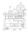
- FIGS. 3-5present cross-section views of an exemplary apparatus 300 at various stages of a method that includes reversibly controlling a contact angle of a fluid disposed on a substrate surface.
- the viewsare analogous to the view presented in FIG. 2 , but at a lower magnification. Any of the various embodiments of the present inventions discussed above and illustrated in FIG. 1-2 could be used in the method.
- FIGS. 3-5use the same reference numbers to depict analogous structures shown in FIGS. 1-2 .
- each of the closed-cells 105comprise one or more internal walls 115 that divide an interior of each of the closed-cells 105 into a first zone 120 and a plurality of second zones 125 .
- the first zone 120occupies a larger area of each of the closed-cells 105 than any one second zone 125 and the first and second zones 120 , 125 are interconnected to form a common volume.
- the apparatus 300it is desirable to reversibly adjust the degree of wetting of the surface 110 that the fluid 220 is disposed on. For example it is advantageous to suspend the fluid 220 on a surface 110 that is de-wetted, so that the fluid 220 can be easily moved over the surface 110 .
- the surface 110is considered de-wetted if a droplet of fluid 220 on the surface 110 forms a contact angle 235 of 140 degrees or greater. In some cases the contact angle 235 of a de-wetted surface 110 is greater than or equal to about 170 degrees.
- the degree of wetting of the surface 110can be reversibly controlled by adjusting a pressure of a medium 215 located inside one or more of the closed-cells 105 , thereby changing the contact angle 235 of the fluid 220 with the substrate surface 110 .
- An increase in pressure due to heating the medium 215can cause the contact angle 235 to increase.
- a decrease in pressure due to cooling the medium 215can cause the contact angle 235 to decrease.
- the contact angle 235can be reversibly changed.
- the contact angle 235can be increased and then decreased, or vice-versa, by at least about 1° per 1 degree Celsius change in a temperature of the medium 215 .
- the contact angle 235can be reversibly changed by at least about 50° for an about 50 degree Celsius change in a temperature of the medium 215 .
- the surface 110can be de-wetted by increasing the pressure of the medium 215 , thereby causing the medium 215 to exert an increased force against the fluid 220 .
- the pressure of the medium 215can be increased by increasing the medium's temperature, for example, by heating the closed-cells 105 that holds the medium 215 .
- the cells 105are heated indirectly by heating the substrate 150 via a temperature-regulating device 230 that is thermally coupled to the substrate 150 .
- the cells 105are heated directly by passing a current through the cells 105 via an electrical source 240 that is electrically coupled to the cells 105 .
- FIG. 4illustrated is the apparatus 300 after moving the droplet of the fluid 220 to a desired location 400 , and then wetting the surface so that the fluid 220 becomes immobilized at the desired location 400 .
- Those skilled in the artwould be familiar any number of methods that could be used to move the fluid 220 .
- U.S. Patent Application No. 2004/0191127which is incorporated herein in its totality, discusses methods to control the movement of a liquid on a microstructured or nanostructured surface.
- wettingis considered to have occurred if a droplet of fluid 220 on the surface 110 forms a contact angle 235 of 90 degrees or less. In some cases, the contact angle 235 of a wetted surface 110 is less than or equal to about 70 degrees.
- the surface 110can be wetted by decreasing the pressure of the medium 215 , thereby causing the medium 215 to exert less force against the fluid 220 .
- the pressure of the medium 215can be reduced by decreasing the medium's temperature, for example, by cooling the cells 105 that hold the medium 215 .
- the cells 105can be cooled indirectly by cooling the substrate 150 via the temperature-regulating device 230 .
- the cells 105can be cooled directly by turning off or decreasing a current passed through the cells via the electrical source 240 .
- wettingis accomplished by applying a voltage between the cells 105 and the fluid 220 via the electrical source 240 , or another electrical source 250 , to electro-wet the surface 110 .
- wettingcauses the fluid 220 to be drawn into at least one of the closed-cells 105 .
- the fluid 220penetrates into the first zone 120 of the closed-cell 105 to a greater extent than the plurality of second zones 125 of the cell 105 .
- the fluid 220contacts an analytical depot 410 located on or in the substrate 150 .
- the analytical depot 410can comprise any conventional structures or materials to facilitate the identification or characterization of some property of the fluid 220 .
- the analytical depot 410can comprise a reagent configured to interact with the fluid 410 thereby identifying a property of the fluid 220 .
- the analytical depot 410can comprise an field-effect transistor configured to generate an electrical signal when it comes in contact with a particular type of fluid 220 or a compound dissolved or suspended in the fluid 220 .
- the apparatus 300after de-wetting the surface 110 so that the fluid 220 is re-mobilized to facilitate the fluid's movement to another location 500 on the surface 110 .
- Any of the above-described methodscan be performed to repeatedly wet and de-wet the fluid 220 .
- the above-described methodscan be used in combination to increase the extent of wetting or de-wetting, if desired.
- the cells 105 that the fluid 220 is located oncan be de-wetted through a combination of direct heating, by applying the current, indirect heating, via the temperature-regulating device 230 , and turning off the voltage.
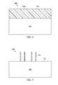
- FIGS. 6-9present cross-section views of an exemplary apparatus 600 at selected stages of manufacture.
- the cross-sectional view of the exemplary apparatus 600corresponds to view line 2 - 2 in FIG. 1 .
- the same reference numbersare used to depict analogous structures shown in FIGS. 1-5 . Any of the above-described embodiments of apparatuses can be manufactured by the method.
- FIG. 6shown is the partially-completed apparatus 600 after providing a substrate 150 and depositing a photoresist layer 610 on a surface 110 of the substrate 150 .
- Preferred embodiments of the substrate 150can comprise silicon or silicon-on-insulator (SOI). Any conventional photoresist material designed for use in dry-etch applications may be used to form the photoresist layer 610 .
- FIG. 7illustrates the partially-completed apparatus 600 after defining a photoresist pattern 710 in the photoresist layer 610 ( FIG. 6 ) and removing those portions of the layer 610 that lay outside the pattern.
- the photoresist pattern 710comprises the layout of internal and external walls for the closed-cells of the apparatus 600 .
- FIG. 8presents the partially-completed apparatus 600 after forming a plurality of closed-cells 105 on the surface 110 of the substrate 150 and removing the photoresist pattern 710 ( FIG. 7 ).
- each of the closed-cells 105comprise one or more internal walls 115 that divide an interior of each of the closed-cells 105 into a single first zone 120 and a plurality of second zones 125 .
- the first zone 120occupies a larger area of the closed-cell 105 than any one of the second zones 125 and the first and second zones 120 , 125 are interconnected to form a common volume.
- the closed-cells 105are formed by removing portions of the substrate 150 that are not under the photoresist pattern 710 depicted in FIG. 7 to depths 210 up to about 50 microns.
- the remaining portions of the substrate 150comprise internal walls 115 and external walls 140 of the cells 105 .
- portions of the substrate 150are removed using conventional dry-etching procedures, for example, deep reactive ion etching, or other procedures well-known to those skilled in the art.
- FIG. 9illustrates the partially-completed apparatus 600 after coupling a temperature-regulating device 230 to the substrate 150 .
- the temperature regulating device 230is coupled to a surface 900 of the substrate 150 that is on the opposite side of the surface 110 that the closed-cells 105 are formed on.
- surface 110 , internal walls 115 and external walls 140 of the cells 105are covered with an insulating layer 910 .
- the insulating layer 910facilitates the electrowetting of the surface 110 , as further discussed in the is discussed in U.S. Pat. No. 6,538,823.
- an insulating layer 910 of silicon oxide dielectricis added to the apparatus 600 by thermal oxidation.
- FIG. 9also illustrates the partially-completed apparatus 600 after forming an analytical depot 410 located in the first zone 120 .
- the analytical depot 410is configured to interact with a sample deposited on the apparatus 600 , thereby identifying a property of fluid 200 deposited on the apparatus 600 , such as discussed above in the context of FIGS. 3-5 .
- forming the analytical depot 410can comprise depositing a reagent into the first zone 120 .
- the reagentcan be placed over the first zone and then the cell 105 is electrowetted so that the reagent enters the first zone 120 .
- the regentcan be delivered directly into the first zone 120 using a micro-volume delivery device, such as a micro-pipette.
- the analytical depot 410can be formed by fabricating a field-effect transistor (FET) using conventional process well-known to those in the semiconductor industry.
- FETfield-effect transistor
- the FETis located in the first zone 120 .
- the FETcan be configured to generate an electrical signal when it comes in contact with a particular type of fluid 200 or material of interest dissolved or suspended in the fluid 200 .
Landscapes
- Chemical & Material Sciences (AREA)
- Dispersion Chemistry (AREA)
- Health & Medical Sciences (AREA)
- Analytical Chemistry (AREA)
- General Health & Medical Sciences (AREA)
- Hematology (AREA)
- Clinical Laboratory Science (AREA)
- Chemical Kinetics & Catalysis (AREA)
- Apparatus Associated With Microorganisms And Enzymes (AREA)
Abstract
Description
Claims (19)
Priority Applications (1)
| Application Number | Priority Date | Filing Date | Title |
|---|---|---|---|
| US11/227,663US8287808B2 (en) | 2005-09-15 | 2005-09-15 | Surface for reversible wetting-dewetting |
Applications Claiming Priority (1)
| Application Number | Priority Date | Filing Date | Title |
|---|---|---|---|
| US11/227,663US8287808B2 (en) | 2005-09-15 | 2005-09-15 | Surface for reversible wetting-dewetting |
Publications (2)
| Publication Number | Publication Date |
|---|---|
| US20070059510A1 US20070059510A1 (en) | 2007-03-15 |
| US8287808B2true US8287808B2 (en) | 2012-10-16 |
Family
ID=37855530
Family Applications (1)
| Application Number | Title | Priority Date | Filing Date |
|---|---|---|---|
| US11/227,663Expired - Fee RelatedUS8287808B2 (en) | 2005-09-15 | 2005-09-15 | Surface for reversible wetting-dewetting |
Country Status (1)
| Country | Link |
|---|---|
| US (1) | US8287808B2 (en) |
Cited By (10)
| Publication number | Priority date | Publication date | Assignee | Title |
|---|---|---|---|---|
| US9314818B2 (en) | 2010-07-27 | 2016-04-19 | The Regents Of The University Of California | Method and device for restoring and maintaining superhydrophobicity under liquid |
| WO2016161402A1 (en) | 2015-04-03 | 2016-10-06 | Abbott Laboratories | Devices and methods for sample analysis |
| WO2017004463A1 (en) | 2015-07-01 | 2017-01-05 | Abbott Laboratories | Devices and methods for sample analysis |
| WO2018067878A1 (en) | 2016-10-05 | 2018-04-12 | Abbott Laboratories | Devices and methods for sample analysis |
| WO2019213583A1 (en) | 2018-05-04 | 2019-11-07 | Abbott Laboratories | Sequential sampling method for improving immunoassay sensitivity and kinetics of small volume samples |
| WO2020140071A1 (en) | 2018-12-28 | 2020-07-02 | Abbott Laboratories | Direct detection of single molecules on microparticles |
| WO2021026402A1 (en) | 2019-08-07 | 2021-02-11 | Abbott Laboratories | Chemiluminescent compounds for multiplexing |
| WO2021026403A1 (en) | 2019-08-07 | 2021-02-11 | Abbott Laboratories | Methods for detecting assay interferents and increasing dynamic range |
| US11633738B2 (en) | 2015-04-03 | 2023-04-25 | Abbott Laboratories | Devices and methods for sample analysis |
| US12365585B2 (en) | 2014-07-18 | 2025-07-22 | The Regents Of The University Of California | Method of forming a microstructured surface |
Families Citing this family (4)
| Publication number | Priority date | Publication date | Assignee | Title |
|---|---|---|---|---|
| US7449649B2 (en)* | 2006-05-23 | 2008-11-11 | Lucent Technologies Inc. | Liquid switch |
| EP2188669B1 (en)* | 2007-09-12 | 2017-01-11 | University Of Cincinnati | Electrofluidic devices, visual displays, and methods for making and operating such electrofluidic devices |
| US20100112286A1 (en)* | 2008-11-03 | 2010-05-06 | Bahadur Vaibhav A | Superhydrophobic surfaces |
| WO2014175980A2 (en)* | 2013-03-20 | 2014-10-30 | Massachusetts Institute Of Technology | Condensation on surfaces |
Citations (67)
| Publication number | Priority date | Publication date | Assignee | Title |
|---|---|---|---|---|
| US3454686A (en) | 1964-10-29 | 1969-07-08 | Harry S Jones | Method of shaping an aspheric lens |
| US3670130A (en) | 1969-03-07 | 1972-06-13 | Int Standard Electric Corp | Improvements in electrostatic relays |
| US4030813A (en) | 1974-12-20 | 1977-06-21 | Matsushita Electric Industrial Co., Ltd. | Control element having liquid layer attainable to geometrically uneven state in response to electrical signal |
| US4118270A (en) | 1976-02-18 | 1978-10-03 | Harris Corporation | Micro lens formation at optical fiber ends |
| US4137060A (en) | 1977-07-18 | 1979-01-30 | Robert Bosch Gmbh | Method of forming a lens at the end of a light guide |
| US4338352A (en) | 1981-02-23 | 1982-07-06 | Mcdonnell Douglas Corporation | Process for producing guided wave lens on optical fibers |
| US4406732A (en) | 1981-03-17 | 1983-09-27 | Thomson-Csf | Process for the controlled modification of the geometrical-characteristics of the end of a monomode optical fiber and application thereof to optical coupling |
| US4569575A (en) | 1983-06-30 | 1986-02-11 | Thomson-Csf | Electrodes for a device operating by electrically controlled fluid displacement |
| US4653847A (en) | 1981-02-23 | 1987-03-31 | Motorola, Inc. | Fiber optics semiconductor package |
| US4671609A (en) | 1982-12-23 | 1987-06-09 | U.S. Philips Corporation | Coupling monomode optical fiber having a tapered end portion |
| US4708426A (en) | 1984-07-09 | 1987-11-24 | U.S. Philips Corp. | Electro-optical device comprising a laser diode, and input transmission fibre and an output transmission fibre |
| US4783155A (en) | 1983-10-17 | 1988-11-08 | Canon Kabushiki Kaisha | Optical device with variably shaped optical surface and a method for varying the focal length |
| EP0290125A2 (en) | 1987-05-05 | 1988-11-09 | Molecular Devices Corporation | Hydrophilic microplates for vertical beam photometry |
| US4784479A (en) | 1984-05-30 | 1988-11-15 | Canon Kabushiki Kaisha | Varifocal optical system |
| US4867521A (en) | 1984-08-20 | 1989-09-19 | British Telecommunications Public Limited Company | Microlens manufacture |
| US4948214A (en) | 1989-07-10 | 1990-08-14 | Eastman Kodak Company | Step-index light guide and gradient index microlens device for LED imaging |
| US5248734A (en) | 1992-06-16 | 1993-09-28 | Cornell Research Foundation, Inc. | Process for preparing a polyphenylene polymer |
| US5348687A (en) | 1993-11-26 | 1994-09-20 | Mobil Oil Corp. | M41S materials having nonlinear optical properties |
| US5412746A (en) | 1993-03-30 | 1995-05-02 | Alcatel N.V. | Optical coupler and amplifier |
| US5428711A (en) | 1991-01-09 | 1995-06-27 | Matsushita Electric Industrial Co., Ltd. | Spatial light modulator and neural network |
| US5486337A (en) | 1994-02-18 | 1996-01-23 | General Atomics | Device for electrostatic manipulation of droplets |
| US5518863A (en) | 1992-01-31 | 1996-05-21 | Institut National D'optique | Method of changing the optical invariant of multifiber fiber-optic elements |
| US5659330A (en) | 1996-05-31 | 1997-08-19 | Xerox Corporation | Electrocapillary color display sheet |
| US5665527A (en) | 1995-02-17 | 1997-09-09 | International Business Machines Corporation | Process for generating negative tone resist images utilizing carbon dioxide critical fluid |
| DE19623270A1 (en) | 1996-06-11 | 1998-01-15 | Juergen Rebel | Adaptive optical laser imaging apparatus for information recording |
| DE19704207A1 (en) | 1997-02-05 | 1998-08-13 | Hermann Josef Wilhelm | Low drag hull |
| FR2769375A1 (en) | 1997-10-08 | 1999-04-09 | Univ Joseph Fourier | Variable focus optical lens comprising liquid droplet |
| US5922299A (en) | 1996-11-26 | 1999-07-13 | Battelle Memorial Institute | Mesoporous-silica films, fibers, and powders by evaporation |
| US5948470A (en) | 1997-04-28 | 1999-09-07 | Harrison; Christopher | Method of nanoscale patterning and products made thereby |
| WO1999054730A1 (en) | 1998-04-20 | 1999-10-28 | Wallac Oy | Method and device for carrying out a chemical analysis in small amounts of liquid |
| US6014259A (en) | 1995-06-07 | 2000-01-11 | Wohlstadter; Jacob N. | Three dimensional imaging system |
| US6027666A (en) | 1998-06-05 | 2000-02-22 | The Governing Council Of The University Of Toronto | Fast luminescent silicon |
| US6156283A (en)* | 1998-03-23 | 2000-12-05 | Engelhard Corporation | Hydrophobic catalytic materials and method of forming the same |
| US6185961B1 (en) | 1999-01-27 | 2001-02-13 | The United States Of America As Represented By The Secretary Of The Navy | Nanopost arrays and process for making same |
| WO2001031404A1 (en) | 1999-10-26 | 2001-05-03 | Cornell Research Foundation, Inc. | Using block copolymers as supercritical fluid developable photoresists |
| WO2001042540A1 (en) | 1999-12-09 | 2001-06-14 | Cornell Research Foundation, Inc. | Fabrication of periodic surface structures with nanometer-scale spacings |
| WO2001051990A1 (en) | 2000-01-12 | 2001-07-19 | Semiconductor Research Corp. | Solventless, resistless direct dielectric patterning |
| EP1120164A2 (en) | 2000-01-28 | 2001-08-01 | Roche Diagnostics GmbH | Fluid flow control in curved capillary channels |
| US6387453B1 (en) | 2000-03-02 | 2002-05-14 | Sandia Corporation | Method for making surfactant-templated thin films |
| US6409907B1 (en) | 1999-02-11 | 2002-06-25 | Lucent Technologies Inc. | Electrochemical process for fabricating article exhibiting substantial three-dimensional order and resultant article |
| US6431695B1 (en)* | 1998-06-18 | 2002-08-13 | 3M Innovative Properties Company | Microstructure liquid dispenser |
| US20020125192A1 (en) | 2001-02-14 | 2002-09-12 | Lopez Gabriel P. | Nanostructured devices for separation and analysis |
| US6465387B1 (en) | 1999-08-12 | 2002-10-15 | Board Of Trustees Of Michigan State University | Combined porous organic and inorganic oxide materials prepared by non-ionic surfactant templating route |
| US6471761B2 (en) | 2000-04-21 | 2002-10-29 | University Of New Mexico | Prototyping of patterned functional nanostructures |
| US6473543B2 (en) | 1998-03-09 | 2002-10-29 | Bartels Mikrotechnik Gmbh | Optical component |
| US20030020915A1 (en) | 1998-03-23 | 2003-01-30 | Schueller Olivier J. A. | Optical modulator/detector based on reconfigurable diffraction grating |
| US6538823B2 (en) | 2001-06-19 | 2003-03-25 | Lucent Technologies Inc. | Tunable liquid microlens |
| US6545815B2 (en) | 2001-09-13 | 2003-04-08 | Lucent Technologies Inc. | Tunable liquid microlens with lubrication assisted electrowetting |
| US6545816B1 (en) | 2001-10-19 | 2003-04-08 | Lucent Technologies Inc. | Photo-tunable liquid microlens |
| WO2003056330A2 (en) | 2001-12-31 | 2003-07-10 | Institut für Physikalische Hochtechnologie e.V. | Cell sorting system for the size-based sorting or separation of cells suspended in a flowing fluid |
| US20030148401A1 (en) | 2001-11-09 | 2003-08-07 | Anoop Agrawal | High surface area substrates for microarrays and methods to make same |
| WO2003071335A2 (en) | 2002-02-20 | 2003-08-28 | Koninklijke Philips Electronics N.V. | Display apparatus |
| WO2003083447A1 (en) | 2002-03-22 | 2003-10-09 | Diversa Corporation | A method for intensifying the optical detection of samples that are held in solution in the through-hole wells of a holding tray |
| WO2003103835A1 (en) | 2002-06-07 | 2003-12-18 | Åmic AB | Micro fluidic structures |
| US20040058450A1 (en) | 2002-09-24 | 2004-03-25 | Pamula Vamsee K. | Methods and apparatus for manipulating droplets by electrowetting-based techniques |
| US20040191127A1 (en) | 2003-03-31 | 2004-09-30 | Avinoam Kornblit | Method and apparatus for controlling the movement of a liquid on a nanostructured or microstructured surface |
| US20050039661A1 (en) | 2003-08-22 | 2005-02-24 | Avinoam Kornblit | Method and apparatus for controlling friction between a fluid and a body |
| US20050069458A1 (en) | 2003-09-30 | 2005-03-31 | Hodes Marc Scott | Method and apparatus for controlling the flow resistance of a fluid on nanostructured or microstructured surfaces |
| US6891682B2 (en) | 2003-03-03 | 2005-05-10 | Lucent Technologies Inc. | Lenses with tunable liquid optical elements |
| US20060172189A1 (en) | 2005-01-31 | 2006-08-03 | Kolodner Paul R | Graphitic nanostructured battery |
| US20070048858A1 (en) | 2005-08-31 | 2007-03-01 | Lucent Technologies Inc. | Low adsorption surface |
| US20070056853A1 (en) | 2005-09-15 | 2007-03-15 | Lucnet Technologies Inc. | Micro-chemical mixing |
| US20070059213A1 (en) | 2005-09-15 | 2007-03-15 | Lucent Technologies Inc. | Heat-induced transitions on a structured surface |
| US20070059489A1 (en) | 2005-09-15 | 2007-03-15 | Lucent Technologies Inc. | Structured surfaces with controlled flow resistance |
| US7204298B2 (en) | 2004-11-24 | 2007-04-17 | Lucent Technologies Inc. | Techniques for microchannel cooling |
| US20070237025A1 (en) | 2006-03-28 | 2007-10-11 | Lucent Technologies Inc. | Multilevel structured surfaces |
| US20070272528A1 (en) | 2006-05-23 | 2007-11-29 | Lucent Technologies Inc. | Liquid switch |
Family Cites Families (1)
| Publication number | Priority date | Publication date | Assignee | Title |
|---|---|---|---|---|
| US6228116B1 (en)* | 1987-12-22 | 2001-05-08 | Walter J. Ledergerber | Tissue expander |
- 2005
- 2005-09-15USUS11/227,663patent/US8287808B2/ennot_activeExpired - Fee Related
Patent Citations (73)
| Publication number | Priority date | Publication date | Assignee | Title |
|---|---|---|---|---|
| US3454686A (en) | 1964-10-29 | 1969-07-08 | Harry S Jones | Method of shaping an aspheric lens |
| US3670130A (en) | 1969-03-07 | 1972-06-13 | Int Standard Electric Corp | Improvements in electrostatic relays |
| US4030813A (en) | 1974-12-20 | 1977-06-21 | Matsushita Electric Industrial Co., Ltd. | Control element having liquid layer attainable to geometrically uneven state in response to electrical signal |
| US4118270A (en) | 1976-02-18 | 1978-10-03 | Harris Corporation | Micro lens formation at optical fiber ends |
| US4137060A (en) | 1977-07-18 | 1979-01-30 | Robert Bosch Gmbh | Method of forming a lens at the end of a light guide |
| US4653847A (en) | 1981-02-23 | 1987-03-31 | Motorola, Inc. | Fiber optics semiconductor package |
| US4338352A (en) | 1981-02-23 | 1982-07-06 | Mcdonnell Douglas Corporation | Process for producing guided wave lens on optical fibers |
| US4406732A (en) | 1981-03-17 | 1983-09-27 | Thomson-Csf | Process for the controlled modification of the geometrical-characteristics of the end of a monomode optical fiber and application thereof to optical coupling |
| US4671609A (en) | 1982-12-23 | 1987-06-09 | U.S. Philips Corporation | Coupling monomode optical fiber having a tapered end portion |
| US4569575A (en) | 1983-06-30 | 1986-02-11 | Thomson-Csf | Electrodes for a device operating by electrically controlled fluid displacement |
| US4783155A (en) | 1983-10-17 | 1988-11-08 | Canon Kabushiki Kaisha | Optical device with variably shaped optical surface and a method for varying the focal length |
| US4784479A (en) | 1984-05-30 | 1988-11-15 | Canon Kabushiki Kaisha | Varifocal optical system |
| US4708426A (en) | 1984-07-09 | 1987-11-24 | U.S. Philips Corp. | Electro-optical device comprising a laser diode, and input transmission fibre and an output transmission fibre |
| US4867521A (en) | 1984-08-20 | 1989-09-19 | British Telecommunications Public Limited Company | Microlens manufacture |
| EP0290125A2 (en) | 1987-05-05 | 1988-11-09 | Molecular Devices Corporation | Hydrophilic microplates for vertical beam photometry |
| US4948214A (en) | 1989-07-10 | 1990-08-14 | Eastman Kodak Company | Step-index light guide and gradient index microlens device for LED imaging |
| US5428711A (en) | 1991-01-09 | 1995-06-27 | Matsushita Electric Industrial Co., Ltd. | Spatial light modulator and neural network |
| US5518863A (en) | 1992-01-31 | 1996-05-21 | Institut National D'optique | Method of changing the optical invariant of multifiber fiber-optic elements |
| US5248734A (en) | 1992-06-16 | 1993-09-28 | Cornell Research Foundation, Inc. | Process for preparing a polyphenylene polymer |
| US5412746A (en) | 1993-03-30 | 1995-05-02 | Alcatel N.V. | Optical coupler and amplifier |
| US5348687A (en) | 1993-11-26 | 1994-09-20 | Mobil Oil Corp. | M41S materials having nonlinear optical properties |
| US5486337A (en) | 1994-02-18 | 1996-01-23 | General Atomics | Device for electrostatic manipulation of droplets |
| US5665527A (en) | 1995-02-17 | 1997-09-09 | International Business Machines Corporation | Process for generating negative tone resist images utilizing carbon dioxide critical fluid |
| US6014259A (en) | 1995-06-07 | 2000-01-11 | Wohlstadter; Jacob N. | Three dimensional imaging system |
| US5659330A (en) | 1996-05-31 | 1997-08-19 | Xerox Corporation | Electrocapillary color display sheet |
| DE19623270A1 (en) | 1996-06-11 | 1998-01-15 | Juergen Rebel | Adaptive optical laser imaging apparatus for information recording |
| US5922299A (en) | 1996-11-26 | 1999-07-13 | Battelle Memorial Institute | Mesoporous-silica films, fibers, and powders by evaporation |
| DE19704207A1 (en) | 1997-02-05 | 1998-08-13 | Hermann Josef Wilhelm | Low drag hull |
| US5948470A (en) | 1997-04-28 | 1999-09-07 | Harrison; Christopher | Method of nanoscale patterning and products made thereby |
| FR2769375A1 (en) | 1997-10-08 | 1999-04-09 | Univ Joseph Fourier | Variable focus optical lens comprising liquid droplet |
| WO1999018456A1 (en) | 1997-10-08 | 1999-04-15 | Universite Joseph Fourier | Lens with variable focus |
| US6369954B1 (en) | 1997-10-08 | 2002-04-09 | Universite Joseph Fourier | Lens with variable focus |
| US6473543B2 (en) | 1998-03-09 | 2002-10-29 | Bartels Mikrotechnik Gmbh | Optical component |
| US6156283A (en)* | 1998-03-23 | 2000-12-05 | Engelhard Corporation | Hydrophobic catalytic materials and method of forming the same |
| US20030020915A1 (en) | 1998-03-23 | 2003-01-30 | Schueller Olivier J. A. | Optical modulator/detector based on reconfigurable diffraction grating |
| WO1999054730A1 (en) | 1998-04-20 | 1999-10-28 | Wallac Oy | Method and device for carrying out a chemical analysis in small amounts of liquid |
| US6027666A (en) | 1998-06-05 | 2000-02-22 | The Governing Council Of The University Of Toronto | Fast luminescent silicon |
| US6319427B1 (en) | 1998-06-05 | 2001-11-20 | Geoffrey A. Ozin | Fast luminescent silicon |
| US6431695B1 (en)* | 1998-06-18 | 2002-08-13 | 3M Innovative Properties Company | Microstructure liquid dispenser |
| US6185961B1 (en) | 1999-01-27 | 2001-02-13 | The United States Of America As Represented By The Secretary Of The Navy | Nanopost arrays and process for making same |
| US6409907B1 (en) | 1999-02-11 | 2002-06-25 | Lucent Technologies Inc. | Electrochemical process for fabricating article exhibiting substantial three-dimensional order and resultant article |
| US6465387B1 (en) | 1999-08-12 | 2002-10-15 | Board Of Trustees Of Michigan State University | Combined porous organic and inorganic oxide materials prepared by non-ionic surfactant templating route |
| WO2001031404A1 (en) | 1999-10-26 | 2001-05-03 | Cornell Research Foundation, Inc. | Using block copolymers as supercritical fluid developable photoresists |
| US6379874B1 (en) | 1999-10-26 | 2002-04-30 | Cornell Research Foundation, Inc. | Using block copolymers as supercritical fluid developable photoresists |
| WO2001042540A1 (en) | 1999-12-09 | 2001-06-14 | Cornell Research Foundation, Inc. | Fabrication of periodic surface structures with nanometer-scale spacings |
| US6329070B1 (en) | 1999-12-09 | 2001-12-11 | Cornell Research Foundation, Inc. | Fabrication of periodic surface structures with nanometer-scale spacings |
| WO2001051990A1 (en) | 2000-01-12 | 2001-07-19 | Semiconductor Research Corp. | Solventless, resistless direct dielectric patterning |
| EP1120164A2 (en) | 2000-01-28 | 2001-08-01 | Roche Diagnostics GmbH | Fluid flow control in curved capillary channels |
| US6387453B1 (en) | 2000-03-02 | 2002-05-14 | Sandia Corporation | Method for making surfactant-templated thin films |
| US6471761B2 (en) | 2000-04-21 | 2002-10-29 | University Of New Mexico | Prototyping of patterned functional nanostructures |
| US20020125192A1 (en) | 2001-02-14 | 2002-09-12 | Lopez Gabriel P. | Nanostructured devices for separation and analysis |
| US6538823B2 (en) | 2001-06-19 | 2003-03-25 | Lucent Technologies Inc. | Tunable liquid microlens |
| US6545815B2 (en) | 2001-09-13 | 2003-04-08 | Lucent Technologies Inc. | Tunable liquid microlens with lubrication assisted electrowetting |
| US6545816B1 (en) | 2001-10-19 | 2003-04-08 | Lucent Technologies Inc. | Photo-tunable liquid microlens |
| US20030148401A1 (en) | 2001-11-09 | 2003-08-07 | Anoop Agrawal | High surface area substrates for microarrays and methods to make same |
| WO2003056330A2 (en) | 2001-12-31 | 2003-07-10 | Institut für Physikalische Hochtechnologie e.V. | Cell sorting system for the size-based sorting or separation of cells suspended in a flowing fluid |
| WO2003071335A2 (en) | 2002-02-20 | 2003-08-28 | Koninklijke Philips Electronics N.V. | Display apparatus |
| WO2003083447A1 (en) | 2002-03-22 | 2003-10-09 | Diversa Corporation | A method for intensifying the optical detection of samples that are held in solution in the through-hole wells of a holding tray |
| WO2003103835A1 (en) | 2002-06-07 | 2003-12-18 | Åmic AB | Micro fluidic structures |
| US20050042766A1 (en)* | 2002-06-07 | 2005-02-24 | Amic Ab | Micro fluidic structures |
| US20040058450A1 (en) | 2002-09-24 | 2004-03-25 | Pamula Vamsee K. | Methods and apparatus for manipulating droplets by electrowetting-based techniques |
| US6891682B2 (en) | 2003-03-03 | 2005-05-10 | Lucent Technologies Inc. | Lenses with tunable liquid optical elements |
| US20040191127A1 (en) | 2003-03-31 | 2004-09-30 | Avinoam Kornblit | Method and apparatus for controlling the movement of a liquid on a nanostructured or microstructured surface |
| US20050039661A1 (en) | 2003-08-22 | 2005-02-24 | Avinoam Kornblit | Method and apparatus for controlling friction between a fluid and a body |
| US20050069458A1 (en) | 2003-09-30 | 2005-03-31 | Hodes Marc Scott | Method and apparatus for controlling the flow resistance of a fluid on nanostructured or microstructured surfaces |
| US7204298B2 (en) | 2004-11-24 | 2007-04-17 | Lucent Technologies Inc. | Techniques for microchannel cooling |
| US20060172189A1 (en) | 2005-01-31 | 2006-08-03 | Kolodner Paul R | Graphitic nanostructured battery |
| US20070048858A1 (en) | 2005-08-31 | 2007-03-01 | Lucent Technologies Inc. | Low adsorption surface |
| US20070056853A1 (en) | 2005-09-15 | 2007-03-15 | Lucnet Technologies Inc. | Micro-chemical mixing |
| US20070059213A1 (en) | 2005-09-15 | 2007-03-15 | Lucent Technologies Inc. | Heat-induced transitions on a structured surface |
| US20070059489A1 (en) | 2005-09-15 | 2007-03-15 | Lucent Technologies Inc. | Structured surfaces with controlled flow resistance |
| US20070237025A1 (en) | 2006-03-28 | 2007-10-11 | Lucent Technologies Inc. | Multilevel structured surfaces |
| US20070272528A1 (en) | 2006-05-23 | 2007-11-29 | Lucent Technologies Inc. | Liquid switch |
Non-Patent Citations (87)
| Title |
|---|
| "Sol-Gel Chemistry," published online at http://www.sol-gel.com/chemi.htm, Dec. 9, 2002, 2 pages. |
| Abbot, N.L., et al. "Potential-Dependent Wetting of Aqubous Solutions on Self-Assembled Monolayers Formed from 15-(Ferrocenylcarbonyl) Pentadecaneithiol on Gold," Langmuir 1994, American Chemical Society, vol. 10, pp. 1493-1497. |
| Abbot, N.L., et al., "Potential-Dependent Wetting of Aqueous Solutions on Self-Assembled Monolayers Formed from 15-(Ferrocenylcarbonyl) pentadecanethiol on Gold," Langmuir 1994, American Chemical Society vol. 10, pp. 1493-1497. |
| Aizenberg, J., et al., "Calcitic microlenses as part of the photoreceptor system in brittlestars," Nature, vol. 412, pp. 819-822, Aug. 23, 2001. |
| Arsenault, A.C., et al., "A Polychromic, Fast Response Metallopolymer Gel Photonic Crystal with Solvant and Redox Tunability: A Step Towards Photonic Ink (P-Ink)," Adv. Mater. 2003, 15, No. 6, Mar. 17, 2003, pp. 503-507. |
| Avgeropoulos, et al., "Synthesis and Morphological Behavior of Silicon-Containing Triblock Copolymers for Nanostructure Applications," Chem. Mater. 1998, 10, pp. 2109-2115. |
| Baney, et al., "Silsesquioxanes," American Chemical Society, 1995, pp. 1409-1430. |
| Bell Labs scientists discover technique to control fluids using specially fabricated silicon "nanograss"; Lucent Technologies, press release Mar. 12, 2004. 3 Pages (no longer available on Lucent's press archive, but available through the Internet Archive). |
| Bhardwaj, et al., "Advances in High Rate Silicon and Oxide Etching using ICP", STS Ltd., Imperial Park, Newport, UK NP10 89UJ (6 pags). |
| Brinker, C.J., et al., "Evaporation-Induced Self-Assembly: Nanostructures Made Easy**" Advanced Materials. vol. 11. 1999. pp. 579-585. |
| Campbell, D.J., et al., "Replication and Compression of Bulk and Surface Structures with Pholydimethylsiloxane Elastomer," Journal of Chemical Education, vol. 75, No. 4, Apr. 1999, pp. 537-541. |
| Campbell, M., et al., "Fabrication of Photonic Crystals for The Visible Spectrum by Holographic Lithography," Nature, vol. 404, Mar. 2, 2000, pp. 53-56. |
| Chan, Vanessa A-H., et al., "Ordered Bicontinuous Nanoporous and Nanorelief Ceramic Films from Self-Assembling Polymer Precursors," Science, Nov. 26, 1999, vol. 286, pp. 1716-1719. |
| Chang, Kenneth, 'Nanograss' Turns Sticky to Slippery in an Instant, The New York Times, Mar. 16, 2004, 2 Pages. |
| Commander, L.G. et al., "Variable Focal Length Microlenses," Optics Communications 177. Apr. 15, 2000. pp. 157-170. |
| Danzerbrink, R. et al., "Deposition of Micropatterned Coating Using an Ink-Jet Technique," Thin Solid Films 351, pp. 115-118, Elsevier Science S.A. (1999). |
| E.W. Becker, et al., "Fabrication of microstructures with high aspect ratios and great structural heights by synchrotron radiation lithography, galvanoforming, and plastic moulding (LIGA process)", Microelectronic Engineering Elsevier Publishers BV, Amsterdam, NI, vol. 4, No. 1 (May 1, 1986), pp. 35-56. |
| eFunda: General Information on Element Silicon, accessed at http://www.efunda.com/materials/elements/element-info.cfm?Element-ID=Si, Aug. 10, 2005 (8 pages). |
| English language translation of abstract for German Patent Document: DE 19623270 from European Patent Office database, esp@cenet.com, (1998), 1 page. |
| Feng, Chuan Liang et al., "Reversible Wettability of Photoresponsive Flourine-Containing Azobenzene Polymer in Langmuir-Blodgett Films," Lengmuir vol. 17, No. 15, 2001, pp. 4593-4597, American Chemical Society published on Web Jun. 22, 2001. |
| Glod, et al., "An investigation of microscale explosive vaporization of water on an utrathin Pt wire", International Journal of Heat and Mass Transfer 45 (2002), pp. 367-379. |
| Gonsalves, Antone, Bell Labs Invention Could Mean Cooler Chips, Techweb Network, Mar. 12, 2004, 2 Pages. |
| Ho, K.M., et al., "Existence of a Photonic Gap in Periodic Dielectric Structures," Physical Review Letters, vol. 65, No. 25, Dec. 17, 1990, pp. 3152-3155. |
| Huo, Q. et al: "Generalized synthesis of periodic surfactant/inorganic composite materials," NATURE, vol. 368. Mar. 1994, pp. 317-321. |
| Ichimura, Kunihiro et al., "Light-Driven Motion of Liquids on a Photoresponsive Surface." Science. vol. 288. Jun. 2, 2000. pp. 1624-1626. |
| Jahns, J., et al., "Microoptics for biomedical applications," American Biotechnology Laboratory, No. 18. Oct. 2000, pp. 52 and 54. |
| Kim, et al, "Nanostructured Surfaces for Dramatic Reduction of Flow Resistance in Drop[let-Based Microfluidics." IEEE, pp. 479-482 (2002). |
| Kresge, C.T., et al: "Ordered mesoporous molecular sievas synthesized by a liquid-crystal template mechanism" Nature, vol. 359, Oct. 1992, pp. 710-712. |
| Kruk, M., et al., "Mesoporous Silicate-Surfactant Composites with Hydrophobic Surfaces and Tailored Pore Sizes"; Journal of Physical Chemistry 106 B (2002) pp. 10096-10101. |
| Krupenkin, et al.; From rolling ball to complete wetting: the dynamic tuning of liquids on nanostructured surfaces; Abstract Y22.006; Abstracts, meeting of the American Physical Society in Montreal, Canada, Mar. 22-26, 2004, 4 pages. |
| Krupenkin, et al.; From rolling ball to complete wetting: the dynamic tuning of liquids on nanostructured surfaces; Langmuir 2004, 20, pp. 3824-3827. |
| Krupenkin, T., et al., Tunable liquid microlens, Applied Physics Letters, vol. 82, No. 3, Jan. 20, 2003, pp. 316-318. |
| Krupenkin, Tom, et al., Electrically Tunable Superhydrophobic Nanostructured Surfaces, Bell Labs Technical Journal 10(3), pp. 161-170. |
| Lee, Y-J., Braun, P.V., "Tunable Inverse Opal Hydrogel pH Sensors," Adv. Mater. 2003, 15, No. 7-8, Apr. 17, 2003. pp. 563-566. |
| Leister Microsystems, leaflet by Leister Microsystems entitled, "Micro-optics-Imagine the Future of Light," Sep. 2000, 4 pages. |
| Mugele et al. "Electrowetting: from basics to applications". J.Phys.:Condens. Matter. 2005. vol. 17, pp. R705-R774.* |
| Oprins, H., et al., On-Chip Liquid Cooling with Integrated Pump Technology, 21st IEEE Semi-Therm Symposium, San Jose, CA, Mar. 15-16, 2005, 7 Pages. |
| Ozbay, E., et al., "Measurement of a Three-Dimensional Photonic Band Gap in a Crystal Structure Made of Dielectric Rods," Physical Review B, vol. 50, No. 3, Jul. 15, 1994, pp. 1945-1948. |
| Pamula, Vamsee K., et al., Cooling of Integrated Circuits Using Droplet-Based Microfluidics, Proceedings of the 13th ACM Great Lakes symposium on VLSI, Washington DC, Apr. 28-29, 2003, pp. 84-87 (4 Pages). |
| Raman, N.K., et al: "Template-Based Approaches to the Preparation of Amorphous, Nanoporous Silicas," Chemical Matter, vol. 8, Feb. 1996, pp. 1682-1701. |
| Sanchez, C., et al: "Design and Properties of Hybrid Organic-Inorganic Nanocomposites for Photonics," MRS Bulletin, May. 2001, pp. 377-387. |
| Schilling, Andreas et al., Surface Profiles of Reflow Microlenses Under the Influence of Surface Tension and Gravity, Opt. Eng. (39(8) pp. 2171-2176, Society of Photo-Optical Instrumentation Engineers, Aug. 2000. |
| Shishido, A., et al., "Direct fabrication of two-dimensional titania arrays using interference photolithography," Applied Phyiscal Letters, vol. 79, No. 20, Nov. 12, 2001, pp. 3332-3334. |
| Shoji, S., et al., "Photofabrication of Three-Dimensional Photonic Crystals by Multibeam Laser Interference Into a Photopolymarizable Resin," Applied Physics Letters, vol. 76, No. 19, May 8, 2000, pp. 2668-2670. |
| Stokes, D.L., et al., "Detection of E. coli using a microfluidics-based Antibody Biochip detection systems," Fresenius, J. Anal Chem (2001) 369, pp. 295-301. |
| Sundararajan, N., et al., "Supercritical CO2 Processing for Submicron Imaging of Fluoropolymers," Chemistry of Materials, vol. 12, No. 1, Jan. 2000, pp. 41-48. |
| Surface Energy Material (dynes/cm), ACCUDYNETE, "Solid Surface Energies," accessed at http://www.accudynetest.com/surface-energy-materials.html, Jul. 27, 2005 (3 pages). |
| Taney, Peter T., et al: "A Neutral Templating Route to Mesaporous Molecular Sieves," SCIENCE, vol. 267, Feb. 1995. pp. 855-867. |
| Taylor, J. Ashley, et al.; Nanotech Makes Liquids Manageable; Energy Optimization News, May 1, 2004, 1 Page. |
| Templin, et al., "Organically Modified Aluminosilicate Mesostructrures from block Copolymer Phases", www.sciencemag.org, Science, vol. 278, Dec. 5, 1997, pp. 1795-1798. |
| The Wittman Company, "Carbon Dioxide," published online at http://www.witteman.com/co2.htm, Dec. 4, 2002, 2 pages. |
| Thrush, E., et al., "Integrated semiconductor fluorescent detection system for biochip and biomedical applications," IEEE-EMBS Special Topic Conference on Microtechnologies in Medicine & Biology, May 2002, pp. 374-379. |
| Tuberfield, A., "Photonic Crystals Made by Holographic Lithography," ABSTRACT from Symposium K, Microphotonics-Materials, Phyisics, and Applications, Nov. 26-29, 2001, 1 page. |
| Tuberfield, A.J., "Photonic Crystals Made by Holographic Lithography," MRS. Bulletin, Aug. 2001, pp. 632-636. |
| Tunable Surfaces; Physics News 678, Mar. 26, 2004 (American Institute of Physics), 2 Pages. |
| U.S. Appl. No. 10/040,017, filed Jan. 4, 2002, Megens et al. |
| U.S. Appl. No. 10/094,093, filed Mar. 8, 2002, Eggleton et al. |
| U.S. Appl. No. 10/096,199, filed Mar. 12, 2002, Chandross et al. |
| U.S. Appl. No. 10/098,286, filed Mar. 15, 2002, Chen et al. |
| U.S. Appl. No. 10/135,973, filed Apr. 30, 2002, Z Bao et al. |
| U.S. Appl. No. 10/139,124, filed May 3, 2002, Kroupenkine et al. |
| U.S. Appl. No. 10/231,614, filed Aug. 30, 2002, Kroupenkine et al. |
| U.S. Appl. No. 10/321,027, filed Dec. 17, 2002, Reichmanis et al. |
| U.S. Appl. No. 10/383,150, filed Mar. 6, 2003, Chen et al. |
| U.S. Appl. No. 10/402,046, filed Mar. 28, 2003, Aizenberg et al. |
| U.S. Appl. No. 10/403,159, filed Mar. 31, 2003, Kornblit et al. |
| U.S. Appl. No. 10/631,996, filed Jul. 31, 2003, Aizenberg et al. |
| U.S. Appl. No. 10/637,837, filed Aug. 8, 2003, David et al. |
| U.S. Appl. No. 10/649,285, filed Aug. 27, 2003, Kornblit et al. |
| U.S. Appl. No. 10/674,448, filed Sep. 30, 2003, Hodes et al. |
| U.S. Appl. No. 10/716,084, filed Nov. 18, 2003, Kroupenkine et al. |
| U.S. Appl. No. 10/798,064, filed Mar. 11, 2004, Amey et al. |
| U.S. Appl. No. 10/803,565, filed Mar. 18, 2004, Hodes et al. |
| U.S. Appl. No. 10/803,576, filed Mar. 18, 2004, Kroupenkine et al. |
| U.S. Appl. No. 10/803,641, filed Mar. 18, 2004, Hodes et al. |
| U.S. Appl. No. 10/806,543, filed Mar. 23, 2004, Amey et al. |
| U.S. Appl. No. 10/810,774, filed Mar. 26, 2004, Krouopenkine et al. |
| U.S. Appl. No. 10/816,569, filed Apr. 1, 2004, Gasparyan et al. |
| Vlasov et al., "On-Chip Netural Assembly of Silicon Photonic Bandgap Crystals," Nature, vol. 414, Nov. 15, 2001, pp. 289-293. |
| Washizu, Masao, "Electrostatic Actuation of Liquid Droplets for Microreactor Applications," IEEE Transactions on Industry Applications, vol. 34, No. 4, Jul./Aug. 1998, pp. 732-737. |
| Weiss, Peter; Super-repellent surface switches on and off; Science News, Apr. 24, 2004, vol. 165, Issue 17, p. 270 (2 pages). |
| Wu, H., et al., "Reduction Photolithography Using Microlens Arrays: Applications in Gray Scale Photolithography," Analytical Chemistry, vol. 74, No. 14, Jul. 15, 2002, pp. 3267-3273. |
| Yang, et al., "Creating Periodic Three-Dimensional Structures by Multibeam Interference of Visible Laser," Chemistry of Materials, vol. 14, No. 7, Jul. 2002, pp. 2831-2833. |
| Yang, P., et al: "Block Copolymer Templating Synthesis of Mesoporous Metal Oxides with Large Ordering Lengths and Semicrystalline Framework," Chemical Matter, vol. 11, 1999, pp. 2813-2826. |
| Yang, P., et al: "Hierarchically Ordered Oxides," Science, vol. 282, Dec. 1998, pp. 2244-2246. Templin, M. et al: "Organically Modified Aluminosilicate Mesostructures from Block Copolymer Phases," Science vol. 278 Dec. 1997 pp. 1795-1798. |
| Young, "Organic-Inorganic Monomers," accessed at http://www.psrc.usm.edu/mauritz/nano2.html. Jul. 8, 2002. |
| Zhang, S., et al., "Materials and techniques for electrochemical biosensor design and construction," Biosensors & Bioelectronics 15, (2000), pp. 273-282. |
Cited By (16)
| Publication number | Priority date | Publication date | Assignee | Title |
|---|---|---|---|---|
| US10125271B2 (en) | 2010-07-27 | 2018-11-13 | The Regents Of The University Of California | Method and device for restoring and maintaining superhydrophobicity under liquid |
| US9314818B2 (en) | 2010-07-27 | 2016-04-19 | The Regents Of The University Of California | Method and device for restoring and maintaining superhydrophobicity under liquid |
| US12365585B2 (en) | 2014-07-18 | 2025-07-22 | The Regents Of The University Of California | Method of forming a microstructured surface |
| US11633738B2 (en) | 2015-04-03 | 2023-04-25 | Abbott Laboratories | Devices and methods for sample analysis |
| US11022598B2 (en) | 2015-04-03 | 2021-06-01 | Abbott Laboratories | Devices and methods for sample analysis |
| EP3839507A1 (en) | 2015-04-03 | 2021-06-23 | Abbott Laboratories | Devices and methods for sample analysis |
| WO2016161402A1 (en) | 2015-04-03 | 2016-10-06 | Abbott Laboratories | Devices and methods for sample analysis |
| WO2017004463A1 (en) | 2015-07-01 | 2017-01-05 | Abbott Laboratories | Devices and methods for sample analysis |
| WO2018067878A1 (en) | 2016-10-05 | 2018-04-12 | Abbott Laboratories | Devices and methods for sample analysis |
| US11016053B2 (en) | 2016-10-05 | 2021-05-25 | Abbott Laboratories | Devices and methods for sample analysis |
| WO2019213583A1 (en) | 2018-05-04 | 2019-11-07 | Abbott Laboratories | Sequential sampling method for improving immunoassay sensitivity and kinetics of small volume samples |
| WO2020140071A1 (en) | 2018-12-28 | 2020-07-02 | Abbott Laboratories | Direct detection of single molecules on microparticles |
| EP4375669A2 (en) | 2018-12-28 | 2024-05-29 | Abbott Laboratories | Direct detection of single molecules on microparticles |
| US12061200B2 (en) | 2018-12-28 | 2024-08-13 | Abbott Laboratories | Direct detection of single molecules on microparticles |
| WO2021026402A1 (en) | 2019-08-07 | 2021-02-11 | Abbott Laboratories | Chemiluminescent compounds for multiplexing |
| WO2021026403A1 (en) | 2019-08-07 | 2021-02-11 | Abbott Laboratories | Methods for detecting assay interferents and increasing dynamic range |
Also Published As
| Publication number | Publication date |
|---|---|
| US20070059510A1 (en) | 2007-03-15 |
Similar Documents
| Publication | Publication Date | Title |
|---|---|---|
| US8287808B2 (en) | Surface for reversible wetting-dewetting | |
| US7535692B2 (en) | Multilevel structured surfaces | |
| US8632670B2 (en) | Controlled flow of a thin liquid film by electrowetting | |
| Shu et al. | Fabrication of extreme wettability surface for controllable droplet manipulation over a wide temperature range | |
| Sen et al. | Scaling laws in directional spreading of droplets on wettability-confined diverging tracks | |
| US9681552B2 (en) | Fluid oscillations on structured surfaces | |
| EP1520622B1 (en) | Method and apparatus for controlling the flow resistance of a fluid on nanostructured or microstructured surfaces | |
| US10258982B2 (en) | Combined-blade open flow path device and joined body thereof | |
| Xia et al. | Influence of surface wettability on bubble formation and motion | |
| CN112638528B (en) | Apparatus and method for forming liquid droplets with predetermined volumes by electrowetting | |
| CN107640739A (en) | Drop method self-driven over long distances on wetting gradient surface | |
| US20070059213A1 (en) | Heat-induced transitions on a structured surface | |
| US7998431B2 (en) | Environmentally sensitive nanostructured surfaces | |
| US20210313247A1 (en) | Methods and systems for evaporation of liquid from droplet confined on hollow pillar | |
| Li et al. | Directional liquid transport from the cold region to the hot region on a topological surface | |
| Ma et al. | Evolution of microdroplet morphology confined on asymmetric micropillar structures | |
| Hartmann et al. | Stability of evaporating droplets on chemically patterned surfaces | |
| Krupenkin et al. | Electrically tunable superhydrophobic nanostructured surfaces | |
| KR102283697B1 (en) | Apparatus for analyzing nanochannel by controlling temperature | |
| CN108339581A (en) | Surface microlayer model based on dielectrophoresis allots structure, preparation method and allots method | |
| Fekete et al. | Improved process flow for buried channel fabrication in silicon | |
| Zhang et al. | Controllable directional liquid transport in open channel | |
| KR101091988B1 (en) | PCR chamber chip and method for manufacturing PCR chamber chip | |
| KR100445744B1 (en) | Microchannel Array Structure Embedded In Silicon Substrate And Its Fabrication Method | |
| Choi et al. | The fabrication of a single glass microchannel to study the hydrophobicity effect on two-phase flow boiling of water |
Legal Events
| Date | Code | Title | Description |
|---|---|---|---|
| AS | Assignment | Owner name:LUCENT TECHNOLOGIES, INC., NEW JERSEY Free format text:ASSIGNMENT OF ASSIGNORS INTEREST;ASSIGNORS:KRUPENKIN, THOMAS KIKITA;TAYLOR, JOSEPH ASHLEY;SIGNING DATES FROM 20050912 TO 20050913;REEL/FRAME:017001/0926 Owner name:LUCENT TECHNOLOGIES, INC., NEW JERSEY Free format text:ASSIGNMENT OF ASSIGNORS INTEREST;ASSIGNORS:KRUPENKIN, THOMAS KIKITA;TAYLOR, JOSEPH ASHLEY;REEL/FRAME:017001/0926;SIGNING DATES FROM 20050912 TO 20050913 | |
| AS | Assignment | Owner name:LUCENT TECHNOLOGIES INC., NEW JERSEY Free format text:CORRECTIVE ASSIGNMENT TO CORRECT THE CORRECTIVE ASSIGNMENT TO RE-RECORD ASSIGNMENT PREVIOUSLY RECORDED ON REEL 017001 FRAME 0926. ASSIGNOR(S) HEREBY CONFIRMS THE CORRECT ASSIGNEE'S STATE OF INCORPORATION;ASSIGNORS:KRUPENKIN, THOMAS NIKITA;TAYLOR, JOSEPH ASHLEY;SIGNING DATES FROM 20050912 TO 20050913;REEL/FRAME:017208/0245 Owner name:LUCENT TECHNOLOGIES INC., NEW JERSEY Free format text:CORRECTIVE ASSIGNMENT TO CORRECT THE CORRECTIVE ASSIGNMENT TO RE-RECORD ASSIGNMENT PREVIOUSLY RECORDED ON REEL 017001 FRAME 0926;ASSIGNORS:KRUPENKIN, THOMAS NIKITA;TAYLOR, JOSEPH ASHLEY;REEL/FRAME:017208/0245;SIGNING DATES FROM 20050912 TO 20050913 | |
| FEPP | Fee payment procedure | Free format text:PAYOR NUMBER ASSIGNED (ORIGINAL EVENT CODE: ASPN); ENTITY STATUS OF PATENT OWNER: LARGE ENTITY | |
| ZAAA | Notice of allowance and fees due | Free format text:ORIGINAL CODE: NOA | |
| ZAAB | Notice of allowance mailed | Free format text:ORIGINAL CODE: MN/=. | |
| AS | Assignment | Owner name:ALCATEL-LUCENT USA INC., NEW JERSEY Free format text:MERGER;ASSIGNOR:LUCENT TECHNOLOGIES INC.;REEL/FRAME:028748/0040 Effective date:20081101 | |
| AS | Assignment | Owner name:ALCATEL LUCENT, FRANCE Free format text:ASSIGNMENT OF ASSIGNORS INTEREST;ASSIGNOR:ALCATEL-LUCENT USA INC.;REEL/FRAME:028787/0981 Effective date:20120814 | |
| STCF | Information on status: patent grant | Free format text:PATENTED CASE | |
| AS | Assignment | Owner name:CREDIT SUISSE AG, NEW YORK Free format text:SECURITY INTEREST;ASSIGNOR:ALCATEL-LUCENT USA INC.;REEL/FRAME:030510/0627 Effective date:20130130 | |
| AS | Assignment | Owner name:ALCATEL-LUCENT USA INC., NEW JERSEY Free format text:RELEASE BY SECURED PARTY;ASSIGNOR:CREDIT SUISSE AG;REEL/FRAME:033950/0261 Effective date:20140819 | |
| FPAY | Fee payment | Year of fee payment:4 | |
| MAFP | Maintenance fee payment | Free format text:PAYMENT OF MAINTENANCE FEE, 8TH YEAR, LARGE ENTITY (ORIGINAL EVENT CODE: M1552); ENTITY STATUS OF PATENT OWNER: LARGE ENTITY Year of fee payment:8 | |
| FEPP | Fee payment procedure | Free format text:MAINTENANCE FEE REMINDER MAILED (ORIGINAL EVENT CODE: REM.); ENTITY STATUS OF PATENT OWNER: LARGE ENTITY | |
| LAPS | Lapse for failure to pay maintenance fees | Free format text:PATENT EXPIRED FOR FAILURE TO PAY MAINTENANCE FEES (ORIGINAL EVENT CODE: EXP.); ENTITY STATUS OF PATENT OWNER: LARGE ENTITY | |
| STCH | Information on status: patent discontinuation | Free format text:PATENT EXPIRED DUE TO NONPAYMENT OF MAINTENANCE FEES UNDER 37 CFR 1.362 | |
| FP | Lapsed due to failure to pay maintenance fee | Effective date:20241016 |