US8287192B2 - Optical network unit transceiver - Google Patents
Optical network unit transceiverDownload PDFInfo
- Publication number
- US8287192B2 US8287192B2US12/618,504US61850409AUS8287192B2US 8287192 B2US8287192 B2US 8287192B2US 61850409 AUS61850409 AUS 61850409AUS 8287192 B2US8287192 B2US 8287192B2
- Authority
- US
- United States
- Prior art keywords
- host device
- transceiver module
- shell
- module
- pins
- Prior art date
- Legal status (The legal status is an assumption and is not a legal conclusion. Google has not performed a legal analysis and makes no representation as to the accuracy of the status listed.)
- Active, expires
Links
- 230000003287optical effectEffects0.000titleclaimsdescription39
- 241000237983TrochidaeSpecies0.000claimsabstractdescription48
- 230000008878couplingEffects0.000claimsabstractdescription4
- 238000010168coupling processMethods0.000claimsabstractdescription4
- 238000005859coupling reactionMethods0.000claimsabstractdescription4
- 239000000835fiberSubstances0.000description8
- 230000005670electromagnetic radiationEffects0.000description7
- BQENMISTWGTJIJ-UHFFFAOYSA-N2,3,3',4,5-pentachlorobiphenylChemical compoundClC1=CC=CC(C=2C(=C(Cl)C(Cl)=C(Cl)C=2)Cl)=C1BQENMISTWGTJIJ-UHFFFAOYSA-N0.000description5
- 239000013307optical fiberSubstances0.000description5
- 238000004891communicationMethods0.000description3
- 230000000295complement effectEffects0.000description3
- 230000002411adverseEffects0.000description2
- 238000005452bendingMethods0.000description2
- 230000008901benefitEffects0.000description2
- 230000005540biological transmissionEffects0.000description2
- 230000013011matingEffects0.000description2
- 239000002184metalSubstances0.000description2
- 230000000087stabilizing effectEffects0.000description2
- 230000015572biosynthetic processEffects0.000description1
- 238000005516engineering processMethods0.000description1
- 230000017525heat dissipationEffects0.000description1
- 238000003780insertionMethods0.000description1
- 230000037431insertionEffects0.000description1
- 238000000034methodMethods0.000description1
- 230000005693optoelectronicsEffects0.000description1
- 230000002265preventionEffects0.000description1
- 238000011144upstream manufacturingMethods0.000description1
Images


Classifications
- G—PHYSICS
- G02—OPTICS
- G02B—OPTICAL ELEMENTS, SYSTEMS OR APPARATUS
- G02B6/00—Light guides; Structural details of arrangements comprising light guides and other optical elements, e.g. couplings
- G02B6/24—Coupling light guides
- G02B6/42—Coupling light guides with opto-electronic elements
- G02B6/4201—Packages, e.g. shape, construction, internal or external details
- H—ELECTRICITY
- H04—ELECTRIC COMMUNICATION TECHNIQUE
- H04B—TRANSMISSION
- H04B10/00—Transmission systems employing electromagnetic waves other than radio-waves, e.g. infrared, visible or ultraviolet light, or employing corpuscular radiation, e.g. quantum communication
- H04B10/40—Transceivers
- G—PHYSICS
- G02—OPTICS
- G02B—OPTICAL ELEMENTS, SYSTEMS OR APPARATUS
- G02B6/00—Light guides; Structural details of arrangements comprising light guides and other optical elements, e.g. couplings
- G02B6/24—Coupling light guides
- G02B6/36—Mechanical coupling means
- G—PHYSICS
- G02—OPTICS
- G02B—OPTICAL ELEMENTS, SYSTEMS OR APPARATUS
- G02B6/00—Light guides; Structural details of arrangements comprising light guides and other optical elements, e.g. couplings
- G02B6/24—Coupling light guides
- G02B6/42—Coupling light guides with opto-electronic elements
- G02B6/4201—Packages, e.g. shape, construction, internal or external details
- G02B6/4246—Bidirectionally operating package structures
Definitions
- Embodiments of the present inventiongenerally relate to communication systems.
- example embodimentsrelate to an optical network unit (ONU) transceiver module configured to provide a number of features such as ensuring I/O pin alignment, preventing tilting, and/or positioning the top of the ONU transceiver module at a predetermined height above a host printed circuit board (PCB) having a protruding socket.
- ONUoptical network unit
- PCBprinted circuit board
- Optical access networksare often referred to as fiber-to-the-curb (FTTC), fiber-to-the-building (FTTB), fiber-to-the-premise (FTTP), or fiber-to-the-home (FTTH).
- FTTCfiber-to-the-curb
- FTTBfiber-to-the-building
- FTTPfiber-to-the-premise
- FTTHfiber-to-the-home
- Each such networkprovides an access from a central office to a building, or a home, via optical fibers in an optical cable.
- PONpassive optical networks
- the ONU transceiver module 100includes input/output (I/O) pins 104 that are plugged into the host device's 102 internal PCB 106 .
- the ONU transceiver moduleincludes an RF connector 108 for an RF cable to connect to the ONU transceiver module 100 .
- typical ONU transceiver modules 100have 20 I/O pins in a row protruding from the bottom of the ONU transceiver modules 100 and the standard RF connector 108 for transmission of an electrical video signal.
- a standard RF connector usedis a SubMiniature B (SMB) connector that protrudes from a side of the ONU transceiver module 100 .
- SMBSubMiniature B
- the host device 102includes a protruding connector 110 configured to receive the I/O pins 104 of the ONU transceiver module 100 . Because the protruding connector 110 extends above the PCB 106 , the module 100 has to be raised to a height which is at the same level as the protruding connector 110 to prevent tilting when the module 100 is plugged into the host device 102 . Additionally, proper functioning requires that the I/O pins 104 are plugged into the correct holes of the protruding socket 110 .
- the conventional module 100 of FIG. 1Aincludes various features to address these two problems, including a plurality of stepped guide pins 112 A- 112 C and a stabilizing rib 114 .
- Each of the stepped guide pins 112 A- 112 Cincludes a guiding pin 116 A- 116 C and a stepped portion 118 A- 118 C.
- the stepped portions 118 A- 118 C and stabilizing rib 114are configured to rest on the host device 102 PCB 106 to raise the module 100 to the same level as the protruding connector 110 to prevent tilting when the module 100 is plugged into the host device 102 .
- the guiding pins 116 A- 116 Care configured to be received by guiding holes 120 A- 120 C on the host PCB 106 ; alignment of the guiding pins 116 A- 116 C with the guiding holes 120 A- 120 C aligns the I/O pins 104 with the corresponding holes of the protruding I/O socket 110 . After aligning the guiding pins 116 A- 116 C with the guiding holes 120 A- 120 C, the guiding pins 116 A- 116 C can be received in the guiding holes 120 A- 120 C, allowing the I/O pins 104 to then be inserted into the correct holes of the protruding I/O socket 110 .
- Each of the stepped guide pins 112 A- 112 Cis a separate component that increases the number of separate parts used in assembling the module 100 .
- each additional part used in module 100 assemblynot only increases the cost of the module 100 , but also increases the processes required to assemble the finished product.
- holesare formed in the module 100 to receive each of the stepped guiding pins 112 A- 112 C—these holes can weaken the shell structure of the module 100 .
- the guiding pins 116 A- 116 Care relatively long compared to their diameter such that the guiding pins 116 A- 116 C may be susceptible to breaking or bending.
- the host device 102further includes a plurality of posts 122 A and 122 B configured to be coupled to a heatsink (not shown) to dissipate heat away from the module 100 .
- a heatsink(not shown) to dissipate heat away from the module 100 .
- the module 100must be positioned at a predetermined height above the PCB 106 when the module 100 is plugged into the host device 102 . Module designs that do not meet the height requirement have to be raised or lowered to ensure proper contact with the heatsink.
- example embodiments of the inventionrelate to ONU transceiver modules configured to address various problems in prior art implementations.
- disclosed embodimentsprovide one or more advantages, such as ensuring I/O pin alignment with protruding sockets of host devices, the ability to be positioned at predetermined heights above the host devices, and/or preventing tilting of the ONU transceiver modules when plugged into the host devices.
- a pluggable ONU transceiver modulecomprises a top shell, a bottom shell configured to mate with the top shell to form a cavity, and a PCB disposed within the cavity.
- a plurality of I/O pinsare coupled to the PCB and are configured to be inserted into a protruding socket of a host device through the bottom shell.
- the protruding socketis mounted on a PCB of the host device.
- the pluggable ONU transceiver modulefurther comprises one or more guiding features integrated with the bottom shell and configured to ensure that the I/O pins are inserted correctly into the protruding socket, and means for positioning the top shell at a predetermined height above the PCB of the host device to allow coupling of the top shell to a heatsink of the host device.
- a pluggable ONU transceiver modulecomprises a top shell, a bottom shell configured to mate with the top shell to form a cavity and further configured to position the top shell at a predetermined height above a PCB of a host device, and a PCB disposed within the cavity.
- a plurality of I/O pinsare coupled to the PCB disposed within the cavity and are configured to be inserted into a protruding socket of the host device through the bottom shell.
- the protruding socketis mounted on the PCB of the host device.
- the pluggable ONU transceiver modulefurther comprises an opening formed in the bottom shell and configured to ensure that the I/O pins are inserted correctly into the protruding socket.
- a pluggable ONU transceiver modulecomprises a top shell, a bottom shell configured to mate with the top shell to form a cavity, and a PCB disposed within the cavity.
- a plurality of I/O pinsare coupled to the PCB and are configured to be inserted into a protruding socket of a host device through the bottom shell.
- the protruding socketis mounted on a PCB of the host device.
- the pluggable ONU transceiver modulefurther comprises two guiding tabs formed in the bottom shell and configured to ensure that the I/O pins are inserted correctly into corresponding holes in the protruding socket, and means for positioning the top shell at a predetermined height above the PCB of the host device to allow coupling of the top shell to a heatsink of the host device.
- FIGS. 1A and 1Billustrate a conventional pluggable ONU transceiver module and host device having a protruding I/O socket, respectively;
- FIG. 2discloses some of the components that may be found in a pluggable ONU transceiver module according to embodiments of the invention
- FIGS. 3A-3Ddisclose an example of a pluggable ONU transceiver module according to embodiments of the invention.
- FIGS. 4A-4Cdisclose two more examples of pluggable ONU transceiver modules according to embodiments of the invention.
- FIGS. 2-4Cdisclose various aspects of some example embodiments.
- Embodiments of the ONU transceiver modulemay, among other things, ensure proper insertion of the ONU transceiver module I/O pins into a corresponding host device's protruding connector, prevent tilting of the ONU transceiver module when plugged into the host device, and/or position the top of the ONU transceiver module at a predetermined height to mate with a heatsink fastened to the host device. Note that the principles disclosed herein can also be applied to other pluggable communication modules where I/O pin alignment, tilt prevention, and/or module height positioning are desired.
- FIG. 2illustrates some of the components that may be found in an exemplary pluggable ONU transceiver module 200 .
- the example pluggable ONU transceiver module 200can include an optical connector 205 configured to connect to an optical network via a single optical fiber 210 for both upstream and downstream optical communication over the single fiber 210 .
- the single fiber 210can be a single mode fiber, such as an SMF-28E fiber.
- the single fiber 210can also include a fiber pigtail connecting the pluggable ONU transceiver module 200 to the network via another fiber optical connection at another end of the fiber pigtail.
- the pluggable ONU transceiver module 200includes an optical triplexer 215 for separating received optical signals from the optical network and for transmitting a transmit optical signal to the optical fiber.
- the pluggable ONU transceiver module 200can include a triplexer including collimating ball lenses as disclosed in U.S. patent application Ser. No. 12/031,234, filed Feb. 14, 2008, the contents of which are hereby incorporated by reference herein.
- the example pluggable ONU transceiver module 200further includes a first receive line including a first optical receiver 220 , such as a first photodiode.
- the first receive linefurther includes a first TIA 225 for amplifying an electrical data signal generated by the first optical receiver 220 from a received optical data signal.
- the pluggable ONU transceiver module 200further includes a second receive line including second optical receiver 230 , such as a second photodiode.
- the second receive linefurther includes a second TIA 235 for amplifying an electrical video signal generated by the second optical receiver 230 .
- Examples of optical receivers that may be used for the first and/or second optical receivers 220 , 230include photodiodes, avalanche photodetectors, metal-semiconductor-metal detectors, and the like.
- the pluggable ONU transceiver module 200further includes a transmit line including a laser 240 for generating an optical data signal from an electrical data signal received from a laser driver 245 .
- lasersthat can be used for the laser 240 include edge emitting lasers such as double heterostructure, quantum well, strained layer, distributed feedback, and distributed Bragg reflector lasers, as well as vertical cavity surface-emitting lasers (VCSELs), and the like.
- the example pluggable ONU transceiver moduleis configured to transmit and receive digital data signals over the first receive line and the transmit line.
- the ONU transceiver moduleis also configured to receive analog video signals over the second receive line.
- the pluggable ONU transceiver modulefurther includes I/O and video interfaces including I/O contacts 250 and video contacts 255 , respectively.
- the I/O and video contacts 250 and 255are electrically coupled directly, or indirectly via additional circuitry and/or a processor 260 , to the laser driver 245 , first post amplifier 225 and the second post amplifier 235 .
- the I/O contacts 250can include a single linear array of electrical contacts, while the video contacts 255 can be part of an SMB or other RF connector.
- the laser 240 , first optical receiver 220 , and second optical receiver 230each have a different associated wavelength so that the signals received and transmitted thereby may be triplexed.
- the wavelength associated with the laser 240 , first optical receiver 220 and second optical receiver 230can be any wavelength between 375 nanometers and 1800 nanometers in some embodiments.
- the wavelengths associated with the laser 240 , first optical receiver 220 , and second optical receiver 230can be about 1310 nanometers, about 1490 nanometers, and about 1550 nanometers.
- the laser 240can be associated with a signal wavelength of about 1310 nanometers
- the first optical receiver 220 receiving digital data signalscan be associated with a signal wavelength of about 1490 nanometers
- the second optical receiver 230 receiving analog video signalscan be associated with a signal wavelength of about 1550 nanometers.
- about 1310 nanometerscan refer to wavelengths between 1290 and 1330 nanometers
- about 1490 nanometerscan refer to wavelengths between 1480 and 1500 nanometers
- about 1550 nanometerscan refer to wavelengths between 1540 and 1560 nanometers.
- the video signalcan be a CATV video signal which ranges between 55 megahertz and 870 megahertz.
- the optical video signalcan be an internet protocol television (IPTV) signal.
- IPTVinternet protocol television
- the digital data signalscan transmit digital data at rates between 1 and 10 Gbp/s or more.
- the second optical receiver 230can receive data transmitted at rates of about 2.5 Gbp/s and the laser 240 can transmit digital data at rates of about 1.25 Gbp/s.
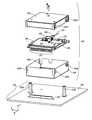
- FIGS. 3A-3Dan example of a pluggable ONU transceiver module 300 is illustrated according to some embodiments of the invention.
- FIG. 3Aillustrates an exploded perspective view
- FIGS. 3B and 3Cillustrate upside-down perspective views
- FIG. 3Dillustrates a side view of the ONU transceiver module 300 .
- the ONU transceiver module 300includes a top shell 302 and a bottom shell 304 configured to mate together to form a cavity. As best seen in FIG. 3A , a PCB 306 is disposed within the cavity, upon which are mounted a triplexer 308 and circuitry 310 that may include a processor or the like.
- the PCB 306further includes a plurality of I/O contacts 312 .
- a plurality of I/O pins 314are coupled to the PCB 306 via the I/O contacts 312 and are configured to be inserted into a protruding socket 316 on a corresponding host device 318 and to electrically connect the ONU transceiver module 300 to the host device 318 .
- the ONU transceiver module 300further includes an optical connector 320 configured to connect to an optical fiber 321 to access an optical network.
- the top shell 302 and bottom shell 304can be secured together using any of a variety of means.
- the top shell 302includes a plurality of protrusions 322 A- 322 D configured to engage complementary openings 324 A- 324 D formed in the bottom shell 304 .
- the top shell 302can be coupled to the bottom shell 304 using one or more screws, bolts, pins, or other fasteners or the like.
- a guiding feature 326is integrated with the bottom shell 304 and is configured to ensure that the plurality of I/O pins 314 are inserted into the correct holes of the protruding socket 316 .
- the guiding feature 326comprises a rectangular opening in the bottom shell 304 that is sized to receive the protruding socket 316 .
- the length of the rectangular opening guiding feature 326can be substantially equal to the length of the protruding socket 316 .
- the I/O pins 314are positioned within the cavity formed by the top shell 302 and bottom shell 304 such that when the rectangular opening guiding feature 326 is aligned with the protruding socket 316 , each of the I/O pins 314 is automatically aligned with the correct hole of the protruding socket 316 . Because the length of the rectangular opening guiding feature 326 is substantially equal to the length of the protruding socket 316 , the I/O pins 314 are substantially constrained to insert into the correct holes of the protruding socket 316 when the protruding socket 316 is inserted into the rectangular opening guiding feature 326 .
- the rectangular opening guiding feature 326allows the protruding socket 316 to be received into the cavity formed by the top shell 302 and bottom shell 304 . In some embodiments, this allows the flat bottom of the bottom shell 304 to rest directly on a PCB 334 of the host device 318 . As such, the bottom shell 304 is configured to prevent the ONU transceiver module 300 from tilting when plugged into the host device 318 .
- the guiding feature 326is disclosed in FIG. 3B as a rectangular opening that is complementary to the shape of the protruding socket 316 , the guiding feature 326 can alternately comprise an opening having a circular, oval, or other shape depending on the shape of the protruding socket 316 .
- an electromagnetic interference (EMI) shield 328is positioned between the PCB 306 and bottom shell 304 to substantially prevent the entrance or exit of electromagnetic radiation (EMR) into or out of the ONU transceiver module 300 .
- EMRelectromagnetic radiation
- the EMI shield 328includes individual openings 330 through which each of the I/O pins 314 extends from the PCB 306 downwards (e.g., towards the bottom shell 304 ).
- the EMI shield 328is configured to substantially prevent EMR from passing through the EMI shield 328 , which EMR might otherwise adversely affect the PCB 306 and electronic/optoelectronic components mounted thereto in the case of externally generated EMR, or that might adversely affect the host device 318 or other devices external to the ONU transceiver module 300 in the case of internally generated EMR.
- the EMI shield 328can be omitted.
- the host device 318includes a plurality of posts 332 A and 332 B mounted on the PCB 334 of the host device 318 .
- Each of the posts 332 A and 332 Bincludes a threaded through hole configured to receive a screw, bolt or other fastener to secure a heatsink (not shown) to the posts 332 A and 332 B.
- the heatsinkis configured to contact the top of the module 300 to dissipate heat away from the module 300 .
- the top of the ONU transceiver module 300is configured to be positioned at a predetermined height H 1 above the PCB 334 of host device 318 when the ONU transceiver module 300 is plugged into the host device 318 .
- the predetermined height H 1extends slightly above the top of the posts 332 A, 332 B.
- the top of the ONU transceiver module 300e.g., the top of top shell 302
- the bottom shell 304can be formed from stamped sheet metal or the like and can be manufactured in a variety of sizes to accommodate a variety of predetermined heights H 1 .
- the size of the bottom shell 304can be varied by selecting a desired value for lower height H 2 ( FIG. 3D ) of the bottom shell 304 , without changing any of the other dimensions of the bottom shell 304 .
- the bottom shell 304serves as one example of a structural implementation of a means for positioning the top of an ONU transceiver module at a predetermined height H 1 above the PCB 334 of host device 318 .
- the bottom shell 304provides an integrated solution for (1) ensuring that I/O pins are inserted correctly into the protruding socket of the host device, (2) preventing tilting of pluggable ONU transceiver modules when plugged into host devices with protruding sockets, and (3) positioning the top of the ONU transceiver module at a predetermined height to contact a heatsink.
- the bottom shell 304is an integrated solution comprising a single component that can be assembled to the rest of the ONU transceiver module 300 in a single step.
- prior art solutionsinclude multiple components that are assembled to the rest of the module in multiple steps.
- the bottom shell 304presents a robust design that is less susceptible to breaking than conventional stepped guiding pins and bottom shells with holes to receive the stepped guiding pins.
- FIGS. 3A-3Ddisclose an integrated solution for the problems described above, embodiments of the invention are not limited to integrated solutions.
- FIGS. 4A-4Cdisclose two other example ONU transceiver modules according to embodiments of the invention. More specifically, FIG. 4A illustrates an exploded perspective view and FIG. 4B illustrates an upside-down perspective view of a second example ONU transceiver module 400 A; FIG. 4C illustrates an exploded perspective view of a third example ONU transceiver module 400 B.
- the ONU transceiver module 400 A of FIGS. 4A and 4Bincludes a top shell 402 and bottom shell 404 configured to mate together to form a cavity. As best seen in FIG. 4A , a PCB 406 is disposed inside the cavity, upon which are mounted a triplexer 408 and circuitry 410 . The PCB 406 further includes a plurality of I/O contacts 412 . A plurality of I/O pins 414 are coupled to the PCB 406 via the I/O contacts 412 and are configured to be inserted into the protruding socket 316 of host device 318 and to electrically connect the ONU transceiver module 400 A to the host device 318 . The ONU transceiver module 400 A additionally includes an optical connector 420 configured to connect to an optical fiber 421 to access an optical network.
- Top shell 402includes a plurality of protrusions 422 A- 422 D configured to engage complementary openings 424 A- 424 D formed in the bottom shell 404 , to thereby secure the top shell 402 to the bottom shell 404 .
- top shell 402can be coupled to bottom shell 404 using one or more screws, bolts, pins, or other fasteners or the like.
- a plurality of guiding features 426 A, 426 Bare integrally formed in the bottom shell 404 and are configured to ensure that the plurality of I/O pins 414 are inserted into the correct holes of the protruding socket 316 .
- the guiding features 426 A, 426 Bcomprise tabs formed by cutting and bending the tabs outwards from the bottom shell 404 .
- the distance between the tabbed guiding features 426 A, 426 Bcan be substantially equal to the length of the protruding socket 316 .
- the I/O pins 414are positioned between the tabbed guiding features 426 A, 426 B such that when the protruding socket 316 is aligned between the tabbed guiding features 426 A, 426 B, each of the I/O pins 414 is automatically aligned with the correct hole of the protruding socket 316 . Because the distance between the tabbed guiding features 426 A, 426 B is substantially equal to the length of the protruding socket 316 , the I/O pins 414 are inserted into the correct holes of the protruding socket 316 when the protruding socket 316 is aligned between the tabbed guiding features 426 A, 426 B.
- the ONU transceiver module 400 Aincludes a plurality of tabbed feet 428 A- 428 D integrated into the bottom shell 404 .
- the tabbed feet 428 A- 428 Dare formed in some embodiments during the formation of openings 424 A- 424 D, as will be understood by those skilled in the art in view of the present disclosure.
- the top of the ONU transceiver module 400 Ae.g., the top of top shell 402
- the top of the ONU transceiver module 400 Ais positioned at a predetermined height above the PCB 334 of host device 318 by top shell 402 to allow proper mating of a heatsink (not shown) secured to posts 332 A, 332 B with the ONU transceiver module 400 A.
- top shell 402can be manufactured in a variety of sizes to accommodate a variety of predetermined heights. The size of the top shell 402 can be varied by selecting a desired thickness for an extension 430 of the top shell 402 , without changing any of the other dimensions of the top shell 402 .
- the top shell 402serves as a second example of a structural implementation of a means for positioning the top of an ONU transceiver module at a predetermined height above the PCB 334 of host device 318 .
- ONU transceiver module 400 Bis similar in some respects to ONU transceiver module 400 A of FIGS. 4A and 4B .
- the ONU transceiver module 400 Bcan include the same bottom shell 404 , PCB 406 , triplexer 408 , circuitry 410 , contacts 412 , I/O pins 414 , optical connector 420 , protrusions 422 A- 422 D, openings 424 A- 424 D, guiding features 426 A, 426 B, and tabbed feet 428 A- 428 D as the ONU transceiver module 400 A of FIGS. 4A and 4B .
- the guiding features 426 A, 426 B and tabbed feet 428 A- 428 D of FIG. 4Censure that the I/O pins 414 are inserted correctly into the protruding socket 316 and prevent the ONU transceiver module 400 B from tilting when plugged into the host device 318 in the same way as the guiding features 426 A, 426 B and tabbed feet 428 A- 428 D of FIGS. 4A and 4B .
- the ONU transceiver module 400 Bincludes a top shell 402 B that is different than the top shell 402 of FIGS. 4A and 4B .
- the top shell 402 B of FIG. 4Clacks the extension 430 of FIGS. 4A and 4B .
- the ONU transceiver module 400 B of FIG. 4Cincludes a separate insert 432 configured to position the top of the ONU transceiver module 400 B at a predetermined height above the PCB 334 of host device 318 to allow proper mating of a heatsink (not shown) secured to posts 332 A, 332 B with the ONU transceiver module 400 B.
- the insert 432can be manufactured in a variety of thicknesses to accommodate a variety of predetermined heights H 1 and can be secured to the top shell 402 B. To position the top of the ONU transceiver module 400 B at a relatively high predetermined height, the insert 432 will be relatively thick. In contrast, to position the top of the ONU transceiver module 400 B at a relatively low predetermined height, the insert 432 will be relatively thin. Accordingly, the insert 432 serves as a third example of a structural implementation of a means for positioning the top of an ONU transceiver module at a predetermined height above the PCB 334 of host device 318 .
- the ONU transceiver modules 400 A and 400 Binclude a bottom shell 404 configured to (1) ensure that I/O pins are inserted correctly into the protruding socket of the host device via guiding features 426 A, 426 B and (2) prevent tilting of pluggable ONU transceiver modules when plugged into host devices with protruding sockets via tabbed feet 428 A- 428 D. Further, the ONU transceiver modules 400 A and 400 B include means for (3) positioning the top of the ONU transceiver module 400 A or 400 B at a predetermined height to contact a heatsink.
Landscapes
- Physics & Mathematics (AREA)
- General Physics & Mathematics (AREA)
- Optics & Photonics (AREA)
- Electromagnetism (AREA)
- Engineering & Computer Science (AREA)
- Computer Networks & Wireless Communication (AREA)
- Signal Processing (AREA)
- Optical Couplings Of Light Guides (AREA)
Abstract
Description
Claims (7)
Priority Applications (2)
| Application Number | Priority Date | Filing Date | Title |
|---|---|---|---|
| US13/652,381US8573860B2 (en) | 2008-11-13 | 2012-10-15 | Pluggable optical network unit transceiver |
| US14/071,511US8967881B2 (en) | 2008-11-13 | 2013-11-04 | Optical network unit transceiver |
Applications Claiming Priority (2)
| Application Number | Priority Date | Filing Date | Title |
|---|---|---|---|
| SG200808465 | 2008-11-13 | ||
| SG200808465-9 | 2008-11-13 |
Related Child Applications (1)
| Application Number | Title | Priority Date | Filing Date |
|---|---|---|---|
| US13/652,381DivisionUS8573860B2 (en) | 2008-11-13 | 2012-10-15 | Pluggable optical network unit transceiver |
Publications (2)
| Publication Number | Publication Date |
|---|---|
| US20100129035A1 US20100129035A1 (en) | 2010-05-27 |
| US8287192B2true US8287192B2 (en) | 2012-10-16 |
Family
ID=42196354
Family Applications (3)
| Application Number | Title | Priority Date | Filing Date |
|---|---|---|---|
| US12/618,504Active2030-10-12US8287192B2 (en) | 2008-11-13 | 2009-11-13 | Optical network unit transceiver |
| US13/652,381ActiveUS8573860B2 (en) | 2008-11-13 | 2012-10-15 | Pluggable optical network unit transceiver |
| US14/071,511ActiveUS8967881B2 (en) | 2008-11-13 | 2013-11-04 | Optical network unit transceiver |
Family Applications After (2)
| Application Number | Title | Priority Date | Filing Date |
|---|---|---|---|
| US13/652,381ActiveUS8573860B2 (en) | 2008-11-13 | 2012-10-15 | Pluggable optical network unit transceiver |
| US14/071,511ActiveUS8967881B2 (en) | 2008-11-13 | 2013-11-04 | Optical network unit transceiver |
Country Status (1)
| Country | Link |
|---|---|
| US (3) | US8287192B2 (en) |
Cited By (1)
| Publication number | Priority date | Publication date | Assignee | Title |
|---|---|---|---|---|
| US20170311474A1 (en)* | 2016-04-24 | 2017-10-26 | Rahi Systems Inc. | Modular server |
Families Citing this family (42)
| Publication number | Priority date | Publication date | Assignee | Title |
|---|---|---|---|---|
| US11294136B2 (en) | 2008-08-29 | 2022-04-05 | Corning Optical Communications LLC | High density and bandwidth fiber optic apparatuses and related equipment and methods |
| US8452148B2 (en) | 2008-08-29 | 2013-05-28 | Corning Cable Systems Llc | Independently translatable modules and fiber optic equipment trays in fiber optic equipment |
| US8027167B2 (en)* | 2009-03-03 | 2011-09-27 | Antec, Inc. | Case cable management |
| US9075216B2 (en) | 2009-05-21 | 2015-07-07 | Corning Cable Systems Llc | Fiber optic housings configured to accommodate fiber optic modules/cassettes and fiber optic panels, and related components and methods |
| EP2443497B1 (en) | 2009-06-19 | 2020-03-04 | Corning Cable Systems LLC | High density and bandwidth fiber optic apparatus |
| US9658419B2 (en)* | 2009-12-07 | 2017-05-23 | Evertz Microsystems Ltd. | Electrical-optical media conversion system |
| US8992099B2 (en)* | 2010-02-04 | 2015-03-31 | Corning Cable Systems Llc | Optical interface cards, assemblies, and related methods, suited for installation and use in antenna system equipment |
| US20110206328A1 (en)* | 2010-02-25 | 2011-08-25 | Emcore Corporation | Optoelectronic module with emi shield |
| US8913866B2 (en) | 2010-03-26 | 2014-12-16 | Corning Cable Systems Llc | Movable adapter panel |
| CA2796221C (en) | 2010-04-16 | 2018-02-13 | Ccs Technology, Inc. | Sealing and strain relief device for data cables |
| US9519118B2 (en) | 2010-04-30 | 2016-12-13 | Corning Optical Communications LLC | Removable fiber management sections for fiber optic housings, and related components and methods |
| US8879881B2 (en) | 2010-04-30 | 2014-11-04 | Corning Cable Systems Llc | Rotatable routing guide and assembly |
| US9075217B2 (en) | 2010-04-30 | 2015-07-07 | Corning Cable Systems Llc | Apparatuses and related components and methods for expanding capacity of fiber optic housings |
| US9279951B2 (en) | 2010-10-27 | 2016-03-08 | Corning Cable Systems Llc | Fiber optic module for limited space applications having a partially sealed module sub-assembly |
| US9116324B2 (en) | 2010-10-29 | 2015-08-25 | Corning Cable Systems Llc | Stacked fiber optic modules and fiber optic equipment configured to support stacked fiber optic modules |
| CA2819235C (en) | 2010-11-30 | 2018-01-16 | Corning Cable Systems Llc | Fiber device holder and strain relief device |
| WO2012106510A2 (en) | 2011-02-02 | 2012-08-09 | Corning Cable Systems Llc | Dense fiber optic connector assemblies and related connectors and cables suitable for establishing optical connections for optical backplanes in equipment racks |
| US8888383B2 (en)* | 2011-05-03 | 2014-11-18 | Avego Technologies General Ip (Singapore) Pte. Ltd. | Active optical cable (AOC) connector having a molded plastic leadframe, an AOC that incorporates the AOC connector, and a method of using an AOC |
| US9008485B2 (en) | 2011-05-09 | 2015-04-14 | Corning Cable Systems Llc | Attachment mechanisms employed to attach a rear housing section to a fiber optic housing, and related assemblies and methods |
| US20120288244A1 (en)* | 2011-05-12 | 2012-11-15 | Ezconn Corporation | Shielding structure for optical sub-assembly for transceivers |
| US20120314989A1 (en)* | 2011-06-09 | 2012-12-13 | Hui-Tsuo Chou | Optical transceiver module |
| AU2012275598A1 (en) | 2011-06-30 | 2014-01-16 | Corning Optical Communications LLC | Fiber optic equipment assemblies employing non-U-width-sized housings and related methods |
| US8953924B2 (en) | 2011-09-02 | 2015-02-10 | Corning Cable Systems Llc | Removable strain relief brackets for securing fiber optic cables and/or optical fibers to fiber optic equipment, and related assemblies and methods |
| WO2013071124A1 (en)* | 2011-11-09 | 2013-05-16 | Aurora Networks, Inc. | Universal host module for a pluggable optical transmitter |
| US9038832B2 (en) | 2011-11-30 | 2015-05-26 | Corning Cable Systems Llc | Adapter panel support assembly |
| US9250409B2 (en) | 2012-07-02 | 2016-02-02 | Corning Cable Systems Llc | Fiber-optic-module trays and drawers for fiber-optic equipment |
| US20140010555A1 (en)* | 2012-07-06 | 2014-01-09 | Alcatel-Lucent Usa Inc. | PON Video Overlay Amplifier Circuit |
| US9042702B2 (en) | 2012-09-18 | 2015-05-26 | Corning Cable Systems Llc | Platforms and systems for fiber optic cable attachment |
| ES2551077T3 (en) | 2012-10-26 | 2015-11-16 | Ccs Technology, Inc. | Fiber optic management unit and fiber optic distribution device |
| CN105099557A (en)* | 2012-11-08 | 2015-11-25 | 青岛海信宽带多媒体技术有限公司 | Optical module and optical device applied to optical module |
| JP6103634B2 (en)* | 2013-02-15 | 2017-03-29 | 日東電工株式会社 | Opto-electric hybrid module |
| US8985862B2 (en) | 2013-02-28 | 2015-03-24 | Corning Cable Systems Llc | High-density multi-fiber adapter housings |
| TW201506476A (en)* | 2013-08-02 | 2015-02-16 | Hon Hai Prec Ind Co Ltd | Photoelectric conversion device |
| CN103532631A (en)* | 2013-10-11 | 2014-01-22 | 成都优博创技术有限公司 | Pluggable GPON ONU (Gigabit Passive Optical Network Optical Network Unit) for local area network switch system |
| US20160028486A1 (en)* | 2014-07-25 | 2016-01-28 | Tellabs Bedford, Inc. | Modular Passive Optical Network Recessed Wall Mounted Optical Network Terminal System |
| WO2017019083A1 (en)* | 2015-07-30 | 2017-02-02 | Hewlett Packard Enterprise Development Lp | Removable module |
| WO2017019084A1 (en)* | 2015-07-30 | 2017-02-02 | Hewlett Packard Enterprise Development Lp | Transceiver module |
| EP3376838B1 (en) | 2015-12-08 | 2020-11-25 | Huawei Technologies Co., Ltd. | Radio remote unit and component thereof |
| CN105572816B (en)* | 2015-12-23 | 2018-01-30 | 宁波环球广电科技有限公司 | multi-channel parallel optical transceiver module |
| BE1026282B1 (en)* | 2018-05-15 | 2019-12-17 | Phoenix Contact Gmbh & Co | Modular system for manufacturing an electronic device |
| CN111596420B (en)* | 2020-05-09 | 2022-12-09 | 武汉光迅科技股份有限公司 | Optical network terminal |
| TWI829550B (en)* | 2022-03-10 | 2024-01-11 | 周暉座 | Optical communication connection device |
Citations (4)
| Publication number | Priority date | Publication date | Assignee | Title |
|---|---|---|---|---|
| US6180874B1 (en)* | 1997-04-10 | 2001-01-30 | International Business Machines Corporation | High density heatsink attachment and method therefor |
| US6948864B2 (en)* | 2003-09-16 | 2005-09-27 | Agilent Technologies, Inc. | Optoelectronic component with thermoelectric temperature control |
| US7048452B2 (en)* | 2003-11-10 | 2006-05-23 | Jds Uniphase Corporation | Transceiver guide rail with heat sink guide |
| US20070253667A1 (en)* | 2004-03-23 | 2007-11-01 | Herbert Brunner | Optoelectronic Component with Multi-Part Housing Body |
Family Cites Families (5)
| Publication number | Priority date | Publication date | Assignee | Title |
|---|---|---|---|---|
| IT1247304B (en)* | 1991-04-30 | 1994-12-12 | Sgs Thomson Microelectronics | CIRCUIT POWER MODULAR STRUCTURE COMPLEX WITH HIGH COMPACTNESS AND HIGH THERMAL DISSIPATION EFFICIENCY |
| US5990776A (en)* | 1994-12-08 | 1999-11-23 | Jitaru; Ionel | Low noise full integrated multilayers magnetic for power converters |
| US6856769B1 (en)* | 2000-10-24 | 2005-02-15 | Infineon Technologies Ag | Optical transceiver module |
| US8160451B2 (en)* | 2007-02-13 | 2012-04-17 | Finisar Corporation, Inc. | Optical network unit transceiver module with arrayed I/O video contacts |
| US7651341B2 (en)* | 2008-04-02 | 2010-01-26 | Hon Hai Precision Ind. Co., Ltd. | Circuit board assembly with staggered cable arrangement |
- 2009
- 2009-11-13USUS12/618,504patent/US8287192B2/enactiveActive
- 2012
- 2012-10-15USUS13/652,381patent/US8573860B2/enactiveActive
- 2013
- 2013-11-04USUS14/071,511patent/US8967881B2/enactiveActive
Patent Citations (4)
| Publication number | Priority date | Publication date | Assignee | Title |
|---|---|---|---|---|
| US6180874B1 (en)* | 1997-04-10 | 2001-01-30 | International Business Machines Corporation | High density heatsink attachment and method therefor |
| US6948864B2 (en)* | 2003-09-16 | 2005-09-27 | Agilent Technologies, Inc. | Optoelectronic component with thermoelectric temperature control |
| US7048452B2 (en)* | 2003-11-10 | 2006-05-23 | Jds Uniphase Corporation | Transceiver guide rail with heat sink guide |
| US20070253667A1 (en)* | 2004-03-23 | 2007-11-01 | Herbert Brunner | Optoelectronic Component with Multi-Part Housing Body |
Cited By (2)
| Publication number | Priority date | Publication date | Assignee | Title |
|---|---|---|---|---|
| US20170311474A1 (en)* | 2016-04-24 | 2017-10-26 | Rahi Systems Inc. | Modular server |
| US10757829B2 (en)* | 2016-04-24 | 2020-08-25 | Rahi Systems Inc. | Modular server |
Also Published As
| Publication number | Publication date |
|---|---|
| US8967881B2 (en) | 2015-03-03 |
| US20100129035A1 (en) | 2010-05-27 |
| US20130044985A1 (en) | 2013-02-21 |
| US20140064677A1 (en) | 2014-03-06 |
| US8573860B2 (en) | 2013-11-05 |
Similar Documents
| Publication | Publication Date | Title |
|---|---|---|
| US8967881B2 (en) | Optical network unit transceiver | |
| US8160451B2 (en) | Optical network unit transceiver module with arrayed I/O video contacts | |
| US8328435B2 (en) | Printed circuit board positioning spacers in an optoelectronic module | |
| KR100840691B1 (en) | Modular Optical Device Packages | |
| US8708575B2 (en) | Active optical connector using audio port | |
| US20180267263A1 (en) | Optical module with integrated lens | |
| US9588307B2 (en) | Parallel optical transceiver with top and bottom lenses | |
| US7331720B1 (en) | Transceiver module for optical communications and method for transmitting and receiving data | |
| US8920048B2 (en) | Communications module with a shell assembly having thermal mechanical features | |
| US20110268390A1 (en) | Active optical cable that is suited for consumer applications and a method | |
| US20060088254A1 (en) | Surface mount (SMT) connector for VCSEL and photodiode arrays | |
| CN103293607A (en) | Pluggable optical transceiver | |
| US10514510B2 (en) | Optical component assembly having a keyed structure for ensuring proper insertion orientation within an optical subassembly | |
| US9103999B2 (en) | Optical data communication module having EMI cage | |
| US6632030B2 (en) | Light bending optical block for fiber optic modules | |
| US9011024B2 (en) | Optical communication module and assembling method thereof | |
| US20150098680A1 (en) | Optically connecting a chip package to an optical connector | |
| US8613559B2 (en) | Universal serial bus connector | |
| US7396166B1 (en) | Optical transceiver module | |
| US8731347B2 (en) | Lens standoff and protection for optical communication systems | |
| US8636426B2 (en) | Photoelectric conversion system with optical transceive module | |
| US20200400899A1 (en) | High density optical transceiver assembly | |
| US9081158B2 (en) | Optical fiber connector | |
| KR20190009664A (en) | Active optical cable |
Legal Events
| Date | Code | Title | Description |
|---|---|---|---|
| AS | Assignment | Owner name:FINISAR CORPORATION, CALIFORNIA Free format text:ASSIGNMENT OF ASSIGNORS INTEREST;ASSIGNOR:TEO, TAT MING;REEL/FRAME:023893/0722 Effective date:20091230 | |
| STCF | Information on status: patent grant | Free format text:PATENTED CASE | |
| FPAY | Fee payment | Year of fee payment:4 | |
| AS | Assignment | Owner name:BANK OF AMERICA, N.A., AS ADMINISTRATIVE AGENT, NO Free format text:NOTICE OF GRANT OF SECURITY INTEREST IN PATENTS;ASSIGNORS:II-VI INCORPORATED;MARLOW INDUSTRIES, INC.;EPIWORKS, INC.;AND OTHERS;REEL/FRAME:050484/0204 Effective date:20190924 Owner name:BANK OF AMERICA, N.A., AS ADMINISTRATIVE AGENT, NORTH CAROLINA Free format text:NOTICE OF GRANT OF SECURITY INTEREST IN PATENTS;ASSIGNORS:II-VI INCORPORATED;MARLOW INDUSTRIES, INC.;EPIWORKS, INC.;AND OTHERS;REEL/FRAME:050484/0204 Effective date:20190924 | |
| AS | Assignment | Owner name:II-VI DELAWARE, INC., DELAWARE Free format text:ASSIGNMENT OF ASSIGNORS INTEREST;ASSIGNOR:FINISAR CORPORATION;REEL/FRAME:052286/0001 Effective date:20190924 | |
| MAFP | Maintenance fee payment | Free format text:PAYMENT OF MAINTENANCE FEE, 8TH YEAR, LARGE ENTITY (ORIGINAL EVENT CODE: M1552); ENTITY STATUS OF PATENT OWNER: LARGE ENTITY Year of fee payment:8 | |
| AS | Assignment | Owner name:JPMORGAN CHASE BANK, N.A., AS COLLATERAL AGENT, NEW YORK Free format text:SECURITY INTEREST;ASSIGNORS:II-VI INCORPORATED;II-VI DELAWARE, INC.;M CUBED TECHNOLOGIES, INC.;AND OTHERS;REEL/FRAME:060562/0254 Effective date:20220701 | |
| AS | Assignment | Owner name:PHOTOP TECHNOLOGIES, INC., CALIFORNIA Free format text:PATENT RELEASE AND REASSIGNMENT;ASSIGNOR:BANK OF AMERICA, N.A., AS ADMINISTRATIVE AGENT;REEL/FRAME:060574/0001 Effective date:20220701 Owner name:II-VI OPTOELECTRONIC DEVICES, INC., NEW JERSEY Free format text:PATENT RELEASE AND REASSIGNMENT;ASSIGNOR:BANK OF AMERICA, N.A., AS ADMINISTRATIVE AGENT;REEL/FRAME:060574/0001 Effective date:20220701 Owner name:II-VI DELAWARE, INC., PENNSYLVANIA Free format text:PATENT RELEASE AND REASSIGNMENT;ASSIGNOR:BANK OF AMERICA, N.A., AS ADMINISTRATIVE AGENT;REEL/FRAME:060574/0001 Effective date:20220701 Owner name:II-VI PHOTONICS (US), INC., MASSACHUSETTS Free format text:PATENT RELEASE AND REASSIGNMENT;ASSIGNOR:BANK OF AMERICA, N.A., AS ADMINISTRATIVE AGENT;REEL/FRAME:060574/0001 Effective date:20220701 Owner name:M CUBED TECHNOLOGIES, INC., CONNECTICUT Free format text:PATENT RELEASE AND REASSIGNMENT;ASSIGNOR:BANK OF AMERICA, N.A., AS ADMINISTRATIVE AGENT;REEL/FRAME:060574/0001 Effective date:20220701 Owner name:II-VI OPTICAL SYSTEMS, INC., CALIFORNIA Free format text:PATENT RELEASE AND REASSIGNMENT;ASSIGNOR:BANK OF AMERICA, N.A., AS ADMINISTRATIVE AGENT;REEL/FRAME:060574/0001 Effective date:20220701 Owner name:FINISAR CORPORATION, CALIFORNIA Free format text:PATENT RELEASE AND REASSIGNMENT;ASSIGNOR:BANK OF AMERICA, N.A., AS ADMINISTRATIVE AGENT;REEL/FRAME:060574/0001 Effective date:20220701 Owner name:OPTIUM CORPORATION, CALIFORNIA Free format text:PATENT RELEASE AND REASSIGNMENT;ASSIGNOR:BANK OF AMERICA, N.A., AS ADMINISTRATIVE AGENT;REEL/FRAME:060574/0001 Effective date:20220701 Owner name:COADNA PHOTONICS, INC., PENNSYLVANIA Free format text:PATENT RELEASE AND REASSIGNMENT;ASSIGNOR:BANK OF AMERICA, N.A., AS ADMINISTRATIVE AGENT;REEL/FRAME:060574/0001 Effective date:20220701 Owner name:KAILIGHT PHOTONICS, INC., CALIFORNIA Free format text:PATENT RELEASE AND REASSIGNMENT;ASSIGNOR:BANK OF AMERICA, N.A., AS ADMINISTRATIVE AGENT;REEL/FRAME:060574/0001 Effective date:20220701 Owner name:LIGHTSMYTH TECHNOLOGIES, INC., OREGON Free format text:PATENT RELEASE AND REASSIGNMENT;ASSIGNOR:BANK OF AMERICA, N.A., AS ADMINISTRATIVE AGENT;REEL/FRAME:060574/0001 Effective date:20220701 Owner name:EPIWORKS, INC., ILLINOIS Free format text:PATENT RELEASE AND REASSIGNMENT;ASSIGNOR:BANK OF AMERICA, N.A., AS ADMINISTRATIVE AGENT;REEL/FRAME:060574/0001 Effective date:20220701 Owner name:MARLOW INDUSTRIES, INC., TEXAS Free format text:PATENT RELEASE AND REASSIGNMENT;ASSIGNOR:BANK OF AMERICA, N.A., AS ADMINISTRATIVE AGENT;REEL/FRAME:060574/0001 Effective date:20220701 Owner name:II-VI INCORPORATED, PENNSYLVANIA Free format text:PATENT RELEASE AND REASSIGNMENT;ASSIGNOR:BANK OF AMERICA, N.A., AS ADMINISTRATIVE AGENT;REEL/FRAME:060574/0001 Effective date:20220701 | |
| MAFP | Maintenance fee payment | Free format text:PAYMENT OF MAINTENANCE FEE, 12TH YEAR, LARGE ENTITY (ORIGINAL EVENT CODE: M1553); ENTITY STATUS OF PATENT OWNER: LARGE ENTITY Year of fee payment:12 |