US8285387B2 - Wireless communication with a medical implant - Google Patents
Wireless communication with a medical implantDownload PDFInfo
- Publication number
- US8285387B2 US8285387B2US12/334,196US33419608AUS8285387B2US 8285387 B2US8285387 B2US 8285387B2US 33419608 AUS33419608 AUS 33419608AUS 8285387 B2US8285387 B2US 8285387B2
- Authority
- US
- United States
- Prior art keywords
- radiating element
- metal surface
- reactive
- radiating
- antenna
- Prior art date
- Legal status (The legal status is an assumption and is not a legal conclusion. Google has not performed a legal analysis and makes no representation as to the accuracy of the status listed.)
- Expired - Fee Related, expires
Links
Images


Classifications
- A—HUMAN NECESSITIES
- A61—MEDICAL OR VETERINARY SCIENCE; HYGIENE
- A61N—ELECTROTHERAPY; MAGNETOTHERAPY; RADIATION THERAPY; ULTRASOUND THERAPY
- A61N1/00—Electrotherapy; Circuits therefor
- A61N1/18—Applying electric currents by contact electrodes
- A61N1/32—Applying electric currents by contact electrodes alternating or intermittent currents
- A61N1/36—Applying electric currents by contact electrodes alternating or intermittent currents for stimulation
- A61N1/372—Arrangements in connection with the implantation of stimulators
- A61N1/37211—Means for communicating with stimulators
- A61N1/37217—Means for communicating with stimulators characterised by the communication link, e.g. acoustic or tactile
- A61N1/37223—Circuits for electromagnetic coupling
- H—ELECTRICITY
- H01—ELECTRIC ELEMENTS
- H01Q—ANTENNAS, i.e. RADIO AERIALS
- H01Q1/00—Details of, or arrangements associated with, antennas
- H01Q1/27—Adaptation for use in or on movable bodies
- H01Q1/273—Adaptation for carrying or wearing by persons or animals
- H—ELECTRICITY
- H01—ELECTRIC ELEMENTS
- H01Q—ANTENNAS, i.e. RADIO AERIALS
- H01Q1/00—Details of, or arrangements associated with, antennas
- H01Q1/12—Supports; Mounting means
- H01Q1/22—Supports; Mounting means by structural association with other equipment or articles
- H01Q1/2208—Supports; Mounting means by structural association with other equipment or articles associated with components used in interrogation type services, i.e. in systems for information exchange between an interrogator/reader and a tag/transponder, e.g. in Radio Frequency Identification [RFID] systems
- H01Q1/2241—Supports; Mounting means by structural association with other equipment or articles associated with components used in interrogation type services, i.e. in systems for information exchange between an interrogator/reader and a tag/transponder, e.g. in Radio Frequency Identification [RFID] systems used in or for vehicle tyres
- H—ELECTRICITY
- H01—ELECTRIC ELEMENTS
- H01Q—ANTENNAS, i.e. RADIO AERIALS
- H01Q1/00—Details of, or arrangements associated with, antennas
- H01Q1/36—Structural form of radiating elements, e.g. cone, spiral, umbrella; Particular materials used therewith
- H01Q1/38—Structural form of radiating elements, e.g. cone, spiral, umbrella; Particular materials used therewith formed by a conductive layer on an insulating support
- H—ELECTRICITY
- H01—ELECTRIC ELEMENTS
- H01Q—ANTENNAS, i.e. RADIO AERIALS
- H01Q21/00—Antenna arrays or systems
- H01Q21/30—Combinations of separate antenna units operating in different wavebands and connected to a common feeder system
- H—ELECTRICITY
- H01—ELECTRIC ELEMENTS
- H01Q—ANTENNAS, i.e. RADIO AERIALS
- H01Q5/00—Arrangements for simultaneous operation of antennas on two or more different wavebands, e.g. dual-band or multi-band arrangements
- H01Q5/40—Imbricated or interleaved structures; Combined or electromagnetically coupled arrangements, e.g. comprising two or more non-connected fed radiating elements
- H—ELECTRICITY
- H01—ELECTRIC ELEMENTS
- H01Q—ANTENNAS, i.e. RADIO AERIALS
- H01Q9/00—Electrically-short antennas having dimensions not more than twice the operating wavelength and consisting of conductive active radiating elements
- H01Q9/04—Resonant antennas
- H01Q9/0407—Substantially flat resonant element parallel to ground plane, e.g. patch antenna
- H01Q9/0414—Substantially flat resonant element parallel to ground plane, e.g. patch antenna in a stacked or folded configuration
Definitions
- This inventionrelates to medical implants, and more particularly to communication with a medical implant.
- the known medical implantsare those that either receive information from a transmitter outside the body or transmit information to a receiver located outside the body. Such communication is most conveniently carried out by causing electromagnetic waves to propagate between an intra-corporal medical implant and an extra-corporal base station.
- a difficulty with the use of electromagnetic wavesarises from their tendency to be attenuated when traveling within the human body. Although attenuation decreases with increasing wavelengths, the use of longer wavelengths typically requires the use of large antennas.
- the United States Federal Communication Commission (“FCC”)allocated the Medical Implant Communication Service (“MICS”) band, which extends between 402 MHz and 405 MHz, as available for use by medical implants.
- MICSMedical Implant Communication Service
- the MICS bandrepresents an attempt at compromise, it is still the case that body tissues significantly attenuate electromagnetic waves propagating at MICS frequencies.
- the distance between the base station and the implantmust be small.
- the base station's receiving antennais placed on or within inches of the skin.
- the inventionis based on the recognition that a non-omnidirectional antenna on a medical implant will interact with the patient's body in such a way as to yield a nearly omnidirectional radiation pattern.
- the inventionfeatures an apparatus for providing transdermal wireless communication.
- the apparatusincludes medical implant circuitry, a transceiver coupled to the medical implant circuitry, a first metal surface having an end portion and a base portion, a second metal surface parallel to the first metal surface and connected to the first metal surface by a conductor, and separated from the first metal surface by a dielectric layer, a first radiating element tuned to a first frequency and disposed within the dielectric layer between the first metal surface and second metal surface.
- the first radiating elementhas a first reactive portion at a first end thereof, a second reactive portion at a second end thereof, and a first radiating strip extending between the first reactive portion and the second reactive portion.
- the apparatusfurther includes a feed structure in electrical communication with the transceiver and the first radiating strip.
- the first reactive portionincludes a first capacitive structure
- the second reactive portionincludes a second capacitive structure
- the first reactive portionincludes a first conductive planar portion having a dimension in excess of a width of the first radiating strip
- the second reactive portionincludes a second conductive planar portion having a dimension in excess of the width of the first radiating strip
- Alternative embodimentsinclude those in which the first reactive portion includes an inductive structure, and those in which the first reactive portion includes a first conducting strip disposed to follow a first serpentine path, and the second reactive portion includes a second conducting strip disposed to follow a second serpentine path, as well as those in which the first reactive portion of the first radiating element includes an inductive structure and the second reactive portion includes a capacitive structure.
- Yet other embodimentsinclude those in which the feed structure is separated from the first radiating strip by a dielectric, and those in which the feed structure is capacitively coupled to the first radiating strip.
- inventionsinclude a second radiating element tuned to a second frequency and disposed between the first reactive portion of the first radiating element and the second reactive portion of the first radiating element.
- the feed structurecan provide a signal of the first frequency and a signal of the second frequency to both the first radiating element and the second radiating element.
- the feed structureis capacitively coupled to both the first radiating element and the second radiating element.
- the second radiating elementis tuned to a frequency between approximately 2 GHz and 2.5 GHz.
- planar surfaceforms the second metal surface.
- the planar surfaceincludes a surface of a housing.
- inventionsinclude those in which the second metal surface includes a planar surface of a housing.
- the end portion of the first metal surfaceis disposed over the first reactive portion of the first radiating element and the base portion of the first metal surface is disposed over the second reactive portion of the first radiating element.
- inventionsinclude those in which the first radiating element defines a region at which an electric field supported by the first radiating element has its maximum amplitude, and in which at least one of the end portion and base portion is disposed over the defined region, those in which at least one of the end portion and base portion is disposed over a region at which a gradient vector of electric field amplitude reverses direction, those in which at least one of the end portion and base portion is disposed to intercept electric field lines in a region at which an electric field supported by the first radiating element reaches its maximum amplitude, and those in which at least one of the end portion and base portion is disposed to block a selected portion of an electric field supported by the first radiating element, with examples of the selected portion of the electric field including a portion having an amplitude in excess of a threshold, and a portion having a gradient vector that reverses direction.
- Additional embodimentsinclude those in which the first radiating element is tuned to a first frequency within the MICS band, and those in which the first radiating element is tuned to a first frequency between 400 MHz and 405 MHz.
- At least one embodiment of the apparatusfurther includes a neck extending between the end portion and the base portion.
- inventionsinclude those in which at least one of the first metal surface and the second metal surface includes a planar surface, those in which the first and second metal surfaces include grounded surfaces, and those in which the first and second metal surfaces include ground planes.
- the inventionfeatures an apparatus for providing transdermal wireless communication in a selected direction, the apparatus including medical implant circuitry; a transceiver coupled to the medical implant circuitry; and a first metal surface disposed in a plane perpendicular to the selected direction.
- the first metal surfacehas an end portion, and a base portion.
- the apparatusfurther includes a first planar radiating element tuned to a first frequency and disposed on a dielectric layer above the first metal surface, the first planar radiating element having a first reactive portion at a first end thereof, a second reactive portion at a second end thereof, and a first planar radiating strip extending between the first reactive portion and the second reactive portion; and a feed structure in electrical communication with the transceiver and the first planar radiating strip for providing the carrier signal to the first planar radiating strip.
- the apparatusfurther includes a neck extending between the end portion and the base portion.
- the inventionfeatures an apparatus for providing wireless communication across the skin of a patient, the apparatus including: medical implant circuitry; a transceiver coupled to the medical implant circuitry; a feed configured to receive a signal from the transceiver; a planar radiating element coupled to the feed; and a field stop disposed to block radiation from selected portions of an electric field distribution supported by the planar radiating element.
- Another aspect of the inventionis a method for providing transdermal communication, the method including causing a current on an antenna implanted inside a patient, the antenna supporting an electromagnetic field having a near-field component and a far-field component; shielding the near-field component, thereby trapping energy contained in the near-field component and reducing the extent to which the energy in the near-field component interacts with the patient; and allowing the propagation of the far-field component through the skin of the patient.
- shielding the near-field componentincludes placing a conductive plane between a reactive portion of the antenna and the skin
- shielding the near-field componentincludes placing a conductive plane over a first end of the antenna and a second end of the antenna
- those that further include selecting the antenna to be a radiating stripinclude those in which shielding the near-field component includes placing a conductive plane between a reactive portion of the antenna and the skin.
- Another aspect of the inventionis a method of providing wireless communication between a medical implant and a base station across the skin of a patient in the presence of a mismatch between the permittivity of the patient's skin layer and the permittivity of a medium surrounding the patient.
- Such a methodincludes communicating with a transceiver of a medical implant that has been implanted under the skin of a patient; causing an antenna on the medical implant to launch an electromagnetic wave carrying energy, the energy having a first portion traveling in a first direction and a second portion traveling in a direction other than the first direction, the first and second portions having different magnitudes, wherein a portion of the first portion enters a layer of the patient and causes an endoperipheral wave that propagates within the peripheral layer, and wherein as the endoperipheral wave propagates within the peripheral layer, a portion of the energy carried by the endoperipheral wave exits the endoperipheral layer and enters a surrounding medium, the ratio of the portion of the energy that exits the skin layer
- Yet another aspect of the inventionfeatures a method of providing wireless communication between a medical implant in a patient and a base station.
- Such a methodincludes causing an antenna on the medical implant to launch a wave having a first portion in a first direction and a second portion in a second direction, the first and second portions having differing magnitudes, wherein a portion of the first portion enters a biological waveguide defined by a constituent of the body of the patient, the biological waveguide having a first permittivity that differs from the permittivity of the medium surrounding the base station; whereby the wave launched into the biological waveguide becomes a guided wave having an energy, and wherein as the guided wave propagates in the biological waveguide, a portion of the energy escapes the biological waveguide and enters the medium surrounding the base station; and wherein the ratio of energy escaping the biological waveguide to the energy remaining in the biological waveguide depends on the ratio between the permittivity of the biological waveguide and the permittivity of the medium surrounding the base station.
- the biological waveguideincludes a portion of the skin.
- Another aspect of the inventionfeatures a method of determining a preferred patient orientation for establishing communication between a medical implant inside a patient and a base station outside the patient.
- Such a methodincludes, following the healing of an incision caused by implantation of a medical implant inside a patient, determining an angle between an implant axis of the implant and a patient axis of the patient; on the basis of the angle, determining an optimal orientation of the patient relative to the base station for establishing wireless communication between the medical implant and the base station; and providing, to the patient, information representative of the optimal orientation.
- the inventionfeatures an apparatus for providing energy to first and second antennas.
- the apparatusincludes a first section of a microstrip transmission line, the first section extending from a feedpoint along an axis; a first load for coupling to the first antenna, the first load being connected to a distal end of the first section; a second section of microstrip transmission line, the second section extending along the axis and having a proximal end connected to the first pair of microstrip transmission line stubs; and a second load connected to a distal end of the second section for coupling to the second antenna; wherein the lengths of the first and second sections are selected to cause an electromagnetic wave having a first frequency to encounter an impedance mismatch at the first load and an impedance match at the second load, and to cause an electromagnetic wave having a second frequency to encounter an impedance mismatch at the second load and an impedance match at the first load.
- the inventionfeatures an apparatus for providing energy to first and second antennas.
- the apparatusincludes a first section of a microstrip transmission line, the first section extending from a feedpoint along an axis; a first load for coupling to the first antenna, the first load being connected to a distal end of the first section; a second section of microstrip transmission line extending from the feedpoint and along a direction parallel to and offset from the axis; and a second load for coupling to the second antenna, the second section being connected to a distal end of the second section; wherein the lengths of the first and second sections are selected to cause an electromagnetic wave having a first frequency to encounter an impedance mismatch at the first load and an impedance match at the second load, and to cause an electromagnetic wave having a second frequency to encounter an impedance mismatch at the second load and an impedance match at the first load.
- the apparatusincludes a third section of microstrip transmission line extending from the feedpoint and along a direction parallel to and offset from the axis and offset from the second section, and a third load for coupling to the second antenna, the third section being connected to a distal end of the third section; wherein the lengths of the first, second, and third sections are selected to cause an electromagnetic wave having a first frequency to encounter an impedance mismatch at the first load and an impedance match at the second and third loads, and to cause an electromagnetic wave having a second frequency to encounter an impedance match at the first load and an impedance mismatch at the second and third loads.
- FIG. 1shows a medical implant in communication with a base station
- FIG. 2shows the medical implant of FIG. 1 in more detail
- FIG. 3is a block diagram of the wireless communication system of the medical implant of FIG. 2 ;
- FIG. 4is a flow chart of a communication protocol carried out by the base station of FIG. 1 ;
- FIG. 5is a flow chart of a communication protocol carried out by the wireless communication system of FIG. 3 ;
- FIG. 6shows the dissipation of energy associated with a conventional omnidirectional antenna
- FIG. 7shows the propagation of endodermal waves associated with the antenna associated with the wireless communication system of FIG. 3 ;
- FIG. 8is a transverse cross section of the medical implant shown in FIG. 2 ;
- FIG. 9is an exploded isometric view of the antenna system shown in FIG. 8 ;
- FIG. 10is a detailed view of the radiating archipelago of the antenna shown in FIG. 8 ;
- FIG. 11is a detailed view of the top ground plane of the antenna shown in FIG. 8 ;
- FIG. 12is an alternative to the radiating archipelago shown in FIG. 10 , in which the reactive portions provide an inductance rather than a capacitance;
- FIG. 13shows an alternative to the radiating archipelago of FIG. 10 ;
- FIG. 14shows details of the feed structure shown in FIG. 9 ;
- FIGS. 15A and 15Bshow matching circuits from FIG. 3 ;
- FIG. 16shows an antenna feed thru for feeding the antenna of FIG. 9 ;
- FIG. 17shows a process for forming a dielectric layer on the antenna system shown in FIG. 8 ;
- FIG. 18shows a structure for providing capacitive coupling between an antenna and a feed
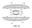
- FIG. 19shows an alternate embodiment of the radiating archipelago of FIG. 13 ;
- FIGS. 20 and 21show additional embodiments of a feed structure for the antenna system shown in FIG. 9 ;
- FIGS. 22 and 23show representative three-dimensional patterns for the antenna system of FIG. 8 ;
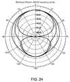
- FIGS. 24 and 25show representative slices through the three-dimensional patterns shown in FIGS. 22 and 23 ;
- FIGS. 26 and 27show antenna gain for antennas that have been implanted in a piece of meat.
- FIG. 1shows a medical implant 10 , sometimes referred to as an “implantable medical device,” in a patient 12 .
- the medical implant 10is one that either performs actions in response to instructions, transmits data, or both.
- the medical implant 10could be one that releases drugs in response to a stimulus.
- An example of an implant for controlled release or exposure of the contents of an implanted reservoiris described in U.S. Patent Pub. 2004/0121486 (Uhland et al.), entitled “Controlled Release Device and Method Using Electrothermal Ablation,” the contents of which are herein incorporated by reference.
- the medical implant 10could be one that performs physiological measurements, such as measuring glucose levels, cardiac signals, or blood pressure levels.
- One implant for measuring glucoseis that disclosed in U.S. Patent Pub. 2005/0096587 (Santini), entitled “Medical Device for Sensing Glucose,” the contents of which are incorporated herein by reference.
- the term “medical implant”refers to active implantable medical devices.
- An “active implantable medical device”is a medical device that uses electricity or other energy, and is partly or totally inserted into a human or animal body or a natural orifice by means of a surgical or medical procedure, and is typically expected to remain there for several days, weeks, months, or years after the procedure is completed.
- the term “medical device”refers to a manufactured product that is used to prevent, diagnose, treat, or monitor human or animal disease or injuries, or to investigate, replace, modify, or maintain anatomical structures or physiological functions. Manufactured products that achieve results by pharmacological, immunological, or metabolic means are not medical devices. However, the results achieved by medical devices may be assisted by these means.
- medical implants suitable for use in/with the present antenna devices and telemetry methodsinclude pacemakers, cardioverter-defibrillators, nerve and muscle stimulators, deep brain stimulators, drug delivery devices (e.g., drug pumps), cardiomyostimulators, cochlear implants, artificial organs (e.g., artificial hearts), biological sensors, and cardiac and other physiologic monitors.
- the medical implantmay provide of a combination of these functionalities.
- the medical implantcomprises a multi-reservoir containment device for the controlled in vivo exposure or release of reservoir contents, as described for example in U.S. Pat. No. 6,527,762 (Santini et al.), U.S. Pat. No.
- the wireless linkit is generally useful to provide such medical implants 10 with a wireless link to a base station 14 located near the patient 12 .
- the wireless linkit is useful for the wireless link to be such that the patient 12 may stray a limited distance from the base station 14 without interrupting communication. This would enable the wireless link to be used unobtrusively. For example, if the range of the wireless link is on the order of the size of a typical household room, such as a bedroom, or a typical hospital room, and if radiation exits the patient 12 omnidirectionally, it is possible for the patient 12 to be anywhere within the room without disrupting wireless communication between the implant 10 and the base station 14 .
- omnidirectionaland “omnidirectionally” are used to describe receiving or sending radio waves equally well in all directions in a principal plane of an antenna.
- the term “equally well”is not intended to imply strict and unvarying equality but is intended to encompass minor deviations from equality.
- FIG. 2shows the medical implant 10 in more detail.
- the medical implant 10features a generally elliptical housing 15 having a major axis 16 .
- the housing 15is typically a biocompatible metal, such as titanium or titanium alloy shell, with the metal forming the shell having a wall thickness of about 0.3 mm.
- the overall thickness of the housing 15is 8.2 mm.
- the overall thickness of the housing 15is 10-11 mm.
- An elliptical locking ring 18having similar transverse dimensions as the housing 15 holds an RF transparent cover or dielectric shield 20 in place above an antenna structure (not shown) connected to a transceiver (not shown).
- the cover 20functions to protect the antenna structure from contact with bodily fluids and/or tissues.
- the locking ring 18is typically a biocompatible metal, such as titanium.
- a suitable material for an RF-transparent cover 20 or dielectric shieldis non-conducting material, such as polyethylene, having a thickness of about 0.4 mm. Alternately, one could fill the space with a biocompatible epoxy, which would then be the cover 20 .
- orientation of the major axis 16 in a direction parallel to the patient's spineresults in an omnidirectional pattern in a plane transverse to the patient's spine.
- This configurationis thus preferable for signal transmission.
- it may be more comfortable for the patient 12if the surgeon were to orient the major axis 16 inside the patient 12 in a direction perpendicular to the patient's spine.
- the deviceIn practice, once the device is implanted, it may shift to another orientation. Thus, as a practical matter it may be difficult to precisely control the orientation of the medical implant 10 . It is therefore desirable that the overall operation of the communication system be relatively independent of the implant's orientation.
- the implant 10may shift its orientation after surgery, one can compensate for any such shift. For example, once the incision has healed, it is possible to determine the orientation of the implant 10 . This can be achieved, for example, by X-ray inspection, or by rotating the receiving antenna to identify a radiation maximum. If the implant 10 is sufficiently close to the skin, the orientation can be determined by feeling the implant 10 through the skin. In either case, one can then determine an optimal orientation of the implant 10 relative to the base station 14 for establishing communication with the base station 14 . Information representative of this optimal orientation can then be made available for the patient's use in guiding his activities, or for optimally arranging a patient's furnishings, such as the bed and the base station 14 , to maximize likelihood of establishing and maintaining such communication while the patient is asleep.
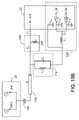
- FIG. 3is a block diagram of the medical implant 10 showing a transceiver 22 having MICS circuitry 24 for communication in the MICS band, and wake-up circuitry 26 for providing a wake up signal to the MICS circuitry 24 .
- Both the MICS circuitry 24 and the wake up circuitry 26are in communication, through matching circuits 27 , 29 A, 29 B, with a dual band antenna 28 as described in more detail in connection with FIGS. 4 and 5 .
- a controller 30provides control over both the MICS circuitry 24 and the wake-up circuitry 26 .
- Implant circuitry 32controls the functions of an implant device 33 .
- a suitable transceiver 22is the ZL70101 manufactured by Zarlink Semiconductor of Ottawa, Ontario, which is in widespread commercial use in the U.S. and other countries.
- the base station 14 and transceiver 22communicate through two frequency bands: a lower frequency band, such as the MICS band, which extends from 402-405 MHz, and a higher frequency band having frequencies on the order of 2.45 GHz.
- the MICS bandis used primarily for data communication between the transceiver 22 and the base station 14 , whereas the higher frequency band is used to provide a wake-up signal to the transceiver 22 , but it is not necessary that the transceiver 22 transmit back to the base station 14 at the 2.45 GHz frequency.
- FIG. 4summarizes a procedure used by the base station 14 to establish communication with a medical implant 10 .
- the base station 14transmits a wake up signal at 2.45 GHz (step 34 ) and then listens for a response on a MICS frequency (step 36 ).
- This wake up signalincludes information identifying the particular MICS frequencies to be used. If no response is forthcoming, the base station 14 retransmits the wake up signal (step 34 ). If the base station 14 detects a response from the implant, it then establishes communication in the MICS band with the implant 10 (step 38 ).
- the transceiver 22 on the implant 10carries out a procedure such as that shown in FIG. 5 .
- the wake-up circuitry 26 of the implant's transceiver 22periodically listens for a wake up signal at 2.45 GHz (step 40 ). If no signal is detected (step 42 ), the controller 30 instructs the wake up circuitry 26 to wait for some pre-selected interval (step 44 ) and repeats this process (step 40 ). Otherwise, if the transceiver 22 detects a wake up signal (step 42 ), it sends a signal to wake up the MICS circuitry 24 (step 46 ) which then establishes communication with the base station 14 (step 48 ). In one embodiment, the waiting time is selected to be approximately one minute. In another embodiment, the controller 30 causes the wake-up circuitry 26 to listen for the base station 14 at a particular time. In yet another embodiment, the controller 30 causes the wake-up circuitry 26 to listen for the base station 14 at variable time intervals.
- the communication protocol described in FIGS. 4 and 5is particularly advantageous because the 2.45 GHz signal can be repeatedly broadcast by the base station 14 at relatively high power, and because the wake-up circuitry 26 on the medical implant does not have to consume power by transmitting. Moreover, there is no need to power up the MICS circuitry 24 unless MICS communication is actually required. In addition, since the wake-up signal identifies the portion of the MICS band to be used, there is no need for the MICS circuitry 24 to consume energy scanning across the MICS band to search for a signal.
- a difficulty that arises when attempting to communicate with an implanted transceiver 22is that the tissues that make up the human body generally have complex permittivity.
- the imaginary term of a complex permittivityresults in evanescent waves.
- Evanescent wavesare essentially waves that die away, or decay, with distance from their sources. Such waves cannot be used to carry data over any meaningful distance since they themselves cannot travel any meaningful distance.
- FIG. 6shows a prior art implant 50 located near the ventral surface 52 (i.e., the belly or stomach) of a patient 12 .
- the implant 10uses a conventional antenna that radiates omnidirectionally in a transverse plane.
- the power that actually leaves the patient's body in a particular directiondepends on the path length that the wave must traverse within the body, and the permittivities that the wave encounters before reaching free space.
- a wave 54 traveling in a ventral directionexperiences little attenuation because the path length before reaching free space is relatively short.
- a wave 56 traveling in the dorsal directioni.e., toward the spine or back
- an antenna 28 as shown in FIG. 7provides a beam core 58 directed radially outward, away from the patient's core, and a beam periphery 60 directed to cause energy to enter the patient's peripheral layer 62 .
- peripheral layerrefers to the outermost layers of the body. Accordingly, “peripheral layer” may include the dermal layer and other tissues found in the outermost layers, such as subcutaneous fats, as well as the integumentary layer.
- the peripheral layer 62has a permittivity that differs from both the free space permittivity and from the permittivity of the interior 64 of the patient's body. As such, it functions in the manner of a leaky waveguide.
- the antenna 28is believed to launch an electromagnetic wave within the peripheral layer 62 . Since the wave propagates in the peripheral layer 62 , it will be referred to herein as an “endoperipheral wave.” As it propagates, the endoperipheral wave encounters two discontinuities in permittivity that define the inner and outer boundaries of the peripheral layer 62 . When the endoperipheral wave is incident on the outer boundary, a portion of its energy leaks across the boundary and propagates in free space. The remaining portion is reflected back and continues to propagate endoperipherally.
- the net effect of the foregoing arrangement as shown in FIG. 7is a reduction in the dramatically different path lengths shown in FIG. 6 .
- the combination of the antenna 28 and the human body shown in FIG. 7radiates in a more omnidirectional manner than the combination shown in FIG. 6 , as shown in FIGS. 22 and 23 .
- the conventional antenna shown in FIG. 6is an omnidirectional antenna.
- the antenna 28 shown in FIG. 7is not an omnidirectional antenna; it is a directional antenna.
- a directional antenna in a medical implant 10would fail to achieve a nearly omnidirectional pattern.
- the directional antenna 28interacts in an unexpected way with the patient's anatomy so that even though the antenna 28 itself is directional, the synergy between the directional antenna 28 and the wave propagation properties of the patient's anatomy results in a nearly omnidirectional radiation pattern for the overall system formed by the antenna 28 and the patient 12 , as shown in FIGS. 22 and 23 .
- FIG. 8shows a transverse cross section of a medical implant 10 having an antenna 28 for launching electromagnetic waves in the manner described above.
- the medical implant 10has a housing 15 on which is disposed a bottom ground plane 66 separated from a top ground plane 68 by a conducting connector 70 .
- the top ground plane 68 and the bottom ground plane 66may also be referred to as “field stops,” “shields,” or more generally, as a “metal surfaces,” which may or may not be planar, and which may or may not be grounded.
- the transceiver 22which transmits information from the body to a base station 14 outside the body or receives information from a base station 14 outside the body.
- the transceiver 22communicates with implant circuitry 32 that controls operation of an implant device 33 that interacts with the body.
- implant device 33is a glucose sensor as disclosed by U.S. Patent Pub. 2005/0096587 (Santini), referred to above, which is hereby incorporated by reference.
- Other examples of implant devices 33include those that perform physiological measurements and those for releasing various drugs.
- a radiating archipelago 72comprising planar, non-wire radiating structures.
- a feed structure 74 disposed between the bottom ground plane 66 and the radiating archipelago 72is connected to the transceiver 22 disposed within the housing 15 .
- the feed structure 74 , top and bottom ground planes 66 , 68 , radiating archipelago 72 , and the connector 70 and related structuresform the antenna 28 .
- Transceiver 22 , implant circuitry 32 , and implant device 33are sealed within the housing 15 . Signals are passed into and out of the housing 15 between transceiver 22 and antenna 28 using a feed-through structure 160 , which is described in more detail in connection with FIG. 16 .
- top and bottom ground planes 68 , 60are separated by a dielectric material, best seen in the exploded view of FIG. 9 .
- a first dielectric layer 76separates the bottom ground plane 66 from the feed structure 74 .
- a second dielectric layer 78separates the feed structure 74 from the radiating archipelago 72 .
- a third dielectric layer 80separates the radiating archipelago 72 from the top ground plane 68 .
- a bottom dielectric cover 77isolates the bottom ground plane 66 from contact with any adjacent conducting media.
- a top dielectric cover 79isolates the top ground plane 68 from any adjacent conducting media.
- the top and bottom ground planes 68 , 60are connected by one or more connectors 70 , not shown in FIG. 9 , that pass through the various dielectric layers.
- the connectors 70can typically be vias or metal pins.
- the radiating archipelago 72is capacitively coupled to the feed structure 74 and to the top ground plane 68 .
- the first dielectric layer 76is the thickest of the three.
- the second and third dielectric layers 78 , 80are of approximately equal thickness and significantly thinner than the first dielectric layer 76 .
- the exact thicknesses of each layerdepend on the properties of the dielectric and on the wavelengths to be used by the antenna 28 .
- the first dielectric layer 76has a thickness of 1.27 mm and the second and third dielectric layers 78 , 80 each have a thickness of 0.1 mm.
- the thicknesses of the dielectric layers 76 , 78 , 80 required for optimal radiation characteristicsare particularly sensitive to the dielectric's permittivity.
- the permittivity of a dielectricvaries about some nominal permittivity value from one lot or batch of material from which a dielectric layer is formed to the next lot or batch from which a dielectric layer is formed. Although the variations about the nominal value are small, and may be unimportant in many applications, in the present application such errors are likely to make a significant difference in the performance of the antenna 28 .
- a suitable dielectric materialis a biocompatible material having a high dielectric constant, which tends to reduce the overall dimensions of the antenna.
- the dielectric materialis alumina having a relative permittivity of 9.5 ⁇ 10% such as that supplied by DuPont under trade designation QM44.
- QM44relative permittivity
- the antenna 28In an effort to promote uniformity in manufacture, it is useful to inspect data provided by the manufacturer concerning the measured permittivity of a particular lot of dielectric.
- the dielectric layers 76 , 86 , 80are formed by repeatedly painting and curing individual laminas of dielectric material to build up a layer of dielectric 76 , 86 , 80 having the desired thickness.
- the correct number of laminas required to build up a dielectric layer 76 , 86 , 80 having the desired thicknesscan then provide the manufacturing facility with instructions concerning the correct number of laminas.
- a process for attaining a desired capacitanceincludes receiving, from the manufacturer, a lot or batch of particular dielectric (step 174 ) and a measured value of a permittivity associated with that lot.
- the processthen includes retrieving the desired capacitance (step 178 ) and the thickness “d” of a typical lamina of cured dielectric that would be laid down by a particular manufacturing process (step 180 ). In a typical screen-printing process, this thickness d would correspond to the screen thickness.
- a value of n, the number of laminas having thickness d required to attain capacitance Cis then obtained, either by calculation or by use of a look-up table (step 182 ).
- the resulting value, n, of the number of laminasis then output (step 184 ) and provided to a manufacturing facility.
- the manufacturing facilitythen forms the requisite number of laminas to build up a layer of thickness d (step 186 ) and then forms a feed structure on top of the layer 76 thus formed (step 188 ).
- a similar processcan be used to build up the second layer 78 and the third layer 80 .
- each laminaIn many practices, the thickness of each lamina is constant. However, in some practices of the manufacturing process, the individual laminas have different thicknesses. In such cases, the individual thicknesses are made to sum to the desired thickness.
- FIG. 10shows the radiating archipelago 72 in detail.
- the radiating archipelago 72is made up of twin MICS radiators 82 , 84 that are mirror images of each other.
- the first MICS radiator 82includes a radiative portion 86 extending between first and second reactive portions 88 , 90 at opposite ends thereof.
- the radiative portion 86is formed by two generally parallel radiating strips 92 , 94 that extend between the first reactive portion 88 at one end of the first MICS radiator 82 and the second reactive portion 90 at the other end of the first MICS radiator 82 .
- the second MICS radiator 84includes a radiative portion 96 extending between first and second reactive portions 98 , 100 at opposite ends thereof.
- the radiative portion 96is formed by two generally parallel radiating strips 102 , 104 that extend between the first reactive portion 98 at one end of the second MICS radiator 84 and the second reactive portion 100 at the other end of the second MICS radiator 84 .
- These radiative strips 102 , 104carry out a function similar to a wire antenna.
- the radiative strips 92 , 94 , 102 , 104are essentially two-dimensional structures that can easily be formed using planar processing techniques.
- FIG. 11shows a top ground plane 68 in more detail.
- the top ground plane 68includes an enlarged base portion 106 that is connected to the bottom ground plane 66 by one or more connectors 70 through a via.
- vias and connectors 70are located away from the radiative portions 86 , 96 of the first and second MICS radiators 82 , 84 .
- At the opposite end of the top ground plane 68is an enlarged end portion 108 connected to the base portion 106 by an optional neck 110 .
- the neck 110is disposed to shield surrounding tissues from stray electric fields generated by the feed structure 74 .
- the base portion 106is positioned to cover the reactive portions 88 , 98 on one end of the twin MICS radiators 82 , 84 .
- the end portion 108is positioned to cover the remaining two reactive portions 90 , 100 on the opposite end of the twin MICS radiators 82 , 84 .
- the particular shapes of the end and base portions 106 , 108are not critical to their overall function.
- the end portion 108 of the top ground plane 68 and the two reactive portions 90 , 100 of the MICS radiators 82 , 84lie on opposite sides of the third dielectric layer 80 . As such, they collectively define a first capacitor 112 between them, as shown in FIG. 8 .
- the base portion 106 of the top ground plane 68 and the two remaining reactive portions 88 , 98also lie on opposite sides of the third dielectric layer 80 . As such, they collectively form a second capacitor 114 , shown in FIG. 8 .
- Each of these capacitors 112 , 114entraps electric field lines, thus suppressing the tendency of the antenna's near field to heat or to otherwise be dissipated by the human tissue adjacent to the implant 10 .
- the energy in the near fieldis available to oscillate from one end of the MICS radiators 82 , 84 to the other, preferably at a resonance frequency associated with the MICS radiators 82 , 84 . As a result, this energy can contribute more significantly to far-field radiation.
- Waves that ultimately reach the far field of the antenna 28originate primarily from the radiative portions 86 , 96 . Since these radiative portions lie underneath and on opposite sides of the neck 110 of the top ground plane 68 , there is little to impede wave propagation from these portions. In embodiments that lack any neck, nothing at all impedes wave propagation. As a result, those waves are free to propagate into the far field of the antenna 28 .
- the “far field” of an antennais used in a manner consistent with the way it is used in the antenna arts.
- the “far field”is the region of space that is so remote from the antenna that the electromagnetic field of the antenna, which normally includes an evanescent component and a radiating component, consists primarily of the radiating component.
- an antenna 28 as described hereinprovides a pattern having a main lobe 58 that radiates energy in a radial direction away from the patient 12 .
- some of the energy stored in the near field at the ends of the MICS radiators 82 , 84escapes through the gap between the top and bottom ground planes 66 , 68 .
- This energyis manifested as side lobes 60 shown in FIG. 7 . It is these side lobes 60 that are believed to provide the energy for launching the endodermal wave.
- An antenna 28 as described abovehas a relatively low radiation efficiency, i.e. only a small portion of energy delivered to the radiative portions 86 , 96 is actually radiated. The bulk of the energy remains stored in the near field of the antenna 28 rather than being radiated away.
- the transceiver 22provides energy through a feed point 116 , best seen in FIGS. 8 and 14 .
- the energypropagates along the feed structure 74 and couples capacitively to the radiative portions 86 , 96 .
- the energytravels towards the reactive portions 90 , 100 .
- a small portion of that energyradiates from the relatively inefficient radiating strips 92 , 94 , 102 , 104 of the radiative portions 86 , 96 .
- the bulk of the energyreaches the reactive portions 90 , 100 and reflects back to travel again along the radiative portions 86 , 96 , where another small portion radiates away.
- the remainderthen proceeds to the opposite reactive portion 88 , 98 , which then reflects it back along the radiative portions 86 , 96 .
- the reactive portions 90 , 100 , 88 , 98 and radiative portions 86 , 96thus cooperate to cause energy to oscillate back and forth between the reactive portions 90 , 100 , 88 , 98 .
- a small portion of that energyradiates away as it traverses the radiative portions 86 , 96 .
- the minimal energy radiated with each oscillationaccumulates and eventually provides sufficient power to communicate with a base station 14 located at some distance away. For example it is believed that this arrangement will permit communication within the same room approximately five meters away.
- the operation of the antenna 28thus provides another unexpected result. Ordinarily, one would expect to increase range by increasing efficiency, i.e., by providing an antenna 28 that has high radiation resistance. This would translate into a greater fraction of energy being radiated in the far field of the antenna 28 . While this may be the desirable solution in free space, the limited space within the human body makes it difficult to implant a large enough antenna to have a high radiation resistance in the MICS band. However, implanting a small antenna with low radiation resistance causes more energy to be retained in the antenna's near field. Since the antenna near field lies within human tissue, this results in dielectric losses.
- the reactive portions 90 , 100 , 88 , 98are shielded by the top ground plane 68 .
- the shieldingconstrains near fields from spilling out into the surrounding tissue. As a result, dielectric loss is reduced.
- the antenna 28 described hereinis a highly inefficient antenna, i.e., one with a low radiation resistance.
- a highly inefficient antennaonly an insignificant fraction of energy provided to the antenna actually radiates into the far field. Nevertheless, by entrapping the bulk of the energy and bleeding it into the far field a little bit at a time through relatively inefficient radiative portions 86 , 96 , the antenna 28 avoids losses arising from interaction between its near field and surrounding human tissue. This leads to the unexpected result of an inefficient antenna 28 that nevertheless manages to provide long range wireless communication between a medical implant 10 and a base station as much as 5 meters away.
- the antenna 28is analogous to a laser oscillator, in which light oscillates between two mirrors with only a small portion of the light escaping through a half-silvered mirror with each oscillation.
- the antenna 28can be viewed as an RLC circuit in which the resonant frequency, which is the reciprocal of the square root of the product of the effective inductance and capacitance, is within the desired frequency band of operation, i.e. the MICS band.
- the relatively small radiation resistance, as well as the inductance,is provided by the radiative portions 86 , 96 .
- the capacitance, which dominates the illustrated configuration,is provided by the two capacitors 112 , 114 formed by the interaction between the reactive portions 100 , 88 , 90 , 98 of the MICS radiators 82 , 84 and the base and end portions 106 , 108 of the top ground plane 68 .
- the RLC circuitis dominated by inductance rather than capacitance.
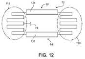
- the reactive portions of the MICS radiators 82 , 84are meander line structures 118 , 120 such as those shown in FIG. 12 .
- the radiating strips 122 , 124are made somewhat wider so that they can provide the necessary capacitance to tune the antenna 28 .
- the transceiver 22operates on two frequencies: one in the MICS band and another, in the UHF band, for carrying the wake-up signal.
- UHFmeans one of the ISM (Industrial, Scientific, Medical) bands, and specifically, the ISM band that includes frequencies between 2.4 GHz and 2.5 GHz.
- an alternative embodiment of the radiating archipelago 72 shown in FIG. 13features UHF radiators 126 , 128 tuned to resonate at 2.45 GHz, as shown in FIG. 10 .
- the UHF radiators 126 , 128are twin radiating elements, each one being an essentially linear structure.
- the first UHF radiator 126has a first reactive portion 130 and a second reactive portion 132 connected by a radiative portion 138 extending between them.
- the second UHF radiator 128has a first reactive portion 134 and a second reactive portion 136 connected by a radiative portion 140 extending between them.
- the use of the term “radiative” portionis not intended to imply that the structure can be used only for transmitting electromagnetic waves.
- antennasare subject to reciprocity. Hence, structures used for transmitting waves have the same properties when used for receiving electromagnetic waves.
- the radiative portions 138 , 140 of the first and second UHF radiators 126 , 128are formed into radiative strips like those shown on the MICS radiators 82 , 84 .
- the neck 110can include a central neck 142 and two peripheral necks 144 , 146 , with each peripheral neck 144 , 146 connecting the central neck 142 to one of the end portion 108 and base portion 106 .
- the peripheral necks 144 , 146are both wider than the central neck 142 , but not so wide as to interfere with propagation of waves escaping from the radiative portions 82 , 84 of the MICS radiators. However, the peripheral neck portions 144 , 146 are nevertheless wide enough to form a pair of capacitors with the reactive portions 130 , 132 , 134 , 136 of the twin UHF radiators 126 , 128 .
- the top ground plane 68has: (1) a central neck 142 having a length of 4 mm and a width of 1.1 mm; and (2) a pair of 5.1 mm wide peripheral necks 144 , 146 having lengths of 6.85 mm long and 10.45 mm respectively.
- the base portion 106 of the top ground plane 68is a semicircular region having a radius of 9 mm.
- the end portion 108is a semicircular region having a radius of 9 mm contiguous with a rectangular region extending 4 mm towards the base portion 106 and 17.8 mm along a direction perpendicular to the major axis 16 of the implant 10 .
- a bottom ground plane 66 corresponding to the above top ground plane 68is a rectangular region extending 25.2 mm along the major axis 16 and 18.82 mm perpendicular to the major axis 16 .
- Each 18.82 mm side of the rectangular regionis contiguous with a semicircular region having a radius of approximately 9.4 mm.
- the feed structure 74is an axial transmission line 143 extending from the feed point 116 along the major axis 16 .
- a distal load 145formed by two short sections 147 , 149 of transmission line extending perpendicularly from the axial transmission line 143 in opposite directions underneath the reactive portions 88 , 98 of the MICS radiators 82 , 84 .
- an intermediate load 150formed by an additional pair of transmission line sections 152 , 154 extending perpendicularly from the axial transmission lines 143 .
- a distal section 148 of the axial transmission line 143extends between the distal load 145 and the intermediate load 150 .
- a proximal section 141 of the axial transmission line 143extends between the intermediate load 150 and the feed point 116 .
- a suitable diplexing feed structure 74 for the radiating archipelago 72whose numerical dimensions have been provided features a distal section 148 having a length of approximately 16.75 mm, and a proximal section 141 having a length of approximately 11.24 mm.
- the axial transmission line 143 , the intermediate load 150 and the distal load 145cooperate to form a diplexing feed structure 74 , or diplexer.
- diplexing feed structure 74makes it possible to use a single coaxial cable instead of a pair of coaxial cables to provide energy to the feed structure 74 . This is particularly advantageous where the device is one in which space is at a premium, for example in a medical implant 10 .
- the use of a diplexing feed structure 74is by no means mandatory for operation of the antenna 28 .
- the antenna 28can also be excited by two separate coaxial cables or other transmission lines carrying signals in two different frequency bands.
- a suitable diplexing feed structure 74 for the radiating archipelago 72whose numerical dimensions have been provided features an axial transmission line 143 extending 31.5 mm between the feedpoint 116 and the distal load 145 .
- a pair of 1 mm wide transmission line sections 152 , 154 extending 3 mm on either side of the axial transmission line 142provides the intermediate load 150 .
- a pair of transmission line sections 147 , 152 2.5 mm wide extending 1.35 mm on either side of the axial transmission line 143provides the distal load 144 .
- an axial transmission line 200extends along the axis 16 of the implant 10 between the feed point 116 and a distal load 202 formed by a pair of transmission line stubs 204 , 206 extending perpendicular to the axial transmission line 200 in opposite directions.
- the distal load 202is disposed to capacitively couple with the MICS radiators 82 , 84 .
- Also extending from the feed point 116are a pair of transmission lines 208 parallel to and offset from the axial transmission line 200 .
- Each of the pair of transmission lines 208ends at an intermediate load 210 that capacitively couples to one of the UHF radiators 134 , 136 .
- an additional loadis provided by introducing a tuning stub formed by proximal and distal right-angle bends in the axial transmission line 143 .
- These two right-angle bendsare connected by a connecting section of transmission line parallel to but offset from the axial transmission line 143 .
- the connecting sectionin one embodiment is 1 mm long and offset by 1.5 mm from the axial transmission line 143 .
- the proximal right-angle bendis approximately 23.7 mm from the feedpoint 116
- the distal right-angle bendis an additional 1 mm further from the feedpoint 116 .
- a wave formed by the superposition of an MICS component and a UHF componentoriginates at the feed point 116 and propagates along the axial transmission line 142 .
- the impedance as seen by the UHF componentis such that the distal load 145 appears as an open or short circuit, whereas the intermediate load 150 is matched to the UHF radiators 134 , 136 .
- the UHF componentis effectively coupled into the UHF radiators 134 , 136 and rejected by the MICS radiators 82 , 84 .
- the impedance as seen by the MICS componentis such that the intermediate load 150 appears as an open or short circuit and the distal load 145 is matched to the MICS radiators 82 , 84 .
- the MICS componentis effectively coupled to the MICS radiators 82 , 84 and rejected by the UHF radiators 134 , 136 .
- the impedancesare neither those of short circuits nor of open circuits.
- the impedancesinclude a finite and non-zero imaginary (i.e., reactive) component.
- the reactive componentis capacitive; however, for certain configurations the reactive component is inductive.
- the feed structure 74is disposed in its own layer between the radiating archipelago 72 and the bottom ground plane 66 .
- a disadvantage of this configurationis that it requires an additional metal layer, and thereby complicates manufacturing.
- the feed structure 74 and the radiating archipelago 72are on the same dielectric layer.
- the feed structure 74is directly connected to selected portions of the radiating archipelago 72 rather than being capacitively coupled to those portions. Such a configuration is less sensitive to errors in manufacture since there is no longer a need to rely on capacitive coupling between the feed structure 74 and the radiating archipelago 72 .
- FIG. 18shows UHF radiators 126 , 128 capacitively coupled to the feed point 116 using planar capacitors 127 formed by interdigitating conductive traces 129 connected to the UHF radiators 126 , 128 with conductive traces 131 connected to the feed point 116 .
- the radiating archipelago 72extends 15.3 mm from an outermost edge of one outer radiating strip 92 of one MICS radiator 82 to an outermost edge of an outer radiating strip 102 of the other MICS radiator 84 , and 36.9 mm from the tip of one reactive portion 88 to the other reactive portion 90 .
- Each radiating stripis about 1.5 mm wide and 21.2 mm long.
- Each pair of radiating strips 102 , 104is separated by a gap of approximately 0.44 mm.
- Each UHF radiator 126 , 128has a radiative portion 138 approximately 3.9 mm long and 1 mm wide.
- Each UHF radiator 126has reactive portions 130 , 134 at each end, with the reactive portions 130 , 134 being formed by a metal strip approximately 2.8 mm long and 1 mm wide extending in a direction perpendicular to the radiative portion 138 .
- the overall electrical length of the MICS radiators 82 , 84amounts to an insignificant fraction of a wavelength.
- FIG. 15Ashows one embodiment of a matching circuit 27 to match the transceiver 22 to the antenna 28 .
- the transceiver 22has an input impedance in the UHF band of 2 kilo-ohms, and an input impedance in the MICS band of 500 ohms when transmitting and 20 kilo-ohms when receiving.
- the antenna 28has a 50 ohm input impedance.
- a coaxial cable 156 with characteristic impedance of 50 ohmsconnects the antenna 28 to the matching circuit 27 .
- the illustrated matching circuit 27features two paths, one for each band.
- a first pathconnects the transceiver 22 directly to the antenna 28 by way of coupling capacitor C 1 .
- a second pathuses a coupling capacitor C 2 and coupling inductor L 2 to connect the transceiver 22 to the antenna 28 by way of an LC circuit 158 made up of inductor L 1 in parallel with capacitor C 3 .
- This second pathis tuned by a variable shunt capacitor CV.
- coupling capacitor C 1has a capacitance of approximately 0.5 picofarads
- coupling capacitor C 2has a capacitance of between about 0.5 and 5 picofarads
- coupling inductor L 2has a value between 15 nH and 50 nH, and preferably at or near 22 nH
- the variable capacitance C vhas a capacitance ranging from 5 to 60 picofarads.
- the LC circuit in this embodimentincludes a capacitance C 3 of approximately 1 picofarad and an inductance L 1 of approximately 3 nanohenries.
- the matching circuit 27 of FIG. 15Bfeatures two paths, one for each band.
- a first pathconnects the 2.45 GHz receiving port (RX_UHF) of the transceiver 22 directly to the antenna 28 using a coupling capacitance C 1 in series with a high-pass filter 226 formed by a capacitance C 2 and inductance L 1 .
- a second pathuses a stop-band filter 224 formed by capacitor C 3 in parallel with inductor L 2 in series with a pi-matching network 228 .
- the pi-matching network 228is formed by an inductor L 3 having one terminal connected to ground by a capacitor C 5 internal to the chip housing the transceiver 22 and another terminal connected to ground by a DC coupling capacitance C 4 in series with parallel capacitors C TX and C RX , both of which are also internal to the transceiver 22 .
- the capacitor C TX , a transmission port TX-RF of the transceiver 22 by an amplifier TX and the capacitor C RXis coupled to a receiving port RX-RF of the transceiver 22 by an amplifier RX.
- a feed-through 160provides a connection between the coaxial cable 156 and the antenna 28 . This allows the circuit components to be sealed within housing 15 and the antenna 28 to be placed on an external surface of the housing 15 .
- the RF transparent cover 20can be made of simple construction to keep the antenna 28 clear of body fluids.
- the location of the feed-through 160 relative to the matching circuit 27is shown schematically in FIGS. 15A and 15 B.
- the feed-through 160includes an annulus 162 having an outer rim 164 and an inner rim 166 .
- the annulus 162is sized so that the outer rim 164 engages the sides of a hole in the bottom ground plane 66 at the feed point 116 , as shown in FIG. 8 .
- a dielectric plug 168 shown in FIG. 16fills the space defined by the inner rim 166 .
- First and second conductors 170 , 172extend through the dielectric plug 168 .
- the first conductor 170extends to the feed structure 74 while the second conductor 172 contacts the bottom ground plane 66 . In this way, the feed-through 160 provides electrical contact between the antenna 28 and the matching circuit 27 .
- FIGS. 22 and 23show simulated three-dimensional radiation patterns for the antenna at 403.5 MHz (in the MICS band) and at 2.45 GHz respectively.
- the patternswere computed using the finite-element method as implemented by HFSS software provided by Ansoft Corporation of Pittsburgh, Pa.
- the y-axiscorresponds to the major axis 16 of the housing 15
- the z-axiscorresponds to the direction away from the patient's body
- the ⁇ z directioncorresponds to a direction into the patient's body.
- at each bandthere exist nulls in the direction of the major axis and an approximately omnidirectional pattern in a plane transverse to the major axis 16 of the housing 15 .
- there exists a small amount of loss in the ⁇ z directionthat arises as a result of dielectric and conductive losses in the layer amount of tissue that is traversed in that direction.
- a link budgetwas prepared.
- a constraint imposed on the link budgetwas that for any direction within 40 degrees of the antenna beam's maximum, the power available at the base station 14 would be at least ⁇ 90.1 dBm when the transmitted power was ⁇ 3 dBm.
- the link budgetassumed a ⁇ 1 dBm loss in the matching circuit and a ⁇ 2.7 dBm loss for transmission in a direction of forty degrees off-axis. Transmission across five meters was assumed to result in another ⁇ 39 dBm loss.
- a fading margin of ⁇ 5 dBwas assumed in the link budget to account for multipath interference between the antenna and the base station.
- the receiving antennawas assumed to have a 0 dB gain and a matching circuit loss of ⁇ 1 dB.
- An antenna as described hereinwas implanted beneath a layer of fat in pig meat.
- An antenna gain in the on-axis directionwas then measured at frequencies between 360 MHz and 440 MHz in an anechoic chamber using a first antenna under approximately one inch of fat, and using the first antenna and a second antenna under approximately half an inch of fat.
- the resulting on-axis gains as a function of frequencyare shown in FIG. 26 .
- the on-axis gain at 403.4 MHzwas approximately ⁇ 24 to ⁇ 25 dB.
- the power that entered the transceiver 22 following a ⁇ 3 dBm transmission in a direction 40 degrees off-axis across five meters of free spacewas found to be adequate for reliable communication.
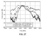
- An antenna as described hereinwas implanted beneath a half inch layer of fat in pig meat.
- An on-axis antenna gainwas then determined in an anechoic chamber by sweeping across a frequency band extending between 2.25 GHz and 2.60 GHz using a first antenna under approximately one inch of fat, and using the first antenna and a second antenna under approximately half an inch of fat.
- the resulting on-axis gains as a function of frequencyare shown in FIG. 27 .
- the on-axis antenna gain at 2.45 GHzwas between approximately ⁇ 16 dB and ⁇ 18 dB.
- the resulting power available at the transceiver 22 following a 21 dBm transmission from a base station 14 in a direction forty degrees off-axis across five meters of free spacewas found to be sufficient to reliably detect a wake-up signal at the transceiver 22 .
Landscapes
- Physics & Mathematics (AREA)
- Electromagnetism (AREA)
- Health & Medical Sciences (AREA)
- Life Sciences & Earth Sciences (AREA)
- Engineering & Computer Science (AREA)
- Biomedical Technology (AREA)
- Nuclear Medicine, Radiotherapy & Molecular Imaging (AREA)
- Radiology & Medical Imaging (AREA)
- Acoustics & Sound (AREA)
- Animal Behavior & Ethology (AREA)
- General Health & Medical Sciences (AREA)
- Public Health (AREA)
- Veterinary Medicine (AREA)
- Electrotherapy Devices (AREA)
- Measuring And Recording Apparatus For Diagnosis (AREA)
- Prostheses (AREA)
Abstract
Description
- 10 medical implant
- 12 patient
- 14 base station
- 15 housing of implant
- 16 major axis of implant
- 18 locking ring on housing
- 20 RF-transparent cover
- 22 transceiver
- 24 MICS circuitry
- 26 wake-up circuitry
- 27 matching circuit
- 28 antenna
- 29A,29B matching circuits (internal to transceiver)
- 30 controller
- 32 implant circuitry
- 33 implant device
- 50 medical implant
- 52 ventral surface of patient
- 54 wave traveling ventrally
- 56 wave traveling dorsally
- 58 main lobe of antenna
- 60 side lobe of antenna
- 62 dermal layer
- 64 interior of patient
- 66 bottom ground plane
- 68 top ground plane
- 70 connector between top and bottom ground planes
- 72 radiating archipelago
- 74 feed structure
- 76,78,80 dielectric layers
- 77,79 dielectric covers
- 82,84 MICS radiators
- 86,96 radiative portions of MICS radiators
- 88,90,98,100 reactive portion of MICS radiators
- 92,94,102,104 radiative strips of MICS radiators
- 106 base portion of top ground plane
- 108 end portion of top ground plane
- 110 neck of top ground plane
- 112 first capacitor
- 114 second capacitor
- 116 feed point
- 118,120 meanderline structures
- 122,124 radiative strips of meanderline antenna
- 126,128 UHF radiators
- 127 planar capacitor
- 129,131 conductive traces of planar capacitor
- 130,132,134,136 reactive portions of UHF radiators
- 138,140 radiative portions of UHF radiators
- 141 proximal section of axial transmission line
- 142 central neck portion of top shield
- 143 axial transmission line
- 144,146 peripheral neck portions of top shield
- 145 distal load
- 147,149 distal load transmission line stubs
- 148 distal section of axial transmission line
- 150 intermediate load
- 152,154 intermediate load transmission line stubs
- 156 coaxial cable
- 158 LC circuit
- 160 feed through
- 162 frame of feed through
- 164 outer rim of frame
- 166 inner rim of frame
- 168 dielectric plug
- 170 first conductor
- 172 second conductor
- 200 axial transmission line
- 202 distal load
- 204,206 transmission line stubs
- 208 transmission lines
- 210 intermediate load
- 215 axial transmission line
- 218 distal load
- 220 intermediate load
- 222 transmission
- 224 stop-band filter
- 226 high-pass filter
- 228 pi-matching network
Claims (30)
Priority Applications (4)
| Application Number | Priority Date | Filing Date | Title |
|---|---|---|---|
| US12/334,196US8285387B2 (en) | 2008-12-12 | 2008-12-12 | Wireless communication with a medical implant |
| EP09771459AEP2374183A2 (en) | 2008-12-12 | 2009-12-11 | Wireless communication with a medical implant |
| PCT/US2009/067637WO2010068846A2 (en) | 2008-12-12 | 2009-12-11 | Wireless communication with a medical implant |
| US13/610,394US8718787B2 (en) | 2008-12-12 | 2012-09-11 | Wireless communication with a medical implant |
Applications Claiming Priority (1)
| Application Number | Priority Date | Filing Date | Title |
|---|---|---|---|
| US12/334,196US8285387B2 (en) | 2008-12-12 | 2008-12-12 | Wireless communication with a medical implant |
Related Child Applications (1)
| Application Number | Title | Priority Date | Filing Date |
|---|---|---|---|
| US13/610,394DivisionUS8718787B2 (en) | 2008-12-12 | 2012-09-11 | Wireless communication with a medical implant |
Publications (2)
| Publication Number | Publication Date |
|---|---|
| US20100149042A1 US20100149042A1 (en) | 2010-06-17 |
| US8285387B2true US8285387B2 (en) | 2012-10-09 |
Family
ID=41559639
Family Applications (2)
| Application Number | Title | Priority Date | Filing Date |
|---|---|---|---|
| US12/334,196Expired - Fee RelatedUS8285387B2 (en) | 2008-12-12 | 2008-12-12 | Wireless communication with a medical implant |
| US13/610,394Expired - Fee RelatedUS8718787B2 (en) | 2008-12-12 | 2012-09-11 | Wireless communication with a medical implant |
Family Applications After (1)
| Application Number | Title | Priority Date | Filing Date |
|---|---|---|---|
| US13/610,394Expired - Fee RelatedUS8718787B2 (en) | 2008-12-12 | 2012-09-11 | Wireless communication with a medical implant |
Country Status (3)
| Country | Link |
|---|---|
| US (2) | US8285387B2 (en) |
| EP (1) | EP2374183A2 (en) |
| WO (1) | WO2010068846A2 (en) |
Cited By (86)
| Publication number | Priority date | Publication date | Assignee | Title |
|---|---|---|---|---|
| US20150255858A1 (en)* | 2014-03-05 | 2015-09-10 | Pacesetter, Inc. | Systems and methods for a dual band antenna for an internal medical device |
| US9526909B2 (en) | 2014-08-28 | 2016-12-27 | Cardiac Pacemakers, Inc. | Medical device with triggered blanking period |
| US9592391B2 (en) | 2014-01-10 | 2017-03-14 | Cardiac Pacemakers, Inc. | Systems and methods for detecting cardiac arrhythmias |
| US9669230B2 (en) | 2015-02-06 | 2017-06-06 | Cardiac Pacemakers, Inc. | Systems and methods for treating cardiac arrhythmias |
| US9694189B2 (en) | 2014-08-06 | 2017-07-04 | Cardiac Pacemakers, Inc. | Method and apparatus for communicating between medical devices |
| US9757570B2 (en) | 2014-08-06 | 2017-09-12 | Cardiac Pacemakers, Inc. | Communications in a medical device system |
| US9808631B2 (en) | 2014-08-06 | 2017-11-07 | Cardiac Pacemakers, Inc. | Communication between a plurality of medical devices using time delays between communication pulses to distinguish between symbols |
| US9853743B2 (en) | 2015-08-20 | 2017-12-26 | Cardiac Pacemakers, Inc. | Systems and methods for communication between medical devices |
| US9956414B2 (en) | 2015-08-27 | 2018-05-01 | Cardiac Pacemakers, Inc. | Temporal configuration of a motion sensor in an implantable medical device |
| US9968787B2 (en) | 2015-08-27 | 2018-05-15 | Cardiac Pacemakers, Inc. | Spatial configuration of a motion sensor in an implantable medical device |
| US10029107B1 (en) | 2017-01-26 | 2018-07-24 | Cardiac Pacemakers, Inc. | Leadless device with overmolded components |
| US10050700B2 (en) | 2015-03-18 | 2018-08-14 | Cardiac Pacemakers, Inc. | Communications in a medical device system with temporal optimization |
| US10046167B2 (en) | 2015-02-09 | 2018-08-14 | Cardiac Pacemakers, Inc. | Implantable medical device with radiopaque ID tag |
| US10065041B2 (en) | 2015-10-08 | 2018-09-04 | Cardiac Pacemakers, Inc. | Devices and methods for adjusting pacing rates in an implantable medical device |
| US10092760B2 (en) | 2015-09-11 | 2018-10-09 | Cardiac Pacemakers, Inc. | Arrhythmia detection and confirmation |
| US10137305B2 (en) | 2015-08-28 | 2018-11-27 | Cardiac Pacemakers, Inc. | Systems and methods for behaviorally responsive signal detection and therapy delivery |
| US10159842B2 (en) | 2015-08-28 | 2018-12-25 | Cardiac Pacemakers, Inc. | System and method for detecting tamponade |
| US10183170B2 (en) | 2015-12-17 | 2019-01-22 | Cardiac Pacemakers, Inc. | Conducted communication in a medical device system |
| US10213610B2 (en) | 2015-03-18 | 2019-02-26 | Cardiac Pacemakers, Inc. | Communications in a medical device system with link quality assessment |
| US10220213B2 (en) | 2015-02-06 | 2019-03-05 | Cardiac Pacemakers, Inc. | Systems and methods for safe delivery of electrical stimulation therapy |
| US10226631B2 (en) | 2015-08-28 | 2019-03-12 | Cardiac Pacemakers, Inc. | Systems and methods for infarct detection |
| US10328272B2 (en) | 2016-05-10 | 2019-06-25 | Cardiac Pacemakers, Inc. | Retrievability for implantable medical devices |
| US10350423B2 (en) | 2016-02-04 | 2019-07-16 | Cardiac Pacemakers, Inc. | Delivery system with force sensor for leadless cardiac device |
| US10357159B2 (en) | 2015-08-20 | 2019-07-23 | Cardiac Pacemakers, Inc | Systems and methods for communication between medical devices |
| US10391319B2 (en) | 2016-08-19 | 2019-08-27 | Cardiac Pacemakers, Inc. | Trans septal implantable medical device |
| US10413733B2 (en) | 2016-10-27 | 2019-09-17 | Cardiac Pacemakers, Inc. | Implantable medical device with gyroscope |
| US10426962B2 (en) | 2016-07-07 | 2019-10-01 | Cardiac Pacemakers, Inc. | Leadless pacemaker using pressure measurements for pacing capture verification |
| US10434314B2 (en) | 2016-10-27 | 2019-10-08 | Cardiac Pacemakers, Inc. | Use of a separate device in managing the pace pulse energy of a cardiac pacemaker |
| US10434317B2 (en) | 2016-10-31 | 2019-10-08 | Cardiac Pacemakers, Inc. | Systems and methods for activity level pacing |
| US10463305B2 (en) | 2016-10-27 | 2019-11-05 | Cardiac Pacemakers, Inc. | Multi-device cardiac resynchronization therapy with timing enhancements |
| US10512784B2 (en) | 2016-06-27 | 2019-12-24 | Cardiac Pacemakers, Inc. | Cardiac therapy system using subcutaneously sensed P-waves for resynchronization pacing management |
| US10561330B2 (en) | 2016-10-27 | 2020-02-18 | Cardiac Pacemakers, Inc. | Implantable medical device having a sense channel with performance adjustment |
| US10583301B2 (en) | 2016-11-08 | 2020-03-10 | Cardiac Pacemakers, Inc. | Implantable medical device for atrial deployment |
| US10583303B2 (en) | 2016-01-19 | 2020-03-10 | Cardiac Pacemakers, Inc. | Devices and methods for wirelessly recharging a rechargeable battery of an implantable medical device |
| US10617874B2 (en) | 2016-10-31 | 2020-04-14 | Cardiac Pacemakers, Inc. | Systems and methods for activity level pacing |
| US10632313B2 (en) | 2016-11-09 | 2020-04-28 | Cardiac Pacemakers, Inc. | Systems, devices, and methods for setting cardiac pacing pulse parameters for a cardiac pacing device |
| US10639486B2 (en) | 2016-11-21 | 2020-05-05 | Cardiac Pacemakers, Inc. | Implantable medical device with recharge coil |
| US10668294B2 (en) | 2016-05-10 | 2020-06-02 | Cardiac Pacemakers, Inc. | Leadless cardiac pacemaker configured for over the wire delivery |
| US10688304B2 (en) | 2016-07-20 | 2020-06-23 | Cardiac Pacemakers, Inc. | Method and system for utilizing an atrial contraction timing fiducial in a leadless cardiac pacemaker system |
| US10722720B2 (en) | 2014-01-10 | 2020-07-28 | Cardiac Pacemakers, Inc. | Methods and systems for improved communication between medical devices |
| US10737102B2 (en) | 2017-01-26 | 2020-08-11 | Cardiac Pacemakers, Inc. | Leadless implantable device with detachable fixation |
| US10758724B2 (en) | 2016-10-27 | 2020-09-01 | Cardiac Pacemakers, Inc. | Implantable medical device delivery system with integrated sensor |
| US10758737B2 (en) | 2016-09-21 | 2020-09-01 | Cardiac Pacemakers, Inc. | Using sensor data from an intracardially implanted medical device to influence operation of an extracardially implantable cardioverter |
| US10765871B2 (en) | 2016-10-27 | 2020-09-08 | Cardiac Pacemakers, Inc. | Implantable medical device with pressure sensor |
| US10780278B2 (en) | 2016-08-24 | 2020-09-22 | Cardiac Pacemakers, Inc. | Integrated multi-device cardiac resynchronization therapy using P-wave to pace timing |
| US10821288B2 (en) | 2017-04-03 | 2020-11-03 | Cardiac Pacemakers, Inc. | Cardiac pacemaker with pacing pulse energy adjustment based on sensed heart rate |
| US10835753B2 (en) | 2017-01-26 | 2020-11-17 | Cardiac Pacemakers, Inc. | Intra-body device communication with redundant message transmission |
| US10870008B2 (en) | 2016-08-24 | 2020-12-22 | Cardiac Pacemakers, Inc. | Cardiac resynchronization using fusion promotion for timing management |
| US10874861B2 (en) | 2018-01-04 | 2020-12-29 | Cardiac Pacemakers, Inc. | Dual chamber pacing without beat-to-beat communication |
| US10881869B2 (en) | 2016-11-21 | 2021-01-05 | Cardiac Pacemakers, Inc. | Wireless re-charge of an implantable medical device |
| US10881863B2 (en) | 2016-11-21 | 2021-01-05 | Cardiac Pacemakers, Inc. | Leadless cardiac pacemaker with multimode communication |
| US10894163B2 (en) | 2016-11-21 | 2021-01-19 | Cardiac Pacemakers, Inc. | LCP based predictive timing for cardiac resynchronization |
| US10905889B2 (en) | 2016-09-21 | 2021-02-02 | Cardiac Pacemakers, Inc. | Leadless stimulation device with a housing that houses internal components of the leadless stimulation device and functions as the battery case and a terminal of an internal battery |
| US10905872B2 (en) | 2017-04-03 | 2021-02-02 | Cardiac Pacemakers, Inc. | Implantable medical device with a movable electrode biased toward an extended position |
| US10905886B2 (en) | 2015-12-28 | 2021-02-02 | Cardiac Pacemakers, Inc. | Implantable medical device for deployment across the atrioventricular septum |
| US10918875B2 (en) | 2017-08-18 | 2021-02-16 | Cardiac Pacemakers, Inc. | Implantable medical device with a flux concentrator and a receiving coil disposed about the flux concentrator |
| US10994145B2 (en) | 2016-09-21 | 2021-05-04 | Cardiac Pacemakers, Inc. | Implantable cardiac monitor |
| US11052258B2 (en) | 2017-12-01 | 2021-07-06 | Cardiac Pacemakers, Inc. | Methods and systems for detecting atrial contraction timing fiducials within a search window from a ventricularly implanted leadless cardiac pacemaker |
| US11058880B2 (en) | 2018-03-23 | 2021-07-13 | Medtronic, Inc. | VFA cardiac therapy for tachycardia |
| US11065459B2 (en) | 2017-08-18 | 2021-07-20 | Cardiac Pacemakers, Inc. | Implantable medical device with pressure sensor |
| US11071870B2 (en) | 2017-12-01 | 2021-07-27 | Cardiac Pacemakers, Inc. | Methods and systems for detecting atrial contraction timing fiducials and determining a cardiac interval from a ventricularly implanted leadless cardiac pacemaker |
| US11108436B1 (en)* | 2020-05-26 | 2021-08-31 | Nxp B.V. | Near-field wireless device |
| US11116988B2 (en) | 2016-03-31 | 2021-09-14 | Cardiac Pacemakers, Inc. | Implantable medical device with rechargeable battery |
| US11147979B2 (en) | 2016-11-21 | 2021-10-19 | Cardiac Pacemakers, Inc. | Implantable medical device with a magnetically permeable housing and an inductive coil disposed about the housing |
| US11185703B2 (en) | 2017-11-07 | 2021-11-30 | Cardiac Pacemakers, Inc. | Leadless cardiac pacemaker for bundle of his pacing |
| US11207527B2 (en) | 2016-07-06 | 2021-12-28 | Cardiac Pacemakers, Inc. | Method and system for determining an atrial contraction timing fiducial in a leadless cardiac pacemaker system |
| US11207532B2 (en) | 2017-01-04 | 2021-12-28 | Cardiac Pacemakers, Inc. | Dynamic sensing updates using postural input in a multiple device cardiac rhythm management system |
| US11213676B2 (en) | 2019-04-01 | 2022-01-04 | Medtronic, Inc. | Delivery systems for VfA cardiac therapy |
| US11235161B2 (en) | 2018-09-26 | 2022-02-01 | Medtronic, Inc. | Capture in ventricle-from-atrium cardiac therapy |
| US11235159B2 (en) | 2018-03-23 | 2022-02-01 | Medtronic, Inc. | VFA cardiac resynchronization therapy |
| US11235163B2 (en) | 2017-09-20 | 2022-02-01 | Cardiac Pacemakers, Inc. | Implantable medical device with multiple modes of operation |
| US11260216B2 (en) | 2017-12-01 | 2022-03-01 | Cardiac Pacemakers, Inc. | Methods and systems for detecting atrial contraction timing fiducials during ventricular filling from a ventricularly implanted leadless cardiac pacemaker |
| US11285326B2 (en) | 2015-03-04 | 2022-03-29 | Cardiac Pacemakers, Inc. | Systems and methods for treating cardiac arrhythmias |
| US11305127B2 (en) | 2019-08-26 | 2022-04-19 | Medtronic Inc. | VfA delivery and implant region detection |
| US11400296B2 (en) | 2018-03-23 | 2022-08-02 | Medtronic, Inc. | AV synchronous VfA cardiac therapy |
| US11529523B2 (en) | 2018-01-04 | 2022-12-20 | Cardiac Pacemakers, Inc. | Handheld bridge device for providing a communication bridge between an implanted medical device and a smartphone |
| US11679265B2 (en) | 2019-02-14 | 2023-06-20 | Medtronic, Inc. | Lead-in-lead systems and methods for cardiac therapy |
| US11697025B2 (en) | 2019-03-29 | 2023-07-11 | Medtronic, Inc. | Cardiac conduction system capture |
| US11696683B2 (en) | 2021-02-10 | 2023-07-11 | International Business Machines Corporation | Medical device system |
| US11712188B2 (en) | 2019-05-07 | 2023-08-01 | Medtronic, Inc. | Posterior left bundle branch engagement |
| US11813463B2 (en) | 2017-12-01 | 2023-11-14 | Cardiac Pacemakers, Inc. | Leadless cardiac pacemaker with reversionary behavior |
| US11813464B2 (en) | 2020-07-31 | 2023-11-14 | Medtronic, Inc. | Cardiac conduction system evaluation |
| US11813466B2 (en) | 2020-01-27 | 2023-11-14 | Medtronic, Inc. | Atrioventricular nodal stimulation |
| US11911168B2 (en) | 2020-04-03 | 2024-02-27 | Medtronic, Inc. | Cardiac conduction system therapy benefit determination |
| US11951313B2 (en) | 2018-11-17 | 2024-04-09 | Medtronic, Inc. | VFA delivery systems and methods |
| US12296177B2 (en) | 2018-12-21 | 2025-05-13 | Medtronic, Inc. | Delivery systems and methods for left ventricular pacing |
Families Citing this family (49)
| Publication number | Priority date | Publication date | Assignee | Title |
|---|---|---|---|---|
| US9463329B2 (en) | 2008-03-20 | 2016-10-11 | Greatbatch Ltd. | Shielded three-terminal flat-through EMI/energy dissipating filter with co-fired hermetically sealed feedthrough |
| CN102037528A (en) | 2008-03-20 | 2011-04-27 | 格瑞巴奇有限公司 | Shielded three-terminal flat-through EMI/energy dissipating filter |
| US10080889B2 (en) | 2009-03-19 | 2018-09-25 | Greatbatch Ltd. | Low inductance and low resistance hermetically sealed filtered feedthrough for an AIMD |
| US11147977B2 (en) | 2008-03-20 | 2021-10-19 | Greatbatch Ltd. | MLCC filter on an aimd circuit board conductively connected to a ground pin attached to a hermetic feedthrough ferrule |
| US8800876B2 (en)* | 2008-08-11 | 2014-08-12 | Martin S. Casden | Ruggedized RFID tag and reader |
| WO2010138856A1 (en) | 2009-05-29 | 2010-12-02 | Abbott Diabetes Care Inc. | Medical device antenna systems having external antenna configurations |
| US8417340B2 (en)* | 2009-10-13 | 2013-04-09 | Empire Technology Development Llc | Implant with antenna array |
| EP2496936B1 (en)* | 2009-10-16 | 2018-02-21 | Microchips Biotech, Inc. | Multi-channel potentiostat for biosensor arrays and method of operation |
| US9931514B2 (en) | 2013-06-30 | 2018-04-03 | Greatbatch Ltd. | Low impedance oxide resistant grounded capacitor for an AIMD |
| US9427596B2 (en) | 2013-01-16 | 2016-08-30 | Greatbatch Ltd. | Low impedance oxide resistant grounded capacitor for an AIMD |
| US10272252B2 (en) | 2016-11-08 | 2019-04-30 | Greatbatch Ltd. | Hermetic terminal for an AIMD having a composite brazed conductive lead |
| US10596369B2 (en) | 2011-03-01 | 2020-03-24 | Greatbatch Ltd. | Low equivalent series resistance RF filter for an active implantable medical device |
| US11198014B2 (en) | 2011-03-01 | 2021-12-14 | Greatbatch Ltd. | Hermetically sealed filtered feedthrough assembly having a capacitor with an oxide resistant electrical connection to an active implantable medical device housing |
| US10350421B2 (en) | 2013-06-30 | 2019-07-16 | Greatbatch Ltd. | Metallurgically bonded gold pocket pad for grounding an EMI filter to a hermetic terminal for an active implantable medical device |
| US9259582B2 (en) | 2011-04-29 | 2016-02-16 | Cyberonics, Inc. | Slot antenna for an implantable device |
| US9265958B2 (en) | 2011-04-29 | 2016-02-23 | Cyberonics, Inc. | Implantable medical device antenna |
| US9240630B2 (en)* | 2011-04-29 | 2016-01-19 | Cyberonics, Inc. | Antenna shield for an implantable medical device |
| KR20140082642A (en)* | 2011-07-26 | 2014-07-02 | 글리젠스 인코포레이티드 | Tissue implantable sensor with hermetically sealed housing |
| US9504843B2 (en) | 2011-08-19 | 2016-11-29 | Greatbach Ltd. | Implantable cardioverter defibrillator designed for use in a magnetic resonance imaging environment |
| US20130046354A1 (en) | 2011-08-19 | 2013-02-21 | Greatbatch Ltd. | Implantable cardioverter defibrillator designed for use in a magnetic resonance imaging environment |
| HUE055646T2 (en) | 2011-08-25 | 2021-12-28 | Microchips Biotech Inc | Space-efficient containment devices and method of making same |
| US10427153B2 (en) | 2011-08-25 | 2019-10-01 | Microchips Biotech, Inc. | Systems and methods for sealing a plurality of reservoirs of a microchip element with a sealing grid |
| US10660550B2 (en) | 2015-12-29 | 2020-05-26 | Glysens Incorporated | Implantable sensor apparatus and methods |
| US10561353B2 (en) | 2016-06-01 | 2020-02-18 | Glysens Incorporated | Biocompatible implantable sensor apparatus and methods |
| US9093974B2 (en) | 2012-09-05 | 2015-07-28 | Avx Corporation | Electromagnetic interference filter for implanted electronics |
| JP6003567B2 (en)* | 2012-11-19 | 2016-10-05 | 富士通株式会社 | Plate-shaped inverted F antenna |
| JP6435272B2 (en) | 2012-12-21 | 2018-12-05 | マイクロチップス バイオテック,インコーポレイテッド | Implantable medical device for minimally invasive insertion |
| USRE46699E1 (en) | 2013-01-16 | 2018-02-06 | Greatbatch Ltd. | Low impedance oxide resistant grounded capacitor for an AIMD |
| WO2014134323A1 (en) | 2013-02-28 | 2014-09-04 | Microchips, Inc | Implantable medical device for minimally-invasive insertion |
| US9365126B2 (en) | 2013-05-10 | 2016-06-14 | Qualcomm Incorporated | System and method for detecting the presence of a moving object below a vehicle |
| US9713717B2 (en)* | 2013-12-09 | 2017-07-25 | Boston Scientific Neuromodulation Corporation | Implantable stimulator device having components embedded in a circuit board |
| GB2537345A (en)* | 2014-10-03 | 2016-10-19 | Cambridge Consultants Inc | Antenna for implant and associated apparatus and methods |
| US10581477B2 (en)* | 2014-10-20 | 2020-03-03 | Hirschmann Car Communication Gmbh | Remote antenna for car-to-car (C2C) or car-to-X (C2X) communication |
| KR102522441B1 (en) | 2015-11-09 | 2023-04-18 | 삼성전자주식회사 | Near field communication antenna device and electronic device having the same |
| US20170317530A1 (en)* | 2016-04-29 | 2017-11-02 | Qualcomm Incorporated | Methods and system for wireless power transmission via a shielding antenna |
| US10638962B2 (en) | 2016-06-29 | 2020-05-05 | Glysens Incorporated | Bio-adaptable implantable sensor apparatus and methods |
| US10842979B1 (en)* | 2016-07-28 | 2020-11-24 | Bioelectric Devices, Inc. | Intelligent bioelectric module for use with drug delivery system |
| US10249415B2 (en) | 2017-01-06 | 2019-04-02 | Greatbatch Ltd. | Process for manufacturing a leadless feedthrough for an active implantable medical device |
| US10601121B2 (en) | 2017-05-09 | 2020-03-24 | Verily Life Sciences Llc | Slot antenna for in-body ISM-band communication |
| US10638979B2 (en) | 2017-07-10 | 2020-05-05 | Glysens Incorporated | Analyte sensor data evaluation and error reduction apparatus and methods |
| FR3071969B1 (en)* | 2017-10-04 | 2021-10-08 | Centre Nat Rech Scient | RUGGED IMPEDANCE AND LOW PROFILE RADIOELECTRIC ANTENNA |
| FR3071970B1 (en) | 2017-10-04 | 2021-01-22 | Centre Nat Rech Scient | MULTI-BAND LOW PROFILE RADIOELECTRIC ANTENNA |
| CN107749513A (en)* | 2017-10-27 | 2018-03-02 | 苏州景昱医疗器械有限公司 | Implantable medical device and system |
| US11278668B2 (en) | 2017-12-22 | 2022-03-22 | Glysens Incorporated | Analyte sensor and medicant delivery data evaluation and error reduction apparatus and methods |
| US11255839B2 (en) | 2018-01-04 | 2022-02-22 | Glysens Incorporated | Apparatus and methods for analyte sensor mismatch correction |
| US10905888B2 (en) | 2018-03-22 | 2021-02-02 | Greatbatch Ltd. | Electrical connection for an AIMD EMI filter utilizing an anisotropic conductive layer |
| US10912945B2 (en) | 2018-03-22 | 2021-02-09 | Greatbatch Ltd. | Hermetic terminal for an active implantable medical device having a feedthrough capacitor partially overhanging a ferrule for high effective capacitance area |
| US10777880B2 (en)* | 2018-05-07 | 2020-09-15 | ST. JUDE MEDICAL LUXEMBOURG HOLDINGS II S.A.R.L. (#SJM Lux II) | Adjustable antenna system to communicate with an implantable medical device and method for using same |
| CN113497348B (en)* | 2021-06-10 | 2022-05-10 | 荣耀终端有限公司 | An antenna structure and terminal equipment |
Citations (19)
| Publication number | Priority date | Publication date | Assignee | Title |
|---|---|---|---|---|
| US2258974A (en) | 1938-11-05 | 1941-10-14 | Bell Telephone Labor Inc | Wave transmission network |
| US2445895A (en) | 1942-12-31 | 1948-07-27 | Bell Telephone Labor Inc | Coupling arrangement for use in wave transmission systems |
| US3034076A (en) | 1953-06-08 | 1962-05-08 | Sperry Rand Corp | Microwave diplexer |
| US3656162A (en) | 1969-09-19 | 1972-04-11 | Litton Systems Inc | Diplexer for radio communication |
| US3838362A (en) | 1973-06-29 | 1974-09-24 | Emerson Electric Co | Diplexing coupler for microwave system |
| US4356492A (en) | 1981-01-26 | 1982-10-26 | The United States Of America As Represented By The Secretary Of The Navy | Multi-band single-feed microstrip antenna system |
| JPS60134605A (en) | 1983-12-23 | 1985-07-17 | Mitsubishi Electric Corp | Microstrip antenna |
| JPH0613405A (en) | 1992-06-26 | 1994-01-21 | Fujitsu Ltd | Thin film transistor and manufacturing method thereof |
| EP0871238A2 (en) | 1997-03-25 | 1998-10-14 | Nokia Mobile Phones Ltd. | Broadband antenna realized with shorted microstrips |
| US5861019A (en) | 1997-07-25 | 1999-01-19 | Medtronic Inc. | Implantable medical device microstrip telemetry antenna |
| EP0978895A2 (en) | 1998-08-07 | 2000-02-09 | Alcatel | Dual band combiner arrangement |
| WO2001063699A2 (en) | 2000-02-25 | 2001-08-30 | Centurion Wireless Technologies, Inc. | A multiband flat panel antenna providing automatic routing between a plurality of antenna elements and an input/output port |
| US6567053B1 (en) | 2001-02-12 | 2003-05-20 | Eli Yablonovitch | Magnetic dipole antenna structure and method |
| US6574510B2 (en) | 2000-11-30 | 2003-06-03 | Cardiac Pacemakers, Inc. | Telemetry apparatus and method for an implantable medical device |
| US6597258B2 (en) | 2001-08-30 | 2003-07-22 | Spectrum Astro | High performance diplexer and method |
| US6614406B2 (en) | 2001-08-03 | 2003-09-02 | Cardiac Pacemakers, Inc. | Circumferential antenna for an implantable medical device |
| US20030216793A1 (en) | 2002-05-17 | 2003-11-20 | St. Jude Medical Ab | Implantable antenna for use with an implantable medical device |
| US7148803B2 (en) | 2003-10-24 | 2006-12-12 | Symbol Technologies, Inc. | Radio frequency identification (RFID) based sensor networks |
| US7149578B2 (en)* | 2003-07-03 | 2006-12-12 | St. Jude Medical Ab | Implantable medical device with slotted housing serving as an antenna |
Family Cites Families (13)
| Publication number | Priority date | Publication date | Assignee | Title |
|---|---|---|---|---|
| US680970A (en) | 1901-04-29 | 1901-08-20 | George R Ford | Sad-iron. |
| US6252861B1 (en) | 1998-03-26 | 2001-06-26 | Lucent Technologies, Inc. | Methods and apparatus for interfrequency handoff in a wireless communication system |
| US6115636A (en)* | 1998-12-22 | 2000-09-05 | Medtronic, Inc. | Telemetry for implantable devices using the body as an antenna |
| DE60018582T2 (en) | 1999-08-18 | 2006-01-19 | Microchips, Inc., Bedford | THERMALLY ACTIVATABLE MICROCHIP AS CHARGING DEVICE FOR CHEMICALS |
| AU770395B2 (en) | 1999-11-17 | 2004-02-19 | Boston Scientific Limited | Microfabricated devices for the delivery of molecules into a carrier fluid |
| ES2420279T3 (en) | 2000-03-02 | 2013-08-23 | Microchips, Inc. | Microfabricated devices and methods for storage and selective exposure of chemicals |
| AU2002211629A1 (en) | 2000-10-10 | 2002-04-22 | Microchips, Inc. | Microchip reservoir devices using wireless transmission of power and data |
| US6885355B2 (en)* | 2002-07-11 | 2005-04-26 | Harris Corporation | Spatial filtering surface operative with antenna aperture for modifying aperture electric field |
| JP4436258B2 (en) | 2002-08-16 | 2010-03-24 | マイクロチップス・インコーポレーテッド | Controlled release device and method |
| ATE482650T1 (en) | 2003-11-03 | 2010-10-15 | Microchips Inc | MEDICAL DEVICE FOR MEASURING GLUCOSE |
| US7392091B2 (en) | 2003-12-30 | 2008-06-24 | Cochlear Limited | Implanted antenna and radio communications link |
| US20050267440A1 (en) | 2004-06-01 | 2005-12-01 | Herman Stephen J | Devices and methods for measuring and enhancing drug or analyte transport to/from medical implant |
| US20080015494A1 (en) | 2006-07-11 | 2008-01-17 | Microchips, Inc. | Multi-reservoir pump device for dialysis, biosensing, or delivery of substances |
- 2008
- 2008-12-12USUS12/334,196patent/US8285387B2/ennot_activeExpired - Fee Related
- 2009
- 2009-12-11EPEP09771459Apatent/EP2374183A2/ennot_activeWithdrawn
- 2009-12-11WOPCT/US2009/067637patent/WO2010068846A2/enactiveApplication Filing
- 2012
- 2012-09-11USUS13/610,394patent/US8718787B2/ennot_activeExpired - Fee Related
Patent Citations (22)
| Publication number | Priority date | Publication date | Assignee | Title |
|---|---|---|---|---|
| US2258974A (en) | 1938-11-05 | 1941-10-14 | Bell Telephone Labor Inc | Wave transmission network |
| US2445895A (en) | 1942-12-31 | 1948-07-27 | Bell Telephone Labor Inc | Coupling arrangement for use in wave transmission systems |
| US3034076A (en) | 1953-06-08 | 1962-05-08 | Sperry Rand Corp | Microwave diplexer |
| US3656162A (en) | 1969-09-19 | 1972-04-11 | Litton Systems Inc | Diplexer for radio communication |
| US3838362A (en) | 1973-06-29 | 1974-09-24 | Emerson Electric Co | Diplexing coupler for microwave system |
| US4356492A (en) | 1981-01-26 | 1982-10-26 | The United States Of America As Represented By The Secretary Of The Navy | Multi-band single-feed microstrip antenna system |
| JPS60134605A (en) | 1983-12-23 | 1985-07-17 | Mitsubishi Electric Corp | Microstrip antenna |
| JPH0613405A (en) | 1992-06-26 | 1994-01-21 | Fujitsu Ltd | Thin film transistor and manufacturing method thereof |
| EP0871238A2 (en) | 1997-03-25 | 1998-10-14 | Nokia Mobile Phones Ltd. | Broadband antenna realized with shorted microstrips |
| US5861019A (en) | 1997-07-25 | 1999-01-19 | Medtronic Inc. | Implantable medical device microstrip telemetry antenna |
| EP0978895A2 (en) | 1998-08-07 | 2000-02-09 | Alcatel | Dual band combiner arrangement |
| WO2001063699A2 (en) | 2000-02-25 | 2001-08-30 | Centurion Wireless Technologies, Inc. | A multiband flat panel antenna providing automatic routing between a plurality of antenna elements and an input/output port |
| US6307525B1 (en) | 2000-02-25 | 2001-10-23 | Centurion Wireless Technologies, Inc. | Multiband flat panel antenna providing automatic routing between a plurality of antenna elements and an input/output port |
| WO2001063699A3 (en) | 2000-02-25 | 2002-06-20 | Centurion Wireless Tech Inc | A multiband flat panel antenna providing automatic routing between a plurality of antenna elements and an input/output port |
| US6574510B2 (en) | 2000-11-30 | 2003-06-03 | Cardiac Pacemakers, Inc. | Telemetry apparatus and method for an implantable medical device |
| US6567053B1 (en) | 2001-02-12 | 2003-05-20 | Eli Yablonovitch | Magnetic dipole antenna structure and method |
| US6614406B2 (en) | 2001-08-03 | 2003-09-02 | Cardiac Pacemakers, Inc. | Circumferential antenna for an implantable medical device |
| US6809701B2 (en) | 2001-08-03 | 2004-10-26 | Cardiac Pacemakers, Inc. | Circumferential antenna for an implantable medical device |
| US6597258B2 (en) | 2001-08-30 | 2003-07-22 | Spectrum Astro | High performance diplexer and method |
| US20030216793A1 (en) | 2002-05-17 | 2003-11-20 | St. Jude Medical Ab | Implantable antenna for use with an implantable medical device |
| US7149578B2 (en)* | 2003-07-03 | 2006-12-12 | St. Jude Medical Ab | Implantable medical device with slotted housing serving as an antenna |
| US7148803B2 (en) | 2003-10-24 | 2006-12-12 | Symbol Technologies, Inc. | Radio frequency identification (RFID) based sensor networks |
Non-Patent Citations (3)
| Title |
|---|
| International Search Report and Written Opinion for International Application No. PCT/US2009/067637 mailed Aug. 12, 2010. |
| LaBranche et al., 1997, "Next-Generation, Advanced thick Film Multilayer System," IEMT/IMC Proceedings, pp. 72-77. |
| Non-Final Office Action dated May 11, 2010 for U.S. Appl. No. 12/334,184 (12 pages). |
Cited By (104)
| Publication number | Priority date | Publication date | Assignee | Title |
|---|---|---|---|---|
| US9592391B2 (en) | 2014-01-10 | 2017-03-14 | Cardiac Pacemakers, Inc. | Systems and methods for detecting cardiac arrhythmias |
| US10722720B2 (en) | 2014-01-10 | 2020-07-28 | Cardiac Pacemakers, Inc. | Methods and systems for improved communication between medical devices |
| US9431694B2 (en)* | 2014-03-05 | 2016-08-30 | Pacesestter, Inc. | Systems and methods for a dual band antenna for an internal medical device |
| US20150255858A1 (en)* | 2014-03-05 | 2015-09-10 | Pacesetter, Inc. | Systems and methods for a dual band antenna for an internal medical device |
| US10912943B2 (en) | 2014-08-06 | 2021-02-09 | Cardiac Pacemakers, Inc. | Communications between a plurality of medical devices using time delays between communication pulses between symbols |
| US9694189B2 (en) | 2014-08-06 | 2017-07-04 | Cardiac Pacemakers, Inc. | Method and apparatus for communicating between medical devices |
| US9757570B2 (en) | 2014-08-06 | 2017-09-12 | Cardiac Pacemakers, Inc. | Communications in a medical device system |
| US9808631B2 (en) | 2014-08-06 | 2017-11-07 | Cardiac Pacemakers, Inc. | Communication between a plurality of medical devices using time delays between communication pulses to distinguish between symbols |
| US9526909B2 (en) | 2014-08-28 | 2016-12-27 | Cardiac Pacemakers, Inc. | Medical device with triggered blanking period |
| US11020595B2 (en) | 2015-02-06 | 2021-06-01 | Cardiac Pacemakers, Inc. | Systems and methods for treating cardiac arrhythmias |
| US10238882B2 (en) | 2015-02-06 | 2019-03-26 | Cardiac Pacemakers | Systems and methods for treating cardiac arrhythmias |
| US11224751B2 (en) | 2015-02-06 | 2022-01-18 | Cardiac Pacemakers, Inc. | Systems and methods for safe delivery of electrical stimulation therapy |
| US10220213B2 (en) | 2015-02-06 | 2019-03-05 | Cardiac Pacemakers, Inc. | Systems and methods for safe delivery of electrical stimulation therapy |
| US9669230B2 (en) | 2015-02-06 | 2017-06-06 | Cardiac Pacemakers, Inc. | Systems and methods for treating cardiac arrhythmias |
| US10046167B2 (en) | 2015-02-09 | 2018-08-14 | Cardiac Pacemakers, Inc. | Implantable medical device with radiopaque ID tag |
| US11020600B2 (en) | 2015-02-09 | 2021-06-01 | Cardiac Pacemakers, Inc. | Implantable medical device with radiopaque ID tag |
| US11285326B2 (en) | 2015-03-04 | 2022-03-29 | Cardiac Pacemakers, Inc. | Systems and methods for treating cardiac arrhythmias |
| US11476927B2 (en) | 2015-03-18 | 2022-10-18 | Cardiac Pacemakers, Inc. | Communications in a medical device system with temporal optimization |
| US10946202B2 (en) | 2015-03-18 | 2021-03-16 | Cardiac Pacemakers, Inc. | Communications in a medical device system with link quality assessment |
| US10213610B2 (en) | 2015-03-18 | 2019-02-26 | Cardiac Pacemakers, Inc. | Communications in a medical device system with link quality assessment |
| US10050700B2 (en) | 2015-03-18 | 2018-08-14 | Cardiac Pacemakers, Inc. | Communications in a medical device system with temporal optimization |
| US9853743B2 (en) | 2015-08-20 | 2017-12-26 | Cardiac Pacemakers, Inc. | Systems and methods for communication between medical devices |
| US10357159B2 (en) | 2015-08-20 | 2019-07-23 | Cardiac Pacemakers, Inc | Systems and methods for communication between medical devices |
| US10709892B2 (en) | 2015-08-27 | 2020-07-14 | Cardiac Pacemakers, Inc. | Temporal configuration of a motion sensor in an implantable medical device |
| US9968787B2 (en) | 2015-08-27 | 2018-05-15 | Cardiac Pacemakers, Inc. | Spatial configuration of a motion sensor in an implantable medical device |
| US9956414B2 (en) | 2015-08-27 | 2018-05-01 | Cardiac Pacemakers, Inc. | Temporal configuration of a motion sensor in an implantable medical device |
| US10589101B2 (en) | 2015-08-28 | 2020-03-17 | Cardiac Pacemakers, Inc. | System and method for detecting tamponade |
| US10159842B2 (en) | 2015-08-28 | 2018-12-25 | Cardiac Pacemakers, Inc. | System and method for detecting tamponade |
| US10137305B2 (en) | 2015-08-28 | 2018-11-27 | Cardiac Pacemakers, Inc. | Systems and methods for behaviorally responsive signal detection and therapy delivery |
| US10226631B2 (en) | 2015-08-28 | 2019-03-12 | Cardiac Pacemakers, Inc. | Systems and methods for infarct detection |
| US10092760B2 (en) | 2015-09-11 | 2018-10-09 | Cardiac Pacemakers, Inc. | Arrhythmia detection and confirmation |
| US10065041B2 (en) | 2015-10-08 | 2018-09-04 | Cardiac Pacemakers, Inc. | Devices and methods for adjusting pacing rates in an implantable medical device |
| US10933245B2 (en) | 2015-12-17 | 2021-03-02 | Cardiac Pacemakers, Inc. | Conducted communication in a medical device system |
| US10183170B2 (en) | 2015-12-17 | 2019-01-22 | Cardiac Pacemakers, Inc. | Conducted communication in a medical device system |
| US10905886B2 (en) | 2015-12-28 | 2021-02-02 | Cardiac Pacemakers, Inc. | Implantable medical device for deployment across the atrioventricular septum |
| US10583303B2 (en) | 2016-01-19 | 2020-03-10 | Cardiac Pacemakers, Inc. | Devices and methods for wirelessly recharging a rechargeable battery of an implantable medical device |
| US10350423B2 (en) | 2016-02-04 | 2019-07-16 | Cardiac Pacemakers, Inc. | Delivery system with force sensor for leadless cardiac device |
| US11116988B2 (en) | 2016-03-31 | 2021-09-14 | Cardiac Pacemakers, Inc. | Implantable medical device with rechargeable battery |
| US10668294B2 (en) | 2016-05-10 | 2020-06-02 | Cardiac Pacemakers, Inc. | Leadless cardiac pacemaker configured for over the wire delivery |
| US10328272B2 (en) | 2016-05-10 | 2019-06-25 | Cardiac Pacemakers, Inc. | Retrievability for implantable medical devices |
| US10512784B2 (en) | 2016-06-27 | 2019-12-24 | Cardiac Pacemakers, Inc. | Cardiac therapy system using subcutaneously sensed P-waves for resynchronization pacing management |
| US11497921B2 (en) | 2016-06-27 | 2022-11-15 | Cardiac Pacemakers, Inc. | Cardiac therapy system using subcutaneously sensed p-waves for resynchronization pacing management |
| US11207527B2 (en) | 2016-07-06 | 2021-12-28 | Cardiac Pacemakers, Inc. | Method and system for determining an atrial contraction timing fiducial in a leadless cardiac pacemaker system |
| US10426962B2 (en) | 2016-07-07 | 2019-10-01 | Cardiac Pacemakers, Inc. | Leadless pacemaker using pressure measurements for pacing capture verification |
| US10688304B2 (en) | 2016-07-20 | 2020-06-23 | Cardiac Pacemakers, Inc. | Method and system for utilizing an atrial contraction timing fiducial in a leadless cardiac pacemaker system |
| US10391319B2 (en) | 2016-08-19 | 2019-08-27 | Cardiac Pacemakers, Inc. | Trans septal implantable medical device |
| US11464982B2 (en) | 2016-08-24 | 2022-10-11 | Cardiac Pacemakers, Inc. | Integrated multi-device cardiac resynchronization therapy using p-wave to pace timing |
| US10870008B2 (en) | 2016-08-24 | 2020-12-22 | Cardiac Pacemakers, Inc. | Cardiac resynchronization using fusion promotion for timing management |
| US10780278B2 (en) | 2016-08-24 | 2020-09-22 | Cardiac Pacemakers, Inc. | Integrated multi-device cardiac resynchronization therapy using P-wave to pace timing |
| US10758737B2 (en) | 2016-09-21 | 2020-09-01 | Cardiac Pacemakers, Inc. | Using sensor data from an intracardially implanted medical device to influence operation of an extracardially implantable cardioverter |
| US10994145B2 (en) | 2016-09-21 | 2021-05-04 | Cardiac Pacemakers, Inc. | Implantable cardiac monitor |
| US10905889B2 (en) | 2016-09-21 | 2021-02-02 | Cardiac Pacemakers, Inc. | Leadless stimulation device with a housing that houses internal components of the leadless stimulation device and functions as the battery case and a terminal of an internal battery |
| US10758724B2 (en) | 2016-10-27 | 2020-09-01 | Cardiac Pacemakers, Inc. | Implantable medical device delivery system with integrated sensor |
| US11305125B2 (en) | 2016-10-27 | 2022-04-19 | Cardiac Pacemakers, Inc. | Implantable medical device with gyroscope |
| US10765871B2 (en) | 2016-10-27 | 2020-09-08 | Cardiac Pacemakers, Inc. | Implantable medical device with pressure sensor |
| US10561330B2 (en) | 2016-10-27 | 2020-02-18 | Cardiac Pacemakers, Inc. | Implantable medical device having a sense channel with performance adjustment |
| US10463305B2 (en) | 2016-10-27 | 2019-11-05 | Cardiac Pacemakers, Inc. | Multi-device cardiac resynchronization therapy with timing enhancements |
| US10434314B2 (en) | 2016-10-27 | 2019-10-08 | Cardiac Pacemakers, Inc. | Use of a separate device in managing the pace pulse energy of a cardiac pacemaker |
| US10413733B2 (en) | 2016-10-27 | 2019-09-17 | Cardiac Pacemakers, Inc. | Implantable medical device with gyroscope |
| US10617874B2 (en) | 2016-10-31 | 2020-04-14 | Cardiac Pacemakers, Inc. | Systems and methods for activity level pacing |
| US10434317B2 (en) | 2016-10-31 | 2019-10-08 | Cardiac Pacemakers, Inc. | Systems and methods for activity level pacing |
| US10583301B2 (en) | 2016-11-08 | 2020-03-10 | Cardiac Pacemakers, Inc. | Implantable medical device for atrial deployment |
| US10632313B2 (en) | 2016-11-09 | 2020-04-28 | Cardiac Pacemakers, Inc. | Systems, devices, and methods for setting cardiac pacing pulse parameters for a cardiac pacing device |
| US10881869B2 (en) | 2016-11-21 | 2021-01-05 | Cardiac Pacemakers, Inc. | Wireless re-charge of an implantable medical device |
| US10894163B2 (en) | 2016-11-21 | 2021-01-19 | Cardiac Pacemakers, Inc. | LCP based predictive timing for cardiac resynchronization |
| US10639486B2 (en) | 2016-11-21 | 2020-05-05 | Cardiac Pacemakers, Inc. | Implantable medical device with recharge coil |
| US10881863B2 (en) | 2016-11-21 | 2021-01-05 | Cardiac Pacemakers, Inc. | Leadless cardiac pacemaker with multimode communication |
| US11147979B2 (en) | 2016-11-21 | 2021-10-19 | Cardiac Pacemakers, Inc. | Implantable medical device with a magnetically permeable housing and an inductive coil disposed about the housing |
| US11207532B2 (en) | 2017-01-04 | 2021-12-28 | Cardiac Pacemakers, Inc. | Dynamic sensing updates using postural input in a multiple device cardiac rhythm management system |
| US10029107B1 (en) | 2017-01-26 | 2018-07-24 | Cardiac Pacemakers, Inc. | Leadless device with overmolded components |
| US10737102B2 (en) | 2017-01-26 | 2020-08-11 | Cardiac Pacemakers, Inc. | Leadless implantable device with detachable fixation |
| US10835753B2 (en) | 2017-01-26 | 2020-11-17 | Cardiac Pacemakers, Inc. | Intra-body device communication with redundant message transmission |
| US11590353B2 (en) | 2017-01-26 | 2023-02-28 | Cardiac Pacemakers, Inc. | Intra-body device communication with redundant message transmission |
| US10905872B2 (en) | 2017-04-03 | 2021-02-02 | Cardiac Pacemakers, Inc. | Implantable medical device with a movable electrode biased toward an extended position |
| US10821288B2 (en) | 2017-04-03 | 2020-11-03 | Cardiac Pacemakers, Inc. | Cardiac pacemaker with pacing pulse energy adjustment based on sensed heart rate |
| US12151116B2 (en) | 2017-08-18 | 2024-11-26 | Cardiac Pacemakers, Inc. | Implantable medical device with pressure sensor |
| US10918875B2 (en) | 2017-08-18 | 2021-02-16 | Cardiac Pacemakers, Inc. | Implantable medical device with a flux concentrator and a receiving coil disposed about the flux concentrator |
| US11065459B2 (en) | 2017-08-18 | 2021-07-20 | Cardiac Pacemakers, Inc. | Implantable medical device with pressure sensor |
| US11235163B2 (en) | 2017-09-20 | 2022-02-01 | Cardiac Pacemakers, Inc. | Implantable medical device with multiple modes of operation |
| US11185703B2 (en) | 2017-11-07 | 2021-11-30 | Cardiac Pacemakers, Inc. | Leadless cardiac pacemaker for bundle of his pacing |
| US11052258B2 (en) | 2017-12-01 | 2021-07-06 | Cardiac Pacemakers, Inc. | Methods and systems for detecting atrial contraction timing fiducials within a search window from a ventricularly implanted leadless cardiac pacemaker |
| US11813463B2 (en) | 2017-12-01 | 2023-11-14 | Cardiac Pacemakers, Inc. | Leadless cardiac pacemaker with reversionary behavior |
| US11260216B2 (en) | 2017-12-01 | 2022-03-01 | Cardiac Pacemakers, Inc. | Methods and systems for detecting atrial contraction timing fiducials during ventricular filling from a ventricularly implanted leadless cardiac pacemaker |
| US11071870B2 (en) | 2017-12-01 | 2021-07-27 | Cardiac Pacemakers, Inc. | Methods and systems for detecting atrial contraction timing fiducials and determining a cardiac interval from a ventricularly implanted leadless cardiac pacemaker |
| US10874861B2 (en) | 2018-01-04 | 2020-12-29 | Cardiac Pacemakers, Inc. | Dual chamber pacing without beat-to-beat communication |
| US11529523B2 (en) | 2018-01-04 | 2022-12-20 | Cardiac Pacemakers, Inc. | Handheld bridge device for providing a communication bridge between an implanted medical device and a smartphone |
| US11819699B2 (en) | 2018-03-23 | 2023-11-21 | Medtronic, Inc. | VfA cardiac resynchronization therapy |
| US11400296B2 (en) | 2018-03-23 | 2022-08-02 | Medtronic, Inc. | AV synchronous VfA cardiac therapy |
| US11235159B2 (en) | 2018-03-23 | 2022-02-01 | Medtronic, Inc. | VFA cardiac resynchronization therapy |
| US11058880B2 (en) | 2018-03-23 | 2021-07-13 | Medtronic, Inc. | VFA cardiac therapy for tachycardia |
| US12172021B2 (en) | 2018-09-26 | 2024-12-24 | Medtronic, Inc. | Capture in ventricle-from-atrium cardiac therapy |
| US11235161B2 (en) | 2018-09-26 | 2022-02-01 | Medtronic, Inc. | Capture in ventricle-from-atrium cardiac therapy |
| US11951313B2 (en) | 2018-11-17 | 2024-04-09 | Medtronic, Inc. | VFA delivery systems and methods |
| US12296177B2 (en) | 2018-12-21 | 2025-05-13 | Medtronic, Inc. | Delivery systems and methods for left ventricular pacing |
| US11679265B2 (en) | 2019-02-14 | 2023-06-20 | Medtronic, Inc. | Lead-in-lead systems and methods for cardiac therapy |
| US11697025B2 (en) | 2019-03-29 | 2023-07-11 | Medtronic, Inc. | Cardiac conduction system capture |
| US11213676B2 (en) | 2019-04-01 | 2022-01-04 | Medtronic, Inc. | Delivery systems for VfA cardiac therapy |
| US11712188B2 (en) | 2019-05-07 | 2023-08-01 | Medtronic, Inc. | Posterior left bundle branch engagement |
| US11305127B2 (en) | 2019-08-26 | 2022-04-19 | Medtronic Inc. | VfA delivery and implant region detection |
| US11813466B2 (en) | 2020-01-27 | 2023-11-14 | Medtronic, Inc. | Atrioventricular nodal stimulation |
| US11911168B2 (en) | 2020-04-03 | 2024-02-27 | Medtronic, Inc. | Cardiac conduction system therapy benefit determination |
| US11108436B1 (en)* | 2020-05-26 | 2021-08-31 | Nxp B.V. | Near-field wireless device |
| US11813464B2 (en) | 2020-07-31 | 2023-11-14 | Medtronic, Inc. | Cardiac conduction system evaluation |
| US11696683B2 (en) | 2021-02-10 | 2023-07-11 | International Business Machines Corporation | Medical device system |
Also Published As
| Publication number | Publication date |
|---|---|
| US20130002496A1 (en) | 2013-01-03 |
| US8718787B2 (en) | 2014-05-06 |
| WO2010068846A3 (en) | 2010-09-30 |
| US20100149042A1 (en) | 2010-06-17 |
| EP2374183A2 (en) | 2011-10-12 |
| WO2010068846A2 (en) | 2010-06-17 |
Similar Documents
| Publication | Publication Date | Title |
|---|---|---|
| US8718787B2 (en) | Wireless communication with a medical implant | |
| US20100151113A1 (en) | Manufacture of a radiating structure for a medical implant | |
| CN102065949B (en) | Antenna arrangements for implantable therapy device | |
| EP1362614A1 (en) | Implantable patch antenna | |
| US8947301B2 (en) | Multi-band loaded antenna | |
| JP6637984B2 (en) | Unmatched Circuit Multi-band Diversity Antenna for External Medical Communication | |
| Shah et al. | Dual-band two-port mimo antenna for biomedical deep tissue communication: design, characterization, and performance analysis | |
| Patil et al. | A review on antennas for biomedical implants used for IoT based health care | |
| Tung et al. | A miniaturized implantable antenna for wireless power transfer and communication in biomedical applications | |
| Nikolayev et al. | Conformal antennas for miniature in-body devices: The quest to improve radiation performance | |
| US20080039898A1 (en) | Implantable medical device | |
| Iqbal et al. | Self-quadruplexing antenna for scalp-implantable devices | |
| Iqbal et al. | Highly isolated wireless power transfer and information co-delivery using a pacemaker duplex antenna | |
| Zaki et al. | Design of dual-band implanted patch antenna system for bio-medical applications | |
| Mohan et al. | An ultra–wideband compact meander line antenna for brain implants and biotelemetry applications in the 2.45 GHz ISM band | |
| Khattak et al. | Recent advances in antennas for biotelemetry and healthcare applications | |
| Iqbal et al. | A compact self-triplexing antenna for head implants | |
| Nunna et al. | Wearables and implantables in MICS-a review | |
| Patil et al. | Microwave antennas suggested for Biomedical Implantation | |
| Khaleghi et al. | Capacitively coupled electrode antenna: A practical solution for biomedical implants | |
| Dinesh et al. | Design of implantable patch antenna for biomedical application | |
| Uddin et al. | Bio-implantable antenna at human head model | |
| Yousaf et al. | A Miniaturized Wideband Implantable Antenna for Telemetry Applications | |
| Gangwar et al. | Compact Planar Antenna for Wireless Biotelemetry in Implantable Neurostimulation Devices | |
| KR102693027B1 (en) | Triple band antenna and implantable device |
Legal Events
| Date | Code | Title | Description |
|---|---|---|---|
| AS | Assignment | Owner name:CAMBRIDGE CONSULTANTS LIMITED,UNITED KINGDOM Free format text:ASSIGNMENT OF ASSIGNORS INTEREST;ASSIGNORS:UTSI, PER ARNE VINCENT;NORRIS, MARK;RICHERD, JEAN-DANIEL;SIGNING DATES FROM 20090112 TO 20090114;REEL/FRAME:022351/0114 Owner name:MICROCHIPS INC.,MASSACHUSETTS Free format text:ASSIGNMENT OF ASSIGNORS INTEREST;ASSIGNOR:CAMBRIDGE CONSULTANTS;REEL/FRAME:022351/0157 Effective date:20090123 Owner name:CAMBRIDGE CONSULTANTS LIMITED, UNITED KINGDOM Free format text:ASSIGNMENT OF ASSIGNORS INTEREST;ASSIGNORS:UTSI, PER ARNE VINCENT;NORRIS, MARK;RICHERD, JEAN-DANIEL;SIGNING DATES FROM 20090112 TO 20090114;REEL/FRAME:022351/0114 Owner name:MICROCHIPS INC., MASSACHUSETTS Free format text:ASSIGNMENT OF ASSIGNORS INTEREST;ASSIGNOR:CAMBRIDGE CONSULTANTS;REEL/FRAME:022351/0157 Effective date:20090123 | |
| STCF | Information on status: patent grant | Free format text:PATENTED CASE | |
| FEPP | Fee payment procedure | Free format text:PAT HOLDER NO LONGER CLAIMS SMALL ENTITY STATUS, ENTITY STATUS SET TO UNDISCOUNTED (ORIGINAL EVENT CODE: STOL); ENTITY STATUS OF PATENT OWNER: LARGE ENTITY | |
| FPAY | Fee payment | Year of fee payment:4 | |
| AS | Assignment | Owner name:MICROCHIPS BIOTECH, INC., MASSACHUSETTS Free format text:CHANGE OF NAME;ASSIGNOR:MICROCHIPS, INC.;REEL/FRAME:039027/0671 Effective date:20140912 | |
| FEPP | Fee payment procedure | Free format text:MAINTENANCE FEE REMINDER MAILED (ORIGINAL EVENT CODE: REM.); ENTITY STATUS OF PATENT OWNER: LARGE ENTITY | |
| LAPS | Lapse for failure to pay maintenance fees | Free format text:PATENT EXPIRED FOR FAILURE TO PAY MAINTENANCE FEES (ORIGINAL EVENT CODE: EXP.); ENTITY STATUS OF PATENT OWNER: LARGE ENTITY | |
| STCH | Information on status: patent discontinuation | Free format text:PATENT EXPIRED DUE TO NONPAYMENT OF MAINTENANCE FEES UNDER 37 CFR 1.362 | |
| FP | Lapsed due to failure to pay maintenance fee | Effective date:20201009 |