US8283950B2 - Delay lines, amplifier systems, transconductance compensating systems and methods of compensating - Google Patents
Delay lines, amplifier systems, transconductance compensating systems and methods of compensatingDownload PDFInfo
- Publication number
- US8283950B2 US8283950B2US12/854,749US85474910AUS8283950B2US 8283950 B2US8283950 B2US 8283950B2US 85474910 AUS85474910 AUS 85474910AUS 8283950 B2US8283950 B2US 8283950B2
- Authority
- US
- United States
- Prior art keywords
- differential
- coupled
- magnitude
- input
- transistor
- Prior art date
- Legal status (The legal status is an assumption and is not a legal conclusion. Google has not performed a legal analysis and makes no representation as to the accuracy of the status listed.)
- Active, expires
Links
Images


Classifications
- H—ELECTRICITY
- H03—ELECTRONIC CIRCUITRY
- H03F—AMPLIFIERS
- H03F3/00—Amplifiers with only discharge tubes or only semiconductor devices as amplifying elements
- H03F3/45—Differential amplifiers
- H03F3/45071—Differential amplifiers with semiconductor devices only
- H03F3/45076—Differential amplifiers with semiconductor devices only characterised by the way of implementation of the active amplifying circuit in the differential amplifier
- H03F3/45179—Differential amplifiers with semiconductor devices only characterised by the way of implementation of the active amplifying circuit in the differential amplifier using MOSFET transistors as the active amplifying circuit
- H03F3/45183—Long tailed pairs
- H—ELECTRICITY
- H03—ELECTRONIC CIRCUITRY
- H03F—AMPLIFIERS
- H03F2203/00—Indexing scheme relating to amplifiers with only discharge tubes or only semiconductor devices as amplifying elements covered by H03F3/00
- H03F2203/45—Indexing scheme relating to differential amplifiers
- H03F2203/45244—Indexing scheme relating to differential amplifiers the differential amplifier contains one or more explicit bias circuits, e.g. to bias the tail current sources, to bias the load transistors
- H—ELECTRICITY
- H03—ELECTRONIC CIRCUITRY
- H03F—AMPLIFIERS
- H03F2203/00—Indexing scheme relating to amplifiers with only discharge tubes or only semiconductor devices as amplifying elements covered by H03F3/00
- H03F2203/45—Indexing scheme relating to differential amplifiers
- H03F2203/45652—Indexing scheme relating to differential amplifiers the LC comprising one or more further dif amp stages, either identical to the dif amp or not, in cascade
- H—ELECTRICITY
- H03—ELECTRONIC CIRCUITRY
- H03F—AMPLIFIERS
- H03F2203/00—Indexing scheme relating to amplifiers with only discharge tubes or only semiconductor devices as amplifying elements covered by H03F3/00
- H03F2203/45—Indexing scheme relating to differential amplifiers
- H03F2203/45702—Indexing scheme relating to differential amplifiers the LC comprising two resistors
Definitions
- Embodiments of this inventionrelate to methods of compensating, and, more particularly, in at least one embodiment, to analog delay lines and methods using differential amplifiers.
- Differential amplifiersare commonly used for a variety of purposes, including for delay stages in analog delay lines.
- a plurality of differential amplifiersare coupled in series from a first differential amplifier to a last differential amplifier.
- a differential signal applied to differential inputs of the first differential amplifiermay be successively delayed as it propagates through each of the differential amplifiers.
- a differential signal that is produced at differential outputs of the last differential amplifiermay have a phase or timing that is delayed relative to the differential signal that is applied to the input of the first differential amplifier.
- the differential signal coupled through the differential amplifiers of an analog delay linemay have an amplitude that is as small as possible.
- a signal with a small amplitudemay cause transistors used in the differential amplifier delay stages to consume less power than would be consumed by propagating a differential signal through the differential amplifiers having a larger amplitude.
- a differential signal having a smaller amplitudemay cause the magnitude of a delay provided by an analog delay line to be less sensitive to changes in a supply voltage used to power the analog delay line.
- a differential signal having a peak-to-peak amplitude equal to the difference between two supply voltagesmay cause the delay to vary substantially with the magnitude of the supply voltages since the differential signal propagating through the delay line may transition between the two supply voltages.
- the gain of one commonly used differential amplifier using a pair of differential input transistorsis proportional to the transconductance of the transistors, which is often abbreviated as “gm.” More specifically, in many such amplifiers, the gain is the product of gm and the impedance of a load, which may be a transistor or resistance. If the load is a resistance that does not change with such factors as semiconductor process variations, supply voltage variations, or temperature variations, the gain of a differential amplifier may be proportional to only the gm of the differential input transistors.
- the gm of the differential input transistorscan be precisely controlled so that the differential amplifier has a substantially unity gain
- the signal propagated through an analog delay line using such differential amplifiers as its delay stagesmay have a minimum amplitude, thereby allowing the delay line to consume relatively little power and to be substantially insensitive to power supply and other variations.
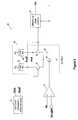
- FIG. 1is a schematic diagram of a prior art analog delay line.
- FIG. 2is a prior art compensating circuit that may be used with the analog delay line of FIG. 1 .
- FIG. 3is a schematic of an embodiment of a compensating circuit that may compensate for variations in the transconductance of input transistors in an analog delay line.
- FIG. 4is a schematic diagram of an embodiment of a differential-to-single converter that may be used in the compensating circuit shown in FIG. 3 .
- FIG. 5is a schematic diagram of an embodiment of an analog delay line.
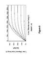
- FIG. 6is a chart illustrating the manner in which the analog delay line of FIG. 5 or an analog delay line according to some other embodiment may operate.
- the delay line 10includes a plurality of differential amplifiers 12 a,b . . . n that are coupled to each other in series between a first differential amplifier 12 a and a last differential amplifier 12 n .
- Each of the differential amplifiers 12 a,b . . . nmay be substantially identical to each other, so only one differential amplifier 12 a is shown in detail in FIG. 1 .
- Each differential amplifier 12includes first and second input transistors 16 , 18 , which may be nFET input transistors as shown in FIG. 1 .
- the respective sources of the input transistors 16 , 18may be coupled to each other and to a current sink 20 .
- the drainsmay be coupled to a supply voltage Vcc through respective load resistances 24 , 26 .
- the gates of the input transistors 16 , 18may be coupled to receive respective differential input signals In and InF that are to be delayed.
- the input signals In and InFare delayed as they propagate through each of the differential amplifiers 12 a . . . n to provide (e.g., generate) differential output signals Out, OutF at the drains of the respective input transistors 16 , 18 .
- the delay provided by the analog delay line 10may, in part, be determined by the number of differential amplifiers 12 in the delay line 10 .
- the combined resistances 24 , 26may be much smaller than the source-to-drain resistance of the transistors 16 , 18 so that R ⁇ Rt may essentially be equal to R.
- the transconductance gmis, in turn, a function of the current drawn through the input transistors 16 , 18 by the current sink 20 .
- the current sink 20may be implemented by a current sink transistor 30 , such as an nFET transistor.
- the gain G of each of the differential amplifiers 12is a function of the magnitude of the current drawn by the current sink transistor 30
- controlling the current drawn by the transistor 30may facilitate maintaining the gain of the differential amplifiers 12 substantially constant.
- prior art analog delay lines 10may use a compensating circuit 34 to adjust the magnitude of a Bias voltage applied to the gate of the current sink transistor 30 for the purpose of maintaining the current drawn by transistor 10 constant.
- the compensating circuit 40may include a transistor 44 , such as a nFET transistor as shown in FIG. 2 , which may be the same as the current sink transistor 30 and may be exposed to the same process, supply voltage and temperature as the transistor 30 .
- the transistor 44may have a source coupled to a first supply voltage, such as ground, and a drain coupled through a load 46 , such as a resistance, to a second supply voltage, such as Vcc.
- a gate of the transistor 44may be coupled to an output of a differential amplifier 48 that may have a first input coupled to receive a feedback voltage Vf from the drain of the transistor 44 and a second input coupled to receive a reference voltage Vr.
- the magnitude of the feedback voltage Vfcorresponds to the magnitude of the supply voltage Vcc less a voltage drop across the load 46 .
- the magnitude of the feedback voltage Vfmay be inversely proportional to the current drawn by the transistor 44 .
- the current drawn by the transistor 44may, in turn, be proportional to the transconductance gm of the transistor 44 and the voltage at the output of the differential amplifier 48 .
- the transconductance gm of the transistor 44increases, the current drawn by the transistor 44 will increase, thereby decreasing the magnitude of the feedback voltage Vf so that it is less than the magnitude of the reference voltage Vr.
- the voltage at the output of the differential amplifier 48will decrease, thereby reducing the voltage applied to the gate of the transistor 44 .
- the current drawn by the transistor 44will then decrease to increase the magnitude of the feedback voltage Vf. If the closed loop gain through the transistor 44 and differential amplifier 48 is sufficiently high, the voltage applied to the gate of the transistor 44 will be reduced to a level that causes the current through the load 46 to decrease sufficiently such that the feedback voltage is again substantially equal to the magnitude of the reference voltage Vr.
- the compensating circuit 40operates in a similar manner in response to a decrease in the transconductance gm of the transistor 44 .
- the magnitude of the current drawn by the transistor 44is maintained substantially constant, i.e., at the current that causes the feedback voltage Vf to be substantially equal to the reference voltage Vr.
- the compensating circuit 40may therefore ensure that the current drawn by the transistor 44 is substantially insensitive to changes in the transconductance gm of the transistor 44 resulting from various factors such as process variations in fabricating the transistor 44 , the supply voltage Vcc, and the temperature of the transistor 44 .
- the transconductance gm of the transistor 44may change in the same manner as the transconductance gm of a transistor used as the transistor 30 ( FIG. 1 ) of the differential amplifiers 12 in the analog delay line 10 .
- the analog delay line 10may be made substantially insensitive to changes in the transconductance gm of the transistors 30 used in the delay line by applying the output of the differential amplifier 48 to the gates of the transistors 30 .
- the gain of the differential amplifiers 12 used in the analog delay line 32may be maintained at a relatively constant value despite variations in the gm of the current sink transistors.
- the compensating circuit 40may be able to make the analog delay line 10 substantially insensitive to changes in the transconductance gm of the current sink transistors in the differential amplifiers 12 , it may not compensate for changes in the transconductance gm of the input transistors 16 , 18 used in the differential amplifiers 12 .
- an embodiment of a compensating circuit 50 shown in FIG. 3may compensate for changes in the transconductance gm of the input transistors 16 , 18 used in the differential amplifiers 12 ( FIG. 1 ).
- the compensating circuit 50may include a bias voltage generator 54 having first and second input transistors 56 , 58 , which may be nFET input transistors as shown in FIG. 3 .
- the input transistors 56 , 58may have substantially the same electrical characteristics, and may be formed using the same semiconductor material, as the input transistors 16 , 18 used in an analog delay line with which the compensating circuit 50 is used.
- the respective sources of the input transistors 56 , 58may be coupled to each other and to a current sink 60 , which may be a current sink transistor 62 , such as a nFET transistor.
- the current sink transistor 62may also have the same electrical characteristics, and may be formed using the same semiconductor material, as the current sink transistor 30 used in an analog delay line with which the compensating circuit 50 is used.
- the drains of the input transistors 56 , 58may be coupled to a supply voltage such as Vcc through respective loads 64 , 66 , which may be resistances.
- the gate of the input transistor 56may be coupled to the drain of the transistor 58 to provide a first output signal Aout, and the gate of the input transistor 58 may be similarly coupled to the drain of the transistor 56 to provide a second output signal A
- the output signals Aout and AoutFmay be applied to respective inputs of a differential-to-single converter 68 , which may provide a feedback voltage FB at its single output.
- the magnitude of the feedback voltage FBmay be equal to the magnitude of the differential output voltage of the bias voltage generator 54 , i.e., Aout ⁇ AoutF.
- the feedback voltage VBmay be applied to a first input of a comparison circuit, such as a differential amplifier 70 .
- a second input of the differential amplifier 70may receive a reference voltage SwingRef, which, as explained in greater detail below, may be indicative of the desired peak-to-peak voltage of a differential signal propagating through an analog delay line with which the compensating circuit 50 is used.
- a start circuit 74may be used to provide a differential output signal that is initially applied to the gates of the input transistors 56 , 58 for reasons that will be explained below.
- the gains of differential amplifiers used in an analog delay lineshould be unity so that the amplitude of a signal propagating through the delay line can be controlled with some degree of precision. If the gain is significantly greater than unity, a signal coupled though a delay line may progressively increase in magnitude until the signal transitions between Vcc and ground. Conversely, if the gain is significantly less than unity, a signal coupled though a delay line may progressively decrease in magnitude until it is no longer being propagated through the delay line.
- the voltage gain of the bias voltage generator 54is inherently unity since voltage gain is defined as the ratio of the output voltage to the input voltage, and the differential output voltage Vout ⁇ VoutF is equal to the differential input voltage Vout ⁇ VoutF.
- the differential output voltage Aout ⁇ AoutFcan be set by selecting an appropriate resistance of the loads 64 , 66 and gm of the transistors 56 , 58 , which can be adjusted by varying the current drawn by the current sink transistor 62 .
- the differential-to-single converter 68provides a feedback voltage FB that corresponds to the differential output voltage of the bias voltage generator 54 , i.e., Aout ⁇ AoutF.
- the differential amplifier 70then adjusts the current drawn by the current sink transistor 62 to adjust the gm of the input transistors 56 , 58 until the magnitude of the feedback voltage FB is substantially equal to the magnitude of the reference voltage SwingRef.
- the gain of the bias voltage generator 54may be automatically adjusted so that the gain is substantially unity at a specific differential output voltage.
- a start circuit 74may therefore be provided to initially provide (e.g., apply, supply, output, etc.) a differential voltage to the gates of the transistors 56 , 58 that ensures that the magnitude of Aout is greater than the magnitude of AoutF and of the correct polarity so that Aout is greater than AoutF.
- the magnitude of the voltageis not critical since the input/output voltages Aout, AoutF will automatically adjust to the correct values so that the gain of the bias voltage generator 54 is substantially unity.
- the converter 80includes a pair of differential input transistors 84 , 86 , which may be nFET transistors, having respective drains that are coupled to each other and to the drain of a current sink transistor 88 , which may also be a nFET transistor.
- the transistor 88has a source coupled to a first supply voltage, such as ground, and a gate coupled to receive the Bias voltage provided by the bias voltage generator 54 .
- the gate of each of the transistors 84 , 86is coupled to receive a respective signal Aout, AoutF from the bias voltage generator 54 .
- Each of the transistors 84 , 86is coupled in series with a respective transistor 90 , 92 , which may be pFET transistors.
- the sources of the transistorsmay be coupled to a second supply voltage, such as Vcc, and the respective gates of the transistors 90 , 92 may be coupled to each other and to the drain of the nFET transistor 84 .
- the drain of the transistor 92is coupled to the second supply voltage through a load 96 , and it provides the feedback voltage FB that is fed back to the input of the differential amplifier 70 ( FIG. 3 ).
- the transistors 84 , 86 , 88may have substantially the same electrical characteristics, and may be formed using the same semiconductor material (e.g., in the same substrate), as the transistors 56 , 58 , 62 , respectively, in the bias voltage generator 54 .
- the differential-to-single converter 80In operation, if the magnitude of the feedback voltage FB may be indicative of, and varies inversely with, the magnitude of the differential input voltage Vout ⁇ VoutF, the differential-to-single converter 80 thus provides a single voltage FB corresponding to the magnitude of the different output voltage Vout ⁇ FoutF of the bias voltage generator 54 .
- the compensating circuit 50 or a compensating circuitmay be used with an embodiment of an analog delay line 100 as shown in FIG. 5 .
- the analog delay line 100may use a plurality of delay stages 112 a , 112 b . . . 112 n , which may be the same as or different from the delay stages 12 a,b . . . 12 n used in the prior art delay line 10 of FIG. 1 .
- each of the delay stages 112 auses a differential amplifier having input transistors 116 , 118 , which may be nFET transistors, a pair of load resistances 124 , 126 and a current sink transistor 130 .
- the transistors 116 , 118 , 130may be the same as or different from the transistors 56 , 58 , 62 , respectively, used in the bias voltage generator 54 of FIG. 3 .
- the gate of the current sink transistor 130receives the bias voltage BIAS provided by a compensating circuit 134 , which, as mentioned above, may be the compensating circuit 50 or some other embodiment of a compensating circuit.
- the first delay stage 112 areceives a differential input voltage In, InF
- the last delay stage 112 nprovides a differential output voltage Out, OutF that is delayed in time relative to the differential input voltage In, InF.
- the manner in which the analog delay line 100 operatesmay be explained with reference to the chart shown in FIG. 6 .
- the magnitude of the differential input voltage In ⁇ InF applied to each of the stages 112 of the analog delay line 100is shown on the horizontal axis in opposite directions from the center (i.e., the voltage of In is plotted to the left of center and the voltage of InF is plotted to the right of center).
- the differential output voltage Out ⁇ OutF from each of the stages 112is shown on the vertical axis from bottom to top.
- Each of the curvesis indicative of the differential output voltage as a function of differential input voltage at a respective current drawn by the current sink transistor 130 .
- the gain of the stage 112i.e., the slope of the curve corresponding to a specific current drawn by the current sink transistor 130 , decreases with increases in the differential input voltage.
- smaller amplitude input signalsmay be amplified to a greater extent than larger amplitude input signals.
- the points where the magnitude of the differential input signals are equal to the magnitudes of the corresponding differential output signalsis where the gain of the delay stage 112 is unity. As shown in FIG. 6 , these points form straight lines.
- the portions of the gain curves below the straight linesrepresent a gain of less than unity, and the portions of the gain curves above the straight lines represent a gain of greater than unity.
- the differential input signalis amplified to provide a larger differential output signal.
- the differential input signalis attenuated to provide a smaller differential output signal.
- each of the delay stages 112may be set to cause the delay stage to have a substantially unity gain at a differential output voltage amplitude corresponding to the SwingRef ( FIG. 3 )
- a differential input signal propagating though the delay line 110will either be attenuated or amplified by each of the delay stages 112 in sequence until the amplitude of the output signal of the stage 112 is equal to the SwingRef voltage.
- the differential output signalmay then propagate though any remaining stages with a substantially constant amplitude, and may be output from the final delay stage 112 n with the magnitude of the differential output signal being substantially equal to the SwingRef voltage.
- the output voltagewill converge on a differential output voltage of 200 mv. If the amplitude of a differential signal applied to any stage 112 is less than 200 mv, the gain of the stages 112 in the delay line 100 will be greater than unity so that the signal will eventually be amplified to 200 mv. On the other hand, if the amplitude of a differential signal applied to any stage is greater than 200 mv, the gain of the stages 112 in the delay line 100 will be less than unity so that the signal will eventually be attenuated to 200 mv.
- the compensating circuit 150may automatically adjust the bias voltage Bias to control the current drawn by the current sink transistor 130 so that the gain of the delay stages 112 are again substantially unity at a differential output voltage corresponding to the SwingRef voltage.
Landscapes
- Engineering & Computer Science (AREA)
- Power Engineering (AREA)
- Amplifiers (AREA)
Abstract
Description
G=vin*gm*R∥Rt [Equation 1],
where Vin is the amplitude of the differential input signal, i.e., In−InF, gm is the transconductance of the
G=Vin*gm*R∥Rt [Equation 1],
where Vin is the amplitude of the differential input signal, i.e., Aout−AoutF, gm is the transconductance of the
Vout=1/[gm*R∥Rt] [Equation 2].
If the resistance of the
Vout=1/[gm*R] [Equation 3].
Thus, the differential output voltage Aout−AoutF can be set by selecting an appropriate resistance of the
Claims (9)
Priority Applications (3)
| Application Number | Priority Date | Filing Date | Title |
|---|---|---|---|
| US12/854,749US8283950B2 (en) | 2010-08-11 | 2010-08-11 | Delay lines, amplifier systems, transconductance compensating systems and methods of compensating |
| US13/605,729US8710871B2 (en) | 2010-08-11 | 2012-09-06 | Delay lines, amplifier systems, transconductance compensating systems and methods of compensating |
| US13/605,739US8779802B2 (en) | 2010-08-11 | 2012-09-06 | Delay lines, amplifier systems, transconductance compensating systems and methods of compensating |
Applications Claiming Priority (1)
| Application Number | Priority Date | Filing Date | Title |
|---|---|---|---|
| US12/854,749US8283950B2 (en) | 2010-08-11 | 2010-08-11 | Delay lines, amplifier systems, transconductance compensating systems and methods of compensating |
Related Child Applications (2)
| Application Number | Title | Priority Date | Filing Date |
|---|---|---|---|
| US13/605,729DivisionUS8710871B2 (en) | 2010-08-11 | 2012-09-06 | Delay lines, amplifier systems, transconductance compensating systems and methods of compensating |
| US13/605,739DivisionUS8779802B2 (en) | 2010-08-11 | 2012-09-06 | Delay lines, amplifier systems, transconductance compensating systems and methods of compensating |
Publications (2)
| Publication Number | Publication Date |
|---|---|
| US20120038405A1 US20120038405A1 (en) | 2012-02-16 |
| US8283950B2true US8283950B2 (en) | 2012-10-09 |
Family
ID=45564380
Family Applications (3)
| Application Number | Title | Priority Date | Filing Date |
|---|---|---|---|
| US12/854,749Active2030-09-20US8283950B2 (en) | 2010-08-11 | 2010-08-11 | Delay lines, amplifier systems, transconductance compensating systems and methods of compensating |
| US13/605,729ActiveUS8710871B2 (en) | 2010-08-11 | 2012-09-06 | Delay lines, amplifier systems, transconductance compensating systems and methods of compensating |
| US13/605,739ActiveUS8779802B2 (en) | 2010-08-11 | 2012-09-06 | Delay lines, amplifier systems, transconductance compensating systems and methods of compensating |
Family Applications After (2)
| Application Number | Title | Priority Date | Filing Date |
|---|---|---|---|
| US13/605,729ActiveUS8710871B2 (en) | 2010-08-11 | 2012-09-06 | Delay lines, amplifier systems, transconductance compensating systems and methods of compensating |
| US13/605,739ActiveUS8779802B2 (en) | 2010-08-11 | 2012-09-06 | Delay lines, amplifier systems, transconductance compensating systems and methods of compensating |
Country Status (1)
| Country | Link |
|---|---|
| US (3) | US8283950B2 (en) |
Cited By (5)
| Publication number | Priority date | Publication date | Assignee | Title |
|---|---|---|---|---|
| US20110235450A1 (en)* | 2010-03-26 | 2011-09-29 | Micron Technology, Inc. | Current mode sense amplifier with passive load |
| US20130009705A1 (en)* | 2010-01-26 | 2013-01-10 | Micron Technology, Inc. | Sense amplifier having loop gain control |
| US8472899B2 (en)* | 2007-02-26 | 2013-06-25 | Broadcom Corporation | Power control for linear and class AB power amplifiers |
| US8710871B2 (en) | 2010-08-11 | 2014-04-29 | Micron Technology, Inc. | Delay lines, amplifier systems, transconductance compensating systems and methods of compensating |
| US8810281B2 (en) | 2011-07-26 | 2014-08-19 | Micron Technology, Inc. | Sense amplifiers including bias circuits |
Families Citing this family (4)
| Publication number | Priority date | Publication date | Assignee | Title |
|---|---|---|---|---|
| US8716984B2 (en)* | 2009-06-29 | 2014-05-06 | Advanced Energy Industries, Inc. | Method and apparatus for modifying the sensitivity of an electrical generator to a nonlinear load |
| US9906235B2 (en)* | 2016-04-12 | 2018-02-27 | Microchip Technology Incorporated | Microcontroller with digital delay line analog-to-digital converters and digital comparators |
| KR20180045677A (en)* | 2016-10-26 | 2018-05-04 | 에스케이하이닉스 주식회사 | Receving device, transmitting device, semiconductor apparatus and system using the same |
| US10285087B2 (en)* | 2016-11-10 | 2019-05-07 | Honeywell International Inc. | Efficient event-triggered reporting system |
Citations (41)
| Publication number | Priority date | Publication date | Assignee | Title |
|---|---|---|---|---|
| US4284957A (en) | 1979-09-28 | 1981-08-18 | American Microsystems, Inc. | CMOS Operational amplifier with reduced power dissipation |
| US4502020A (en) | 1983-10-26 | 1985-02-26 | Comlinear Corporation | Settling time reduction in wide-band direct-coupled transistor amplifiers |
| US4555673A (en) | 1984-04-19 | 1985-11-26 | Signetics Corporation | Differential amplifier with rail-to-rail input capability and controlled transconductance |
| US4586166A (en) | 1983-08-31 | 1986-04-29 | Texas Instruments Incorporated | SRAM with improved sensing circuit |
| US4843343A (en) | 1988-01-04 | 1989-06-27 | Motorola, Inc. | Enhanced Q current mode active filter |
| US5473567A (en) | 1993-03-31 | 1995-12-05 | Sgs-Thomson Microelectronics, Inc. | Disabling sense amplifier |
| US5477497A (en) | 1993-07-12 | 1995-12-19 | Samsung Electronics Co., Ltd. | Semiconductor memory device |
| US5493533A (en)* | 1994-09-28 | 1996-02-20 | Atmel Corporation | Dual differential trans-impedance sense amplifier and method |
| US5504442A (en) | 1992-12-28 | 1996-04-02 | Oki Electric Industry Co., Ltd. | Sense circuit |
| US5654928A (en) | 1995-04-28 | 1997-08-05 | Samsung Electronics Co. Ltd. | Current sense amplifier for use in a semiconductor memory device |
| US5710739A (en) | 1994-08-31 | 1998-01-20 | Sgs-Thomson Microelectronics, S.R.L. | Reading circuit for memory cells |
| US6127853A (en) | 1998-12-31 | 2000-10-03 | Taiwan Semiconductor Manufacturing Co., Ltd. | High speed current-mode sense-amplifier |
| US6141246A (en) | 1998-04-01 | 2000-10-31 | National Semiconductor Corporation | Memory device with sense amplifier that sets the voltage drop across the cells of the device |
| US6191989B1 (en)* | 2000-03-07 | 2001-02-20 | International Business Machines Corporation | Current sensing amplifier |
| US6326815B1 (en) | 1999-07-10 | 2001-12-04 | Samsung Electronics Co., Ltd. | Sense amplifier of semiconductor integrated circuit |
| US6396310B2 (en) | 2000-07-18 | 2002-05-28 | Samsung Electronics Co., Ltd. | Current sense amplifiers enabling amplification of bit line voltages provided by bit line sense amplifiers |
| US6483353B2 (en) | 2000-10-31 | 2002-11-19 | Samsung Electronics Co., Ltd. | Current sense amplifier circuits containing latches for improving stability and amplification in semiconductor devices |
| US6483351B2 (en) | 2001-02-26 | 2002-11-19 | Samsung Electronics Co., Ltd. | Input-output line sense amplifier having small current consumption and direct current |
| US6617885B2 (en) | 2000-08-09 | 2003-09-09 | Samsung Electronics Co., Ltd. | Sense amplifiers having gain control circuits therein that inhibit signal oscillations |
| US6721218B2 (en) | 2001-02-23 | 2004-04-13 | Samsung Electronics Co., Ltd. | Semiconductor memory device and data read method thereof |
| US6738302B1 (en) | 2003-02-07 | 2004-05-18 | United Memories, Inc. | Optimized read data amplifier and method for operating the same in conjunction with integrated circuit devices incorporating memory arrays |
| US6879217B2 (en) | 2003-09-05 | 2005-04-12 | Gennum Corporation | Triode region MOSFET current source to bias a transimpedance amplifier |
| US6879533B2 (en) | 2002-09-17 | 2005-04-12 | Samsung Electronics Co., Ltd. | Integrated circuit memory devices including active load circuits and related methods |
| US6894564B1 (en) | 2003-07-07 | 2005-05-17 | Analog Devices, Inc. | Variable-gain amplifier having error amplifier with constant loop gain |
| US6944066B1 (en) | 2004-04-29 | 2005-09-13 | Micron Technology, Inc. | Low voltage data path and current sense amplifier |
| US7038963B2 (en) | 2004-03-03 | 2006-05-02 | Samsung Electronics Co., Ltd. | Current sense amplifier circuits having a bias voltage node for adjusting input resistance |
| US7075368B2 (en) | 2003-09-01 | 2006-07-11 | Realtek Semiconductor Corp. | Linear-in-decibel variable gain amplifier |
| US7154331B2 (en) | 2004-06-29 | 2006-12-26 | Intel Corporation | Adapting operational amplifier frequency response respective to closed loop gain |
| US7262638B2 (en) | 2002-03-19 | 2007-08-28 | Samsung Electronics Co., Ltd. | Current sense amplifier |
| US7286011B2 (en) | 2005-06-07 | 2007-10-23 | Himax Technologies Limited | Operational amplifier circuit having adjustable bias current |
| US7342451B2 (en) | 2005-08-05 | 2008-03-11 | Siemens Medical Soluitions Usa, Inc. | System for logarithmically controlling multiple variable gain amplifiers |
| US7446609B2 (en) | 2006-05-11 | 2008-11-04 | Via Technologies, Inc. | Variable gain amplifier with gain adjusting circuit |
| US7477076B2 (en) | 2006-12-04 | 2009-01-13 | International Business Machines Corporation | Low-voltage, low-power-consumption, and high-speed differential current-sense amplification |
| US7521992B1 (en) | 2008-07-29 | 2009-04-21 | International Business Machines Corporation | Current-integrating amplifier |
| US7564295B2 (en) | 2007-06-27 | 2009-07-21 | Taiwan Semiconductor Manufacturing Co., Ltd. | Automatic bias circuit for sense amplifier |
| US7629817B2 (en) | 2007-02-09 | 2009-12-08 | Fujitsu Limited | System and apparatus for aperture time improvement |
| US7777568B2 (en) | 2004-12-02 | 2010-08-17 | Mandate Chips and Circuits Pvt. Ltd. | High frequency receiver preamplifier with CMOS rail-to-rail capability |
| US20110182129A1 (en) | 2010-01-26 | 2011-07-28 | Micron Technology, Inc. | Sense amplifier having loop gain control |
| US7990792B2 (en) | 2008-05-06 | 2011-08-02 | Micron Technology, Inc. | Hybrid sense amplifier and method, and memory device using same |
| US20110235450A1 (en) | 2010-03-26 | 2011-09-29 | Micron Technology, Inc. | Current mode sense amplifier with passive load |
| US8049535B2 (en) | 2004-05-04 | 2011-11-01 | Silicon Storage Technology, Inc. | Sense amplifier for low voltage high speed sensing |
Family Cites Families (24)
| Publication number | Priority date | Publication date | Assignee | Title |
|---|---|---|---|---|
| US4792923A (en) | 1985-08-30 | 1988-12-20 | Mitsubishi Denki Kabushiki Kaisha | Bipolar semiconductor memory device with double word lines structure |
| US4837523A (en) | 1988-04-04 | 1989-06-06 | Elantec | High slew rate linear amplifier |
| US6271977B1 (en) | 1999-02-16 | 2001-08-07 | International Business Machines Corporation | Multi-state preamplifier for disk drives |
| US6456161B2 (en) | 2000-06-13 | 2002-09-24 | Fairchild Semiconductor Corporation | Enhanced slew rate in amplifier circuits |
| US20030179842A1 (en)* | 2002-03-22 | 2003-09-25 | Kane Michael G. | Digital pattern sequence generator |
| CA2425647C (en) | 2002-04-16 | 2006-06-13 | Research In Motion Limited | System and method of amplifier gain control by variable bias and degeneration |
| US6798250B1 (en) | 2002-09-04 | 2004-09-28 | Pixim, Inc. | Current sense amplifier circuit |
| US6750714B1 (en) | 2002-12-16 | 2004-06-15 | Xerox Corporation | Opamp with infinite open loop gain |
| JP2006018663A (en) | 2004-07-02 | 2006-01-19 | Fujitsu Ltd | Current stabilization circuit, current stabilization method, and solid-state imaging device |
| US7154923B2 (en) | 2004-08-24 | 2006-12-26 | International Business Machines Corporation | Method and apparatus for providing a modulation current |
| US7315270B2 (en) | 2005-03-04 | 2008-01-01 | The Regents Of The University Of Colorado | Differential delay-line analog-to-digital converter |
| GB2424773A (en) | 2005-03-31 | 2006-10-04 | Seiko Epson Corp | A sense amplifier with a common-gate input stage |
| US7956641B1 (en) | 2005-04-28 | 2011-06-07 | Cypress Semiconductor Corporation | Low voltage interface circuit |
| US7265620B2 (en) | 2005-07-06 | 2007-09-04 | Pericom Semiconductor Corp. | Wide-band high-gain limiting amplifier with parallel resistor-transistor source loads |
| US7368991B2 (en) | 2006-01-05 | 2008-05-06 | Texas Instruments Incorporated | System and method for clamping a differential amplifier |
| US7616941B2 (en) | 2007-02-26 | 2009-11-10 | Broadcom Corporation | Method and system for improving efficiency over power control for linear and class AB power amplifiers |
| US7813199B2 (en) | 2008-04-22 | 2010-10-12 | Micron Technology, Inc. | Current mode data sensing and propagation using voltage amplifier |
| US8219343B2 (en)* | 2008-04-24 | 2012-07-10 | Realtek Semiconductor Corp. | Method and apparatus for calibrating a delay chain |
| TWI380153B (en) | 2009-01-15 | 2012-12-21 | Nanya Technology Corp | Signal receiver and voltage compensation method thereof |
| US7889006B1 (en) | 2009-09-23 | 2011-02-15 | Maxim Integrated Products, Inc. | dB-linear process-independent variable gain amplifier |
| US8344806B1 (en) | 2009-09-29 | 2013-01-01 | Amalfi Semiconductor, Inc. | Power amplifier with power feedback |
| US8030972B2 (en) | 2009-11-17 | 2011-10-04 | Zoran Corporation | High-speed latched comparator circuit with variable positive feedback |
| US8283950B2 (en) | 2010-08-11 | 2012-10-09 | Micron Technology, Inc. | Delay lines, amplifier systems, transconductance compensating systems and methods of compensating |
| US8810281B2 (en) | 2011-07-26 | 2014-08-19 | Micron Technology, Inc. | Sense amplifiers including bias circuits |
- 2010
- 2010-08-11USUS12/854,749patent/US8283950B2/enactiveActive
- 2012
- 2012-09-06USUS13/605,729patent/US8710871B2/enactiveActive
- 2012-09-06USUS13/605,739patent/US8779802B2/enactiveActive
Patent Citations (42)
| Publication number | Priority date | Publication date | Assignee | Title |
|---|---|---|---|---|
| US4284957A (en) | 1979-09-28 | 1981-08-18 | American Microsystems, Inc. | CMOS Operational amplifier with reduced power dissipation |
| US4586166A (en) | 1983-08-31 | 1986-04-29 | Texas Instruments Incorporated | SRAM with improved sensing circuit |
| US4502020A (en) | 1983-10-26 | 1985-02-26 | Comlinear Corporation | Settling time reduction in wide-band direct-coupled transistor amplifiers |
| US4555673A (en) | 1984-04-19 | 1985-11-26 | Signetics Corporation | Differential amplifier with rail-to-rail input capability and controlled transconductance |
| US4843343A (en) | 1988-01-04 | 1989-06-27 | Motorola, Inc. | Enhanced Q current mode active filter |
| US5504442A (en) | 1992-12-28 | 1996-04-02 | Oki Electric Industry Co., Ltd. | Sense circuit |
| US5514986A (en) | 1992-12-28 | 1996-05-07 | Oki Electric Industry Co., Ltd. | Sense circuit, memory circuit, negative-resistance circuit, schmitt trigger, load circuit, level shifter, and amplifier |
| US5473567A (en) | 1993-03-31 | 1995-12-05 | Sgs-Thomson Microelectronics, Inc. | Disabling sense amplifier |
| US5477497A (en) | 1993-07-12 | 1995-12-19 | Samsung Electronics Co., Ltd. | Semiconductor memory device |
| US5710739A (en) | 1994-08-31 | 1998-01-20 | Sgs-Thomson Microelectronics, S.R.L. | Reading circuit for memory cells |
| US5493533A (en)* | 1994-09-28 | 1996-02-20 | Atmel Corporation | Dual differential trans-impedance sense amplifier and method |
| US5654928A (en) | 1995-04-28 | 1997-08-05 | Samsung Electronics Co. Ltd. | Current sense amplifier for use in a semiconductor memory device |
| US6141246A (en) | 1998-04-01 | 2000-10-31 | National Semiconductor Corporation | Memory device with sense amplifier that sets the voltage drop across the cells of the device |
| US6127853A (en) | 1998-12-31 | 2000-10-03 | Taiwan Semiconductor Manufacturing Co., Ltd. | High speed current-mode sense-amplifier |
| US6326815B1 (en) | 1999-07-10 | 2001-12-04 | Samsung Electronics Co., Ltd. | Sense amplifier of semiconductor integrated circuit |
| US6191989B1 (en)* | 2000-03-07 | 2001-02-20 | International Business Machines Corporation | Current sensing amplifier |
| US6396310B2 (en) | 2000-07-18 | 2002-05-28 | Samsung Electronics Co., Ltd. | Current sense amplifiers enabling amplification of bit line voltages provided by bit line sense amplifiers |
| US6617885B2 (en) | 2000-08-09 | 2003-09-09 | Samsung Electronics Co., Ltd. | Sense amplifiers having gain control circuits therein that inhibit signal oscillations |
| US6483353B2 (en) | 2000-10-31 | 2002-11-19 | Samsung Electronics Co., Ltd. | Current sense amplifier circuits containing latches for improving stability and amplification in semiconductor devices |
| US6721218B2 (en) | 2001-02-23 | 2004-04-13 | Samsung Electronics Co., Ltd. | Semiconductor memory device and data read method thereof |
| US6483351B2 (en) | 2001-02-26 | 2002-11-19 | Samsung Electronics Co., Ltd. | Input-output line sense amplifier having small current consumption and direct current |
| US7262638B2 (en) | 2002-03-19 | 2007-08-28 | Samsung Electronics Co., Ltd. | Current sense amplifier |
| US6879533B2 (en) | 2002-09-17 | 2005-04-12 | Samsung Electronics Co., Ltd. | Integrated circuit memory devices including active load circuits and related methods |
| US6738302B1 (en) | 2003-02-07 | 2004-05-18 | United Memories, Inc. | Optimized read data amplifier and method for operating the same in conjunction with integrated circuit devices incorporating memory arrays |
| US6894564B1 (en) | 2003-07-07 | 2005-05-17 | Analog Devices, Inc. | Variable-gain amplifier having error amplifier with constant loop gain |
| US7075368B2 (en) | 2003-09-01 | 2006-07-11 | Realtek Semiconductor Corp. | Linear-in-decibel variable gain amplifier |
| US6879217B2 (en) | 2003-09-05 | 2005-04-12 | Gennum Corporation | Triode region MOSFET current source to bias a transimpedance amplifier |
| US7038963B2 (en) | 2004-03-03 | 2006-05-02 | Samsung Electronics Co., Ltd. | Current sense amplifier circuits having a bias voltage node for adjusting input resistance |
| US6944066B1 (en) | 2004-04-29 | 2005-09-13 | Micron Technology, Inc. | Low voltage data path and current sense amplifier |
| US8049535B2 (en) | 2004-05-04 | 2011-11-01 | Silicon Storage Technology, Inc. | Sense amplifier for low voltage high speed sensing |
| US7154331B2 (en) | 2004-06-29 | 2006-12-26 | Intel Corporation | Adapting operational amplifier frequency response respective to closed loop gain |
| US7777568B2 (en) | 2004-12-02 | 2010-08-17 | Mandate Chips and Circuits Pvt. Ltd. | High frequency receiver preamplifier with CMOS rail-to-rail capability |
| US7286011B2 (en) | 2005-06-07 | 2007-10-23 | Himax Technologies Limited | Operational amplifier circuit having adjustable bias current |
| US7342451B2 (en) | 2005-08-05 | 2008-03-11 | Siemens Medical Soluitions Usa, Inc. | System for logarithmically controlling multiple variable gain amplifiers |
| US7446609B2 (en) | 2006-05-11 | 2008-11-04 | Via Technologies, Inc. | Variable gain amplifier with gain adjusting circuit |
| US7477076B2 (en) | 2006-12-04 | 2009-01-13 | International Business Machines Corporation | Low-voltage, low-power-consumption, and high-speed differential current-sense amplification |
| US7629817B2 (en) | 2007-02-09 | 2009-12-08 | Fujitsu Limited | System and apparatus for aperture time improvement |
| US7564295B2 (en) | 2007-06-27 | 2009-07-21 | Taiwan Semiconductor Manufacturing Co., Ltd. | Automatic bias circuit for sense amplifier |
| US7990792B2 (en) | 2008-05-06 | 2011-08-02 | Micron Technology, Inc. | Hybrid sense amplifier and method, and memory device using same |
| US7521992B1 (en) | 2008-07-29 | 2009-04-21 | International Business Machines Corporation | Current-integrating amplifier |
| US20110182129A1 (en) | 2010-01-26 | 2011-07-28 | Micron Technology, Inc. | Sense amplifier having loop gain control |
| US20110235450A1 (en) | 2010-03-26 | 2011-09-29 | Micron Technology, Inc. | Current mode sense amplifier with passive load |
Cited By (14)
| Publication number | Priority date | Publication date | Assignee | Title |
|---|---|---|---|---|
| US8774740B2 (en) | 2007-02-26 | 2014-07-08 | Broadcom Corporation | Power control for power amplifiers |
| US8472899B2 (en)* | 2007-02-26 | 2013-06-25 | Broadcom Corporation | Power control for linear and class AB power amplifiers |
| US8472898B2 (en)* | 2007-02-26 | 2013-06-25 | Broadcom Corporation | Power amplifiers with improved efficiency over power control |
| US20130278340A1 (en)* | 2007-02-26 | 2013-10-24 | Broadcom Corporation | Power Amplifiers with Improved Power Control |
| US8880011B2 (en)* | 2007-02-26 | 2014-11-04 | Broadcom Corporation | Power amplifiers with improved power control |
| US20130009705A1 (en)* | 2010-01-26 | 2013-01-10 | Micron Technology, Inc. | Sense amplifier having loop gain control |
| US8659965B2 (en)* | 2010-01-26 | 2014-02-25 | Micron Technology, Inc. | Sense amplifier having loop gain control |
| US9013942B2 (en) | 2010-01-26 | 2015-04-21 | Micron Technology, Inc. | Sense amplifier having loop gain control |
| US8705304B2 (en) | 2010-03-26 | 2014-04-22 | Micron Technology, Inc. | Current mode sense amplifier with passive load |
| US20110235450A1 (en)* | 2010-03-26 | 2011-09-29 | Micron Technology, Inc. | Current mode sense amplifier with passive load |
| US9484074B2 (en) | 2010-03-26 | 2016-11-01 | Micron Technology, Inc. | Current mode sense amplifier with load circuit for performance stability |
| US8779802B2 (en) | 2010-08-11 | 2014-07-15 | Micron Technology, Inc. | Delay lines, amplifier systems, transconductance compensating systems and methods of compensating |
| US8710871B2 (en) | 2010-08-11 | 2014-04-29 | Micron Technology, Inc. | Delay lines, amplifier systems, transconductance compensating systems and methods of compensating |
| US8810281B2 (en) | 2011-07-26 | 2014-08-19 | Micron Technology, Inc. | Sense amplifiers including bias circuits |
Also Published As
| Publication number | Publication date |
|---|---|
| US20130015899A1 (en) | 2013-01-17 |
| US20120038405A1 (en) | 2012-02-16 |
| US8779802B2 (en) | 2014-07-15 |
| US20120326786A1 (en) | 2012-12-27 |
| US8710871B2 (en) | 2014-04-29 |
Similar Documents
| Publication | Publication Date | Title |
|---|---|---|
| US8710871B2 (en) | Delay lines, amplifier systems, transconductance compensating systems and methods of compensating | |
| US8854023B2 (en) | Low dropout linear regulator | |
| US20100156539A1 (en) | Power amplifier system with power control function | |
| US9836070B2 (en) | Regulator with low dropout voltage and improved stability | |
| US4933644A (en) | Common-mode feedback bias generator for operational amplifiers | |
| US9146570B2 (en) | Load current compesating output buffer feedback, pass, and sense circuits | |
| US9209822B2 (en) | A/D converter and semiconductor integrated circuit | |
| US20150130647A1 (en) | Current amplifier circuit, integrator, and ad converter | |
| US7443240B2 (en) | AM intermediate frequency variable gain amplifier circuit, variable gain amplifier circuit and its semiconductor integrated circuit | |
| TW201633704A (en) | Differential amplifiers | |
| EP1435693B1 (en) | Amplification circuit | |
| CN114006610A (en) | Stabilizing circuit of frequency compensation circuit with self-adaptive load change | |
| US6339355B1 (en) | Offsetting comparator device and comparator circuit | |
| US6781462B2 (en) | Power amplifier | |
| KR100813464B1 (en) | Low Power Variable Gain Amplifier | |
| JP2007295566A (en) | Operational amplifier | |
| TW202005264A (en) | Amplifier circuitry, voltage regulator circuit, and signal compensantion method | |
| US20140266441A1 (en) | Three stage amplifier | |
| US7394318B2 (en) | Amplifier control system | |
| CN110531825B (en) | Amplifier circuit system, voltage regulation circuit and signal compensation method | |
| US20080315951A1 (en) | Class ab differential amplifier with output stage common mode feedback | |
| JP2015070552A (en) | Differential amplification circuit control device | |
| Ghosh et al. | Simplified design method for fully differential gain-boosted folded cascade OTA | |
| JP2005080090A (en) | Output voltage control circuit of differential amplifier circuit and voltage detector | |
| WO2021124450A1 (en) | Differential amplification circuit, reception circuit and semiconductor integrated circuit |
Legal Events
| Date | Code | Title | Description |
|---|---|---|---|
| AS | Assignment | Owner name:MICRON TECHNOLOGY, INC., IDAHO Free format text:ASSIGNMENT OF ASSIGNORS INTEREST;ASSIGNOR:WILLEY, AARON;REEL/FRAME:024825/0718 Effective date:20100723 | |
| FEPP | Fee payment procedure | Free format text:PAYOR NUMBER ASSIGNED (ORIGINAL EVENT CODE: ASPN); ENTITY STATUS OF PATENT OWNER: LARGE ENTITY | |
| STCF | Information on status: patent grant | Free format text:PATENTED CASE | |
| CC | Certificate of correction | ||
| FPAY | Fee payment | Year of fee payment:4 | |
| AS | Assignment | Owner name:U.S. BANK NATIONAL ASSOCIATION, AS COLLATERAL AGENT, CALIFORNIA Free format text:SECURITY INTEREST;ASSIGNOR:MICRON TECHNOLOGY, INC.;REEL/FRAME:038669/0001 Effective date:20160426 Owner name:U.S. BANK NATIONAL ASSOCIATION, AS COLLATERAL AGEN Free format text:SECURITY INTEREST;ASSIGNOR:MICRON TECHNOLOGY, INC.;REEL/FRAME:038669/0001 Effective date:20160426 | |
| AS | Assignment | Owner name:MORGAN STANLEY SENIOR FUNDING, INC., AS COLLATERAL AGENT, MARYLAND Free format text:PATENT SECURITY AGREEMENT;ASSIGNOR:MICRON TECHNOLOGY, INC.;REEL/FRAME:038954/0001 Effective date:20160426 Owner name:MORGAN STANLEY SENIOR FUNDING, INC., AS COLLATERAL Free format text:PATENT SECURITY AGREEMENT;ASSIGNOR:MICRON TECHNOLOGY, INC.;REEL/FRAME:038954/0001 Effective date:20160426 | |
| AS | Assignment | Owner name:U.S. BANK NATIONAL ASSOCIATION, AS COLLATERAL AGENT, CALIFORNIA Free format text:CORRECTIVE ASSIGNMENT TO CORRECT THE REPLACE ERRONEOUSLY FILED PATENT #7358718 WITH THE CORRECT PATENT #7358178 PREVIOUSLY RECORDED ON REEL 038669 FRAME 0001. ASSIGNOR(S) HEREBY CONFIRMS THE SECURITY INTEREST;ASSIGNOR:MICRON TECHNOLOGY, INC.;REEL/FRAME:043079/0001 Effective date:20160426 Owner name:U.S. BANK NATIONAL ASSOCIATION, AS COLLATERAL AGEN Free format text:CORRECTIVE ASSIGNMENT TO CORRECT THE REPLACE ERRONEOUSLY FILED PATENT #7358718 WITH THE CORRECT PATENT #7358178 PREVIOUSLY RECORDED ON REEL 038669 FRAME 0001. ASSIGNOR(S) HEREBY CONFIRMS THE SECURITY INTEREST;ASSIGNOR:MICRON TECHNOLOGY, INC.;REEL/FRAME:043079/0001 Effective date:20160426 | |
| AS | Assignment | Owner name:JPMORGAN CHASE BANK, N.A., AS COLLATERAL AGENT, ILLINOIS Free format text:SECURITY INTEREST;ASSIGNORS:MICRON TECHNOLOGY, INC.;MICRON SEMICONDUCTOR PRODUCTS, INC.;REEL/FRAME:047540/0001 Effective date:20180703 Owner name:JPMORGAN CHASE BANK, N.A., AS COLLATERAL AGENT, IL Free format text:SECURITY INTEREST;ASSIGNORS:MICRON TECHNOLOGY, INC.;MICRON SEMICONDUCTOR PRODUCTS, INC.;REEL/FRAME:047540/0001 Effective date:20180703 | |
| AS | Assignment | Owner name:MICRON TECHNOLOGY, INC., IDAHO Free format text:RELEASE BY SECURED PARTY;ASSIGNOR:U.S. BANK NATIONAL ASSOCIATION, AS COLLATERAL AGENT;REEL/FRAME:047243/0001 Effective date:20180629 | |
| AS | Assignment | Owner name:MICRON TECHNOLOGY, INC., IDAHO Free format text:RELEASE BY SECURED PARTY;ASSIGNOR:MORGAN STANLEY SENIOR FUNDING, INC., AS COLLATERAL AGENT;REEL/FRAME:050937/0001 Effective date:20190731 | |
| AS | Assignment | Owner name:MICRON SEMICONDUCTOR PRODUCTS, INC., IDAHO Free format text:RELEASE BY SECURED PARTY;ASSIGNOR:JPMORGAN CHASE BANK, N.A., AS COLLATERAL AGENT;REEL/FRAME:051028/0001 Effective date:20190731 Owner name:MICRON TECHNOLOGY, INC., IDAHO Free format text:RELEASE BY SECURED PARTY;ASSIGNOR:JPMORGAN CHASE BANK, N.A., AS COLLATERAL AGENT;REEL/FRAME:051028/0001 Effective date:20190731 | |
| MAFP | Maintenance fee payment | Free format text:PAYMENT OF MAINTENANCE FEE, 8TH YEAR, LARGE ENTITY (ORIGINAL EVENT CODE: M1552); ENTITY STATUS OF PATENT OWNER: LARGE ENTITY Year of fee payment:8 | |
| MAFP | Maintenance fee payment | Free format text:PAYMENT OF MAINTENANCE FEE, 12TH YEAR, LARGE ENTITY (ORIGINAL EVENT CODE: M1553); ENTITY STATUS OF PATENT OWNER: LARGE ENTITY Year of fee payment:12 |