US8283935B2 - Method of forming touch sensing circuit pattern - Google Patents
Method of forming touch sensing circuit patternDownload PDFInfo
- Publication number
- US8283935B2 US8283935B2US12/168,896US16889608AUS8283935B2US 8283935 B2US8283935 B2US 8283935B2US 16889608 AUS16889608 AUS 16889608AUS 8283935 B2US8283935 B2US 8283935B2
- Authority
- US
- United States
- Prior art keywords
- axial
- electrodes
- conductive lines
- forming
- lines
- Prior art date
- Legal status (The legal status is an assumption and is not a legal conclusion. Google has not performed a legal analysis and makes no representation as to the accuracy of the status listed.)
- Active, expires
Links
Images

Classifications
- G—PHYSICS
- G06—COMPUTING OR CALCULATING; COUNTING
- G06F—ELECTRIC DIGITAL DATA PROCESSING
- G06F3/00—Input arrangements for transferring data to be processed into a form capable of being handled by the computer; Output arrangements for transferring data from processing unit to output unit, e.g. interface arrangements
- G06F3/01—Input arrangements or combined input and output arrangements for interaction between user and computer
- G06F3/03—Arrangements for converting the position or the displacement of a member into a coded form
- G06F3/041—Digitisers, e.g. for touch screens or touch pads, characterised by the transducing means
- G06F3/044—Digitisers, e.g. for touch screens or touch pads, characterised by the transducing means by capacitive means
- G06F3/0446—Digitisers, e.g. for touch screens or touch pads, characterised by the transducing means by capacitive means using a grid-like structure of electrodes in at least two directions, e.g. using row and column electrodes
- G—PHYSICS
- G06—COMPUTING OR CALCULATING; COUNTING
- G06F—ELECTRIC DIGITAL DATA PROCESSING
- G06F3/00—Input arrangements for transferring data to be processed into a form capable of being handled by the computer; Output arrangements for transferring data from processing unit to output unit, e.g. interface arrangements
- G06F3/01—Input arrangements or combined input and output arrangements for interaction between user and computer
- G06F3/03—Arrangements for converting the position or the displacement of a member into a coded form
- G06F3/041—Digitisers, e.g. for touch screens or touch pads, characterised by the transducing means
- G06F3/044—Digitisers, e.g. for touch screens or touch pads, characterised by the transducing means by capacitive means
- G06F3/0443—Digitisers, e.g. for touch screens or touch pads, characterised by the transducing means by capacitive means using a single layer of sensing electrodes
- G—PHYSICS
- G06—COMPUTING OR CALCULATING; COUNTING
- G06F—ELECTRIC DIGITAL DATA PROCESSING
- G06F2203/00—Indexing scheme relating to G06F3/00 - G06F3/048
- G06F2203/041—Indexing scheme relating to G06F3/041 - G06F3/045
- G06F2203/04111—Cross over in capacitive digitiser, i.e. details of structures for connecting electrodes of the sensing pattern where the connections cross each other, e.g. bridge structures comprising an insulating layer, or vias through substrate
Definitions
- the inventionrelates to a method of forming a touch sensing circuit pattern, especially to a technology of forming a touch sensing circuit pattern on a glass substrate.
- Touch panelshave been widely used in home appliances, communication devices and electronic information products such as a personal digital assistant (PDA), a home appliance and a game input interface.
- PDApersonal digital assistant
- a touch panelis preferably integrated with a display panel, so a user can touch a displayed image to select an operation. Therefore, a touch panel makes more convenient for operating a PDA, a home appliance, a game input interface, and a public inquiry system.
- a touch sensing area of a conventional touch panelis normally arranged on a surface of a substrate.
- the touch sensing areais utilized for sensing a touch signal generated by a finger or a pen.
- the touch sensing areais made up of a transparent conductive film (such as ITO).
- ITOtransparent conductive film
- the conventional touch panelscan be divided into many types with reference to different technology principles, such as resistive touch panel, capacitive touch panel, infrared sensing touch panel, electromagnetic sensing touch panel and sound sensing touch panel.
- the capacitive touch paneldetects a capacitance change generated between a human body and a transparent electrode to determine the touch position.
- capacitive touch panelshave been widely used.
- U.S. Pat. No. 6,970,160disclosed a lattice touch-sensing system for detecting a position of a touch on a touch-sensitive surface.
- the lattice touch-sensing systemmay include two capacitive sensing layers, separated by an insulating material, and each layer consists of substantially parallel conducting elements. Each element may comprise a series of diamond shaped patch that are connected together with narrow conductive rectangular strips. Each conducting element of a given sensing layer is electrically connected to a conductive line.
- a control circuitmay also be included to provide an excitation signal to both sets of conducting elements through the corresponding conductive lines, to receive sensing signals generated by sensor elements when a touch on the surface occurs, and to determine the touch position on each layer.
- the inventionis to provide method of forming a touch sensing circuit pattern which forms two axial electrodes by sputtering, exposing, developing and etching at one time to simplify the manufacturing process.
- a method of forming a touch sensing circuit patternincludes steps of:
- first axial electrodesare arranged on two sides of a corresponding insulation barrier along a first direction so as to be connected by a corresponding first axial conductive line;
- two second axial electrodesare arranged on two sides of the first axial conductive line along the second direction;
- the second axial conductive linesare across on the insulation barriers and connect to the second axial electrodes to form a touch sensing circuit pattern.
- the first axial electrodes and the second axial electrodescan be formed on the transparent substrate by sputtering, exposing, developing and etching at one same time.
- the process of manufacturing the touch sensing circuit patternis simplified.
- the first axial conductive linesare made of transparent material or non-transparent material.
- first axial electrodes, the second axial conductive lines and the second axial electrodesare made of transparent material.
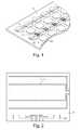
- FIG. 1is a perspective view of a touch sensing circuit pattern according to the invention.
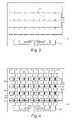
- FIG. 2 to FIG. 4are schematic views showing the steps of forming the touch sensing circuit pattern according to a preferred embodiment of the invention.
- FIG. 1is a perspective view of a touch sensing circuit pattern according to a preferred embodiment of the invention. A method of forming the touch sensing circuit is described in the following description.
- first axial conductive lines 11 parallel with each other and a plurality of second directional metal lines 23are formed on a transparent substrate 4 .
- the first axial conductive lines 11 and the second directional metal lines 23are made of a non-transparent conductive material such as aurum, silver, copper, aluminum or other metal material.
- the non-transparent conductive materialis coated on the transparent substrate 4 by sputtering or other equivalent process and then forms the first axial conductive lines 11 and the second directional metal lines 23 by exposing, developing and etching.
- a plurality of insulation barriers 3are formed on each of the first axial conductive lines 11 .
- the insulation barriers 3are made of an insulation material such as silicon dioxide or other equivalent insulation material.
- the insulation materialis coated on the first axial conductive lines 11 by sputtering and then to form the insulation barriers 3 by exposing, developing and etching.
- a plurality of separated first axial electrodes 12 and a plurality of separated second axial electrodes 22 and a plurality of parallel second axial conductive lines 21are formed on the transparent substrate 4 , according to the positions of the first axial conductive lines 11 , the second directional metal lines 23 and the insulation barriers 3 .
- Every two adjacent first axial electrodes 12are arranged on two sides of a corresponding insulation barrier 3 along the first direction so as to be connected by a corresponding first axial conductive line 11 .
- Every two adjacent second axial electrodes 22are arranged on two sides of the first axial conductive line 11 along the second direction.
- the second axial conductive lines 21are across on the insulation barriers 3 and connect to the second axial electrodes 22 .
- Each second axial conductive line 21is connected to a corresponding second directional metal line 23 so as to form a touch sensing circuit pattern.
- the first axial electrodes 12 , the second axial conductive lines 21 and the second axial electrodes 22may be made of a transparent conductive material such as ITO (Indium Tin Oxide) to be coated on the transparent substrate 4 by sputtering or other equivalent ways.
- the transparent substrate 4may be made of glass, rubber, plastic or other transparent insulation material.
- the first axial conductive lines 11are overlapped by a black matrix for shielding light of a shielding layer on a display panel.
- the shielding layercan be omitted because the first conductive lines 11 can be utilized to shield light for the display panel.
- the first axial conductive lines 11also can be made of a transparent conductive material such as ITO.
- the transparent conductive materialis coated on the transparent substrate 4 by sputtering and then to form the first axial conductive lines 11 by exposing, developing and etching.
- the first axial electrodes 12 and the second axial electrodes 22can be formed on the transparent substrate 4 by sputtering, exposing, developing and etching at one time.
- the process of forming the touch sensing circuit patternis simplified.
Landscapes
- Engineering & Computer Science (AREA)
- General Engineering & Computer Science (AREA)
- Theoretical Computer Science (AREA)
- Human Computer Interaction (AREA)
- Physics & Mathematics (AREA)
- General Physics & Mathematics (AREA)
- Position Input By Displaying (AREA)
Abstract
Description
The invention relates to a method of forming a touch sensing circuit pattern, especially to a technology of forming a touch sensing circuit pattern on a glass substrate.
Touch panels have been widely used in home appliances, communication devices and electronic information products such as a personal digital assistant (PDA), a home appliance and a game input interface. A touch panel is preferably integrated with a display panel, so a user can touch a displayed image to select an operation. Therefore, a touch panel makes more convenient for operating a PDA, a home appliance, a game input interface, and a public inquiry system.
A touch sensing area of a conventional touch panel is normally arranged on a surface of a substrate. The touch sensing area is utilized for sensing a touch signal generated by a finger or a pen. The touch sensing area is made up of a transparent conductive film (such as ITO). A user can touch the image displayed on the display panel through the transparent conductive film and perform a touch operation.
The conventional touch panels can be divided into many types with reference to different technology principles, such as resistive touch panel, capacitive touch panel, infrared sensing touch panel, electromagnetic sensing touch panel and sound sensing touch panel. The capacitive touch panel detects a capacitance change generated between a human body and a transparent electrode to determine the touch position. Advantageously in light transmittance rate, hardness, accuracy, reaction time, touch life, operating temperature, and the initial strength, capacitive touch panels have been widely used.
To detect the touch position of a finger or a pen on the touch panel, many kinds of capacitive touch sensing technologies have been applied. For example, U.S. Pat. No. 6,970,160 disclosed a lattice touch-sensing system for detecting a position of a touch on a touch-sensitive surface. The lattice touch-sensing system may include two capacitive sensing layers, separated by an insulating material, and each layer consists of substantially parallel conducting elements. Each element may comprise a series of diamond shaped patch that are connected together with narrow conductive rectangular strips. Each conducting element of a given sensing layer is electrically connected to a conductive line. A control circuit may also be included to provide an excitation signal to both sets of conducting elements through the corresponding conductive lines, to receive sensing signals generated by sensor elements when a touch on the surface occurs, and to determine the touch position on each layer.
However, to form the lattice touch-sensing system disclosed in U.S. Pat. No. 6,970,160 on a glass substrate, it must be through two times of vacuum sputtering, exposing, developing and etching processes. So the manufacturing process is very complex.
What is needed is a method of forming a touch sensing circuit pattern which has a simple manufacturing process.
The invention is to provide method of forming a touch sensing circuit pattern which forms two axial electrodes by sputtering, exposing, developing and etching at one time to simplify the manufacturing process.
A method of forming a touch sensing circuit pattern, includes steps of:
forming a plurality of parallel first axial conductive lines on a transparent substrate;
forming a plurality of separated insulation barriers on first axial conductive lines;
forming a plurality of separated first axial electrodes, a plurality of separated second axial electrodes and a plurality of parallel second axial conductive lines on the transparent substrate,
wherein the two adjacent first axial electrodes are arranged on two sides of a corresponding insulation barrier along a first direction so as to be connected by a corresponding first axial conductive line;
two second axial electrodes are arranged on two sides of the first axial conductive line along the second direction; and
the second axial conductive lines are across on the insulation barriers and connect to the second axial electrodes to form a touch sensing circuit pattern.
Accordingly, the first axial electrodes and the second axial electrodes can be formed on the transparent substrate by sputtering, exposing, developing and etching at one same time. Thus, the process of manufacturing the touch sensing circuit pattern is simplified.
According to the invention, the first axial conductive lines are made of transparent material or non-transparent material.
And the first axial electrodes, the second axial conductive lines and the second axial electrodes are made of transparent material.
Other objectives, advantages and novel features of the invention will become more apparent from the following detailed description when taken in conjunction with the accompanying drawings, in which:
These and other features and advantages of the various embodiments disclosed herein will be better understood with respect to the following description and drawings, in which like numbers refer to like parts throughout, and in which:
Reference will now be made to the drawings to describe a preferred embodiment of the present touch module, in detail.
With reference toFIG. 2 , a plurality of first axialconductive lines 11 parallel with each other and a plurality of seconddirectional metal lines 23 are formed on atransparent substrate 4. The first axialconductive lines 11 and the seconddirectional metal lines 23 are made of a non-transparent conductive material such as aurum, silver, copper, aluminum or other metal material. The non-transparent conductive material is coated on thetransparent substrate 4 by sputtering or other equivalent process and then forms the first axialconductive lines 11 and the seconddirectional metal lines 23 by exposing, developing and etching.
With reference toFIG. 3 , a plurality ofinsulation barriers 3 are formed on each of the first axialconductive lines 11. Theinsulation barriers 3 are made of an insulation material such as silicon dioxide or other equivalent insulation material. The insulation material is coated on the first axialconductive lines 11 by sputtering and then to form theinsulation barriers 3 by exposing, developing and etching.
With reference toFIG. 1 andFIG. 4 , a plurality of separated firstaxial electrodes 12 and a plurality of separated secondaxial electrodes 22 and a plurality of parallel second axialconductive lines 21 are formed on thetransparent substrate 4, according to the positions of the first axialconductive lines 11, the seconddirectional metal lines 23 and theinsulation barriers 3.
Every two adjacent firstaxial electrodes 12 are arranged on two sides of acorresponding insulation barrier 3 along the first direction so as to be connected by a corresponding first axialconductive line 11.
Every two adjacent secondaxial electrodes 22 are arranged on two sides of the first axialconductive line 11 along the second direction.
The second axialconductive lines 21 are across on theinsulation barriers 3 and connect to the secondaxial electrodes 22. Each second axialconductive line 21 is connected to a corresponding seconddirectional metal line 23 so as to form a touch sensing circuit pattern. The firstaxial electrodes 12, the second axialconductive lines 21 and the secondaxial electrodes 22 may be made of a transparent conductive material such as ITO (Indium Tin Oxide) to be coated on thetransparent substrate 4 by sputtering or other equivalent ways.
Thetransparent substrate 4 may be made of glass, rubber, plastic or other transparent insulation material.
The first axialconductive lines 11 are overlapped by a black matrix for shielding light of a shielding layer on a display panel. The shielding layer can be omitted because the firstconductive lines 11 can be utilized to shield light for the display panel. Furthermore, the first axialconductive lines 11 also can be made of a transparent conductive material such as ITO. The transparent conductive material is coated on thetransparent substrate 4 by sputtering and then to form the first axialconductive lines 11 by exposing, developing and etching.
According to the above description, the firstaxial electrodes 12 and the secondaxial electrodes 22 can be formed on thetransparent substrate 4 by sputtering, exposing, developing and etching at one time. Thus, the process of forming the touch sensing circuit pattern is simplified.
The above description is given by way of example, and not limitation. Given the above disclosure, one skilled in the art could devise variations that are within the scope and spirit of the invention disclosed herein, including configurations ways of the recessed portions and materials and/or designs of the attaching structures. Further, the various features of the embodiments disclosed herein can be used alone, or in varying combinations with each other and are not intended to be limited to the specific combination described herein. Thus, the scope of the claims is not to be limited by the illustrated embodiments.
Claims (44)
1. A method of forming a touch sensing circuit pattern, comprising:
forming a first axial conductive line on a first surface of a transparent substrate;
forming an insulation barrier on the first axial conductive line;
forming two separated first axial electrodes, two separated second axial electrodes and a second axial conductive line on said first surface of said transparent substrate,
wherein the first axial electrodes are arranged on two sides of the insulation barrier along a first direction so as to be connected by the first axial conductive line;
the second axial electrodes are arranged on two sides of the first axial conductive line along a second direction; and
the second axial conductive line is across the insulation barrier and connects to the second axial electrodes to form a touch sensing circuit pattern.
2. The method ofclaim 1 , wherein the first axial conductive line is made of non-transparent conductive material.
3. The method ofclaim 1 , wherein the first axial conductive line is made of transparent conductive material.
4. The method ofclaim 1 , wherein the first axial electrodes, the second axial conductive line and the second axial electrodes are made of transparent conductive material.
5. A method of forming a touch sensing circuit pattern, comprising:
forming a plurality of parallel first axial conductive lines on a first surface of a transparent substrate;
forming a plurality of separated insulation barriers on the first axial conductive lines;
forming a plurality of separated first axial electrodes, a plurality of separated second axial electrodes and a plurality of parallel second axial conductive lines on said first surface of said transparent substrate,
wherein two adjacent first axial electrodes are arranged on two sides of a corresponding insulation barrier along a first direction so as to be connected by a corresponding first axial conductive line;
two adjacent second axial electrodes are arranged on two sides of the first axial conductive line along a second direction; and
the second axial conductive lines are across the insulation barriers and connect to the second axial electrodes to form a touch sensing circuit pattern.
6. The method ofclaim 5 , wherein the first axial conductive lines are made of non-transparent conductive material.
7. The method ofclaim 5 , wherein the first axial conductive lines are made of transparent conductive material.
8. The method ofclaim 5 , wherein the first axial electrodes, the second axial conductive lines and the second axial electrodes are made of transparent conductive material.
9. A method of forming a touch sensing circuit pattern, comprising:
forming a plurality of parallel first axial conductive lines on a first surface of a transparent substrate;
forming a plurality of separated insulation barriers on the first axial conductive lines;
forming a plurality of separated first axial electrodes, a plurality of separated second axial electrodes and a plurality of parallel second axial conductive lines on said first surface of said transparent substrate,
wherein each two adjacent first axial electrodes are arranged on two sides of a corresponding insulation barrier along a first direction so as to be connected by a corresponding first axial conductive line;
each two adjacent second axial electrodes are arranged on two sides of the first axial conductive line along a second direction;
the second axial conductive lines are across the insulation barriers and connect to the second axial electrodes to form a touch sensing circuit pattern; and
wherein forming the first axial conductive lines further comprises sputtering a conductive material on the substrate and forming the second axial conductive lines further comprises sputtering a conductive material on the substrate, the substrate already bearing the first axial conductive lines and separated insulation barriers.
10. The method ofclaim 9 , further including forming a plurality of second directional metal lines on the first surface of a transparent substrate separate from said plurality of parallel first axial conductive lines when forming said plurality of parallel first axial conductive lines, wherein said plurality of second axial conductive lines connect to said plurality of second directional lines.
11. The method ofclaim 9 , wherein the first axial conductive lines are made of non-transparent conductive material.
12. The method ofclaim 9 , wherein the first axial conductive lines are made of transparent conductive material.
13. The method ofclaim 9 , wherein the first axial electrodes, the second axial conductive lines and the second axial electrodes are made of a transparent conductive material.
14. The method ofclaim 9 , further including exposing, developing and etching said sputtered conductive material to form the first axial conductive lines and the second axial conductive lines.
15. The method ofclaim 11 , wherein the non-transparent conductive material is a metal material.
16. The method ofclaim 15 wherein the metal material comprises at least one of aurum, silver, copper, and aluminum.
17. The method ofclaim 12 wherein the transparent conductive material is an ITO (Indium Tin Oxide).
18. The method ofclaim 13 wherein the transparent conductive material is an ITO (Indium Tin Oxide).
19. A method of forming a touch sensing circuit pattern, comprising:
forming a plurality of parallel first axial conductive lines and a plurality of second directional metal lines on a first surface of a transparent substrate;
coating an insulation material on the first axial conductive lines to form a plurality of separated insulation barriers;
forming a plurality of separated first axial electrodes, a plurality of separated second axial electrodes and a plurality of parallel second axial conductive lines on said first surface of said transparent substrate,
wherein each two adjacent first axial electrodes are arranged on two sides of a corresponding insulation barrier along a first direction so as to be connected by a corresponding first axial conductive line;
each two adjacent second axial electrodes are arranged on two sides of the first axial conductive line along a second direction;
the second axial conductive lines are formed across the insulation barriers and connect to the second axial electrodes and the second directional metal lines to form a touch sensing circuit pattern.
20. The method ofclaim 19 , wherein the first axial conductive lines and the second directional metal lines are made of non-transparent conductive material.
21. The method ofclaim 19 , wherein the first axial conductive lines, the first axial electrodes, the second axial conductive lines and the second axial electrodes are made of transparent conductive material.
22. The method ofclaim 19 , wherein coating an insulation material to form a plurality of separated insulation barriers further comprises sputtering said insulation material to form said coating.
23. The method ofclaim 22 , further including exposing, developing and etching to form the insulation barriers after the sputtering.
24. The method ofclaim 19 , wherein the insulation material is as silicon dioxide.
25. A method of forming a touch sensing circuit pattern, comprising:
forming a plurality of parallel first axial conductive lines and a plurality of second directional metal lines on a first surface of a transparent substrate;
forming a plurality of separated insulation barriers on the first axial conductive lines;
sputtering a conductive material on said first surface of said transparent substrate to form a plurality of separated first axial electrodes, a plurality of separated second axial electrodes and a plurality of parallel second axial conductive lines;
wherein two adjacent first axial electrodes are arranged on two sides of a corresponding insulation barrier along a first direction so as to be connected by a corresponding first axial conductive line;
two adjacent second axial electrodes are arranged on two sides of the first axial conductive line along a second direction;
the second axial conductive lines are across the insulation barriers and connect to the second axial electrodes to form a touch sensing circuit pattern.
26. The method ofclaim 25 , wherein the first axial electrodes, the second axial conductive lines and the second axial electrodes are made of transparent conductive material.
27. The method ofclaim 25 , further including exposing, developing and etching to form the first axial electrodes, the second axial electrodes and the second axial conductive lines after the sputtering.
28. The method ofclaim 26 wherein the transparent conductive material is an ITO (Indium Tin Oxide).
29. A method of forming a touch sensing circuit pattern, comprising:
forming a plurality of parallel first axial conductive lines and a plurality of second directional metal lines on a first surface of a transparent substrate;
forming a plurality of separated insulation barriers on the first axial conductive lines;
forming a plurality of separated first axial electrodes, a plurality of separated second axial electrodes and a plurality of parallel second axial conductive lines on said first surface of said transparent substrate,
wherein each two adjacent first axial electrodes are arranged on two sides of a corresponding insulation barrier along a first direction so as to be connected by a corresponding first axial conductive line;
each two adjacent second axial electrodes are arranged on two sides of the first axial conductive line along a second direction;
the second axial conductive lines are across the insulation barriers and connect to the second axial electrodes and the second directional metal lines to form a touch sensing circuit pattern; and
wherein the first axial conductive lines are overlapped by a black matrix for a display.
30. The method ofclaim 29 , wherein the first axial conductive lines and the second directional metal lines are made of non-transparent conductive material.
31. The method ofclaim 29 , wherein the first axial conductive lines, the first axial electrodes, the second axial conductive lines and the second axial electrodes are made of transparent conductive material.
32. The method ofclaim 30 , wherein the non-transparent conductive material is a metal material.
33. The method ofclaim 32 wherein the metal material comprises at least one of aurum, silver, copper, and aluminum.
34. The method ofclaim 31 wherein the transparent conductive material is an ITO (Indium Tin Oxide).
35. The method ofclaim 29 , further including coating a conductive material on the transparent substrate to form the first axial conductive lines and the second axial conductive lines.
36. The method ofclaim 35 , wherein coating said conductive material on the transparent substrate further comprises sputtering said conductive material.
37. The method ofclaim 36 , further including exposing, developing and etching to form the first axial conductive lines and the second axial conductive lines after the sputtering.
38. The method ofclaim 29 , further including coating an insulation material on the transparent substrate to form the insulation barriers.
39. The method ofclaim 38 , wherein coating the insulation material on said transparent substrate further comprises sputtering said insulation material.
40. The method ofclaim 39 , further including exposing, developing and etching to form the insulation barriers after the sputtering.
41. The method ofclaim 38 , wherein the insulation material is a silicon dioxide.
42. The method ofclaim 29 , further including coating a conductive material on the transparent substrate to form the first axial electrodes, the second axial electrodes and the second axial conductive lines.
43. The method ofclaim 42 , wherein coating the conductive material on the transparent substrate further comprises sputtering said conductive material.
44. The method ofclaim 43 , further including exposing, developing and etching to form the first axial electrodes, the second axial electrodes and the second axial conductive lines after the sputtering.
Applications Claiming Priority (3)
| Application Number | Priority Date | Filing Date | Title |
|---|---|---|---|
| TW097117372ATW200947289A (en) | 2008-05-12 | 2008-05-12 | Layout method of touch circuit pattern |
| TW97117372A | 2008-05-12 | ||
| TW097117372 | 2008-05-12 |
Publications (2)
| Publication Number | Publication Date |
|---|---|
| US20090277695A1 US20090277695A1 (en) | 2009-11-12 |
| US8283935B2true US8283935B2 (en) | 2012-10-09 |
Family
ID=41265964
Family Applications (1)
| Application Number | Title | Priority Date | Filing Date |
|---|---|---|---|
| US12/168,896Active2031-07-15US8283935B2 (en) | 2008-05-12 | 2008-07-08 | Method of forming touch sensing circuit pattern |
Country Status (2)
| Country | Link |
|---|---|
| US (1) | US8283935B2 (en) |
| TW (1) | TW200947289A (en) |
Cited By (21)
| Publication number | Priority date | Publication date | Assignee | Title |
|---|---|---|---|---|
| US20100194696A1 (en)* | 2009-02-02 | 2010-08-05 | Shih Chang Chang | Touch Regions in Diamond Configuration |
| US20100328228A1 (en)* | 2009-06-29 | 2010-12-30 | John Greer Elias | Touch sensor panel design |
| US20110134050A1 (en)* | 2009-12-07 | 2011-06-09 | Harley Jonah A | Fabrication of touch sensor panel using laser ablation |
| US8982096B2 (en) | 2009-04-10 | 2015-03-17 | Apple, Inc. | Touch sensor panel design |
| US9652088B2 (en) | 2010-07-30 | 2017-05-16 | Apple Inc. | Fabrication of touch sensor panel using laser ablation |
| US9874975B2 (en) | 2012-04-16 | 2018-01-23 | Apple Inc. | Reconstruction of original touch image from differential touch image |
| US9880655B2 (en) | 2014-09-02 | 2018-01-30 | Apple Inc. | Method of disambiguating water from a finger touch on a touch sensor panel |
| US9886141B2 (en) | 2013-08-16 | 2018-02-06 | Apple Inc. | Mutual and self capacitance touch measurements in touch panel |
| US9996175B2 (en) | 2009-02-02 | 2018-06-12 | Apple Inc. | Switching circuitry for touch sensitive display |
| US10289251B2 (en) | 2014-06-27 | 2019-05-14 | Apple Inc. | Reducing floating ground effects in pixelated self-capacitance touch screens |
| US10365773B2 (en) | 2015-09-30 | 2019-07-30 | Apple Inc. | Flexible scan plan using coarse mutual capacitance and fully-guarded measurements |
| US10386965B2 (en) | 2017-04-20 | 2019-08-20 | Apple Inc. | Finger tracking in wet environment |
| US10444918B2 (en) | 2016-09-06 | 2019-10-15 | Apple Inc. | Back of cover touch sensors |
| US10488992B2 (en) | 2015-03-10 | 2019-11-26 | Apple Inc. | Multi-chip touch architecture for scalability |
| US10705658B2 (en) | 2014-09-22 | 2020-07-07 | Apple Inc. | Ungrounded user signal compensation for pixelated self-capacitance touch sensor panel |
| US10712867B2 (en) | 2014-10-27 | 2020-07-14 | Apple Inc. | Pixelated self-capacitance water rejection |
| US10795488B2 (en) | 2015-02-02 | 2020-10-06 | Apple Inc. | Flexible self-capacitance and mutual capacitance touch sensing system architecture |
| US10936120B2 (en) | 2014-05-22 | 2021-03-02 | Apple Inc. | Panel bootstraping architectures for in-cell self-capacitance |
| US11269467B2 (en) | 2007-10-04 | 2022-03-08 | Apple Inc. | Single-layer touch-sensitive display |
| US11294503B2 (en) | 2008-01-04 | 2022-04-05 | Apple Inc. | Sensor baseline offset adjustment for a subset of sensor output values |
| US11662867B1 (en) | 2020-05-30 | 2023-05-30 | Apple Inc. | Hover detection on a touch sensor panel |
Families Citing this family (50)
| Publication number | Priority date | Publication date | Assignee | Title |
|---|---|---|---|---|
| US8223130B2 (en)* | 2007-11-28 | 2012-07-17 | Sony Corporation | Touch-sensitive sheet member, input device and electronic apparatus |
| TWM344544U (en)* | 2007-12-25 | 2008-11-11 | Cando Corp | Sensory structure of touch panel |
| US8493337B2 (en)* | 2008-09-22 | 2013-07-23 | Ritfast Corporation | Light transmission touch panel |
| KR101073285B1 (en)* | 2008-12-01 | 2011-10-12 | 삼성모바일디스플레이주식회사 | Touch Screen Panel |
| JP4968276B2 (en) | 2009-02-24 | 2012-07-04 | ソニー株式会社 | Display device and manufacturing method thereof |
| WO2010105507A1 (en) | 2009-03-20 | 2010-09-23 | 宸鸿科技(厦门)有限公司 | Capacitive touch circuit pattern and manufacturing method thereof |
| KR101309862B1 (en) | 2009-12-10 | 2013-09-16 | 엘지디스플레이 주식회사 | Liquid Crystal Display Device Including Touch Panel |
| KR101093326B1 (en)* | 2010-02-18 | 2011-12-14 | 삼성모바일디스플레이주식회사 | Touch screen panel and its manufacturing method |
| KR101040851B1 (en)* | 2010-03-23 | 2011-06-14 | 삼성모바일디스플레이주식회사 | Touch screen panel |
| KR101114416B1 (en) | 2010-04-22 | 2012-02-22 | 전자부품연구원 | Capacitive overlay touch panel and manufacture method thereof |
| CN102243553B (en)* | 2010-05-16 | 2015-06-10 | 宸鸿科技(厦门)有限公司 | Capacitive touch panel and method for reducing visuality of metal conductor of capacitive touch panel |
| CN102279678A (en)* | 2010-06-12 | 2011-12-14 | 宸鸿科技(厦门)有限公司 | Graphic structure and manufacturing method of touch circuit, touch panel and touch display |
| KR101691619B1 (en)* | 2010-09-14 | 2017-01-02 | 삼성디스플레이 주식회사 | Touch Screen Panel and Display Device Having the Same |
| KR101323004B1 (en)* | 2010-10-01 | 2013-10-29 | 엘지디스플레이 주식회사 | Capacity type touch screen panel |
| CN102467278A (en)* | 2010-11-12 | 2012-05-23 | 义隆电子股份有限公司 | Two-dimensional single-layer conductor touch control plate |
| KR101773514B1 (en)* | 2010-12-15 | 2017-09-01 | 삼성디스플레이 주식회사 | Flat panel display device integrated with touch screen |
| CN102866794A (en) | 2011-06-15 | 2013-01-09 | 宸鸿光电科技股份有限公司 | Touch sensing layer and manufacturing method thereof |
| TW201310291A (en)* | 2011-08-17 | 2013-03-01 | Wintek Corp | Touch display panel |
| US20130234969A1 (en)* | 2011-08-17 | 2013-09-12 | Wintek Corporation | Touch display panel |
| KR101283511B1 (en) | 2011-08-30 | 2013-07-15 | 위스트론 코포레이션 | Seamless capacitive touch panel |
| US9170695B2 (en) | 2011-09-01 | 2015-10-27 | Wistron Corporation | Seamless capacitive touch panel |
| US8680419B2 (en) | 2011-09-01 | 2014-03-25 | Wistron Corporation | Seamless capacitive touch panel |
| JP6052914B2 (en) | 2012-01-12 | 2016-12-27 | シナプティクス インコーポレイテッド | Single-layer capacitive imaging sensor |
| CN103309488B (en)* | 2012-03-15 | 2016-08-24 | 宸鸿科技(厦门)有限公司 | Contact panel and manufacture method thereof |
| TWI599921B (en) | 2012-09-07 | 2017-09-21 | 財團法人工業技術研究院 | Touch panel |
| TWI484382B (en)* | 2013-04-17 | 2015-05-11 | E Ink Holdings Inc | Touch panel |
| TWI515615B (en) | 2013-04-30 | 2016-01-01 | 財團法人工業技術研究院 | Touch apparatus and touch sensing method thereof |
| US9552089B2 (en) | 2013-08-07 | 2017-01-24 | Synaptics Incorporated | Capacitive sensing using a matrix electrode pattern |
| US10042489B2 (en) | 2013-09-30 | 2018-08-07 | Synaptics Incorporated | Matrix sensor for image touch sensing |
| US9298325B2 (en) | 2013-09-30 | 2016-03-29 | Synaptics Incorporated | Processing system for a capacitive sensing device |
| US20150091842A1 (en) | 2013-09-30 | 2015-04-02 | Synaptics Incorporated | Matrix sensor for image touch sensing |
| US9459367B2 (en) | 2013-10-02 | 2016-10-04 | Synaptics Incorporated | Capacitive sensor driving technique that enables hybrid sensing or equalization |
| US9274662B2 (en) | 2013-10-18 | 2016-03-01 | Synaptics Incorporated | Sensor matrix pad for performing multiple capacitive sensing techniques |
| US9081457B2 (en) | 2013-10-30 | 2015-07-14 | Synaptics Incorporated | Single-layer muti-touch capacitive imaging sensor |
| US9798429B2 (en) | 2014-02-28 | 2017-10-24 | Synaptics Incorporated | Guard electrodes in a sensing stack |
| US10133421B2 (en) | 2014-04-02 | 2018-11-20 | Synaptics Incorporated | Display stackups for matrix sensor |
| US9927832B2 (en) | 2014-04-25 | 2018-03-27 | Synaptics Incorporated | Input device having a reduced border region |
| US9690397B2 (en) | 2014-05-20 | 2017-06-27 | Synaptics Incorporated | System and method for detecting an active pen with a matrix sensor |
| US10175827B2 (en) | 2014-12-23 | 2019-01-08 | Synaptics Incorporated | Detecting an active pen using a capacitive sensing device |
| US10795471B2 (en) | 2015-01-05 | 2020-10-06 | Synaptics Incorporated | Modulating a reference voltage to perform capacitive sensing |
| US9939972B2 (en) | 2015-04-06 | 2018-04-10 | Synaptics Incorporated | Matrix sensor with via routing |
| US10095948B2 (en) | 2015-06-30 | 2018-10-09 | Synaptics Incorporated | Modulation scheme for fingerprint sensing |
| US9715304B2 (en) | 2015-06-30 | 2017-07-25 | Synaptics Incorporated | Regular via pattern for sensor-based input device |
| US9720541B2 (en) | 2015-06-30 | 2017-08-01 | Synaptics Incorporated | Arrangement of sensor pads and display driver pads for input device |
| CN205028263U (en) | 2015-09-07 | 2016-02-10 | 辛纳普蒂克斯公司 | Capacitance sensor |
| US10037112B2 (en) | 2015-09-30 | 2018-07-31 | Synaptics Incorporated | Sensing an active device'S transmission using timing interleaved with display updates |
| US10067587B2 (en) | 2015-12-29 | 2018-09-04 | Synaptics Incorporated | Routing conductors in an integrated display device and sensing device |
| CN106933400B (en) | 2015-12-31 | 2021-10-29 | 辛纳普蒂克斯公司 | Single-layer sensor pattern and sensing method |
| CN108874218B (en)* | 2018-06-05 | 2021-03-16 | 京东方科技集团股份有限公司 | Touch substrate, touch positioning method thereof and capacitive touch screen |
| US11157109B1 (en) | 2019-09-06 | 2021-10-26 | Apple Inc. | Touch sensing with water rejection |
Citations (5)
| Publication number | Priority date | Publication date | Assignee | Title |
|---|---|---|---|---|
| US20040178997A1 (en)* | 1992-06-08 | 2004-09-16 | Synaptics, Inc., A California Corporation | Object position detector with edge motion feature and gesture recognition |
| US6970160B2 (en) | 2002-12-19 | 2005-11-29 | 3M Innovative Properties Company | Lattice touch-sensing system |
| US20080036473A1 (en)* | 2006-08-09 | 2008-02-14 | Jansson Hakan K | Dual-slope charging relaxation oscillator for measuring capacitance |
| US8040321B2 (en)* | 2006-07-10 | 2011-10-18 | Cypress Semiconductor Corporation | Touch-sensor with shared capacitive sensors |
| US8059015B2 (en)* | 2006-05-25 | 2011-11-15 | Cypress Semiconductor Corporation | Capacitance sensing matrix for keyboard architecture |
- 2008
- 2008-05-12TWTW097117372Apatent/TW200947289A/enunknown
- 2008-07-08USUS12/168,896patent/US8283935B2/enactiveActive
Patent Citations (5)
| Publication number | Priority date | Publication date | Assignee | Title |
|---|---|---|---|---|
| US20040178997A1 (en)* | 1992-06-08 | 2004-09-16 | Synaptics, Inc., A California Corporation | Object position detector with edge motion feature and gesture recognition |
| US6970160B2 (en) | 2002-12-19 | 2005-11-29 | 3M Innovative Properties Company | Lattice touch-sensing system |
| US8059015B2 (en)* | 2006-05-25 | 2011-11-15 | Cypress Semiconductor Corporation | Capacitance sensing matrix for keyboard architecture |
| US8040321B2 (en)* | 2006-07-10 | 2011-10-18 | Cypress Semiconductor Corporation | Touch-sensor with shared capacitive sensors |
| US20080036473A1 (en)* | 2006-08-09 | 2008-02-14 | Jansson Hakan K | Dual-slope charging relaxation oscillator for measuring capacitance |
Cited By (31)
| Publication number | Priority date | Publication date | Assignee | Title |
|---|---|---|---|---|
| US11983371B2 (en) | 2007-10-04 | 2024-05-14 | Apple Inc. | Single-layer touch-sensitive display |
| US11269467B2 (en) | 2007-10-04 | 2022-03-08 | Apple Inc. | Single-layer touch-sensitive display |
| US11294503B2 (en) | 2008-01-04 | 2022-04-05 | Apple Inc. | Sensor baseline offset adjustment for a subset of sensor output values |
| US20100194696A1 (en)* | 2009-02-02 | 2010-08-05 | Shih Chang Chang | Touch Regions in Diamond Configuration |
| US9261997B2 (en) | 2009-02-02 | 2016-02-16 | Apple Inc. | Touch regions in diamond configuration |
| US9996175B2 (en) | 2009-02-02 | 2018-06-12 | Apple Inc. | Switching circuitry for touch sensitive display |
| US10001888B2 (en) | 2009-04-10 | 2018-06-19 | Apple Inc. | Touch sensor panel design |
| US8982096B2 (en) | 2009-04-10 | 2015-03-17 | Apple, Inc. | Touch sensor panel design |
| US8957874B2 (en) | 2009-06-29 | 2015-02-17 | Apple Inc. | Touch sensor panel design |
| US9582131B2 (en) | 2009-06-29 | 2017-02-28 | Apple Inc. | Touch sensor panel design |
| US20100328228A1 (en)* | 2009-06-29 | 2010-12-30 | John Greer Elias | Touch sensor panel design |
| US20110134050A1 (en)* | 2009-12-07 | 2011-06-09 | Harley Jonah A | Fabrication of touch sensor panel using laser ablation |
| US9652088B2 (en) | 2010-07-30 | 2017-05-16 | Apple Inc. | Fabrication of touch sensor panel using laser ablation |
| US9874975B2 (en) | 2012-04-16 | 2018-01-23 | Apple Inc. | Reconstruction of original touch image from differential touch image |
| US9886141B2 (en) | 2013-08-16 | 2018-02-06 | Apple Inc. | Mutual and self capacitance touch measurements in touch panel |
| US10936120B2 (en) | 2014-05-22 | 2021-03-02 | Apple Inc. | Panel bootstraping architectures for in-cell self-capacitance |
| US10289251B2 (en) | 2014-06-27 | 2019-05-14 | Apple Inc. | Reducing floating ground effects in pixelated self-capacitance touch screens |
| US9880655B2 (en) | 2014-09-02 | 2018-01-30 | Apple Inc. | Method of disambiguating water from a finger touch on a touch sensor panel |
| US11625124B2 (en) | 2014-09-22 | 2023-04-11 | Apple Inc. | Ungrounded user signal compensation for pixelated self-capacitance touch sensor panel |
| US10705658B2 (en) | 2014-09-22 | 2020-07-07 | Apple Inc. | Ungrounded user signal compensation for pixelated self-capacitance touch sensor panel |
| US11561647B2 (en) | 2014-10-27 | 2023-01-24 | Apple Inc. | Pixelated self-capacitance water rejection |
| US10712867B2 (en) | 2014-10-27 | 2020-07-14 | Apple Inc. | Pixelated self-capacitance water rejection |
| US10795488B2 (en) | 2015-02-02 | 2020-10-06 | Apple Inc. | Flexible self-capacitance and mutual capacitance touch sensing system architecture |
| US11353985B2 (en) | 2015-02-02 | 2022-06-07 | Apple Inc. | Flexible self-capacitance and mutual capacitance touch sensing system architecture |
| US12014003B2 (en) | 2015-02-02 | 2024-06-18 | Apple Inc. | Flexible self-capacitance and mutual capacitance touch sensing system architecture |
| US10488992B2 (en) | 2015-03-10 | 2019-11-26 | Apple Inc. | Multi-chip touch architecture for scalability |
| US10365773B2 (en) | 2015-09-30 | 2019-07-30 | Apple Inc. | Flexible scan plan using coarse mutual capacitance and fully-guarded measurements |
| US10444918B2 (en) | 2016-09-06 | 2019-10-15 | Apple Inc. | Back of cover touch sensors |
| US10642418B2 (en) | 2017-04-20 | 2020-05-05 | Apple Inc. | Finger tracking in wet environment |
| US10386965B2 (en) | 2017-04-20 | 2019-08-20 | Apple Inc. | Finger tracking in wet environment |
| US11662867B1 (en) | 2020-05-30 | 2023-05-30 | Apple Inc. | Hover detection on a touch sensor panel |
Also Published As
| Publication number | Publication date |
|---|---|
| TW200947289A (en) | 2009-11-16 |
| US20090277695A1 (en) | 2009-11-12 |
| TWI357569B (en) | 2012-02-01 |
Similar Documents
| Publication | Publication Date | Title |
|---|---|---|
| US8283935B2 (en) | Method of forming touch sensing circuit pattern | |
| US8698001B2 (en) | Electrode structure of the touch panel, method thereof and touch panel | |
| CN101819495B (en) | Patterned substrate, touch screen sensor assembly having the same and manufacturing method thereof | |
| KR100994608B1 (en) | Contact sensing panel comprising an electrode-integrated window, and method of manufacturing the same | |
| US9557780B2 (en) | Transparent conductor pattern structure of a capacitive touch panel comprising a plurality of conductor cells | |
| US8115751B2 (en) | Capacitive touch sensing assembly | |
| US8289296B2 (en) | Touch screen panel | |
| US20110032207A1 (en) | Capacitive touch sensor | |
| JP6074055B2 (en) | Touch panel and manufacturing method thereof | |
| US10452219B2 (en) | Touch sensor | |
| US20070242054A1 (en) | Light transmission touch panel and manufacturing method thereof | |
| EP1986084A1 (en) | Conductor pattern structure of capatitive touch panel | |
| US20110109564A1 (en) | Touch screen input device and method of manufacturing the same | |
| EP2033081A2 (en) | Multi-touch active display keyboard | |
| CN101587391B (en) | How to make touch circuit diagram | |
| JP2011186717A (en) | Capacitive touch panel and method of manufacturing the same | |
| US8605050B2 (en) | Conductor pattern structure of capacitive touch panel | |
| KR101103535B1 (en) | Capacitive touch panel having a transparent conductive film deposited directly on the cover layer and a manufacturing method thereof | |
| KR100887510B1 (en) | Touch sensor integrated LCD and manufacturing method | |
| KR101181056B1 (en) | Touch panel | |
| KR20110109119A (en) | Capacitive touch panel with metal printing layer formed on transparent conductive film, and method for manufacturing same | |
| US20170199599A1 (en) | Capacitive touch panel | |
| US10306758B2 (en) | Enhanced conductors | |
| CN102890589B (en) | Conductive pattern structure and construction method of capacitive touch panel | |
| CN104714678A (en) | Touch panel, touch display device and manufacturing method of touch panel |
Legal Events
| Date | Code | Title | Description |
|---|---|---|---|
| AS | Assignment | Owner name:TPK TOUCH SOLUTIONS INC., TAIWAN Free format text:ASSIGNMENT OF ASSIGNORS INTEREST;ASSIGNORS:LIU, CHEN-YU;WANG, CHING-YI;REEL/FRAME:021201/0814 Effective date:20080416 | |
| STCF | Information on status: patent grant | Free format text:PATENTED CASE | |
| IPR | Aia trial proceeding filed before the patent and appeal board: inter partes review | Free format text:TRIAL NO: IPR2014-00141 Opponent name:WINTEK CORPORATION Effective date:20131111 | |
| IPR | Aia trial proceeding filed before the patent and appeal board: inter partes review | Free format text:TRIAL NO: IPR2014-01245 Opponent name:WINTEK CORPORATION Effective date:20140804 | |
| REMI | Maintenance fee reminder mailed | ||
| FPAY | Fee payment | Year of fee payment:4 | |
| SULP | Surcharge for late payment | ||
| MAFP | Maintenance fee payment | Free format text:PAYMENT OF MAINTENANCE FEE, 8TH YEAR, LARGE ENTITY (ORIGINAL EVENT CODE: M1552); ENTITY STATUS OF PATENT OWNER: LARGE ENTITY Year of fee payment:8 | |
| MAFP | Maintenance fee payment | Free format text:PAYMENT OF MAINTENANCE FEE, 12TH YEAR, LARGE ENTITY (ORIGINAL EVENT CODE: M1553); ENTITY STATUS OF PATENT OWNER: LARGE ENTITY Year of fee payment:12 |