US8283258B2 - Selective wet etching of hafnium aluminum oxide films - Google Patents
Selective wet etching of hafnium aluminum oxide filmsDownload PDFInfo
- Publication number
- US8283258B2 US8283258B2US11/839,628US83962807AUS8283258B2US 8283258 B2US8283258 B2US 8283258B2US 83962807 AUS83962807 AUS 83962807AUS 8283258 B2US8283258 B2US 8283258B2
- Authority
- US
- United States
- Prior art keywords
- darc
- aluminum oxide
- layer
- hafnium aluminum
- silicon oxide
- Prior art date
- Legal status (The legal status is an assumption and is not a legal conclusion. Google has not performed a legal analysis and makes no representation as to the accuracy of the status listed.)
- Active, expires
Links
- MIQVEZFSDIJTMW-UHFFFAOYSA-Naluminum hafnium(4+) oxygen(2-)Chemical compound[O-2].[Al+3].[Hf+4]MIQVEZFSDIJTMW-UHFFFAOYSA-N0.000titleclaimsabstractdescription46
- 238000001039wet etchingMethods0.000titleabstract2
- 239000000463materialSubstances0.000claimsabstractdescription81
- VYPSYNLAJGMNEJ-UHFFFAOYSA-NSilicium dioxideChemical compoundO=[Si]=OVYPSYNLAJGMNEJ-UHFFFAOYSA-N0.000claimsabstractdescription65
- 229910052814silicon oxideInorganic materials0.000claimsabstractdescription62
- 238000000034methodMethods0.000claimsabstractdescription41
- NBIIXXVUZAFLBC-UHFFFAOYSA-NPhosphoric acidChemical compoundOP(O)(O)=ONBIIXXVUZAFLBC-UHFFFAOYSA-N0.000claimsdescription34
- 239000000758substrateSubstances0.000claimsdescription27
- XLYOFNOQVPJJNP-UHFFFAOYSA-NwaterSubstancesOXLYOFNOQVPJJNP-UHFFFAOYSA-N0.000claimsdescription25
- 238000005530etchingMethods0.000claimsdescription19
- 229920002120photoresistant polymerPolymers0.000claimsdescription16
- 229910000147aluminium phosphateInorganic materials0.000claimsdescription13
- 239000004065semiconductorSubstances0.000claimsdescription13
- 239000005360phosphosilicate glassSubstances0.000claimsdescription10
- 238000000231atomic layer depositionMethods0.000claimsdescription9
- BOTDANWDWHJENH-UHFFFAOYSA-NTetraethyl orthosilicateChemical compoundCCO[Si](OCC)(OCC)OCCBOTDANWDWHJENH-UHFFFAOYSA-N0.000claimsdescription8
- 239000002253acidSubstances0.000claimsdescription7
- 239000005380borophosphosilicate glassSubstances0.000claimsdescription7
- 239000005388borosilicate glassSubstances0.000claimsdescription5
- QTBSBXVTEAMEQO-UHFFFAOYSA-NAcetic acidChemical compoundCC(O)=OQTBSBXVTEAMEQO-UHFFFAOYSA-N0.000claimsdescription4
- 239000011521glassSubstances0.000claimsdescription3
- BDAGIHXWWSANSR-UHFFFAOYSA-NFormic acidChemical compoundOC=OBDAGIHXWWSANSR-UHFFFAOYSA-N0.000claimsdescription2
- VEXZGXHMUGYJMC-UHFFFAOYSA-NHydrochloric acidChemical compoundClVEXZGXHMUGYJMC-UHFFFAOYSA-N0.000claimsdescription2
- GRYLNZFGIOXLOG-UHFFFAOYSA-NNitric acidChemical compoundO[N+]([O-])=OGRYLNZFGIOXLOG-UHFFFAOYSA-N0.000claimsdescription2
- QAOWNCQODCNURD-UHFFFAOYSA-NSulfuric acidChemical compoundOS(O)(=O)=OQAOWNCQODCNURD-UHFFFAOYSA-N0.000claimsdescription2
- 229910052681coesiteInorganic materials0.000claimsdescription2
- 229910052906cristobaliteInorganic materials0.000claimsdescription2
- 235000019253formic acidNutrition0.000claimsdescription2
- 229910017604nitric acidInorganic materials0.000claimsdescription2
- 239000000377silicon dioxideSubstances0.000claimsdescription2
- 229910052682stishoviteInorganic materials0.000claimsdescription2
- 229910052905tridymiteInorganic materials0.000claimsdescription2
- 102100022717Atypical chemokine receptor 1Human genes0.000claims39
- 101000678879Homo sapiens Atypical chemokine receptor 1Proteins0.000claims39
- 239000000203mixtureSubstances0.000abstractdescription10
- 239000010410layerSubstances0.000description53
- 239000002243precursorSubstances0.000description13
- 239000000243solutionSubstances0.000description11
- 235000012431wafersNutrition0.000description9
- 238000006243chemical reactionMethods0.000description7
- 239000012634fragmentSubstances0.000description6
- KRHYYFGTRYWZRS-UHFFFAOYSA-NFluoraneChemical compoundFKRHYYFGTRYWZRS-UHFFFAOYSA-N0.000description5
- XUIMIQQOPSSXEZ-UHFFFAOYSA-NSiliconChemical compound[Si]XUIMIQQOPSSXEZ-UHFFFAOYSA-N0.000description5
- 229910052710siliconInorganic materials0.000description5
- 239000010703siliconSubstances0.000description5
- XKRFYHLGVUSROY-UHFFFAOYSA-NArgonChemical compound[Ar]XKRFYHLGVUSROY-UHFFFAOYSA-N0.000description4
- 229910052581Si3N4Inorganic materials0.000description4
- NRTOMJZYCJJWKI-UHFFFAOYSA-NTitanium nitrideChemical compound[Ti]#NNRTOMJZYCJJWKI-UHFFFAOYSA-N0.000description4
- QVGXLLKOCUKJST-UHFFFAOYSA-Natomic oxygenChemical compound[O]QVGXLLKOCUKJST-UHFFFAOYSA-N0.000description4
- 239000007789gasSubstances0.000description4
- 229910052760oxygenInorganic materials0.000description4
- 239000001301oxygenSubstances0.000description4
- 238000000623plasma-assisted chemical vapour depositionMethods0.000description4
- OKTJSMMVPCPJKN-UHFFFAOYSA-NCarbonChemical compound[C]OKTJSMMVPCPJKN-UHFFFAOYSA-N0.000description3
- 229910020776SixNyInorganic materials0.000description3
- 229910003481amorphous carbonInorganic materials0.000description3
- 229910052799carbonInorganic materials0.000description3
- 229910052751metalInorganic materials0.000description3
- QPJSUIGXIBEQAC-UHFFFAOYSA-Nn-(2,4-dichloro-5-propan-2-yloxyphenyl)acetamideChemical compoundCC(C)OC1=CC(NC(C)=O)=C(Cl)C=C1ClQPJSUIGXIBEQAC-UHFFFAOYSA-N0.000description3
- IJGRMHOSHXDMSA-UHFFFAOYSA-NAtomic nitrogenChemical compoundN#NIJGRMHOSHXDMSA-UHFFFAOYSA-N0.000description2
- -1Si3N4Chemical compound0.000description2
- MCMNRKCIXSYSNV-UHFFFAOYSA-NZirconium dioxideChemical compoundO=[Zr]=OMCMNRKCIXSYSNV-UHFFFAOYSA-N0.000description2
- AZDRQVAHHNSJOQ-UHFFFAOYSA-NalumaneChemical group[AlH3]AZDRQVAHHNSJOQ-UHFFFAOYSA-N0.000description2
- 229910052782aluminiumInorganic materials0.000description2
- XAGFODPZIPBFFR-UHFFFAOYSA-NaluminiumChemical compound[Al]XAGFODPZIPBFFR-UHFFFAOYSA-N0.000description2
- 239000006117anti-reflective coatingSubstances0.000description2
- 229910052786argonInorganic materials0.000description2
- 238000000429assemblyMethods0.000description2
- 230000000712assemblyEffects0.000description2
- 239000003990capacitorSubstances0.000description2
- 238000005229chemical vapour depositionMethods0.000description2
- 238000010276constructionMethods0.000description2
- NBVXSUQYWXRMNV-UHFFFAOYSA-NfluoromethaneChemical compoundFCNBVXSUQYWXRMNV-UHFFFAOYSA-N0.000description2
- VBJZVLUMGGDVMO-UHFFFAOYSA-Nhafnium atomChemical group[Hf]VBJZVLUMGGDVMO-UHFFFAOYSA-N0.000description2
- 238000004519manufacturing processMethods0.000description2
- 239000002184metalSubstances0.000description2
- 150000004767nitridesChemical class0.000description2
- 230000001590oxidative effectEffects0.000description2
- 238000001020plasma etchingMethods0.000description2
- 239000000376reactantSubstances0.000description2
- HQVNEWCFYHHQES-UHFFFAOYSA-Nsilicon nitrideChemical compoundN12[Si]34N5[Si]62N3[Si]51N64HQVNEWCFYHHQES-UHFFFAOYSA-N0.000description2
- 229910021341titanium silicideInorganic materials0.000description2
- FAQYAMRNWDIXMY-UHFFFAOYSA-NtrichloroboraneChemical compoundClB(Cl)ClFAQYAMRNWDIXMY-UHFFFAOYSA-N0.000description2
- JLTRXTDYQLMHGR-UHFFFAOYSA-NtrimethylaluminiumChemical compoundC[Al](C)CJLTRXTDYQLMHGR-UHFFFAOYSA-N0.000description2
- KZBUYRJDOAKODT-UHFFFAOYSA-NChlorineChemical compoundClClKZBUYRJDOAKODT-UHFFFAOYSA-N0.000description1
- ZAMOUSCENKQFHK-UHFFFAOYSA-NChlorine atomChemical compound[Cl]ZAMOUSCENKQFHK-UHFFFAOYSA-N0.000description1
- RYGMFSIKBFXOCR-UHFFFAOYSA-NCopperChemical compound[Cu]RYGMFSIKBFXOCR-UHFFFAOYSA-N0.000description1
- YCKRFDGAMUMZLT-UHFFFAOYSA-NFluorine atomChemical compound[F]YCKRFDGAMUMZLT-UHFFFAOYSA-N0.000description1
- XPDWGBQVDMORPB-UHFFFAOYSA-NFluoroformChemical compoundFC(F)FXPDWGBQVDMORPB-UHFFFAOYSA-N0.000description1
- 229910003944H3 PO4Inorganic materials0.000description1
- 229910003865HfCl4Inorganic materials0.000description1
- BLRPTPMANUNPDV-UHFFFAOYSA-NSilaneChemical compound[SiH4]BLRPTPMANUNPDV-UHFFFAOYSA-N0.000description1
- 229910020781SixOyInorganic materials0.000description1
- 229910002370SrTiO3Inorganic materials0.000description1
- 230000006978adaptationEffects0.000description1
- 229910000086alaneInorganic materials0.000description1
- PNEYBMLMFCGWSK-UHFFFAOYSA-Naluminium oxideInorganic materials[O-2].[O-2].[O-2].[Al+3].[Al+3]PNEYBMLMFCGWSK-UHFFFAOYSA-N0.000description1
- 229910021417amorphous siliconInorganic materials0.000description1
- 239000007864aqueous solutionSubstances0.000description1
- 238000004380ashingMethods0.000description1
- IVHJCRXBQPGLOV-UHFFFAOYSA-NazanylidynetungstenChemical compound[W]#NIVHJCRXBQPGLOV-UHFFFAOYSA-N0.000description1
- 230000015572biosynthetic processEffects0.000description1
- 239000006227byproductSubstances0.000description1
- 239000000460chlorineSubstances0.000description1
- 229910052801chlorineInorganic materials0.000description1
- 239000004020conductorSubstances0.000description1
- 229910052802copperInorganic materials0.000description1
- 239000010949copperSubstances0.000description1
- 229910052593corundumInorganic materials0.000description1
- 238000000151depositionMethods0.000description1
- 230000008021depositionEffects0.000description1
- 239000003989dielectric materialSubstances0.000description1
- RWRIWBAIICGTTQ-UHFFFAOYSA-NdifluoromethaneChemical compoundFCFRWRIWBAIICGTTQ-UHFFFAOYSA-N0.000description1
- 125000002147dimethylamino groupChemical group[H]C([H])([H])N(*)C([H])([H])[H]0.000description1
- 239000012153distilled waterSubstances0.000description1
- 238000001312dry etchingMethods0.000description1
- 238000005516engineering processMethods0.000description1
- 229910052731fluorineInorganic materials0.000description1
- 239000011737fluorineSubstances0.000description1
- 238000005755formation reactionMethods0.000description1
- 229910052735hafniumInorganic materials0.000description1
- 229910000449hafnium oxideInorganic materials0.000description1
- PDPJQWYGJJBYLF-UHFFFAOYSA-Jhafnium tetrachlorideChemical compoundCl[Hf](Cl)(Cl)ClPDPJQWYGJJBYLF-UHFFFAOYSA-J0.000description1
- WIHZLLGSGQNAGK-UHFFFAOYSA-Nhafnium(4+);oxygen(2-)Chemical compound[O-2].[O-2].[Hf+4]WIHZLLGSGQNAGK-UHFFFAOYSA-N0.000description1
- CJNBYAVZURUTKZ-UHFFFAOYSA-Nhafnium(IV) oxideInorganic materialsO=[Hf]=OCJNBYAVZURUTKZ-UHFFFAOYSA-N0.000description1
- 238000010438heat treatmentMethods0.000description1
- WMIYKQLTONQJES-UHFFFAOYSA-NhexafluoroethaneChemical compoundFC(F)(F)C(F)(F)FWMIYKQLTONQJES-UHFFFAOYSA-N0.000description1
- 239000011261inert gasSubstances0.000description1
- 238000001459lithographyMethods0.000description1
- 230000000873masking effectEffects0.000description1
- 239000007769metal materialSubstances0.000description1
- 229910021421monocrystalline siliconInorganic materials0.000description1
- DAZXVJBJRMWXJP-UHFFFAOYSA-Nn,n-dimethylethylamineChemical compoundCCN(C)CDAZXVJBJRMWXJP-UHFFFAOYSA-N0.000description1
- 229910052757nitrogenInorganic materials0.000description1
- 229920003986novolacPolymers0.000description1
- QYSGYZVSCZSLHT-UHFFFAOYSA-NoctafluoropropaneChemical compoundFC(F)(F)C(F)(F)C(F)(F)FQYSGYZVSCZSLHT-UHFFFAOYSA-N0.000description1
- 238000000059patterningMethods0.000description1
- 229910021420polycrystalline siliconInorganic materials0.000description1
- 239000003870refractory metalSubstances0.000description1
- 229910021332silicideInorganic materials0.000description1
- FVBUAEGBCNSCDD-UHFFFAOYSA-Nsilicide(4-)Chemical compound[Si-4]FVBUAEGBCNSCDD-UHFFFAOYSA-N0.000description1
- LIVNPJMFVYWSIS-UHFFFAOYSA-Nsilicon monoxideChemical class[Si-]#[O+]LIVNPJMFVYWSIS-UHFFFAOYSA-N0.000description1
- 239000002356single layerSubstances0.000description1
- TXEYQDLBPFQVAA-UHFFFAOYSA-NtetrafluoromethaneChemical compoundFC(F)(F)FTXEYQDLBPFQVAA-UHFFFAOYSA-N0.000description1
- 239000010936titaniumSubstances0.000description1
- 238000007704wet chemistry methodMethods0.000description1
- 229910001845yogo sapphireInorganic materials0.000description1
Images

Classifications
- H—ELECTRICITY
- H01—ELECTRIC ELEMENTS
- H01L—SEMICONDUCTOR DEVICES NOT COVERED BY CLASS H10
- H01L23/00—Details of semiconductor or other solid state devices
- H01L23/564—Details not otherwise provided for, e.g. protection against moisture
- C—CHEMISTRY; METALLURGY
- C09—DYES; PAINTS; POLISHES; NATURAL RESINS; ADHESIVES; COMPOSITIONS NOT OTHERWISE PROVIDED FOR; APPLICATIONS OF MATERIALS NOT OTHERWISE PROVIDED FOR
- C09K—MATERIALS FOR MISCELLANEOUS APPLICATIONS, NOT PROVIDED FOR ELSEWHERE
- C09K13/00—Etching, surface-brightening or pickling compositions
- C09K13/04—Etching, surface-brightening or pickling compositions containing an inorganic acid
- H—ELECTRICITY
- H01—ELECTRIC ELEMENTS
- H01L—SEMICONDUCTOR DEVICES NOT COVERED BY CLASS H10
- H01L21/00—Processes or apparatus adapted for the manufacture or treatment of semiconductor or solid state devices or of parts thereof
- H01L21/02—Manufacture or treatment of semiconductor devices or of parts thereof
- H01L21/04—Manufacture or treatment of semiconductor devices or of parts thereof the devices having potential barriers, e.g. a PN junction, depletion layer or carrier concentration layer
- H01L21/18—Manufacture or treatment of semiconductor devices or of parts thereof the devices having potential barriers, e.g. a PN junction, depletion layer or carrier concentration layer the devices having semiconductor bodies comprising elements of Group IV of the Periodic Table or AIIIBV compounds with or without impurities, e.g. doping materials
- H01L21/30—Treatment of semiconductor bodies using processes or apparatus not provided for in groups H01L21/20 - H01L21/26
- H01L21/31—Treatment of semiconductor bodies using processes or apparatus not provided for in groups H01L21/20 - H01L21/26 to form insulating layers thereon, e.g. for masking or by using photolithographic techniques; After treatment of these layers; Selection of materials for these layers
- H01L21/3105—After-treatment
- H01L21/311—Etching the insulating layers by chemical or physical means
- H01L21/31105—Etching inorganic layers
- H01L21/31111—Etching inorganic layers by chemical means
- H—ELECTRICITY
- H01—ELECTRIC ELEMENTS
- H01L—SEMICONDUCTOR DEVICES NOT COVERED BY CLASS H10
- H01L21/00—Processes or apparatus adapted for the manufacture or treatment of semiconductor or solid state devices or of parts thereof
- H01L21/02—Manufacture or treatment of semiconductor devices or of parts thereof
- H01L21/04—Manufacture or treatment of semiconductor devices or of parts thereof the devices having potential barriers, e.g. a PN junction, depletion layer or carrier concentration layer
- H01L21/18—Manufacture or treatment of semiconductor devices or of parts thereof the devices having potential barriers, e.g. a PN junction, depletion layer or carrier concentration layer the devices having semiconductor bodies comprising elements of Group IV of the Periodic Table or AIIIBV compounds with or without impurities, e.g. doping materials
- H01L21/30—Treatment of semiconductor bodies using processes or apparatus not provided for in groups H01L21/20 - H01L21/26
- H01L21/31—Treatment of semiconductor bodies using processes or apparatus not provided for in groups H01L21/20 - H01L21/26 to form insulating layers thereon, e.g. for masking or by using photolithographic techniques; After treatment of these layers; Selection of materials for these layers
- H01L21/3105—After-treatment
- H01L21/311—Etching the insulating layers by chemical or physical means
- H01L21/31144—Etching the insulating layers by chemical or physical means using masks
- H—ELECTRICITY
- H01—ELECTRIC ELEMENTS
- H01L—SEMICONDUCTOR DEVICES NOT COVERED BY CLASS H10
- H01L2924/00—Indexing scheme for arrangements or methods for connecting or disconnecting semiconductor or solid-state bodies as covered by H01L24/00
- H01L2924/0001—Technical content checked by a classifier
- H01L2924/0002—Not covered by any one of groups H01L24/00, H01L24/00 and H01L2224/00
Definitions
- Embodiments of the inventionrelate to etchant chemistries and methods of processing a substrate and semiconductor constructions.
- openings such as contact holesare formed in dielectric layers by plasma etching using a patterned photoresist layer as a mask.
- a patterned photoresist layeras a mask.
- a hard mask formed of amorphous or transparent carbonhas been used for dry etching of silicon oxide films, which offers high etch selectivity relative to a photoresist or other hard mask materials.
- amorphous carbonas a mask is inapplicable for some processes when plasma etching silicon oxide, in part, because a sufficient selectivity of the silicon oxide film against the amorphous carbon mask cannot be obtained.
- etching features in silicon oxidethat are 25 nm or less often requires the use of a very thick carbon film, which is generally not extendable for 25 nm patterning due to toppling of the mask structures, making a conventional amorphous carbon mask unsuitable.
- FIG. 1illustrates a diagrammatic, cross-sectional view of a portion of a substrate at a preliminary processing stage according to an embodiment of the present disclosure.
- FIGS. 2-6are cross-sectional views of the substrate depicted in FIG. 1 at subsequent processing stages.
- semiconductor substrateor “semiconductive substrate” or “semiconductive wafer fragment” or “wafer fragment” or “wafer” will be understood to mean any construction comprising semiconductor material, including but not limited to bulk semiconductive materials such as a semiconductor wafer (either alone or in assemblies comprising other materials thereon), and semiconductive material layers (either alone or in assemblies comprising other materials).
- substraterefers to any supporting structure including, but not limited to, the semiconductive substrates, wafer fragments or wafers described above.
- Embodiments of the inventionrelate to the use of hafnium aluminum oxide (HfAlO x ) as a hard mask in etching silicon oxide, and solutions that provide etchant chemistry for selective removal of HfAlO x material from a structure relative to exposed doped and undoped silicon oxide materials including, but not limited to, silicon oxide deposited from tetraethylorthosilicate (TEOS), spin-on-glass (SOG), undoped SiO 2 , phosphosilicate glass (PSG), borophosphosilicate glass (BPSG), and borosilicate glass (BSG).
- TEOStetraethylorthosilicate
- SOGspin-on-glass
- undoped SiO 2phosphosilicate glass
- PSGphosphosilicate glass
- BPSGborophosphosilicate glass
- BSGborosilicate glass
- etching or removal of the HFAlO x materialit is meant that the etch is preferential to the HfAlO x material relative to adjacent or exposed silicon oxide with little or no etching of the silicon oxide, and that the HfAlO x material is etched at a rate greater than the silicon oxide.
- the compositions of the inventionhave increased selectivity to HFAlO x material in the presence of silicon oxide materials compared to conventional wet chemistries commonly used for removing HfAlO x material.
- the etchant solutioncan be used in applications for fabricating contact openings, word lines, digit lines, among other features and structures.
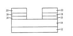
- FIG. 1illustrates a substrate fragment indicated generally with reference to numeral 10 at a preliminary processing stage.
- the substrate fragment 10 in progresscan comprise a semiconductor wafer substrate or the wafer along with various process layers formed thereon, including one or more semiconductor layers or other formations, and active or operable portions of semiconductor devices.
- the substrate fragment 10comprises a substrate 12 , a dielectric (silicon oxide) layer 14 to be etched, a hafnium aluminum oxide (HfAlO x ) layer 16 , a dielectric antireflective coating (DARC) layer 18 , and a photoresist masking layer 20 .
- the substrate 12is compositionally dissimilar to the silicon oxide layer 14 , and can be composed of a silicon layer such as monocrystalline, polycrystalline or amorphous silicon, a doped silicon region, a nitride material (e.g., silicon nitride such as Si 3 N 4 , a refractory metal nitride such as titanium nitride (TiN), tungsten nitride (WN), etc.), a silicon oxide layer with different doping than a silicon oxide dielectric layer 14 , a metal silicide such as titanium silicide (TiSi 2 ), a metal interconnect, or other material layer.
- a silicon layersuch as monocrystalline, polycrystalline or amorphous silicon
- a doped silicon regione.g., silicon nitride such as Si 3 N 4 , a refractory metal nitride such as titanium nitride (TiN), tungsten nitride (WN), etc.
- the dielectric layer 14can be formed of undoped or doped silicon oxide (SiO x ), for example, silicon oxide deposited from tetraethylorthosilicate (TEOS), borophosphosilicate glass (BPSG), borosilicate glass (BSG), phosphosilicate glass (PSG), spin-on-glass (SOG), etc., in a single layer or multiple layers.
- TEOStetraethylorthosilicate
- BPSGborophosphosilicate glass
- BSGborosilicate glass
- PSGphosphosilicate glass
- spin-on-glass (SOG)spin-on-glass
- the dielectric (SiO x ) layer 14will comprise, consist essentially of, or consist of silicon and oxygen.
- a typical thickness of the dielectric layer 14is about 1,000-20,000 ⁇ .
- a hafnium aluminum oxide layer 16(Hf x Al y O z or HfAlO x such as HfAlO 3 ), a high dielectric constant (high-k) material, replaces a conventional hard mask such as a carbon-based hard mask that is generally formed over a material to be etched.
- the HFAlO x layer 16is formed as a hard mask over the dielectric (SiO x ) layer 14 by atomic layer deposition (ALD) processing with a concentration ratio of Hf:Al in the film at about 20:1 to about 4:1 (wt-%), or about 10:1 to about 8:1 (ALD deposition temperature of about 300° C).
- the thickness of the HfAlO x hard mask layer 16is generally about 200-1,000 ⁇ , or about 300-500 ⁇ .
- the HFAlO x hard mask layer 16can be formed by ALD processing using known techniques in the art, for example, as described in U.S. Pat. No. 7,211,492 (Forbes et al.) and U.S. Pat. No. 7,135,421 (Ahn et al.), which are commonly assigned to Micron Technology, Inc., the disclosures of which are incorporated by reference herein.
- the HfAlO x hard mask layer 16can be formed using ALD processing by employing a hafnium sequence of pulsing a hafnium-containing precursor (e.g., HfCl 4 ) into a reaction chamber containing a substrate and pulsing a first oxygen-containing precursor (e.g., water vapor) into the reaction chamber as an oxidizing reactant to form hafnium oxide, and an aluminum sequence by pulsing an aluminum-containing precursor (e.g., trimethylaluminum, Al(CH 3 ) 3 , or DMEAA, an adduct of alane (AlH 3 ) and dimethylethylamine (N(CH 3 ) 2 (C 2 H 5 )), into the reaction chamber and pulsing a second oxygen containing precursor (e.g., distilled water vapor) into the reaction chamber as an oxidizing reactant to form a HfAlO x film.
- a hafnium-containing precursore.
- Each precursoris pulsed into the reaction chamber for a selected time period (pulse time), typically from about 0.5 seconds to about 2-3 seconds. Between each precursor pulsing, the reaction chamber is purged with an inert gas (e.g., nitrogen or argon) or evacuated to remove precursor excess and reaction by-products.
- an inert gase.g., nitrogen or argon
- the thickness of the HfAlO x filmis controlled by repeating for a number of cycles the pulsing of the Hf-containing precursor, the first O-containing precursor, the Al-containing precursor, and the second O-containing precursor until the desired thickness is formed.
- the HfAlO x hard mask layer 16can be engineered with selected characteristics by controlling precursor materials for each sequence, processing temperatures and pressures for each sequence, individual precursor pulsing times, and heat treatment at the end of the process, at the end of each cycle, and at the end of each sequence.
- the DARC layer 18can serve as an intermediate hard mask to reduce light reflections during lithography.
- the DARC layer 18can be deposited onto the HfAlO x hard mask layer 16 by known processes, such as chemical vapor deposition (CVD) or plasma enhanced CVD (PECVD) including, for example, electron cyclotron resonance (ECR) PECVD, and bias ECR PECVD processes, for example, using a feed gas that comprises SiH 4 , N 2 , O 2 , and argon.
- CVDchemical vapor deposition
- PECVDplasma enhanced CVD
- ECRelectron cyclotron resonance
- a typical thickness of the DARC layer 18is about 200-1,000 ⁇ , or about 300-400 ⁇ .
- a photoresist mask layer 20typically an organic polymeric material (e.g., a novolac resin), is formed over the DARC layer 18 and, as depicted, exposed and developed using conventional photolithographic techniques as known in the art, to provide a desired pattern with openings 22 that expose portions of the DARC layer 18 .
- organic polymeric materiale.g., a novolac resin
- the pattern in the photoresist mask layer 20can be transferred to the DARC layer 18 by a standard dry etch (arrows ⁇ ) using, for example, a fluorine-based gas plasma chemistry to expose the underlying HFAlO x hard mask layer 16 , as shown in FIG. 2 .
- the HFAlO x hard mask layer 16can be dry etched (arrows ⁇ ) using a standard chemistry to expose portions of the silicon oxide layer 14 .
- An etchant gasis used, for example, a mixture of boron trichloride (BCl 3 ) and chlorine (Cl 2 ) gases, which provides good selectivity to etch HfAlO x and stop on TEOS or other silicon oxide material (e.g., substrate 12 ).
- the dielectric (SiO x ) layer 14is then dry etched to form a contact opening 24 (i.e., contact hole, via, or other opening such as a trench) extending to the underlying substrate layer 12 for forming, for example, a contact hole for an interconnect level, a gate electrode, a capacitor electrode, a via, etc.
- a silicon oxide dry etchcan be conducted according to known methods using a standard fluorocarbon-based dry etch chemistry (e.g., CF 4 , CHF 3 , CH 2 F 2 , CH 3 F, C 2 F 6 , C 3 F 8 , C 4 F 6 , etc.).
- the contact opening 24is etched to a high aspect ratio of about 1:1 to about 20:1 with a width of about 15-65 nm and a depth of about 100 nm-2,000 nm, for example.
- the photoresist mask layer 20is selectively removed (dry stripped) as shown in FIG. 5 , for example, by a standard dry etch process using an oxygen (O 2 ) plasma ashing step.
- the DARC layer 18 and the HfAlO x hard mask layer 16are removed (stripped) selective to the dielectric (SiO x ) layer 14 and the substrate 12 , as illustrated in FIG. 6 .
- HfAlO x (and DARC) materialstypically use hydrofluoric acid (HF) based chemistries, e.g., a dilute HF/water wet etch.
- HFhydrofluoric acid
- standard dilute HF etch chemistriesare not selective to and will attack and rapidly etch silicon oxides such as BPSG, PSG and TEOS. This necessitates the use of different etch chemistries for stripping HfAlO x materials in the presence of oxides.
- the etchant compositions of the inventionare aqueous solutions of phosphoric acid (H 3 PO 4 ) and water (H 2 O) that etch HfAlO x material selective to silicon oxide (e.g., BPSG, PSG, TEOS, etc.).
- Embodiments of the etchant compositionsare formulated with a H 3 PO 4 :H 2 O volume ratio of about 50:50 to about 90:10, or about 80:20 to about 85:15, based on the total volume of the solution.
- a temperature range of about 100-185° C.is typical for most applications.
- the H 3 PO 4 :H 2 O etchant compositionsare maintained at a pH level ⁇ 2, which can be manipulated by adding an additional acid such HCl, H 2 SO 4 , HNO 3 , HCOOH and CH 3 COOH, among others.
- the etchant compositionconsists essentially of or consists of phosphoric acid and water, optionally with an additional acid in a minor but effective amount to modify the pH of the solution.
- the H 3 PO 4 /H 2 O etchant solutioncan be applied to the material layers, e.g., the HfAlO x layer 16 and DARC layer 18 , to be stripped in various ways.
- the etchant solutioncan be sprayed onto the substrate 10 , or the substrate can be dipped or immersed into a bath of the etchant solution (e.g., a megasonic bath), or the etchant solution can be flowed over the substrate, among other applications.
- the H 3 PO 4 /H 2 O etchant compositionsprovide a wet etch of HfAlO x (about 10:1 Hf:Al ratio) and DARC materials selective to the SiO x material layer 14 at an etch rate (or selectivity) of greater than 1, or an etch selectivity of about 2:1 to about 20:1 (HfAlO x :SiO x ), with little or no etching of the SiO x layer.
- Etchant compositions having a H 3 PO 4 :H 2 O volume ratio of about 50:50 to about 90:10provide an etch of ALD HfAlO x (Hf:Al ratio of about 20:1 to about 4:1) at a rate about 50-400 ⁇ /minute, an etch of a DARC material layer 18 at a rate of about 5-40 ⁇ /minute or about 20-40 ⁇ /minute, and minimal etching of a SiO x material layer 14 at about 5-40 ⁇ /minute or about 5-15 ⁇ /minute.
- an etchant solution of H 3 PO 4 :H 2 O at a ratio of about 80:20 to about 85:15 (v/v) (temperature of about 100-185° C.)will etch ALD HfAlO x (about 10:1 Hf:Al ratio) at an etch selectivity of about 8:1 to about 12:1.
- the application of an about 10:1 (v/v) H 3 PO 4 :H 2 O etchant solution at about 145° C.will provide an etch of an ALD HfAlO x film 16 (about 10:1 Hf:Al ratio) at a rate of about 300 ⁇ /minute.
- HfAlO x :PSGa selectivity to PSG of about 10:1 (HfAlO x :PSG), a selectivity to titanium nitride (TiN) of about 43:1 (HfAlO x :TiN), and a selectivity to silicon nitride (Si x N y , e.g., such as Si 3 N 4 ) of about 6:1 (HfAlO x :Si x N y ).
- the etchant solutioncan be used in applications for fabricating contact openings as illustrated, or other features such as word lines, digit lines, etc.
- the substrate 10can then undergo post-etch processing steps that are known in the art to fabricate desired components.
- the resulting contact openings 24can be further processed, for example, by filling with a metal or conductive material such as copper, aluminum, silicon, Ti 3 N 4 , among others, to form contacts or conductive lines, for example, to an underlying active area, contact, or conductive line, or with a metal-insulator-metal-stack to form capacitors with a dielectric material such as Al 2 O 3 , HfO 2 , ZrO 2 , SrTiO 3 , and the like, in the fabrication of integrated circuit devices such as memory devices. Finished semiconductor wafers can be cut into dies, which may then be further processed into integrated circuit chips and incorporated in electronic devices.
Landscapes
- Engineering & Computer Science (AREA)
- Chemical & Material Sciences (AREA)
- Microelectronics & Electronic Packaging (AREA)
- Power Engineering (AREA)
- Physics & Mathematics (AREA)
- Condensed Matter Physics & Semiconductors (AREA)
- General Physics & Mathematics (AREA)
- Computer Hardware Design (AREA)
- Inorganic Chemistry (AREA)
- Manufacturing & Machinery (AREA)
- Organic Chemistry (AREA)
- Materials Engineering (AREA)
- Chemical Kinetics & Catalysis (AREA)
- General Chemical & Material Sciences (AREA)
- Weting (AREA)
- Internal Circuitry In Semiconductor Integrated Circuit Devices (AREA)
Abstract
Description
Claims (22)
Priority Applications (3)
| Application Number | Priority Date | Filing Date | Title |
|---|---|---|---|
| US11/839,628US8283258B2 (en) | 2007-08-16 | 2007-08-16 | Selective wet etching of hafnium aluminum oxide films |
| US13/585,072US8618000B2 (en) | 2007-08-16 | 2012-08-14 | Selective wet etching of hafnium aluminum oxide films |
| US14/136,081US20140103498A1 (en) | 2007-08-16 | 2013-12-20 | Selective wet etching of hafnium aluminum oxide films |
Applications Claiming Priority (1)
| Application Number | Priority Date | Filing Date | Title |
|---|---|---|---|
| US11/839,628US8283258B2 (en) | 2007-08-16 | 2007-08-16 | Selective wet etching of hafnium aluminum oxide films |
Related Child Applications (1)
| Application Number | Title | Priority Date | Filing Date |
|---|---|---|---|
| US13/585,072ContinuationUS8618000B2 (en) | 2007-08-16 | 2012-08-14 | Selective wet etching of hafnium aluminum oxide films |
Publications (2)
| Publication Number | Publication Date |
|---|---|
| US20090047790A1 US20090047790A1 (en) | 2009-02-19 |
| US8283258B2true US8283258B2 (en) | 2012-10-09 |
Family
ID=40363306
Family Applications (3)
| Application Number | Title | Priority Date | Filing Date |
|---|---|---|---|
| US11/839,628Active2030-01-25US8283258B2 (en) | 2007-08-16 | 2007-08-16 | Selective wet etching of hafnium aluminum oxide films |
| US13/585,072ActiveUS8618000B2 (en) | 2007-08-16 | 2012-08-14 | Selective wet etching of hafnium aluminum oxide films |
| US14/136,081AbandonedUS20140103498A1 (en) | 2007-08-16 | 2013-12-20 | Selective wet etching of hafnium aluminum oxide films |
Family Applications After (2)
| Application Number | Title | Priority Date | Filing Date |
|---|---|---|---|
| US13/585,072ActiveUS8618000B2 (en) | 2007-08-16 | 2012-08-14 | Selective wet etching of hafnium aluminum oxide films |
| US14/136,081AbandonedUS20140103498A1 (en) | 2007-08-16 | 2013-12-20 | Selective wet etching of hafnium aluminum oxide films |
Country Status (1)
| Country | Link |
|---|---|
| US (3) | US8283258B2 (en) |
Cited By (4)
| Publication number | Priority date | Publication date | Assignee | Title |
|---|---|---|---|---|
| US20120306059A1 (en)* | 2007-08-16 | 2012-12-06 | Micron Technology, Inc. | Selective wet etching of hafnium aluminum oxide films |
| CN103146307A (en)* | 2013-03-28 | 2013-06-12 | 天津理工大学 | Nano polishing solution for chemical/mechanical polishing |
| CN104681424A (en)* | 2013-11-27 | 2015-06-03 | 中芯国际集成电路制造(上海)有限公司 | Forming method of transistor structure |
| US9362124B2 (en) | 2008-08-22 | 2016-06-07 | Taiwan Semiconductor Manufacturing Company, Ltd. | Method of patterning a metal gate of semiconductor device |
Families Citing this family (16)
| Publication number | Priority date | Publication date | Assignee | Title |
|---|---|---|---|---|
| US8334198B2 (en)* | 2011-04-12 | 2012-12-18 | Taiwan Semiconductor Manufacturing Company, Ltd. | Method of fabricating a plurality of gate structures |
| US9281203B2 (en)* | 2013-08-23 | 2016-03-08 | Taiwan Semiconductor Manufacturing Co., Ltd. | Silicon dot formation by direct self-assembly method for flash memory |
| US9064821B2 (en) | 2013-08-23 | 2015-06-23 | Taiwan Semiconductor Manufacturing Co. Ltd. | Silicon dot formation by self-assembly method and selective silicon growth for flash memory |
| US9859128B2 (en) | 2015-11-20 | 2018-01-02 | Applied Materials, Inc. | Self-aligned shielding of silicon oxide |
| US9875907B2 (en) | 2015-11-20 | 2018-01-23 | Applied Materials, Inc. | Self-aligned shielding of silicon oxide |
| US10358719B2 (en)* | 2016-11-23 | 2019-07-23 | Applied Materials, Inc. | Selective deposition of aluminum oxide on metal surfaces |
| SG11202102268VA (en)* | 2018-09-25 | 2021-04-29 | Hoya Corp | Mask blank, transfer mask, and method of manufacturing semiconductor device |
| US20220043335A1 (en)* | 2018-09-27 | 2022-02-10 | Hoya Corporation | Mask blank, transfer mask, and semiconductor-device manufacturing method |
| US12243752B2 (en) | 2018-11-15 | 2025-03-04 | Tokyo Electron Limited | Systems for etching a substrate using a hybrid wet atomic layer etching process |
| US11437250B2 (en)* | 2018-11-15 | 2022-09-06 | Tokyo Electron Limited | Processing system and platform for wet atomic layer etching using self-limiting and solubility-limited reactions |
| CN112047294B (en)* | 2020-08-31 | 2024-01-23 | 上海华虹宏力半导体制造有限公司 | Infrared MEMS bridge column structure and process method |
| US11915941B2 (en) | 2021-02-11 | 2024-02-27 | Tokyo Electron Limited | Dynamically adjusted purge timing in wet atomic layer etching |
| US11901436B2 (en)* | 2021-03-05 | 2024-02-13 | Taiwan Semiconductor Manufacturing Company, Ltd. | Formation of transistor gates |
| US11802342B2 (en) | 2021-10-19 | 2023-10-31 | Tokyo Electron Limited | Methods for wet atomic layer etching of ruthenium |
| US12276033B2 (en) | 2021-10-19 | 2025-04-15 | Tokyo Electron Limited | Methods for wet etching of noble metals |
| US11866831B2 (en) | 2021-11-09 | 2024-01-09 | Tokyo Electron Limited | Methods for wet atomic layer etching of copper |
Citations (118)
| Publication number | Priority date | Publication date | Assignee | Title |
|---|---|---|---|---|
| US4877647A (en) | 1986-04-17 | 1989-10-31 | Kansas State University Research Foundation | Method of coating substrates with solvated clusters of metal particles |
| US5482656A (en) | 1993-03-04 | 1996-01-09 | Kabushiki Kaisha Toshiba | Non-linear optical devices employing a polysilane composition and a polysilane composition therefor |
| US5538655A (en) | 1994-06-29 | 1996-07-23 | Arthur D. Little, Inc. | Molecular complexes for use as electrolyte components |
| US5622668A (en) | 1992-02-07 | 1997-04-22 | The United States Of America As Represented By The Secretary Of The Air Force | Method for preparing oriented polymer structures and said structures |
| US5948470A (en) | 1997-04-28 | 1999-09-07 | Harrison; Christopher | Method of nanoscale patterning and products made thereby |
| EP0784543B1 (en) | 1995-08-04 | 2000-04-26 | International Business Machines Corporation | Lithographic surface or thin layer modification |
| US6103632A (en) | 1997-10-22 | 2000-08-15 | Applied Material Inc. | In situ Etching of inorganic dielectric anti-reflective coating from a substrate |
| US6111323A (en) | 1997-12-30 | 2000-08-29 | International Business Machines Corporation | Reworkable thermoplastic encapsulant |
| US6143647A (en) | 1997-07-24 | 2000-11-07 | Intel Corporation | Silicon-rich block copolymers to achieve unbalanced vias |
| US6156149A (en) | 1997-05-07 | 2000-12-05 | Applied Materials, Inc. | In situ deposition of a dielectric oxide layer and anti-reflective coating |
| US6200909B1 (en) | 1998-03-13 | 2001-03-13 | Micron Technology Inc. | Method for selective etching of antireflective coatings |
| US6403382B1 (en) | 1998-12-08 | 2002-06-11 | Regents Of The University Of Minnesota | Attachment chemistry for organic molecules to silicon |
| US6423465B1 (en) | 2000-01-28 | 2002-07-23 | International Business Machines Corporation | Process for preparing a patterned continuous polymeric brush on a substrate surface |
| US6503841B1 (en) | 2000-07-07 | 2003-01-07 | Agere Systems Inc. | Oxide etch |
| US6548830B1 (en) | 1996-05-22 | 2003-04-15 | Sony Corporation | Semiconductor device formed of single crystal grains in a grid pattern |
| US20030091752A1 (en) | 2001-10-05 | 2003-05-15 | Nealey Paul F. | Guided self-assembly of block copolymer films on interferometrically nanopatterned substrates |
| US6566248B1 (en) | 2001-01-11 | 2003-05-20 | Advanced Micro Devices, Inc. | Graphoepitaxial conductor cores in integrated circuit interconnects |
| US6565763B1 (en) | 1999-06-07 | 2003-05-20 | Kabushiki Kaisha Toshiba | Method for manufacturing porous structure and method for forming pattern |
| US6569528B2 (en) | 2001-06-23 | 2003-05-27 | Pacific Corporation | Amphiphilic biodegradable block copolymers and self-assembled polymer aggregates formed from the same in aqueous milieu |
| US6569774B1 (en) | 2000-08-31 | 2003-05-27 | Micron Technology, Inc. | Method to eliminate striations and surface roughness caused by dry etch |
| US20030100822A1 (en) | 2001-09-01 | 2003-05-29 | Seok Lew | Analyte measuring biosensor chip using image scanning system |
| US20030178707A1 (en) | 2002-03-21 | 2003-09-25 | Abbott Donald C. | Preplated stamped small outline no-lead leadframes having etched profiles |
| US20030185741A1 (en) | 2001-04-06 | 2003-10-02 | Krzysztof Matyjaszewski | Process for the preparation of nanostructured materials |
| US20030235985A1 (en)* | 2002-06-14 | 2003-12-25 | Christenson Kurt K. | Method for etching high-k films in solutions comprising dilute fluoride species |
| US6689473B2 (en) | 2001-07-17 | 2004-02-10 | Surmodics, Inc. | Self assembling monolayer compositions |
| EP1416303A2 (en) | 2002-10-30 | 2004-05-06 | Hitachi, Ltd. | Functioning substrate with a group of columnar micro pillars and its manufacturing method |
| US20040127001A1 (en) | 2002-12-27 | 2004-07-01 | International Business Machines Corporation | Robust ultra-low k interconnect structures using bridge-then-metallization fabrication sequence |
| US20040124092A1 (en) | 2002-12-30 | 2004-07-01 | Black Charles T. | Inorganic nanoporous membranes and methods to form same |
| US20040142578A1 (en) | 2002-03-28 | 2004-07-22 | Ulrich Wiesner | Thin film nanostructures |
| US6781166B2 (en) | 1999-07-02 | 2004-08-24 | President & Fellows Of Harvard College | Nanoscopic wire-based devices and arrays |
| US20040209194A1 (en)* | 2003-03-25 | 2004-10-21 | Semiconductor Leading Edge Technologies, Inc. | Ultraviolet-light radiating apparatus, wet etching apparatus and wet etching method using ultravioletlight, and method of manufacturing semiconductor device |
| US20040222415A1 (en) | 2003-03-11 | 2004-11-11 | Industrial Technology Research Institute | Organic device including semiconducting layer aligned according to microgrooves of photoresist layer |
| US20040254317A1 (en) | 2003-06-12 | 2004-12-16 | Jinlian Hu | Methods for producing di-block polymers |
| US20040256615A1 (en) | 2001-07-09 | 2004-12-23 | Henning Sirringhaus | Lamellar polymer architecture |
| US20040265548A1 (en) | 2003-05-20 | 2004-12-30 | Rong-Ming Ho | Nanopatterned templates from oriented degradable diblock copolymer thin films |
| CN1562730A (en) | 2004-03-24 | 2005-01-12 | 哈尔滨工业大学 | Method for adjusting and controlling configuration of self-assembling block copolymer template oriented to nano micro machining |
| JP2005008882A (en) | 1999-06-07 | 2005-01-13 | Toshiba Corp | Porous structure manufacturing method, porous structure forming material, pattern forming method, pattern forming material, electrochemical cell, and hollow fiber filter |
| US20050019498A1 (en)* | 2003-07-15 | 2005-01-27 | Dainippon Screen Mfg. Co., Ltd. | Substrate treating method and apparatus |
| US20050062165A1 (en) | 2003-09-19 | 2005-03-24 | International Business Machines Corporation | Method of forming closed air gap interconnects and structures formed thereby |
| US20050067704A1 (en)* | 2003-09-26 | 2005-03-31 | Akio Kaneko | Semiconductor device and method of manufacturing the same |
| US20050074706A1 (en) | 2003-10-06 | 2005-04-07 | Robert Bristol | Enhancing photoresist performance using electric fields |
| US6890624B1 (en) | 2000-04-25 | 2005-05-10 | Nanogram Corporation | Self-assembled structures |
| US6890703B2 (en) | 2002-03-06 | 2005-05-10 | International Business Machines Corporation | Preparation of crosslinked particles from polymers having activatible crosslinking groups |
| US20050100830A1 (en) | 2003-10-27 | 2005-05-12 | Molecular Imprints, Inc. | Methods for fabricating patterned features utilizing imprint lithography |
| US20050124135A1 (en) | 2003-11-25 | 2005-06-09 | Farrokh Ayazi | Methods of forming oxide masks with submicron openings and microstructures formed thereby |
| US20050145959A1 (en)* | 2001-03-15 | 2005-07-07 | Leonard Forbes | Technique to mitigate short channel effects with vertical gate transistor with different gate materials |
| US6924341B2 (en) | 2001-03-30 | 2005-08-02 | The Uab Research Foundation | Polymer formation in room temperature ionic liquids |
| US20050208752A1 (en) | 2004-03-19 | 2005-09-22 | Colburn Matthew E | Method for fabricating a self-aligned nanocolumnar airbridge and structure produced thereby |
| US6949456B2 (en) | 2002-10-31 | 2005-09-27 | Asm Japan K.K. | Method for manufacturing semiconductor device having porous structure with air-gaps |
| US20050227473A1 (en)* | 2004-03-24 | 2005-10-13 | Tosoh Corporation | Etching composition and method for etching a substrate |
| US20050238889A1 (en) | 2003-07-10 | 2005-10-27 | Nancy Iwamoto | Layered components, materials, methods of production and uses thereof |
| US20050250053A1 (en) | 2004-05-06 | 2005-11-10 | Marsh Eugene P | Selective provision of a diblock copolymer material |
| WO2005122285A2 (en) | 2004-06-04 | 2005-12-22 | The Board Of Trustees Of The University Of Illinois | Methods and devices for fabricating and assembling printable semiconductor elements |
| US20060014001A1 (en) | 2000-05-26 | 2006-01-19 | Hua Zhang | Fabrication of sub-50 nm solid-state nanostructures based on nanolithography |
| JP2006036923A (en) | 2004-07-27 | 2006-02-09 | National Institute Of Advanced Industrial & Technology | Highly oriented film of block copolymer-clay nanocomposite and method for producing the same |
| JP2006055982A (en) | 2004-08-23 | 2006-03-02 | Ind Technol Res Inst | Nanopatterned templates from organized degradation diblock copolymer thin films |
| US20060046079A1 (en) | 2004-09-01 | 2006-03-02 | Samsung Corning Co., Ltd. | Method for preparing surfactant-templated, mesoporous low dielectric film |
| US20060062867A1 (en) | 2002-07-11 | 2006-03-23 | Molecular Imprints, Inc. | Formation of discontinuous films during an imprint lithography process |
| US20060078681A1 (en) | 2004-10-13 | 2006-04-13 | Kabushiki Kaisha Toshiba | Pattern forming method and method of processing a structure by use of same |
| US20060094199A1 (en) | 2004-10-29 | 2006-05-04 | Deok Sin Kil | Method for forming capacitor of semiconductor device |
| US7045851B2 (en) | 2003-06-20 | 2006-05-16 | International Business Machines Corporation | Nonvolatile memory device using semiconductor nanocrystals and method of forming same |
| US20060105562A1 (en) | 2004-11-12 | 2006-05-18 | Seagate Technology Llc | Method to make nano structure below 25 nanometer with high uniformity on large scale |
| US7056849B2 (en) | 2004-01-16 | 2006-06-06 | General Electric Company | Nanoscale ordered composites of covalent ceramics for high-temperature structural applications via block-copolymer-assisted assembly and method of making |
| US20060124467A1 (en) | 2003-05-20 | 2006-06-15 | Industrial Technology Research Institute | Metal nanodot arrays and fabrication methods thereof |
| US20060134556A1 (en) | 2004-11-22 | 2006-06-22 | Wisconsin Alumni Research Foundation | Methods and compositions for forming aperiodic patterned copolymer films |
| WO2006076016A2 (en) | 2004-05-21 | 2006-07-20 | Krzysztof Matyjaszewski | Conducting polymers |
| WO2006078952A1 (en) | 2005-01-21 | 2006-07-27 | University Of California | Methods for fabricating a long-range ordered periodic array of nano-features, and articles comprising same |
| US20060192283A1 (en) | 2004-04-29 | 2006-08-31 | Benson Peter A | Semiconductor wafer assemblies |
| US20060205875A1 (en) | 2005-03-11 | 2006-09-14 | Cha Jennifer N | Materials having predefined morphologies and methods of formation thereof |
| US20060217285A1 (en) | 2002-11-07 | 2006-09-28 | Mathias Destarac | Controlled structure copolymer comprising an amphoteric or zwitterionic part |
| US20060216888A1 (en)* | 2005-03-23 | 2006-09-28 | Wei Zheng | High K stack for non-volatile memory |
| US7115995B2 (en) | 2000-12-20 | 2006-10-03 | Intel Corporation | Structural reinforcement of highly porous low k dielectric films by Cu diffusion barrier structures |
| US7118784B1 (en) | 2005-06-27 | 2006-10-10 | The Regents Of The University Of California | Method and apparatus for controlling nucleation in self-assembled films |
| US7132370B2 (en) | 2003-08-01 | 2006-11-07 | Interuniversitair Microelektronica Centrum (Imec) | Method for selective removal of high-k material |
| US20060249784A1 (en) | 2005-05-06 | 2006-11-09 | International Business Machines Corporation | Field effect transistor device including an array of channel elements and methods for forming |
| US7135421B2 (en) | 2002-06-05 | 2006-11-14 | Micron Technology, Inc. | Atomic layer-deposited hafnium aluminum oxide |
| US7135523B2 (en) | 2003-03-14 | 2006-11-14 | Industrial Technology Research Institute | Nanoscale helical microstructures and channels from chiral poly(L-lactide) block containing block copolymers |
| US20060258159A1 (en) | 2005-05-16 | 2006-11-16 | International Business Machines Corporation | Process for preparing electronics structures using a sacrificial multilayer hardmask scheme |
| US20060276048A1 (en) | 2005-06-07 | 2006-12-07 | Micron Technology, Inc. | Methods of etching nickel silicide and cobalt silicide and methods of forming conductive lines |
| US20060281266A1 (en) | 2005-06-09 | 2006-12-14 | Wells David H | Method and apparatus for adjusting feature size and position |
| US20060278158A1 (en) | 2005-06-08 | 2006-12-14 | Tolbert Sarah H | Ordered vertically oriented porous inorganic films produced through solution processing |
| US20070007602A1 (en) | 2005-07-11 | 2007-01-11 | Renesas Technology Corp. | Semiconductor device which has MOS structure and method of manufacturing the same |
| US7163712B2 (en) | 2000-03-03 | 2007-01-16 | Duke University | Microstamping activated polymer surfaces |
| US20070020749A1 (en) | 2005-03-23 | 2007-01-25 | Wisconsin Alumni Research Foundation | Materials and methods for creating imaging layers |
| US20070023805A1 (en) | 2005-07-26 | 2007-02-01 | Wells David H | Reverse construction memory cell |
| US20070045562A1 (en) | 2005-08-29 | 2007-03-01 | Micron Technology, Inc. | Systems and methods for controlling ambient pressure during processing of microfeature workpieces, including during immersion lithography |
| US20070048674A1 (en) | 2005-09-01 | 2007-03-01 | Wells David H | Methods for forming arrays of small, closely spaced features |
| US20070049045A1 (en) | 2005-07-11 | 2007-03-01 | Paul Zimmerman | Atomic layer deposition method for depositing a layer |
| US20070048941A1 (en) | 2005-09-01 | 2007-03-01 | Micron Technology, Inc. | Transistor gate forming methods and transistor structures |
| US20070048976A1 (en) | 2005-08-31 | 2007-03-01 | Prashant Raghu | Methods of forming semiconductor constructions and capacitors |
| WO2007024323A2 (en) | 2005-06-17 | 2007-03-01 | The University Of North Carolina At Chapel Hill | Nanoparticle fabrication methods, systems, and materials |
| US7186613B2 (en) | 2002-05-30 | 2007-03-06 | Air Products And Chemicals, Inc. | Low dielectric materials and methods for making same |
| US7189435B2 (en) | 2001-03-14 | 2007-03-13 | University Of Massachusetts | Nanofabrication |
| US7190049B2 (en) | 2000-03-22 | 2007-03-13 | University Of Massachusetts | Nanocylinder arrays |
| US7189430B2 (en) | 2002-02-11 | 2007-03-13 | Rensselaer Polytechnic Institute | Directed assembly of highly-organized carbon nanotube architectures |
| US20070059929A1 (en)* | 2004-06-25 | 2007-03-15 | Hag-Ju Cho | Method of forming a tantalum carbon nitride layer and method of manufacturing a semiconductor device using the same |
| US20070071881A1 (en) | 2003-08-11 | 2007-03-29 | Lay-Lay Chua | Method of making a polymer device |
| US20070072403A1 (en) | 2005-09-27 | 2007-03-29 | Oki Electric Industry Co., Ltd. | Semiconductor device and method for fabricating the same |
| US7202308B2 (en) | 2000-12-21 | 2007-04-10 | Atofina | Hydrogenation method for unsaturated block copolymers and hydrogenated unsaturated block copolymers |
| WO2007024241A3 (en) | 2004-09-10 | 2007-04-12 | Ut Battelle Llc | Highly ordered porous carbon materials having well defined nanostructures and method of synthesis |
| US7211492B2 (en) | 2005-07-07 | 2007-05-01 | Micron Technology, Inc. | Self aligned metal gates on high-k dielectrics |
| WO2007019439A3 (en) | 2005-08-04 | 2007-05-03 | Angiotech Int Ag | Block copolymer compositions and uses thereof |
| WO2007055041A1 (en) | 2005-11-10 | 2007-05-18 | National University Corporation Kyoto Institute Of Technology | Membrane of block copolymer with oriented cylinder structure and process for producing the same |
| US20070122932A1 (en) | 2001-10-05 | 2007-05-31 | Cabot Corporation | Methods and compositions for the formation of recessed electrical features on a substrate |
| US20070132004A1 (en) | 2005-10-14 | 2007-06-14 | Naoki Yasuda | Nonvolatile semiconductor memory device |
| US20070145009A1 (en) | 2005-07-27 | 2007-06-28 | Micron Technology, Inc. | Etch Compositions and Methods of Processing a Substrate |
| US20070175859A1 (en) | 2006-02-02 | 2007-08-02 | International Business Machines Corporation | Methods for forming improved self-assembled patterns of block copolymers |
| US20070181870A1 (en) | 2006-01-18 | 2007-08-09 | Consiglio Nazionale Delle Ricerche | Nanometric Device for the Measurement of the Conductivity and Quantum Effects of Individual Molecules and Methods for the Manufacture and Use Thereof |
| US20070208159A1 (en) | 2006-03-02 | 2007-09-06 | General Electric Company | Poly(arylene ether) block copolymer compositions, methods, and articles |
| US20070224819A1 (en) | 2006-03-23 | 2007-09-27 | Micron Technology, Inc. | Topography directed patterning |
| US20070227383A1 (en) | 2004-06-30 | 2007-10-04 | Koninklijke Philips Electronics, N.V. | Soft Lithographic Stamp with a Chemically Patterned Surface |
| US20070249117A1 (en) | 2006-04-19 | 2007-10-25 | Kang Kyong-Rim | Polymer resin composition, related method for forming a pattern, and related method for fabricating a capacitor |
| US20080064220A1 (en)* | 2006-09-12 | 2008-03-13 | Tokyo Electron Limited | Method and system for dry etching a hafnium containing material |
| US20080103256A1 (en) | 2006-10-30 | 2008-05-01 | Kim Ho-Cheol | Self-assembled lamellar microdomains and method of alignment |
| US20080164558A1 (en) | 2007-01-09 | 2008-07-10 | International Business Machines Corporation | Method for fabricating shallow trench isolation structures using diblock copolymer patterning |
| WO2008091741A2 (en) | 2007-01-24 | 2008-07-31 | Micron Technology, Inc. | Two-dimensional arrays of holes with sub-lithographic diameters formed by block copolymer self-assembly |
| WO2008097736A2 (en) | 2007-02-08 | 2008-08-14 | Micron Technology, Inc. | Methods using block copolymer self-assembly for sub-lithographic patterning |
| WO2008124219A2 (en) | 2007-03-06 | 2008-10-16 | Micron Technology, Inc. | Registered structure formation via the apllication of directed thermal energy to diblock copolymer films |
Family Cites Families (16)
| Publication number | Priority date | Publication date | Assignee | Title |
|---|---|---|---|---|
| US703495A (en)* | 1901-12-11 | 1902-07-01 | Louis Joseph Anton Staniewicz | Bookbinder's clamp. |
| US6268282B1 (en)* | 1998-09-03 | 2001-07-31 | Micron Technology, Inc. | Semiconductor processing methods of forming and utilizing antireflective material layers, and methods of forming transistor gate stacks |
| GR1004325B (en)* | 2000-07-03 | 2003-09-05 | Electroacoustic tranducer with field replaceable diaphragm crrying two interlaced coils | |
| KR100370241B1 (en)* | 2000-10-31 | 2003-01-30 | 삼성전자 주식회사 | Conducting line of semiconductor device using aluminum oxide as a hard mask and manufacturing method thereof |
| US6812043B2 (en)* | 2002-04-25 | 2004-11-02 | Taiwan Semiconductor Manufacturing Co., Ltd. | Method for forming a carbon doped oxide low-k insulating layer |
| US6939794B2 (en)* | 2003-06-17 | 2005-09-06 | Micron Technology, Inc. | Boron-doped amorphous carbon film for use as a hard etch mask during the formation of a semiconductor device |
| DE10338422B4 (en)* | 2003-08-18 | 2007-08-16 | Infineon Technologies Ag | Selective plasma etching process for alumina structuring and its use |
| KR100590583B1 (en)* | 2003-09-15 | 2006-06-15 | 에스케이 텔레콤주식회사 | How to play mobile game using mobile terminal and electronic compass module with electronic compass module |
| US7141511B2 (en)* | 2004-04-27 | 2006-11-28 | Micron Technology Inc. | Method and apparatus for fabricating a memory device with a dielectric etch stop layer |
| US20060030495A1 (en)* | 2004-08-06 | 2006-02-09 | Gregg George L Jr | Bullet lubrication formula |
| US7910288B2 (en)* | 2004-09-01 | 2011-03-22 | Micron Technology, Inc. | Mask material conversion |
| US20070099422A1 (en)* | 2005-10-28 | 2007-05-03 | Kapila Wijekoon | Process for electroless copper deposition |
| KR100684888B1 (en)* | 2005-11-11 | 2007-02-20 | 삼성전자주식회사 | Nonvolatile Memory Device and Manufacturing Method Thereof |
| US7602068B2 (en)* | 2006-01-19 | 2009-10-13 | International Machines Corporation | Dual-damascene process to fabricate thick wire structure |
| US7960797B2 (en)* | 2006-08-29 | 2011-06-14 | Micron Technology, Inc. | Semiconductor devices including fine pitch arrays with staggered contacts |
| US8283258B2 (en)* | 2007-08-16 | 2012-10-09 | Micron Technology, Inc. | Selective wet etching of hafnium aluminum oxide films |
- 2007
- 2007-08-16USUS11/839,628patent/US8283258B2/enactiveActive
- 2012
- 2012-08-14USUS13/585,072patent/US8618000B2/enactiveActive
- 2013
- 2013-12-20USUS14/136,081patent/US20140103498A1/ennot_activeAbandoned
Patent Citations (130)
| Publication number | Priority date | Publication date | Assignee | Title |
|---|---|---|---|---|
| US4877647A (en) | 1986-04-17 | 1989-10-31 | Kansas State University Research Foundation | Method of coating substrates with solvated clusters of metal particles |
| US5622668A (en) | 1992-02-07 | 1997-04-22 | The United States Of America As Represented By The Secretary Of The Air Force | Method for preparing oriented polymer structures and said structures |
| US5482656A (en) | 1993-03-04 | 1996-01-09 | Kabushiki Kaisha Toshiba | Non-linear optical devices employing a polysilane composition and a polysilane composition therefor |
| US5538655A (en) | 1994-06-29 | 1996-07-23 | Arthur D. Little, Inc. | Molecular complexes for use as electrolyte components |
| EP0784543B1 (en) | 1995-08-04 | 2000-04-26 | International Business Machines Corporation | Lithographic surface or thin layer modification |
| US6548830B1 (en) | 1996-05-22 | 2003-04-15 | Sony Corporation | Semiconductor device formed of single crystal grains in a grid pattern |
| US5948470A (en) | 1997-04-28 | 1999-09-07 | Harrison; Christopher | Method of nanoscale patterning and products made thereby |
| US6156149A (en) | 1997-05-07 | 2000-12-05 | Applied Materials, Inc. | In situ deposition of a dielectric oxide layer and anti-reflective coating |
| US6143647A (en) | 1997-07-24 | 2000-11-07 | Intel Corporation | Silicon-rich block copolymers to achieve unbalanced vias |
| US6103632A (en) | 1997-10-22 | 2000-08-15 | Applied Material Inc. | In situ Etching of inorganic dielectric anti-reflective coating from a substrate |
| US6111323A (en) | 1997-12-30 | 2000-08-29 | International Business Machines Corporation | Reworkable thermoplastic encapsulant |
| US6200909B1 (en) | 1998-03-13 | 2001-03-13 | Micron Technology Inc. | Method for selective etching of antireflective coatings |
| US6403382B1 (en) | 1998-12-08 | 2002-06-11 | Regents Of The University Of Minnesota | Attachment chemistry for organic molecules to silicon |
| JP2005008882A (en) | 1999-06-07 | 2005-01-13 | Toshiba Corp | Porous structure manufacturing method, porous structure forming material, pattern forming method, pattern forming material, electrochemical cell, and hollow fiber filter |
| US6565763B1 (en) | 1999-06-07 | 2003-05-20 | Kabushiki Kaisha Toshiba | Method for manufacturing porous structure and method for forming pattern |
| US7172953B2 (en) | 1999-07-02 | 2007-02-06 | President And Fellows Of Harvard College | Methods of forming nanoscopic wire-based devices and arrays |
| US6781166B2 (en) | 1999-07-02 | 2004-08-24 | President & Fellows Of Harvard College | Nanoscopic wire-based devices and arrays |
| US6423465B1 (en) | 2000-01-28 | 2002-07-23 | International Business Machines Corporation | Process for preparing a patterned continuous polymeric brush on a substrate surface |
| US7163712B2 (en) | 2000-03-03 | 2007-01-16 | Duke University | Microstamping activated polymer surfaces |
| US7190049B2 (en) | 2000-03-22 | 2007-03-13 | University Of Massachusetts | Nanocylinder arrays |
| US6890624B1 (en) | 2000-04-25 | 2005-05-10 | Nanogram Corporation | Self-assembled structures |
| US20060014001A1 (en) | 2000-05-26 | 2006-01-19 | Hua Zhang | Fabrication of sub-50 nm solid-state nanostructures based on nanolithography |
| US7291284B2 (en) | 2000-05-26 | 2007-11-06 | Northwestern University | Fabrication of sub-50 nm solid-state nanostructures based on nanolithography |
| US6503841B1 (en) | 2000-07-07 | 2003-01-07 | Agere Systems Inc. | Oxide etch |
| US6569774B1 (en) | 2000-08-31 | 2003-05-27 | Micron Technology, Inc. | Method to eliminate striations and surface roughness caused by dry etch |
| US7115995B2 (en) | 2000-12-20 | 2006-10-03 | Intel Corporation | Structural reinforcement of highly porous low k dielectric films by Cu diffusion barrier structures |
| US7202308B2 (en) | 2000-12-21 | 2007-04-10 | Atofina | Hydrogenation method for unsaturated block copolymers and hydrogenated unsaturated block copolymers |
| US6566248B1 (en) | 2001-01-11 | 2003-05-20 | Advanced Micro Devices, Inc. | Graphoepitaxial conductor cores in integrated circuit interconnects |
| US7189435B2 (en) | 2001-03-14 | 2007-03-13 | University Of Massachusetts | Nanofabrication |
| US20070200477A1 (en) | 2001-03-14 | 2007-08-30 | University Of Massachusetts | Nanofabrication |
| US20050145959A1 (en)* | 2001-03-15 | 2005-07-07 | Leonard Forbes | Technique to mitigate short channel effects with vertical gate transistor with different gate materials |
| US6924341B2 (en) | 2001-03-30 | 2005-08-02 | The Uab Research Foundation | Polymer formation in room temperature ionic liquids |
| US7056455B2 (en) | 2001-04-06 | 2006-06-06 | Carnegie Mellon University | Process for the preparation of nanostructured materials |
| US20030185741A1 (en) | 2001-04-06 | 2003-10-02 | Krzysztof Matyjaszewski | Process for the preparation of nanostructured materials |
| US6569528B2 (en) | 2001-06-23 | 2003-05-27 | Pacific Corporation | Amphiphilic biodegradable block copolymers and self-assembled polymer aggregates formed from the same in aqueous milieu |
| US20040256615A1 (en) | 2001-07-09 | 2004-12-23 | Henning Sirringhaus | Lamellar polymer architecture |
| US6689473B2 (en) | 2001-07-17 | 2004-02-10 | Surmodics, Inc. | Self assembling monolayer compositions |
| US20030100822A1 (en) | 2001-09-01 | 2003-05-29 | Seok Lew | Analyte measuring biosensor chip using image scanning system |
| US6746825B2 (en) | 2001-10-05 | 2004-06-08 | Wisconsin Alumni Research Foundation | Guided self-assembly of block copolymer films on interferometrically nanopatterned substrates |
| US20070122932A1 (en) | 2001-10-05 | 2007-05-31 | Cabot Corporation | Methods and compositions for the formation of recessed electrical features on a substrate |
| US20030091752A1 (en) | 2001-10-05 | 2003-05-15 | Nealey Paul F. | Guided self-assembly of block copolymer films on interferometrically nanopatterned substrates |
| US6926953B2 (en) | 2001-10-05 | 2005-08-09 | Wisconsin Alumni Research Foundation | Guided self-assembly of block copolymer films on interferometrically nanopatterned substrates |
| US7189430B2 (en) | 2002-02-11 | 2007-03-13 | Rensselaer Polytechnic Institute | Directed assembly of highly-organized carbon nanotube architectures |
| US6992115B2 (en) | 2002-03-06 | 2006-01-31 | International Business Machines Corporation | Preparation of crosslinked particles from polymers having activatible crosslinking groups |
| US6890703B2 (en) | 2002-03-06 | 2005-05-10 | International Business Machines Corporation | Preparation of crosslinked particles from polymers having activatible crosslinking groups |
| US20030178707A1 (en) | 2002-03-21 | 2003-09-25 | Abbott Donald C. | Preplated stamped small outline no-lead leadframes having etched profiles |
| US20040142578A1 (en) | 2002-03-28 | 2004-07-22 | Ulrich Wiesner | Thin film nanostructures |
| US7186613B2 (en) | 2002-05-30 | 2007-03-06 | Air Products And Chemicals, Inc. | Low dielectric materials and methods for making same |
| US7135421B2 (en) | 2002-06-05 | 2006-11-14 | Micron Technology, Inc. | Atomic layer-deposited hafnium aluminum oxide |
| US20030235985A1 (en)* | 2002-06-14 | 2003-12-25 | Christenson Kurt K. | Method for etching high-k films in solutions comprising dilute fluoride species |
| US20060062867A1 (en) | 2002-07-11 | 2006-03-23 | Molecular Imprints, Inc. | Formation of discontinuous films during an imprint lithography process |
| EP1416303A2 (en) | 2002-10-30 | 2004-05-06 | Hitachi, Ltd. | Functioning substrate with a group of columnar micro pillars and its manufacturing method |
| US6949456B2 (en) | 2002-10-31 | 2005-09-27 | Asm Japan K.K. | Method for manufacturing semiconductor device having porous structure with air-gaps |
| US20060217285A1 (en) | 2002-11-07 | 2006-09-28 | Mathias Destarac | Controlled structure copolymer comprising an amphoteric or zwitterionic part |
| US20040127001A1 (en) | 2002-12-27 | 2004-07-01 | International Business Machines Corporation | Robust ultra-low k interconnect structures using bridge-then-metallization fabrication sequence |
| US20040124092A1 (en) | 2002-12-30 | 2004-07-01 | Black Charles T. | Inorganic nanoporous membranes and methods to form same |
| US20040222415A1 (en) | 2003-03-11 | 2004-11-11 | Industrial Technology Research Institute | Organic device including semiconducting layer aligned according to microgrooves of photoresist layer |
| US7135523B2 (en) | 2003-03-14 | 2006-11-14 | Industrial Technology Research Institute | Nanoscale helical microstructures and channels from chiral poly(L-lactide) block containing block copolymers |
| US20040209194A1 (en)* | 2003-03-25 | 2004-10-21 | Semiconductor Leading Edge Technologies, Inc. | Ultraviolet-light radiating apparatus, wet etching apparatus and wet etching method using ultravioletlight, and method of manufacturing semiconductor device |
| US20040265548A1 (en) | 2003-05-20 | 2004-12-30 | Rong-Ming Ho | Nanopatterned templates from oriented degradable diblock copolymer thin films |
| US20060124467A1 (en) | 2003-05-20 | 2006-06-15 | Industrial Technology Research Institute | Metal nanodot arrays and fabrication methods thereof |
| US6989426B2 (en) | 2003-06-12 | 2006-01-24 | The Hong Kong Polytechnic University | Methods for producing di-block polymers |
| US20040254317A1 (en) | 2003-06-12 | 2004-12-16 | Jinlian Hu | Methods for producing di-block polymers |
| US20060163646A1 (en) | 2003-06-20 | 2006-07-27 | International Business Machines Corporation | Nonvolatile memory device using semiconductor nanocrystals and method of forming same |
| US7045851B2 (en) | 2003-06-20 | 2006-05-16 | International Business Machines Corporation | Nonvolatile memory device using semiconductor nanocrystals and method of forming same |
| US20050238889A1 (en) | 2003-07-10 | 2005-10-27 | Nancy Iwamoto | Layered components, materials, methods of production and uses thereof |
| US20050019498A1 (en)* | 2003-07-15 | 2005-01-27 | Dainippon Screen Mfg. Co., Ltd. | Substrate treating method and apparatus |
| US7132370B2 (en) | 2003-08-01 | 2006-11-07 | Interuniversitair Microelektronica Centrum (Imec) | Method for selective removal of high-k material |
| US20070071881A1 (en) | 2003-08-11 | 2007-03-29 | Lay-Lay Chua | Method of making a polymer device |
| US20050062165A1 (en) | 2003-09-19 | 2005-03-24 | International Business Machines Corporation | Method of forming closed air gap interconnects and structures formed thereby |
| US20050067704A1 (en)* | 2003-09-26 | 2005-03-31 | Akio Kaneko | Semiconductor device and method of manufacturing the same |
| US20050074706A1 (en) | 2003-10-06 | 2005-04-07 | Robert Bristol | Enhancing photoresist performance using electric fields |
| US20050100830A1 (en) | 2003-10-27 | 2005-05-12 | Molecular Imprints, Inc. | Methods for fabricating patterned features utilizing imprint lithography |
| US20050124135A1 (en) | 2003-11-25 | 2005-06-09 | Farrokh Ayazi | Methods of forming oxide masks with submicron openings and microstructures formed thereby |
| US7056849B2 (en) | 2004-01-16 | 2006-06-06 | General Electric Company | Nanoscale ordered composites of covalent ceramics for high-temperature structural applications via block-copolymer-assisted assembly and method of making |
| US7037744B2 (en) | 2004-03-19 | 2006-05-02 | International Business Machines Corporation | Method for fabricating a self-aligned nanocolumnar airbridge and structure produced thereby |
| US20050208752A1 (en) | 2004-03-19 | 2005-09-22 | Colburn Matthew E | Method for fabricating a self-aligned nanocolumnar airbridge and structure produced thereby |
| US7030495B2 (en) | 2004-03-19 | 2006-04-18 | International Business Machines Corporation | Method for fabricating a self-aligned nanocolumnar airbridge and structure produced thereby |
| US20050272341A1 (en) | 2004-03-19 | 2005-12-08 | International Business Machines Corp. | Method for fabricating a self-aligned nanocolumnar airbridge and structure produced thereby |
| US20050227473A1 (en)* | 2004-03-24 | 2005-10-13 | Tosoh Corporation | Etching composition and method for etching a substrate |
| CN1562730A (en) | 2004-03-24 | 2005-01-12 | 哈尔滨工业大学 | Method for adjusting and controlling configuration of self-assembling block copolymer template oriented to nano micro machining |
| US20060192283A1 (en) | 2004-04-29 | 2006-08-31 | Benson Peter A | Semiconductor wafer assemblies |
| US20050250053A1 (en) | 2004-05-06 | 2005-11-10 | Marsh Eugene P | Selective provision of a diblock copolymer material |
| WO2006076016A2 (en) | 2004-05-21 | 2006-07-20 | Krzysztof Matyjaszewski | Conducting polymers |
| WO2005122285A2 (en) | 2004-06-04 | 2005-12-22 | The Board Of Trustees Of The University Of Illinois | Methods and devices for fabricating and assembling printable semiconductor elements |
| US20070059929A1 (en)* | 2004-06-25 | 2007-03-15 | Hag-Ju Cho | Method of forming a tantalum carbon nitride layer and method of manufacturing a semiconductor device using the same |
| US20070227383A1 (en) | 2004-06-30 | 2007-10-04 | Koninklijke Philips Electronics, N.V. | Soft Lithographic Stamp with a Chemically Patterned Surface |
| JP2006036923A (en) | 2004-07-27 | 2006-02-09 | National Institute Of Advanced Industrial & Technology | Highly oriented film of block copolymer-clay nanocomposite and method for producing the same |
| JP2006055982A (en) | 2004-08-23 | 2006-03-02 | Ind Technol Res Inst | Nanopatterned templates from organized degradation diblock copolymer thin films |
| US20060046079A1 (en) | 2004-09-01 | 2006-03-02 | Samsung Corning Co., Ltd. | Method for preparing surfactant-templated, mesoporous low dielectric film |
| WO2007024241A3 (en) | 2004-09-10 | 2007-04-12 | Ut Battelle Llc | Highly ordered porous carbon materials having well defined nanostructures and method of synthesis |
| US20060078681A1 (en) | 2004-10-13 | 2006-04-13 | Kabushiki Kaisha Toshiba | Pattern forming method and method of processing a structure by use of same |
| US20060094199A1 (en) | 2004-10-29 | 2006-05-04 | Deok Sin Kil | Method for forming capacitor of semiconductor device |
| US20060105562A1 (en) | 2004-11-12 | 2006-05-18 | Seagate Technology Llc | Method to make nano structure below 25 nanometer with high uniformity on large scale |
| US20060134556A1 (en) | 2004-11-22 | 2006-06-22 | Wisconsin Alumni Research Foundation | Methods and compositions for forming aperiodic patterned copolymer films |
| WO2006078952A1 (en) | 2005-01-21 | 2006-07-27 | University Of California | Methods for fabricating a long-range ordered periodic array of nano-features, and articles comprising same |
| US20060205875A1 (en) | 2005-03-11 | 2006-09-14 | Cha Jennifer N | Materials having predefined morphologies and methods of formation thereof |
| US20070020749A1 (en) | 2005-03-23 | 2007-01-25 | Wisconsin Alumni Research Foundation | Materials and methods for creating imaging layers |
| US20060216888A1 (en)* | 2005-03-23 | 2006-09-28 | Wei Zheng | High K stack for non-volatile memory |
| US20060249784A1 (en) | 2005-05-06 | 2006-11-09 | International Business Machines Corporation | Field effect transistor device including an array of channel elements and methods for forming |
| US20060258159A1 (en) | 2005-05-16 | 2006-11-16 | International Business Machines Corporation | Process for preparing electronics structures using a sacrificial multilayer hardmask scheme |
| US20060276048A1 (en) | 2005-06-07 | 2006-12-07 | Micron Technology, Inc. | Methods of etching nickel silicide and cobalt silicide and methods of forming conductive lines |
| US20060278158A1 (en) | 2005-06-08 | 2006-12-14 | Tolbert Sarah H | Ordered vertically oriented porous inorganic films produced through solution processing |
| US20060281266A1 (en) | 2005-06-09 | 2006-12-14 | Wells David H | Method and apparatus for adjusting feature size and position |
| WO2007024323A2 (en) | 2005-06-17 | 2007-03-01 | The University Of North Carolina At Chapel Hill | Nanoparticle fabrication methods, systems, and materials |
| US7118784B1 (en) | 2005-06-27 | 2006-10-10 | The Regents Of The University Of California | Method and apparatus for controlling nucleation in self-assembled films |
| US7211492B2 (en) | 2005-07-07 | 2007-05-01 | Micron Technology, Inc. | Self aligned metal gates on high-k dielectrics |
| US20070049045A1 (en) | 2005-07-11 | 2007-03-01 | Paul Zimmerman | Atomic layer deposition method for depositing a layer |
| US20070007602A1 (en) | 2005-07-11 | 2007-01-11 | Renesas Technology Corp. | Semiconductor device which has MOS structure and method of manufacturing the same |
| US20070023805A1 (en) | 2005-07-26 | 2007-02-01 | Wells David H | Reverse construction memory cell |
| US20070145009A1 (en) | 2005-07-27 | 2007-06-28 | Micron Technology, Inc. | Etch Compositions and Methods of Processing a Substrate |
| WO2007019439A3 (en) | 2005-08-04 | 2007-05-03 | Angiotech Int Ag | Block copolymer compositions and uses thereof |
| US20070045562A1 (en) | 2005-08-29 | 2007-03-01 | Micron Technology, Inc. | Systems and methods for controlling ambient pressure during processing of microfeature workpieces, including during immersion lithography |
| US20070048976A1 (en) | 2005-08-31 | 2007-03-01 | Prashant Raghu | Methods of forming semiconductor constructions and capacitors |
| US20070048674A1 (en) | 2005-09-01 | 2007-03-01 | Wells David H | Methods for forming arrays of small, closely spaced features |
| US20070048941A1 (en) | 2005-09-01 | 2007-03-01 | Micron Technology, Inc. | Transistor gate forming methods and transistor structures |
| US20070072403A1 (en) | 2005-09-27 | 2007-03-29 | Oki Electric Industry Co., Ltd. | Semiconductor device and method for fabricating the same |
| US20070132004A1 (en) | 2005-10-14 | 2007-06-14 | Naoki Yasuda | Nonvolatile semiconductor memory device |
| WO2007055041A1 (en) | 2005-11-10 | 2007-05-18 | National University Corporation Kyoto Institute Of Technology | Membrane of block copolymer with oriented cylinder structure and process for producing the same |
| US20070181870A1 (en) | 2006-01-18 | 2007-08-09 | Consiglio Nazionale Delle Ricerche | Nanometric Device for the Measurement of the Conductivity and Quantum Effects of Individual Molecules and Methods for the Manufacture and Use Thereof |
| US20070175859A1 (en) | 2006-02-02 | 2007-08-02 | International Business Machines Corporation | Methods for forming improved self-assembled patterns of block copolymers |
| US20070208159A1 (en) | 2006-03-02 | 2007-09-06 | General Electric Company | Poly(arylene ether) block copolymer compositions, methods, and articles |
| US20070224819A1 (en) | 2006-03-23 | 2007-09-27 | Micron Technology, Inc. | Topography directed patterning |
| US20070249117A1 (en) | 2006-04-19 | 2007-10-25 | Kang Kyong-Rim | Polymer resin composition, related method for forming a pattern, and related method for fabricating a capacitor |
| US20080064220A1 (en)* | 2006-09-12 | 2008-03-13 | Tokyo Electron Limited | Method and system for dry etching a hafnium containing material |
| US20080103256A1 (en) | 2006-10-30 | 2008-05-01 | Kim Ho-Cheol | Self-assembled lamellar microdomains and method of alignment |
| US20080164558A1 (en) | 2007-01-09 | 2008-07-10 | International Business Machines Corporation | Method for fabricating shallow trench isolation structures using diblock copolymer patterning |
| WO2008091741A2 (en) | 2007-01-24 | 2008-07-31 | Micron Technology, Inc. | Two-dimensional arrays of holes with sub-lithographic diameters formed by block copolymer self-assembly |
| WO2008097736A2 (en) | 2007-02-08 | 2008-08-14 | Micron Technology, Inc. | Methods using block copolymer self-assembly for sub-lithographic patterning |
| WO2008124219A2 (en) | 2007-03-06 | 2008-10-16 | Micron Technology, Inc. | Registered structure formation via the apllication of directed thermal energy to diblock copolymer films |
Non-Patent Citations (86)
| Title |
|---|
| Bae, Joonwon, "Surface Modification Using Photo-Crosslinkable Random Copolymers", Abstract submitted for the Mar. 2006 meeting of the American Physical Society, submitted Nov. 30, 2005. |
| Bang, Joona, "The Effect of Humidity on the Ordering of Tri-block Copolymer Thin Films," Abstract submitted for the Mar. 2007 meeting of the American Physical Society, submitted Nov. 20, 2006. |
| Bass, Robert B., et al., "Microcontact Printing with Octadecanethiol", Applied Surface Science, 226(4), pp. 335-340, Apr. 2004, http://www.ece.virginia.edu/UVML/sis/Papers/rbbpapers/assoct.pdf. |
| Bearinger, J.P., et al., Nature Materials 2, 259-264, 2003. |
| Black, C.T., et al., IBM J. Res. & Dev., vol. 51, No. 5, Sep. 2007, pp. 605-633. |
| Black, C.T., IEEE 2005 Custom Integrated Circuits Conference, pp. 87-91. |
| Black, Charles T., ACSNano, vol. 1, No. 3, 2007, American Chemical Society, pp. 147-150. |
| Black, Charles T., et al., IEEE Electronon Device Letters, vol. 25, No. 9, Sep. 2004, pp. 622-624. |
| Botelho do Rego, A.M., et al., Surface Science, 482-485 (2001), pp. 1228-1234. |
| Brydson, Rik M., et al. (chapter authors), "Generic Methodologies for Nanotechnology: Classification and Fabrication", Nanoscale Science and Technology, edited by R.W. Kelsall, et al., 2005 John Wiley & Sons, Ltd., (published online: Dec. 20, 2005) (http://www3.interscience.wiley.com/cgi-bin/summary/112217550/SUMMARY). |
| Canaria, Christi A., et al., "Formation and Removal of Alkylthiolate Self-Assembled Monolayers on Gold in Aqueous Solutions", Lab Chip 6, 289-295 (2006), http://www.rsc.org/publishing/journals/LC/article.asp?doi=b51066c) (Abstract). |
| Chandekar, Amol, et al., "Template-Directed Adsorption of block Copolymers on Alkanethiol-Patterned Gold Surfaces," (circa 2006), http://www.nano.neu.edutindustry/industiy-showcase/industry-day/documents/Chandekar.pdf) (Powerpoint template for scientific posters (Swarthmore College)). |
| Cheng, Joy T., et al., Nano Letters, vol. 0, No. 0, A-E, published on Web Aug. 16, 2006. |
| Cheng, Joy Y., et al., Adv. Mater. 2003, vol. 15, No. 19, pp. 1599-1602. |
| Cheng, Joy Y., et al., Applied Physics Letters, 91, 143106-143106-3 (2007). |
| Cheng, Joy Y., et al., Nano Letters, vol. 6, No. 9, 2006, pp. 2009-2103. |
| Christensen, Selective Wet Etching of Hlgh-k Materials, Solid State Technology online, Jul. 3, 2003, pp. 1-7, XP002361400. |
| Daoulas Kostas Ch., et al., Physical Review Letters 96, week ending Jan. 27, 2006, pp. 036104-1-3. |
| Desai, Dr. Trejal A., et al., Business Briefing: Medical Device Manufacturing & Technology, 2002. |
| Edwards, Erik W., et al., Advanced Mater, 16, No. 15, Aug. 4, 2004, pp. 1315-1319. |
| Edwards, Erik W., et al., Journal of Polymer Science: Part B Polymer Physics, vol. 43, 3444-3459, 2005. |
| Fasolka, Michael J. et al., Macromolecules 2000, vol. 33, No. 15, pp. 5702-5712. |
| Gates, Byron D., et al., Annu. Rev. Mater. Res. 2004, 34:339-72. |
| Ge, Zhenbin, et al., PRL 96, 186101-1-186101-4, The American Physical Society, week ending May 12, 2006. |
| Genua, A., et al., Nanotechnology, 18 (2007), pp. 1-7. |
| Gillmor, S.D., et al., Langmuir 2000, vol. 16, No. 18, 2000, pp. 7223-7228. |
| Hamley, I. W., "Introduction to Block Copolymers", Developments in Block Copolymers Science and Technology, 2004, John Wiley & Sons, Ltd., pp. 1-29. |
| Hermans, Thomas M., et al., "Application of Solvent-Directed Assembly of Block Copolymers to the Synthesis of Nanostructured Materials with Low Dielectric Constants", Angewandte Chem. Int. Ed. 2006, 45, pp. 6648-6652. |
| Hutchison, J. Brian, et al., Chem. Mater., vol. 17, No. 19, 2005, pp. 4789-4797. |
| In, Insik, et al., Langmuir, vol. 22, No. 18, 2006, pp. 7855-7860. |
| Kim, Sang Ouk, et al., Adv. Mater., 2007, 19, pp. 3271-3275. |
| Kim, Sang Ouk, et al., Nature, vol. 424, Jul. 24, 2003, pp. 411-414. |
| Kim, Seung Hyun, et al., Advanced Mater., vol. 16, No. 23-24, pp. 2119-2123, Dec. 17, 2004. |
| Kim, Seung Hyun, et al., Macromolecules 2006, vol. 39, No. 24, 2006, pp. 8473-8479. |
| Krishnamoorthy, Sivashankar, et al., MaterialsToday, vol. 9, No. 9, Sep. 2006, pp. 40-47. |
| La, Young-Hye, et al., Chem. Mater, 2007, vol. 19, No. 18, pp. 4538-4544. |
| Laracuente, A.R., et al., Surface Science 545, 2003, pp. 70-84. |
| Lentz, David, et al., "Whole Wafer Imprint Patterning Using Step and Flash Imprint Lithography: A Manufacturing Solution for Sub 100 nm Patterning", SPIE Advanced Lithography Paper, http://molecularimprints.com/NewsEvents/tech-articles/new-articles/SPIE-07-MII-WW-Paper.pdf), Feb. 2007, pp. 1-10. |
| Li, Mingqi, et al., MaterialsToday, vol. 9, No. 9, Sep. 2006, pp. 30-39. |
| Li, Xue, et al., ScienceDirect, Polymer 48 (2007), pp. 2434-2443. |
| Lin, Zhiqun, et al., Adv. Mater. 2002, 14 No. 19, Oct. 2, pp. 1373-1376. |
| Lin-Gibson, Sheng, et al., Macromolecules 2005, 38, pp. 2897-2902. |
| Malkoch, Michael, et al., Chem. Commun., 2006, pp. 2774-2776. |
| Mansky, P., et al., Science, vol. 275, Mar. 7, 1997, pp. 1458-1460. |
| Maye, Mathew A., et al., Journal of Chemical Education, vol. 79, No. 2, Feb. 2002, pp. 207-210. |
| Metters, Andrew, et al., Biomacromolecules 2005, 6, pp. 290-301, 2005. |
| Meyer, Evelyn, et al., Macromollecular Mater. Eng., 276/277, 2000, pp. 44-50. |
| Mezzenga, Raffaele, et al., Langmuir 2003, vol. 19, No. 20, 2003, pp. 8144-8147. |
| Mindel, Joseph., et al., "A Study of Bredig Platinum Sols", The Chemical Laboratories of New York University, vol. 65 pp. 2112, 1943. |
| Mindel, Joseph., et.al., "A Study of Bredig Platinum Sols", The Chemical Laboratories of New York University, vol. 65 pp. 2112. |
| Naito, et al., IEEE Transactions on Magnetics, vol. 38, No. 5, Sep. 2002, pp. 1949-1951. |
| Nealey, Paul F., et al., "Self-Assembling Resists for Nanolithography", IEEE 2005. |
| Nguyen, Kytai, et al., Biomaterials 23, 2002, pp. 4307-4314. |
| Nguyen, N.V.; Sayan S.; Levin, I.; Ehrstein, J.R.; Baumvol, I.J.R.; Driemeier, C.; Krug, C.; Wielunski, L.; Hung, P.Y.; Diebold, Alain. Optical band gaps and composition dependence of hafnium-aluminate thin films grown by atomic layer chemical vapor deposition. J. Vac. Sci. Technol. A 23(6) Nov./Dec. 2005.* |
| Niu, Sanjun, et al., Macromolecules, 36(7), 2428-2440, 2003 (web release date: Mar. 13, 2003) http://digitalcommons.uni.edu/cgi/viewcontent.cgi?article+1005&contect=chemeng-nanotechnology). |
| Parejo, Pilar Garcia, et al., J. Mater. Chem., 2006, 16, pp. 2165-2169. |
| Park, Cheolmin, et al., Polymer 44, 2003, 6725-6760. |
| Park, Miri, et al., Science, v. 276, No. 5317, p. 1401-1404, May 30, 1997. |
| Park, Sang-Min, et al., Adv. Mater., 2007, 19, pp. 607-611. |
| Park, Sung Chan, et al., Macromolecules 2007, vol. 40, No. 22, pp. 8119-8124. |
| Peters, Richard D., et al., J. Vac. Sci. Technol. B, vol. 18, No. 6, Nov./Dec. 2000, pp. 3530-3532. |
| Peters, Richard D., et al., Macromolecules, vol. 35, No. 5, 2002, pp. 1822-1834. |
| Potemkin, Igor I., et al., Macromol. Rapid Commun., 2007, 28, pp. 579-584. |
| Resnick, Douglas, J., et al., J. Microlith., Microfab., Microsyst., vol. 3, No. 2, Apr. 2004, pp. 316-321. |
| Ruiz, Ricardo, et al., Adv. Mater, 2007, 19, pp. 587-591. |
| Ryu, Du Yeol, et al., Macromolecules, vol. 40, No. 12, 2007, pp. 4296-4300. |
| Saraf, Ravi R., et al., Applied Physics Letters, vol. 80, No. 23, Jun. 10, 2002, pp. 4425-4427. |
| Shahrjerdi, Davood, et al., IEEE Electron Device Letters, vol. 28, No. 9, Sep. 2007, pp. 793-796. |
| Sharma, Sadhana, et al., Applied Surface Science, 206 (2003), pp. 218-229. |
| Sigma-Aldrich, Tutorial regarding Materials for Lithography/Nanopatterning, http://www.sigmaaldrich.com/Area-of-Interest/Chemistry/Materials-Science/Micro-and-Nanoelectronic website, retrieved Aug. 27, 2007. |
| Sivaniah, E., et al., Macromolecules 2003, 36, pp. 5894-5896. |
| Sivaniah, et al., Macromolecules 2005, 38, 1837-1849. |
| Solak, Harun H., Journal of Physics D: Applied Physics, 2006, pp. R171-188. |
| Stoykovich, Mark P., et al., ACS Nano, vol. 1, No. 3, 2007, pp. 168-175. |
| Stoykovich, Mark P., et al., Science, vol. 308, Jun. 3, 2005, pp. 1442-1446. |
| Sundrani, Deepak, et al., Langmuir 2004, vol. 20, No. 12, 2004, pp. 5091-5099. |
| Sundrani, Deepak, et al., Nano Lett., vol. 4, No. 2, 2004, pp. 273-276. |
| Van Poll, Maaike L., et al., Angew. Chem. Int. Ed. 2007, 46, pp. 6634-6637. |
| Winesett, D.A., et al., Langmuir 2003, 19, pp. 8526-8535. |
| Wu, C.Y., et al., IEEE, 2007, pp. 153-154. |
| Xu, Ting et al., Polymer 42, (2001) 9091-9095. |
| Yamaguchi, Toru, et al., Journal of Photopolymer Science and Technology, vol. 19, No. 3, 2006, pp. 385-388. |
| Yan, Xiaohu, et al., J. Am. Chem. Soc., vol. 126, No. 32, 2004, pp. 10059-10066. |
| Yang, Xiao M., et al., Macromolecules 2000, vol. 33, No. 26, 2000, pp. 9575-9582. |
| Yurt, Serkan, et al., Macromolecules 2006, vol. 39, No. 5, 2006. |
| Zhang, Mingfu, et al., Adv. Mater. 2007, 19, pp. 1571-1576. |
Cited By (7)
| Publication number | Priority date | Publication date | Assignee | Title |
|---|---|---|---|---|
| US20120306059A1 (en)* | 2007-08-16 | 2012-12-06 | Micron Technology, Inc. | Selective wet etching of hafnium aluminum oxide films |
| US8618000B2 (en)* | 2007-08-16 | 2013-12-31 | Micron Technology, Inc. | Selective wet etching of hafnium aluminum oxide films |
| US9362124B2 (en) | 2008-08-22 | 2016-06-07 | Taiwan Semiconductor Manufacturing Company, Ltd. | Method of patterning a metal gate of semiconductor device |
| CN103146307A (en)* | 2013-03-28 | 2013-06-12 | 天津理工大学 | Nano polishing solution for chemical/mechanical polishing |
| CN103146307B (en)* | 2013-03-28 | 2014-12-10 | 天津理工大学 | Nano polishing solution for chemical/mechanical polishing |
| CN104681424A (en)* | 2013-11-27 | 2015-06-03 | 中芯国际集成电路制造(上海)有限公司 | Forming method of transistor structure |
| CN104681424B (en)* | 2013-11-27 | 2018-07-10 | 中芯国际集成电路制造(上海)有限公司 | The forming method of transistor |
Also Published As
| Publication number | Publication date |
|---|---|
| US20120306059A1 (en) | 2012-12-06 |
| US20140103498A1 (en) | 2014-04-17 |
| US8618000B2 (en) | 2013-12-31 |
| US20090047790A1 (en) | 2009-02-19 |
Similar Documents
| Publication | Publication Date | Title |
|---|---|---|
| US8283258B2 (en) | Selective wet etching of hafnium aluminum oxide films | |
| KR101991198B1 (en) | Spacers with rectangular profile and methods of forming the same | |
| CN110875176B (en) | Method for forming semiconductor device | |
| US6465352B1 (en) | Method for removing dry-etching residue in a semiconductor device fabricating process | |
| TW202002076A (en) | Patterning method for semiconductor device | |
| US8846540B2 (en) | Semiconductor device with silicon-containing hard mask and method for fabricating the same | |
| TW201905987A (en) | Semiconductor device and method of forming same | |
| KR20120091453A (en) | Method for manufacturing a semiconductor device | |
| KR19990065766A (en) | Platinum Etching Method of Semiconductor Device | |
| JP2002543586A (en) | Anti-reflective coatings and related methods | |
| US20140162453A1 (en) | Semiconductor device and method for fabricating the same | |
| JP2005302897A (en) | Method for removing hard etching mask and manufacturing method for semiconductor device | |
| US6835670B2 (en) | Method of manufacturing semiconductor device | |
| KR100995829B1 (en) | Semiconductor device and manufacturing method thereof | |
| CN100481390C (en) | Method for fabricating semiconductor device | |
| JP2005136097A (en) | Manufacturing method of semiconductor device | |
| US20230110190A1 (en) | Methods of forming semiconductor devices | |
| US20220148879A1 (en) | Method for treating photoresist and self-aligned double patterning method | |
| KR100910865B1 (en) | Semiconductor device manufacturing method | |
| KR100275116B1 (en) | Method for forming capacitor of semiconductor device | |
| KR20010112086A (en) | Method for fabricating semiconductor device | |
| KR100264237B1 (en) | Method of forming hole | |
| JP3902726B2 (en) | Method for etching doped silicon dioxide with a high-density plasma etcher selective to undoped silicon dioxide | |
| KR20050068363A (en) | Method for fabricating thin pattern using the hard mask | |
| US20020160617A1 (en) | Method of etching a dielectric layer |
Legal Events
| Date | Code | Title | Description |
|---|---|---|---|
| AS | Assignment | Owner name:MICRON TECHNOLOGY, INC., IDAHO Free format text:ASSIGNMENT OF ASSIGNORS INTEREST;ASSIGNORS:RAGHU, PRASHANT;YANG, YI;REEL/FRAME:019702/0604 Effective date:20070813 | |
| FEPP | Fee payment procedure | Free format text:PAYOR NUMBER ASSIGNED (ORIGINAL EVENT CODE: ASPN); ENTITY STATUS OF PATENT OWNER: LARGE ENTITY | |
| STCF | Information on status: patent grant | Free format text:PATENTED CASE | |
| CC | Certificate of correction | ||
| FPAY | Fee payment | Year of fee payment:4 | |
| AS | Assignment | Owner name:U.S. BANK NATIONAL ASSOCIATION, AS COLLATERAL AGENT, CALIFORNIA Free format text:SECURITY INTEREST;ASSIGNOR:MICRON TECHNOLOGY, INC.;REEL/FRAME:038669/0001 Effective date:20160426 Owner name:U.S. BANK NATIONAL ASSOCIATION, AS COLLATERAL AGEN Free format text:SECURITY INTEREST;ASSIGNOR:MICRON TECHNOLOGY, INC.;REEL/FRAME:038669/0001 Effective date:20160426 | |
| AS | Assignment | Owner name:MORGAN STANLEY SENIOR FUNDING, INC., AS COLLATERAL AGENT, MARYLAND Free format text:PATENT SECURITY AGREEMENT;ASSIGNOR:MICRON TECHNOLOGY, INC.;REEL/FRAME:038954/0001 Effective date:20160426 Owner name:MORGAN STANLEY SENIOR FUNDING, INC., AS COLLATERAL Free format text:PATENT SECURITY AGREEMENT;ASSIGNOR:MICRON TECHNOLOGY, INC.;REEL/FRAME:038954/0001 Effective date:20160426 | |
| AS | Assignment | Owner name:U.S. BANK NATIONAL ASSOCIATION, AS COLLATERAL AGENT, CALIFORNIA Free format text:CORRECTIVE ASSIGNMENT TO CORRECT THE REPLACE ERRONEOUSLY FILED PATENT #7358718 WITH THE CORRECT PATENT #7358178 PREVIOUSLY RECORDED ON REEL 038669 FRAME 0001. ASSIGNOR(S) HEREBY CONFIRMS THE SECURITY INTEREST;ASSIGNOR:MICRON TECHNOLOGY, INC.;REEL/FRAME:043079/0001 Effective date:20160426 Owner name:U.S. BANK NATIONAL ASSOCIATION, AS COLLATERAL AGEN Free format text:CORRECTIVE ASSIGNMENT TO CORRECT THE REPLACE ERRONEOUSLY FILED PATENT #7358718 WITH THE CORRECT PATENT #7358178 PREVIOUSLY RECORDED ON REEL 038669 FRAME 0001. ASSIGNOR(S) HEREBY CONFIRMS THE SECURITY INTEREST;ASSIGNOR:MICRON TECHNOLOGY, INC.;REEL/FRAME:043079/0001 Effective date:20160426 | |
| AS | Assignment | Owner name:JPMORGAN CHASE BANK, N.A., AS COLLATERAL AGENT, ILLINOIS Free format text:SECURITY INTEREST;ASSIGNORS:MICRON TECHNOLOGY, INC.;MICRON SEMICONDUCTOR PRODUCTS, INC.;REEL/FRAME:047540/0001 Effective date:20180703 Owner name:JPMORGAN CHASE BANK, N.A., AS COLLATERAL AGENT, IL Free format text:SECURITY INTEREST;ASSIGNORS:MICRON TECHNOLOGY, INC.;MICRON SEMICONDUCTOR PRODUCTS, INC.;REEL/FRAME:047540/0001 Effective date:20180703 | |
| AS | Assignment | Owner name:MICRON TECHNOLOGY, INC., IDAHO Free format text:RELEASE BY SECURED PARTY;ASSIGNOR:U.S. BANK NATIONAL ASSOCIATION, AS COLLATERAL AGENT;REEL/FRAME:047243/0001 Effective date:20180629 | |
| AS | Assignment | Owner name:MICRON TECHNOLOGY, INC., IDAHO Free format text:RELEASE BY SECURED PARTY;ASSIGNOR:MORGAN STANLEY SENIOR FUNDING, INC., AS COLLATERAL AGENT;REEL/FRAME:050937/0001 Effective date:20190731 | |
| AS | Assignment | Owner name:MICRON TECHNOLOGY, INC., IDAHO Free format text:RELEASE BY SECURED PARTY;ASSIGNOR:JPMORGAN CHASE BANK, N.A., AS COLLATERAL AGENT;REEL/FRAME:051028/0001 Effective date:20190731 Owner name:MICRON SEMICONDUCTOR PRODUCTS, INC., IDAHO Free format text:RELEASE BY SECURED PARTY;ASSIGNOR:JPMORGAN CHASE BANK, N.A., AS COLLATERAL AGENT;REEL/FRAME:051028/0001 Effective date:20190731 | |
| MAFP | Maintenance fee payment | Free format text:PAYMENT OF MAINTENANCE FEE, 8TH YEAR, LARGE ENTITY (ORIGINAL EVENT CODE: M1552); ENTITY STATUS OF PATENT OWNER: LARGE ENTITY Year of fee payment:8 | |
| MAFP | Maintenance fee payment | Free format text:PAYMENT OF MAINTENANCE FEE, 12TH YEAR, LARGE ENTITY (ORIGINAL EVENT CODE: M1553); ENTITY STATUS OF PATENT OWNER: LARGE ENTITY Year of fee payment:12 |