US8283256B1 - Methods of forming microdevice substrates using double-sided alignment techniques - Google Patents
Methods of forming microdevice substrates using double-sided alignment techniquesDownload PDFInfo
- Publication number
- US8283256B1 US8283256B1US13/034,004US201113034004AUS8283256B1US 8283256 B1US8283256 B1US 8283256B1US 201113034004 AUS201113034004 AUS 201113034004AUS 8283256 B1US8283256 B1US 8283256B1
- Authority
- US
- United States
- Prior art keywords
- layer
- substrate
- forming
- semiconductor device
- semiconductor
- Prior art date
- Legal status (The legal status is an assumption and is not a legal conclusion. Google has not performed a legal analysis and makes no representation as to the accuracy of the status listed.)
- Active, expires
Links
- 239000000758substrateSubstances0.000titleclaimsabstractdescription49
- 238000000034methodMethods0.000titleclaimsabstractdescription31
- 238000005530etchingMethods0.000claimsabstractdescription21
- 238000000206photolithographyMethods0.000claimsabstractdescription6
- 239000004065semiconductorSubstances0.000claimsdescription50
- 229920002120photoresistant polymerPolymers0.000claimsdescription5
- 238000000151depositionMethods0.000claimsdescription2
- 239000000463materialSubstances0.000claimsdescription2
- 238000004519manufacturing processMethods0.000description5
- 230000015572biosynthetic processEffects0.000description4
- VYPSYNLAJGMNEJ-UHFFFAOYSA-NSilicium dioxideChemical compoundO=[Si]=OVYPSYNLAJGMNEJ-UHFFFAOYSA-N0.000description2
- 238000007796conventional methodMethods0.000description2
- 238000000708deep reactive-ion etchingMethods0.000description2
- 238000005498polishingMethods0.000description2
- 238000001312dry etchingMethods0.000description1
- 238000003384imaging methodMethods0.000description1
- 239000012212insulatorSubstances0.000description1
- 230000000873masking effectEffects0.000description1
- 230000003287optical effectEffects0.000description1
- 230000003647oxidationEffects0.000description1
- 238000007254oxidation reactionMethods0.000description1
- 230000001590oxidative effectEffects0.000description1
- 229910052710siliconInorganic materials0.000description1
- 239000010703siliconSubstances0.000description1
- 235000012239silicon dioxideNutrition0.000description1
- 239000000377silicon dioxideSubstances0.000description1
- 238000001039wet etchingMethods0.000description1
Images


Classifications
- B—PERFORMING OPERATIONS; TRANSPORTING
- B81—MICROSTRUCTURAL TECHNOLOGY
- B81C—PROCESSES OR APPARATUS SPECIALLY ADAPTED FOR THE MANUFACTURE OR TREATMENT OF MICROSTRUCTURAL DEVICES OR SYSTEMS
- B81C1/00—Manufacture or treatment of devices or systems in or on a substrate
- B81C1/00436—Shaping materials, i.e. techniques for structuring the substrate or the layers on the substrate
- B81C1/00555—Achieving a desired geometry, i.e. controlling etch rates, anisotropy or selectivity
- B81C1/00603—Aligning features and geometries on both sides of a substrate, e.g. when double side etching
Definitions
- the present inventionrelates to microdevice fabrication techniques and, more particularly, to microdevice fabrication techniques that use double-sided alignment processes to define structures on opposing surfaces of a substrate.
- microfabrication processesrequire the formation of device structures on opposing sides of a substrate, such as a semiconductor wafer or layer.
- a substratesuch as a semiconductor wafer or layer.
- an image of alignment marks on a first maskis captured during the formation of first device structures in a first surface of the substrate using the first mask and photolithographic processing techniques.
- an alignment stepis performed indirectly based on the captured image rather than directly from a mask.
- the captured imageis aligned to alignment marks on the second surface.
- this indirect alignment processmay not provide sufficient alignment accuracy for applications requiring a high degree of alignment between the first and second device structures on opposing sides of a substrate (e.g., semiconductor wafer).
- Methods of forming substrates having two-sided microstructures thereininclude selectively etching a first surface of the substrate to define a plurality of alignment keys therein that extend through the substrate to a second surface thereof.
- a direct photolithographic alignment stepis then performed on a second surface of the substrate by aligning a photolithography mask to the plurality of alignment keys at the second surface. This direct alignment step is performed during steps to photolithographically define patterns in the second surface.
- the substrateincludes a semiconductor device layer therein and the step of selectively etching the alignment keys is preceded by forming a first plurality of device structures in the semiconductor device layer.
- the step of selectively etchingis preceded by forming an electrically insulating layer on the second surface of the substrate and forming a semiconductor handling layer (e.g., handling wafer) on the electrically insulating layer.
- the step of selectively etchingincludes selectively etching the first surface of the substrate to define a plurality of alignment keys therein that extend through the substrate and expose the electrically insulating layer.
- the step of forming a photolithographically defined patterncan be preceded by bonding a semiconductor capping layer to the first surface of the substrate.
- the step of forming a photolithographically defined patternmay be preceded by removing the semiconductor handling layer and the electrically insulating layer in sequence to thereby expose the second surface of the substrate and the plurality of alignment keys.
- This step of forming a photolithographically defined patternmay also be preceded by depositing a layer of photoresist material on the second surface of the substrate.
- Additional embodiments of the inventionmay include methods of forming a microdevice substrate by selectively etching a first surface of a semiconductor device layer to define at least one alignment key therein, which extends entirely through the semiconductor device layer to a second surface thereof.
- a photolithographically defined patternis then formed in the second surface of the semiconductor device layer by aligning a photolithography mask to the at least one alignment key on the second surface.
- the step of selectively etchingmay be preceded by forming a substrate comprising an electrically insulating layer on a semiconductor handling layer and the semiconductor device layer on the electrically insulating layer.
- the step of selectively etchingmay also include selectively etching a first surface of the semiconductor device layer to define at least one alignment key therein that extends entirely through the semiconductor device layer and exposes the electrically insulating layer.
- the semiconductor handling layer and at least a portion of the electrically insulating layermay be removed from the second surface of the semiconductor device layer before the photolithographically-defined pattern is formed in the second surface.
- a semiconductor capping layermay also be bonded to the first surface of the semiconductor device layer.
- a method of forming a substrate having microelectromechanical resonators thereinmay include selectively etching a first surface of the substrate having a plurality of resonator device structures therein to define at least one alignment key therein that extends partially through the substrate. A second surface of the substrate is then recessed to expose the at least one alignment key. At least one photolithographically defined pattern is formed in the second surface by aligning a photolithography mask to the at least one alignment key at the second surface.
- the recessingincludes chemically-mechanically polishing the second surface of the substrate to expose the at least one alignment key.
- the recessingmay include thermally oxidizing the second surface of the substrate for a sufficient duration to define an optically transparent oxide layer on the second surface that exposes the at least one alignment key.
- the step of forming at least one photolithographically defined patternmay include selectively removing portions of the optically transparent oxide layer to expose the second surface.
- respective portions of these non-transparent layerscan be removed using a relatively low-accuracy photolithographic masking step to thereby expose the alignment keys.
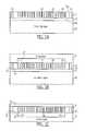
- FIGS. 1A-1Dillustrate methods of forming substrates having two-sided microstructures therein, according to embodiments of the invention.
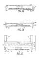
- FIGS. 2A-2Cillustrate methods of forming substrates having two-sided microstructures therein, according to embodiments of the invention.
- first, second, third etc.may be used herein to describe various elements, components, regions, layers and/or sections, these elements, components, regions, layers and/or sections should not be limited by these terms. These terms are only used to distinguish one element, component, region, layer or section from another region, layer or section. Thus, a first element, component, region, layer or section discussed below could be termed a second element, component, region, layer or section without departing from the teachings of the present invention.
- spatially relative termssuch as “beneath,” “below,” “lower,” “above,” “upper” and the like, may be used herein for ease of description to describe one element or feature's relationship to another element(s) or feature(s) as illustrated in the figures. It will be understood that the spatially relative terms are intended to encompass different orientations of the device in use or operation in addition to the orientation depicted in the figures. For example, if the device in the figures is turned over, elements described as “below” or “beneath” other elements or features would then be oriented “above” the other elements or features. Thus, the term “below” can encompass both an orientation of above and below. The device may be otherwise oriented (rotated 90 degrees or at other orientations) and the spatially relative descriptors used herein interpreted accordingly.
- Embodiments of the present inventionare described herein with reference to cross-section and perspective illustrations that are schematic illustrations of idealized embodiments (and intermediate structures) of the present invention. As such, variations from the shapes of the illustrations as a result, for example, of manufacturing techniques and/or tolerances, are to be expected. Thus, embodiments of the present invention should not be construed as limited to the particular shapes of regions illustrated herein but are to include deviations in shapes that result, for example, from manufacturing. For example, a sharp angle may be somewhat rounded due to manufacturing techniques/tolerances.
- a method of forming a substrate having two-sided microstructures thereinincludes forming device structures 16 and alignment keys 18 in a first surface 20 a of a semiconductor-on-insulator substrate (SOI).
- SOI substrateis illustrated as containing a handling layer 10 (e.g., semiconductor wafer), an electrically insulating layer 12 (e.g., silicon dioxide layer) on the handling layer 10 , and a semiconductor device layer 14 on the electrically insulating layer 12 .
- a handling layer 10e.g., semiconductor wafer
- an electrically insulating layer 12e.g., silicon dioxide layer
- the device structures 16which extend only partially through the semiconductor device layer 14
- the alignment keys 18which may extend entirely through the semiconductor device layer 14 to a second surface 20 b of the semiconductor device layer 14
- a photoresist layer(not shown) may be deposited on the first surface 20 a of the semiconductor device layer 14 after the device structures 16 and intermediate alignment marks (not shown) are concurrently etched. This photoresist layer may then be patterned to expose only the intermediate alignment marks and support further selective etching of the bottoms of the intermediate alignment marks until the second surface 20 b is reached and the alignment marks 18 are fully defined.
- a capping layer 22 having a recess 24 thereinis bonded to the first surface 20 a of the semiconductor device layer 14 .
- the dimensions of the recess 24may be sufficient to provide a sealed cavity to the device structures 16 , which may be microelectromechanical resonator structures. Examples of microelectromechanical resonator structures that may be used in embodiments of the invention are disclosed in U.S. Pat. Nos. 7,834,524 and 7,888,843 and U.S. Patent Pub. Nos. 2010/0194241 and 2010/0319185, the disclosures of which are hereby incorporated herein by reference.
- the capping layer 22may be a semiconductor (e.g., silicon) wafer having a preformed recess(es) therein.
- FIGS. 1C-1Dillustrate the exposure of the alignment marks 18 at the second surface 20 b of the semiconductor device layer 14 , which is caused by the removal of the handling layer 10 and the electrically insulating layer 12 using conventional techniques. These techniques include wafer grinding, deep reactive ion etching (DRIE) and chemical-mechanical polishing (CMP) for the handling layer 10 and dry or wet etching (e.g., wet HF solution) for the electrically insulating layer 12 .
- the second surface 20 b of the semiconductor device layer 14may then be covered with a photoresist layer 30 , which is subsequently patterned using a photolithographically-defined exposure process.
- This exposure processmay including the use of a mask 40 and photolithographic processing equipment.
- This processing equipmentcan contain lens elements 44 that enable high precision alignment between alignment patterns 42 on the mask 40 and the alignment marks 18 exposed at the second surface 20 b of the semiconductor device layer 14 .
- an additional method of forming a substrate having two-sided microstructures thereinincludes forming device structures 16 and intermediate alignment keys 18 a in a first surface 20 a of a substrate, which contains a semiconductor device layer 14 .
- the device structures 16 and the deeper intermediate alignment keys 18 aextend partially through the semiconductor device layer 14 , as illustrated by FIG. 2A .
- FIG. 2Billustrates the thermal oxidation of the second surface 20 b of the substrate, which results in the formation of an optically transparent thermal oxide layer 28 .
- This layer 28is made sufficiently thick to thereby recess the second surface 20 b of the semiconductor device layer 14 to a sufficient degree to encounter bottoms of the alignment keys 18 .
- FIG. 1illustrates the thermal oxide layer 28 .
- the alignment patterns 42 on the mask 40can then be aligned to the alignment keys 18 using conventional techniques.
- the thermal oxide layer 28is typically formed to a thickness of a few microns in order to maintain a high degree of optical transparency.
Landscapes
- Engineering & Computer Science (AREA)
- Physics & Mathematics (AREA)
- Geometry (AREA)
- Manufacturing & Machinery (AREA)
- Microelectronics & Electronic Packaging (AREA)
- Micromachines (AREA)
Abstract
Description
Claims (8)
Priority Applications (1)
| Application Number | Priority Date | Filing Date | Title |
|---|---|---|---|
| US13/034,004US8283256B1 (en) | 2011-02-24 | 2011-02-24 | Methods of forming microdevice substrates using double-sided alignment techniques |
Applications Claiming Priority (1)
| Application Number | Priority Date | Filing Date | Title |
|---|---|---|---|
| US13/034,004US8283256B1 (en) | 2011-02-24 | 2011-02-24 | Methods of forming microdevice substrates using double-sided alignment techniques |
Publications (1)
| Publication Number | Publication Date |
|---|---|
| US8283256B1true US8283256B1 (en) | 2012-10-09 |
Family
ID=46964211
Family Applications (1)
| Application Number | Title | Priority Date | Filing Date |
|---|---|---|---|
| US13/034,004Active2031-03-04US8283256B1 (en) | 2011-02-24 | 2011-02-24 | Methods of forming microdevice substrates using double-sided alignment techniques |
Country Status (1)
| Country | Link |
|---|---|
| US (1) | US8283256B1 (en) |
Cited By (5)
| Publication number | Priority date | Publication date | Assignee | Title |
|---|---|---|---|---|
| US9810581B1 (en) | 2014-07-28 | 2017-11-07 | MP High Tech Solutions Pty Ltd | Micromechanical device for electromagnetic radiation sensing |
| US9851256B2 (en) | 2014-06-26 | 2017-12-26 | MP High Tech Solutions Pty Ltd | Apparatus and method for electromagnetic radiation sensing |
| US9857229B1 (en)* | 2015-06-24 | 2018-01-02 | MP High Tech Solutions Pty Ltd | Fabrication method for micromechanical sensors |
| CN112558437A (en)* | 2020-12-18 | 2021-03-26 | 中国科学院光电技术研究所 | Processing method of double-sided few-layer super-structured surface device |
| WO2021134688A1 (en)* | 2019-12-31 | 2021-07-08 | 瑞声声学科技(深圳)有限公司 | Method for producing mems drive |
Citations (6)
| Publication number | Priority date | Publication date | Assignee | Title |
|---|---|---|---|---|
| US5952694A (en)* | 1991-11-20 | 1999-09-14 | Canon Kabushiki Kaisha | Semiconductor device made using processing from both sides of a workpiece |
| US6225145B1 (en)* | 1998-09-07 | 2001-05-01 | Electronics And Telecommunications Research Institute | Method of fabricating vacuum micro-structure |
| US20050006502A1 (en) | 1999-03-02 | 2005-01-13 | Schultz Gary A. | Integrated monolithic microfabricated dispensing nozzle and liquid chromatography-electrospray system and method |
| US20070230721A1 (en)* | 2006-01-23 | 2007-10-04 | White Robert D | Trapped fluid microsystems for acoustic sensing |
| US20080157283A1 (en)* | 2006-10-09 | 2008-07-03 | Mehrdad Moslehi | Template for three-dimensional thin-film solar cell manufacturing and methods of use |
| US20110140216A1 (en)* | 2009-12-16 | 2011-06-16 | Oakland University | Method of wafer-level fabrication of MEMS devices |
- 2011
- 2011-02-24USUS13/034,004patent/US8283256B1/enactiveActive
Patent Citations (6)
| Publication number | Priority date | Publication date | Assignee | Title |
|---|---|---|---|---|
| US5952694A (en)* | 1991-11-20 | 1999-09-14 | Canon Kabushiki Kaisha | Semiconductor device made using processing from both sides of a workpiece |
| US6225145B1 (en)* | 1998-09-07 | 2001-05-01 | Electronics And Telecommunications Research Institute | Method of fabricating vacuum micro-structure |
| US20050006502A1 (en) | 1999-03-02 | 2005-01-13 | Schultz Gary A. | Integrated monolithic microfabricated dispensing nozzle and liquid chromatography-electrospray system and method |
| US20070230721A1 (en)* | 2006-01-23 | 2007-10-04 | White Robert D | Trapped fluid microsystems for acoustic sensing |
| US20080157283A1 (en)* | 2006-10-09 | 2008-07-03 | Mehrdad Moslehi | Template for three-dimensional thin-film solar cell manufacturing and methods of use |
| US20110140216A1 (en)* | 2009-12-16 | 2011-06-16 | Oakland University | Method of wafer-level fabrication of MEMS devices |
Non-Patent Citations (1)
| Title |
|---|
| Gruber, M. et al., "Precise and Simple Optical Alignment Method for Double-Sided Lithography" Applied Optics, vol. 40, Issue 28, Oct. 1, 2001, pp. 5052-5055; doi:10.1364/AO.40.005052. |
Cited By (9)
| Publication number | Priority date | Publication date | Assignee | Title |
|---|---|---|---|---|
| US9851256B2 (en) | 2014-06-26 | 2017-12-26 | MP High Tech Solutions Pty Ltd | Apparatus and method for electromagnetic radiation sensing |
| US10422698B2 (en) | 2014-06-26 | 2019-09-24 | Mp High Tech Solutions Pty Ltd. | Apparatus and method for electromagnetic radiation sensing |
| US9810581B1 (en) | 2014-07-28 | 2017-11-07 | MP High Tech Solutions Pty Ltd | Micromechanical device for electromagnetic radiation sensing |
| US10585002B2 (en) | 2014-07-28 | 2020-03-10 | MP High Tech Solutions Pty Ltd | Micromechanical device for electromagnetic radiation sensing |
| US9857229B1 (en)* | 2015-06-24 | 2018-01-02 | MP High Tech Solutions Pty Ltd | Fabrication method for micromechanical sensors |
| US10107691B2 (en) | 2015-06-24 | 2018-10-23 | Mp High Tech Solutions Pty Ltd. | Fabrication method for micromechanical sensors |
| WO2021134688A1 (en)* | 2019-12-31 | 2021-07-08 | 瑞声声学科技(深圳)有限公司 | Method for producing mems drive |
| CN112558437A (en)* | 2020-12-18 | 2021-03-26 | 中国科学院光电技术研究所 | Processing method of double-sided few-layer super-structured surface device |
| CN112558437B (en)* | 2020-12-18 | 2023-03-31 | 中国科学院光电技术研究所 | Processing method of double-sided few-layer super-structured surface device |
Similar Documents
| Publication | Publication Date | Title |
|---|---|---|
| US6458494B2 (en) | Etching method | |
| US9938138B2 (en) | MEMS device structure with a capping structure | |
| US8283256B1 (en) | Methods of forming microdevice substrates using double-sided alignment techniques | |
| US9412620B2 (en) | Three-dimensional integrated circuit device fabrication including wafer scale membrane | |
| EP2019081B1 (en) | Boron doped shell for MEMS device | |
| EP2493809A1 (en) | Structure manufacturing method and liquid discharge head substrate manufacturing method | |
| WO2009077538A2 (en) | Process of assembly with buried marks | |
| JP2008030189A (en) | Silicone-on-metal for mems device | |
| US7745308B2 (en) | Method of fabricating micro-vertical structure | |
| TWI271800B (en) | Manufacturing method of semiconductor structure | |
| KR100817813B1 (en) | A method for fabricating a micro structures with multi differential gap on silicon substrate | |
| CN102285636B (en) | Wet etching preparation processes for polygonal section silicon beam | |
| US9312227B2 (en) | Method of joining semiconductor substrate | |
| EP3732516B1 (en) | Techniques for fabricating waveguide facets and die separation | |
| US7759256B2 (en) | Micro-electro-mechanical system device and method for making same | |
| US20130224958A1 (en) | Through hole forming method | |
| US20070269959A1 (en) | Method of aligning mask layers to buried features | |
| EP2133307A2 (en) | Manufacturing method of a three-dimensional microstructure | |
| JP2000088686A (en) | Pedestal for semiconductor pressure sensor and its manufacture | |
| JP2005028487A (en) | Micro device and its manufacturing method | |
| KR100613604B1 (en) | Floating Structure Formation Method Using SOI Wafer | |
| CN117747533A (en) | Method for manufacturing substrate | |
| US20060104583A1 (en) | Method of fabricating ridge type waveguide integrated semiconductor optical device | |
| KR20210065196A (en) | Nano-pore flow cells and manufacturing methods | |
| JP2004347773A (en) | Micro device and method of manufacturing the same |
Legal Events
| Date | Code | Title | Description |
|---|---|---|---|
| AS | Assignment | Owner name:INTEGRATED DEVICE TECHNOLOGY, INC., CALIFORNIA Free format text:ASSIGNMENT OF ASSIGNORS INTEREST;ASSIGNORS:PAN, WANLING;BHUGRA, HARMEET;REEL/FRAME:025873/0189 Effective date:20110223 | |
| FEPP | Fee payment procedure | Free format text:PAYOR NUMBER ASSIGNED (ORIGINAL EVENT CODE: ASPN); ENTITY STATUS OF PATENT OWNER: LARGE ENTITY | |
| STCF | Information on status: patent grant | Free format text:PATENTED CASE | |
| FPAY | Fee payment | Year of fee payment:4 | |
| AS | Assignment | Owner name:JPMORGAN CHASE BANK, N.A., AS COLLATERAL AGENT, NE Free format text:SECURITY AGREEMENT;ASSIGNORS:INTEGRATED DEVICE TECHNOLOGY, INC.;GIGPEAK, INC.;MAGNUM SEMICONDUCTOR, INC.;AND OTHERS;REEL/FRAME:042166/0431 Effective date:20170404 Owner name:JPMORGAN CHASE BANK, N.A., AS COLLATERAL AGENT, NEW YORK Free format text:SECURITY AGREEMENT;ASSIGNORS:INTEGRATED DEVICE TECHNOLOGY, INC.;GIGPEAK, INC.;MAGNUM SEMICONDUCTOR, INC.;AND OTHERS;REEL/FRAME:042166/0431 Effective date:20170404 | |
| AS | Assignment | Owner name:GIGPEAK, INC., CALIFORNIA Free format text:RELEASE BY SECURED PARTY;ASSIGNOR:JPMORGAN CHASE BANK, N.A.;REEL/FRAME:048746/0001 Effective date:20190329 Owner name:INTEGRATED DEVICE TECHNOLOGY, INC., CALIFORNIA Free format text:RELEASE BY SECURED PARTY;ASSIGNOR:JPMORGAN CHASE BANK, N.A.;REEL/FRAME:048746/0001 Effective date:20190329 Owner name:MAGNUM SEMICONDUCTOR, INC., CALIFORNIA Free format text:RELEASE BY SECURED PARTY;ASSIGNOR:JPMORGAN CHASE BANK, N.A.;REEL/FRAME:048746/0001 Effective date:20190329 Owner name:CHIPX, INCORPORATED, CALIFORNIA Free format text:RELEASE BY SECURED PARTY;ASSIGNOR:JPMORGAN CHASE BANK, N.A.;REEL/FRAME:048746/0001 Effective date:20190329 Owner name:ENDWAVE CORPORATION, CALIFORNIA Free format text:RELEASE BY SECURED PARTY;ASSIGNOR:JPMORGAN CHASE BANK, N.A.;REEL/FRAME:048746/0001 Effective date:20190329 | |
| MAFP | Maintenance fee payment | Free format text:PAYMENT OF MAINTENANCE FEE, 8TH YEAR, LARGE ENTITY (ORIGINAL EVENT CODE: M1552); ENTITY STATUS OF PATENT OWNER: LARGE ENTITY Year of fee payment:8 | |
| MAFP | Maintenance fee payment | Free format text:PAYMENT OF MAINTENANCE FEE, 12TH YEAR, LARGE ENTITY (ORIGINAL EVENT CODE: M1553); ENTITY STATUS OF PATENT OWNER: LARGE ENTITY Year of fee payment:12 |