US8281052B2 - Dynamically setting burst length of double data rate memory device by applying signal to at least one external pin during a read or write transaction - Google Patents
Dynamically setting burst length of double data rate memory device by applying signal to at least one external pin during a read or write transactionDownload PDFInfo
- Publication number
- US8281052B2 US8281052B2US13/442,228US201213442228AUS8281052B2US 8281052 B2US8281052 B2US 8281052B2US 201213442228 AUS201213442228 AUS 201213442228AUS 8281052 B2US8281052 B2US 8281052B2
- Authority
- US
- United States
- Prior art keywords
- data rate
- memory device
- double data
- burst type
- burst
- Prior art date
- Legal status (The legal status is an assumption and is not a legal conclusion. Google has not performed a legal analysis and makes no representation as to the accuracy of the status listed.)
- Expired - Fee Related
Links
Images


Classifications
- G—PHYSICS
- G11—INFORMATION STORAGE
- G11C—STATIC STORES
- G11C7/00—Arrangements for writing information into, or reading information out from, a digital store
- G11C7/10—Input/output [I/O] data interface arrangements, e.g. I/O data control circuits, I/O data buffers
- G11C7/1015—Read-write modes for single port memories, i.e. having either a random port or a serial port
- G11C7/1045—Read-write mode select circuits
- G—PHYSICS
- G11—INFORMATION STORAGE
- G11C—STATIC STORES
- G11C7/00—Arrangements for writing information into, or reading information out from, a digital store
- G11C7/10—Input/output [I/O] data interface arrangements, e.g. I/O data control circuits, I/O data buffers
- G11C7/1015—Read-write modes for single port memories, i.e. having either a random port or a serial port
- G11C7/1018—Serial bit line access mode, e.g. using bit line address shift registers, bit line address counters, bit line burst counters
- G11C7/1027—Static column decode serial bit line access mode, i.e. using an enabled row address stroke pulse with its associated word line address and a sequence of enabled bit line addresses
- G—PHYSICS
- G11—INFORMATION STORAGE
- G11C—STATIC STORES
- G11C2207/00—Indexing scheme relating to arrangements for writing information into, or reading information out from, a digital store
- G11C2207/10—Aspects relating to interfaces of memory device to external buses
- G11C2207/105—Aspects related to pads, pins or terminals
Definitions
- the present inventionrelates to a method and apparatus which permits modification of the burst length of data in a memory device.
- a burst modeis known to be used in some memory devices to increase the speed of reading and writing data from and to the memory. Burst mode operation allows reads or writes from or to consecutive memory core locations at high speeds.
- a memory storage deviceuses one clock cycle to activate a row, giving the row address, and another clock cycle for column addressing. The READ or WRITE command is given with the column address on separate command lines.
- datais transferred from or to a memory device.
- a memory deviceFor example, 4 eight bit data bytes being read from or written to a DDR SDRAM requires one clock cycle to decode each of the four column addresses.
- the first column addressis issued with the READ or WRITE command with the subsequent column address being decoded internally on the DRAM device freeing up the command bus for other uses.
- a burst mode operationprovides relatively high data transfer rates and significantly reduces the latency involved in a memory transfer.
- the burst modeis generally controlled by setting one or more bits in a mode register provided within a memory device.
- data within the mode register 100controls a variety of different chip functions.
- Bits 13 and 14 of mode register 100are used to select between a base mode register and an extended mode register; bits 7 through 12 of mode register 100 determine the operating mode of the memory device; bits 4 - 6 of mode register 100 determine the column address strobe (“CAS”) latency; bit 3 of mode register 100 determines whether the burst type is sequential or interleaved; and, bits 0 - 2 of mode register 100 determine the burst length.
- CAScolumn address strobe
- the burst lengthdetermines the maximum number of consecutive column locations that can be accessed for a given READ or WRITE command without the need to use clock cycles to transfer subsequent intervening column addresses. As shown in tables 110 and 120 , burst lengths of 2, 4 or 8 bytes can be selected for each of the sequential and interleaved burst types which is set by bit position 3 .
- Mode register 100is programmed by a CPU or memory controller using a MODE REGISTER SET command and retains the set information until it is programmed again, or the memory device loses power.
- the mode registermust be programmed while all memory cores are idle and no data bursts are in progress, and the memory controller or CPU must wait a specified time before initiating a memory access operation subsequent to programming.
- a memory device which allows dynamic programming of burst lengthwould be desirable and would permit faster adjustment of the burst length.
- the present inventionmitigates the problems associated with current DRAM devices and provides a unique method and system of allowing a user to dynamically define burst length.
- control pins provided on a memory storage deviceare used to set burst length.
- a control pin on the memory storage devicecan be used to determine the burst type. Using control pins to set burst length and type allows the burst length to be set while the memory cores are in use and without waiting after changing the burst length and/or type before initiating a memory access operation.
- the address pins that are not used during column addressingare used for setting the burst length and/or burst type.
- This embodimentalso allows the burst length and/or burst type to be set while the memory cores are in use and without waiting after changing the burst length and/or type before initiating a memory access operation.
- the burst lengthdoes not necessarily have to be set on active commands, READs or WRITEs.
- FIG. 1is an illustration of a conventional memory device mode register and its contents
- FIG. 2is an illustration of the layout of control pins in a preferred embodiment of the present invention
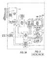
- FIG. 3is an illustration of a block diagram of a 256 Mx16 DDR SDRAM implementing the present invention.
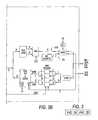
- FIG. 4is an illustration of a burst length latch in a preferred embodiment of the present invention.
- FIG. 5is an illustration of a burst type latch in a preferred embodiment of the present invention.
- FIG. 6is an illustration of a column address counter/latch in an exemplary embodiment of the present invention.
- FIG. 7illustrates a processor system which includes electronic devices containing the invention.
- external pins provided on a memory storage deviceare used to dynamically set the burst length or hard set the burst length.
- An exemplary memory device 200which may employ the invention is shown in FIG. 2 , and is a 256 Mb double data rate synchronous DRAM (DDR SDRAM). As can be seen, memory device 200 has a plurality of control pins (for example, pins 21 , 22 , 23 , 24 are control pins). While the following description of a preferred embodiment of the present invention is described with reference to a 256 Mb DDR SDRAM, the present invention can be implemented with any memory storage device having external pins.
- DDR SDRAMdouble data rate synchronous DRAM
- Memory storage device 200can be configured to use a single external pin to toggle between two possible burst lengths or a plurality of external pins if a larger number of burst lengths is desired.
- NCnot connected
- the present inventioncan be easily incorporated into most chip designs.
- One or more of the NC pinscan be used as burst length toggle pins. For example, if two possible burst lengths are desired, pin 17 of memory storage device 200 , which is labeled NC in FIG. 2 , can be used. If the two possible burst lengths are 4 bytes and 8 bytes, then when pin 17 is high, the burst length is e.g.
- NC pin 25can also be used as up to four burst lengths can be programmed with two control pins. Although the description discusses several different burst lengths, the number of dynamically defined burst lengths is determined based on the number of available external pins.
- FIG. 3is a block diagram of the FIG. 2 256 Mx16 DDR SDRAM.
- Control logic 310receives a data signal on the burst length input pin (e.g. external pin 17 ) as an input.
- a data signal on the burst length input pine.g. external pin 17
- One or more external pinscan be used to input burst length data.
- a command decode circuit 312which is part of the memory device control logic 310 , determines what the burst length is based on the data signals applied to the external burst control pin(s). For example, if the external burst pin is a single pin 17 (i.e.
- the command decodedetermines if the voltage on pin 17 is set to V cc indicating a first burst length or V, indicating a second burst length.
- the status of the one or more burst length pinssets appropriate internal burst codes ( FIG. 4 , decode circuits 75 , 77 ) within the command and decode circuit 312 .
- the burst lengthwould previously be output from mode register 100 ( FIG. 1 ) to other circuits within control logic 310 ( FIG. 2 ) to set burst length, in the present invention, it is output to the other circuits from one or more decode circuits or data latches 75 , 77 ( FIG. 4 ) within command decode circuit 312 which now contains this data.
- the burst length datais used by the control logic 310 to set burst length. Accordingly, nothing outside of the control logic 310 needs to be changed to implement the present invention, and very little change within control logic 310 is required.
- the burst lengthcan be controlled dynamically from the exterior of the memory device 100 .
- the burst lengthalso can be changed simultaneously with a READ or WRITE command.
- the burst typecan also be set using external control pins. This allows the burst type to also be set dynamically. As with using the external control pins to adjust burst length, using the external control pins to determine the burst type can be easily incorporated into most existing memory storage device designs by using another one of the NC pins. For example, referring to FIG. 2 , external pin 53 could be used to determine burst type of the memory device 200 . If burst type pin 53 is e.g. high, the burst type is interleaved; if burst type pin 53 is e.g. low, the burst type is sequential.
- a decode circuit 79within the column decode and burst counter circuit 312 receives a data signal applied to external pin 53 and the output of this circuit 79 goes to the same circuitry within the control logic 312 which processes burst type data previously set in the mode register 100 .
- controlling burst type with an external control pinonly requires a small internal change within control logic 310 .
- Another exemplary embodiment of the present inventionuses the address pins to set burst length and/or burst type.
- thirteen external pinse.g. A 0 -A 12
- address register 320for addressing.
- Both row and column addressesuse the same 13 pins.
- 10A 0 , . . . , A 9
- the remaining three pinsA 10 . . . A 12
- burst length datais applied to one or more of address pins A 10 . . . A 12 .
- FIG. 6shows two such address lines (A 10 , A 11 ) being used for this purpose.
- a decode circuit 81decodes this data and supplies the burst length information to the column address counter/latch 330 ( FIG. 3 ). If less than all of the unused address lines are required for setting burst length, any remaining lines, e.g. A 12 in FIG. 6 , can be used to set burst type decode circuit 77 ( FIG. 5 ).
- FIG. 6shows a decoder 81 for the burst length signal(s) which is external to the column address counter/latch 330 , decoder 81 may also be incorporated within the column address counter/latch 330 .
- the mode register for a memory device implementing embodiments of the present inventiondoes not require the bit positions A 0 -A 2 illustrated in mode register 100 for setting burst length and/or bit position A 3 for setting burst type and can therefore be made shorter in length, or the unused bit positions may be used for other functions.
- the inventionmay be used in many types of memory devices in addition to the DDR SDRAM memory device illustrated in FIGS. 2 and 3 .
- FIG. 7shows a processor system, such as, for example, a computer system in which the invention may be used.
- the processor systemgenerally comprises a central processing unit (CPU) 710 , for example, a microprocessor, that communicates with one or more input/output (I/O) devices 740 , 750 over a bus 770 .
- the system 700also includes random access memory (RAM) 760 , a read only memory (ROM) 780 and, in the case of a computer system may include a permanent data storage device 708 and peripheral devices such as a floppy disk drive 720 and a compact disk (CD) ROM drive 730 which also communicates with CPU 710 over the bus 770 .
- RAMrandom access memory
- ROMread only memory
- the random access memory (RAM) 760may incorporate external pin control of burst length and/or burst type in accordance with the invention.
- one or more of memory devices 760 , 780may be fabricated as an integral part with CPU 710 . While FIG. 7 represents one processor system architecture, many others are also possible.
Landscapes
- Dram (AREA)
Abstract
Description
This application is a continuation application of U.S. patent application Ser. No. 13/212,731, filed Aug. 18, 2011, which is scheduled to issue as U.S. Pat. No. 8,156,262 on Apr. 10, 2012, which is a continuation application of U.S. patent application Ser. No. 12/503,097, filed Jul. 15, 2009, which issued as U.S. Pat. No. 8,019,913 on Sep. 13, 2011, which is a continuation of U.S. application Ser. No. 11/296,359, filed Dec. 8, 2005, which issued as U.S. Pat. No. 7,603,493 on Oct. 13, 2009, which is a divisional of U.S. patent application Ser. No. 10/191,290 filed Jul. 10, 2002, which issued as U.S. Pat. No. 7,149,824 on Dec. 12, 2006, the disclosures of which are hereby incorporated herein by reference.
The present invention relates to a method and apparatus which permits modification of the burst length of data in a memory device.
A burst mode is known to be used in some memory devices to increase the speed of reading and writing data from and to the memory. Burst mode operation allows reads or writes from or to consecutive memory core locations at high speeds. When a burst mode is not implemented, a memory storage device uses one clock cycle to activate a row, giving the row address, and another clock cycle for column addressing. The READ or WRITE command is given with the column address on separate command lines.
In the clock cycle(s) following the addressing/command cycles, data is transferred from or to a memory device. For example, 4 eight bit data bytes being read from or written to a DDR SDRAM requires one clock cycle to decode each of the four column addresses. The first column address is issued with the READ or WRITE command with the subsequent column address being decoded internally on the DRAM device freeing up the command bus for other uses.
In addition, by eliminating column decoding time, the command bus is free to reduce latency during back intervening. Accordingly, a burst mode operation provides relatively high data transfer rates and significantly reduces the latency involved in a memory transfer.
The burst mode is generally controlled by setting one or more bits in a mode register provided within a memory device. As shown inFIG. 1 , which depicts one exemplary memory device mode register, data within themode register 100 controls a variety of different chip functions.Bits mode register 100 are used to select between a base mode register and an extended mode register;bits 7 through12 ofmode register 100 determine the operating mode of the memory device; bits4-6 ofmode register 100 determine the column address strobe (“CAS”) latency;bit 3 ofmode register 100 determines whether the burst type is sequential or interleaved; and, bits0-2 ofmode register 100 determine the burst length.
The burst length determines the maximum number of consecutive column locations that can be accessed for a given READ or WRITE command without the need to use clock cycles to transfer subsequent intervening column addresses. As shown in tables110 and120, burst lengths of 2, 4 or 8 bytes can be selected for each of the sequential and interleaved burst types which is set bybit position 3.
A memory device which allows dynamic programming of burst length would be desirable and would permit faster adjustment of the burst length.
The present invention mitigates the problems associated with current DRAM devices and provides a unique method and system of allowing a user to dynamically define burst length.
In accordance with an exemplary embodiment of the present invention, control pins provided on a memory storage device are used to set burst length. In addition, a control pin on the memory storage device can be used to determine the burst type. Using control pins to set burst length and type allows the burst length to be set while the memory cores are in use and without waiting after changing the burst length and/or type before initiating a memory access operation.
In another exemplary embodiment of the present invention, the address pins that are not used during column addressing are used for setting the burst length and/or burst type. This embodiment also allows the burst length and/or burst type to be set while the memory cores are in use and without waiting after changing the burst length and/or type before initiating a memory access operation. The burst length does not necessarily have to be set on active commands, READs or WRITEs.
The above and other features and advantages of the invention will be more readily understood from the following detailed description of the invention which is provided in connection with the accompanying drawings.
In the following detailed description, reference is made to the accompanying drawings which form a part hereof, and in which is shown by way of illustration specific embodiments in which the invention may be practiced. These embodiments are described in sufficient detail to enable those skilled in the art to make and use the invention, and it is to be understood that structural changes may be made and equivalent structures substituted for those shown without departing from the spirit and scope of the present invention.
In accordance with an exemplary embodiment of the present invention, external pins provided on a memory storage device are used to dynamically set the burst length or hard set the burst length. Anexemplary memory device 200 which may employ the invention is shown inFIG. 2 , and is a 256 Mb double data rate synchronous DRAM (DDR SDRAM). As can be seen,memory device 200 has a plurality of control pins (for example,pins
Implementation of the present invention requires very little internal change to existing memory devices. Thus, where the burst length would previously be output from mode register100 (FIG. 1 ) to other circuits within control logic310 (FIG. 2 ) to set burst length, in the present invention, it is output to the other circuits from one or more decode circuits or data latches75,77 (FIG. 4 ) withincommand decode circuit 312 which now contains this data. In both the conventional memory device ofFIG. 2 and one in accordance with the present invention, the burst length data is used by thecontrol logic 310 to set burst length. Accordingly, nothing outside of thecontrol logic 310 needs to be changed to implement the present invention, and very little change withincontrol logic 310 is required.
By using external control pins to control the burst length instead of themode register 100, the burst length can be controlled dynamically from the exterior of thememory device 100. The burst length also can be changed simultaneously with a READ or WRITE command.
In addition to using the external control pins to determine the burst length, the burst type can also be set using external control pins. This allows the burst type to also be set dynamically. As with using the external control pins to adjust burst length, using the external control pins to determine the burst type can be easily incorporated into most existing memory storage device designs by using another one of the NC pins. For example, referring toFIG. 2 ,external pin 53 could be used to determine burst type of thememory device 200. If bursttype pin 53 is e.g. high, the burst type is interleaved; ifburst type pin 53 is e.g. low, the burst type is sequential.
The same type of modifications necessary to change control of the burst length frommode register 100 to theexternal pin 17 are necessary to change control of the burst type frommode register 100 toexternal pin 53. Thus, a decode circuit79 (FIG. 5 ) within the column decode and burstcounter circuit 312 receives a data signal applied toexternal pin 53 and the output of thiscircuit 79 goes to the same circuitry within thecontrol logic 312 which processes burst type data previously set in themode register 100. Thus, controlling burst type with an external control pin only requires a small internal change withincontrol logic 310.
Another exemplary embodiment of the present invention uses the address pins to set burst length and/or burst type. As shown inFIG. 3 , thirteen external pins (e.g. A0-A12) are input intoaddress register 320 for addressing. Both row and column addresses use the same 13 pins. During column addressing, however, only 10 (A0, . . . , A9) of the 13 pins are needed. The remaining three pins (A10 . . . A12) can be used to determine burst length and/or burst type.
In this embodiment burst length data is applied to one or more of address pins A10 . . . A12.FIG. 6 shows two such address lines (A10, A11) being used for this purpose. A decode circuit81 decodes this data and supplies the burst length information to the column address counter/latch330 (FIG. 3 ). If less than all of the unused address lines are required for setting burst length, any remaining lines, e.g. A12 inFIG. 6 , can be used to set burst type decode circuit77 (FIG. 5 ).
It should be noted that althoughFIG. 6 shows a decoder81 for the burst length signal(s) which is external to the column address counter/latch 330, decoder81 may also be incorporated within the column address counter/latch 330.
The mode register for a memory device implementing embodiments of the present invention does not require the bit positions A0-A2 illustrated inmode register 100 for setting burst length and/or bit position A3 for setting burst type and can therefore be made shorter in length, or the unused bit positions may be used for other functions.
The invention may be used in many types of memory devices in addition to the DDR SDRAM memory device illustrated inFIGS. 2 and 3 .
While the invention has been described with reference to an exemplary embodiments various additions, deletions, substitutions, or other modifications may be made without departing from the spirit or scope of the invention. Accordingly, the invention is not to be considered as limited by the foregoing description, but is only limited by the scope of the appended claims.
Although the invention herein has been described with reference to particular embodiments, it is to be understood that these embodiments are merely illustrative of the principles and applications of the present invention. It is therefore to be understood that numerous modifications may be made to the illustrative embodiments and that other arrangements may be devised without departing from the spirit and scope of the present invention as defined by the appended claims.
Claims (10)
1. A microprocessor system, comprising:
a central processing unit in communication with a bus;
a random access memory in communication with the bus and the central processing unit, the random access memory having a double data rate memory device having separate groups of external pins adapted to receive addressing, data, and control information; and
a memory controller adapted to set a burst type of the double data rate memory to interleaved or sequential by sending a signal through one of the external pins of the double data rate memory device, such that when a read command is sent by the controller, depending on the burst type set, the double data rate memory device returns interleaved or sequentially output data to the memory controller.
2. The system ofclaim 1 , wherein the burst type is set proximate to when a read command is received at the double data rate memory device.
3. The system ofclaim 1 , wherein the external pin to which the burst type setting signal is sent by the memory controller is an address pin.
4. The system ofclaim 3 , wherein the address pin is A3.
5. The system ofclaim 1 , wherein if a logic value corresponding to the signal sent to the external pin is high, the burst type is set to interleaved, and if the logic value corresponding to the signal sent to the external pin is low, the burst type is set to sequential.
6. A microprocessor system, comprising:
a central processing unit in communication with a bus;
a random access memory integrated with the microprocessor, the random access memory having a double data rate memory device having separate groups of external pins adapted to receive addressing, data, and control information; and
a memory controller adapted to set a burst type of the double data rate memory to interleaved or sequential by sending a signal through one of the external pins of the double data rate memory device, such that when a read command is sent by the controller, depending on the burst type set, the double data rate memory device returns interleaved or sequentially output data to the memory controller.
7. The system ofclaim 6 , wherein the burst type is set proximate to when a read command is received at the double data rate memory device.
8. The system ofclaim 7 , wherein the external pin to which the burst type setting signal is sent by the memory controller is an address pin.
9. The system ofclaim 8 , wherein the address pin is A3.
10. The system ofclaim 6 , wherein if a logic value corresponding to the signal sent to the external pin is high, the burst type is set to interleaved, and if the logic value corresponding to the signal sent to the external pin is low, the burst type is set to sequential.
Priority Applications (1)
| Application Number | Priority Date | Filing Date | Title |
|---|---|---|---|
| US13/442,228US8281052B2 (en) | 2002-07-10 | 2012-04-09 | Dynamically setting burst length of double data rate memory device by applying signal to at least one external pin during a read or write transaction |
Applications Claiming Priority (5)
| Application Number | Priority Date | Filing Date | Title |
|---|---|---|---|
| US10/191,290US7149824B2 (en) | 2002-07-10 | 2002-07-10 | Dynamically setting burst length of memory device by applying signal to at least one external pin during a read or write transaction |
| US11/296,359US7603493B2 (en) | 2002-07-10 | 2005-12-08 | Dynamically setting burst length of memory device by applying signal to at least one external pin during a read or write transaction |
| US12/503,097US8019913B2 (en) | 2002-07-10 | 2009-07-15 | Dynamically setting burst length of double data rate memory device by applying signal to at least one external pin during a read or write transaction |
| US13/212,731US8156262B2 (en) | 2002-07-10 | 2011-08-18 | Dynamically setting burst length of double data rate memory device by applying signal to at least one external pin during a read or write transaction |
| US13/442,228US8281052B2 (en) | 2002-07-10 | 2012-04-09 | Dynamically setting burst length of double data rate memory device by applying signal to at least one external pin during a read or write transaction |
Related Parent Applications (1)
| Application Number | Title | Priority Date | Filing Date |
|---|---|---|---|
| US13/212,731ContinuationUS8156262B2 (en) | 2002-07-10 | 2011-08-18 | Dynamically setting burst length of double data rate memory device by applying signal to at least one external pin during a read or write transaction |
Publications (2)
| Publication Number | Publication Date |
|---|---|
| US20120198144A1 US20120198144A1 (en) | 2012-08-02 |
| US8281052B2true US8281052B2 (en) | 2012-10-02 |
Family
ID=30114147
Family Applications (6)
| Application Number | Title | Priority Date | Filing Date |
|---|---|---|---|
| US10/191,290Expired - Fee RelatedUS7149824B2 (en) | 2002-07-10 | 2002-07-10 | Dynamically setting burst length of memory device by applying signal to at least one external pin during a read or write transaction |
| US11/296,359Expired - Fee RelatedUS7603493B2 (en) | 2002-07-10 | 2005-12-08 | Dynamically setting burst length of memory device by applying signal to at least one external pin during a read or write transaction |
| US12/503,097Expired - Fee RelatedUS8019913B2 (en) | 2002-07-10 | 2009-07-15 | Dynamically setting burst length of double data rate memory device by applying signal to at least one external pin during a read or write transaction |
| US12/543,584Expired - Fee RelatedUS7984207B2 (en) | 2002-07-10 | 2009-08-19 | Dynamically setting burst length of double data rate memory device by applying signal to at least one external pin during a read or write transaction |
| US13/212,731Expired - Fee RelatedUS8156262B2 (en) | 2002-07-10 | 2011-08-18 | Dynamically setting burst length of double data rate memory device by applying signal to at least one external pin during a read or write transaction |
| US13/442,228Expired - Fee RelatedUS8281052B2 (en) | 2002-07-10 | 2012-04-09 | Dynamically setting burst length of double data rate memory device by applying signal to at least one external pin during a read or write transaction |
Family Applications Before (5)
| Application Number | Title | Priority Date | Filing Date |
|---|---|---|---|
| US10/191,290Expired - Fee RelatedUS7149824B2 (en) | 2002-07-10 | 2002-07-10 | Dynamically setting burst length of memory device by applying signal to at least one external pin during a read or write transaction |
| US11/296,359Expired - Fee RelatedUS7603493B2 (en) | 2002-07-10 | 2005-12-08 | Dynamically setting burst length of memory device by applying signal to at least one external pin during a read or write transaction |
| US12/503,097Expired - Fee RelatedUS8019913B2 (en) | 2002-07-10 | 2009-07-15 | Dynamically setting burst length of double data rate memory device by applying signal to at least one external pin during a read or write transaction |
| US12/543,584Expired - Fee RelatedUS7984207B2 (en) | 2002-07-10 | 2009-08-19 | Dynamically setting burst length of double data rate memory device by applying signal to at least one external pin during a read or write transaction |
| US13/212,731Expired - Fee RelatedUS8156262B2 (en) | 2002-07-10 | 2011-08-18 | Dynamically setting burst length of double data rate memory device by applying signal to at least one external pin during a read or write transaction |
Country Status (1)
| Country | Link |
|---|---|
| US (6) | US7149824B2 (en) |
Families Citing this family (57)
| Publication number | Priority date | Publication date | Assignee | Title |
|---|---|---|---|---|
| US7191162B2 (en)* | 2003-10-21 | 2007-03-13 | Texas Instruments Incorporated | FIFO interface for flag-initiated DMA frame synchro-burst operation |
| US7328288B2 (en)* | 2003-12-11 | 2008-02-05 | Canon Kabushiki Kaisha | Relay apparatus for relaying communication from CPU to peripheral device |
| US20050268022A1 (en)* | 2004-05-26 | 2005-12-01 | Pelley Perry H | Cache line memory and method therefor |
| US7221613B2 (en) | 2004-05-26 | 2007-05-22 | Freescale Semiconductor, Inc. | Memory with serial input/output terminals for address and data and method therefor |
| US8111566B1 (en) | 2007-11-16 | 2012-02-07 | Google, Inc. | Optimal channel design for memory devices for providing a high-speed memory interface |
| US8077535B2 (en) | 2006-07-31 | 2011-12-13 | Google Inc. | Memory refresh apparatus and method |
| US7590796B2 (en) | 2006-07-31 | 2009-09-15 | Metaram, Inc. | System and method for power management in memory systems |
| US8041881B2 (en) | 2006-07-31 | 2011-10-18 | Google Inc. | Memory device with emulated characteristics |
| US20080082763A1 (en) | 2006-10-02 | 2008-04-03 | Metaram, Inc. | Apparatus and method for power management of memory circuits by a system or component thereof |
| US8081474B1 (en) | 2007-12-18 | 2011-12-20 | Google Inc. | Embossed heat spreader |
| US8438328B2 (en) | 2008-02-21 | 2013-05-07 | Google Inc. | Emulation of abstracted DIMMs using abstracted DRAMs |
| US7609567B2 (en) | 2005-06-24 | 2009-10-27 | Metaram, Inc. | System and method for simulating an aspect of a memory circuit |
| US8060774B2 (en) | 2005-06-24 | 2011-11-15 | Google Inc. | Memory systems and memory modules |
| US8055833B2 (en) | 2006-10-05 | 2011-11-08 | Google Inc. | System and method for increasing capacity, performance, and flexibility of flash storage |
| US8130560B1 (en) | 2006-11-13 | 2012-03-06 | Google Inc. | Multi-rank partial width memory modules |
| US8386722B1 (en) | 2008-06-23 | 2013-02-26 | Google Inc. | Stacked DIMM memory interface |
| US9171585B2 (en) | 2005-06-24 | 2015-10-27 | Google Inc. | Configurable memory circuit system and method |
| US10013371B2 (en) | 2005-06-24 | 2018-07-03 | Google Llc | Configurable memory circuit system and method |
| US8244971B2 (en) | 2006-07-31 | 2012-08-14 | Google Inc. | Memory circuit system and method |
| US8335894B1 (en) | 2008-07-25 | 2012-12-18 | Google Inc. | Configurable memory system with interface circuit |
| KR101377305B1 (en) | 2005-06-24 | 2014-03-25 | 구글 인코포레이티드 | An integrated memory core and memory interface circuit |
| US8090897B2 (en) | 2006-07-31 | 2012-01-03 | Google Inc. | System and method for simulating an aspect of a memory circuit |
| US9507739B2 (en) | 2005-06-24 | 2016-11-29 | Google Inc. | Configurable memory circuit system and method |
| US8359187B2 (en) | 2005-06-24 | 2013-01-22 | Google Inc. | Simulating a different number of memory circuit devices |
| US7580312B2 (en) | 2006-07-31 | 2009-08-25 | Metaram, Inc. | Power saving system and method for use with a plurality of memory circuits |
| US8327104B2 (en) | 2006-07-31 | 2012-12-04 | Google Inc. | Adjusting the timing of signals associated with a memory system |
| US8089795B2 (en) | 2006-02-09 | 2012-01-03 | Google Inc. | Memory module with memory stack and interface with enhanced capabilities |
| US8397013B1 (en) | 2006-10-05 | 2013-03-12 | Google Inc. | Hybrid memory module |
| US7392338B2 (en) | 2006-07-31 | 2008-06-24 | Metaram, Inc. | Interface circuit system and method for autonomously performing power management operations in conjunction with a plurality of memory circuits |
| US7386656B2 (en) | 2006-07-31 | 2008-06-10 | Metaram, Inc. | Interface circuit system and method for performing power management operations in conjunction with only a portion of a memory circuit |
| US20080028136A1 (en) | 2006-07-31 | 2008-01-31 | Schakel Keith R | Method and apparatus for refresh management of memory modules |
| US8796830B1 (en) | 2006-09-01 | 2014-08-05 | Google Inc. | Stackable low-profile lead frame package |
| US9542352B2 (en) | 2006-02-09 | 2017-01-10 | Google Inc. | System and method for reducing command scheduling constraints of memory circuits |
| WO2007028109A2 (en) | 2005-09-02 | 2007-03-08 | Metaram, Inc. | Methods and apparatus of stacking drams |
| US9632929B2 (en) | 2006-02-09 | 2017-04-25 | Google Inc. | Translating an address associated with a command communicated between a system and memory circuits |
| US7724589B2 (en) | 2006-07-31 | 2010-05-25 | Google Inc. | System and method for delaying a signal communicated from a system to at least one of a plurality of memory circuits |
| US20080301391A1 (en)* | 2007-06-01 | 2008-12-04 | Jong-Hoon Oh | Method and apparatus for modifying a burst length for semiconductor memory |
| US8209479B2 (en) | 2007-07-18 | 2012-06-26 | Google Inc. | Memory circuit system and method |
| US8080874B1 (en) | 2007-09-14 | 2011-12-20 | Google Inc. | Providing additional space between an integrated circuit and a circuit board for positioning a component therebetween |
| KR101443231B1 (en)* | 2007-11-27 | 2014-09-19 | 삼성전자주식회사 | Cache memory capable of adjusting burst length of write-back data in write-back operation |
| DE202010017690U1 (en) | 2009-06-09 | 2012-05-29 | Google, Inc. | Programming dimming terminating resistor values |
| JP2011175563A (en) | 2010-02-25 | 2011-09-08 | Elpida Memory Inc | Data processing system and control method thereof |
| KR101796116B1 (en) | 2010-10-20 | 2017-11-10 | 삼성전자 주식회사 | Semiconductor device, memory module and memory system having the same and operating method thereof |
| US9684455B2 (en) | 2013-03-04 | 2017-06-20 | Seagate Technology Llc | Method and apparatus for sequential stream I/O processing |
| US9552297B2 (en)* | 2013-03-04 | 2017-01-24 | Dot Hill Systems Corporation | Method and apparatus for efficient cache read ahead |
| DE102013100777A1 (en)* | 2013-01-25 | 2014-07-31 | Scambia Holdings Cyprus Limited | Towing |
| US9158687B2 (en) | 2013-03-04 | 2015-10-13 | Dot Hill Systems Corporation | Method and apparatus for processing fast asynchronous streams |
| US9152563B2 (en) | 2013-03-04 | 2015-10-06 | Dot Hill Systems Corporation | Method and apparatus for processing slow infrequent streams |
| KR102164019B1 (en)* | 2014-01-27 | 2020-10-12 | 에스케이하이닉스 주식회사 | Burst Length control device and semiconductor device including the same |
| US9389972B2 (en)* | 2014-05-13 | 2016-07-12 | International Business Machines Corporation | Data retrieval from stacked computer memory |
| KR101676657B1 (en)* | 2014-12-02 | 2016-11-16 | 현대모비스 주식회사 | Sensor for Vehicle and Vehicle including the same |
| US10534540B2 (en)* | 2016-06-06 | 2020-01-14 | Micron Technology, Inc. | Memory protocol |
| US10606692B2 (en) | 2017-12-20 | 2020-03-31 | International Business Machines Corporation | Error correction potency improvement via added burst beats in a dram access cycle |
| US11216333B2 (en) | 2018-10-16 | 2022-01-04 | Micron Technology, Inc. | Methods and devices for error correction |
| US11165444B2 (en)* | 2019-11-14 | 2021-11-02 | Micron Technology, Inc. | Apparatus with a data security mechanism and methods for operating the same |
| US12182046B2 (en)* | 2022-03-11 | 2024-12-31 | Micron Technology, Inc. | Data burst suspend mode using pause detection |
| KR20240009813A (en) | 2022-07-14 | 2024-01-23 | 삼성전자주식회사 | Storage modue supporting single serialized write interfacing scheme and operation method thereof |
Citations (58)
| Publication number | Priority date | Publication date | Assignee | Title |
|---|---|---|---|---|
| US4315308A (en) | 1978-12-21 | 1982-02-09 | Intel Corporation | Interface between a microprocessor chip and peripheral subsystems |
| US4394753A (en) | 1979-11-29 | 1983-07-19 | Siemens Aktiengesellschaft | Integrated memory module having selectable operating functions |
| US4480307A (en) | 1982-01-04 | 1984-10-30 | Intel Corporation | Interface for use between a memory and components of a module switching apparatus |
| US4481572A (en) | 1981-10-13 | 1984-11-06 | Teledyne Industries, Inc. | Multiconfigural computers utilizing a time-shared bus |
| JPS6080193A (en) | 1983-10-07 | 1985-05-08 | Hitachi Micro Comput Eng Ltd | memory system |
| US4623986A (en) | 1984-02-23 | 1986-11-18 | Texas Instruments Incorporated | Memory access controller having cycle number register for storing the number of column address cycles in a multiple column address/single row address memory access cycle |
| JPS6251387A (en) | 1985-08-30 | 1987-03-06 | Hitachi Ltd | Picture memory |
| US4663735A (en) | 1983-12-30 | 1987-05-05 | Texas Instruments Incorporated | Random/serial access mode selection circuit for a video memory system |
| US4675850A (en) | 1984-08-30 | 1987-06-23 | Mitsubishi Denki Kabushiki Kaisha | Semiconductor memory device |
| US4734909A (en) | 1982-03-08 | 1988-03-29 | Sperry Corporation | Versatile interconnection bus |
| JPS63142445A (en) | 1986-12-05 | 1988-06-14 | Agency Of Ind Science & Technol | Memory device |
| US4755937A (en) | 1986-02-14 | 1988-07-05 | Prime Computer, Inc. | Method and apparatus for high bandwidth shared memory |
| US4757473A (en) | 1985-05-22 | 1988-07-12 | Hitachi, Ltd. | Memory circuit |
| US4763249A (en) | 1983-09-22 | 1988-08-09 | Digital Equipment Corporation | Bus device for use in a computer system having a synchronous bus |
| JPS63239676A (en) | 1987-03-27 | 1988-10-05 | Hitachi Ltd | semiconductor storage device |
| US4785394A (en) | 1986-09-19 | 1988-11-15 | Datapoint Corporation | Fair arbitration technique for a split transaction bus in a multiprocessor computer system |
| US4785428A (en) | 1987-06-18 | 1988-11-15 | Intel Corporation | Programmable memory array control signals |
| WO1989006013A1 (en) | 1987-12-14 | 1989-06-29 | Centre National De La Recherche Scientifique (Cnrs | Process for exchanging information in a multiprocessor system |
| US4845664A (en) | 1986-09-15 | 1989-07-04 | International Business Machines Corp. | On-chip bit reordering structure |
| US4870622A (en) | 1988-06-24 | 1989-09-26 | Advanced Micro Devices, Inc. | DRAM controller cache |
| US4876670A (en) | 1986-12-10 | 1989-10-24 | Mitsubishi Denki Kabushiki Kaisha | Variable delay circuit for delaying input data |
| US5022004A (en) | 1988-10-28 | 1991-06-04 | Apollo Computer, Inc. | Method and apparatus for DRAM memory performance enhancement |
| US5134699A (en) | 1988-06-24 | 1992-07-28 | Advanced Micro Devices, Inc. | Programmable burst data transfer apparatus and technique |
| US5142637A (en) | 1988-11-29 | 1992-08-25 | Solbourne Computer, Inc. | Dynamic video RAM incorporating single clock random port control |
| US5179687A (en) | 1987-09-26 | 1993-01-12 | Mitsubishi Denki Kabushiki Kaisha | Semiconductor memory device containing a cache and an operation method thereof |
| US5218686A (en) | 1989-11-03 | 1993-06-08 | Compaq Computer Corporation | Combined synchronous and asynchronous memory controller |
| US5590086A (en) | 1992-10-02 | 1996-12-31 | Samsung Electronics Co., Ltd. | Semiconductor memory having a plurality of I/O buses |
| US5598376A (en) | 1994-12-23 | 1997-01-28 | Micron Technology, Inc. | Distributed write data drivers for burst access memories |
| US5606717A (en) | 1990-04-18 | 1997-02-25 | Rambus, Inc. | Memory circuitry having bus interface for receiving information in packets and access time registers |
| US5717639A (en) | 1994-04-15 | 1998-02-10 | Micron Technology, Inc. | Memory device having circuitry for initializing and reprogramming a control operation feature |
| US5737587A (en) | 1991-11-05 | 1998-04-07 | Monolithic System Technology, Inc. | Resynchronization circuit for circuit module architecture |
| US5896404A (en) | 1997-04-04 | 1999-04-20 | International Business Machines Corporation | Programmable burst length DRAM |
| US5918072A (en) | 1995-09-18 | 1999-06-29 | Opti Inc. | System for controlling variable length PCI burst data using a dummy final data phase and adjusting the burst length during transaction |
| US5946269A (en) | 1997-09-29 | 1999-08-31 | Samsung Electronics, Co., Ltd. | Synchronous RAM controlling device and method |
| US6088760A (en) | 1997-03-07 | 2000-07-11 | Mitsubishi Semiconductor America, Inc. | Addressing system in a multi-port RAM having main and cache memories |
| US6130853A (en) | 1998-03-30 | 2000-10-10 | Etron Technology, Inc. | Address decoding scheme for DDR memory |
| US6272577B1 (en) | 1994-07-05 | 2001-08-07 | Monolithic System Technology, Inc. | Data processing system with master and slave devices and asymmetric signal swing bus |
| US6324116B1 (en) | 1999-06-18 | 2001-11-27 | Samsung Electronics Co., Ltd. | Merged semiconductor device having DRAM and SRAM and data transferring method using the semiconductor device |
| US6327175B1 (en) | 1999-09-13 | 2001-12-04 | Cypress Semiconductor Corporation | Method and apparatus for controlling a memory array with a programmable register |
| US6339817B1 (en) | 1997-09-16 | 2002-01-15 | Nec Corporation | Semiconductor memory including main and sub memory portions having plural memory cell groups and a bidirectional data transfer circuit |
| US6356504B1 (en) | 1999-09-02 | 2002-03-12 | Samsung Electronics Co., Ltd. | Address generating and decoding circuit for use in a burst-type and high-speed random access memory device which has a single data rate and a double data rate scheme |
| US6414890B2 (en) | 1999-12-27 | 2002-07-02 | Mitsubishi Denki Kabushiki Kaisha | Semiconductor memory device capable of reliably performing burn-in test at wafer level |
| US6414894B2 (en) | 2000-05-24 | 2002-07-02 | Mitsubishi Denki Kabushiki Kaisha | Semiconductor device with reduced current consumption in standby state |
| US6415374B1 (en) | 2000-03-16 | 2002-07-02 | Mosel Vitelic, Inc. | System and method for supporting sequential burst counts in double data rate (DDR) synchronous dynamic random access memories (SDRAM) |
| US6445636B1 (en)* | 2000-08-17 | 2002-09-03 | Micron Technology, Inc. | Method and system for hiding refreshes in a dynamic random access memory |
| US6483772B2 (en) | 2000-09-12 | 2002-11-19 | Kabushiki Kaisha Toshiba | Semiconductor memory device capable of masking data to be written |
| US6493789B2 (en) | 1995-10-19 | 2002-12-10 | Rambus Inc. | Memory device which receives write masking and automatic precharge information |
| US6580659B1 (en) | 2000-08-25 | 2003-06-17 | Micron Technology, Inc. | Burst read addressing in a non-volatile memory device |
| US20030135702A1 (en) | 2002-01-16 | 2003-07-17 | Katsunobu Hongo | Microcomputer for accessing a replacing block area preset in a nonvolatile memory in place of a replaced block area accessed in the nonvolatile memory |
| US6640266B2 (en) | 2000-03-24 | 2003-10-28 | Cypress Semiconductor Corp. | Method and device for performing write operations to synchronous burst memory |
| US6651134B1 (en) | 2000-02-14 | 2003-11-18 | Cypress Semiconductor Corp. | Memory device with fixed length non interruptible burst |
| US6665222B2 (en) | 1997-04-25 | 2003-12-16 | Micron Technology, Inc. | Synchronous dynamic random access memory device |
| US6724686B2 (en) | 1998-06-10 | 2004-04-20 | Renesas Technology Corp. | Operable synchronous semiconductor memory device switching between single data rate mode and double data rate mode |
| US6823485B1 (en) | 1998-11-05 | 2004-11-23 | Hitachi, Ltd. | Semiconductor storage device and test system |
| US6912628B2 (en) | 2002-04-22 | 2005-06-28 | Sun Microsystems Inc. | N-way set-associative external cache with standard DDR memory devices |
| US20060064540A1 (en)* | 1996-07-03 | 2006-03-23 | Micron Technology, Inc. | Continuous interleave burst access |
| US7603534B2 (en) | 2000-07-28 | 2009-10-13 | Micron Technology, Inc. | Synchronous flash memory with status burst output |
| US20120033513A1 (en)* | 1994-12-23 | 2012-02-09 | Round Rock Research, Llc | Distributed write data drivers for burst access memories |
Family Cites Families (2)
| Publication number | Priority date | Publication date | Assignee | Title |
|---|---|---|---|---|
| DE9116117U1 (en) | 1991-12-30 | 1993-04-29 | Westerwälder Eisenwerk Gerhard GmbH, 57586 Weitefeld | Tank with partition wall |
| JPH06251387A (en) | 1993-03-01 | 1994-09-09 | Olympus Optical Co Ltd | Optical pickup supporting apparatus |
- 2002
- 2002-07-10USUS10/191,290patent/US7149824B2/ennot_activeExpired - Fee Related
- 2005
- 2005-12-08USUS11/296,359patent/US7603493B2/ennot_activeExpired - Fee Related
- 2009
- 2009-07-15USUS12/503,097patent/US8019913B2/ennot_activeExpired - Fee Related
- 2009-08-19USUS12/543,584patent/US7984207B2/ennot_activeExpired - Fee Related
- 2011
- 2011-08-18USUS13/212,731patent/US8156262B2/ennot_activeExpired - Fee Related
- 2012
- 2012-04-09USUS13/442,228patent/US8281052B2/ennot_activeExpired - Fee Related
Patent Citations (58)
| Publication number | Priority date | Publication date | Assignee | Title |
|---|---|---|---|---|
| US4315308A (en) | 1978-12-21 | 1982-02-09 | Intel Corporation | Interface between a microprocessor chip and peripheral subsystems |
| US4394753A (en) | 1979-11-29 | 1983-07-19 | Siemens Aktiengesellschaft | Integrated memory module having selectable operating functions |
| US4481572A (en) | 1981-10-13 | 1984-11-06 | Teledyne Industries, Inc. | Multiconfigural computers utilizing a time-shared bus |
| US4480307A (en) | 1982-01-04 | 1984-10-30 | Intel Corporation | Interface for use between a memory and components of a module switching apparatus |
| US4734909A (en) | 1982-03-08 | 1988-03-29 | Sperry Corporation | Versatile interconnection bus |
| US4763249A (en) | 1983-09-22 | 1988-08-09 | Digital Equipment Corporation | Bus device for use in a computer system having a synchronous bus |
| JPS6080193A (en) | 1983-10-07 | 1985-05-08 | Hitachi Micro Comput Eng Ltd | memory system |
| US4663735A (en) | 1983-12-30 | 1987-05-05 | Texas Instruments Incorporated | Random/serial access mode selection circuit for a video memory system |
| US4623986A (en) | 1984-02-23 | 1986-11-18 | Texas Instruments Incorporated | Memory access controller having cycle number register for storing the number of column address cycles in a multiple column address/single row address memory access cycle |
| US4675850A (en) | 1984-08-30 | 1987-06-23 | Mitsubishi Denki Kabushiki Kaisha | Semiconductor memory device |
| US4757473A (en) | 1985-05-22 | 1988-07-12 | Hitachi, Ltd. | Memory circuit |
| JPS6251387A (en) | 1985-08-30 | 1987-03-06 | Hitachi Ltd | Picture memory |
| US4755937A (en) | 1986-02-14 | 1988-07-05 | Prime Computer, Inc. | Method and apparatus for high bandwidth shared memory |
| US4845664A (en) | 1986-09-15 | 1989-07-04 | International Business Machines Corp. | On-chip bit reordering structure |
| US4785394A (en) | 1986-09-19 | 1988-11-15 | Datapoint Corporation | Fair arbitration technique for a split transaction bus in a multiprocessor computer system |
| JPS63142445A (en) | 1986-12-05 | 1988-06-14 | Agency Of Ind Science & Technol | Memory device |
| US4876670A (en) | 1986-12-10 | 1989-10-24 | Mitsubishi Denki Kabushiki Kaisha | Variable delay circuit for delaying input data |
| JPS63239676A (en) | 1987-03-27 | 1988-10-05 | Hitachi Ltd | semiconductor storage device |
| US4785428A (en) | 1987-06-18 | 1988-11-15 | Intel Corporation | Programmable memory array control signals |
| US5179687A (en) | 1987-09-26 | 1993-01-12 | Mitsubishi Denki Kabushiki Kaisha | Semiconductor memory device containing a cache and an operation method thereof |
| WO1989006013A1 (en) | 1987-12-14 | 1989-06-29 | Centre National De La Recherche Scientifique (Cnrs | Process for exchanging information in a multiprocessor system |
| US4870622A (en) | 1988-06-24 | 1989-09-26 | Advanced Micro Devices, Inc. | DRAM controller cache |
| US5134699A (en) | 1988-06-24 | 1992-07-28 | Advanced Micro Devices, Inc. | Programmable burst data transfer apparatus and technique |
| US5022004A (en) | 1988-10-28 | 1991-06-04 | Apollo Computer, Inc. | Method and apparatus for DRAM memory performance enhancement |
| US5142637A (en) | 1988-11-29 | 1992-08-25 | Solbourne Computer, Inc. | Dynamic video RAM incorporating single clock random port control |
| US5218686A (en) | 1989-11-03 | 1993-06-08 | Compaq Computer Corporation | Combined synchronous and asynchronous memory controller |
| US5606717A (en) | 1990-04-18 | 1997-02-25 | Rambus, Inc. | Memory circuitry having bus interface for receiving information in packets and access time registers |
| US5737587A (en) | 1991-11-05 | 1998-04-07 | Monolithic System Technology, Inc. | Resynchronization circuit for circuit module architecture |
| US5590086A (en) | 1992-10-02 | 1996-12-31 | Samsung Electronics Co., Ltd. | Semiconductor memory having a plurality of I/O buses |
| US5717639A (en) | 1994-04-15 | 1998-02-10 | Micron Technology, Inc. | Memory device having circuitry for initializing and reprogramming a control operation feature |
| US6272577B1 (en) | 1994-07-05 | 2001-08-07 | Monolithic System Technology, Inc. | Data processing system with master and slave devices and asymmetric signal swing bus |
| US5598376A (en) | 1994-12-23 | 1997-01-28 | Micron Technology, Inc. | Distributed write data drivers for burst access memories |
| US20120033513A1 (en)* | 1994-12-23 | 2012-02-09 | Round Rock Research, Llc | Distributed write data drivers for burst access memories |
| US5918072A (en) | 1995-09-18 | 1999-06-29 | Opti Inc. | System for controlling variable length PCI burst data using a dummy final data phase and adjusting the burst length during transaction |
| US6493789B2 (en) | 1995-10-19 | 2002-12-10 | Rambus Inc. | Memory device which receives write masking and automatic precharge information |
| US20060064540A1 (en)* | 1996-07-03 | 2006-03-23 | Micron Technology, Inc. | Continuous interleave burst access |
| US6088760A (en) | 1997-03-07 | 2000-07-11 | Mitsubishi Semiconductor America, Inc. | Addressing system in a multi-port RAM having main and cache memories |
| US5896404A (en) | 1997-04-04 | 1999-04-20 | International Business Machines Corporation | Programmable burst length DRAM |
| US6665222B2 (en) | 1997-04-25 | 2003-12-16 | Micron Technology, Inc. | Synchronous dynamic random access memory device |
| US6339817B1 (en) | 1997-09-16 | 2002-01-15 | Nec Corporation | Semiconductor memory including main and sub memory portions having plural memory cell groups and a bidirectional data transfer circuit |
| US5946269A (en) | 1997-09-29 | 1999-08-31 | Samsung Electronics, Co., Ltd. | Synchronous RAM controlling device and method |
| US6130853A (en) | 1998-03-30 | 2000-10-10 | Etron Technology, Inc. | Address decoding scheme for DDR memory |
| US6724686B2 (en) | 1998-06-10 | 2004-04-20 | Renesas Technology Corp. | Operable synchronous semiconductor memory device switching between single data rate mode and double data rate mode |
| US6823485B1 (en) | 1998-11-05 | 2004-11-23 | Hitachi, Ltd. | Semiconductor storage device and test system |
| US6324116B1 (en) | 1999-06-18 | 2001-11-27 | Samsung Electronics Co., Ltd. | Merged semiconductor device having DRAM and SRAM and data transferring method using the semiconductor device |
| US6356504B1 (en) | 1999-09-02 | 2002-03-12 | Samsung Electronics Co., Ltd. | Address generating and decoding circuit for use in a burst-type and high-speed random access memory device which has a single data rate and a double data rate scheme |
| US6327175B1 (en) | 1999-09-13 | 2001-12-04 | Cypress Semiconductor Corporation | Method and apparatus for controlling a memory array with a programmable register |
| US6414890B2 (en) | 1999-12-27 | 2002-07-02 | Mitsubishi Denki Kabushiki Kaisha | Semiconductor memory device capable of reliably performing burn-in test at wafer level |
| US6651134B1 (en) | 2000-02-14 | 2003-11-18 | Cypress Semiconductor Corp. | Memory device with fixed length non interruptible burst |
| US6415374B1 (en) | 2000-03-16 | 2002-07-02 | Mosel Vitelic, Inc. | System and method for supporting sequential burst counts in double data rate (DDR) synchronous dynamic random access memories (SDRAM) |
| US6640266B2 (en) | 2000-03-24 | 2003-10-28 | Cypress Semiconductor Corp. | Method and device for performing write operations to synchronous burst memory |
| US6414894B2 (en) | 2000-05-24 | 2002-07-02 | Mitsubishi Denki Kabushiki Kaisha | Semiconductor device with reduced current consumption in standby state |
| US7603534B2 (en) | 2000-07-28 | 2009-10-13 | Micron Technology, Inc. | Synchronous flash memory with status burst output |
| US6445636B1 (en)* | 2000-08-17 | 2002-09-03 | Micron Technology, Inc. | Method and system for hiding refreshes in a dynamic random access memory |
| US6580659B1 (en) | 2000-08-25 | 2003-06-17 | Micron Technology, Inc. | Burst read addressing in a non-volatile memory device |
| US6483772B2 (en) | 2000-09-12 | 2002-11-19 | Kabushiki Kaisha Toshiba | Semiconductor memory device capable of masking data to be written |
| US20030135702A1 (en) | 2002-01-16 | 2003-07-17 | Katsunobu Hongo | Microcomputer for accessing a replacing block area preset in a nonvolatile memory in place of a replaced block area accessed in the nonvolatile memory |
| US6912628B2 (en) | 2002-04-22 | 2005-06-28 | Sun Microsystems Inc. | N-way set-associative external cache with standard DDR memory devices |
Non-Patent Citations (21)
| Title |
|---|
| "Configurations for Solid State Memories", JEDEC Solid State Technology Association, JEDEC Standard No. 21-C, Release 9, Aug. 1999. |
| "Draft Standard for a High-Speed Memory Interface (SyncLink)", Microprocessor and Microcomputer Standards Subcommittee of the IEEE Computer Society,1996. |
| "Electrical Specifications for iAPX 43204 Bus-Interface Unit (BIU) and iAPX 43205 Memory Control Unit (MCU)", Intel, Mar. 1983. |
| "iAPX 43204 iAPX 43205 Fault Tolerant Bus Interface and Memory Control Units", Intel, Mar. 1983. |
| "IEEE Standard for a Simple 32-Bit Backplane Bus: NuBus", Technical Committee on Microcomputers and Microprocessors of the IEEE Computer Society, 1988. |
| "Synchronous Dram", Micron Semiconductor, Inc., 1994. |
| Aines, K., "SCI: A Proposal for SCI Operation", Norsk Data A/S, Oslo, Norway, Nov. 10, 1988. |
| Aines, K., "SCI: A Proposal for Sci Operation", Norsk Data A/S, Oslow, Norway, Jan. 6, 1989. |
| Exh. 14., Morgan, K. "The CVAX CMCTLI-A CMOS Memory Controller Chip", Digital Technical Journal, No. 7, Aug. 1988, pp. 139-143. |
| Graham, A. et al., "Pipelined static RAM endows cache memories with 1-ns. speed", Electronic Design, Dec. 27, 1984, pp. 157-171. |
| Gustayson, D.B. et al., "The Scalable Coherent Interface Project (SuperBus)", Scalable Coherent Interface, Aug. 22, 1988. |
| Gustayson, D.B., "The Scalable Coherent Interface, IEEE P1596, Status and Possible Applications to Data Acquisition and Physics", IEEE Nuclear Science Symposium, Jan. 1990. |
| Kristiansen, E. et al., "Scalable Coherent Interface", Eurobus Conference Proceedings, Munich, May 9-10, 1989. |
| Kristiansen, E. et al., "Scalable Coherent Interface", Eurobus, London, Sep. 1989. |
| Lodi, R.J. et al., "Chip and System Characteristics of a 2048-Bit MNOS-Boram LSI Circuit", IEEE International Solid State Circuits Conference, Feb. 1976. |
| Lodi, R.J. et al., "MNOS-BORAM Memory Characteristics", IEEE Journal of Solid-State Circuits, Vo. SC-11, No. 5, Oct. 1976. |
| Micron Technology Inc. data sheet: "128Mb: .times.4,.times.8, .times.16 SDRAM"; .COPYRGT. 1999, Micron Technology, Inc., pp. 1-55. |
| Rau, B.R. et al., "The Cydra 5 Departmental Supercomputer; Design Philosophies, Decisions, and Trade-offs", IEEE, 1989, pp. 12-29. |
| Schanke, M., "Proposal for Clock Distribution in Sci.", Dolphin Sever Technology, May 5, 1989. |
| Thorson, M., "ECL Bus Controller Hits 266 Mbytes/s; MIPS R6020 Handles CPU, RAM, I/O Interface", Microprocessor Report, Jan. 24, 1990, pp. 12-14, 1-2. |
| Watanabe, S. et al., "An Experimental 16-Mbit CMOS DRAM Chip with a 100-MHz Serial Read/Write Mode", IEEE Journal of Solid-State Circuits, vol. 24, No. 3, Jun. 1982, pp. 763-770. |
Also Published As
| Publication number | Publication date |
|---|---|
| US7984207B2 (en) | 2011-07-19 |
| US7149824B2 (en) | 2006-12-12 |
| US20120005420A1 (en) | 2012-01-05 |
| US20060090056A1 (en) | 2006-04-27 |
| US20090276548A1 (en) | 2009-11-05 |
| US20090307446A1 (en) | 2009-12-10 |
| US8156262B2 (en) | 2012-04-10 |
| US20120198144A1 (en) | 2012-08-02 |
| US7603493B2 (en) | 2009-10-13 |
| US8019913B2 (en) | 2011-09-13 |
| US20040010637A1 (en) | 2004-01-15 |
Similar Documents
| Publication | Publication Date | Title |
|---|---|---|
| US8281052B2 (en) | Dynamically setting burst length of double data rate memory device by applying signal to at least one external pin during a read or write transaction | |
| US5966724A (en) | Synchronous memory device with dual page and burst mode operations | |
| US6981100B2 (en) | Synchronous DRAM with selectable internal prefetch size | |
| US5636173A (en) | Auto-precharge during bank selection | |
| US5673233A (en) | Synchronous memory allowing early read command in write to read transitions | |
| US6327175B1 (en) | Method and apparatus for controlling a memory array with a programmable register | |
| US8164965B2 (en) | Memory device and method having low-power, high write latency mode and high-power, low write latency mode and/or independently selectable write latency | |
| US7433248B2 (en) | System and method for enhanced mode register definitions | |
| JP3883087B2 (en) | Semiconductor memory device and semiconductor memory circuit | |
| JPH1074387A (en) | Memory, memory system and method for mapping memory device | |
| US7057959B2 (en) | Semiconductor memory having mode register access in burst mode | |
| JP2004536417A (en) | Memory device for performing addressing with different burst order in read and write operations | |
| US6888760B2 (en) | System and method for multiplexing data and data masking information on a data bus of a memory device | |
| US6643194B2 (en) | Write data masking for higher speed drams | |
| JPH10208468A (en) | Semiconductor storage device and synchronous semiconductor storage device | |
| JP3954208B2 (en) | Semiconductor memory device | |
| US20070094460A1 (en) | DRAM control circuit | |
| US6032243A (en) | Data-transfer interconnection for signal and data transfer between CD-ROM decoder and buffer memory | |
| JP2004507817A (en) | DRAM control circuit | |
| JPH04116750A (en) | Dma memory transfer device |
Legal Events
| Date | Code | Title | Description |
|---|---|---|---|
| STCF | Information on status: patent grant | Free format text:PATENTED CASE | |
| AS | Assignment | Owner name:ROUND ROCK RESEARCH, LLC, NEW JERSEY Free format text:ASSIGNMENT OF ASSIGNORS INTEREST;ASSIGNOR:MICRON TECHNOLOGY, INC.;REEL/FRAME:030864/0674 Effective date:20091223 | |
| FPAY | Fee payment | Year of fee payment:4 | |
| FEPP | Fee payment procedure | Free format text:MAINTENANCE FEE REMINDER MAILED (ORIGINAL EVENT CODE: REM.); ENTITY STATUS OF PATENT OWNER: LARGE ENTITY | |
| LAPS | Lapse for failure to pay maintenance fees | Free format text:PATENT EXPIRED FOR FAILURE TO PAY MAINTENANCE FEES (ORIGINAL EVENT CODE: EXP.); ENTITY STATUS OF PATENT OWNER: LARGE ENTITY | |
| STCH | Information on status: patent discontinuation | Free format text:PATENT EXPIRED DUE TO NONPAYMENT OF MAINTENANCE FEES UNDER 37 CFR 1.362 | |
| FP | Expired due to failure to pay maintenance fee | Effective date:20201002 |