US8279194B2 - Electrode configurations for projected capacitive touch screen - Google Patents
Electrode configurations for projected capacitive touch screenDownload PDFInfo
- Publication number
- US8279194B2 US8279194B2US12/471,194US47119409AUS8279194B2US 8279194 B2US8279194 B2US 8279194B2US 47119409 AUS47119409 AUS 47119409AUS 8279194 B2US8279194 B2US 8279194B2
- Authority
- US
- United States
- Prior art keywords
- electrodes
- zone
- touch screen
- electrode
- active
- Prior art date
- Legal status (The legal status is an assumption and is not a legal conclusion. Google has not performed a legal analysis and makes no representation as to the accuracy of the status listed.)
- Expired - Fee Related, expires
Links
Images


Classifications
- G—PHYSICS
- G06—COMPUTING OR CALCULATING; COUNTING
- G06F—ELECTRIC DIGITAL DATA PROCESSING
- G06F3/00—Input arrangements for transferring data to be processed into a form capable of being handled by the computer; Output arrangements for transferring data from processing unit to output unit, e.g. interface arrangements
- G06F3/01—Input arrangements or combined input and output arrangements for interaction between user and computer
- G06F3/03—Arrangements for converting the position or the displacement of a member into a coded form
- G06F3/041—Digitisers, e.g. for touch screens or touch pads, characterised by the transducing means
- G06F3/044—Digitisers, e.g. for touch screens or touch pads, characterised by the transducing means by capacitive means
- G06F3/0443—Digitisers, e.g. for touch screens or touch pads, characterised by the transducing means by capacitive means using a single layer of sensing electrodes
Definitions
- Touch screensare well-established computer input devices. Uses of touch screens include point-of-sale applications like cash registers at fast-food restaurants, point-of-information applications such as department store information kiosks, and ticketing applications such as airline-ticket kiosks. As touch screen technologies mature, the range of applications increases including into portable handheld devices.
- touch screensutilize a variety of different touch detection mechanisms.
- One type of touch detection mechanism that appears to be well suited for handheld applicationsis based on a dielectric capacitive touch screen.
- Such systemsare often referred to as projected capacitive touch screens since the detection mechanism involves projecting electric fields through a dielectric layer.
- Projected capacitivetouchscreen is in contrast to a “surface capacitive” touchscreen that has a single sensing electrode covering the entire touch area.
- projected capacitive touchscreengeneralizes to any capacitive touchscreen with a plurality of sensing electrodes in the touch sensitive area. Projected capacitive touch screens provide better optical transmission and clarity than resistive touchscreens often used in handheld systems and yet provide good sensitivity to finger touches.
- one layer of horizontally oriented transparent electrodes plus a separate layer of vertically oriented transparent electrodesare required.
- the transparent electrodesare typically formed from thin films of ITO (indium tin oxide).
- ITOindium tin oxide
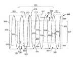
- FIG. 1illustrates a conventional electrode configuration that has been proposed for a projected capacitive touch screen.
- electrodes 101 - 105are formed of triangular regions of ITO or other transparent conductive film. Between electrodes 101 - 105 are insulating gaps often referred to as “deletion lines” as cost-effective manufacturing often starts with a glass substrate with a uniform ITO coating from which selected regions of ITO are removed to form the pattern of triangular electrodes 101 - 105 .
- Each electrode 101 - 105is electrically connected to the associated electronics, such as through metal traces indicated to the left of FIG. 1 .
- FIG. 2illustrates the edge deceleration effect that may be experienced by a projected capacitive touch screen with a small touch sensitive area 110 .
- FIG. 2illustrates a finger moving along a line or trajectory 128 while in contact with the touch screen surface. Finger contact areas 122 , 124 and 126 correspond to three different times during the finger motion along trajectory 128 .
- reconstructed (X,Y) touch coordinates 132 and 134will be at the center of the corresponding touch contact areas 122 and 124 .
- reconstructed (X,Y) touch coordinates 136which are not at the center of the touch contact area 126 . Instead, the reconstructed (X,Y) touch coordinates are at an “effective center” which is at the center of the on-screen portion or detected touch contact area within the touch sensitive area 110 .
- the trajectory 130 of reconstructed (X,Y) touch coordinates 136may deviate from the true finger trajectory 128 near the edge of the touch area producing an artificial deceleration of the measured finger motion velocity component that is perpendicular to the edge of the touch sensitive area 110 .
- a projected capacitive touch screencomprising a substrate and electrodes.
- the substratedefines an active touch zone surrounded by edges.
- the active touch zoneincludes a central active zone and an acceleration zone that is located proximate to, and extends along, at least one of the edges.
- the electrodesare provided on the substrate and are organized into first and second sets of electrodes that are contained within a common plane on the substrate.
- the first set of electrodesis interlaced with the second set of electrodes in a non-overlapping pattern on the substrate.
- At least a subset of the electrodeseach has an apex and a base and a non-uniform triangular shape that extends along a longitudinal axis between the apex and the base.
- the subset of the electrodesis located such that at least a portion of the non-uniform triangular shape is located within the acceleration zone.
- a projected capacitive touch screencomprising a substrate and electrodes.
- the substratedefines an active touch zone surrounded by edges.
- the active touch zoneincludes a central active zone and an acceleration zone that is located proximate to, and extends along, at least one of the edges.
- the electrodesare provided on the substrate and are organized into first and second sets of electrodes that are contained within a common plane on the substrate.
- the first set of electrodesis interlaced with the second set of electrodes in a non-overlapping pattern on the substrate. At least a subset of the electrodes each has opposed non-parallel first and second sides.
- the subset of the electrodeseach has an apex segment, a base segment and an intermediate body segment therebetween, wherein the first side has a first pitch in the intermediate segment and a second pitch in at least one of the apex and base segments.
- the subset of the electrodesis located such that at least one of the apex and base segments is located within the acceleration zone.
- an electronic devicecomprising a processor, memory storing instructions to control operation of the processor, and a display for presenting information to a user.
- the displayincludes a projected capacitive touch screen that comprises a substrate and electrodes.
- the substratedefines an active touch zone surrounded by edges.
- the active touch zoneincludes a central active zone and an acceleration zone that is located proximate to, and extends along, at least one of the edges.
- the electrodesare provided on the substrate and are organized into first and second sets of electrodes that are contained within a common plane on the substrate. The first set of electrodes is interlaced with the second set of electrodes in a non-overlapping pattern on the substrate.
- At least a subset of the electrodeseach has an apex and a base and a non-uniform triangular shape that extends along a longitudinal axis between the apex and the base.
- the subset of the electrodesis located such that at least a portion of the non-uniform triangular shape is located within the acceleration zone.
- the non-uniform triangular shapemay be formed in part by varying an electrode width more rapidly near a perimeter of the active touch zone than the variation of the electrode width near a center of the active touch zone.
- the non-uniform triangular shape and non-overlapping patternprovide edge acceleration to compensate for signal loss when a portion of a finger contact area moves beyond the edge outside of the active touch zone.
- the non-uniform triangular shapemay include a first pitch proximate to the base and a second pitch proximate to the apex. The pitch represents a rate of change in a width of the electrode per unit of distance along the longitudinal axis of the electrode.
- FIG. 1illustrates a conventional electrode configuration that has been proposed for a projected capacitive touch screen.
- FIG. 2illustrates an edge deceleration effect that may be experienced by a projected capacitive touch screen with a small touch sensitive area.
- FIG. 3illustrates a projected capacitive touch screen formed in accordance with an embodiment.
- FIG. 4Aillustrates an expanded view of one electrode to better illustrate a non-uniform triangular shape formed in accordance with one embodiment.
- FIG. 4Billustrates alternative geometries that may be utilized in the apex segment of electrodes in accordance with alternative embodiments.
- FIG. 5illustrates an electrode configuration with inter-electrode pitch differences formed in accordance with an alternative embodiment.
- FIG. 6illustrates a portion of a projected capacitive touch screen with electrode to contact groupings in accordance with one embodiment.
- FIG. 7illustrates a touch screen cross-section in accordance with an embodiment.
- FIG. 8illustrates a touch screen cross-section in accordance with another embodiment.
- FIG. 9illustrates an electronic system that implements a projected capacitive touch screen in accordance with an embodiment.
- FIG. 10illustrates alternative touch systems that may be implemented to utilize one or more projected capacitive touch screens formed in accordance with embodiments.
- FIG. 3illustrates a projected capacitive touch screen 300 that comprises a substrate 302 that defines an active touch zone 304 surrounded by edges 306 - 309 .
- the edges 306 - 309include lateral edges 306 and 308 that are located opposite one another on opposite sides of the active touch zone 304 and longitudinal edges 307 and 309 that are located opposite one another at the top and bottom of the active touch zone 304 .
- the touch screen 300operates in any orientation and that the terms “longitudinal”, “lateral”, “side”, “top” and “bottom” are for descriptive purposes only.
- the touch screen 300also includes a plurality of electrodes 310 - 326 provided on the substrate 302 .
- the electrodes 310 - 326are organized into a first set 310 - 317 and a second set 320 - 326 , where both the first and second sets 310 - 317 and 320 - 326 are both contained within a common plane on the substrate 302 .
- Each of the electrodes 310 - 326is electrically isolated from its nearest neighbors by deletion lines (as discussed above).
- the electrodes from the first set 310 - 317are interlaced with the electrodes from the second set 320 - 326 in a non-overlapping pattern on the substrate 302 that generally represents a backgammon type of pattern.
- Each of the electrodes 310 - 326has an apex 328 and a base 330 .
- Each of the electrodes 310 - 326is elongated to extend along a longitudinal axis 332 between the apex 328 and the base 330 .
- the longitudinal axes 332 of the electrodes 310 - 326are oriented to extend in a common direction as opposed lateral edges 306 and 308 . All of the electrodes 310 - 326 , or at least a subset of the electrodes 310 - 326 , have a non-uniform triangular shape or geometry, examples and the details of which are discussed below.
- the non-uniform triangular shapeprovides a desired “hardware edge acceleration” effect to compensate for the inherent edge deceleration effect discussed in connection with FIG. 2 .
- the non-uniform triangular shape and non-overlapping patternprovide edge acceleration to compensate for signal loss when a portion of a finger contact area moves beyond the edges 306 - 309 outside the active touch zone 304 .
- the electrodes 310 - 326include first and second subsets.
- the first subsetincludes electrodes 310 and 320 that extend along the acceleration zone 393 proximate the edge 308 .
- the first subsetalso includes electrodes 317 and 326 that extend along the acceleration zone 391 proximate the edge 306 .
- the second subset of electrodes 311 - 316 and 321 - 325extends through the central active zone 399 .
- the one or both of the first and second subsetsmay include only a single electrode.
- the electrodes 310 , 320 , 317 and 326 in the first subsethave a smaller electrode area than an electrode area of the electrodes 311 - 316 and 321 - 325 in the second subset. Exemplary differences in electrode area are discussed below in more detail in connection with FIG. 5 .
- An acceleration zonediffers from the central active zone in that at least a portion of the acceleration zone provides hardware edge acceleration while no hardware edge acceleration is present in the central active zone.
- the features of electrode design that produce hardware edge accelerationare illustrated in the figures.
- hardware edge acceleration, not hardware decelerationis required within the acceleration zone.
- Hardware accelerationis excluded or substantially absent from the central active zone where the edge deceleration effect of FIG. 2 is not present, as is desired to maintain the desired linear relationship between true and measured touch positions.
- the active touch zone 304includes a central active zone 399 as denoted in dashed line.
- the central active zone 399extends in the longitudinal direction 327 and in the lateral direction 329 .
- the active touch zone 304includes acceleration zones 391 , 393 , 395 and 397 that are located proximate to, and extend along, corresponding edges 306 , 308 , 397 and 309 , respectively.
- the central active zone 399is surrounded by the acceleration zones 391 , 393 , 395 and 397 .
- the electrodes 310 , 320 , and 311represent a subset of electrodes that are at least partially within, and that extend along, the acceleration zone 393 proximate to the edge 308 .
- the electrodes 325 , 317 and 326represent a subset of electrodes that are at least partially within, and that extend along, the acceleration zone 391 proximate to the edge 306 .
- the electrodes 311 - 316 , 321 - 325represent a subset of electrodes that are at least partially within, and that extend through, the central active zone such that the apexes 328 and bases 330 are located in opposed acceleration zones 395 and 397 .
- FIG. 4Aillustrates an expanded view of one electrode 339 to better illustrate one embodiment of a non-uniform triangular shape or geometry.
- the electrode 339 in FIG. 4Aincludes an apex 328 , a base 330 and a longitudinal axis 332 extending along a length of the electrode 339 .
- the electrode 339includes an electrode width, such as W 0 , W 1 and W 2 , that may be measured at various points along the length of the electrode 339 .
- the electrode width(generally denoted at 342 ) represents a local width of the electrode 339 between electrode sides 338 and 340 as measured in a lateral direction 345 perpendicular to the longitudinal axis 332 .
- the non-uniform triangular shapeis defined by multiple electrode widths that vary continuously at different points along the electrode 339 .
- the electrode 339is apportioned into foundation segment 351 , base segment 352 , intermediate body segment 353 and apex segment 354 .
- the electrode 339has opposed non-parallel sides 338 and 340 that extend between apex 328 and base 330 .
- the segments 351 - 354are differentiated from one another in that the pitch along one or both of the sides 338 and 340 changes between each of the segments 351 - 354 .
- the pitchrepresents a rate of change in the electrode width 342 per unit of distance along the length of longitudinal axis 332 of the electrode 339 .
- the non-uniform triangular shapeincludes a first pitch 346 along a base segment 352 proximate to the base 330 , a second pitch 348 along the intermediate body segment 353 and a third pitch 350 along the apex segment 354 proximate to the apex 328 .
- Pitchis defined with respect to the longitudinal axis 332 , namely pitch represents the change in lateral distance from longitudinal axis 332 per unit distance along longitudinal axis 332 .
- An intra-electrode pitchchanges (e.g., the pitch at different points along the electrode sides 338 and 340 ) such that the pitches 346 and 350 are the same, while pitch 348 differs from the pitches 346 and 350 .
- the pitch 348is decreased in rate relative to the pitches 346 and 350 when progressing from the intermediate body segment 353 towards an edge, namely to base 330 when progressing towards bottom edge 309 or to the apex 328 when progressing towards top edge 307 .
- the pitches 350 and 346are the same and both are greater than the pitch 348 .
- one or more of the pitches 346 , 348 and 350 along opposite sides 338 and 340may differ.
- the pitch along side 338 in segment 353may differ from the pitch along side 340 in the same segment 353 .
- the segments 351 - 354are formed contiguous with one another from a common base material, but may be conceptually considered distinct notional components having different size and with different pitches.
- the non-uniform triangular shapemay be considered to comprise a stack of trapezoids where the trapezoid nearest the apex 328 (e.g., apex segment 354 ) has a mid-point width that is less than a mid-point width of the trapezoid nearest the base 330 (e.g., base segment 352 ).
- the horizontal distance between left and right edges of electrodes 310 - 326varies with height. This variation becomes more rapid as the top and bottom edges 307 , 309 are approached.
- the more rapid the height variation of the electrode widththe more rapidly the fraction of the touch signal in the odd numbered electrodes increases as a function of touch position height, and hence a more rapid variation near the edges 307 , 309 provides a degree of hardware edge acceleration to compensate for the edge deceleration effect.
- There are many choices for the detailed geometry providing a more rapid height variation of electrode widthincluding straight-line segments of electrode perimeter in vertical regions, fewer or more such segments, as well as convex curved electrode outlines near the electrode apex 328 and matching concave curved electrode outlines near the electrode base 330 .
- the electrode 339is formed with four segments 351 - 354 with pitch changes therebetween.
- the number of segments with different pitchmay be fewer or more.
- each of the electrodes 310 - 326has two segments 363 and 364 with different pitch at the apex 328 and two segments 361 and 362 with different pitch at the base 330 .
- FIG. 4Billustrates alternative geometries that may be utilized in the apex segment of electrodes in accordance with alternative embodiments.
- apex segment 370includes a triangular contour with a pair of linear edge segments 372 that converge at point 374 .
- Apex segment 376includes multiple pairs of linear edge segments 378 and 379 that converge at a point 380 .
- Apex segment 382includes multiple pairs of linear edge segments 383 , 384 and 385 that converge at a point 386 .
- Apex segment 386includes a pair of rounded edge segments 387 forming a concave interior contour that converges to a point 388 .
- Apex segment 390includes a pair of rounded edges 391 that have a concave interior surface that meet at a concave end 392 .
- FIG. 5illustrates an electrode configuration with different electrode widths that may be used in accordance with an embodiment.
- FIG. 5illustrates a projected capacitive touch screen 400 that comprises a substrate 402 that defines an active touch zone 404 surrounded by edges 406 - 409 .
- the edges 406 - 409include lateral edges 406 and 408 that are located opposite one another on opposite sides of the active touch zone 404 , and longitudinal edges 407 and 409 are located opposite one another at the top and bottom of the active touch zone 404 .
- the active touch zone 404includes a central active zone 499 spanning in the longitudinal direction by 427 and in the lateral direction by 429 .
- the electrodes 410 - 427are organized into a first set 410 - 418 and a second set 420 - 427 , where both the first and second sets 410 - 418 and 420 - 427 are all contained within a common plane on the substrate 402 .
- the electrodes from the first set 420 - 428are interlaced with the electrodes from the second set 410 - 418 in a non-overlapping pattern on the substrate 402 that generally represents a backgammon type of pattern.
- Each of the electrodes 410 - 428has an apex 428 and a base 430 .
- Each of the electrodes 410 - 418is elongated to extend along a longitudinal axis 432 between the apex 428 and the base 430 . To avoid overly complicating FIG. 5 , only one longitudinal axis 432 is denoted.
- the longitudinal axes 432 of the electrodes 410 - 418are oriented to extend in a common direction as opposed lateral edges 406 , 408 . All of the electrodes 410 - 418 and 420 - 427 , or at least a subset of the electrodes 410 - 418 and 420 - 427 have a non-uniform triangular shape or geometry.
- the active touch zone 404includes lateral acceleration zones 401 and 403 that are located proximate to, and extend along, corresponding lateral edges 406 and 408 , respectively.
- the central active zone 499extends to the longitudinal edges 407 and 409 of the substrate 402 .
- the electrodes 410 , 411 , 420 and 421represent a subset that is wholly or at least partially within, and extends along, the acceleration zone 403 proximate to the edge 408 .
- electrode 410is located entirely within the acceleration zone 403
- electrode 421is located only partially within the acceleration zone 403 .
- the electrodes 417 , 418 , 426 , and 427represent a subset that is at least partially within, and extends along, the acceleration zone 401 proximate to the edge 406 .
- the electrodes 412 - 416 and 421 - 426represent a subset that is entirely or at least partially within, and extends through, the central active zone 499 between the longitudinal edges 407 and 409 .
- FIG. 5is drawn to illustrate triangles of uniform pitch but with non-uniformity in width to illustrate acceleration zones 401 and 403 proximate to edges 406 and 408 .
- designs with non-uniform pitch as in FIGS. 3 , 4 A and 4 Bmay be provided to afford acceleration on all sides.
- electrode widthsshould be small compared to the size of a contact area of a finger tip or other touch instrument.
- the electrode widths or pitches of at least a portion of the electrodes 410 - 418 and 420 - 427 shown in FIG. 5vary from one another.
- the electrodes 413 - 415 and 422 - 425have a common combination of pitches and a similar variation in electrode widths 442 as measured at the center longitudinal line 443 , while electrodes 410 - 412 , 416 - 418 , 420 - 421 , 426 - 427 near the left edge 408 and the right edge 406 are increasingly narrower in pitch and electrode width.
- the electrode width 444 of electrode 420 and the electrode width 445 of electrode 427 at central longitudinal line 443are less than the electrode width 442 of the central electrodes 413 - 415 at central longitudinal line 443 .
- the electrode width of the electrodes 427 and 420 at any longitudinal line across the substrate 402are less than the electrode width of the electrodes 422 - 425 at the same common longitudinal line.
- the surface area of the electrodesis a function of a spacing of the electrodes from the lateral edges 406 and 408 .
- the electrodes 413 - 415 and 422 - 425have a common surface area, referred to hereafter as electrode area.
- a portion of the electrodes that extend through the central active zone 499may have different electrode areas.
- electrodes 412 - 416 and 422 - 425are all at least partially within the central active zone 499 , they do not all have the same electrode area. Instead, the electrodes 412 and 416 have a single common electrode area, yet the electrode area of each of the electrodes 412 and 416 is less than the electrode area of each of the electrodes 413 - 415 .
- the electrodes 411 and 417have the same electrode area which is less than the electrode area of the electrodes 412 and 416 .
- the electrode area of the electrodes 420 and 427is the same but less than the electrode area of the electrodes 422 - 425 .
- each electrodemay be a function of the position or number of the electrode from the lateral edges 406 and 408 .
- the first electrodes in from the edges 408 and 406may have the least surface area, while the second electrodes in from the edges 408 and 406 may have slightly larger surface area.
- the surface area of the electrodesmay be the greatest in the center and progressively decrease for the electrodes located nearer and nearer the edges 406 and 408 .
- the choice of electrode widthsdepends on a number of criteria such as the typical contact area of touches, and the desired degree of edge acceleration desired to compensate for the edge deceleration effect. It is generally desirable for the electrode widths to decrease in the region proximate to the touch area edges.
- the change in electrode widthmay be an abrupt change from a larger electrode width to a smaller electrode width.
- the change in electrode widthmay be a linear decrease from electrode to electrode as a function of number of the electrode from the edge.
- Other schemesmay also be used for monotonically decreasing electrode width as the edge is approached.
- Edge accelerationresults from the decrease in electrode width or area in the acceleration zone relative to the central active zone 499 .
- the rate that the computed coordinate changes per unit horizontal movement of a finger touchis inversely proportional to the electrode width of areas.
- the rate that the computed horizontal coordinate changes as a function of finger motionhence providing edge acceleration.
- a horizontal coordinate estimate based on the sequence numbers of electrodes or electronic channels detecting a touch signala more rapid change in electrode or electronic channel number per physical unit of distance results in edge acceleration of the computed coordinate.
- Reducing electrode widths as in FIG. 5provides for hardware acceleration to compensate for the edge deceleration for two of the four edges of the active touch zone 404 , namely along the lateral edges 406 and 408 .
- one or more of the electrode geometries of FIGS. 3 , 4 A and 4 Bmay be combined with the variation in inter-electrode widths of FIG. 5 to provide hardware edge acceleration on all four edges 406 - 409 .
- Edge deceleration(as discussed above in connection with FIG. 2 ) is limited to a perimeter region of the active touch zone.
- the width of the perimeteris based, at least in part, on an estimated size of the finger contact area expected to touch the touch screen.
- the finger contact areamay typically have a diameter of up to 20 mm.
- the edge decelerationis limited to a region within 20 mm of the edges of the active touch zone.
- the hardware edge acceleration compensation methods discussed above in connection with FIGS. 3-5may be similarly limited to a region up to 20 mm from the edges of the active touch zone.
- the electrodes of narrowed width in FIG. 5may all be located within 20 mm of the lateral edges 406 and 408 .
- the apex and base segmentsmay be sized such that the heights of the apex and base segments are up to 20 mm in length to span the width of the longitudinal acceleration zones 395 , 397 .
- hardware edge accelerationmay be limited to a region less than or equal to 10 mm from the edges.
- edge acceleration zonesas small as 5 mm in width may be sufficient.
- hardware edge accelerationmay be combined with software edge correction algorithms. If the stylus activating the touchscreen is something bigger than a finger, say a palm or a foot, larger edge acceleration zones may be of interest.
- the central active zone 399need not be centered in the active touch zone 304 .
- the top, bottom and left acceleration zones 395 , 397 and 393may be provided, but no acceleration zone 391 may be provided along the right edge.
- top, right and left acceleration zones 395 , 391 and 393may be provided, but no acceleration zone 397 may be provided along the bottom edge.
- a width of one or more of the acceleration zones 391 , 393 , 395 and 397may differ from one another.
- the left acceleration zone 393may be wider (as measured laterally from the edge 308 ) than a width of the right acceleration zone 391 (as measured laterally from the edge 306 ).
- top and bottom acceleration zones 395 and 397may be wider (as measured longitudinally from the edges 307 and 309 ) than a width of the right and left acceleration zones 391 and 393 (as measured laterally from the edges 306 and 308 ).
- the hardware edge acceleration electrode configurations discussed in connection with FIGS. 3-5may be electrically coupled together in numerous different groups of common electrodes.
- the electrodesmay be grouped to enable the number of electrodes to greatly exceed the number of electronic channels that are separately processed by the touch screen electronics. When a limited number of electronic channels are available, using more electrodes than the number of channels improves the performance of the projected capacitive touch screen.
- FIG. 6illustrates a portion of a capacitive touch screen 600 with electrodes grouped in accordance with one embodiment.
- the electrodes 610are numbered # 0 to # 13 and are physically and electrically separated from adjacent electrodes at gaps 604 .
- the substrate 602may be glass, a polymer film such as polyethylene terephthalate (PET), or other suitable material.
- PETpolyethylene terephthalate
- Each of the electrodes 610may be formed from a deposited conductive coating that may be deposited in a desired pattern, such as by using screen printing, photographic, or other process. In another embodiment, the conductive coating may be deposited to evenly and completely cover a surface of the substrate 602 . Portions of the conductive coating may then be removed to form the triangular-shaped electrodes 610 .
- the transparent conductive coatingmay be indium tin oxide (ITO), antimony tin oxide (ATO), a fluorine-doped tin oxide, a carbon-nanotube containing film, a silver nano-wire containing film, an intrinsically conductive polymer, and the like.
- each of the electrodes 610may be formed by forming a serpentine pattern using fine metal wires to fill in an outline of each triangle such as described in U.S. Pat. No. 6,297,811, the complete subject matter of which is incorporated herein by reference.
- the wiresmay be, for example, between ten and twenty-five micrometers thick.
- the substrate 602includes an array of contacts 612 provided on opposite longitudinal edges 607 and 609 .
- the contacts 612are numbered # 0 to # 5 with the odd numbered contacts located along edge 609 and the evenly numbered contacts located along edge 607 .
- the electrodes 610include an apex 628 and a base 630 .
- the bases 630are electrically connected to corresponding contacts 612 .
- electrodes # 1 , # 3 , and # 5include bases 630 that are connected to contact # 1
- electrodes # 0 , and # 2include bases 630 that are connected to contact # 0 .
- the bases 630 of electrodes # 4 , # 6 and # 8are connected to contact # 2 , while the bases 630 of electrodes # 7 , # 9 and # 11 are connected to contact # 3 .
- two or three electrodes 610are connected to a common contact 612 .
- a single electrode 610may be connected in a one to one relation to a contact 612 .
- larger groups of electrodes 610may be connected to a single contact 612 .
- the contacts 612are connected to traces 630 - 635 that provide the sensed signals for the group of corresponding electrodes 612 to the controller 616 .
- traces 630 - 635may be formed from materials such as the conductive wire, silver-frit, deposited metal films, conductive-ink, incomplete deletion-line separation of the conductive coating, and the like, to electrically join electrodes 610 into groups on the substrate 602 .
- the traces 630 - 635may also convey signals and power between individual electrodes 610 and a cable or cable connector and/or the groups of electrodes and the cable or cable connector.
- adjacent electrodesrefers to nearest-neighbor electrodes that are next to each other.
- adjacent electrodesare numbered sequentially.
- electrodes # 1 and # 2are adjacent electrodes
- electrodes # 4 and # 5are adjacent electrodes.
- the orientation of adjacent electrodes # 0 to # 13is reversed or alternating with respect to each other, forming an interleaved arrangement.
- the base 630 of the electrode # 3is positioned adjacent to apex 628 of the adjacent electrodes # 2 and # 4 .
- a first set of odd-numbered electrodes # 1 , # 3 , # 5 , # 7 , # 9 , # 11 and # 13has an orientation wherein the bases 630 of the odd-numbered electrodes are all proximate the same edge, for example edge 609 of the substrate 602 .
- a second set of even-numbered electrodes # 0 , # 2 , # 4 , # 6 , # 8 , # 10 , and # 12has an opposite orientation compared to the orientation of the odd-numbered electrodes, wherein the bases 630 of the even-numbered electrodes are proximate the edge 607 of the substrate 122 .
- the term “semi-adjacent electrodes”refers to nearest-neighbor electrodes that have the same orientation.
- electrodes # 5 and # 7are semi-adjacent electrodes and electrodes # 8 and # 10 are semi-adjacent electrodes.
- Each of the traces 633 through 635forms a capacitance measuring electronic channel that is connected to a controller 616 and a set of semi-adjacent electrodes.
- semi-adjacent electrodes # 1 , # 3 , and # 5are joined at contact # 1 to provide a sensed signal over one channel (e.g. at trace 633 ).
- the touch screenmay include many more electrodes than are shown, thus providing more linear position measurements and/or a larger size touch screen.
- Electrodes 501may be attached to a substrate 503 . Electrodes 501 are coupled through interconnect traces 507 and a connection 505 , such as an anisotropic conductive film (ACF) adhesive bond, to a flexible cable 511 .
- the flexible cable 511in turn is coupled to touch screen electronics 509 .
- Touch surface 513may be of any dielectric material, such as glass, a polymer (e.g. polycarbonate). Touch surface 513 can even be designed for easy replacement for applications in which the touch surface is subject to significant wear or abuse, preferably transparent in typical applications with a display behind the touchscreen.
- touch surface 513can be mechanically coupled to the electrode array, for example with an adhesive layer 515 .
- a guard electrode 517can be deposited on the bottom surface of substrate 503 to minimize the effects of stray capacitances between the sense electrodes and, for example, a display device placed behind the touch screen.
- a perimeter guard electrodecan be provided in the plane of the sense electrodes to minimize the effects of stray capacitances to objects around the perimeter of the touch screen, e.g., metal associated with the bezel and its supporting structures.
- substrate 803serves as a touch surface and electrodes 801 are fabricated on the bottom or interior surface of substrate 803 . Electrodes 801 connect to electronics via conductive traces 807 , anisotropic adhesive film bond 805 and flexible cable 811 . This simple construct is of interest to applications requiring low cost designs.
- FIG. 9illustrates an electronic system that implements a projected capacitive touch screen in accordance with an embodiment herein.
- the electronic system 900may be embodied within a portable device or a stationary apparatus.
- the electronic systemmay constitute a cellular phone, a satellite navigation device, a portable computer, a video game, a personal digital assistant, a patient monitor, a workstation for a medical diagnostic imaging device and the like.
- the electronic system 900includes a display 902 that has a projected capacitive touch screen 904 , a processor 906 , a transceiver 908 , an accessory input 910 and memory 912 .
- the memory 912stores instructions to control the processor, outputs to the user, inputs from the user, inputs from accessories (e.g., ECG leads, a medical scanning device) and the like.
- FIG. 10illustrates alternative touch systems that may be implemented to utilize one or more projected capacitive touch screens formed in accordance with embodiments herein.
- FIG. 10illustrates a touch system 1010 having top, bottom, left and right borders 1012 - 1015 , respectively.
- the touch system 1010is formed by combining two different types of components, such as one type of component in region 1016 and a different type of component in region 1018 .
- the component in region 1016may represent a projected capacitive touch screen formed in accordance with one of the embodiments discussed above in connection with FIGS. 1-9 . While not illustrated, the region 1016 includes electrodes (e.g., as shown in FIGS.
- Electrodes 3-5provided on a substrate and organized into first and second sets of electrodes that are interlaced with one another in a non-overlapping pattern. At least a subset of the electrodes has an apex and a base and a non-uniform triangular shape that extends along a longitudinal axis between the apex and the base, where the non-uniform triangular shape is located within an acceleration zone along one of the edges.
- the component in region 1018may represent a different type of touch screen.
- the region 1018may include a touch screen that is formed based on another type of touch sensitive technology, such as surface acoustic wave, capacitive (non-projected), infrared, strain gauge, optical imaging, dispersive signal, acoustic pulse recognition, and the like. It may be desirable to utilize different types of touch sensitive technologies in combination in a touch system based on various factors such as the application, operating environment, user input instrument, information displayed, input requested from the user and the like.
- the characteristics and performance of a projected capacitive touch screenmay be desirable in a majority of the touch system (such as in region 1016 ), while the characteristics and performance of another touch sensitive technology are desirable in a smaller portion of the touch system (e.g., a stylus sensitive area to sign a name) (such as in region 1018 ).
- the region 1018may not be touch sensitive at all, but instead may simply include a display area, a keyboard, and the like.
- the touch system 1010may combine components in layouts that differ from regions 1016 and 1018 .
- corner regions 1020 - 1023(as denoted in dashed lines) may be provided with one type of touch sensitive technology, while a remaining portion of the touch system utilizes a different touch sensitive technology.
- the components in corner regions 1020 - 1023may represent projected capacitive touch screens formed in accordance with one of the embodiments discussed above in connection with FIGS. 1-9 .
- the component(s) in the remainder of the touch system 1010e.g., regions 1025 and 1030 - 1033 ) may be formed with a different type of touch technology.
- the entire touch system 1010may be formed utilizing a plurality of projected capacitive touch screens.
- the plurality of projected capacitive touch screensmay be arranged adjacent one another in an array, such as a 3 ⁇ 4 array as denoted by the dashed lines separating regions 1020 - 1023 , 1025 , and 1030 - 1033 .
- only a portion of the projected capacitive touch screensmay implement electrodes with a non-uniform triangular shape in accordance with one of the embodiments discussed above in connection with FIGS. 1-9 .
- only a subset of the regions 1020 - 1023 , 1025 , and 1030 - 1033may experience the deceleration effect discussed above.
- only the subset of the regions 1020 - 1023 , 1025 , and 1030 - 1033may implement hardware acceleration through non-uniform triangularly shaped electrodes.
Landscapes
- Engineering & Computer Science (AREA)
- General Engineering & Computer Science (AREA)
- Theoretical Computer Science (AREA)
- Human Computer Interaction (AREA)
- Physics & Mathematics (AREA)
- General Physics & Mathematics (AREA)
- Position Input By Displaying (AREA)
- User Interface Of Digital Computer (AREA)
Abstract
Description
Claims (20)
Priority Applications (5)
| Application Number | Priority Date | Filing Date | Title |
|---|---|---|---|
| US12/471,194US8279194B2 (en) | 2009-05-22 | 2009-05-22 | Electrode configurations for projected capacitive touch screen |
| PCT/US2010/001321WO2010134948A1 (en) | 2009-05-22 | 2010-05-03 | Electrode configurations for projected capacitive touch screen |
| DE112010002067TDE112010002067T5 (en) | 2009-05-22 | 2010-05-03 | Electrode configurations for projected capacitive touchscreen |
| CN2010800224074ACN102439551A (en) | 2009-05-22 | 2010-05-03 | Electrode configurations for projected capacitive touch screen |
| TW099116078ATW201101161A (en) | 2009-05-22 | 2010-05-20 | Electrode configurations for projected capacitive touch screen |
Applications Claiming Priority (1)
| Application Number | Priority Date | Filing Date | Title |
|---|---|---|---|
| US12/471,194US8279194B2 (en) | 2009-05-22 | 2009-05-22 | Electrode configurations for projected capacitive touch screen |
Publications (2)
| Publication Number | Publication Date |
|---|---|
| US20100295814A1 US20100295814A1 (en) | 2010-11-25 |
| US8279194B2true US8279194B2 (en) | 2012-10-02 |
Family
ID=42334041
Family Applications (1)
| Application Number | Title | Priority Date | Filing Date |
|---|---|---|---|
| US12/471,194Expired - Fee RelatedUS8279194B2 (en) | 2009-05-22 | 2009-05-22 | Electrode configurations for projected capacitive touch screen |
Country Status (5)
| Country | Link |
|---|---|
| US (1) | US8279194B2 (en) |
| CN (1) | CN102439551A (en) |
| DE (1) | DE112010002067T5 (en) |
| TW (1) | TW201101161A (en) |
| WO (1) | WO2010134948A1 (en) |
Cited By (18)
| Publication number | Priority date | Publication date | Assignee | Title |
|---|---|---|---|---|
| US20120001863A1 (en)* | 2010-07-02 | 2012-01-05 | Samsung Electro-Mechanics Co., Ltd. | Touch panel |
| US20120222498A1 (en)* | 2011-03-04 | 2012-09-06 | Hm Technology International Limited | Force Sensor |
| US20120256873A1 (en)* | 2011-04-06 | 2012-10-11 | Sitronix Technology Corp. | Sensing structure of touch panel |
| US20130069907A1 (en)* | 2011-09-16 | 2013-03-21 | Jane Hsu | Projected capacitive touch panel with accelerated touch response time |
| US8410795B1 (en) | 2012-03-16 | 2013-04-02 | Cypress Semiconductor Corporation | Serpentine touch sensor pattern |
| US20140210764A1 (en)* | 2009-12-18 | 2014-07-31 | Synaptics Incorporated | Input device |
| WO2015026455A1 (en) | 2013-08-20 | 2015-02-26 | Carestream Health, Inc. | Patterning of electrically conductive films |
| WO2015061009A1 (en) | 2013-10-21 | 2015-04-30 | Carestream Health, Inc. | Invisible patterns for transparent electrically conductive films |
| US10078406B2 (en) | 2016-03-31 | 2018-09-18 | Synaptics Incorporated | Capacitive side position extrapolation |
| US10124767B1 (en) | 2018-01-29 | 2018-11-13 | Ford Global Technologies, Llc | Vehicle exterior keypad having interior lamp |
| US10279659B2 (en) | 2017-01-12 | 2019-05-07 | Ford Global Technologies, Llc | Vehicle keypad formed in a window |
| US10466839B2 (en) | 2016-03-30 | 2019-11-05 | Synaptics Incorporated | Dynamic differential algorithm for side touch signals |
| US20220317817A1 (en)* | 2021-03-30 | 2022-10-06 | Samsung Display Co., Ltd. | Electronic device |
| US11468749B2 (en)* | 2016-06-12 | 2022-10-11 | Apple Inc. | Devices, methods, and graphical user interfaces for providing haptic feedback |
| US11662824B2 (en) | 2016-09-06 | 2023-05-30 | Apple Inc. | Devices, methods, and graphical user interfaces for generating tactile outputs |
| US11674914B2 (en) | 2021-11-16 | 2023-06-13 | Baker Hughes Holdings Llc | Impedance sensor |
| US11790739B2 (en) | 2014-09-02 | 2023-10-17 | Apple Inc. | Semantic framework for variable haptic output |
| US12353631B2 (en) | 2016-06-12 | 2025-07-08 | Apple Inc. | Devices, methods, and graphical user interfaces for providing haptic feedback |
Families Citing this family (36)
| Publication number | Priority date | Publication date | Assignee | Title |
|---|---|---|---|---|
| US20090315570A1 (en)* | 2008-06-23 | 2009-12-24 | Mark Lynsin David Chappell | Capacitive sensing device |
| US20100295813A1 (en)* | 2009-05-22 | 2010-11-25 | Tyco Electronics Corporation | System and method for a projected capacitive touchscreen having grouped electrodes |
| US8456443B2 (en)* | 2009-07-24 | 2013-06-04 | Synaptics Incorporated | Single-layer touch sensors |
| US8477106B2 (en)* | 2009-07-29 | 2013-07-02 | Elo Touch Solutions, Inc. | System and method for a projected capacitive touchscreen having weight based coordinate determination |
| US8390591B2 (en)* | 2010-11-22 | 2013-03-05 | Integrated Device Technology, Inc. | Proportional area weighted sensor for two-dimensional locations on a touch-screen |
| US10001883B2 (en) | 2010-12-22 | 2018-06-19 | Elo Touch Solutions, Inc. | Mechanical deflection compensation for a capacitive touch input device |
| US9152278B2 (en) | 2010-12-22 | 2015-10-06 | Elo Touch Solutions, Inc. | Background capacitance compensation for a capacitive touch input device |
| TWM417612U (en)* | 2011-06-03 | 2011-12-01 | Sentelic Corp | Capacitance type touch control keyboard and touch control conduction structure thereof |
| KR101363361B1 (en)* | 2011-07-06 | 2014-02-14 | (주)멜파스 | Panel for sensing touch input |
| US8988086B1 (en) | 2011-08-10 | 2015-03-24 | Cypress Semiconductor Corporation | Capacitive sensor array with pattern variation |
| CN103019428A (en)* | 2011-09-27 | 2013-04-03 | 安浙触控科技有限公司 | touch panel |
| US9594504B2 (en)* | 2011-11-08 | 2017-03-14 | Microsoft Technology Licensing, Llc | User interface indirect interaction |
| CA2892615C (en)* | 2011-12-09 | 2020-05-12 | Hm Technology International Limited | Capacitive matrix sensor for measuring permittivity of an object |
| WO2013083952A1 (en)* | 2011-12-09 | 2013-06-13 | Hm Technology International Limited | Capacitive matrix sensor for measuring permittivity of an object |
| CN103197784B (en) | 2012-01-06 | 2016-05-25 | 宸鸿科技(厦门)有限公司 | Contact panel and preparation method thereof |
| CN103327729B (en)* | 2012-03-22 | 2016-03-23 | 瀚宇彩晶股份有限公司 | Flexible printed circuit board bonding structure for electronic devices |
| TWI484395B (en) | 2012-07-25 | 2015-05-11 | Mstar Semiconductor Inc | Self-capacitive touch panel |
| CN102789347A (en)* | 2012-07-30 | 2012-11-21 | 潘兴修 | Wholly transparent capacitive touch screen |
| CN103577006B (en)* | 2012-08-07 | 2016-09-28 | 晨星软件研发(深圳)有限公司 | self-capacitance type touch panel |
| TWI486851B (en)* | 2012-08-17 | 2015-06-01 | Mstar Semiconductor Inc | Self-capacitive touch panel |
| CN103677454B (en)* | 2012-09-04 | 2016-09-14 | 晨星软件研发(深圳)有限公司 | self-capacitance type touch panel |
| US9329731B2 (en)* | 2012-09-12 | 2016-05-03 | Synaptics Incorporated | Routing trace compensation |
| KR102077316B1 (en) | 2012-11-14 | 2020-04-08 | 삼성디스플레이 주식회사 | flexible touch screen panel and flexible display device with the same |
| CN103186304B (en)* | 2013-01-21 | 2016-01-27 | 敦泰科技有限公司 | Single-layer self-capacitance touch screen for realizing multi-touch recognition and data processing method thereof |
| CN104615325A (en)* | 2013-01-21 | 2015-05-13 | 敦泰科技有限公司 | Single-layer self-capacitance touch screen for realizing multi-point touch identification and data processing method thereof |
| JP2014186537A (en) | 2013-03-22 | 2014-10-02 | Japan Display Inc | Display device, and electronic apparatus |
| JP5943023B2 (en)* | 2013-07-08 | 2016-06-29 | 凸版印刷株式会社 | Touch sensor electrode, touch panel, and display device |
| JP5832489B2 (en)* | 2013-08-26 | 2015-12-16 | 株式会社コナミデジタルエンタテインメント | Movement control apparatus and program |
| CN104516561A (en)* | 2013-09-29 | 2015-04-15 | 宸鸿光电科技股份有限公司 | Touch panel and touch display |
| US9436324B2 (en) | 2013-11-04 | 2016-09-06 | Blackberry Limited | Electronic device including touch-sensitive display and method of detecting touches |
| TWI493412B (en)* | 2013-11-22 | 2015-07-21 | Mstar Semiconductor Inc | Sensing electrode structure |
| KR20150112233A (en)* | 2014-03-27 | 2015-10-07 | 삼성전기주식회사 | Touch Sensor Module |
| US9977555B2 (en)* | 2014-08-11 | 2018-05-22 | 3M Innovative Properties Company | Capacitive touch sensor apparatus |
| DE102014221071A1 (en)* | 2014-10-16 | 2016-04-21 | Continental Automotive Gmbh | Method for operating a touch-sensitive input field |
| KR101931897B1 (en)* | 2015-01-16 | 2018-12-21 | 알프스 덴키 가부시키가이샤 | Capacitive sensor |
| US10928946B2 (en)* | 2019-02-15 | 2021-02-23 | Dell Products L.P. | Touchscreen stylus and display module interface |
Citations (40)
| Publication number | Priority date | Publication date | Assignee | Title |
|---|---|---|---|---|
| US4087625A (en) | 1976-12-29 | 1978-05-02 | International Business Machines Corporation | Capacitive two dimensional tablet with single conductive layer |
| US4103252A (en) | 1976-11-26 | 1978-07-25 | Xerox Corporation | Capacitive touch-activated transducer system including a plurality of oscillators |
| US4495485A (en) | 1980-12-12 | 1985-01-22 | General Electric Company | Touch control arrangement for data entry |
| US4659874A (en) | 1985-09-23 | 1987-04-21 | Sanders Associates, Inc. | X-Y position sensor |
| US4686332A (en) | 1986-06-26 | 1987-08-11 | International Business Machines Corporation | Combined finger touch and stylus detection system for use on the viewing surface of a visual display device |
| WO1988005577A1 (en) | 1987-01-15 | 1988-07-28 | Ronald Peter Binstead | Improvements in or relating to touch keypad systems |
| US4778951A (en) | 1983-09-12 | 1988-10-18 | Peptek, Inc. | Arrays of resistive elements for use in touch panels and for producing electric fields |
| US4954823A (en) | 1984-04-17 | 1990-09-04 | Binstead Ronald P | Touch keyboard systems |
| US4980519A (en) | 1990-03-02 | 1990-12-25 | The Board Of Trustees Of The Leland Stanford Jr. Univ. | Three dimensional baton and gesture sensor |
| US4999462A (en) | 1989-10-06 | 1991-03-12 | Summagraphics Corporation | Position determining and digitizing method and device |
| US5117071A (en) | 1990-10-31 | 1992-05-26 | International Business Machines Corporation | Stylus sensing system |
| WO1996015464A1 (en) | 1994-11-14 | 1996-05-23 | Moonstone Technology Limited | Capacitive touch detectors |
| US5650597A (en) | 1995-01-20 | 1997-07-22 | Dynapro Systems, Inc. | Capacitive touch sensor |
| US5694154A (en) | 1994-11-08 | 1997-12-02 | International Business Machines Corporation | Touch sensor input system for a computer display |
| US5844506A (en) | 1994-04-05 | 1998-12-01 | Binstead; Ronald Peter | Multiple input proximity detector and touchpad system |
| US5847690A (en) | 1995-10-24 | 1998-12-08 | Lucent Technologies Inc. | Integrated liquid crystal display and digitizer having a black matrix layer adapted for sensing screen touch location |
| US6288707B1 (en) | 1996-07-29 | 2001-09-11 | Harald Philipp | Capacitive position sensor |
| US6297811B1 (en)* | 1999-06-02 | 2001-10-02 | Elo Touchsystems, Inc. | Projective capacitive touchscreen |
| US6537150B1 (en) | 1999-03-29 | 2003-03-25 | Sierra Design Group | Gaming devices having reverse-mapped game set |
| US6787715B2 (en) | 1999-11-01 | 2004-09-07 | Aiptek International Inc. | N-shaped antenna loops of digitizer tablet for reducing antenna switches and the method for locating the cordless pen |
| US6879930B2 (en) | 2001-03-30 | 2005-04-12 | Microsoft Corporation | Capacitance touch slider |
| US20060097991A1 (en) | 2004-05-06 | 2006-05-11 | Apple Computer, Inc. | Multipoint touchscreen |
| US20060244732A1 (en) | 2005-04-28 | 2006-11-02 | Geaghan Bernard O | Touch location determination using bending mode sensors and multiple detection techniques |
| US7218124B1 (en) | 2006-01-30 | 2007-05-15 | Synaptics Incorporated | Capacitive sensing apparatus designs |
| US20070247443A1 (en) | 2006-04-25 | 2007-10-25 | Harald Philipp | Hybrid Capacitive Touch Screen Element |
| US20070257894A1 (en) | 2006-05-05 | 2007-11-08 | Harald Philipp | Touch Screen Element |
| US20070279395A1 (en) | 2006-05-31 | 2007-12-06 | Harald Philipp | Two Dimensional Position Sensor |
| US20080074398A1 (en) | 2006-09-26 | 2008-03-27 | David Gordon Wright | Single-layer capacitive sensing device |
| US20080246496A1 (en) | 2007-04-05 | 2008-10-09 | Luben Hristov | Two-Dimensional Position Sensor |
| US20080259044A1 (en) | 2007-04-20 | 2008-10-23 | Seiko Epson Corporation | Coordinate input device and display device |
| EP2045698A2 (en) | 2007-10-04 | 2009-04-08 | Apple Inc. | Single-layer touch-sensitive display |
| US20090194344A1 (en) | 2008-01-31 | 2009-08-06 | Avago Technologies Ecbu Ip (Singapore) Pte. Ltd. | Single Layer Mutual Capacitance Sensing Systems, Device, Components and Methods |
| US20090303231A1 (en)* | 2008-06-09 | 2009-12-10 | Fabrice Robinet | Touch Screen Device, Method, and Graphical User Interface for Manipulating Three-Dimensional Virtual Objects |
| US20100001973A1 (en) | 2008-07-03 | 2010-01-07 | Apple Inc. | Display with dual-function capacitive elements |
| US20100000675A1 (en) | 2008-07-01 | 2010-01-07 | Samsung Techwin Co., Ltd. | Method and apparatus for manufacturing multi-layer substrate |
| US20100051355A1 (en) | 2008-08-31 | 2010-03-04 | Kai-Ti Yang | Capacitive touch panel |
| US20100079393A1 (en) | 2008-10-01 | 2010-04-01 | Integrated Device Technology, Inc. | Alternating, complementary conductive element pattern for multi-touch sensor |
| US20100295813A1 (en) | 2009-05-22 | 2010-11-25 | Tyco Electronics Corporation | System and method for a projected capacitive touchscreen having grouped electrodes |
| US20110025636A1 (en) | 2008-04-04 | 2011-02-03 | Melfas, Inc. | Contact sensing device with improved edge position recognition characteristics |
| US20110141051A1 (en) | 2008-08-14 | 2011-06-16 | Melfas, Inc. | Touch sensing panel including bidirectional adjacent electrodes, and touch sensing apparatus |
Family Cites Families (2)
| Publication number | Priority date | Publication date | Assignee | Title |
|---|---|---|---|---|
| US7382139B2 (en)* | 2004-06-03 | 2008-06-03 | Synaptics Incorporated | One layer capacitive sensing apparatus having varying width sensing elements |
| GB0912379D0 (en)* | 2009-07-17 | 2009-08-26 | Rolls Royce Plc | Rotary coupling |
- 2009
- 2009-05-22USUS12/471,194patent/US8279194B2/ennot_activeExpired - Fee Related
- 2010
- 2010-05-03DEDE112010002067Tpatent/DE112010002067T5/ennot_activeWithdrawn
- 2010-05-03CNCN2010800224074Apatent/CN102439551A/enactivePending
- 2010-05-03WOPCT/US2010/001321patent/WO2010134948A1/enactiveApplication Filing
- 2010-05-20TWTW099116078Apatent/TW201101161A/enunknown
Patent Citations (41)
| Publication number | Priority date | Publication date | Assignee | Title |
|---|---|---|---|---|
| US4103252A (en) | 1976-11-26 | 1978-07-25 | Xerox Corporation | Capacitive touch-activated transducer system including a plurality of oscillators |
| US4087625A (en) | 1976-12-29 | 1978-05-02 | International Business Machines Corporation | Capacitive two dimensional tablet with single conductive layer |
| US4495485A (en) | 1980-12-12 | 1985-01-22 | General Electric Company | Touch control arrangement for data entry |
| US4778951A (en) | 1983-09-12 | 1988-10-18 | Peptek, Inc. | Arrays of resistive elements for use in touch panels and for producing electric fields |
| US4954823A (en) | 1984-04-17 | 1990-09-04 | Binstead Ronald P | Touch keyboard systems |
| US4659874A (en) | 1985-09-23 | 1987-04-21 | Sanders Associates, Inc. | X-Y position sensor |
| US4686332A (en) | 1986-06-26 | 1987-08-11 | International Business Machines Corporation | Combined finger touch and stylus detection system for use on the viewing surface of a visual display device |
| WO1988005577A1 (en) | 1987-01-15 | 1988-07-28 | Ronald Peter Binstead | Improvements in or relating to touch keypad systems |
| US4999462A (en) | 1989-10-06 | 1991-03-12 | Summagraphics Corporation | Position determining and digitizing method and device |
| US4980519A (en) | 1990-03-02 | 1990-12-25 | The Board Of Trustees Of The Leland Stanford Jr. Univ. | Three dimensional baton and gesture sensor |
| US5117071A (en) | 1990-10-31 | 1992-05-26 | International Business Machines Corporation | Stylus sensing system |
| US5844506A (en) | 1994-04-05 | 1998-12-01 | Binstead; Ronald Peter | Multiple input proximity detector and touchpad system |
| US5694154A (en) | 1994-11-08 | 1997-12-02 | International Business Machines Corporation | Touch sensor input system for a computer display |
| WO1996015464A1 (en) | 1994-11-14 | 1996-05-23 | Moonstone Technology Limited | Capacitive touch detectors |
| US20030067451A1 (en) | 1994-11-14 | 2003-04-10 | James Peter Tagg | Capacitive touch detectors |
| US5650597A (en) | 1995-01-20 | 1997-07-22 | Dynapro Systems, Inc. | Capacitive touch sensor |
| US5847690A (en) | 1995-10-24 | 1998-12-08 | Lucent Technologies Inc. | Integrated liquid crystal display and digitizer having a black matrix layer adapted for sensing screen touch location |
| US6288707B1 (en) | 1996-07-29 | 2001-09-11 | Harald Philipp | Capacitive position sensor |
| US6537150B1 (en) | 1999-03-29 | 2003-03-25 | Sierra Design Group | Gaming devices having reverse-mapped game set |
| US6297811B1 (en)* | 1999-06-02 | 2001-10-02 | Elo Touchsystems, Inc. | Projective capacitive touchscreen |
| US6787715B2 (en) | 1999-11-01 | 2004-09-07 | Aiptek International Inc. | N-shaped antenna loops of digitizer tablet for reducing antenna switches and the method for locating the cordless pen |
| US6879930B2 (en) | 2001-03-30 | 2005-04-12 | Microsoft Corporation | Capacitance touch slider |
| US20060097991A1 (en) | 2004-05-06 | 2006-05-11 | Apple Computer, Inc. | Multipoint touchscreen |
| US20060244732A1 (en) | 2005-04-28 | 2006-11-02 | Geaghan Bernard O | Touch location determination using bending mode sensors and multiple detection techniques |
| US7218124B1 (en) | 2006-01-30 | 2007-05-15 | Synaptics Incorporated | Capacitive sensing apparatus designs |
| US20070247443A1 (en) | 2006-04-25 | 2007-10-25 | Harald Philipp | Hybrid Capacitive Touch Screen Element |
| US20070257894A1 (en) | 2006-05-05 | 2007-11-08 | Harald Philipp | Touch Screen Element |
| US20070279395A1 (en) | 2006-05-31 | 2007-12-06 | Harald Philipp | Two Dimensional Position Sensor |
| US20080074398A1 (en) | 2006-09-26 | 2008-03-27 | David Gordon Wright | Single-layer capacitive sensing device |
| US20080246496A1 (en) | 2007-04-05 | 2008-10-09 | Luben Hristov | Two-Dimensional Position Sensor |
| US20080259044A1 (en) | 2007-04-20 | 2008-10-23 | Seiko Epson Corporation | Coordinate input device and display device |
| EP2045698A2 (en) | 2007-10-04 | 2009-04-08 | Apple Inc. | Single-layer touch-sensitive display |
| US20090194344A1 (en) | 2008-01-31 | 2009-08-06 | Avago Technologies Ecbu Ip (Singapore) Pte. Ltd. | Single Layer Mutual Capacitance Sensing Systems, Device, Components and Methods |
| US20110025636A1 (en) | 2008-04-04 | 2011-02-03 | Melfas, Inc. | Contact sensing device with improved edge position recognition characteristics |
| US20090303231A1 (en)* | 2008-06-09 | 2009-12-10 | Fabrice Robinet | Touch Screen Device, Method, and Graphical User Interface for Manipulating Three-Dimensional Virtual Objects |
| US20100000675A1 (en) | 2008-07-01 | 2010-01-07 | Samsung Techwin Co., Ltd. | Method and apparatus for manufacturing multi-layer substrate |
| US20100001973A1 (en) | 2008-07-03 | 2010-01-07 | Apple Inc. | Display with dual-function capacitive elements |
| US20110141051A1 (en) | 2008-08-14 | 2011-06-16 | Melfas, Inc. | Touch sensing panel including bidirectional adjacent electrodes, and touch sensing apparatus |
| US20100051355A1 (en) | 2008-08-31 | 2010-03-04 | Kai-Ti Yang | Capacitive touch panel |
| US20100079393A1 (en) | 2008-10-01 | 2010-04-01 | Integrated Device Technology, Inc. | Alternating, complementary conductive element pattern for multi-touch sensor |
| US20100295813A1 (en) | 2009-05-22 | 2010-11-25 | Tyco Electronics Corporation | System and method for a projected capacitive touchscreen having grouped electrodes |
Non-Patent Citations (2)
| Title |
|---|
| International Preliminary Report on Patentability dated Dec. 1, 2011 for PCT/US2010/001321. |
| International Search Report of PCT/US2010/001321 (counterpart of U.S. Appl. No. 12/471,194). |
Cited By (28)
| Publication number | Priority date | Publication date | Assignee | Title |
|---|---|---|---|---|
| US9880209B2 (en) | 2009-12-18 | 2018-01-30 | Synaptics Incorporated | Capacitive sensing on large touch screens |
| US9606676B2 (en)* | 2009-12-18 | 2017-03-28 | Synaptics Incorporated | Input device |
| US9354264B2 (en) | 2009-12-18 | 2016-05-31 | Synaptics Incorporated | Transcapacitive sensor devices with seams |
| US20140210764A1 (en)* | 2009-12-18 | 2014-07-31 | Synaptics Incorporated | Input device |
| US20120001863A1 (en)* | 2010-07-02 | 2012-01-05 | Samsung Electro-Mechanics Co., Ltd. | Touch panel |
| US8857274B2 (en)* | 2011-03-04 | 2014-10-14 | Hm Technology International Limited | Force sensor |
| US20120222498A1 (en)* | 2011-03-04 | 2012-09-06 | Hm Technology International Limited | Force Sensor |
| US8907919B2 (en)* | 2011-04-06 | 2014-12-09 | Sitronix Technology Corp. | Sensing structure of touch panel |
| US20120256873A1 (en)* | 2011-04-06 | 2012-10-11 | Sitronix Technology Corp. | Sensing structure of touch panel |
| US20130069907A1 (en)* | 2011-09-16 | 2013-03-21 | Jane Hsu | Projected capacitive touch panel with accelerated touch response time |
| US8436627B1 (en)* | 2012-03-16 | 2013-05-07 | Cypress Semiconductor Corporation | Serpentine touch sensor pattern |
| US8410795B1 (en) | 2012-03-16 | 2013-04-02 | Cypress Semiconductor Corporation | Serpentine touch sensor pattern |
| WO2015026455A1 (en) | 2013-08-20 | 2015-02-26 | Carestream Health, Inc. | Patterning of electrically conductive films |
| WO2015061009A1 (en) | 2013-10-21 | 2015-04-30 | Carestream Health, Inc. | Invisible patterns for transparent electrically conductive films |
| US12300095B2 (en) | 2014-09-02 | 2025-05-13 | Apple Inc. | Semantic framework for variable haptic output |
| US11790739B2 (en) | 2014-09-02 | 2023-10-17 | Apple Inc. | Semantic framework for variable haptic output |
| US10466839B2 (en) | 2016-03-30 | 2019-11-05 | Synaptics Incorporated | Dynamic differential algorithm for side touch signals |
| US10078406B2 (en) | 2016-03-31 | 2018-09-18 | Synaptics Incorporated | Capacitive side position extrapolation |
| US11468749B2 (en)* | 2016-06-12 | 2022-10-11 | Apple Inc. | Devices, methods, and graphical user interfaces for providing haptic feedback |
| US11735014B2 (en) | 2016-06-12 | 2023-08-22 | Apple Inc. | Devices, methods, and graphical user interfaces for providing haptic feedback |
| US12190714B2 (en) | 2016-06-12 | 2025-01-07 | Apple Inc. | Devices, methods, and graphical user interfaces for providing haptic feedback |
| US12353631B2 (en) | 2016-06-12 | 2025-07-08 | Apple Inc. | Devices, methods, and graphical user interfaces for providing haptic feedback |
| US11662824B2 (en) | 2016-09-06 | 2023-05-30 | Apple Inc. | Devices, methods, and graphical user interfaces for generating tactile outputs |
| US10279659B2 (en) | 2017-01-12 | 2019-05-07 | Ford Global Technologies, Llc | Vehicle keypad formed in a window |
| US10124767B1 (en) | 2018-01-29 | 2018-11-13 | Ford Global Technologies, Llc | Vehicle exterior keypad having interior lamp |
| US20220317817A1 (en)* | 2021-03-30 | 2022-10-06 | Samsung Display Co., Ltd. | Electronic device |
| US11714514B2 (en)* | 2021-03-30 | 2023-08-01 | Samsung Display Co., Ltd. | Electronic device |
| US11674914B2 (en) | 2021-11-16 | 2023-06-13 | Baker Hughes Holdings Llc | Impedance sensor |
Also Published As
| Publication number | Publication date |
|---|---|
| TW201101161A (en) | 2011-01-01 |
| DE112010002067T5 (en) | 2012-07-19 |
| WO2010134948A1 (en) | 2010-11-25 |
| US20100295814A1 (en) | 2010-11-25 |
| CN102439551A (en) | 2012-05-02 |
Similar Documents
| Publication | Publication Date | Title |
|---|---|---|
| US8279194B2 (en) | Electrode configurations for projected capacitive touch screen | |
| US10338759B1 (en) | Sense electrode design | |
| US8698029B2 (en) | Touch sensor and method of forming a touch sensor | |
| US10969909B2 (en) | Touch screen panel and touch sensing apparatus having the same | |
| KR102456154B1 (en) | Sensor, touch sensor and display device | |
| US9727175B2 (en) | System and method for detecting locations of touches on a projected capacitive touch sensor | |
| US9836167B2 (en) | Electrode layout for touch screens | |
| US20100295813A1 (en) | System and method for a projected capacitive touchscreen having grouped electrodes | |
| US9383848B2 (en) | Interleaved piezoelectric tactile interface | |
| JP4869309B2 (en) | Touch screen, touch panel and display device | |
| JP5636768B2 (en) | Information input device | |
| US20030234771A1 (en) | Capacitive touch sensor architecture with unique sensor bar addressing | |
| US20170060331A1 (en) | Touch screen panel, touch sensing apparatus having the same and driving method thereof | |
| US20240427455A1 (en) | Touch input device | |
| US20100079384A1 (en) | Capacitance touch screen | |
| US20140035864A1 (en) | Capacitive touch-control panel and apparatus thereof | |
| US20110279406A1 (en) | Capacitance sensor and information input apparatus | |
| US20110205172A1 (en) | Touch screen device | |
| JP2007018515A (en) | Two-dimensional position sensor | |
| US10802655B2 (en) | Touch panel and touch panel device | |
| JP2014002540A (en) | Touch panel sensor and information processing device | |
| US10528185B2 (en) | Floating touch method and touch device | |
| CN108415632B (en) | Touch panel and touch button | |
| US9170614B2 (en) | Touch input device | |
| CN105027038B (en) | Device, method and system for correcting tail effect |
Legal Events
| Date | Code | Title | Description |
|---|---|---|---|
| AS | Assignment | Owner name:TYCO ELECTRONICS CORPORATION, PENNSYLVANIA Free format text:ASSIGNMENT OF ASSIGNORS INTEREST;ASSIGNORS:KENT, JOEL C.;AROYAN, JAMES L.;REEL/FRAME:023218/0511 Effective date:20090724 | |
| AS | Assignment | Owner name:ELO TOUCH SOLUTIONS, INC., CALIFORNIA Free format text:ASSIGNMENT OF ASSIGNORS INTEREST;ASSIGNOR:TYCO ELECTRONICS CORPORATION;REEL/FRAME:028357/0655 Effective date:20120601 | |
| AS | Assignment | Owner name:CREDIT SUISSE AG, NEW YORK Free format text:PATENT SECURITY AGREEMENT (FIRST LIEN);ASSIGNOR:ELO TOUCH SOLUTIONS, INC.;REEL/FRAME:028486/0917 Effective date:20120601 | |
| AS | Assignment | Owner name:CREDIT SUISSE AG, NEW YORK Free format text:PATENT SECURITY AGREEMENT (SECOND LIEN);ASSIGNOR:ELO TOUCH SOLUTIONS, INC.;REEL/FRAME:028486/0941 Effective date:20120601 | |
| STCF | Information on status: patent grant | Free format text:PATENTED CASE | |
| FPAY | Fee payment | Year of fee payment:4 | |
| AS | Assignment | Owner name:JPMORGAN CHASE BANK, N.A., AS COLLATERAL AGENT, NEW YORK Free format text:SECURITY AGREEMENT;ASSIGNOR:ELO TOUCH SOLUTIONS, INC.;REEL/FRAME:044652/0421 Effective date:20171031 Owner name:JPMORGAN CHASE BANK, N.A., AS COLLATERAL AGENT, NE Free format text:SECURITY AGREEMENT;ASSIGNOR:ELO TOUCH SOLUTIONS, INC.;REEL/FRAME:044652/0421 Effective date:20171031 | |
| AS | Assignment | Owner name:ELO TOUCH SOLUTIONS, INC., CALIFORNIA Free format text:RELEASE BY SECURED PARTY;ASSIGNOR:CREDIT SUISSE AG, AS COLLATERAL AGENT;REEL/FRAME:044346/0810 Effective date:20171031 Owner name:ELO TOUCH SOLUTIONS, INC., CALIFORNIA Free format text:RELEASE BY SECURED PARTY;ASSIGNOR:CREDIT SUISSE AG, AS COLLATERAL AGENT;REEL/FRAME:044346/0790 Effective date:20171031 | |
| AS | Assignment | Owner name:ELO TOUCH SOLUTIONS, INC., DELAWARE Free format text:RELEASE BY SECURED PARTY;ASSIGNOR:JPMORGAN CHASE BANK, N.A.;REEL/FRAME:047909/0833 Effective date:20181214 | |
| AS | Assignment | Owner name:GOLDMAN SACHS BANK USA, AS COLLATERAL AGENT, NEW JERSEY Free format text:SECURITY INTEREST;ASSIGNOR:ELO TOUCH SOLUTIONS, INC.;REEL/FRAME:047956/0114 Effective date:20181214 Owner name:GOLDMAN SACHS BANK USA, AS COLLATERAL AGENT, NEW J Free format text:SECURITY INTEREST;ASSIGNOR:ELO TOUCH SOLUTIONS, INC.;REEL/FRAME:047956/0114 Effective date:20181214 | |
| FEPP | Fee payment procedure | Free format text:7.5 YR SURCHARGE - LATE PMT W/IN 6 MO, LARGE ENTITY (ORIGINAL EVENT CODE: M1555); ENTITY STATUS OF PATENT OWNER: LARGE ENTITY | |
| MAFP | Maintenance fee payment | Free format text:PAYMENT OF MAINTENANCE FEE, 8TH YEAR, LARGE ENTITY (ORIGINAL EVENT CODE: M1552); ENTITY STATUS OF PATENT OWNER: LARGE ENTITY Year of fee payment:8 | |
| FEPP | Fee payment procedure | Free format text:MAINTENANCE FEE REMINDER MAILED (ORIGINAL EVENT CODE: REM.); ENTITY STATUS OF PATENT OWNER: LARGE ENTITY | |
| LAPS | Lapse for failure to pay maintenance fees | Free format text:PATENT EXPIRED FOR FAILURE TO PAY MAINTENANCE FEES (ORIGINAL EVENT CODE: EXP.); ENTITY STATUS OF PATENT OWNER: LARGE ENTITY | |
| STCH | Information on status: patent discontinuation | Free format text:PATENT EXPIRED DUE TO NONPAYMENT OF MAINTENANCE FEES UNDER 37 CFR 1.362 | |
| FP | Lapsed due to failure to pay maintenance fee | Effective date:20241002 | |
| AS | Assignment | Owner name:ELO TOUCH SOLUTIONS, INC., TENNESSEE Free format text:RELEASE OF SECURITY INTERESTS (FIRST LIEN) IN PATENTS;ASSIGNOR:GOLDMAN SACHS BANK USA;REEL/FRAME:070670/0714 Effective date:20250327 |