US8278746B2 - Semiconductor device packages including connecting elements - Google Patents
Semiconductor device packages including connecting elementsDownload PDFInfo
- Publication number
- US8278746B2 US8278746B2US12/753,837US75383710AUS8278746B2US 8278746 B2US8278746 B2US 8278746B2US 75383710 AUS75383710 AUS 75383710AUS 8278746 B2US8278746 B2US 8278746B2
- Authority
- US
- United States
- Prior art keywords
- semiconductor device
- package
- connecting element
- semiconductor
- connecting elements
- Prior art date
- Legal status (The legal status is an assumption and is not a legal conclusion. Google has not performed a legal analysis and makes no representation as to the accuracy of the status listed.)
- Active, expires
Links
Images


Classifications
- H—ELECTRICITY
- H01—ELECTRIC ELEMENTS
- H01L—SEMICONDUCTOR DEVICES NOT COVERED BY CLASS H10
- H01L23/00—Details of semiconductor or other solid state devices
- H01L23/28—Encapsulations, e.g. encapsulating layers, coatings, e.g. for protection
- H01L23/31—Encapsulations, e.g. encapsulating layers, coatings, e.g. for protection characterised by the arrangement or shape
- H01L23/3107—Encapsulations, e.g. encapsulating layers, coatings, e.g. for protection characterised by the arrangement or shape the device being completely enclosed
- H—ELECTRICITY
- H01—ELECTRIC ELEMENTS
- H01L—SEMICONDUCTOR DEVICES NOT COVERED BY CLASS H10
- H01L21/00—Processes or apparatus adapted for the manufacture or treatment of semiconductor or solid state devices or of parts thereof
- H01L21/67—Apparatus specially adapted for handling semiconductor or electric solid state devices during manufacture or treatment thereof; Apparatus specially adapted for handling wafers during manufacture or treatment of semiconductor or electric solid state devices or components ; Apparatus not specifically provided for elsewhere
- H01L21/683—Apparatus specially adapted for handling semiconductor or electric solid state devices during manufacture or treatment thereof; Apparatus specially adapted for handling wafers during manufacture or treatment of semiconductor or electric solid state devices or components ; Apparatus not specifically provided for elsewhere for supporting or gripping
- H01L21/6835—Apparatus specially adapted for handling semiconductor or electric solid state devices during manufacture or treatment thereof; Apparatus specially adapted for handling wafers during manufacture or treatment of semiconductor or electric solid state devices or components ; Apparatus not specifically provided for elsewhere for supporting or gripping using temporarily an auxiliary support
- H—ELECTRICITY
- H01—ELECTRIC ELEMENTS
- H01L—SEMICONDUCTOR DEVICES NOT COVERED BY CLASS H10
- H01L23/00—Details of semiconductor or other solid state devices
- H01L23/52—Arrangements for conducting electric current within the device in operation from one component to another, i.e. interconnections, e.g. wires, lead frames
- H01L23/538—Arrangements for conducting electric current within the device in operation from one component to another, i.e. interconnections, e.g. wires, lead frames the interconnection structure between a plurality of semiconductor chips being formed on, or in, insulating substrates
- H01L23/5389—Arrangements for conducting electric current within the device in operation from one component to another, i.e. interconnections, e.g. wires, lead frames the interconnection structure between a plurality of semiconductor chips being formed on, or in, insulating substrates the chips being integrally enclosed by the interconnect and support structures
- H—ELECTRICITY
- H01—ELECTRIC ELEMENTS
- H01L—SEMICONDUCTOR DEVICES NOT COVERED BY CLASS H10
- H01L24/00—Arrangements for connecting or disconnecting semiconductor or solid-state bodies; Methods or apparatus related thereto
- H01L24/01—Means for bonding being attached to, or being formed on, the surface to be connected, e.g. chip-to-package, die-attach, "first-level" interconnects; Manufacturing methods related thereto
- H01L24/18—High density interconnect [HDI] connectors; Manufacturing methods related thereto
- H01L24/23—Structure, shape, material or disposition of the high density interconnect connectors after the connecting process
- H01L24/24—Structure, shape, material or disposition of the high density interconnect connectors after the connecting process of an individual high density interconnect connector
- H—ELECTRICITY
- H01—ELECTRIC ELEMENTS
- H01L—SEMICONDUCTOR DEVICES NOT COVERED BY CLASS H10
- H01L24/00—Arrangements for connecting or disconnecting semiconductor or solid-state bodies; Methods or apparatus related thereto
- H01L24/80—Methods for connecting semiconductor or other solid state bodies using means for bonding being attached to, or being formed on, the surface to be connected
- H01L24/82—Methods for connecting semiconductor or other solid state bodies using means for bonding being attached to, or being formed on, the surface to be connected by forming build-up interconnects at chip-level, e.g. for high density interconnects [HDI]
- H—ELECTRICITY
- H01—ELECTRIC ELEMENTS
- H01L—SEMICONDUCTOR DEVICES NOT COVERED BY CLASS H10
- H01L25/00—Assemblies consisting of a plurality of semiconductor or other solid state devices
- H01L25/03—Assemblies consisting of a plurality of semiconductor or other solid state devices all the devices being of a type provided for in a single subclass of subclasses H10B, H10D, H10F, H10H, H10K or H10N, e.g. assemblies of rectifier diodes
- H01L25/04—Assemblies consisting of a plurality of semiconductor or other solid state devices all the devices being of a type provided for in a single subclass of subclasses H10B, H10D, H10F, H10H, H10K or H10N, e.g. assemblies of rectifier diodes the devices not having separate containers
- H01L25/065—Assemblies consisting of a plurality of semiconductor or other solid state devices all the devices being of a type provided for in a single subclass of subclasses H10B, H10D, H10F, H10H, H10K or H10N, e.g. assemblies of rectifier diodes the devices not having separate containers the devices being of a type provided for in group H10D89/00
- H01L25/0657—Stacked arrangements of devices
- H—ELECTRICITY
- H01—ELECTRIC ELEMENTS
- H01L—SEMICONDUCTOR DEVICES NOT COVERED BY CLASS H10
- H01L25/00—Assemblies consisting of a plurality of semiconductor or other solid state devices
- H01L25/03—Assemblies consisting of a plurality of semiconductor or other solid state devices all the devices being of a type provided for in a single subclass of subclasses H10B, H10D, H10F, H10H, H10K or H10N, e.g. assemblies of rectifier diodes
- H01L25/10—Assemblies consisting of a plurality of semiconductor or other solid state devices all the devices being of a type provided for in a single subclass of subclasses H10B, H10D, H10F, H10H, H10K or H10N, e.g. assemblies of rectifier diodes the devices having separate containers
- H01L25/105—Assemblies consisting of a plurality of semiconductor or other solid state devices all the devices being of a type provided for in a single subclass of subclasses H10B, H10D, H10F, H10H, H10K or H10N, e.g. assemblies of rectifier diodes the devices having separate containers the devices being integrated devices of class H10
- H—ELECTRICITY
- H01—ELECTRIC ELEMENTS
- H01L—SEMICONDUCTOR DEVICES NOT COVERED BY CLASS H10
- H01L25/00—Assemblies consisting of a plurality of semiconductor or other solid state devices
- H01L25/50—Multistep manufacturing processes of assemblies consisting of devices, the devices being individual devices of subclass H10D or integrated devices of class H10
- H—ELECTRICITY
- H01—ELECTRIC ELEMENTS
- H01L—SEMICONDUCTOR DEVICES NOT COVERED BY CLASS H10
- H01L21/00—Processes or apparatus adapted for the manufacture or treatment of semiconductor or solid state devices or of parts thereof
- H01L21/02—Manufacture or treatment of semiconductor devices or of parts thereof
- H01L21/04—Manufacture or treatment of semiconductor devices or of parts thereof the devices having potential barriers, e.g. a PN junction, depletion layer or carrier concentration layer
- H01L21/50—Assembly of semiconductor devices using processes or apparatus not provided for in a single one of the groups H01L21/18 - H01L21/326 or H10D48/04 - H10D48/07 e.g. sealing of a cap to a base of a container
- H01L21/56—Encapsulations, e.g. encapsulation layers, coatings
- H01L21/568—Temporary substrate used as encapsulation process aid
- H—ELECTRICITY
- H01—ELECTRIC ELEMENTS
- H01L—SEMICONDUCTOR DEVICES NOT COVERED BY CLASS H10
- H01L2224/00—Indexing scheme for arrangements for connecting or disconnecting semiconductor or solid-state bodies and methods related thereto as covered by H01L24/00
- H01L2224/01—Means for bonding being attached to, or being formed on, the surface to be connected, e.g. chip-to-package, die-attach, "first-level" interconnects; Manufacturing methods related thereto
- H01L2224/02—Bonding areas; Manufacturing methods related thereto
- H01L2224/04—Structure, shape, material or disposition of the bonding areas prior to the connecting process
- H01L2224/04105—Bonding areas formed on an encapsulation of the semiconductor or solid-state body, e.g. bonding areas on chip-scale packages
- H—ELECTRICITY
- H01—ELECTRIC ELEMENTS
- H01L—SEMICONDUCTOR DEVICES NOT COVERED BY CLASS H10
- H01L2224/00—Indexing scheme for arrangements for connecting or disconnecting semiconductor or solid-state bodies and methods related thereto as covered by H01L24/00
- H01L2224/01—Means for bonding being attached to, or being formed on, the surface to be connected, e.g. chip-to-package, die-attach, "first-level" interconnects; Manufacturing methods related thereto
- H01L2224/10—Bump connectors; Manufacturing methods related thereto
- H01L2224/12—Structure, shape, material or disposition of the bump connectors prior to the connecting process
- H01L2224/12105—Bump connectors formed on an encapsulation of the semiconductor or solid-state body, e.g. bumps on chip-scale packages
- H—ELECTRICITY
- H01—ELECTRIC ELEMENTS
- H01L—SEMICONDUCTOR DEVICES NOT COVERED BY CLASS H10
- H01L2224/00—Indexing scheme for arrangements for connecting or disconnecting semiconductor or solid-state bodies and methods related thereto as covered by H01L24/00
- H01L2224/01—Means for bonding being attached to, or being formed on, the surface to be connected, e.g. chip-to-package, die-attach, "first-level" interconnects; Manufacturing methods related thereto
- H01L2224/18—High density interconnect [HDI] connectors; Manufacturing methods related thereto
- H—ELECTRICITY
- H01—ELECTRIC ELEMENTS
- H01L—SEMICONDUCTOR DEVICES NOT COVERED BY CLASS H10
- H01L2224/00—Indexing scheme for arrangements for connecting or disconnecting semiconductor or solid-state bodies and methods related thereto as covered by H01L24/00
- H01L2224/01—Means for bonding being attached to, or being formed on, the surface to be connected, e.g. chip-to-package, die-attach, "first-level" interconnects; Manufacturing methods related thereto
- H01L2224/26—Layer connectors, e.g. plate connectors, solder or adhesive layers; Manufacturing methods related thereto
- H01L2224/31—Structure, shape, material or disposition of the layer connectors after the connecting process
- H01L2224/32—Structure, shape, material or disposition of the layer connectors after the connecting process of an individual layer connector
- H01L2224/321—Disposition
- H01L2224/32135—Disposition the layer connector connecting between different semiconductor or solid-state bodies, i.e. chip-to-chip
- H01L2224/32145—Disposition the layer connector connecting between different semiconductor or solid-state bodies, i.e. chip-to-chip the bodies being stacked
- H—ELECTRICITY
- H01—ELECTRIC ELEMENTS
- H01L—SEMICONDUCTOR DEVICES NOT COVERED BY CLASS H10
- H01L2224/00—Indexing scheme for arrangements for connecting or disconnecting semiconductor or solid-state bodies and methods related thereto as covered by H01L24/00
- H01L2224/01—Means for bonding being attached to, or being formed on, the surface to be connected, e.g. chip-to-package, die-attach, "first-level" interconnects; Manufacturing methods related thereto
- H01L2224/42—Wire connectors; Manufacturing methods related thereto
- H01L2224/44—Structure, shape, material or disposition of the wire connectors prior to the connecting process
- H01L2224/45—Structure, shape, material or disposition of the wire connectors prior to the connecting process of an individual wire connector
- H01L2224/45001—Core members of the connector
- H01L2224/45099—Material
- H01L2224/451—Material with a principal constituent of the material being a metal or a metalloid, e.g. boron (B), silicon (Si), germanium (Ge), arsenic (As), antimony (Sb), tellurium (Te) and polonium (Po), and alloys thereof
- H01L2224/45138—Material with a principal constituent of the material being a metal or a metalloid, e.g. boron (B), silicon (Si), germanium (Ge), arsenic (As), antimony (Sb), tellurium (Te) and polonium (Po), and alloys thereof the principal constituent melting at a temperature of greater than or equal to 950°C and less than 1550°C
- H01L2224/45144—Gold (Au) as principal constituent
- H—ELECTRICITY
- H01—ELECTRIC ELEMENTS
- H01L—SEMICONDUCTOR DEVICES NOT COVERED BY CLASS H10
- H01L2224/00—Indexing scheme for arrangements for connecting or disconnecting semiconductor or solid-state bodies and methods related thereto as covered by H01L24/00
- H01L2224/01—Means for bonding being attached to, or being formed on, the surface to be connected, e.g. chip-to-package, die-attach, "first-level" interconnects; Manufacturing methods related thereto
- H01L2224/42—Wire connectors; Manufacturing methods related thereto
- H01L2224/44—Structure, shape, material or disposition of the wire connectors prior to the connecting process
- H01L2224/45—Structure, shape, material or disposition of the wire connectors prior to the connecting process of an individual wire connector
- H01L2224/45001—Core members of the connector
- H01L2224/45099—Material
- H01L2224/451—Material with a principal constituent of the material being a metal or a metalloid, e.g. boron (B), silicon (Si), germanium (Ge), arsenic (As), antimony (Sb), tellurium (Te) and polonium (Po), and alloys thereof
- H01L2224/45138—Material with a principal constituent of the material being a metal or a metalloid, e.g. boron (B), silicon (Si), germanium (Ge), arsenic (As), antimony (Sb), tellurium (Te) and polonium (Po), and alloys thereof the principal constituent melting at a temperature of greater than or equal to 950°C and less than 1550°C
- H01L2224/45147—Copper (Cu) as principal constituent
- H—ELECTRICITY
- H01—ELECTRIC ELEMENTS
- H01L—SEMICONDUCTOR DEVICES NOT COVERED BY CLASS H10
- H01L2224/00—Indexing scheme for arrangements for connecting or disconnecting semiconductor or solid-state bodies and methods related thereto as covered by H01L24/00
- H01L2224/01—Means for bonding being attached to, or being formed on, the surface to be connected, e.g. chip-to-package, die-attach, "first-level" interconnects; Manufacturing methods related thereto
- H01L2224/42—Wire connectors; Manufacturing methods related thereto
- H01L2224/44—Structure, shape, material or disposition of the wire connectors prior to the connecting process
- H01L2224/45—Structure, shape, material or disposition of the wire connectors prior to the connecting process of an individual wire connector
- H01L2224/4554—Coating
- H01L2224/45565—Single coating layer
- H—ELECTRICITY
- H01—ELECTRIC ELEMENTS
- H01L—SEMICONDUCTOR DEVICES NOT COVERED BY CLASS H10
- H01L2224/00—Indexing scheme for arrangements for connecting or disconnecting semiconductor or solid-state bodies and methods related thereto as covered by H01L24/00
- H01L2224/01—Means for bonding being attached to, or being formed on, the surface to be connected, e.g. chip-to-package, die-attach, "first-level" interconnects; Manufacturing methods related thereto
- H01L2224/42—Wire connectors; Manufacturing methods related thereto
- H01L2224/44—Structure, shape, material or disposition of the wire connectors prior to the connecting process
- H01L2224/45—Structure, shape, material or disposition of the wire connectors prior to the connecting process of an individual wire connector
- H01L2224/4554—Coating
- H01L2224/45599—Material
- H01L2224/456—Material with a principal constituent of the material being a metal or a metalloid, e.g. boron (B), silicon (Si), germanium (Ge), arsenic (As), antimony (Sb), tellurium (Te) and polonium (Po), and alloys thereof
- H01L2224/45663—Material with a principal constituent of the material being a metal or a metalloid, e.g. boron (B), silicon (Si), germanium (Ge), arsenic (As), antimony (Sb), tellurium (Te) and polonium (Po), and alloys thereof the principal constituent melting at a temperature of greater than 1550°C
- H01L2224/45664—Palladium (Pd) as principal constituent
- H—ELECTRICITY
- H01—ELECTRIC ELEMENTS
- H01L—SEMICONDUCTOR DEVICES NOT COVERED BY CLASS H10
- H01L2224/00—Indexing scheme for arrangements for connecting or disconnecting semiconductor or solid-state bodies and methods related thereto as covered by H01L24/00
- H01L2224/01—Means for bonding being attached to, or being formed on, the surface to be connected, e.g. chip-to-package, die-attach, "first-level" interconnects; Manufacturing methods related thereto
- H01L2224/42—Wire connectors; Manufacturing methods related thereto
- H01L2224/47—Structure, shape, material or disposition of the wire connectors after the connecting process
- H01L2224/48—Structure, shape, material or disposition of the wire connectors after the connecting process of an individual wire connector
- H01L2224/4805—Shape
- H01L2224/4809—Loop shape
- H01L2224/48091—Arched
- H—ELECTRICITY
- H01—ELECTRIC ELEMENTS
- H01L—SEMICONDUCTOR DEVICES NOT COVERED BY CLASS H10
- H01L2224/00—Indexing scheme for arrangements for connecting or disconnecting semiconductor or solid-state bodies and methods related thereto as covered by H01L24/00
- H01L2224/01—Means for bonding being attached to, or being formed on, the surface to be connected, e.g. chip-to-package, die-attach, "first-level" interconnects; Manufacturing methods related thereto
- H01L2224/42—Wire connectors; Manufacturing methods related thereto
- H01L2224/47—Structure, shape, material or disposition of the wire connectors after the connecting process
- H01L2224/48—Structure, shape, material or disposition of the wire connectors after the connecting process of an individual wire connector
- H01L2224/481—Disposition
- H01L2224/48151—Connecting between a semiconductor or solid-state body and an item not being a semiconductor or solid-state body, e.g. chip-to-substrate, chip-to-passive
- H01L2224/48221—Connecting between a semiconductor or solid-state body and an item not being a semiconductor or solid-state body, e.g. chip-to-substrate, chip-to-passive the body and the item being stacked
- H01L2224/48225—Connecting between a semiconductor or solid-state body and an item not being a semiconductor or solid-state body, e.g. chip-to-substrate, chip-to-passive the body and the item being stacked the item being non-metallic, e.g. insulating substrate with or without metallisation
- H01L2224/48227—Connecting between a semiconductor or solid-state body and an item not being a semiconductor or solid-state body, e.g. chip-to-substrate, chip-to-passive the body and the item being stacked the item being non-metallic, e.g. insulating substrate with or without metallisation connecting the wire to a bond pad of the item
- H—ELECTRICITY
- H01—ELECTRIC ELEMENTS
- H01L—SEMICONDUCTOR DEVICES NOT COVERED BY CLASS H10
- H01L2224/00—Indexing scheme for arrangements for connecting or disconnecting semiconductor or solid-state bodies and methods related thereto as covered by H01L24/00
- H01L2224/01—Means for bonding being attached to, or being formed on, the surface to be connected, e.g. chip-to-package, die-attach, "first-level" interconnects; Manufacturing methods related thereto
- H01L2224/42—Wire connectors; Manufacturing methods related thereto
- H01L2224/47—Structure, shape, material or disposition of the wire connectors after the connecting process
- H01L2224/48—Structure, shape, material or disposition of the wire connectors after the connecting process of an individual wire connector
- H01L2224/484—Connecting portions
- H—ELECTRICITY
- H01—ELECTRIC ELEMENTS
- H01L—SEMICONDUCTOR DEVICES NOT COVERED BY CLASS H10
- H01L2224/00—Indexing scheme for arrangements for connecting or disconnecting semiconductor or solid-state bodies and methods related thereto as covered by H01L24/00
- H01L2224/01—Means for bonding being attached to, or being formed on, the surface to be connected, e.g. chip-to-package, die-attach, "first-level" interconnects; Manufacturing methods related thereto
- H01L2224/42—Wire connectors; Manufacturing methods related thereto
- H01L2224/47—Structure, shape, material or disposition of the wire connectors after the connecting process
- H01L2224/48—Structure, shape, material or disposition of the wire connectors after the connecting process of an individual wire connector
- H01L2224/485—Material
- H01L2224/48505—Material at the bonding interface
- H01L2224/48599—Principal constituent of the connecting portion of the wire connector being Gold (Au)
- H—ELECTRICITY
- H01—ELECTRIC ELEMENTS
- H01L—SEMICONDUCTOR DEVICES NOT COVERED BY CLASS H10
- H01L2224/00—Indexing scheme for arrangements for connecting or disconnecting semiconductor or solid-state bodies and methods related thereto as covered by H01L24/00
- H01L2224/73—Means for bonding being of different types provided for in two or more of groups H01L2224/10, H01L2224/18, H01L2224/26, H01L2224/34, H01L2224/42, H01L2224/50, H01L2224/63, H01L2224/71
- H01L2224/732—Location after the connecting process
- H01L2224/73251—Location after the connecting process on different surfaces
- H01L2224/73265—Layer and wire connectors
- H—ELECTRICITY
- H01—ELECTRIC ELEMENTS
- H01L—SEMICONDUCTOR DEVICES NOT COVERED BY CLASS H10
- H01L2224/00—Indexing scheme for arrangements for connecting or disconnecting semiconductor or solid-state bodies and methods related thereto as covered by H01L24/00
- H01L2224/73—Means for bonding being of different types provided for in two or more of groups H01L2224/10, H01L2224/18, H01L2224/26, H01L2224/34, H01L2224/42, H01L2224/50, H01L2224/63, H01L2224/71
- H01L2224/732—Location after the connecting process
- H01L2224/73251—Location after the connecting process on different surfaces
- H01L2224/73267—Layer and HDI connectors
- H—ELECTRICITY
- H01—ELECTRIC ELEMENTS
- H01L—SEMICONDUCTOR DEVICES NOT COVERED BY CLASS H10
- H01L2225/00—Details relating to assemblies covered by the group H01L25/00 but not provided for in its subgroups
- H01L2225/03—All the devices being of a type provided for in the same main group of the same subclass of class H10, e.g. assemblies of rectifier diodes
- H01L2225/04—All the devices being of a type provided for in the same main group of the same subclass of class H10, e.g. assemblies of rectifier diodes the devices not having separate containers
- H01L2225/065—All the devices being of a type provided for in the same main group of the same subclass of class H10
- H01L2225/06503—Stacked arrangements of devices
- H01L2225/0651—Wire or wire-like electrical connections from device to substrate
- H—ELECTRICITY
- H01—ELECTRIC ELEMENTS
- H01L—SEMICONDUCTOR DEVICES NOT COVERED BY CLASS H10
- H01L2225/00—Details relating to assemblies covered by the group H01L25/00 but not provided for in its subgroups
- H01L2225/03—All the devices being of a type provided for in the same main group of the same subclass of class H10, e.g. assemblies of rectifier diodes
- H01L2225/04—All the devices being of a type provided for in the same main group of the same subclass of class H10, e.g. assemblies of rectifier diodes the devices not having separate containers
- H01L2225/065—All the devices being of a type provided for in the same main group of the same subclass of class H10
- H01L2225/06503—Stacked arrangements of devices
- H01L2225/06517—Bump or bump-like direct electrical connections from device to substrate
- H—ELECTRICITY
- H01—ELECTRIC ELEMENTS
- H01L—SEMICONDUCTOR DEVICES NOT COVERED BY CLASS H10
- H01L2225/00—Details relating to assemblies covered by the group H01L25/00 but not provided for in its subgroups
- H01L2225/03—All the devices being of a type provided for in the same main group of the same subclass of class H10, e.g. assemblies of rectifier diodes
- H01L2225/04—All the devices being of a type provided for in the same main group of the same subclass of class H10, e.g. assemblies of rectifier diodes the devices not having separate containers
- H01L2225/065—All the devices being of a type provided for in the same main group of the same subclass of class H10
- H01L2225/06503—Stacked arrangements of devices
- H01L2225/06527—Special adaptation of electrical connections, e.g. rewiring, engineering changes, pressure contacts, layout
- H—ELECTRICITY
- H01—ELECTRIC ELEMENTS
- H01L—SEMICONDUCTOR DEVICES NOT COVERED BY CLASS H10
- H01L2225/00—Details relating to assemblies covered by the group H01L25/00 but not provided for in its subgroups
- H01L2225/03—All the devices being of a type provided for in the same main group of the same subclass of class H10, e.g. assemblies of rectifier diodes
- H01L2225/04—All the devices being of a type provided for in the same main group of the same subclass of class H10, e.g. assemblies of rectifier diodes the devices not having separate containers
- H01L2225/065—All the devices being of a type provided for in the same main group of the same subclass of class H10
- H01L2225/06503—Stacked arrangements of devices
- H01L2225/06541—Conductive via connections through the device, e.g. vertical interconnects, through silicon via [TSV]
- H—ELECTRICITY
- H01—ELECTRIC ELEMENTS
- H01L—SEMICONDUCTOR DEVICES NOT COVERED BY CLASS H10
- H01L2225/00—Details relating to assemblies covered by the group H01L25/00 but not provided for in its subgroups
- H01L2225/03—All the devices being of a type provided for in the same main group of the same subclass of class H10, e.g. assemblies of rectifier diodes
- H01L2225/10—All the devices being of a type provided for in the same main group of the same subclass of class H10, e.g. assemblies of rectifier diodes the devices having separate containers
- H01L2225/1005—All the devices being of a type provided for in the same main group of the same subclass of class H10, e.g. assemblies of rectifier diodes the devices having separate containers the devices being integrated devices of class H10
- H01L2225/1011—All the devices being of a type provided for in the same main group of the same subclass of class H10, e.g. assemblies of rectifier diodes the devices having separate containers the devices being integrated devices of class H10 the containers being in a stacked arrangement
- H01L2225/1017—All the devices being of a type provided for in the same main group of the same subclass of class H10, e.g. assemblies of rectifier diodes the devices having separate containers the devices being integrated devices of class H10 the containers being in a stacked arrangement the lowermost container comprising a device support
- H01L2225/1035—All the devices being of a type provided for in the same main group of the same subclass of class H10, e.g. assemblies of rectifier diodes the devices having separate containers the devices being integrated devices of class H10 the containers being in a stacked arrangement the lowermost container comprising a device support the device being entirely enclosed by the support, e.g. high-density interconnect [HDI]
- H—ELECTRICITY
- H01—ELECTRIC ELEMENTS
- H01L—SEMICONDUCTOR DEVICES NOT COVERED BY CLASS H10
- H01L2225/00—Details relating to assemblies covered by the group H01L25/00 but not provided for in its subgroups
- H01L2225/03—All the devices being of a type provided for in the same main group of the same subclass of class H10, e.g. assemblies of rectifier diodes
- H01L2225/10—All the devices being of a type provided for in the same main group of the same subclass of class H10, e.g. assemblies of rectifier diodes the devices having separate containers
- H01L2225/1005—All the devices being of a type provided for in the same main group of the same subclass of class H10, e.g. assemblies of rectifier diodes the devices having separate containers the devices being integrated devices of class H10
- H01L2225/1011—All the devices being of a type provided for in the same main group of the same subclass of class H10, e.g. assemblies of rectifier diodes the devices having separate containers the devices being integrated devices of class H10 the containers being in a stacked arrangement
- H01L2225/1047—Details of electrical connections between containers
- H01L2225/1058—Bump or bump-like electrical connections, e.g. balls, pillars, posts
- H—ELECTRICITY
- H01—ELECTRIC ELEMENTS
- H01L—SEMICONDUCTOR DEVICES NOT COVERED BY CLASS H10
- H01L2225/00—Details relating to assemblies covered by the group H01L25/00 but not provided for in its subgroups
- H01L2225/03—All the devices being of a type provided for in the same main group of the same subclass of class H10, e.g. assemblies of rectifier diodes
- H01L2225/10—All the devices being of a type provided for in the same main group of the same subclass of class H10, e.g. assemblies of rectifier diodes the devices having separate containers
- H01L2225/1005—All the devices being of a type provided for in the same main group of the same subclass of class H10, e.g. assemblies of rectifier diodes the devices having separate containers the devices being integrated devices of class H10
- H01L2225/1011—All the devices being of a type provided for in the same main group of the same subclass of class H10, e.g. assemblies of rectifier diodes the devices having separate containers the devices being integrated devices of class H10 the containers being in a stacked arrangement
- H01L2225/1076—Shape of the containers
- H01L2225/1088—Arrangements to limit the height of the assembly
- H—ELECTRICITY
- H01—ELECTRIC ELEMENTS
- H01L—SEMICONDUCTOR DEVICES NOT COVERED BY CLASS H10
- H01L24/00—Arrangements for connecting or disconnecting semiconductor or solid-state bodies; Methods or apparatus related thereto
- H01L24/01—Means for bonding being attached to, or being formed on, the surface to be connected, e.g. chip-to-package, die-attach, "first-level" interconnects; Manufacturing methods related thereto
- H01L24/18—High density interconnect [HDI] connectors; Manufacturing methods related thereto
- H01L24/19—Manufacturing methods of high density interconnect preforms
- H—ELECTRICITY
- H01—ELECTRIC ELEMENTS
- H01L—SEMICONDUCTOR DEVICES NOT COVERED BY CLASS H10
- H01L24/00—Arrangements for connecting or disconnecting semiconductor or solid-state bodies; Methods or apparatus related thereto
- H01L24/01—Means for bonding being attached to, or being formed on, the surface to be connected, e.g. chip-to-package, die-attach, "first-level" interconnects; Manufacturing methods related thereto
- H01L24/42—Wire connectors; Manufacturing methods related thereto
- H01L24/44—Structure, shape, material or disposition of the wire connectors prior to the connecting process
- H01L24/45—Structure, shape, material or disposition of the wire connectors prior to the connecting process of an individual wire connector
- H—ELECTRICITY
- H01—ELECTRIC ELEMENTS
- H01L—SEMICONDUCTOR DEVICES NOT COVERED BY CLASS H10
- H01L24/00—Arrangements for connecting or disconnecting semiconductor or solid-state bodies; Methods or apparatus related thereto
- H01L24/01—Means for bonding being attached to, or being formed on, the surface to be connected, e.g. chip-to-package, die-attach, "first-level" interconnects; Manufacturing methods related thereto
- H01L24/42—Wire connectors; Manufacturing methods related thereto
- H01L24/47—Structure, shape, material or disposition of the wire connectors after the connecting process
- H01L24/48—Structure, shape, material or disposition of the wire connectors after the connecting process of an individual wire connector
- H—ELECTRICITY
- H01—ELECTRIC ELEMENTS
- H01L—SEMICONDUCTOR DEVICES NOT COVERED BY CLASS H10
- H01L2924/00—Indexing scheme for arrangements or methods for connecting or disconnecting semiconductor or solid-state bodies as covered by H01L24/00
- H01L2924/0001—Technical content checked by a classifier
- H01L2924/00014—Technical content checked by a classifier the subject-matter covered by the group, the symbol of which is combined with the symbol of this group, being disclosed without further technical details
- H—ELECTRICITY
- H01—ELECTRIC ELEMENTS
- H01L—SEMICONDUCTOR DEVICES NOT COVERED BY CLASS H10
- H01L2924/00—Indexing scheme for arrangements or methods for connecting or disconnecting semiconductor or solid-state bodies as covered by H01L24/00
- H01L2924/01—Chemical elements
- H01L2924/01005—Boron [B]
- H—ELECTRICITY
- H01—ELECTRIC ELEMENTS
- H01L—SEMICONDUCTOR DEVICES NOT COVERED BY CLASS H10
- H01L2924/00—Indexing scheme for arrangements or methods for connecting or disconnecting semiconductor or solid-state bodies as covered by H01L24/00
- H01L2924/01—Chemical elements
- H01L2924/01006—Carbon [C]
- H—ELECTRICITY
- H01—ELECTRIC ELEMENTS
- H01L—SEMICONDUCTOR DEVICES NOT COVERED BY CLASS H10
- H01L2924/00—Indexing scheme for arrangements or methods for connecting or disconnecting semiconductor or solid-state bodies as covered by H01L24/00
- H01L2924/01—Chemical elements
- H01L2924/01013—Aluminum [Al]
- H—ELECTRICITY
- H01—ELECTRIC ELEMENTS
- H01L—SEMICONDUCTOR DEVICES NOT COVERED BY CLASS H10
- H01L2924/00—Indexing scheme for arrangements or methods for connecting or disconnecting semiconductor or solid-state bodies as covered by H01L24/00
- H01L2924/01—Chemical elements
- H01L2924/01014—Silicon [Si]
- H—ELECTRICITY
- H01—ELECTRIC ELEMENTS
- H01L—SEMICONDUCTOR DEVICES NOT COVERED BY CLASS H10
- H01L2924/00—Indexing scheme for arrangements or methods for connecting or disconnecting semiconductor or solid-state bodies as covered by H01L24/00
- H01L2924/01—Chemical elements
- H01L2924/01028—Nickel [Ni]
- H—ELECTRICITY
- H01—ELECTRIC ELEMENTS
- H01L—SEMICONDUCTOR DEVICES NOT COVERED BY CLASS H10
- H01L2924/00—Indexing scheme for arrangements or methods for connecting or disconnecting semiconductor or solid-state bodies as covered by H01L24/00
- H01L2924/01—Chemical elements
- H01L2924/01029—Copper [Cu]
- H—ELECTRICITY
- H01—ELECTRIC ELEMENTS
- H01L—SEMICONDUCTOR DEVICES NOT COVERED BY CLASS H10
- H01L2924/00—Indexing scheme for arrangements or methods for connecting or disconnecting semiconductor or solid-state bodies as covered by H01L24/00
- H01L2924/01—Chemical elements
- H01L2924/0103—Zinc [Zn]
- H—ELECTRICITY
- H01—ELECTRIC ELEMENTS
- H01L—SEMICONDUCTOR DEVICES NOT COVERED BY CLASS H10
- H01L2924/00—Indexing scheme for arrangements or methods for connecting or disconnecting semiconductor or solid-state bodies as covered by H01L24/00
- H01L2924/01—Chemical elements
- H01L2924/01033—Arsenic [As]
- H—ELECTRICITY
- H01—ELECTRIC ELEMENTS
- H01L—SEMICONDUCTOR DEVICES NOT COVERED BY CLASS H10
- H01L2924/00—Indexing scheme for arrangements or methods for connecting or disconnecting semiconductor or solid-state bodies as covered by H01L24/00
- H01L2924/01—Chemical elements
- H01L2924/01046—Palladium [Pd]
- H—ELECTRICITY
- H01—ELECTRIC ELEMENTS
- H01L—SEMICONDUCTOR DEVICES NOT COVERED BY CLASS H10
- H01L2924/00—Indexing scheme for arrangements or methods for connecting or disconnecting semiconductor or solid-state bodies as covered by H01L24/00
- H01L2924/01—Chemical elements
- H01L2924/01047—Silver [Ag]
- H—ELECTRICITY
- H01—ELECTRIC ELEMENTS
- H01L—SEMICONDUCTOR DEVICES NOT COVERED BY CLASS H10
- H01L2924/00—Indexing scheme for arrangements or methods for connecting or disconnecting semiconductor or solid-state bodies as covered by H01L24/00
- H01L2924/01—Chemical elements
- H01L2924/01049—Indium [In]
- H—ELECTRICITY
- H01—ELECTRIC ELEMENTS
- H01L—SEMICONDUCTOR DEVICES NOT COVERED BY CLASS H10
- H01L2924/00—Indexing scheme for arrangements or methods for connecting or disconnecting semiconductor or solid-state bodies as covered by H01L24/00
- H01L2924/01—Chemical elements
- H01L2924/0105—Tin [Sn]
- H—ELECTRICITY
- H01—ELECTRIC ELEMENTS
- H01L—SEMICONDUCTOR DEVICES NOT COVERED BY CLASS H10
- H01L2924/00—Indexing scheme for arrangements or methods for connecting or disconnecting semiconductor or solid-state bodies as covered by H01L24/00
- H01L2924/01—Chemical elements
- H01L2924/01051—Antimony [Sb]
- H—ELECTRICITY
- H01—ELECTRIC ELEMENTS
- H01L—SEMICONDUCTOR DEVICES NOT COVERED BY CLASS H10
- H01L2924/00—Indexing scheme for arrangements or methods for connecting or disconnecting semiconductor or solid-state bodies as covered by H01L24/00
- H01L2924/01—Chemical elements
- H01L2924/01074—Tungsten [W]
- H—ELECTRICITY
- H01—ELECTRIC ELEMENTS
- H01L—SEMICONDUCTOR DEVICES NOT COVERED BY CLASS H10
- H01L2924/00—Indexing scheme for arrangements or methods for connecting or disconnecting semiconductor or solid-state bodies as covered by H01L24/00
- H01L2924/01—Chemical elements
- H01L2924/01075—Rhenium [Re]
- H—ELECTRICITY
- H01—ELECTRIC ELEMENTS
- H01L—SEMICONDUCTOR DEVICES NOT COVERED BY CLASS H10
- H01L2924/00—Indexing scheme for arrangements or methods for connecting or disconnecting semiconductor or solid-state bodies as covered by H01L24/00
- H01L2924/01—Chemical elements
- H01L2924/01078—Platinum [Pt]
- H—ELECTRICITY
- H01—ELECTRIC ELEMENTS
- H01L—SEMICONDUCTOR DEVICES NOT COVERED BY CLASS H10
- H01L2924/00—Indexing scheme for arrangements or methods for connecting or disconnecting semiconductor or solid-state bodies as covered by H01L24/00
- H01L2924/01—Chemical elements
- H01L2924/01079—Gold [Au]
- H—ELECTRICITY
- H01—ELECTRIC ELEMENTS
- H01L—SEMICONDUCTOR DEVICES NOT COVERED BY CLASS H10
- H01L2924/00—Indexing scheme for arrangements or methods for connecting or disconnecting semiconductor or solid-state bodies as covered by H01L24/00
- H01L2924/01—Chemical elements
- H01L2924/01082—Lead [Pb]
- H—ELECTRICITY
- H01—ELECTRIC ELEMENTS
- H01L—SEMICONDUCTOR DEVICES NOT COVERED BY CLASS H10
- H01L2924/00—Indexing scheme for arrangements or methods for connecting or disconnecting semiconductor or solid-state bodies as covered by H01L24/00
- H01L2924/01—Chemical elements
- H01L2924/01083—Bismuth [Bi]
- H—ELECTRICITY
- H01—ELECTRIC ELEMENTS
- H01L—SEMICONDUCTOR DEVICES NOT COVERED BY CLASS H10
- H01L2924/00—Indexing scheme for arrangements or methods for connecting or disconnecting semiconductor or solid-state bodies as covered by H01L24/00
- H01L2924/013—Alloys
- H01L2924/014—Solder alloys
- H—ELECTRICITY
- H01—ELECTRIC ELEMENTS
- H01L—SEMICONDUCTOR DEVICES NOT COVERED BY CLASS H10
- H01L2924/00—Indexing scheme for arrangements or methods for connecting or disconnecting semiconductor or solid-state bodies as covered by H01L24/00
- H01L2924/15—Details of package parts other than the semiconductor or other solid state devices to be connected
- H01L2924/151—Die mounting substrate
- H01L2924/153—Connection portion
- H01L2924/1531—Connection portion the connection portion being formed only on the surface of the substrate opposite to the die mounting surface
- H01L2924/15311—Connection portion the connection portion being formed only on the surface of the substrate opposite to the die mounting surface being a ball array, e.g. BGA
- H—ELECTRICITY
- H01—ELECTRIC ELEMENTS
- H01L—SEMICONDUCTOR DEVICES NOT COVERED BY CLASS H10
- H01L2924/00—Indexing scheme for arrangements or methods for connecting or disconnecting semiconductor or solid-state bodies as covered by H01L24/00
- H01L2924/15—Details of package parts other than the semiconductor or other solid state devices to be connected
- H01L2924/151—Die mounting substrate
- H01L2924/153—Connection portion
- H01L2924/1532—Connection portion the connection portion being formed on the die mounting surface of the substrate
- H01L2924/1533—Connection portion the connection portion being formed on the die mounting surface of the substrate the connection portion being formed both on the die mounting surface of the substrate and outside the die mounting surface of the substrate
- H01L2924/15331—Connection portion the connection portion being formed on the die mounting surface of the substrate the connection portion being formed both on the die mounting surface of the substrate and outside the die mounting surface of the substrate being a ball array, e.g. BGA
- H—ELECTRICITY
- H01—ELECTRIC ELEMENTS
- H01L—SEMICONDUCTOR DEVICES NOT COVERED BY CLASS H10
- H01L2924/00—Indexing scheme for arrangements or methods for connecting or disconnecting semiconductor or solid-state bodies as covered by H01L24/00
- H01L2924/15—Details of package parts other than the semiconductor or other solid state devices to be connected
- H01L2924/181—Encapsulation
- H01L2924/1815—Shape
Definitions
- the inventionrelates generally to semiconductor device packages. More particularly, the invention relates to wafer-level semiconductor device packages with stacking functionality.
- Semiconductor deviceshave become progressively more complex, driven at least in part by the demand for smaller sizes and enhanced functionality. While the benefits of smaller sizes and enhanced functionality are apparent, these characteristics of semiconductor devices also can create problems.
- conventional wafer-level packagingsemiconductor devices within a wafer are packaged prior to singulation of the wafer.
- conventional wafer-level packagingcan be restricted to a fan-in configuration, namely electrical contacts and other components of a resulting semiconductor device package are restricted to an area defined by a periphery of a semiconductor device. Any component disposed outside of the periphery of the semiconductor device typically is not supported and typically is removed upon singulation.
- the restriction of a fan-in configurationpresents challenges as device sizes continue to shrink, while device functionality continues to increase.
- electronic productstypically have to accommodate a high density of semiconductor devices in a limited space.
- the space available for processors, memory devices, and other active or passive devicescan be rather limited in cell phones, personal digital assistants, laptop computers, and other portable consumer products.
- Packaging of semiconductor devices within semiconductor device packagescan take up additional valuable space within electronic products. As such, there is a strong trend towards increasing a density of semiconductor devices for a given footprint area taken up by a semiconductor device package. Unfortunately, conventional wafer-level packaging can be inadequate with respect to addressing this trend.
- a semiconductor device packageincludes: (1) a redistribution unit including an upper surface; (2) a set of stacked semiconductor devices including: (a) a first semiconductor device disposed adjacent to the redistribution unit and including a first active surface that faces the upper surface of the redistribution unit, and (b) a second semiconductor device disposed adjacent to the first semiconductor device and including a second active surface that faces away from the first active surface; (3) a set of connecting elements disposed adjacent to a periphery of the set of stacked semiconductor devices and each extending upwardly from the upper surface of the redistribution unit, the set of connecting elements including: (a) a first connecting element including a first upper end, and (b) a second connecting element including a second upper end that is wire-bonded to the second active surface of the second semiconductor device; and (4) a package body disposed adjacent to the upper surface of the redistribution unit and covering the set of
- a manufacturing methodincludes: (1) providing a first semiconductor device and a second semiconductor device, the first semiconductor device including a first active surface, the second semiconductor device including a second active surface; (2) stacking the first semiconductor device and the second semiconductor device, such that the first active surface and the second active surface face away from one another; (3) applying a first molding material to form a molded structure covering sides of the first semiconductor device and the second semiconductor device, the molded structure including a front surface and an opposite, back surface, the first active surface of the first semiconductor device being at least partially exposed adjacent to the front surface of the molded structure, the second active surface of the second semiconductor device being at least partially exposed adjacent to the back surface of the molded structure; (4) forming a set of through-holes extending between the front surface and the back surface of the molded structure and surrounding the first semiconductor device and the second semiconductor device; (5) applying an electrically conductive material to the set of through-holes to form a set
- FIG. 1Aillustrates a perspective view of a wafer-level semiconductor device package implemented in accordance with an embodiment of the invention.
- FIG. 1Billustrates a cross-sectional view of the package of FIG. 1A , taken along line A-A of FIG. 1A .
- FIG. 2A and FIG. 2Billustrate enlarged, cross-sectional views of a portion of the package of FIG. 1A and FIG. 1B , according to an embodiment of the invention.
- FIG. 3illustrates a cross-sectional view of a stacked package assembly formed using the package of FIG. 1A and FIG. 1B , according to an embodiment of the invention.
- FIG. 4A through FIG. 4Hillustrate a manufacturing method of forming the package of FIG. 1A and FIG. 1B , according to an embodiment of the invention.
- a setrefers to a collection of one or more components.
- a set of layerscan include a single layer or multiple layers.
- Components of a setalso can be referred to as members of the set.
- Components of a setcan be the same or different.
- components of a setcan share one or more common characteristics.
- adjacentrefers to being near or adjoining. Adjacent components can be spaced apart from one another or can be in actual or direct contact with one another. In some instances, adjacent components can be connected to one another or can be formed integrally with one another.
- relative termssuch as “inner,” “interior,” “outer,” “exterior,” “top,” “bottom,” “front,” “back,” “upper,” “upwardly,” “lower,” “downwardly,” “vertical,” “vertically,” “lateral,” “laterally,” “above,” and “below,” refer to an orientation of a set of components with respect to one another, such as in accordance with the drawings, but do not require a particular orientation of those components during manufacturing or use.
- connectionrefers to an operational coupling or linking.
- Connected componentscan be directly coupled to one another or can be indirectly coupled to one another, such as through another set of components.
- the terms “substantially” and “substantial”refer to a considerable degree or extent. When used in conjunction with an event or circumstance, the terms can refer to instances in which the event or circumstance occurs precisely as well as instances in which the event or circumstance occurs to a close approximation, such as accounting for typical tolerance levels of the manufacturing operations described herein.
- electrically conductiveand “electrical conductivity” refer to an ability to transport an electric current. Electrically conductive materials typically correspond to those materials that exhibit little or no opposition to flow of an electric current. One measure of electrical conductivity is in terms of Siemens per meter (“S ⁇ m ⁇ 1 ”). Typically, an electrically conductive material is one having a conductivity greater than about 10 4 S ⁇ m ⁇ 1 , such as at least about 10 5 S ⁇ m ⁇ 1 or at least about 10 6 S ⁇ m ⁇ 1 . Electrical conductivity of a material can sometimes vary with temperature. Unless otherwise specified, electrical conductivity of a material is defined at room temperature.
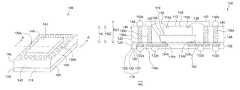
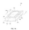
- FIG. 1A and FIG. 1Billustrate a wafer-level semiconductor device package 100 implemented in accordance with an embodiment of the invention.
- FIG. 1Aillustrates a perspective view of the package 100
- FIG. 1Billustrates a cross-sectional view of the package 100 , taken along line A-A of FIG. 1A .
- the package 100includes multiple semiconductor devices, namely a semiconductor device 102 and a semiconductor device 104 that is disposed adjacent to the semiconductor device 102 .
- the semiconductor devices 102 and 104are arranged in a stacked configuration within the package 100 , and are secured to one another in a suitable fashion, such as using a die attach film or an adhesive.
- a suitable fashionsuch as using a die attach film or an adhesive.
- stacking of the semiconductor devices 102 and 104 within the package 100achieves a higher density of semiconductor devices for a given footprint area taken up by the package 100 . While two semiconductor devices 102 and 104 are illustrated in FIG. 1B , it is contemplated that more or less semiconductor devices can be included for other implementations. In particular, it is contemplated that additional semiconductor devices can be included within the package 100 to achieve an even higher density of semiconductor devices.
- the semiconductor device 102includes an upper surface 108 , which is a back surface of the semiconductor device 102 , and a lower surface 106 , which is an active surface of the semiconductor device 102 that has contact pads 114 a and 114 b disposed adjacent thereto.
- the semiconductor device 104includes a lower surface 110 , which is a back surface of the semiconductor device 104 , and an upper surface 112 , which is an active surface of the semiconductor device 104 that has contact pads 116 a and 116 b disposed adjacent thereto.
- the contact pads 114 a and 114 bprovide input and output electrical connections for the semiconductor device 102
- the contact pads 116 a and 116 bprovide input and output electrical connections for the semiconductor device 104
- the semiconductor devices 102 and 104are stacked in a back-to-back configuration, such that their back surfaces face towards one another, while their active surfaces face away from one another.
- stacking of the semiconductor devices 102 and 104can be varied for other implementations.
- Each of the semiconductor devices 102 and 104is a semiconductor chip in the illustrated embodiment, although it is contemplated that the semiconductor devices 102 and 104 , in general, can be any active devices, any passive devices, or any combination thereof. As illustrated in FIG.
- the semiconductor device 102has a greater lateral extent relative to the semiconductor device 104 , although it is contemplated that the semiconductor device 102 can have a smaller lateral extent, or that the semiconductor devices 102 and 104 can have lateral extents that are substantially the same.
- the package 100also includes a redistribution unit 118 , which is disposed adjacent to the lower surface 106 of the semiconductor device 102 .
- the redistribution unit 118is electrically connected to the semiconductor devices 102 and 104 , and provides electrical pathways as well as mechanical stability and protection against environmental conditions.
- the redistribution unit 118includes a lower surface 120 , an upper surface 122 , and lateral surfaces 124 and 126 disposed adjacent to a periphery of the redistribution unit 118 and extending between the lower surface 120 and the upper surface 122 .
- each of the surfaces 120 , 122 , 124 , and 126is substantially planar, with the lateral surfaces 124 and 126 having a substantially orthogonal orientation with respect to the lower surface 120 or the upper surface 122 , although it is contemplated that the shapes and orientations of the surfaces 120 , 122 , 124 , and 126 can vary for other implementations.
- the periphery of the redistribution unit 118has a greater lateral extent relative to either of the semiconductor devices 102 and 104 , thereby allowing the package 100 to be implemented with a fan-out configuration, namely components of the package 100 can be disposed within as well as outside of an area defined by a periphery of the semiconductor device 102 or 104 .
- the redistribution unit 118is formed in situ during manufacturing as a set of redistribution layers, although it is contemplated that the redistribution unit 118 can include a preformed structure for other implementations.
- the redistribution unit 118is multi-layered and includes a pair of dielectric layers 128 and 130 and an electrically conductive layer 132 that is at least partially sandwiched by the dielectric layers 128 and 130 .
- each of the dielectric layers 128 and 130can be formed from a dielectric material that is polymeric or non-polymeric.
- the dielectric layers 128 and 130can be formed from polyimide, polybenzoxazole, benzocyclobutene, or a combination thereof.
- the dielectric layers 128 and 130can be formed from the same dielectric material or different dielectric materials.
- at least one of the dielectric layers 128 and 130can be formed from a dielectric material that is photoimageable or photoactive, thereby reducing manufacturing cost and time by allowing patterning using photolithography. While two dielectric layers 128 and 130 are illustrated in FIG. 1B , it is contemplated that more or less dielectric layers can be included for other implementations.
- the dielectric layer 128is formed with one set of openings that are aligned and sized so as to at least partially expose the contact pads 114 a and 114 b and allow electrical connection to the electrically conductive layer 132 , as well as another set of openings that are aligned and sized so as to at least partially expose the electrically conductive layer 132 adjacent to the upper surface 122 of the redistribution unit 118 and outside of the periphery of the semiconductor device 102 or 104 . Still referring to FIG.
- the dielectric layer 130is formed with openings that are aligned so as to at least partially expose the electrically conductive layer 132 adjacent to the lower surface 120 of the redistribution unit 118 , and that are sized so as to accommodate electrical contacts 132 a , 132 b , 132 c , and 132 d .
- the electrical contacts 132 a , 132 b , 132 c , and 132 dprovide input and output electrical connections for the package 100 , and at least a subset of the electrical contacts 132 a , 132 b , 132 c , and 132 d is electrically connected to the semiconductor devices 102 and 104 through the electrically conductive layer 132 .
- the electrical contacts 132 a , 132 b , 132 c , and 132 dare implemented as solder bumps, and, in accordance with the fan-out configuration of the package 100 , the electrical contacts 132 a , 132 b , 132 c , and 132 d are laterally disposed outside of the periphery of the semiconductor device 102 or 104 , although it is contemplated that the electrical contacts 132 a , 132 b , 132 c , and 132 d , in general, can be laterally disposed within that periphery, outside of that periphery, or both.
- the fan-out configuration of the package 100allows greater flexibility in terms of the arrangement and spacing of the electrical contacts 132 a , 132 b , 132 c , and 132 d , with reduced dependence upon the arrangement and spacing of the contact pads 114 a and 114 b of the semiconductor device 102 , as well as reduced dependence upon the arrangement and spacing of the contact pads 116 a and 116 b of the semiconductor device 104 .
- the electrically conductive layer 132serves as a redistribution network for the contact pads 114 a and 114 b of the semiconductor device 102 and the contact pads 116 a and 116 b of the semiconductor device 104 , and, in accordance with the fan-out configuration of the package 100 , the electrically conductive layer 132 extends laterally within the redistribution unit 118 and both within and outside of the periphery of the semiconductor device 102 or 104 . As illustrated in FIG.
- the electrically conductive layer 132includes an electrical interconnect 134 a , which is electrically connected to the electrical contact 132 a and is exposed adjacent to the upper surface 122 of the redistribution unit 118 , an electrical interconnect 134 b , which electrically connects the contact pads 114 a and 116 a to the electrical contact 132 b and is exposed adjacent to the upper surface 122 of the redistribution unit 118 , and an electrical interconnect 134 c , which electrically connects the contact pads 114 b and 116 b to the electrical contacts 132 c and 132 d and is exposed adjacent to the upper surface 122 of the redistribution unit 118 .
- each of the electrical interconnects 134 a , 134 b , and 134 ccan be formed from a metal, a metal alloy, a matrix with a metal or a metal alloy dispersed therein, or another suitable electrically conductive material.
- at least one of the electrical interconnects 134 a , 134 b , and 134 ccan be implemented as a set of vias and a set of electrical traces that are formed from aluminum, copper, titanium, or a combination thereof.
- the electrical interconnects 134 a , 134 b , and 134 ccan be formed from the same electrically conductive material or different electrically conductive materials. While one electrically conductive layer 132 is illustrated in FIG. 1B , it is contemplated that additional electrically conductive layers can be included for other implementations.
- the package 100also includes connecting elements 136 a , 136 b , 136 c , and 136 d that are disposed outside of the periphery of the semiconductor device 102 or 104 .
- the connecting elements 136 a , 136 b , 136 c , and 136 dextend upwardly from the electrically conductive layer 132 , and, in particular, the connecting element 136 a is electrically connected to and extends upwardly from the electrical interconnect 134 a , the connecting element 136 b is electrically connected to and extends upwardly from the electrical interconnect 134 b , and the connecting elements 136 c and 136 d are electrically connected to and extend upwardly from the electrical interconnect 134 c .
- the connecting elements 136 a , 136 b , 136 c , and 136 dare distributed in the form of rows, with each row extending along four sides of a substantially rectangular pattern or a substantially square-shaped pattern. More particularly, the rows include an outer row and an inner row, with the outer row including the connecting elements 136 a and 136 d , and with the inner row including the connecting elements 136 b and 136 c .
- connecting elements of the outer rowsuch as the connecting elements 136 a and 136 d
- connecting elements of the inner rowsuch as the connecting elements 136 b and 136 c
- connecting elements of the inner rowprovide electrical pathways within the package 100 and, in particular, between the semiconductor device 104 and other components of the package 100
- the provision of inter-package and intra-package electrical pathwaysalso can be combined within one or more of the connecting elements 136 a , 136 b , 136 c , and 136 d .
- the connecting elements 136 a , 136 b , 136 c , and 136 dextend the redistribution network provided by the electrically conductive layer 132 to three dimensions.
- the connecting elements 136 a , 136 b , 136 c , and 136 dfacilitate stacking of the semiconductor devices 102 and 104 within the package 100 as well as stacking of the package 100 and another package within a stacked package assembly, thereby achieving an even higher density of semiconductor devices for a given footprint area. While two rows of the connecting elements 136 a , 136 b , 136 c , and 136 d are illustrated in FIG.
- connecting elements 136 a , 136 b , 136 c , and 136 din general, can be distributed in any one-dimensional pattern or any two-dimensional pattern.
- the connecting elements 136 a , 136 b , 136 c , and 136 dare implemented as elongated structures and, more particularly, as elongated, electrically conductive structures that are disposed within and at least partially fill respective through-holes formed in accordance with manufacturing operations further described below.
- the connecting elements 136 a , 136 b , 136 c , and 136 dare fouled from a metal, a metal alloy, a matrix with a metal or a metal alloy dispersed therein, or another suitable electrically conductive material.
- at least one of the connecting elements 136 a , 136 b , 136 c , and 136 dcan be formed from copper or a copper alloy.
- a size of each connecting element 136 a , 136 b , 136 c , or 136 dcan be specified in accordance with a height H C of the connecting element 136 a , 136 b , 136 c , or 136 d , namely a vertical extent of the connecting element 136 a , 136 b , 136 c , or 136 d , and a width W C of the connecting element 136 a , 136 b , 136 c , or 136 d , namely a lateral extent of the connecting element 136 a , 136 b , 136 c , or 136 d .
- the width W Ccan correspond to, for example, an average of lateral extents along a set of orthogonal directions.
- each connecting element 136 a , 136 b , 136 c , or 136 dcan be in the range of about 100 micrometer (“ ⁇ m”) to about 700 ⁇ m, such as from about 150 ⁇ m to about 650 ⁇ m or from about 200 ⁇ m to about 600 ⁇ m, and the width W C of each connecting element 136 a , 136 b , 136 c , or 136 d can be in the range of about 100 ⁇ m to about 500 ⁇ m, such as from about 150 ⁇ m to about 450 ⁇ m or from about 200 ⁇ m to about 400 ⁇ m.
- each connecting element 136 a , 136 b , 136 c , or 136 dis substantially aligned or co-planar with the upper surface 112 of the semiconductor device 104
- a lower end of each connecting element 136 a , 136 b , 136 c , or 136 dis substantially aligned or co-planar with the lower surface 106 of the semiconductor device 102
- the height H C of each connecting element 136 a , 136 b , 136 c , or 136 dis substantially the same as combined vertical extents of the semiconductor devices 102 and 104 in their stacked configuration.
- the vertical extents of the connecting elements 136 a , 136 b , 136 c , and 136 d and their alignment with the upper surface 112 and the lower surface 106can be varied for other implementations.
- the semiconductor device 104is wire-bonded to the connecting elements 136 b and 136 c (and other inner row connecting elements) via a set of wires 138 , which electrically connect the contact pads 116 a and 116 b to respective upper ends of the connecting elements 136 b and 136 c .
- the wires 138are formed from gold, copper, or another suitable electrically conductive material.
- the wires 138is desirably formed from copper, since, as compared to gold, copper has a superior electrical conductivity and a lower cost, while allowing the wires 138 to be formed with reduced diameters.
- the wires 138can be coated with a suitable metal, such as palladium, as a protection against oxidation and other environmental conditions.
- the use of wire-bondingfacilitates stacking functionality of the package 100 , including stacking of the semiconductor devices 102 and 104 within the package 100 , without requiring the formation of another redistribution unit to provide electrical pathways, thereby reducing manufacturing cost and time.
- the use of wire-bondingcan more readily accommodate certain types of semiconductor devices, such as wire-bond chips that are specifically designed for wire-bonding.
- the package 100also includes a package body 140 that is disposed adjacent to the upper surface 122 of the redistribution unit 118 .
- the package body 140substantially covers or encapsulates the semiconductor devices 102 and 104 , the wires 138 , and the connecting elements 136 b and 136 c (and other inner row connecting elements) to provide structural rigidity as well as protection against environmental conditions.
- the package body 140extends to sides of the redistribution unit 118 and covers or encapsulates the connecting elements 136 a and 136 d (and other outer row connecting elements), while at least partially exposing upper ends of the connecting elements 136 a and 136 d to allow stacking another package on top of the package 100 .
- the package body 140is formed from a molding material, and includes a central upper surface 142 , a peripheral upper surface 144 , and lateral surfaces 146 and 148 , which are disposed adjacent to sides of the package body 140 .
- each of the central upper surface 142 and the peripheral upper surface 144is substantially planar and has a substantially parallel orientation with respect to the lower surface 120 or the upper surface 122 of the redistribution unit 118 , although it is contemplated that the shapes and orientations of the upper surfaces 142 and 144 can vary for other implementations. Referring to FIG. 1A and FIG.
- the package body 140has a greater thickness adjacent to a central portion of the package body 140 so as to substantially cover the semiconductor devices 102 and 104 , the wires 138 , and the connecting elements 136 b and 136 c , while the package body 140 has a reduced thickness adjacent to a peripheral portion of the package body 140 so as to at least partially expose the connecting elements 136 a and 136 d , with their upper ends substantially aligned or co-planar with the peripheral upper surface 144 .
- a central thickness H P1 of the package body 140namely a vertical distance between the central upper surface 142 of the package body 140 and the upper surface 122 of the redistribution unit 118
- a peripheral thickness H P2 of the package body 140namely a vertical distance between the peripheral upper surface 144 of the package body 140 and the upper surface 122 of the redistribution unit 118 , which, in turn, is substantially the same as the height H C of each connecting element 136 a , 136 b , 136 c , or 136 d .
- the peripheral thickness H P2can be no greater than about 9/10 of the central thickness H P1 , such as from about 1 ⁇ 2 to about 9/10 of H P1 or from about 2 ⁇ 3 to about 9/10 of H P1 .
- the central thickness H P1can be in the range of about 200 ⁇ m to about 800 ⁇ m, such as from about 250 ⁇ m to about 750 ⁇ m or from about 300 ⁇ m to about 700 ⁇ m
- the peripheral thickness H P2can be in the range of about 100 ⁇ m to about 700 ⁇ m, such as from about 150 ⁇ m to about 650 ⁇ m or from about 200 ⁇ m to about 600 ⁇ m.
- connecting elements 136 a and 136 dare illustrated as substantially aligned with the peripheral upper surface 144 , it is also contemplated that the upper ends of the connecting elements 136 a and 136 d can be recessed below or can protrude above the peripheral upper surface 144 .
- the lateral surfaces 146 and 148 of the package body 140are substantially planar and have a substantially orthogonal orientation with respect to the lower surface 120 or the upper surface 122 of the redistribution unit 118 , although it is contemplated that the shapes and orientations of the lateral surfaces 146 and 148 can vary for other implementations. Also, the lateral surfaces 146 and 148 are substantially aligned or co-planar with the lateral surfaces 124 and 126 of the redistribution unit 118 , respectively, such that, in conjunction with the lateral surfaces 124 and 126 , the lateral surfaces 146 and 148 define sides of the package 100 .
- this alignmentis accomplished such that the package body 140 has a lateral extent that substantially corresponds to that of the redistribution unit 118 , albeit with a reduced thickness adjacent to the sides of the package 100 .
- the alignment of the lateral surfaces 124 , 126 , 146 , and 148can be varied from that illustrated in FIG. 1A and FIG. 1B .
- electrical contacts 150 a and 150 bDisposed adjacent to the peripheral upper surface 144 of the package body 140 are electrical contacts, including electrical contacts 150 a and 150 b , which are electrically connected to and extend upwardly from respective upper ends of the connecting elements 136 a and 136 d (and other outer row connecting elements).
- the electrical contacts 150 a and 150 bserve as pre-solders for stacking another package on top of the package 100 , and, like the connecting elements 136 a and 136 d , the electrical contacts 150 a and 150 b are distributed in the form of a row extending along four sides of a substantially rectangular pattern or a substantially square-shaped pattern.
- the electrical contacts 150 a and 150 bare implemented as solder bumps, and, in accordance with the fan-out configuration of the package 100 , the electrical contacts 150 a and 150 b are laterally disposed outside of the periphery of the semiconductor device 102 or 104 , although it is contemplated that the electrical contacts 150 a and 150 b , in general, can be laterally disposed within that periphery, outside of that periphery, or both.
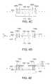
- FIG. 2A and FIG. 2Billustrate enlarged, cross-sectional views of a portion of the package 100 of FIG. 1A and FIG. 1B , with certain details omitted for ease of presentation.
- FIG. 2Aillustrates one particular implementation of the connecting element 136 b
- FIG. 2Billustrates another particular implementation of the connecting element 136 b
- While the following featuresare described with reference to the connecting element 136 b , it is contemplated that these features can similarly apply to other connecting elements of the package 100 .
- the connecting element 136 bis implemented as a solid, elongated structure and, more particularly, as an electrically conductive pillar or post 200 that is disposed within and substantially fills a through-hole defined by the package body 140 .
- An upper end of the electrically conductive post 200includes a connection surface to which the wire 138 is electrically connected.
- this connection surfacecan be formed by subjecting the upper end of the electrically conductive post 200 to a set of surface finishing operations, which yield a set of layers to enhance reliability of electrical connections to the wire 138 .
- surface finishing layersinclude those based on gold, such as direct immersion gold, electroless nickel/immersion gold, and electroless nickel/electroless palladium/immersion gold.
- the connecting element 136 bis implemented as a hollow, elongated structure and, more particularly, as an electrically conductive channel 202 that is disposed within and partially fills a through-hole defined by the package body 140 .
- a molding material forming the package body 140can fill a remaining portion of the through-hole, although it is contemplated that another suitable filler material can be used, or that the through-hole can remain at least partially hollow.
- An upper end of the electrically conductive channel 202has a greater lateral extent and is implemented as a contact pad 204 , which includes a connection surface to which the wire 138 is electrically connected. During manufacturing, this connection surface can be formed by subjecting the contact pad 204 to a set of surface finishing operations similar to those described above with reference to FIG. 2A .
- FIG. 3illustrates a cross-sectional view of a stacked package assembly 300 implemented in accordance with an embodiment of the invention, with certain details omitted for ease of presentation.
- FIG. 3illustrates a particular implementation of the assembly 300 that is formed using the package 100 of FIG. 1A through FIG. 2B .
- the assembly 300includes a semiconductor device package 302 , which corresponds to a top package that is disposed above and electrically connected to the package 100 that corresponds to a bottom package.
- the package 302is implemented as a ball grid array (“BGA”) package, although it is contemplated that a number of other package types can be used, including a land grid array (“LGA”) package, a quad flat no-lead (“QFN”) package, an advanced QFN (“aQFN”) package, and other types of BGA package, such as a window BGA package. While two stacked packages 100 and 302 are illustrated in FIG. 3 , it is contemplated that additional packages can be included for other implementations. Certain aspects of the package 302 can be implemented in a similar fashion as previously described for the package 100 and, thus, are not further described herein.
- the package 302includes electrical contacts, including electrical contacts 304 a and 304 b , which provide input and output electrical connections for the package 302 and extend downwardly from a lower surface of the package 302 .
- the electrical contacts 304 a and 304 bare implemented as solder bumps, and, like the electrical contacts 150 a and 150 b , the electrical contacts 304 a and 304 b are distributed in the form of a row extending along four sides of a substantially rectangular pattern or a substantially square-shaped pattern.
- the electrical contacts 304 a and 304 b of the package 302are reflowed and undergo metallurgical bonding with the electrical contacts 150 a and 150 b of the package 100 .
- the electrical contacts 304 a and 304 bfuse or merge with respective ones of the electrical contacts 150 a and 150 b to provide electrical pathways between the packages 100 and 302 .
- FIG. 4A through FIG. 4Hillustrate a manufacturing method of forming a wafer-level semiconductor device package, according to an embodiment of the invention.
- the following manufacturing operationsare described with reference to the package 100 of FIG. 1A through FIG. 2B .
- the manufacturing operationscan be similarly carried out to form other semiconductor device packages.
- a carrier 400is provided, and multiple pairs of semiconductor devices are disposed adjacent to the carrier 400 in a stacked configuration, including the semiconductor devices 102 and 104 .
- the semiconductor devices 102 and 104are stacked in a back-to-back configuration, with the active surface 112 of the semiconductor device 104 facing the carrier 400 , and with the active surface 106 of the semiconductor device 102 facing away from the carrier 400 .
- Stacked pairs of semiconductor devicescan be arranged on the carrier 400 in an array manner, in which the stacked pairs of semiconductor devices are arranged in a two-dimensional fashion, or in a strip manner, in which the stacked pairs of semiconductor devices are arranged sequentially in a linear fashion.
- the semiconductor device 102 or 104is initially included within a wafer at an initial spacing with respect to neighboring semiconductor devices, and the wafer is subjected to singulation to separate the semiconductor device 102 or 104 from the neighboring semiconductor devices.
- stacked pairs of semiconductor devicesare arranged so as to have a greater nearest-neighbor spacing with respect to one another, relative to an initial nearest-neighbor spacing within a wafer, thereby facilitating a fan-out configuration of resulting packages.
- the following manufacturing operationsare primarily described with reference to the semiconductor devices 102 and 104 and related components, although the manufacturing operations can be similarly carried for other stacked pairs of semiconductor devices in a parallel fashion or sequentially.
- a molding material 402is applied to the carrier 400 so as to cover or encapsulate the semiconductor devices 102 and 104 , while the active surfaces 106 and 112 of the semiconductor devices 102 and 104 remain at least partially exposed. Because the semiconductor device 104 is arranged with its active surface 112 facing the carrier 400 , sides of the semiconductor device 104 are substantially covered by the molding material 402 , while its active surface 112 is substantially uncovered by the molding material 402 . Also, by positioning a molding plate or other molding structure adjacent to the active surface 106 of the semiconductor device 102 , sides of the semiconductor device 102 are substantially covered by the molding material 402 , while its active surface 106 is substantially uncovered by the molding material 402 .
- the molding material 402can include, for example, a Novolac-based resin, an epoxy-based resin, a silicone-based resin, or another suitable encapsulant. Suitable fillers also can be included, such as powdered SiO 2 .
- the molding material 402can be applied using any of a number of molding techniques, such as compression molding, injection molding, or transfer molding. Once applied, the molding material 402 is hardened or solidified, such as by lowering the temperature to below a melting point of the molding material 402 , thereby forming a molded structure 404 . Referring to FIG.
- the resulting molded structure 404includes a front surface 408 that is substantially aligned or co-planar with the active surface 106 of the semiconductor device 102 , and an opposite, back surface 410 that is substantially aligned or co-planar with the active surface 112 of the semiconductor device 104 .
- a thickness of the molded structure 404is substantially the same as the combined vertical extents of the semiconductor devices 102 and 104 in their stacked configuration.
- the molded structure 404 along with the encapsulated semiconductor devices 102 and 104can be referred to as a reconstituted wafer.
- multiple through-holesare formed in the molded structure 404 , including through-holes 406 a , 406 b , 406 c , and 406 d that are distributed in the form of an outer row and an inner row surrounding the semiconductor devices 102 and 104 , with each row extending along four sides of a substantially rectangular pattern or a substantially square-shaped pattern.
- the through-holes 406 a , 406 b , 406 c , and 406 dcan be formed in any of a number of ways, such as chemical etching, laser drilling, or mechanical drilling to form openings.
- laser drillingcan be carried out using a green laser, an infrared laser, a solid-state laser, or a CO 2 laser, which applies a laser beam in a pulsed fashion or a continuous wave fashion.
- each of the through-holes 406 a , 406 b , 406 c , and 406 dhas a lateral boundary that is shaped in the form of a circular cylinder, including a substantially circular cross-section.
- the shapes of the through-holes 406 a , 406 b , 406 c , and 406 din general, can be any of a number of shapes, such as another type of cylindrical shape, such as an elliptic cylindrical shape, a square cylindrical shape, or a rectangular cylindrical shape, or a non-cylindrical shape, such as a cone, a funnel, or another tapered shape.
- the lateral boundaries of the through-holes 406 a , 406 b , 406 c , and 406 dcan be curved or roughly textured.
- each of the through-holes 406 a , 406 b , 406 c , and 406 dvertically extends through substantially the entire thickness of the molded structure 404 , namely so as to substantially span a vertical distance between the active surfaces 106 and 112 of the semiconductor devices 102 and 104 .
- the vertical extents of the through-holes 406 a , 406 b , 406 c , and 406 dcan be varied for other implementations.
- suitable selection and control over operating parameters of a laserallow control over sizes and shapes of the through-holes 406 a , 406 b , 406 c , and 406 d.
- an electrically conductive material 418is applied to and drawn into the through-holes 406 a , 406 b , 406 c , and 406 d so as to at least partially fill the through-holes 406 a , 406 b , 406 c , and 406 d , thereby forming the connecting elements 136 a , 136 b , 136 c , and 136 d as illustrated in FIG. 4D .
- the electrically conductive material 418includes a metal, a metal alloy, a matrix with a metal or a metal alloy dispersed therein, or another suitable electrically conductive material.
- the electrically conductive material 418can include a metal, such as copper, a solder, such as any of a number of fusible metal alloys having melting points in the range of about 90° C. to about 450° C., or an electrically conductive adhesive or paste, such as any of a number of resins having an electrically conductive filler dispersed therein.
- suitable soldersinclude tin-lead alloys, copper-zinc alloys, copper-silver alloys, tin-silver-copper alloys, bismuth-containing alloys, indium-containing alloys, and antimony-containing alloys
- suitable adhesivesinclude epoxy-based resins and silicone-based resins having silver fillers or carbon fillers.
- the electrically conductive material 418can be applied in any of a number of ways, such as electroless plating, electrolytic plating, or by using a dispenser.
- each of the resulting connecting elements 136 a , 136 b , 136 c , and 136 dincludes one end that is substantially aligned or co-planar with the front surface 408 of the molded structure 404 (and with the active surface 106 of the semiconductor device 102 ), and an opposite end that is substantially aligned or co-planar with the back surface 410 of the molded structure 404 (and with the active surface 112 of the semiconductor device 104 ).
- the height H C of each connecting element 136 a , 136 b , 136 c , or 136 dis substantially the same as the thickness of the molded structure 404 .
- the vertical extents of the connecting elements 136 a , 136 b , 136 c , and 136 d and their alignment with the surfaces 408 and 410can be varied for other implementations.
- a set of redistribution layersare next formed in situ adjacent to the front surface 408 of the molded structure 404 and the active surface 106 of the semiconductor device 102 , thereby forming the redistribution unit 118 as illustrated in FIG. 4E .
- the redistribution unit 118includes the pair of dielectric layers 128 and 130 and the electrically conductive layer 132 that is at least partially sandwiched by the dielectric layers 128 and 130 .
- Each of the dielectric layers 128 and 130is formed by applying a dielectric material using any of a number of coating techniques, such as printing, spinning, or spraying, in conjunction with patterning to form suitably sized and aligned openings.
- an electrically conductive materialis applied using any of a number of coating techniques, such as chemical vapor deposition, electroless plating, electrolytic plating, printing, spinning, spraying, sputtering, or vacuum deposition, in conjunction with patterning to form the electrically conductive layer 132 .
- Patterning of the dielectric layers 128 and 130 and the electrically conductive layer 132can be carried out in any of a number of ways, such as photolithography, chemical etching, laser drilling, or mechanical drilling.
- the electrical contacts 132 a , 132 b , 132 c , and 132 dare formed and are accommodated by openings defined by the dielectric layer 130 , such as by applying a solder and reflowing and solidifying that solder to form solder bumps.
- the molded structure 404 along with various encapsulated componentsare separated from the carrier 400 , and are reoriented to an upright orientation as illustrated in FIG. 4F .
- the semiconductor device 104is then wire-bonded to the connecting elements 136 b and 136 c (and other inner row connecting elements) via the wires 138 .
- a set of surface finishing operationscan be carried out prior to, or in conjunction with, wire-bonding to enhance reliability of electrical connections.
- the use of wire-bondingprovides electrical pathways that allow stacking of the semiconductor devices 102 and 104 , without requiring the formation of another redistribution unit adjacent to the back surface 410 of the molded structure 404 and the active surface 112 of the semiconductor device 104 .
- a molding material 412is then selectively applied to a central portion of the molded structure 404 so as to substantially cover or encapsulate the active surface 112 of the semiconductor device 104 , the wires 138 , and upper ends of the connecting elements 136 b and 136 c (and other inner row connecting elements).
- the molding material 412can be the same as, or different from, the molding material 402 previously described with reference to FIG. 4B , and can be applied using any of a number of molding techniques, such as compression molding, injection molding, or transfer molding. Once applied, the molding material 412 is hardened or solidified, such as by lowering the temperature to below a melting point of the molding material 412 , thereby forming the package body 140 .
- the package body 140has a reduced thickness adjacent to the sides of the package body 140 , adjacent to which upper ends of the connecting elements 136 a and 136 d (and other outer row connecting elements) are exposed. It is also contemplated that the package body 140 can be formed by applying the molding material 412 so as to have a substantially uniform thickness, followed by a thickness-reduction operation, such as chemical etching; laser drilling; mechanical cutting, drilling, routing, or grinding; or another removal technique to yield a varying thickness profile.
- a thickness-reduction operationsuch as chemical etching; laser drilling; mechanical cutting, drilling, routing, or grinding; or another removal technique to yield a varying thickness profile.
- the electrical contacts 150 a and 150 bare formed and are disposed adjacent to upper ends of the connecting elements 136 a and 136 d , such as by applying a solder and reflowing and solidifying that solder to form solder bumps, thereby resulting in the package 100 .
- a set of singulation operationscan be carried out to separate the package 100 from neighboring packages.
Landscapes
- Engineering & Computer Science (AREA)
- Microelectronics & Electronic Packaging (AREA)
- Power Engineering (AREA)
- Computer Hardware Design (AREA)
- Physics & Mathematics (AREA)
- Condensed Matter Physics & Semiconductors (AREA)
- General Physics & Mathematics (AREA)
- Manufacturing & Machinery (AREA)
- Structures Or Materials For Encapsulating Or Coating Semiconductor Devices Or Solid State Devices (AREA)
- Container, Conveyance, Adherence, Positioning, Of Wafer (AREA)
- Production Of Multi-Layered Print Wiring Board (AREA)
Abstract
Description
The invention relates generally to semiconductor device packages. More particularly, the invention relates to wafer-level semiconductor device packages with stacking functionality.
Semiconductor devices have become progressively more complex, driven at least in part by the demand for smaller sizes and enhanced functionality. While the benefits of smaller sizes and enhanced functionality are apparent, these characteristics of semiconductor devices also can create problems.
In conventional wafer-level packaging, semiconductor devices within a wafer are packaged prior to singulation of the wafer. As such, conventional wafer-level packaging can be restricted to a fan-in configuration, namely electrical contacts and other components of a resulting semiconductor device package are restricted to an area defined by a periphery of a semiconductor device. Any component disposed outside of the periphery of the semiconductor device typically is not supported and typically is removed upon singulation. The restriction of a fan-in configuration presents challenges as device sizes continue to shrink, while device functionality continues to increase.
In conjunction, electronic products typically have to accommodate a high density of semiconductor devices in a limited space. For example, the space available for processors, memory devices, and other active or passive devices can be rather limited in cell phones, personal digital assistants, laptop computers, and other portable consumer products. Packaging of semiconductor devices within semiconductor device packages can take up additional valuable space within electronic products. As such, there is a strong trend towards increasing a density of semiconductor devices for a given footprint area taken up by a semiconductor device package. Unfortunately, conventional wafer-level packaging can be inadequate with respect to addressing this trend.
It is against this background that a need arose to develop the wafer-level semiconductor device packages and related stacked package assemblies and methods described herein.
One aspect of the invention relates to wafer-level semiconductor device packages with stacking functionality and related stacked package assemblies. In one embodiment, a semiconductor device package includes: (1) a redistribution unit including an upper surface; (2) a set of stacked semiconductor devices including: (a) a first semiconductor device disposed adjacent to the redistribution unit and including a first active surface that faces the upper surface of the redistribution unit, and (b) a second semiconductor device disposed adjacent to the first semiconductor device and including a second active surface that faces away from the first active surface; (3) a set of connecting elements disposed adjacent to a periphery of the set of stacked semiconductor devices and each extending upwardly from the upper surface of the redistribution unit, the set of connecting elements including: (a) a first connecting element including a first upper end, and (b) a second connecting element including a second upper end that is wire-bonded to the second active surface of the second semiconductor device; and (4) a package body disposed adjacent to the upper surface of the redistribution unit and covering the set of stacked semiconductor devices and the set of connecting elements, the package body including a central upper surface and a peripheral upper surface, the central upper surface of the package body being spaced above the second active surface of the second semiconductor device, the first upper end of the first connecting element being exposed adjacent to the peripheral upper surface of the package body.
Another aspect of the invention relates to manufacturing methods of forming wafer-level semiconductor device packages with stacking functionality. In one embodiment, a manufacturing method includes: (1) providing a first semiconductor device and a second semiconductor device, the first semiconductor device including a first active surface, the second semiconductor device including a second active surface; (2) stacking the first semiconductor device and the second semiconductor device, such that the first active surface and the second active surface face away from one another; (3) applying a first molding material to form a molded structure covering sides of the first semiconductor device and the second semiconductor device, the molded structure including a front surface and an opposite, back surface, the first active surface of the first semiconductor device being at least partially exposed adjacent to the front surface of the molded structure, the second active surface of the second semiconductor device being at least partially exposed adjacent to the back surface of the molded structure; (4) forming a set of through-holes extending between the front surface and the back surface of the molded structure and surrounding the first semiconductor device and the second semiconductor device; (5) applying an electrically conductive material to the set of through-holes to form a set of connecting elements; (6) forming a redistribution unit adjacent to the first active surface of the first semiconductor device and the front surface of the molded structure; (7) electrically connecting, via a set of wires, the second active surface of the second semiconductor device to at least one of the set of connecting elements; and (8) applying a second molding material adjacent to the second active surface of the second semiconductor device and the back surface of the molded structure to form a package body, the package body including a central portion and a peripheral portion, the central portion having a central thickness Hp so as to cover the second active surface of the second semiconductor device and the set of wires, the peripheral portion having a peripheral thickness HP2so as to at least partially expose one end of at least one of the set of connecting elements.
Other aspects and embodiments of the invention are also contemplated. The foregoing summary and the following detailed description are not meant to restrict the invention to any particular embodiment but are merely meant to describe some embodiments of the invention.
For a better understanding of the nature and objects of some embodiments of the invention, reference should be made to the following detailed description taken in conjunction with the accompanying drawings. In the drawings, like reference numbers denote like elements, unless the context clearly dictates otherwise.
The following definitions apply to some of the aspects described with respect to some embodiments of the invention. These definitions may likewise be expanded upon herein.
As used herein, the singular terms “a,” “an,” and “the” include plural referents unless the context clearly dictates otherwise. Thus, for example, reference to a connecting element can include multiple connecting elements unless the context clearly dictates otherwise.
As used herein, the term “set” refers to a collection of one or more components. Thus, for example, a set of layers can include a single layer or multiple layers. Components of a set also can be referred to as members of the set. Components of a set can be the same or different. In some instances, components of a set can share one or more common characteristics.
As used herein, the term “adjacent” refers to being near or adjoining. Adjacent components can be spaced apart from one another or can be in actual or direct contact with one another. In some instances, adjacent components can be connected to one another or can be formed integrally with one another.
As used herein, relative terms, such as “inner,” “interior,” “outer,” “exterior,” “top,” “bottom,” “front,” “back,” “upper,” “upwardly,” “lower,” “downwardly,” “vertical,” “vertically,” “lateral,” “laterally,” “above,” and “below,” refer to an orientation of a set of components with respect to one another, such as in accordance with the drawings, but do not require a particular orientation of those components during manufacturing or use.
As used herein, the terms “connect,” “connected,” and “connection” refer to an operational coupling or linking. Connected components can be directly coupled to one another or can be indirectly coupled to one another, such as through another set of components.
As used herein, the terms “substantially” and “substantial” refer to a considerable degree or extent. When used in conjunction with an event or circumstance, the terms can refer to instances in which the event or circumstance occurs precisely as well as instances in which the event or circumstance occurs to a close approximation, such as accounting for typical tolerance levels of the manufacturing operations described herein.
As used herein, the terms “electrically conductive” and “electrical conductivity” refer to an ability to transport an electric current. Electrically conductive materials typically correspond to those materials that exhibit little or no opposition to flow of an electric current. One measure of electrical conductivity is in terms of Siemens per meter (“S·m−1”). Typically, an electrically conductive material is one having a conductivity greater than about 104S·m−1, such as at least about 105S·m−1or at least about 106S·m−1. Electrical conductivity of a material can sometimes vary with temperature. Unless otherwise specified, electrical conductivity of a material is defined at room temperature.
Attention first turns toFIG. 1A andFIG. 1B , which illustrate a wafer-levelsemiconductor device package 100 implemented in accordance with an embodiment of the invention. In particular,FIG. 1A illustrates a perspective view of thepackage 100, whileFIG. 1B illustrates a cross-sectional view of thepackage 100, taken along line A-A ofFIG. 1A .
Referring toFIG. 1B , thepackage 100 includes multiple semiconductor devices, namely asemiconductor device 102 and asemiconductor device 104 that is disposed adjacent to thesemiconductor device 102. In the illustrated embodiment, thesemiconductor devices package 100, and are secured to one another in a suitable fashion, such as using a die attach film or an adhesive. Advantageously, such stacking of thesemiconductor devices package 100 achieves a higher density of semiconductor devices for a given footprint area taken up by thepackage 100. While twosemiconductor devices FIG. 1B , it is contemplated that more or less semiconductor devices can be included for other implementations. In particular, it is contemplated that additional semiconductor devices can be included within thepackage 100 to achieve an even higher density of semiconductor devices.
As illustrated inFIG. 1B , thesemiconductor device 102 includes an upper surface108, which is a back surface of thesemiconductor device 102, and alower surface 106, which is an active surface of thesemiconductor device 102 that hascontact pads semiconductor device 104 includes alower surface 110, which is a back surface of thesemiconductor device 104, and anupper surface 112, which is an active surface of thesemiconductor device 104 that hascontact pads contact pads semiconductor device 102, while thecontact pads semiconductor device 104. In the illustrated embodiment, thesemiconductor devices semiconductor devices semiconductor devices semiconductor devices FIG. 1B , thesemiconductor device 102 has a greater lateral extent relative to thesemiconductor device 104, although it is contemplated that thesemiconductor device 102 can have a smaller lateral extent, or that thesemiconductor devices
Referring toFIG. 1A andFIG. 1B , thepackage 100 also includes aredistribution unit 118, which is disposed adjacent to thelower surface 106 of thesemiconductor device 102. Theredistribution unit 118 is electrically connected to thesemiconductor devices FIG. 1A andFIG. 1B , theredistribution unit 118 includes alower surface 120, anupper surface 122, andlateral surfaces redistribution unit 118 and extending between thelower surface 120 and theupper surface 122. In the illustrated embodiment, each of thesurfaces lateral surfaces lower surface 120 or theupper surface 122, although it is contemplated that the shapes and orientations of thesurfaces redistribution unit 118, as defined by the lateral surfaces124 and126, has a greater lateral extent relative to either of thesemiconductor devices package 100 to be implemented with a fan-out configuration, namely components of thepackage 100 can be disposed within as well as outside of an area defined by a periphery of thesemiconductor device
In the illustrated embodiment, theredistribution unit 118 is formed in situ during manufacturing as a set of redistribution layers, although it is contemplated that theredistribution unit 118 can include a preformed structure for other implementations. Referring toFIG. 1B , theredistribution unit 118 is multi-layered and includes a pair ofdielectric layers conductive layer 132 that is at least partially sandwiched by thedielectric layers dielectric layers dielectric layers dielectric layers dielectric layers dielectric layers FIG. 1B , it is contemplated that more or less dielectric layers can be included for other implementations.
As illustrated inFIG. 1B , thedielectric layer 128 is formed with one set of openings that are aligned and sized so as to at least partially expose thecontact pads conductive layer 132, as well as another set of openings that are aligned and sized so as to at least partially expose the electricallyconductive layer 132 adjacent to theupper surface 122 of theredistribution unit 118 and outside of the periphery of thesemiconductor device FIG. 1B , thedielectric layer 130 is formed with openings that are aligned so as to at least partially expose the electricallyconductive layer 132 adjacent to thelower surface 120 of theredistribution unit 118, and that are sized so as to accommodateelectrical contacts electrical contacts package 100, and at least a subset of theelectrical contacts semiconductor devices conductive layer 132. In the illustrated embodiment, theelectrical contacts package 100, theelectrical contacts semiconductor device electrical contacts package 100 allows greater flexibility in terms of the arrangement and spacing of theelectrical contacts contact pads semiconductor device 102, as well as reduced dependence upon the arrangement and spacing of thecontact pads semiconductor device 104.
The electricallyconductive layer 132 serves as a redistribution network for thecontact pads semiconductor device 102 and thecontact pads semiconductor device 104, and, in accordance with the fan-out configuration of thepackage 100, the electricallyconductive layer 132 extends laterally within theredistribution unit 118 and both within and outside of the periphery of thesemiconductor device FIG. 1B , the electricallyconductive layer 132 includes anelectrical interconnect 134a, which is electrically connected to theelectrical contact 132aand is exposed adjacent to theupper surface 122 of theredistribution unit 118, anelectrical interconnect 134b, which electrically connects thecontact pads electrical contact 132band is exposed adjacent to theupper surface 122 of theredistribution unit 118, and anelectrical interconnect 134c, which electrically connects thecontact pads electrical contacts upper surface 122 of theredistribution unit 118. In general, each of theelectrical interconnects electrical interconnects electrical interconnects conductive layer 132 is illustrated inFIG. 1B , it is contemplated that additional electrically conductive layers can be included for other implementations.
As illustrated inFIG. 1B , thepackage 100 also includes connectingelements semiconductor device elements conductive layer 132, and, in particular, the connectingelement 136ais electrically connected to and extends upwardly from theelectrical interconnect 134a, the connectingelement 136bis electrically connected to and extends upwardly from theelectrical interconnect 134b, and the connectingelements electrical interconnect 134c. Referring toFIG. 1A andFIG. 1B , the connectingelements elements elements elements package 100 and another package within a stacked package assembly, and connecting elements of the inner row, such as the connectingelements package 100 and, in particular, between thesemiconductor device 104 and other components of thepackage 100. However, it is contemplated that the provision of inter-package and intra-package electrical pathways also can be combined within one or more of the connectingelements elements conductive layer 132 to three dimensions. In such manner, the connectingelements semiconductor devices package 100 as well as stacking of thepackage 100 and another package within a stacked package assembly, thereby achieving an even higher density of semiconductor devices for a given footprint area. While two rows of the connectingelements FIG. 1B , it is contemplated that more or less rows of connecting elements can be included for other implementations, and that the connectingelements
In the illustrated embodiment, the connectingelements elements elements FIG. 1B , a size of each connectingelement element element element element element element element
Still referring toFIG. 1B , an upper end of each connectingelement upper surface 112 of thesemiconductor device 104, while a lower end of each connectingelement lower surface 106 of thesemiconductor device 102. Stated in another way, the height HCof each connectingelement semiconductor devices elements upper surface 112 and thelower surface 106 can be varied for other implementations. As illustrated inFIG. 1B , thesemiconductor device 104 is wire-bonded to the connectingelements wires 138, which electrically connect thecontact pads elements wires 138 are formed from gold, copper, or another suitable electrically conductive material. For certain implementations, at least a subset of thewires 138 is desirably formed from copper, since, as compared to gold, copper has a superior electrical conductivity and a lower cost, while allowing thewires 138 to be formed with reduced diameters. Thewires 138 can be coated with a suitable metal, such as palladium, as a protection against oxidation and other environmental conditions. Advantageously, the use of wire-bonding facilitates stacking functionality of thepackage 100, including stacking of thesemiconductor devices package 100, without requiring the formation of another redistribution unit to provide electrical pathways, thereby reducing manufacturing cost and time. In addition, the use of wire-bonding can more readily accommodate certain types of semiconductor devices, such as wire-bond chips that are specifically designed for wire-bonding.
Referring toFIG. 1A andFIG. 1B , thepackage 100 also includes apackage body 140 that is disposed adjacent to theupper surface 122 of theredistribution unit 118. In conjunction with theredistribution unit 118, thepackage body 140 substantially covers or encapsulates thesemiconductor devices wires 138, and the connectingelements package body 140 extends to sides of theredistribution unit 118 and covers or encapsulates the connectingelements elements package 100.
Thepackage body 140 is formed from a molding material, and includes a centralupper surface 142, a peripheralupper surface 144, andlateral surfaces package body 140. In the illustrated embodiment, each of the centralupper surface 142 and the peripheralupper surface 144 is substantially planar and has a substantially parallel orientation with respect to thelower surface 120 or theupper surface 122 of theredistribution unit 118, although it is contemplated that the shapes and orientations of theupper surfaces FIG. 1A andFIG. 1B , thepackage body 140 has a greater thickness adjacent to a central portion of thepackage body 140 so as to substantially cover thesemiconductor devices wires 138, and the connectingelements package body 140 has a reduced thickness adjacent to a peripheral portion of thepackage body 140 so as to at least partially expose the connectingelements upper surface 144. In particular, a central thickness HP1of thepackage body 140, namely a vertical distance between the centralupper surface 142 of thepackage body 140 and theupper surface 122 of theredistribution unit 118, is greater than a peripheral thickness HP2of thepackage body 140, namely a vertical distance between the peripheralupper surface 144 of thepackage body 140 and theupper surface 122 of theredistribution unit 118, which, in turn, is substantially the same as the height HCof each connectingelement elements upper surface 144, it is also contemplated that the upper ends of the connectingelements upper surface 144.
Referring toFIG. 1A andFIG. 1B , the lateral surfaces146 and148 of thepackage body 140 are substantially planar and have a substantially orthogonal orientation with respect to thelower surface 120 or theupper surface 122 of theredistribution unit 118, although it is contemplated that the shapes and orientations of thelateral surfaces lateral surfaces redistribution unit 118, respectively, such that, in conjunction with thelateral surfaces package 100. More particularly, this alignment is accomplished such that thepackage body 140 has a lateral extent that substantially corresponds to that of theredistribution unit 118, albeit with a reduced thickness adjacent to the sides of thepackage 100. For other implementations, it is contemplated that the alignment of thelateral surfaces FIG. 1A andFIG. 1B .
Disposed adjacent to the peripheralupper surface 144 of thepackage body 140 are electrical contacts, includingelectrical contacts elements electrical contacts package 100, and, like the connectingelements electrical contacts electrical contacts package 100, theelectrical contacts semiconductor device electrical contacts
Attention next turns toFIG. 2A andFIG. 2B , which illustrate enlarged, cross-sectional views of a portion of thepackage 100 ofFIG. 1A andFIG. 1B , with certain details omitted for ease of presentation. In particular,FIG. 2A illustrates one particular implementation of the connectingelement 136b, whileFIG. 2B illustrates another particular implementation of the connectingelement 136b. While the following features are described with reference to the connectingelement 136b, it is contemplated that these features can similarly apply to other connecting elements of thepackage 100.
Referring first toFIG. 2A , the connectingelement 136bis implemented as a solid, elongated structure and, more particularly, as an electrically conductive pillar or post200 that is disposed within and substantially fills a through-hole defined by thepackage body 140. An upper end of the electricallyconductive post 200 includes a connection surface to which thewire 138 is electrically connected. During manufacturing, this connection surface can be formed by subjecting the upper end of the electricallyconductive post 200 to a set of surface finishing operations, which yield a set of layers to enhance reliability of electrical connections to thewire 138. Examples of surface finishing layers include those based on gold, such as direct immersion gold, electroless nickel/immersion gold, and electroless nickel/electroless palladium/immersion gold.
Turning next toFIG. 2B , the connectingelement 136bis implemented as a hollow, elongated structure and, more particularly, as an electricallyconductive channel 202 that is disposed within and partially fills a through-hole defined by thepackage body 140. Referring toFIG. 2B , a molding material forming thepackage body 140 can fill a remaining portion of the through-hole, although it is contemplated that another suitable filler material can be used, or that the through-hole can remain at least partially hollow. An upper end of the electricallyconductive channel 202 has a greater lateral extent and is implemented as acontact pad 204, which includes a connection surface to which thewire 138 is electrically connected. During manufacturing, this connection surface can be formed by subjecting thecontact pad 204 to a set of surface finishing operations similar to those described above with reference toFIG. 2A .
As illustrated inFIG. 3 , theassembly 300 includes asemiconductor device package 302, which corresponds to a top package that is disposed above and electrically connected to thepackage 100 that corresponds to a bottom package. In the illustrated embodiment, thepackage 302 is implemented as a ball grid array (“BGA”) package, although it is contemplated that a number of other package types can be used, including a land grid array (“LGA”) package, a quad flat no-lead (“QFN”) package, an advanced QFN (“aQFN”) package, and other types of BGA package, such as a window BGA package. While twostacked packages FIG. 3 , it is contemplated that additional packages can be included for other implementations. Certain aspects of thepackage 302 can be implemented in a similar fashion as previously described for thepackage 100 and, thus, are not further described herein.
Referring toFIG. 3 , thepackage 302 includes electrical contacts, includingelectrical contacts package 302 and extend downwardly from a lower surface of thepackage 302. In the illustrated embodiment, theelectrical contacts electrical contacts electrical contacts electrical contacts package 302 are reflowed and undergo metallurgical bonding with theelectrical contacts package 100. In particular, theelectrical contacts electrical contacts packages
Referring first toFIG. 4A , acarrier 400 is provided, and multiple pairs of semiconductor devices are disposed adjacent to thecarrier 400 in a stacked configuration, including thesemiconductor devices semiconductor devices active surface 112 of thesemiconductor device 104 facing thecarrier 400, and with theactive surface 106 of thesemiconductor device 102 facing away from thecarrier 400.
Stacked pairs of semiconductor devices can be arranged on thecarrier 400 in an array manner, in which the stacked pairs of semiconductor devices are arranged in a two-dimensional fashion, or in a strip manner, in which the stacked pairs of semiconductor devices are arranged sequentially in a linear fashion. Thesemiconductor device semiconductor device semiconductor devices
As illustrated inFIG. 4B , amolding material 402 is applied to thecarrier 400 so as to cover or encapsulate thesemiconductor devices active surfaces semiconductor devices semiconductor device 104 is arranged with itsactive surface 112 facing thecarrier 400, sides of thesemiconductor device 104 are substantially covered by themolding material 402, while itsactive surface 112 is substantially uncovered by themolding material 402. Also, by positioning a molding plate or other molding structure adjacent to theactive surface 106 of thesemiconductor device 102, sides of thesemiconductor device 102 are substantially covered by themolding material 402, while itsactive surface 106 is substantially uncovered by themolding material 402.
Themolding material 402 can include, for example, a Novolac-based resin, an epoxy-based resin, a silicone-based resin, or another suitable encapsulant. Suitable fillers also can be included, such as powdered SiO2. Themolding material 402 can be applied using any of a number of molding techniques, such as compression molding, injection molding, or transfer molding. Once applied, themolding material 402 is hardened or solidified, such as by lowering the temperature to below a melting point of themolding material 402, thereby forming a moldedstructure 404. Referring toFIG. 4B , the resulting moldedstructure 404 includes afront surface 408 that is substantially aligned or co-planar with theactive surface 106 of thesemiconductor device 102, and an opposite, backsurface 410 that is substantially aligned or co-planar with theactive surface 112 of thesemiconductor device 104. Stated in another way, a thickness of the moldedstructure 404 is substantially the same as the combined vertical extents of thesemiconductor devices structure 404 along with the encapsulatedsemiconductor devices
Turning next toFIG. 4C , multiple through-holes are formed in the moldedstructure 404, including through-holes semiconductor devices holes
In the illustrated embodiment, each of the through-holes holes holes
Still referring toFIG. 4C , each of the through-holes structure 404, namely so as to substantially span a vertical distance between theactive surfaces semiconductor devices holes holes
Next, an electricallyconductive material 418 is applied to and drawn into the through-holes holes elements FIG. 4D . The electricallyconductive material 418 includes a metal, a metal alloy, a matrix with a metal or a metal alloy dispersed therein, or another suitable electrically conductive material. For example, the electricallyconductive material 418 can include a metal, such as copper, a solder, such as any of a number of fusible metal alloys having melting points in the range of about 90° C. to about 450° C., or an electrically conductive adhesive or paste, such as any of a number of resins having an electrically conductive filler dispersed therein. Examples of suitable solders include tin-lead alloys, copper-zinc alloys, copper-silver alloys, tin-silver-copper alloys, bismuth-containing alloys, indium-containing alloys, and antimony-containing alloys, and examples of suitable adhesives include epoxy-based resins and silicone-based resins having silver fillers or carbon fillers. The electricallyconductive material 418 can be applied in any of a number of ways, such as electroless plating, electrolytic plating, or by using a dispenser.
Still referring toFIG. 4D , each of the resulting connectingelements front surface 408 of the molded structure404 (and with theactive surface 106 of the semiconductor device102), and an opposite end that is substantially aligned or co-planar with theback surface 410 of the molded structure404 (and with theactive surface 112 of the semiconductor device104). Stated in another way, the height HCof each connectingelement structure 404. However, it is contemplated that the vertical extents of the connectingelements surfaces
A set of redistribution layers are next formed in situ adjacent to thefront surface 408 of the moldedstructure 404 and theactive surface 106 of thesemiconductor device 102, thereby forming theredistribution unit 118 as illustrated inFIG. 4E . Theredistribution unit 118 includes the pair ofdielectric layers conductive layer 132 that is at least partially sandwiched by thedielectric layers dielectric layers conductive layer 132. Patterning of thedielectric layers conductive layer 132 can be carried out in any of a number of ways, such as photolithography, chemical etching, laser drilling, or mechanical drilling. Once theredistribution unit 118 is formed, theelectrical contacts dielectric layer 130, such as by applying a solder and reflowing and solidifying that solder to form solder bumps.
Next, the moldedstructure 404 along with various encapsulated components are separated from thecarrier 400, and are reoriented to an upright orientation as illustrated inFIG. 4F . Thesemiconductor device 104 is then wire-bonded to the connectingelements wires 138. A set of surface finishing operations can be carried out prior to, or in conjunction with, wire-bonding to enhance reliability of electrical connections. As previously described, the use of wire-bonding provides electrical pathways that allow stacking of thesemiconductor devices back surface 410 of the moldedstructure 404 and theactive surface 112 of thesemiconductor device 104.
As illustrated inFIG. 4F andFIG. 4G , amolding material 412 is then selectively applied to a central portion of the moldedstructure 404 so as to substantially cover or encapsulate theactive surface 112 of thesemiconductor device 104, thewires 138, and upper ends of the connectingelements molding material 412 can be the same as, or different from, themolding material 402 previously described with reference toFIG. 4B , and can be applied using any of a number of molding techniques, such as compression molding, injection molding, or transfer molding. Once applied, themolding material 412 is hardened or solidified, such as by lowering the temperature to below a melting point of themolding material 412, thereby forming thepackage body 140.
Referring toFIG. 4G , thepackage body 140 has a reduced thickness adjacent to the sides of thepackage body 140, adjacent to which upper ends of the connectingelements package body 140 can be formed by applying themolding material 412 so as to have a substantially uniform thickness, followed by a thickness-reduction operation, such as chemical etching; laser drilling; mechanical cutting, drilling, routing, or grinding; or another removal technique to yield a varying thickness profile.
Next, as illustrated inFIG. 4H , theelectrical contacts elements package 100. Depending upon the particular implementation, a set of singulation operations can be carried out to separate thepackage 100 from neighboring packages.
While the invention has been described with reference to the specific embodiments thereof, it should be understood by those skilled in the art that various changes may be made and equivalents may be substituted without departing from the true spirit and scope of the invention as defined by the appended claims. In addition, many modifications may be made to adapt a particular situation, material, composition of matter, method, or process to the objective, spirit and scope of the invention. All such modifications are intended to be within the scope of the claims appended hereto. In particular, while the methods disclosed herein have been described with reference to particular operations performed in a particular order, it will be understood that these operations may be combined, sub-divided, or re-ordered to form an equivalent method without departing from the teachings of the invention. Accordingly, unless specifically indicated herein, the order and grouping of the operations are not limitations of the invention.
Claims (20)
1. A semiconductor package, comprising:
a set of stacked semiconductor devices including:
a first semiconductor device having an active surface and an inactive surface; and
a second semiconductor device coupled to the inactive surface of the first semiconductor device;
a set of connecting elements circumscribing the set of stacked semiconductor devices, the set of connecting elements including:
a first connecting element including an upper end; and
a second connecting element that is electrically connected to the second semiconductor device;
a package body encapsulating the set of stacked semiconductor devices and the second connecting element, the package body having a lower surface that is substantially coplanar with the active surface of the first semiconductor device, wherein the upper end of the first connecting element is substantially exposed from the package body; and
a redistribution layer that is formed over at least a portion of the active surface of the first semiconductor device and at least a portion of the lower surface of the package body, that is electrically connected to the active surface of the first semiconductor device, and that is electrically connected to the first connecting element.
2. The semiconductor package ofclaim 1 , wherein the package body has an upper surface that includes a central portion and a recessed portion circumscribing the central portion.
3. The semiconductor package ofclaim 2 , wherein the upper end of the first connecting element is exposed from the recessed portion.
4. The semiconductor package ofclaim 2 , wherein the second connecting element has an upper end that is substantially coplanar with a substantially horizontal surface of the recessed portion.
5. The semiconductor package ofclaim 2 , wherein the central portion has a thickness greater than a thickness of the recessed portion.
6. The semiconductor package ofclaim 1 , wherein the second connecting element has an upper end that is substantially coplanar with the upper end of the first connecting element.
7. The semiconductor package ofclaim 1 , wherein the second connecting element has an upper end that is substantially coplanar with a surface of the package body.
8. A semiconductor package, comprising:
a redistribution layer;
a first conductive connector and a second conductive connector electrically connected to the redistribution layer;
a molded structure encapsulating the plurality of conductive connectors, wherein:
the first conductive connector extends from the redistribution layer and has an upper surface that is exposed at an upper surface of the molded structure; and
the second conductive connector extends from the redistribution layer and has an upper surface that is encapsulated by the molded structure, and the upper surface of the second conductive connector is substantially coplanar with the upper surface of the first conductive connector.
9. The semiconductor package ofclaim 8 , further comprising:
a first semiconductor device; and
a second semiconductor device disposed between the redistribution layer and the first semiconductor device, wherein the molded structure encapsulates the first semiconductor device and the second semiconductor device, and an active surface of the second semiconductor device faces towards the redistribution layer.
10. The semiconductor package ofclaim 9 , wherein a surface of the first semiconductor device is substantially coplanar with the upper surface of the first conductive connector and the upper surface of the second conductive connector.
11. The semiconductor package ofclaim 8 , wherein:
an upper surface of the molded structure includes a central portion and a peripheral portion extending around the central portion; and
the peripheral portion has a thickness that is less than a thickness of the central portion.
12. The semiconductor package ofclaim 11 , wherein the upper surface of the second conductive connector is substantially coplanar with a substantially horizontal surface of the peripheral portion.
13. The semiconductor package ofclaim 8 , further comprising a semiconductor device encapsulated by the molded structure, wherein the semiconductor device has an active surface that faces towards the redistribution layer and is substantially coplanar with a lower surface of the first conductive connector.
14. A semiconductor package, comprising:
a redistribution layer;
a semiconductor device having an active surface facing towards and electrically connected to the redistribution layer;
a plurality of connecting elements circumscribing the semiconductor device and disposed adjacent to the redistribution layer, the plurality of connecting elements including:
a first connecting element; and
a second connecting element that is disposed between the first connecting element and the semiconductor device; and
a package body encapsulating the semiconductor device and the second connecting element;
wherein the first connecting element has an upper surface that is exposed from the package body, and the active surface of the semiconductor device is substantially coplanar with a lower surface of the first connecting element and a lower surface of the second connecting element.
15. The semiconductor package ofclaim 14 , wherein an upper surface of the second connecting element is recessed below an upper surface of the package body.
16. The semiconductor package ofclaim 14 , wherein:
the package body has an upper surface that includes a central portion and a peripheral portion extending around the central portion; and
the peripheral portion has a thickness that is less than a thickness of the central portion.
17. The semiconductor package ofclaim 16 , wherein the upper surface of the first connecting element is exposed from the peripheral portion.
18. The semiconductor package ofclaim 16 , wherein an upper surface of the second connecting element is substantially coplanar with a substantially horizontal surface of the peripheral portion.
19. The semiconductor package ofclaim 14 , wherein an upper surface of the second connecting element is substantially coplanar with the upper surface of the first connecting element.
20. The semiconductor package ofclaim 14 , wherein the semiconductor device is a first semiconductor device, and further comprising a second semiconductor device disposed between an upper surface of the package body and the first semiconductor device.
Priority Applications (3)
| Application Number | Priority Date | Filing Date | Title |
|---|---|---|---|
| US12/753,837US8278746B2 (en) | 2010-04-02 | 2010-04-02 | Semiconductor device packages including connecting elements |
| TW099123457ATWI478302B (en) | 2010-04-02 | 2010-07-16 | Wafer-level semiconductor package with stacking function |
| CN2010102910323ACN102214641B (en) | 2010-04-02 | 2010-09-15 | Wafer-level semiconductor package with stacking capability |
Applications Claiming Priority (1)
| Application Number | Priority Date | Filing Date | Title |
|---|---|---|---|
| US12/753,837US8278746B2 (en) | 2010-04-02 | 2010-04-02 | Semiconductor device packages including connecting elements |
Publications (2)
| Publication Number | Publication Date |
|---|---|
| US20110241192A1 US20110241192A1 (en) | 2011-10-06 |
| US8278746B2true US8278746B2 (en) | 2012-10-02 |
Family
ID=44708677
Family Applications (1)
| Application Number | Title | Priority Date | Filing Date |
|---|---|---|---|
| US12/753,837Active2030-09-15US8278746B2 (en) | 2010-04-02 | 2010-04-02 | Semiconductor device packages including connecting elements |
Country Status (3)
| Country | Link |
|---|---|
| US (1) | US8278746B2 (en) |
| CN (1) | CN102214641B (en) |
| TW (1) | TWI478302B (en) |
Cited By (57)
| Publication number | Priority date | Publication date | Assignee | Title |
|---|---|---|---|---|
| US20120119360A1 (en)* | 2010-11-16 | 2012-05-17 | Kim Youngchul | Integrated circuit packaging system with connection structure and method of manufacture thereof |
| US20130032952A1 (en)* | 2011-08-01 | 2013-02-07 | Stats Chippac, Ltd. | Semiconductor Device and Method of Forming POP With Stacked Semiconductor Die and Bumps Formed Directly on the Lower Die |
| US8405213B2 (en) | 2010-03-22 | 2013-03-26 | Advanced Semiconductor Engineering, Inc. | Semiconductor package including a stacking element |
| US20130122657A1 (en)* | 2009-12-04 | 2013-05-16 | Shinko Electric Industries Co., Ltd. | Method of manufacturing semiconductor package |
| US8513795B2 (en)* | 2011-12-27 | 2013-08-20 | Taiwan Semiconductor Manufacturing Co., Ltd. | 3D IC configuration with contactless communication |
| US8569894B2 (en) | 2010-01-13 | 2013-10-29 | Advanced Semiconductor Engineering, Inc. | Semiconductor package with single sided substrate design and manufacturing methods thereof |
| US8586408B2 (en)* | 2011-11-08 | 2013-11-19 | Taiwan Semiconductor Manufacturing Company, Ltd. | Contact and method of formation |
| US8624374B2 (en) | 2010-04-02 | 2014-01-07 | Advanced Semiconductor Engineering, Inc. | Semiconductor device packages with fan-out and with connecting elements for stacking and manufacturing methods thereof |
| US20140332976A1 (en)* | 2013-05-10 | 2014-11-13 | Siliconware Precision Industries Co., Ltd. | Semiconductor package and fabrication method thereof |
| US8907466B2 (en) | 2010-07-19 | 2014-12-09 | Tessera, Inc. | Stackable molded microelectronic packages |
| US8927337B2 (en) | 2004-11-03 | 2015-01-06 | Tessera, Inc. | Stacked packaging improvements |
| US8941222B2 (en) | 2010-11-11 | 2015-01-27 | Advanced Semiconductor Engineering Inc. | Wafer level semiconductor package and manufacturing methods thereof |
| US8957527B2 (en) | 2010-11-15 | 2015-02-17 | Tessera, Inc. | Microelectronic package with terminals on dielectric mass |
| US8975738B2 (en) | 2012-11-12 | 2015-03-10 | Invensas Corporation | Structure for microelectronic packaging with terminals on dielectric mass |
| US9041227B2 (en) | 2011-10-17 | 2015-05-26 | Invensas Corporation | Package-on-package assembly with wire bond vias |
| US9095074B2 (en) | 2012-12-20 | 2015-07-28 | Invensas Corporation | Structure for microelectronic packaging with bond elements to encapsulation surface |
| US9159708B2 (en) | 2010-07-19 | 2015-10-13 | Tessera, Inc. | Stackable molded microelectronic packages with area array unit connectors |
| US9218988B2 (en) | 2005-12-23 | 2015-12-22 | Tessera, Inc. | Microelectronic packages and methods therefor |
| US9224717B2 (en) | 2011-05-03 | 2015-12-29 | Tessera, Inc. | Package-on-package assembly with wire bonds to encapsulation surface |
| US9324681B2 (en) | 2010-12-13 | 2016-04-26 | Tessera, Inc. | Pin attachment |
| US9349706B2 (en) | 2012-02-24 | 2016-05-24 | Invensas Corporation | Method for package-on-package assembly with wire bonds to encapsulation surface |
| US9391008B2 (en) | 2012-07-31 | 2016-07-12 | Invensas Corporation | Reconstituted wafer-level package DRAM |
| US9406658B2 (en) | 2010-12-17 | 2016-08-02 | Advanced Semiconductor Engineering, Inc. | Embedded component device and manufacturing methods thereof |
| US9412714B2 (en) | 2014-05-30 | 2016-08-09 | Invensas Corporation | Wire bond support structure and microelectronic package including wire bonds therefrom |
| US9502390B2 (en) | 2012-08-03 | 2016-11-22 | Invensas Corporation | BVA interposer |
| US9564346B2 (en) | 2009-10-14 | 2017-02-07 | Advanced Semiconductor Engineering, Inc. | Package carrier, semiconductor package, and process for fabricating same |
| US9583411B2 (en) | 2014-01-17 | 2017-02-28 | Invensas Corporation | Fine pitch BVA using reconstituted wafer with area array accessible for testing |
| US9601454B2 (en) | 2013-02-01 | 2017-03-21 | Invensas Corporation | Method of forming a component having wire bonds and a stiffening layer |
| US9640517B2 (en) | 2014-02-19 | 2017-05-02 | Carsem (M) Sdn. Bhd. | Stacked electronic packages |
| US9646917B2 (en) | 2014-05-29 | 2017-05-09 | Invensas Corporation | Low CTE component with wire bond interconnects |
| US9659848B1 (en) | 2015-11-18 | 2017-05-23 | Invensas Corporation | Stiffened wires for offset BVA |
| US9685365B2 (en) | 2013-08-08 | 2017-06-20 | Invensas Corporation | Method of forming a wire bond having a free end |
| US9691679B2 (en) | 2012-02-24 | 2017-06-27 | Invensas Corporation | Method for package-on-package assembly with wire bonds to encapsulation surface |
| US9728527B2 (en) | 2013-11-22 | 2017-08-08 | Invensas Corporation | Multiple bond via arrays of different wire heights on a same substrate |
| US9735084B2 (en) | 2014-12-11 | 2017-08-15 | Invensas Corporation | Bond via array for thermal conductivity |
| US9761554B2 (en) | 2015-05-07 | 2017-09-12 | Invensas Corporation | Ball bonding metal wire bond wires to metal pads |
| US9812402B2 (en) | 2015-10-12 | 2017-11-07 | Invensas Corporation | Wire bond wires for interference shielding |
| US9842745B2 (en) | 2012-02-17 | 2017-12-12 | Invensas Corporation | Heat spreading substrate with embedded interconnects |
| US9852969B2 (en) | 2013-11-22 | 2017-12-26 | Invensas Corporation | Die stacks with one or more bond via arrays of wire bond wires and with one or more arrays of bump interconnects |
| US9888579B2 (en) | 2015-03-05 | 2018-02-06 | Invensas Corporation | Pressing of wire bond wire tips to provide bent-over tips |
| US9911718B2 (en) | 2015-11-17 | 2018-03-06 | Invensas Corporation | ‘RDL-First’ packaged microelectronic device for a package-on-package device |
| US9935075B2 (en) | 2016-07-29 | 2018-04-03 | Invensas Corporation | Wire bonding method and apparatus for electromagnetic interference shielding |
| US9953914B2 (en) | 2012-05-22 | 2018-04-24 | Invensas Corporation | Substrate-less stackable package with wire-bond interconnect |
| US9984992B2 (en) | 2015-12-30 | 2018-05-29 | Invensas Corporation | Embedded wire bond wires for vertical integration with separate surface mount and wire bond mounting surfaces |
| US10008469B2 (en) | 2015-04-30 | 2018-06-26 | Invensas Corporation | Wafer-level packaging using wire bond wires in place of a redistribution layer |
| US10008477B2 (en) | 2013-09-16 | 2018-06-26 | Invensas Corporation | Microelectronic element with bond elements to encapsulation surface |
| US10026717B2 (en) | 2013-11-22 | 2018-07-17 | Invensas Corporation | Multiple bond via arrays of different wire heights on a same substrate |
| US10050016B2 (en) | 2016-10-04 | 2018-08-14 | Samsung Electro-Mechanics Co., Ltd. | Fan-out semiconductor package |
| US10181457B2 (en) | 2015-10-26 | 2019-01-15 | Invensas Corporation | Microelectronic package for wafer-level chip scale packaging with fan-out |
| US10186499B2 (en)* | 2016-06-30 | 2019-01-22 | Intel IP Corporation | Integrated circuit package assemblies including a chip recess |
| US10299368B2 (en) | 2016-12-21 | 2019-05-21 | Invensas Corporation | Surface integrated waveguides and circuit structures therefor |
| US10332854B2 (en) | 2015-10-23 | 2019-06-25 | Invensas Corporation | Anchoring structure of fine pitch bva |
| US10381326B2 (en) | 2014-05-28 | 2019-08-13 | Invensas Corporation | Structure and method for integrated circuits packaging with increased density |
| US10460958B2 (en) | 2013-08-07 | 2019-10-29 | Invensas Corporation | Method of manufacturing embedded packaging with preformed vias |
| US10490528B2 (en) | 2015-10-12 | 2019-11-26 | Invensas Corporation | Embedded wire bond wires |
| US10998656B2 (en)* | 2017-07-26 | 2021-05-04 | Robert Bosch Gmbh | Electrical assembly |
| US11239349B2 (en)* | 2014-03-07 | 2022-02-01 | Sumitomo Heavy Industries, Ltd. | Method of manufacturing semiconductor device and semiconductor device |
Families Citing this family (32)
| Publication number | Priority date | Publication date | Assignee | Title |
|---|---|---|---|---|
| TWI405306B (en) | 2009-07-23 | 2013-08-11 | Advanced Semiconductor Eng | Semiconductor package, manufacturing method thereof and chip-redistribution encapsulant |
| US8378466B2 (en) | 2009-11-19 | 2013-02-19 | Advanced Semiconductor Engineering, Inc. | Wafer-level semiconductor device packages with electromagnetic interference shielding |
| US8372689B2 (en) | 2010-01-21 | 2013-02-12 | Advanced Semiconductor Engineering, Inc. | Wafer-level semiconductor device packages with three-dimensional fan-out and manufacturing methods thereof |
| US8320134B2 (en) | 2010-02-05 | 2012-11-27 | Advanced Semiconductor Engineering, Inc. | Embedded component substrate and manufacturing methods thereof |
| TWI419283B (en) | 2010-02-10 | 2013-12-11 | Advanced Semiconductor Eng | Package structure |
| US9385095B2 (en) | 2010-02-26 | 2016-07-05 | Taiwan Semiconductor Manufacturing Company, Ltd. | 3D semiconductor package interposer with die cavity |
| TWI451546B (en) | 2010-10-29 | 2014-09-01 | Advanced Semiconductor Eng | Stacked semiconductor package, semiconductor package thereof and method for making a semiconductor package |
| JP5707902B2 (en)* | 2010-12-02 | 2015-04-30 | ソニー株式会社 | Semiconductor device and manufacturing method thereof |
| US9171792B2 (en) | 2011-02-28 | 2015-10-27 | Advanced Semiconductor Engineering, Inc. | Semiconductor device packages having a side-by-side device arrangement and stacking functionality |
| US10388584B2 (en)* | 2011-09-06 | 2019-08-20 | STATS ChipPAC Pte. Ltd. | Semiconductor device and method of forming Fo-WLCSP with recessed interconnect area in peripheral region of semiconductor die |
| US9013037B2 (en) | 2011-09-14 | 2015-04-21 | Stmicroelectronics Pte Ltd. | Semiconductor package with improved pillar bump process and structure |
| US8779601B2 (en) | 2011-11-02 | 2014-07-15 | Stmicroelectronics Pte Ltd | Embedded wafer level package for 3D and package-on-package applications, and method of manufacture |
| US8916481B2 (en)* | 2011-11-02 | 2014-12-23 | Stmicroelectronics Pte Ltd. | Embedded wafer level package for 3D and package-on-package applications, and method of manufacture |
| KR101947722B1 (en)* | 2012-06-07 | 2019-04-25 | 삼성전자주식회사 | stack semiconductor package and method of manufacturing the same |
| KR20140147613A (en)* | 2013-06-20 | 2014-12-30 | 삼성전기주식회사 | Wafer Level Semiconductor Package And Method for Manufacturing of The Same |
| CN103745938B (en)* | 2014-02-08 | 2016-08-17 | 华进半导体封装先导技术研发中心有限公司 | The manufacture method of fan-out wafer level package |
| CN103745936B (en)* | 2014-02-08 | 2016-08-17 | 华进半导体封装先导技术研发中心有限公司 | The manufacture method of fan-out square chip level package |
| US9935090B2 (en) | 2014-02-14 | 2018-04-03 | Taiwan Semiconductor Manufacturing Company, Ltd. | Substrate design for semiconductor packages and method of forming same |
| US9653443B2 (en) | 2014-02-14 | 2017-05-16 | Taiwan Semiconductor Manufacturing Company, Ltd. | Thermal performance structure for semiconductor packages and method of forming same |
| US10056267B2 (en) | 2014-02-14 | 2018-08-21 | Taiwan Semiconductor Manufacturing Company, Ltd. | Substrate design for semiconductor packages and method of forming same |
| US9768090B2 (en) | 2014-02-14 | 2017-09-19 | Taiwan Semiconductor Manufacturing Company, Ltd. | Substrate design for semiconductor packages and method of forming same |
| US10026671B2 (en) | 2014-02-14 | 2018-07-17 | Taiwan Semiconductor Manufacturing Company, Ltd. | Substrate design for semiconductor packages and method of forming same |
| US9735134B2 (en)* | 2014-03-12 | 2017-08-15 | Taiwan Semiconductor Manufacturing Company, Ltd. | Packages with through-vias having tapered ends |
| US9564416B2 (en)* | 2015-02-13 | 2017-02-07 | Taiwan Semiconductor Manufacturing Company, Ltd. | Package structures and methods of forming the same |
| US9679873B2 (en)* | 2015-06-18 | 2017-06-13 | Qualcomm Incorporated | Low profile integrated circuit (IC) package comprising a plurality of dies |
| US9842826B2 (en) | 2015-07-15 | 2017-12-12 | Taiwan Semiconductor Manufacturing Company, Ltd. | Semiconductor device and method of manufacture |
| KR102591618B1 (en)* | 2016-11-02 | 2023-10-19 | 삼성전자주식회사 | Semiconductor package and method of manufacturing the semiconductor package |
| US10741537B2 (en)* | 2017-01-18 | 2020-08-11 | Taiwan Semiconductor Manufacturing Coompany Ltd. | Semiconductor structure and manufacturing method thereof |
| US10515901B2 (en)* | 2017-09-29 | 2019-12-24 | Taiwan Semiconductor Manufacturing Company, Ltd. | InFO-POP structures with TIVs having cavities |
| FR3085576B1 (en) | 2018-09-04 | 2021-07-16 | St Microelectronics Grenoble 2 | COVER FOR INTEGRATED CIRCUIT BOX |
| US10867966B2 (en)* | 2019-04-29 | 2020-12-15 | Taiwan Semiconductor Manufacturing Company, Ltd. | Package structure, package-on-package structure and method of fabricating the same |
| US20230343764A1 (en)* | 2022-04-25 | 2023-10-26 | Taiwan Semiconductor Manufacturing Company, Ltd. | Package structure |
Citations (247)
| Publication number | Priority date | Publication date | Assignee | Title |
|---|---|---|---|---|
| US3959874A (en) | 1974-12-20 | 1976-06-01 | Western Electric Company, Inc. | Method of forming an integrated circuit assembly |
| US4783695A (en) | 1986-09-26 | 1988-11-08 | General Electric Company | Multichip integrated circuit packaging configuration and method |
| US5019535A (en) | 1989-03-28 | 1991-05-28 | General Electric Company | Die attachment method using nonconductive adhesive for use in high density interconnected assemblies |
| US5072289A (en) | 1988-11-09 | 1991-12-10 | Nitto Denko Corporation | Wiring substrate, film carrier, semiconductor device made by using the film carrier, and mounting structure comprising the semiconductor device |
| US5091769A (en) | 1991-03-27 | 1992-02-25 | Eichelberger Charles W | Configuration for testing and burn-in of integrated circuit chips |
| US5111278A (en) | 1991-03-27 | 1992-05-05 | Eichelberger Charles W | Three-dimensional multichip module systems |
| US5120678A (en) | 1990-11-05 | 1992-06-09 | Motorola Inc. | Electrical component package comprising polymer-reinforced solder bump interconnection |
| US5128831A (en) | 1991-10-31 | 1992-07-07 | Micron Technology, Inc. | High-density electronic package comprising stacked sub-modules which are electrically interconnected by solder-filled vias |
| US5139610A (en) | 1989-04-20 | 1992-08-18 | Honeywell Inc. | Method of making a surface etched shadow mask |
| US5149662A (en) | 1991-03-27 | 1992-09-22 | Integrated System Assemblies Corporation | Methods for testing and burn-in of integrated circuit chips |
| US5151776A (en) | 1989-03-28 | 1992-09-29 | General Electric Company | Die attachment method for use in high density interconnected assemblies |
| US5157589A (en) | 1990-07-02 | 1992-10-20 | General Electric Company | Mutliple lamination high density interconnect process and structure employing thermoplastic adhesives having sequentially decreasing TG 's |
| US5207585A (en) | 1990-10-31 | 1993-05-04 | International Business Machines Corporation | Thin interface pellicle for dense arrays of electrical interconnects |
| US5222014A (en) | 1992-03-02 | 1993-06-22 | Motorola, Inc. | Three-dimensional multi-chip pad array carrier |
| US5225023A (en) | 1989-02-21 | 1993-07-06 | General Electric Company | High density interconnect thermoplastic die attach material and solvent die attach processing |
| US5241456A (en) | 1990-07-02 | 1993-08-31 | General Electric Company | Compact high density interconnect structure |
| US5250843A (en) | 1991-03-27 | 1993-10-05 | Integrated System Assemblies Corp. | Multichip integrated circuit modules |
| US5315486A (en) | 1991-12-16 | 1994-05-24 | General Electric Company | Hermetically packaged HDI electronic system |
| US5324687A (en) | 1992-10-16 | 1994-06-28 | General Electric Company | Method for thinning of integrated circuit chips for lightweight packaged electronic systems |
| US5353195A (en) | 1993-07-09 | 1994-10-04 | General Electric Company | Integral power and ground structure for multi-chip modules |
| US5353498A (en) | 1993-02-08 | 1994-10-11 | General Electric Company | Method for fabricating an integrated circuit module |
| US5355580A (en) | 1991-12-26 | 1994-10-18 | International Business Machines | Method for replacing semiconductor chips |
| US5397997A (en) | 1991-08-23 | 1995-03-14 | Nchip, Inc. | Burn-in technologies for unpackaged integrated circuits |
| US5400948A (en) | 1992-09-18 | 1995-03-28 | Aptix Corporation | Circuit board for high pin count surface mount pin grid arrays |
| US5422513A (en) | 1992-10-16 | 1995-06-06 | Martin Marietta Corporation | Integrated circuit chip placement in a high density interconnect structure |
| US5468681A (en) | 1989-08-28 | 1995-11-21 | Lsi Logic Corporation | Process for interconnecting conductive substrates using an interposer having conductive plastic filled vias |
| US5519936A (en) | 1994-01-28 | 1996-05-28 | International Business Machines Corporation | Method of making an electronic package with a thermally conductive support member having a thin circuitized substrate and semiconductor device bonded thereto |
| US5527741A (en) | 1994-10-11 | 1996-06-18 | Martin Marietta Corporation | Fabrication and structures of circuit modules with flexible interconnect layers |
| US5546654A (en) | 1994-08-29 | 1996-08-20 | General Electric Company | Vacuum fixture and method for fabricating electronic assemblies |
| US5554887A (en) | 1993-06-01 | 1996-09-10 | Mitsubishi Denki Kabushiki Kaisha | Plastic molded semiconductor package |
| US5567656A (en) | 1993-12-27 | 1996-10-22 | Goldstar Electron Co., Ltd. | Process for packaging semiconductor device |
| US5579207A (en) | 1994-10-20 | 1996-11-26 | Hughes Electronics | Three-dimensional integrated circuit stacking |
| US5594275A (en) | 1993-11-18 | 1997-01-14 | Samsung Electronics Co., Ltd. | J-leaded semiconductor package having a plurality of stacked ball grid array packages |
| US5608265A (en) | 1993-03-17 | 1997-03-04 | Hitachi, Ltd. | Encapsulated semiconductor device package having holes for electrically conductive material |
| US5703400A (en) | 1995-12-04 | 1997-12-30 | General Electric Company | Fabrication and structures of two-sided molded circuit modules with flexible interconnect layers |
| US5714800A (en) | 1996-03-21 | 1998-02-03 | Motorola, Inc. | Integrated circuit assembly having a stepped interposer and method |
| US5726493A (en) | 1994-06-13 | 1998-03-10 | Fujitsu Limited | Semiconductor device and semiconductor device unit having ball-grid-array type package structure |
| US5748452A (en) | 1996-07-23 | 1998-05-05 | International Business Machines Corporation | Multi-electronic device package |
| US5745984A (en) | 1995-07-10 | 1998-05-05 | Martin Marietta Corporation | Method for making an electronic module |
| US5763939A (en) | 1994-09-30 | 1998-06-09 | Nec Corporation | Semiconductor device having a perforated base film sheet |
| US5841193A (en) | 1996-05-20 | 1998-11-24 | Epic Technologies, Inc. | Single chip modules, repairable multichip modules, and methods of fabrication thereof |
| US5844315A (en) | 1996-03-26 | 1998-12-01 | Motorola Corporation | Low-profile microelectronic package |
| US5861666A (en) | 1995-08-30 | 1999-01-19 | Tessera, Inc. | Stacked chip assembly |
| US5866952A (en) | 1995-11-30 | 1999-02-02 | Lockheed Martin Corporation | High density interconnected circuit module with a compliant layer as part of a stress-reducing molded substrate |
| US5883426A (en) | 1996-04-18 | 1999-03-16 | Nec Corporation | Stack module |
| US5889655A (en) | 1997-11-26 | 1999-03-30 | Intel Corporation | Integrated circuit package substrate with stepped solder mask openings |
| US5889327A (en) | 1996-10-04 | 1999-03-30 | Mitsubishi Denki Kabushiki Kaisha | Semiconductor device with a package having a plurality of bump electrodes and module with a plurality of semiconductor devices |
| US5892290A (en) | 1995-10-28 | 1999-04-06 | Institute Of Microelectronics | Highly reliable and planar ball grid array package |
| US5929521A (en) | 1997-03-26 | 1999-07-27 | Micron Technology, Inc. | Projected contact structure for bumped semiconductor device and resulting articles and assemblies |
| US5973393A (en) | 1996-12-20 | 1999-10-26 | Lsi Logic Corporation | Apparatus and method for stackable molded lead frame ball grid array packaging of integrated circuits |
| US5985695A (en) | 1996-04-24 | 1999-11-16 | Amkor Technology, Inc. | Method of making a molded flex circuit ball grid array |
| US6072236A (en) | 1996-03-07 | 2000-06-06 | Micron Technology, Inc. | Micromachined chip scale package |
| US6080932A (en) | 1998-04-14 | 2000-06-27 | Tessera, Inc. | Semiconductor package assemblies with moisture vents |
| JP2000294720A (en) | 1999-04-07 | 2000-10-20 | Sharp Corp | Semiconductor integrated circuit package |
| US6177724B1 (en) | 1999-05-13 | 2001-01-23 | Mitsubishi Denki Kabushiki Kaisha | Semiconductor device |
| US6194250B1 (en) | 1998-09-14 | 2001-02-27 | Motorola, Inc. | Low-profile microelectronic package |
| US6195268B1 (en) | 1997-06-09 | 2001-02-27 | Floyd K. Eide | Stacking layers containing enclosed IC chips |
| US6232151B1 (en) | 1999-11-01 | 2001-05-15 | General Electric Company | Power electronic module packaging |
| US6239482B1 (en) | 1999-06-21 | 2001-05-29 | General Electric Company | Integrated circuit package including window frame |
| US6265765B1 (en) | 1994-07-07 | 2001-07-24 | Tessera, Inc. | Fan-out semiconductor chip assembly |
| US6303997B1 (en) | 1998-04-08 | 2001-10-16 | Anam Semiconductor, Inc. | Thin, stackable semiconductor packages |
| US6306680B1 (en) | 1999-02-22 | 2001-10-23 | General Electric Company | Power overlay chip scale packages for discrete power devices |
| JP2001298115A (en) | 2000-04-13 | 2001-10-26 | Seiko Epson Corp | Semiconductor device and its manufacturing method, circuit board, and electronic equipment |
| US6396148B1 (en) | 2000-02-10 | 2002-05-28 | Epic Technologies, Inc. | Electroless metal connection structures and methods |
| JP2002158312A (en) | 2000-11-17 | 2002-05-31 | Oki Electric Ind Co Ltd | Semiconductor package for three-dimensional mounting, its manufacturing method and semiconductor device |
| KR20020043435A (en) | 2000-12-04 | 2002-06-10 | 아끼구사 나오유끼 | Semicondoctor device and manufacturing method thereof |
| US6426545B1 (en) | 2000-02-10 | 2002-07-30 | Epic Technologies, Inc. | Integrated circuit structures and methods employing a low modulus high elongation photodielectric |
| US6448665B1 (en) | 1997-10-15 | 2002-09-10 | Kabushiki Kaisha Toshiba | Semiconductor package and manufacturing method thereof |
| US6451624B1 (en) | 1998-06-05 | 2002-09-17 | Micron Technology, Inc. | Stackable semiconductor package having conductive layer and insulating layers and method of fabrication |
| US6461881B1 (en) | 2000-06-08 | 2002-10-08 | Micron Technology, Inc. | Stereolithographic method and apparatus for fabricating spacers for semiconductor devices and resulting structures |
| US6486006B2 (en) | 1997-10-02 | 2002-11-26 | Matsushita Electric Industrial Co., Ltd. | Semiconductor chip bonded to a thermal conductive sheet having a filled through hole for electrical connection |
| KR20030001963A (en) | 2001-06-28 | 2003-01-08 | 주식회사 하이닉스반도체 | Method for mounting ball grid array package |
| US6513236B2 (en) | 2000-02-18 | 2003-02-04 | Matsushita Electric Industrial Co., Ltd. | Method of manufacturing bump-component mounted body and device for manufacturing the same |
| US6521995B1 (en) | 1999-06-28 | 2003-02-18 | Micron Technology, Inc. | Wafer-level package |
| US6525413B1 (en) | 2000-07-12 | 2003-02-25 | Micron Technology, Inc. | Die to die connection method and assemblies and packages including dice so connected |
| US6555908B1 (en) | 2000-02-10 | 2003-04-29 | Epic Technologies, Inc. | Compliant, solderable input/output bump structures |
| US20030090883A1 (en) | 2001-10-18 | 2003-05-15 | Matsushita Electric Industrial Co., Ltd. | Component built-in module and method for producing the same |
| US20030129272A1 (en) | 2002-01-07 | 2003-07-10 | Chi-Chih Shen | Mold for an integrated circuit package |
| US6617687B2 (en) | 1999-02-16 | 2003-09-09 | Micron Technology, Inc. | Method of forming a test insert for interfacing a device containing contact bumps with a test substrate |
| US6680529B2 (en) | 2002-02-15 | 2004-01-20 | Advanced Semiconductor Engineering, Inc. | Semiconductor build-up package |
| US20040012099A1 (en) | 2002-02-26 | 2004-01-22 | Toshinori Nakayama | Semiconductor device and manufacturing method for the same, circuit board, and electronic device |
| US6701614B2 (en) | 2002-02-15 | 2004-03-09 | Advanced Semiconductor Engineering Inc. | Method for making a build-up package of a semiconductor |
| US6740546B2 (en) | 2002-08-21 | 2004-05-25 | Micron Technology, Inc. | Packaged microelectronic devices and methods for assembling microelectronic devices |
| US20040106232A1 (en) | 2001-10-29 | 2004-06-03 | Fujitsu Limited | Method of making electrode-to-electrode bond structure and electrode-to-electrode bond structure made thereby |
| US20040124515A1 (en) | 2002-12-31 | 2004-07-01 | Su Tao | [chip package structure and method for manufacturing the same] |
| US20040126927A1 (en) | 2001-03-05 | 2004-07-01 | Shih-Hsiung Lin | Method of assembling chips |
| US6780746B2 (en) | 2000-06-02 | 2004-08-24 | Micron Technology, Inc. | Method for fabricating a chip scale package using wafer level processing and devices resulting therefrom |
| US6787392B2 (en) | 2002-09-09 | 2004-09-07 | Semiconductor Components Industries, L.L.C. | Structure and method of direct chip attach |
| US6798057B2 (en) | 2002-11-05 | 2004-09-28 | Micron Technology, Inc. | Thin stacked ball-grid array package |
| US20040191955A1 (en) | 2002-11-15 | 2004-09-30 | Rajeev Joshi | Wafer-level chip scale package and method for fabricating and using the same |
| US6815254B2 (en) | 2003-03-10 | 2004-11-09 | Freescale Semiconductor, Inc. | Semiconductor package with multiple sides having package contacts |
| JP2004327855A (en) | 2003-04-25 | 2004-11-18 | Nec Electronics Corp | Semiconductor device and its manufacturing method |
| US6828665B2 (en) | 2002-10-18 | 2004-12-07 | Siliconware Precision Industries Co., Ltd. | Module device of stacked semiconductor packages and method for fabricating the same |
| US6838776B2 (en) | 2003-04-18 | 2005-01-04 | Freescale Semiconductor, Inc. | Circuit device with at least partial packaging and method for forming |
| US6845554B2 (en) | 2001-11-22 | 2005-01-25 | Infineon Technologies Ag | Method for connection of circuit units |
| US6847109B2 (en) | 2002-09-25 | 2005-01-25 | Samsung Electronics Co., Ltd. | Area array semiconductor package and 3-dimensional stack thereof |
| US6861288B2 (en) | 2003-01-23 | 2005-03-01 | St Assembly Test Services, Ltd. | Stacked semiconductor packages and method for the fabrication thereof |
| US20050054187A1 (en) | 2003-09-05 | 2005-03-10 | Advanced Semiconductor Engineering, Inc. | Method for forming ball pads of BGA substrate |
| US6888255B2 (en) | 2003-05-30 | 2005-05-03 | Texas Instruments Incorporated | Built-up bump pad structure and method for same |
| US20050117835A1 (en) | 2000-05-09 | 2005-06-02 | National Semiconductor Corporation, A Delaware Corp. | Techniques for joining an opto-electronic module to a semiconductor package |
| US20050121764A1 (en) | 2003-12-04 | 2005-06-09 | Debendra Mallik | Stackable integrated circuit packaging |
| US6921683B2 (en) | 2002-02-25 | 2005-07-26 | Seiko Epson Corporation | Semiconductor device and manufacturing method for the same, circuit board, and electronic device |
| US6921975B2 (en) | 2003-04-18 | 2005-07-26 | Freescale Semiconductor, Inc. | Circuit device with at least partial packaging, exposed active surface and a voltage reference plane |
| US6936930B2 (en) | 2002-12-30 | 2005-08-30 | Advanced Semiconductor Engineering Inc. | Thermal enhance MCM package |
| US6953708B2 (en) | 2002-08-29 | 2005-10-11 | Infineon Technologies Ag | Method of producing a semiconductor component having a compliant buffer layer |
| US20050253244A1 (en) | 2004-05-11 | 2005-11-17 | Wen-Yuan Chang | Chip embedded package structure |
| US6974334B2 (en) | 2002-11-05 | 2005-12-13 | Advanced Semiconductor Engineering, Inc. | Semiconductor package with connector |
| US20060035409A1 (en) | 2004-08-11 | 2006-02-16 | Daewoong Suh | Methods and apparatuses for providing stacked-die devices |
| US7002805B2 (en) | 2002-12-30 | 2006-02-21 | Advanced Semiconductor Engineering Inc. | Thermal enhance MCM package and manufacturing method thereof |
| US7015571B2 (en) | 2003-11-12 | 2006-03-21 | Advanced Semiconductor Engineering, Inc. | Multi-chips module assembly package |
| US7015075B2 (en) | 2004-02-09 | 2006-03-21 | Freescale Semiconuctor, Inc. | Die encapsulation using a porous carrier |
| US20060065387A1 (en) | 2004-09-28 | 2006-03-30 | General Electric Company | Electronic assemblies and methods of making the same |
| TW200611305A (en) | 2004-09-28 | 2006-04-01 | Taiwan Semiconductor Mfg Co Ltd | Package structure, fabrication method thereof and method of electrically connecting a plurality of semiconductor chips in a vertical stack |
| US7026709B2 (en) | 2003-04-18 | 2006-04-11 | Advanced Semiconductor Engineering Inc. | Stacked chip-packaging structure |
| US7034386B2 (en) | 2001-03-26 | 2006-04-25 | Nec Corporation | Thin planar semiconductor device having electrodes on both surfaces and method of fabricating same |
| US7045908B2 (en) | 2003-04-14 | 2006-05-16 | Oki Electric Industry Co., Ltd. | Semiconductor device and method for manufacturing the same |
| US7049692B2 (en) | 2003-03-11 | 2006-05-23 | Fujitsu Limited | Stacked semiconductor device |
| US7048450B2 (en) | 2003-07-14 | 2006-05-23 | Infineon Technologies, Ag | Optoelectronic module with transmitter chip and connecting piece for the module with respect to an optical fiber and with respect to a circuit board, and methods for producing the same |
| US7061079B2 (en) | 2003-11-17 | 2006-06-13 | Advanced Semiconductor Engineering, Inc. | Chip package structure and manufacturing method thereof |
| US7071028B2 (en) | 2001-07-31 | 2006-07-04 | Sony Corporation | Semiconductor device and its manufacturing method |
| US20060170112A1 (en) | 2005-01-31 | 2006-08-03 | Renesas Technology Corp. | Semiconductor device and method of manufacturing thereof |
| US7087991B2 (en) | 2002-01-16 | 2006-08-08 | Via Technologies, Inc. | Integrated circuit package and method of manufacture |
| US7091595B2 (en) | 2003-11-11 | 2006-08-15 | Infineon Technologies, Ag | Semiconductor device with semiconductor chip and rewiring layer and method for producing the same |
| US20060220210A1 (en) | 2005-03-31 | 2006-10-05 | Stats Chippac Ltd. | Semiconductor assembly including chip scale package and second substrate and having exposed substrate surfaces on upper and lower sides |
| US20060231944A1 (en) | 2005-04-15 | 2006-10-19 | Siliconware Precision Industries Co., Ltd. | Thermally enhanced semiconductor package and fabrication method thereof |
| US20060240595A1 (en) | 2002-03-04 | 2006-10-26 | Lee Teck K | Method and apparatus for flip-chip packaging providing testing capability |
| US20060244117A1 (en) | 2005-04-29 | 2006-11-02 | Stats Chippac, Ltd. | Semiconductor package including second substrate and having exposed substrate surfaces on upper and lower sides |
| US7145228B2 (en) | 2003-03-14 | 2006-12-05 | Micron Technology, Inc. | Microelectronic devices |
| US7163843B2 (en) | 2003-07-24 | 2007-01-16 | Infineon Technologies Ag | Semiconductor component of semiconductor chip size with flip-chip-like external contacts, and method of producing the same |
| US20070029668A1 (en) | 2005-08-04 | 2007-02-08 | Advanced Semiconductor Engineering Inc. | Package module having a stacking platform |
| US7185426B1 (en) | 2002-05-01 | 2007-03-06 | Amkor Technology, Inc. | Method of manufacturing a semiconductor package |
| US20070090508A1 (en) | 2005-10-26 | 2007-04-26 | Chian-Chi Lin | Multi-chip package structure |
| US20070096311A1 (en) | 2003-09-26 | 2007-05-03 | Tessera, Inc. | Structure and method of making capped chips having vertical interconnects |
| US20070108583A1 (en) | 2005-08-08 | 2007-05-17 | Stats Chippac Ltd. | Integrated circuit package-on-package stacking system |
| US7221045B2 (en) | 2004-09-04 | 2007-05-22 | Samsung Techwin Co., Ltd. | Flat chip semiconductor device and manufacturing method thereof |
| US7242081B1 (en) | 2006-04-24 | 2007-07-10 | Advanced Semiconductor Engineering Inc. | Stacked package structure |
| US7262080B2 (en) | 2003-07-18 | 2007-08-28 | Samsung Electronics Co., Ltd. | BGA package with stacked semiconductor chips and method of manufacturing the same |
| US20070222054A1 (en) | 2005-04-08 | 2007-09-27 | Hembree David R | Semiconductor components with through wire interconnects |
| US7279789B2 (en) | 2005-03-29 | 2007-10-09 | Advanced Semiconductor Engineering, Inc. | Thermally enhanced three-dimensional package and method for manufacturing the same |
| US7279784B2 (en) | 2003-07-15 | 2007-10-09 | Advanced Semiconductor Engineering Inc. | Semiconductor package |
| US20070241453A1 (en) | 2006-04-18 | 2007-10-18 | Stats Chippac Ltd. | Stacked integrated circuit package-in-package system |
| US7288835B2 (en) | 2006-03-17 | 2007-10-30 | Stats Chippac Ltd. | Integrated circuit package-in-package system |
| US7294791B2 (en) | 2004-09-29 | 2007-11-13 | Endicott Interconnect Technologies, Inc. | Circuitized substrate with improved impedance control circuitry, method of making same, electrical assembly and information handling system utilizing same |
| US20070273049A1 (en) | 2006-05-12 | 2007-11-29 | Broadcom Corporation | Interconnect structure and formation for package stacking of molded plastic area array package |
| US20070290376A1 (en) | 2006-06-20 | 2007-12-20 | Broadcom Corporation | Integrated circuit (IC) package stacking and IC packages formed by same |
| US20080017968A1 (en) | 2006-07-18 | 2008-01-24 | Samsung Electronics Co., Ltd. | Stack type semiconductor package and method of fabricating the same |
| US7344917B2 (en) | 2005-11-30 | 2008-03-18 | Freescale Semiconductor, Inc. | Method for packaging a semiconductor device |
| US20080073769A1 (en) | 2006-09-27 | 2008-03-27 | Yen-Yi Wu | Semiconductor package and semiconductor device |
| US7354800B2 (en) | 2005-04-29 | 2008-04-08 | Stats Chippac Ltd. | Method of fabricating a stacked integrated circuit package system |
| US7364944B2 (en) | 2003-05-28 | 2008-04-29 | Siliconware Precision Industries Co., Ltd. | Method for fabricating thermally enhanced semiconductor package |
| US7365427B2 (en) | 2006-04-21 | 2008-04-29 | Advanced Semiconductor Engineering, Inc. | Stackable semiconductor package |
| US7364945B2 (en) | 2005-03-31 | 2008-04-29 | Stats Chippac Ltd. | Method of mounting an integrated circuit package in an encapsulant cavity |
| US7364948B2 (en) | 2004-12-02 | 2008-04-29 | Siliconware Precision Industries Co., Ltd. | Method for fabricating semiconductor package |
| US7372151B1 (en) | 2003-09-12 | 2008-05-13 | Asat Ltd. | Ball grid array package and process for manufacturing same |
| US7371617B2 (en) | 2004-10-27 | 2008-05-13 | Siliconware Precision Industries Co., Ltd. | Method for fabricating semiconductor package with heat sink |
| US7372141B2 (en) | 2005-03-31 | 2008-05-13 | Stats Chippac Ltd. | Semiconductor stacked package assembly having exposed substrate surfaces on upper and lower sides |
| US20080116574A1 (en) | 2006-11-17 | 2008-05-22 | Powertech Technology Inc. | BGA package with encapsulation on bottom of substrate |
| US20080137314A1 (en) | 2006-12-11 | 2008-06-12 | Islam Salama | Microelectronic substrate including embedded components and spacer layer and method of forming same |
| US7394663B2 (en) | 2003-02-18 | 2008-07-01 | Matsushita Electric Industrial Co., Ltd. | Electronic component built-in module and method of manufacturing the same |
| US7408244B2 (en) | 2005-03-16 | 2008-08-05 | Advanced Semiconductor Engineering, Inc. | Semiconductor package and stack arrangement thereof |
| US7417329B2 (en) | 2005-12-14 | 2008-08-26 | Advanced Semiconductor Engineering, Inc. | System-in-package structure |
| US7425464B2 (en) | 2006-03-10 | 2008-09-16 | Freescale Semiconductor, Inc. | Semiconductor device packaging |
| US20080230887A1 (en) | 2007-03-23 | 2008-09-25 | Advanced Semiconductor Engineering, Inc. | Semiconductor package and the method of making the same |
| US7436055B2 (en) | 2005-12-16 | 2008-10-14 | Advanced Semiconductor Engineering, Inc. | Packaging method of a plurality of chips stacked on each other and package structure thereof |
| US7436074B2 (en) | 2005-07-14 | 2008-10-14 | Chipmos Technologies Inc. | Chip package without core and stacked chip package structure thereof |
| US7453148B2 (en) | 2006-12-20 | 2008-11-18 | Advanced Chip Engineering Technology Inc. | Structure of dielectric layers in built-up layers of wafer level package |
| US7473629B2 (en) | 2006-04-13 | 2009-01-06 | Advanced Semiconductor Engineering, Inc. | Substrate structure having a solder mask and a process for making the same |
| US7476563B2 (en) | 2006-11-17 | 2009-01-13 | Freescale Semiconductor, Inc. | Method of packaging a device using a dielectric layer |
| US7482198B2 (en) | 2004-04-26 | 2009-01-27 | Infineon Technologies Ag | Method for producing through-contacts and a semiconductor component with through-contacts |
| US7485970B2 (en) | 2003-08-13 | 2009-02-03 | Phoenix Precision Technology Corporation | Semiconductor package substrate having contact pad protective layer formed thereon |
| US7501310B2 (en) | 2004-04-28 | 2009-03-10 | Advanced Chip Engineering Technology Inc. | Structure of image sensor module and method for manufacturing of wafer level package |
| JP2009054686A (en) | 2007-08-24 | 2009-03-12 | Shinko Electric Ind Co Ltd | Wiring substrate and its manufacturing method, and semiconductor device |
| US7511365B2 (en) | 2005-04-21 | 2009-03-31 | Industrial Technology Research Institute | Thermal enhanced low profile package structure |
| US7514767B2 (en) | 2003-12-03 | 2009-04-07 | Advanced Chip Engineering Technology Inc. | Fan out type wafer level package structure and method of the same |
| US20090101400A1 (en) | 2007-06-19 | 2009-04-23 | Murata Manufacturing Co., Ltd. | Method for manufacturing component-embedded substrate and component-embedded substrate |
| US20090102066A1 (en) | 2007-10-22 | 2009-04-23 | Advanced Semiconductor Engineering, Inc. | Chip package structure and method of manufacturing the same |
| US20090127686A1 (en)* | 2007-11-21 | 2009-05-21 | Advanced Chip Engineering Technology Inc. | Stacking die package structure for semiconductor devices and method of the same |
| US20090129037A1 (en) | 2006-01-13 | 2009-05-21 | Yutaka Yoshino | Printed wiring board with built-in semiconductor element, and process for producing the same |
| US7550836B2 (en) | 2006-10-27 | 2009-06-23 | Advanced Semiconductor Engineering, Inc. | Structure of package on package and method for fabricating the same |
| US7550832B2 (en) | 2006-08-18 | 2009-06-23 | Advanced Semiconductor Engineering, Inc. | Stackable semiconductor package |
| US7560818B2 (en) | 2006-08-22 | 2009-07-14 | Advanced Semiconductor Engineering, Inc. | Stacked structure of chips and water structure for making the same |
| US7575173B2 (en) | 2003-07-28 | 2009-08-18 | Infineon Technologies, Ag | Smart card, smart card module, and a method for production of a smart card module |
| US7586184B2 (en) | 2006-12-19 | 2009-09-08 | Advanced Semiconductor Engineering, Inc. | Electronic package |
| US20090224391A1 (en) | 2008-03-04 | 2009-09-10 | Stats Chippac, Ltd. | Wafer Level Die Integration and Method Therefor |
| US7588951B2 (en) | 2006-11-17 | 2009-09-15 | Freescale Semiconductor, Inc. | Method of packaging a semiconductor device and a prefabricated connector |
| US7589408B2 (en) | 2006-05-30 | 2009-09-15 | Advanced Semiconductor Engineering, Inc. | Stackable semiconductor package |
| US20090236686A1 (en) | 2006-04-19 | 2009-09-24 | Stats Chippac, Ltd. | Semiconductor Device and Method of Forming UBM Fixed Relative to Interconnect Structure for Alignment of Semiconductor Die |
| US7595226B2 (en) | 2007-08-29 | 2009-09-29 | Freescale Semiconductor, Inc. | Method of packaging an integrated circuit die |
| US20090261466A1 (en) | 2006-11-10 | 2009-10-22 | Stats Chippac, Ltd. | Semiconductor Device and Method of Forming Vertical Interconnect Structure Using Stud Bumps |
| US7619304B2 (en) | 2005-06-01 | 2009-11-17 | Infineon Technologies Ag | Panel and semiconductor component having a composite board with semiconductor chips and plastic package molding compound and method for the production thereof |
| US7619901B2 (en) | 2007-06-25 | 2009-11-17 | Epic Technologies, Inc. | Integrated structures and fabrication methods thereof implementing a cell phone or other electronic system |
| US7622733B2 (en) | 2003-07-28 | 2009-11-24 | Infineon Technologies Ag | Semiconductor structure with a plastic housing and separable carrier plate |
| US7633765B1 (en) | 2004-03-23 | 2009-12-15 | Amkor Technology, Inc. | Semiconductor package including a top-surface metal layer for implementing circuit features |
| US20100000775A1 (en) | 2008-07-03 | 2010-01-07 | Advanced Semiconductor Engineering, Inc. | Circuit substrate and method of fabricating the same and chip package structure |
| US20100006994A1 (en) | 2008-07-14 | 2010-01-14 | Stats Chippac, Ltd. | Embedded Semiconductor Die Package and Method of Making the Same Using Metal Frame Carrier |
| US20100006330A1 (en) | 2008-07-11 | 2010-01-14 | Advanced Semiconductor Engineering, Inc. | Structure and process of embedded chip package |
| US7655501B2 (en) | 2006-12-13 | 2010-02-02 | Advanced Chip Engineering Technology Inc. | Wafer level package with good CTE performance |
| US20100032821A1 (en) | 2008-08-08 | 2010-02-11 | Reza Argenty Pagaila | Triple tier package on package system |
| US7662667B2 (en) | 2007-12-20 | 2010-02-16 | Chipmos Technologies Inc | Die rearrangement package structure using layout process to form a compliant configuration |
| US7667318B2 (en) | 2003-12-03 | 2010-02-23 | Advanced Chip Engineering Technology Inc. | Fan out type wafer level package structure and method of the same |
| US7675157B2 (en) | 2006-01-30 | 2010-03-09 | Marvell World Trade Ltd. | Thermal enhanced package |
| US20100072618A1 (en) | 2008-09-22 | 2010-03-25 | Stats Chippac, Ltd. | Semiconductor Device and Method of Forming a Wafer Level Package with Bump Interconnection |
| US20100072599A1 (en) | 2008-09-22 | 2010-03-25 | Stats Chippac, Ltd. | Semiconductor Device and Method of Forming a Wafer Level Package with Top and Bottom Solder Bump Interconnection |
| US7692286B1 (en) | 2002-11-08 | 2010-04-06 | Amkor Technology, Inc. | Two-sided fan-out wafer escape package |
| US7719094B2 (en) | 2007-09-20 | 2010-05-18 | Advanced Semiconductor Engineering, Inc. | Semiconductor package and manufacturing method thereof |
| US7723839B2 (en) | 2005-06-10 | 2010-05-25 | Sharp Kabushiki Kaisha | Semiconductor device, stacked semiconductor device, and manufacturing method for semiconductor device |
| US7728431B2 (en) | 2006-06-15 | 2010-06-01 | Sony Corporation | Electronic component, semiconductor device employing same, and method for manufacturing electronic component |
| US7732242B2 (en) | 2006-03-01 | 2010-06-08 | Infineon Technologies Ag | Composite board with semiconductor chips and plastic housing composition and method |
| US7737539B2 (en) | 2006-01-12 | 2010-06-15 | Stats Chippac Ltd. | Integrated circuit package system including honeycomb molding |
| US7737565B2 (en) | 2005-11-21 | 2010-06-15 | Stmicroelectronics | Stackable semiconductor package and method for its fabrication |
| US7741151B2 (en) | 2008-11-06 | 2010-06-22 | Freescale Semiconductor, Inc. | Integrated circuit package formation |
| US20100171207A1 (en) | 2009-01-07 | 2010-07-08 | Chi-Chih Shen | Stackable semiconductor device packages |
| US20100171206A1 (en) | 2009-01-07 | 2010-07-08 | Chi-Chih Chu | Package-on-Package Device, Semiconductor Package, and Method for Manufacturing The Same |
| US20100171205A1 (en) | 2009-01-07 | 2010-07-08 | Kuang-Hsiung Chen | Stackable Semiconductor Device Packages |
| US7759163B2 (en) | 2008-04-18 | 2010-07-20 | Infineon Technologies Ag | Semiconductor module |
| US7763976B2 (en) | 2008-09-30 | 2010-07-27 | Freescale Semiconductor, Inc. | Integrated circuit module with integrated passive device |
| US7767495B2 (en) | 2008-08-25 | 2010-08-03 | Infineon Technologies Ag | Method for the fabrication of semiconductor devices including attaching chips to each other with a dielectric material |
| US7777351B1 (en) | 2007-10-01 | 2010-08-17 | Amkor Technology, Inc. | Thin stacked interposer package |
| US20100214780A1 (en)* | 2006-09-12 | 2010-08-26 | Cree, Inc. | Led lighting fixture |
| US20100224983A1 (en) | 2009-03-03 | 2010-09-09 | Min-Lung Huang | Semiconductor package structure and manufacturing method thereof |
| US20100244208A1 (en)* | 2009-03-25 | 2010-09-30 | Stats Chippac, Ltd. | Semiconductor Device and Method of Forming a Shielding Layer Between Stacked Semiconductor Die |
| US7807512B2 (en)* | 2008-03-21 | 2010-10-05 | Samsung Electronics Co., Ltd. | Semiconductor packages and methods of fabricating the same |
| US7812434B2 (en) | 2007-01-03 | 2010-10-12 | Advanced Chip Engineering Technology Inc | Wafer level package with die receiving through-hole and method of the same |
| US7830004B2 (en) | 2006-10-27 | 2010-11-09 | Taiwan Semiconductor Manufacturing Company, Ltd. | Packaging with base layers comprising alloy 42 |
| US7834464B2 (en)* | 2007-10-09 | 2010-11-16 | Infineon Technologies Ag | Semiconductor chip package, semiconductor chip assembly, and method for fabricating a device |
| US7838334B2 (en) | 2008-12-01 | 2010-11-23 | Advanced Semiconductor Engineering, Inc. | Package-on-package device, semiconductor package and method for manufacturing the same |
| US20100308449A1 (en) | 2009-06-03 | 2010-12-09 | Hung-Jen Yang | Semiconductor packages and manufacturing method thereof |
| US20100314746A1 (en) | 2009-06-11 | 2010-12-16 | Chueh-An Hsieh | Semiconductor package and manufacturing method thereof |
| US20100320593A1 (en) | 2009-06-19 | 2010-12-23 | Advanced Semiconductor Engineering, Inc. | Chip Package Structure and Manufacturing Methods Thereof |
| US20100320585A1 (en)* | 2007-08-07 | 2010-12-23 | Micron Technology, Inc. | Packaged integrated circuit devices with through-body conductive vias, and methods of making same |
| US20110018124A1 (en) | 2009-07-23 | 2011-01-27 | Advanced Semiconductor Engineering, Inc. | Semiconductor Device Packages, Redistribution Structures, and Manufacturing Methods Thereof |
| US20110018118A1 (en) | 2009-07-21 | 2011-01-27 | Advanced Semiconductor Engineering, Inc. | Semiconductor Device Packages, Redistribution Structures, and Manufacturing Methods Thereof |
| US20110049704A1 (en) | 2009-08-31 | 2011-03-03 | Advanced Semiconductor Engineering, Inc. | Semiconductor device packages with integrated heatsinks |
| US20110068453A1 (en)* | 2009-09-21 | 2011-03-24 | Cho Namju | Integrated circuit packaging system with encapsulated via and method of manufacture thereof |
| US20110117700A1 (en) | 2009-11-18 | 2011-05-19 | Advanced Semiconductor Engineering, Inc. | Stackable semiconductor device packages |
| US20110115060A1 (en) | 2009-11-19 | 2011-05-19 | Advanced Semiconductor Engineering, Inc. | Wafer-Level Semiconductor Device Packages with Electromagnetic Interference Shielding |
| US20110127654A1 (en) | 2009-11-27 | 2011-06-02 | Advanced Semiconductor Engineering, Inc.., | Semiconductor Package and Manufacturing Methods Thereof |
| US20110140364A1 (en)* | 2009-12-10 | 2011-06-16 | Artificial Lift Company Limited | Seal, assembly and method, particularly for downhole electric cable terminations |
| US20110156251A1 (en) | 2009-12-31 | 2011-06-30 | Chi-Chih Chu | Semiconductor Package |
| US20110169150A1 (en) | 2010-01-13 | 2011-07-14 | Advanced Semiconductor Engineering, Inc. | Semiconductor Package with Single Sided Substrate Design and Manufacturing Methods Thereof |
| US20110177654A1 (en) | 2010-01-21 | 2011-07-21 | Advanced Semiconductor Engineering, Inc. | Wafer-Level Semiconductor Device Packages with Three-Dimensional Fan-Out and Manufacturing Methods Thereof |
| US20110194265A1 (en) | 2010-02-05 | 2011-08-11 | Advanced Semiconductor Engineering, Inc. | Embedded Component Substrate and Manufacturing Methods Thereof |
| US20110227220A1 (en) | 2010-03-22 | 2011-09-22 | Chia-Ching Chen | Stackable semiconductor package and manufacturing method thereof |
| US20110241193A1 (en) | 2010-04-02 | 2011-10-06 | Advanced Semiconductor Engineering, Inc. | Semiconductor Device Packages with Fan-Out and with Connecting Elements for Stacking and Manufacturing Methods Thereof |
| US20110241194A1 (en) | 2010-04-02 | 2011-10-06 | Advanced Semiconductor Engineering, Inc. | Stacked Semiconductor Device Package Assemblies with Reduced Wire Sweep and Manufacturing Methods Thereof |
| US8039303B2 (en)* | 2008-06-11 | 2011-10-18 | Stats Chippac, Ltd. | Method of forming stress relief layer between die and interconnect structure |
| US20110278741A1 (en)* | 2010-05-14 | 2011-11-17 | Stats Chippac, Ltd. | Semiconductor Device and Method of Forming Interconnect Structure and Mounting Semiconductor Die in Recessed Encapsulant |
Family Cites Families (1)
| Publication number | Priority date | Publication date | Assignee | Title |
|---|---|---|---|---|
| CN101315923B (en)* | 2007-06-01 | 2010-04-21 | 南茂科技股份有限公司 | Chip stack packaging structure |
- 2010
- 2010-04-02USUS12/753,837patent/US8278746B2/enactiveActive
- 2010-07-16TWTW099123457Apatent/TWI478302B/enactive
- 2010-09-15CNCN2010102910323Apatent/CN102214641B/enactiveActive
Patent Citations (276)
| Publication number | Priority date | Publication date | Assignee | Title |
|---|---|---|---|---|
| US3959874A (en) | 1974-12-20 | 1976-06-01 | Western Electric Company, Inc. | Method of forming an integrated circuit assembly |
| US4783695A (en) | 1986-09-26 | 1988-11-08 | General Electric Company | Multichip integrated circuit packaging configuration and method |
| US5072289A (en) | 1988-11-09 | 1991-12-10 | Nitto Denko Corporation | Wiring substrate, film carrier, semiconductor device made by using the film carrier, and mounting structure comprising the semiconductor device |
| US5225023A (en) | 1989-02-21 | 1993-07-06 | General Electric Company | High density interconnect thermoplastic die attach material and solvent die attach processing |
| US5019535A (en) | 1989-03-28 | 1991-05-28 | General Electric Company | Die attachment method using nonconductive adhesive for use in high density interconnected assemblies |
| US5151776A (en) | 1989-03-28 | 1992-09-29 | General Electric Company | Die attachment method for use in high density interconnected assemblies |
| US5139610A (en) | 1989-04-20 | 1992-08-18 | Honeywell Inc. | Method of making a surface etched shadow mask |
| US5468681A (en) | 1989-08-28 | 1995-11-21 | Lsi Logic Corporation | Process for interconnecting conductive substrates using an interposer having conductive plastic filled vias |
| US5157589A (en) | 1990-07-02 | 1992-10-20 | General Electric Company | Mutliple lamination high density interconnect process and structure employing thermoplastic adhesives having sequentially decreasing TG 's |
| US5241456A (en) | 1990-07-02 | 1993-08-31 | General Electric Company | Compact high density interconnect structure |
| US5207585A (en) | 1990-10-31 | 1993-05-04 | International Business Machines Corporation | Thin interface pellicle for dense arrays of electrical interconnects |
| US5120678A (en) | 1990-11-05 | 1992-06-09 | Motorola Inc. | Electrical component package comprising polymer-reinforced solder bump interconnection |
| US5149662A (en) | 1991-03-27 | 1992-09-22 | Integrated System Assemblies Corporation | Methods for testing and burn-in of integrated circuit chips |
| US5250843A (en) | 1991-03-27 | 1993-10-05 | Integrated System Assemblies Corp. | Multichip integrated circuit modules |
| US5111278A (en) | 1991-03-27 | 1992-05-05 | Eichelberger Charles W | Three-dimensional multichip module systems |
| US5091769A (en) | 1991-03-27 | 1992-02-25 | Eichelberger Charles W | Configuration for testing and burn-in of integrated circuit chips |
| US5397997A (en) | 1991-08-23 | 1995-03-14 | Nchip, Inc. | Burn-in technologies for unpackaged integrated circuits |
| US5128831A (en) | 1991-10-31 | 1992-07-07 | Micron Technology, Inc. | High-density electronic package comprising stacked sub-modules which are electrically interconnected by solder-filled vias |
| US5315486A (en) | 1991-12-16 | 1994-05-24 | General Electric Company | Hermetically packaged HDI electronic system |
| US5355580A (en) | 1991-12-26 | 1994-10-18 | International Business Machines | Method for replacing semiconductor chips |
| US5222014A (en) | 1992-03-02 | 1993-06-22 | Motorola, Inc. | Three-dimensional multi-chip pad array carrier |
| US5400948A (en) | 1992-09-18 | 1995-03-28 | Aptix Corporation | Circuit board for high pin count surface mount pin grid arrays |
| US5422513A (en) | 1992-10-16 | 1995-06-06 | Martin Marietta Corporation | Integrated circuit chip placement in a high density interconnect structure |
| US5324687A (en) | 1992-10-16 | 1994-06-28 | General Electric Company | Method for thinning of integrated circuit chips for lightweight packaged electronic systems |
| US5353498A (en) | 1993-02-08 | 1994-10-11 | General Electric Company | Method for fabricating an integrated circuit module |
| US5608265A (en) | 1993-03-17 | 1997-03-04 | Hitachi, Ltd. | Encapsulated semiconductor device package having holes for electrically conductive material |
| US5834340A (en) | 1993-06-01 | 1998-11-10 | Mitsubishi Denki Kabushiki Kaisha | Plastic molded semiconductor package and method of manufacturing the same |
| US6046071A (en) | 1993-06-01 | 2000-04-04 | Mitsubishi Denki Kabushiki Kaisha | Plastic molded semiconductor package and method of manufacturing the same |
| US5554887A (en) | 1993-06-01 | 1996-09-10 | Mitsubishi Denki Kabushiki Kaisha | Plastic molded semiconductor package |
| US5710062A (en) | 1993-06-01 | 1998-01-20 | Mitsubishi Denki Kabushiki Kaisha | Plastic molded semiconductor package and method of manufacturing the same |
| US5353195A (en) | 1993-07-09 | 1994-10-04 | General Electric Company | Integral power and ground structure for multi-chip modules |
| US5594275A (en) | 1993-11-18 | 1997-01-14 | Samsung Electronics Co., Ltd. | J-leaded semiconductor package having a plurality of stacked ball grid array packages |
| US5567656A (en) | 1993-12-27 | 1996-10-22 | Goldstar Electron Co., Ltd. | Process for packaging semiconductor device |
| US5519936A (en) | 1994-01-28 | 1996-05-28 | International Business Machines Corporation | Method of making an electronic package with a thermally conductive support member having a thin circuitized substrate and semiconductor device bonded thereto |
| US5726493A (en) | 1994-06-13 | 1998-03-10 | Fujitsu Limited | Semiconductor device and semiconductor device unit having ball-grid-array type package structure |
| US6265765B1 (en) | 1994-07-07 | 2001-07-24 | Tessera, Inc. | Fan-out semiconductor chip assembly |
| US5546654A (en) | 1994-08-29 | 1996-08-20 | General Electric Company | Vacuum fixture and method for fabricating electronic assemblies |
| US5763939A (en) | 1994-09-30 | 1998-06-09 | Nec Corporation | Semiconductor device having a perforated base film sheet |
| US5527741A (en) | 1994-10-11 | 1996-06-18 | Martin Marietta Corporation | Fabrication and structures of circuit modules with flexible interconnect layers |
| US5579207A (en) | 1994-10-20 | 1996-11-26 | Hughes Electronics | Three-dimensional integrated circuit stacking |
| US5745984A (en) | 1995-07-10 | 1998-05-05 | Martin Marietta Corporation | Method for making an electronic module |
| US6294741B1 (en) | 1995-07-10 | 2001-09-25 | Lockheed Martin Corporation | Electronics module having high density interconnect structures incorporating an improved dielectric lamination adhesive |
| US5861666A (en) | 1995-08-30 | 1999-01-19 | Tessera, Inc. | Stacked chip assembly |
| US5892290A (en) | 1995-10-28 | 1999-04-06 | Institute Of Microelectronics | Highly reliable and planar ball grid array package |
| US5866952A (en) | 1995-11-30 | 1999-02-02 | Lockheed Martin Corporation | High density interconnected circuit module with a compliant layer as part of a stress-reducing molded substrate |
| US5703400A (en) | 1995-12-04 | 1997-12-30 | General Electric Company | Fabrication and structures of two-sided molded circuit modules with flexible interconnect layers |
| US6072236A (en) | 1996-03-07 | 2000-06-06 | Micron Technology, Inc. | Micromachined chip scale package |
| US5714800A (en) | 1996-03-21 | 1998-02-03 | Motorola, Inc. | Integrated circuit assembly having a stepped interposer and method |
| US5844315A (en) | 1996-03-26 | 1998-12-01 | Motorola Corporation | Low-profile microelectronic package |
| US5883426A (en) | 1996-04-18 | 1999-03-16 | Nec Corporation | Stack module |
| US5985695A (en) | 1996-04-24 | 1999-11-16 | Amkor Technology, Inc. | Method of making a molded flex circuit ball grid array |
| US6159767A (en) | 1996-05-20 | 2000-12-12 | Epic Technologies, Inc. | Single chip modules, repairable multichip modules, and methods of fabrication thereof |
| US5841193A (en) | 1996-05-20 | 1998-11-24 | Epic Technologies, Inc. | Single chip modules, repairable multichip modules, and methods of fabrication thereof |
| US5748452A (en) | 1996-07-23 | 1998-05-05 | International Business Machines Corporation | Multi-electronic device package |
| US5889327A (en) | 1996-10-04 | 1999-03-30 | Mitsubishi Denki Kabushiki Kaisha | Semiconductor device with a package having a plurality of bump electrodes and module with a plurality of semiconductor devices |
| US5973393A (en) | 1996-12-20 | 1999-10-26 | Lsi Logic Corporation | Apparatus and method for stackable molded lead frame ball grid array packaging of integrated circuits |
| US5929521A (en) | 1997-03-26 | 1999-07-27 | Micron Technology, Inc. | Projected contact structure for bumped semiconductor device and resulting articles and assemblies |
| US6195268B1 (en) | 1997-06-09 | 2001-02-27 | Floyd K. Eide | Stacking layers containing enclosed IC chips |
| US6486006B2 (en) | 1997-10-02 | 2002-11-26 | Matsushita Electric Industrial Co., Ltd. | Semiconductor chip bonded to a thermal conductive sheet having a filled through hole for electrical connection |
| US6448665B1 (en) | 1997-10-15 | 2002-09-10 | Kabushiki Kaisha Toshiba | Semiconductor package and manufacturing method thereof |
| US5889655A (en) | 1997-11-26 | 1999-03-30 | Intel Corporation | Integrated circuit package substrate with stepped solder mask openings |
| US6303997B1 (en) | 1998-04-08 | 2001-10-16 | Anam Semiconductor, Inc. | Thin, stackable semiconductor packages |
| US6358780B1 (en) | 1998-04-14 | 2002-03-19 | Tessera, Inc. | Semiconductor package assemblies with moisture vents and methods of making same |
| US6080932A (en) | 1998-04-14 | 2000-06-27 | Tessera, Inc. | Semiconductor package assemblies with moisture vents |
| US6501165B1 (en) | 1998-06-05 | 2002-12-31 | Micron Technology, Inc. | Stackable semiconductor package having conductive layer and insulating layers and method of fabrication |
| US6614104B2 (en) | 1998-06-05 | 2003-09-02 | Micron Technology, Inc. | Stackable semiconductor package having conductive layer and insulating layers |
| US6451624B1 (en) | 1998-06-05 | 2002-09-17 | Micron Technology, Inc. | Stackable semiconductor package having conductive layer and insulating layers and method of fabrication |
| US6194250B1 (en) | 1998-09-14 | 2001-02-27 | Motorola, Inc. | Low-profile microelectronic package |
| US6617687B2 (en) | 1999-02-16 | 2003-09-09 | Micron Technology, Inc. | Method of forming a test insert for interfacing a device containing contact bumps with a test substrate |
| US6306680B1 (en) | 1999-02-22 | 2001-10-23 | General Electric Company | Power overlay chip scale packages for discrete power devices |
| JP2000294720A (en) | 1999-04-07 | 2000-10-20 | Sharp Corp | Semiconductor integrated circuit package |
| US6177724B1 (en) | 1999-05-13 | 2001-01-23 | Mitsubishi Denki Kabushiki Kaisha | Semiconductor device |
| US6239482B1 (en) | 1999-06-21 | 2001-05-29 | General Electric Company | Integrated circuit package including window frame |
| US6521995B1 (en) | 1999-06-28 | 2003-02-18 | Micron Technology, Inc. | Wafer-level package |
| US6377461B1 (en) | 1999-11-01 | 2002-04-23 | General Electric Company | Power electronic module packaging |
| US6232151B1 (en) | 1999-11-01 | 2001-05-15 | General Electric Company | Power electronic module packaging |
| US6426545B1 (en) | 2000-02-10 | 2002-07-30 | Epic Technologies, Inc. | Integrated circuit structures and methods employing a low modulus high elongation photodielectric |
| US7112467B2 (en) | 2000-02-10 | 2006-09-26 | Epic Technologies, Inc. | Structure and method for temporarily holding integrated circuit chips in accurate alignment |
| US6818544B2 (en) | 2000-02-10 | 2004-11-16 | Epic Technologies, Inc. | Compliant, solderable input/output bump structures |
| US6396148B1 (en) | 2000-02-10 | 2002-05-28 | Epic Technologies, Inc. | Electroless metal connection structures and methods |
| US6555908B1 (en) | 2000-02-10 | 2003-04-29 | Epic Technologies, Inc. | Compliant, solderable input/output bump structures |
| US6513236B2 (en) | 2000-02-18 | 2003-02-04 | Matsushita Electric Industrial Co., Ltd. | Method of manufacturing bump-component mounted body and device for manufacturing the same |
| JP2001298115A (en) | 2000-04-13 | 2001-10-26 | Seiko Epson Corp | Semiconductor device and its manufacturing method, circuit board, and electronic equipment |
| US20050117835A1 (en) | 2000-05-09 | 2005-06-02 | National Semiconductor Corporation, A Delaware Corp. | Techniques for joining an opto-electronic module to a semiconductor package |
| US6780746B2 (en) | 2000-06-02 | 2004-08-24 | Micron Technology, Inc. | Method for fabricating a chip scale package using wafer level processing and devices resulting therefrom |
| US6461881B1 (en) | 2000-06-08 | 2002-10-08 | Micron Technology, Inc. | Stereolithographic method and apparatus for fabricating spacers for semiconductor devices and resulting structures |
| US6525413B1 (en) | 2000-07-12 | 2003-02-25 | Micron Technology, Inc. | Die to die connection method and assemblies and packages including dice so connected |
| JP2002158312A (en) | 2000-11-17 | 2002-05-31 | Oki Electric Ind Co Ltd | Semiconductor package for three-dimensional mounting, its manufacturing method and semiconductor device |
| US7029953B2 (en) | 2000-11-17 | 2006-04-18 | Oki Electric Industry Co., Ltd. | Semiconductor package for three-dimensional mounting, fabrication method thereof, and semiconductor device |
| US6740964B2 (en) | 2000-11-17 | 2004-05-25 | Oki Electric Industry Co., Ltd. | Semiconductor package for three-dimensional mounting, fabrication method thereof, and semiconductor device |
| TW529155B (en) | 2000-12-04 | 2003-04-21 | Fujitsu Ltd | Semiconductor device, semiconductor device package and a method of manufacturing a semiconductor device |
| KR20020043435A (en) | 2000-12-04 | 2002-06-10 | 아끼구사 나오유끼 | Semicondoctor device and manufacturing method thereof |
| JP2002170906A (en) | 2000-12-04 | 2002-06-14 | Fujitsu Ltd | Semiconductor device and method of manufacturing semiconductor device |
| US6812066B2 (en) | 2000-12-04 | 2004-11-02 | Fujitsu Limited | Semiconductor device having an interconnecting post formed on an interposer within a sealing resin |
| US6489676B2 (en) | 2000-12-04 | 2002-12-03 | Fujitsu Limited | Semiconductor device having an interconnecting post formed on an interposer within a sealing resin |
| US20040126927A1 (en) | 2001-03-05 | 2004-07-01 | Shih-Hsiung Lin | Method of assembling chips |
| US7034386B2 (en) | 2001-03-26 | 2006-04-25 | Nec Corporation | Thin planar semiconductor device having electrodes on both surfaces and method of fabricating same |
| KR20030001963A (en) | 2001-06-28 | 2003-01-08 | 주식회사 하이닉스반도체 | Method for mounting ball grid array package |
| US7071028B2 (en) | 2001-07-31 | 2006-07-04 | Sony Corporation | Semiconductor device and its manufacturing method |
| US20030090883A1 (en) | 2001-10-18 | 2003-05-15 | Matsushita Electric Industrial Co., Ltd. | Component built-in module and method for producing the same |
| US20040106232A1 (en) | 2001-10-29 | 2004-06-03 | Fujitsu Limited | Method of making electrode-to-electrode bond structure and electrode-to-electrode bond structure made thereby |
| US6845554B2 (en) | 2001-11-22 | 2005-01-25 | Infineon Technologies Ag | Method for connection of circuit units |
| US20030129272A1 (en) | 2002-01-07 | 2003-07-10 | Chi-Chih Shen | Mold for an integrated circuit package |
| US7087991B2 (en) | 2002-01-16 | 2006-08-08 | Via Technologies, Inc. | Integrated circuit package and method of manufacture |
| US6701614B2 (en) | 2002-02-15 | 2004-03-09 | Advanced Semiconductor Engineering Inc. | Method for making a build-up package of a semiconductor |
| US6680529B2 (en) | 2002-02-15 | 2004-01-20 | Advanced Semiconductor Engineering, Inc. | Semiconductor build-up package |
| US6921683B2 (en) | 2002-02-25 | 2005-07-26 | Seiko Epson Corporation | Semiconductor device and manufacturing method for the same, circuit board, and electronic device |
| US20040012099A1 (en) | 2002-02-26 | 2004-01-22 | Toshinori Nakayama | Semiconductor device and manufacturing method for the same, circuit board, and electronic device |
| US20060240595A1 (en) | 2002-03-04 | 2006-10-26 | Lee Teck K | Method and apparatus for flip-chip packaging providing testing capability |
| US7671457B1 (en) | 2002-05-01 | 2010-03-02 | Amkor Technology, Inc. | Semiconductor package including top-surface terminals for mounting another semiconductor package |
| US7185426B1 (en) | 2002-05-01 | 2007-03-06 | Amkor Technology, Inc. | Method of manufacturing a semiconductor package |
| US6740546B2 (en) | 2002-08-21 | 2004-05-25 | Micron Technology, Inc. | Packaged microelectronic devices and methods for assembling microelectronic devices |
| US6924550B2 (en) | 2002-08-21 | 2005-08-02 | Micron Technology, Inc. | Packaged microelectronic devices and methods for assembling microelectronic devices |
| US6953708B2 (en) | 2002-08-29 | 2005-10-11 | Infineon Technologies Ag | Method of producing a semiconductor component having a compliant buffer layer |
| US6787392B2 (en) | 2002-09-09 | 2004-09-07 | Semiconductor Components Industries, L.L.C. | Structure and method of direct chip attach |
| US6847109B2 (en) | 2002-09-25 | 2005-01-25 | Samsung Electronics Co., Ltd. | Area array semiconductor package and 3-dimensional stack thereof |
| US6828665B2 (en) | 2002-10-18 | 2004-12-07 | Siliconware Precision Industries Co., Ltd. | Module device of stacked semiconductor packages and method for fabricating the same |
| US6798057B2 (en) | 2002-11-05 | 2004-09-28 | Micron Technology, Inc. | Thin stacked ball-grid array package |
| US6974334B2 (en) | 2002-11-05 | 2005-12-13 | Advanced Semiconductor Engineering, Inc. | Semiconductor package with connector |
| US7692286B1 (en) | 2002-11-08 | 2010-04-06 | Amkor Technology, Inc. | Two-sided fan-out wafer escape package |
| US7714431B1 (en) | 2002-11-08 | 2010-05-11 | Amkor Technology, Inc. | Electronic component package comprising fan-out and fan-in traces |
| US20040191955A1 (en) | 2002-11-15 | 2004-09-30 | Rajeev Joshi | Wafer-level chip scale package and method for fabricating and using the same |
| US6936930B2 (en) | 2002-12-30 | 2005-08-30 | Advanced Semiconductor Engineering Inc. | Thermal enhance MCM package |
| US7002805B2 (en) | 2002-12-30 | 2006-02-21 | Advanced Semiconductor Engineering Inc. | Thermal enhance MCM package and manufacturing method thereof |
| US20040124515A1 (en) | 2002-12-31 | 2004-07-01 | Su Tao | [chip package structure and method for manufacturing the same] |
| US7309913B2 (en) | 2003-01-23 | 2007-12-18 | St Assembly Test Services Ltd. | Stacked semiconductor packages |
| US6861288B2 (en) | 2003-01-23 | 2005-03-01 | St Assembly Test Services, Ltd. | Stacked semiconductor packages and method for the fabrication thereof |
| US7394663B2 (en) | 2003-02-18 | 2008-07-01 | Matsushita Electric Industrial Co., Ltd. | Electronic component built-in module and method of manufacturing the same |
| US6815254B2 (en) | 2003-03-10 | 2004-11-09 | Freescale Semiconductor, Inc. | Semiconductor package with multiple sides having package contacts |
| US7049692B2 (en) | 2003-03-11 | 2006-05-23 | Fujitsu Limited | Stacked semiconductor device |
| US7145228B2 (en) | 2003-03-14 | 2006-12-05 | Micron Technology, Inc. | Microelectronic devices |
| US7045908B2 (en) | 2003-04-14 | 2006-05-16 | Oki Electric Industry Co., Ltd. | Semiconductor device and method for manufacturing the same |
| US6921975B2 (en) | 2003-04-18 | 2005-07-26 | Freescale Semiconductor, Inc. | Circuit device with at least partial packaging, exposed active surface and a voltage reference plane |
| US6838776B2 (en) | 2003-04-18 | 2005-01-04 | Freescale Semiconductor, Inc. | Circuit device with at least partial packaging and method for forming |
| US7026709B2 (en) | 2003-04-18 | 2006-04-11 | Advanced Semiconductor Engineering Inc. | Stacked chip-packaging structure |
| US7361987B2 (en) | 2003-04-18 | 2008-04-22 | Freescale Semiconductor, Inc. | Circuit device with at least partial packaging and method for forming |
| JP2004327855A (en) | 2003-04-25 | 2004-11-18 | Nec Electronics Corp | Semiconductor device and its manufacturing method |
| US7364944B2 (en) | 2003-05-28 | 2008-04-29 | Siliconware Precision Industries Co., Ltd. | Method for fabricating thermally enhanced semiconductor package |
| US6888255B2 (en) | 2003-05-30 | 2005-05-03 | Texas Instruments Incorporated | Built-up bump pad structure and method for same |
| US7048450B2 (en) | 2003-07-14 | 2006-05-23 | Infineon Technologies, Ag | Optoelectronic module with transmitter chip and connecting piece for the module with respect to an optical fiber and with respect to a circuit board, and methods for producing the same |
| US7279784B2 (en) | 2003-07-15 | 2007-10-09 | Advanced Semiconductor Engineering Inc. | Semiconductor package |
| US7262080B2 (en) | 2003-07-18 | 2007-08-28 | Samsung Electronics Co., Ltd. | BGA package with stacked semiconductor chips and method of manufacturing the same |
| US7932599B2 (en) | 2003-07-24 | 2011-04-26 | Sony Corporation | Semiconductor component of semiconductor chip size with flip-chip-like external contacts |
| US7163843B2 (en) | 2003-07-24 | 2007-01-16 | Infineon Technologies Ag | Semiconductor component of semiconductor chip size with flip-chip-like external contacts, and method of producing the same |
| US7575173B2 (en) | 2003-07-28 | 2009-08-18 | Infineon Technologies, Ag | Smart card, smart card module, and a method for production of a smart card module |
| US7622733B2 (en) | 2003-07-28 | 2009-11-24 | Infineon Technologies Ag | Semiconductor structure with a plastic housing and separable carrier plate |
| US7485970B2 (en) | 2003-08-13 | 2009-02-03 | Phoenix Precision Technology Corporation | Semiconductor package substrate having contact pad protective layer formed thereon |
| US20050054187A1 (en) | 2003-09-05 | 2005-03-10 | Advanced Semiconductor Engineering, Inc. | Method for forming ball pads of BGA substrate |
| US7372151B1 (en) | 2003-09-12 | 2008-05-13 | Asat Ltd. | Ball grid array package and process for manufacturing same |
| US20070096311A1 (en) | 2003-09-26 | 2007-05-03 | Tessera, Inc. | Structure and method of making capped chips having vertical interconnects |
| US7091595B2 (en) | 2003-11-11 | 2006-08-15 | Infineon Technologies, Ag | Semiconductor device with semiconductor chip and rewiring layer and method for producing the same |
| US7015571B2 (en) | 2003-11-12 | 2006-03-21 | Advanced Semiconductor Engineering, Inc. | Multi-chips module assembly package |
| US7061079B2 (en) | 2003-11-17 | 2006-06-13 | Advanced Semiconductor Engineering, Inc. | Chip package structure and manufacturing method thereof |
| US7667318B2 (en) | 2003-12-03 | 2010-02-23 | Advanced Chip Engineering Technology Inc. | Fan out type wafer level package structure and method of the same |
| US7514767B2 (en) | 2003-12-03 | 2009-04-07 | Advanced Chip Engineering Technology Inc. | Fan out type wafer level package structure and method of the same |
| US20050121764A1 (en) | 2003-12-04 | 2005-06-09 | Debendra Mallik | Stackable integrated circuit packaging |
| US7345361B2 (en) | 2003-12-04 | 2008-03-18 | Intel Corporation | Stackable integrated circuit packaging |
| US7015075B2 (en) | 2004-02-09 | 2006-03-21 | Freescale Semiconuctor, Inc. | Die encapsulation using a porous carrier |
| US7633765B1 (en) | 2004-03-23 | 2009-12-15 | Amkor Technology, Inc. | Semiconductor package including a top-surface metal layer for implementing circuit features |
| US7482198B2 (en) | 2004-04-26 | 2009-01-27 | Infineon Technologies Ag | Method for producing through-contacts and a semiconductor component with through-contacts |
| US7501310B2 (en) | 2004-04-28 | 2009-03-10 | Advanced Chip Engineering Technology Inc. | Structure of image sensor module and method for manufacturing of wafer level package |
| US20050253244A1 (en) | 2004-05-11 | 2005-11-17 | Wen-Yuan Chang | Chip embedded package structure |
| US20060035409A1 (en) | 2004-08-11 | 2006-02-16 | Daewoong Suh | Methods and apparatuses for providing stacked-die devices |
| US7187068B2 (en) | 2004-08-11 | 2007-03-06 | Intel Corporation | Methods and apparatuses for providing stacked-die devices |
| US7221045B2 (en) | 2004-09-04 | 2007-05-22 | Samsung Techwin Co., Ltd. | Flat chip semiconductor device and manufacturing method thereof |
| TW200611305A (en) | 2004-09-28 | 2006-04-01 | Taiwan Semiconductor Mfg Co Ltd | Package structure, fabrication method thereof and method of electrically connecting a plurality of semiconductor chips in a vertical stack |
| US20060065387A1 (en) | 2004-09-28 | 2006-03-30 | General Electric Company | Electronic assemblies and methods of making the same |
| US7294791B2 (en) | 2004-09-29 | 2007-11-13 | Endicott Interconnect Technologies, Inc. | Circuitized substrate with improved impedance control circuitry, method of making same, electrical assembly and information handling system utilizing same |
| US7371617B2 (en) | 2004-10-27 | 2008-05-13 | Siliconware Precision Industries Co., Ltd. | Method for fabricating semiconductor package with heat sink |
| US7364948B2 (en) | 2004-12-02 | 2008-04-29 | Siliconware Precision Industries Co., Ltd. | Method for fabricating semiconductor package |
| US20060170112A1 (en) | 2005-01-31 | 2006-08-03 | Renesas Technology Corp. | Semiconductor device and method of manufacturing thereof |
| US7408244B2 (en) | 2005-03-16 | 2008-08-05 | Advanced Semiconductor Engineering, Inc. | Semiconductor package and stack arrangement thereof |
| US7279789B2 (en) | 2005-03-29 | 2007-10-09 | Advanced Semiconductor Engineering, Inc. | Thermally enhanced three-dimensional package and method for manufacturing the same |
| US20060220210A1 (en) | 2005-03-31 | 2006-10-05 | Stats Chippac Ltd. | Semiconductor assembly including chip scale package and second substrate and having exposed substrate surfaces on upper and lower sides |
| US7364945B2 (en) | 2005-03-31 | 2008-04-29 | Stats Chippac Ltd. | Method of mounting an integrated circuit package in an encapsulant cavity |
| US7372141B2 (en) | 2005-03-31 | 2008-05-13 | Stats Chippac Ltd. | Semiconductor stacked package assembly having exposed substrate surfaces on upper and lower sides |
| US7429787B2 (en) | 2005-03-31 | 2008-09-30 | Stats Chippac Ltd. | Semiconductor assembly including chip scale package and second substrate with exposed surfaces on upper and lower sides |
| US20070222054A1 (en) | 2005-04-08 | 2007-09-27 | Hembree David R | Semiconductor components with through wire interconnects |
| US20060231944A1 (en) | 2005-04-15 | 2006-10-19 | Siliconware Precision Industries Co., Ltd. | Thermally enhanced semiconductor package and fabrication method thereof |
| US7511365B2 (en) | 2005-04-21 | 2009-03-31 | Industrial Technology Research Institute | Thermal enhanced low profile package structure |
| US7354800B2 (en) | 2005-04-29 | 2008-04-08 | Stats Chippac Ltd. | Method of fabricating a stacked integrated circuit package system |
| US20060244117A1 (en) | 2005-04-29 | 2006-11-02 | Stats Chippac, Ltd. | Semiconductor package including second substrate and having exposed substrate surfaces on upper and lower sides |
| US7429786B2 (en) | 2005-04-29 | 2008-09-30 | Stats Chippac Ltd. | Semiconductor package including second substrate and having exposed substrate surfaces on upper and lower sides |
| US7619304B2 (en) | 2005-06-01 | 2009-11-17 | Infineon Technologies Ag | Panel and semiconductor component having a composite board with semiconductor chips and plastic package molding compound and method for the production thereof |
| US7723839B2 (en) | 2005-06-10 | 2010-05-25 | Sharp Kabushiki Kaisha | Semiconductor device, stacked semiconductor device, and manufacturing method for semiconductor device |
| US7436074B2 (en) | 2005-07-14 | 2008-10-14 | Chipmos Technologies Inc. | Chip package without core and stacked chip package structure thereof |
| US20070029668A1 (en) | 2005-08-04 | 2007-02-08 | Advanced Semiconductor Engineering Inc. | Package module having a stacking platform |
| US20070108583A1 (en) | 2005-08-08 | 2007-05-17 | Stats Chippac Ltd. | Integrated circuit package-on-package stacking system |
| US20070090508A1 (en) | 2005-10-26 | 2007-04-26 | Chian-Chi Lin | Multi-chip package structure |
| US7737565B2 (en) | 2005-11-21 | 2010-06-15 | Stmicroelectronics | Stackable semiconductor package and method for its fabrication |
| US7344917B2 (en) | 2005-11-30 | 2008-03-18 | Freescale Semiconductor, Inc. | Method for packaging a semiconductor device |
| US7417329B2 (en) | 2005-12-14 | 2008-08-26 | Advanced Semiconductor Engineering, Inc. | System-in-package structure |
| US7436055B2 (en) | 2005-12-16 | 2008-10-14 | Advanced Semiconductor Engineering, Inc. | Packaging method of a plurality of chips stacked on each other and package structure thereof |
| US7737539B2 (en) | 2006-01-12 | 2010-06-15 | Stats Chippac Ltd. | Integrated circuit package system including honeycomb molding |
| US20090129037A1 (en) | 2006-01-13 | 2009-05-21 | Yutaka Yoshino | Printed wiring board with built-in semiconductor element, and process for producing the same |
| US7675157B2 (en) | 2006-01-30 | 2010-03-09 | Marvell World Trade Ltd. | Thermal enhanced package |
| US7732242B2 (en) | 2006-03-01 | 2010-06-08 | Infineon Technologies Ag | Composite board with semiconductor chips and plastic housing composition and method |
| US7425464B2 (en) | 2006-03-10 | 2008-09-16 | Freescale Semiconductor, Inc. | Semiconductor device packaging |
| US7288835B2 (en) | 2006-03-17 | 2007-10-30 | Stats Chippac Ltd. | Integrated circuit package-in-package system |
| US7473629B2 (en) | 2006-04-13 | 2009-01-06 | Advanced Semiconductor Engineering, Inc. | Substrate structure having a solder mask and a process for making the same |
| US20070241453A1 (en) | 2006-04-18 | 2007-10-18 | Stats Chippac Ltd. | Stacked integrated circuit package-in-package system |
| US20090236686A1 (en) | 2006-04-19 | 2009-09-24 | Stats Chippac, Ltd. | Semiconductor Device and Method of Forming UBM Fixed Relative to Interconnect Structure for Alignment of Semiconductor Die |
| US7365427B2 (en) | 2006-04-21 | 2008-04-29 | Advanced Semiconductor Engineering, Inc. | Stackable semiconductor package |
| US7242081B1 (en) | 2006-04-24 | 2007-07-10 | Advanced Semiconductor Engineering Inc. | Stacked package structure |
| US20070273049A1 (en) | 2006-05-12 | 2007-11-29 | Broadcom Corporation | Interconnect structure and formation for package stacking of molded plastic area array package |
| US7589408B2 (en) | 2006-05-30 | 2009-09-15 | Advanced Semiconductor Engineering, Inc. | Stackable semiconductor package |
| US7728431B2 (en) | 2006-06-15 | 2010-06-01 | Sony Corporation | Electronic component, semiconductor device employing same, and method for manufacturing electronic component |
| US20070290376A1 (en) | 2006-06-20 | 2007-12-20 | Broadcom Corporation | Integrated circuit (IC) package stacking and IC packages formed by same |
| US20080017968A1 (en) | 2006-07-18 | 2008-01-24 | Samsung Electronics Co., Ltd. | Stack type semiconductor package and method of fabricating the same |
| US7550832B2 (en) | 2006-08-18 | 2009-06-23 | Advanced Semiconductor Engineering, Inc. | Stackable semiconductor package |
| US7560818B2 (en) | 2006-08-22 | 2009-07-14 | Advanced Semiconductor Engineering, Inc. | Stacked structure of chips and water structure for making the same |
| US20100214780A1 (en)* | 2006-09-12 | 2010-08-26 | Cree, Inc. | Led lighting fixture |
| US20080073769A1 (en) | 2006-09-27 | 2008-03-27 | Yen-Yi Wu | Semiconductor package and semiconductor device |
| US7642133B2 (en) | 2006-09-27 | 2010-01-05 | Advanced Semiconductor Engineering, Inc. | Method of making a semiconductor package and method of making a semiconductor device |
| US7550836B2 (en) | 2006-10-27 | 2009-06-23 | Advanced Semiconductor Engineering, Inc. | Structure of package on package and method for fabricating the same |
| US7830004B2 (en) | 2006-10-27 | 2010-11-09 | Taiwan Semiconductor Manufacturing Company, Ltd. | Packaging with base layers comprising alloy 42 |
| US20090261466A1 (en) | 2006-11-10 | 2009-10-22 | Stats Chippac, Ltd. | Semiconductor Device and Method of Forming Vertical Interconnect Structure Using Stud Bumps |
| US20080116574A1 (en) | 2006-11-17 | 2008-05-22 | Powertech Technology Inc. | BGA package with encapsulation on bottom of substrate |
| US7476563B2 (en) | 2006-11-17 | 2009-01-13 | Freescale Semiconductor, Inc. | Method of packaging a device using a dielectric layer |
| US7588951B2 (en) | 2006-11-17 | 2009-09-15 | Freescale Semiconductor, Inc. | Method of packaging a semiconductor device and a prefabricated connector |
| US20080137314A1 (en) | 2006-12-11 | 2008-06-12 | Islam Salama | Microelectronic substrate including embedded components and spacer layer and method of forming same |
| US7655501B2 (en) | 2006-12-13 | 2010-02-02 | Advanced Chip Engineering Technology Inc. | Wafer level package with good CTE performance |
| US7586184B2 (en) | 2006-12-19 | 2009-09-08 | Advanced Semiconductor Engineering, Inc. | Electronic package |
| US7453148B2 (en) | 2006-12-20 | 2008-11-18 | Advanced Chip Engineering Technology Inc. | Structure of dielectric layers in built-up layers of wafer level package |
| US7812434B2 (en) | 2007-01-03 | 2010-10-12 | Advanced Chip Engineering Technology Inc | Wafer level package with die receiving through-hole and method of the same |
| US20080230887A1 (en) | 2007-03-23 | 2008-09-25 | Advanced Semiconductor Engineering, Inc. | Semiconductor package and the method of making the same |
| US20090101400A1 (en) | 2007-06-19 | 2009-04-23 | Murata Manufacturing Co., Ltd. | Method for manufacturing component-embedded substrate and component-embedded substrate |
| US7619901B2 (en) | 2007-06-25 | 2009-11-17 | Epic Technologies, Inc. | Integrated structures and fabrication methods thereof implementing a cell phone or other electronic system |
| US20100320585A1 (en)* | 2007-08-07 | 2010-12-23 | Micron Technology, Inc. | Packaged integrated circuit devices with through-body conductive vias, and methods of making same |
| JP2009054686A (en) | 2007-08-24 | 2009-03-12 | Shinko Electric Ind Co Ltd | Wiring substrate and its manufacturing method, and semiconductor device |
| US7595226B2 (en) | 2007-08-29 | 2009-09-29 | Freescale Semiconductor, Inc. | Method of packaging an integrated circuit die |
| US7719094B2 (en) | 2007-09-20 | 2010-05-18 | Advanced Semiconductor Engineering, Inc. | Semiconductor package and manufacturing method thereof |
| US7777351B1 (en) | 2007-10-01 | 2010-08-17 | Amkor Technology, Inc. | Thin stacked interposer package |
| US7834464B2 (en)* | 2007-10-09 | 2010-11-16 | Infineon Technologies Ag | Semiconductor chip package, semiconductor chip assembly, and method for fabricating a device |
| US20090102066A1 (en) | 2007-10-22 | 2009-04-23 | Advanced Semiconductor Engineering, Inc. | Chip package structure and method of manufacturing the same |
| US20090127686A1 (en)* | 2007-11-21 | 2009-05-21 | Advanced Chip Engineering Technology Inc. | Stacking die package structure for semiconductor devices and method of the same |
| US20100084759A1 (en) | 2007-12-20 | 2010-04-08 | Geng-Shin Shen | Die Rearrangement Package Structure Using Layout Process to Form a Compliant Configuration |
| US7662667B2 (en) | 2007-12-20 | 2010-02-16 | Chipmos Technologies Inc | Die rearrangement package structure using layout process to form a compliant configuration |
| US20090224391A1 (en) | 2008-03-04 | 2009-09-10 | Stats Chippac, Ltd. | Wafer Level Die Integration and Method Therefor |
| US7807512B2 (en)* | 2008-03-21 | 2010-10-05 | Samsung Electronics Co., Ltd. | Semiconductor packages and methods of fabricating the same |
| US7759163B2 (en) | 2008-04-18 | 2010-07-20 | Infineon Technologies Ag | Semiconductor module |
| US8039303B2 (en)* | 2008-06-11 | 2011-10-18 | Stats Chippac, Ltd. | Method of forming stress relief layer between die and interconnect structure |
| US20100000775A1 (en) | 2008-07-03 | 2010-01-07 | Advanced Semiconductor Engineering, Inc. | Circuit substrate and method of fabricating the same and chip package structure |
| US20100006330A1 (en) | 2008-07-11 | 2010-01-14 | Advanced Semiconductor Engineering, Inc. | Structure and process of embedded chip package |
| US20100006994A1 (en) | 2008-07-14 | 2010-01-14 | Stats Chippac, Ltd. | Embedded Semiconductor Die Package and Method of Making the Same Using Metal Frame Carrier |
| US20100032821A1 (en) | 2008-08-08 | 2010-02-11 | Reza Argenty Pagaila | Triple tier package on package system |
| US7767495B2 (en) | 2008-08-25 | 2010-08-03 | Infineon Technologies Ag | Method for the fabrication of semiconductor devices including attaching chips to each other with a dielectric material |
| US20100072618A1 (en) | 2008-09-22 | 2010-03-25 | Stats Chippac, Ltd. | Semiconductor Device and Method of Forming a Wafer Level Package with Bump Interconnection |
| US20100072599A1 (en) | 2008-09-22 | 2010-03-25 | Stats Chippac, Ltd. | Semiconductor Device and Method of Forming a Wafer Level Package with Top and Bottom Solder Bump Interconnection |
| US7763976B2 (en) | 2008-09-30 | 2010-07-27 | Freescale Semiconductor, Inc. | Integrated circuit module with integrated passive device |
| US7741151B2 (en) | 2008-11-06 | 2010-06-22 | Freescale Semiconductor, Inc. | Integrated circuit package formation |
| US7838334B2 (en) | 2008-12-01 | 2010-11-23 | Advanced Semiconductor Engineering, Inc. | Package-on-package device, semiconductor package and method for manufacturing the same |
| US20100171206A1 (en) | 2009-01-07 | 2010-07-08 | Chi-Chih Chu | Package-on-Package Device, Semiconductor Package, and Method for Manufacturing The Same |
| US20100171205A1 (en) | 2009-01-07 | 2010-07-08 | Kuang-Hsiung Chen | Stackable Semiconductor Device Packages |
| US20100171207A1 (en) | 2009-01-07 | 2010-07-08 | Chi-Chih Shen | Stackable semiconductor device packages |
| US20100224983A1 (en) | 2009-03-03 | 2010-09-09 | Min-Lung Huang | Semiconductor package structure and manufacturing method thereof |
| US20100244208A1 (en)* | 2009-03-25 | 2010-09-30 | Stats Chippac, Ltd. | Semiconductor Device and Method of Forming a Shielding Layer Between Stacked Semiconductor Die |
| US20100308449A1 (en) | 2009-06-03 | 2010-12-09 | Hung-Jen Yang | Semiconductor packages and manufacturing method thereof |
| US20100314746A1 (en) | 2009-06-11 | 2010-12-16 | Chueh-An Hsieh | Semiconductor package and manufacturing method thereof |
| US20100320593A1 (en) | 2009-06-19 | 2010-12-23 | Advanced Semiconductor Engineering, Inc. | Chip Package Structure and Manufacturing Methods Thereof |
| US20110018118A1 (en) | 2009-07-21 | 2011-01-27 | Advanced Semiconductor Engineering, Inc. | Semiconductor Device Packages, Redistribution Structures, and Manufacturing Methods Thereof |
| US20110018124A1 (en) | 2009-07-23 | 2011-01-27 | Advanced Semiconductor Engineering, Inc. | Semiconductor Device Packages, Redistribution Structures, and Manufacturing Methods Thereof |
| US20110049704A1 (en) | 2009-08-31 | 2011-03-03 | Advanced Semiconductor Engineering, Inc. | Semiconductor device packages with integrated heatsinks |
| US20110068453A1 (en)* | 2009-09-21 | 2011-03-24 | Cho Namju | Integrated circuit packaging system with encapsulated via and method of manufacture thereof |
| US20110117700A1 (en) | 2009-11-18 | 2011-05-19 | Advanced Semiconductor Engineering, Inc. | Stackable semiconductor device packages |
| US20110115060A1 (en) | 2009-11-19 | 2011-05-19 | Advanced Semiconductor Engineering, Inc. | Wafer-Level Semiconductor Device Packages with Electromagnetic Interference Shielding |
| US20110127654A1 (en) | 2009-11-27 | 2011-06-02 | Advanced Semiconductor Engineering, Inc.., | Semiconductor Package and Manufacturing Methods Thereof |
| US20110140364A1 (en)* | 2009-12-10 | 2011-06-16 | Artificial Lift Company Limited | Seal, assembly and method, particularly for downhole electric cable terminations |
| US20110156251A1 (en) | 2009-12-31 | 2011-06-30 | Chi-Chih Chu | Semiconductor Package |
| US20110169150A1 (en) | 2010-01-13 | 2011-07-14 | Advanced Semiconductor Engineering, Inc. | Semiconductor Package with Single Sided Substrate Design and Manufacturing Methods Thereof |
| US20110177654A1 (en) | 2010-01-21 | 2011-07-21 | Advanced Semiconductor Engineering, Inc. | Wafer-Level Semiconductor Device Packages with Three-Dimensional Fan-Out and Manufacturing Methods Thereof |
| US20110194265A1 (en) | 2010-02-05 | 2011-08-11 | Advanced Semiconductor Engineering, Inc. | Embedded Component Substrate and Manufacturing Methods Thereof |
| US20110227220A1 (en) | 2010-03-22 | 2011-09-22 | Chia-Ching Chen | Stackable semiconductor package and manufacturing method thereof |
| US20110241193A1 (en) | 2010-04-02 | 2011-10-06 | Advanced Semiconductor Engineering, Inc. | Semiconductor Device Packages with Fan-Out and with Connecting Elements for Stacking and Manufacturing Methods Thereof |
| US20110241194A1 (en) | 2010-04-02 | 2011-10-06 | Advanced Semiconductor Engineering, Inc. | Stacked Semiconductor Device Package Assemblies with Reduced Wire Sweep and Manufacturing Methods Thereof |
| US20110278741A1 (en)* | 2010-05-14 | 2011-11-17 | Stats Chippac, Ltd. | Semiconductor Device and Method of Forming Interconnect Structure and Mounting Semiconductor Die in Recessed Encapsulant |
Non-Patent Citations (7)
| Title |
|---|
| Chen et al., U.S. Appl. No. 12/753,843, filed Apr. 2, 2010 for "Stacked Semiconductor Device Package Assemblies with Reduced Wire Sweep and Manufacturing Methods Thereof." |
| Chen et al., U.S. Appl. No. 12/874,144, filed Sep. 1, 2010 for "Stackable Semiconductor Package and Manufacturing Method Thereof." |
| Ding et al., U.S. Appl. No. 12/753,840, filed Apr. 2, 2010 for "Semiconductor Device Packages with Fan-Out and with Connecting Elements for Stacking and Manufacturing Methods Thereof". |
| Dreiza et al., "High Density PoP (Package-on-Package) and Package Stacking Development" Electronic Components and Technology Conf. (May 2007). |
| Hunt et al., U.S. Appl. No. 12/944,697, filed Nov. 11, 2010 for "Wafer Level Semiconductor Package and Manufacturing Methods Thereof." |
| Lee et al., U.S. Appl. No. 12/972,046, filed Dec. 17, 2010 for "Embedded Component Device and Manufacturing Methods Thereof." |
| Yoshida et al., A Study on Package Stacking Process for Package-on-Package (PoP) Electronic Components and Tech. Conf. (ECTC), May 2006, San Diego, CA. |
Cited By (109)
| Publication number | Priority date | Publication date | Assignee | Title |
|---|---|---|---|---|
| US8927337B2 (en) | 2004-11-03 | 2015-01-06 | Tessera, Inc. | Stacked packaging improvements |
| US9153562B2 (en) | 2004-11-03 | 2015-10-06 | Tessera, Inc. | Stacked packaging improvements |
| US9570416B2 (en) | 2004-11-03 | 2017-02-14 | Tessera, Inc. | Stacked packaging improvements |
| US9218988B2 (en) | 2005-12-23 | 2015-12-22 | Tessera, Inc. | Microelectronic packages and methods therefor |
| US9984901B2 (en) | 2005-12-23 | 2018-05-29 | Tessera, Inc. | Method for making a microelectronic assembly having conductive elements |
| US9564346B2 (en) | 2009-10-14 | 2017-02-07 | Advanced Semiconductor Engineering, Inc. | Package carrier, semiconductor package, and process for fabricating same |
| US20130122657A1 (en)* | 2009-12-04 | 2013-05-16 | Shinko Electric Industries Co., Ltd. | Method of manufacturing semiconductor package |
| US8785256B2 (en)* | 2009-12-04 | 2014-07-22 | Shinko Electric Industries Co., Ltd. | Method of manufacturing semiconductor package |
| US8569894B2 (en) | 2010-01-13 | 2013-10-29 | Advanced Semiconductor Engineering, Inc. | Semiconductor package with single sided substrate design and manufacturing methods thereof |
| US8884424B2 (en) | 2010-01-13 | 2014-11-11 | Advanced Semiconductor Engineering, Inc. | Semiconductor package with single sided substrate design and manufacturing methods thereof |
| US9196597B2 (en) | 2010-01-13 | 2015-11-24 | Advanced Semiconductor Engineering, Inc. | Semiconductor package with single sided substrate design and manufacturing methods thereof |
| US9349611B2 (en) | 2010-03-22 | 2016-05-24 | Advanced Semiconductor Engineering, Inc. | Stackable semiconductor package and manufacturing method thereof |
| US8405213B2 (en) | 2010-03-22 | 2013-03-26 | Advanced Semiconductor Engineering, Inc. | Semiconductor package including a stacking element |
| US8624374B2 (en) | 2010-04-02 | 2014-01-07 | Advanced Semiconductor Engineering, Inc. | Semiconductor device packages with fan-out and with connecting elements for stacking and manufacturing methods thereof |
| US8907466B2 (en) | 2010-07-19 | 2014-12-09 | Tessera, Inc. | Stackable molded microelectronic packages |
| US9553076B2 (en) | 2010-07-19 | 2017-01-24 | Tessera, Inc. | Stackable molded microelectronic packages with area array unit connectors |
| US9570382B2 (en) | 2010-07-19 | 2017-02-14 | Tessera, Inc. | Stackable molded microelectronic packages |
| US9123664B2 (en) | 2010-07-19 | 2015-09-01 | Tessera, Inc. | Stackable molded microelectronic packages |
| US10128216B2 (en) | 2010-07-19 | 2018-11-13 | Tessera, Inc. | Stackable molded microelectronic packages |
| US9159708B2 (en) | 2010-07-19 | 2015-10-13 | Tessera, Inc. | Stackable molded microelectronic packages with area array unit connectors |
| US8941222B2 (en) | 2010-11-11 | 2015-01-27 | Advanced Semiconductor Engineering Inc. | Wafer level semiconductor package and manufacturing methods thereof |
| US9343333B2 (en) | 2010-11-11 | 2016-05-17 | Advanced Semiconductor Engineering, Inc. | Wafer level semiconductor package and manufacturing methods thereof |
| US8957527B2 (en) | 2010-11-15 | 2015-02-17 | Tessera, Inc. | Microelectronic package with terminals on dielectric mass |
| US20120119360A1 (en)* | 2010-11-16 | 2012-05-17 | Kim Youngchul | Integrated circuit packaging system with connection structure and method of manufacture thereof |
| US9202715B2 (en)* | 2010-11-16 | 2015-12-01 | Stats Chippac Ltd. | Integrated circuit packaging system with connection structure and method of manufacture thereof |
| US9324681B2 (en) | 2010-12-13 | 2016-04-26 | Tessera, Inc. | Pin attachment |
| US9406658B2 (en) | 2010-12-17 | 2016-08-02 | Advanced Semiconductor Engineering, Inc. | Embedded component device and manufacturing methods thereof |
| US9691731B2 (en) | 2011-05-03 | 2017-06-27 | Tessera, Inc. | Package-on-package assembly with wire bonds to encapsulation surface |
| US10593643B2 (en) | 2011-05-03 | 2020-03-17 | Tessera, Inc. | Package-on-package assembly with wire bonds to encapsulation surface |
| US11424211B2 (en) | 2011-05-03 | 2022-08-23 | Tessera Llc | Package-on-package assembly with wire bonds to encapsulation surface |
| US9224717B2 (en) | 2011-05-03 | 2015-12-29 | Tessera, Inc. | Package-on-package assembly with wire bonds to encapsulation surface |
| US10062661B2 (en) | 2011-05-03 | 2018-08-28 | Tessera, Inc. | Package-on-package assembly with wire bonds to encapsulation surface |
| US9324659B2 (en)* | 2011-08-01 | 2016-04-26 | Stats Chippac, Ltd. | Semiconductor device and method of forming POP with stacked semiconductor die and bumps formed directly on the lower die |
| US20130032952A1 (en)* | 2011-08-01 | 2013-02-07 | Stats Chippac, Ltd. | Semiconductor Device and Method of Forming POP With Stacked Semiconductor Die and Bumps Formed Directly on the Lower Die |
| US9761558B2 (en) | 2011-10-17 | 2017-09-12 | Invensas Corporation | Package-on-package assembly with wire bond vias |
| US9041227B2 (en) | 2011-10-17 | 2015-05-26 | Invensas Corporation | Package-on-package assembly with wire bond vias |
| US9105483B2 (en) | 2011-10-17 | 2015-08-11 | Invensas Corporation | Package-on-package assembly with wire bond vias |
| US10756049B2 (en) | 2011-10-17 | 2020-08-25 | Invensas Corporation | Package-on-package assembly with wire bond vias |
| US9252122B2 (en) | 2011-10-17 | 2016-02-02 | Invensas Corporation | Package-on-package assembly with wire bond vias |
| US11735563B2 (en) | 2011-10-17 | 2023-08-22 | Invensas Llc | Package-on-package assembly with wire bond vias |
| US11189595B2 (en) | 2011-10-17 | 2021-11-30 | Invensas Corporation | Package-on-package assembly with wire bond vias |
| US9059148B2 (en) | 2011-11-08 | 2015-06-16 | Taiwan Semiconductor Manufacturing Company, Ltd. | Contact structure |
| US8586408B2 (en)* | 2011-11-08 | 2013-11-19 | Taiwan Semiconductor Manufacturing Company, Ltd. | Contact and method of formation |
| US8513795B2 (en)* | 2011-12-27 | 2013-08-20 | Taiwan Semiconductor Manufacturing Co., Ltd. | 3D IC configuration with contactless communication |
| US8921160B2 (en)* | 2011-12-27 | 2014-12-30 | Taiwan Semiconductor Manufacturing Co., Ltd. | 3D IC configuration with contactless communication |
| US20130302942A1 (en)* | 2011-12-27 | 2013-11-14 | Taiwan Semiconductor Manufacturing Co., Ltd. | 3d ic configuration with contactless communication |
| US9842745B2 (en) | 2012-02-17 | 2017-12-12 | Invensas Corporation | Heat spreading substrate with embedded interconnects |
| US9349706B2 (en) | 2012-02-24 | 2016-05-24 | Invensas Corporation | Method for package-on-package assembly with wire bonds to encapsulation surface |
| US9691679B2 (en) | 2012-02-24 | 2017-06-27 | Invensas Corporation | Method for package-on-package assembly with wire bonds to encapsulation surface |
| US10170412B2 (en) | 2012-05-22 | 2019-01-01 | Invensas Corporation | Substrate-less stackable package with wire-bond interconnect |
| US10510659B2 (en) | 2012-05-22 | 2019-12-17 | Invensas Corporation | Substrate-less stackable package with wire-bond interconnect |
| US9953914B2 (en) | 2012-05-22 | 2018-04-24 | Invensas Corporation | Substrate-less stackable package with wire-bond interconnect |
| US9391008B2 (en) | 2012-07-31 | 2016-07-12 | Invensas Corporation | Reconstituted wafer-level package DRAM |
| US9917073B2 (en) | 2012-07-31 | 2018-03-13 | Invensas Corporation | Reconstituted wafer-level package dram with conductive interconnects formed in encapsulant at periphery of the package |
| US9502390B2 (en) | 2012-08-03 | 2016-11-22 | Invensas Corporation | BVA interposer |
| US10297582B2 (en) | 2012-08-03 | 2019-05-21 | Invensas Corporation | BVA interposer |
| US8975738B2 (en) | 2012-11-12 | 2015-03-10 | Invensas Corporation | Structure for microelectronic packaging with terminals on dielectric mass |
| US9615456B2 (en) | 2012-12-20 | 2017-04-04 | Invensas Corporation | Microelectronic assembly for microelectronic packaging with bond elements to encapsulation surface |
| US9095074B2 (en) | 2012-12-20 | 2015-07-28 | Invensas Corporation | Structure for microelectronic packaging with bond elements to encapsulation surface |
| US9601454B2 (en) | 2013-02-01 | 2017-03-21 | Invensas Corporation | Method of forming a component having wire bonds and a stiffening layer |
| US20140332976A1 (en)* | 2013-05-10 | 2014-11-13 | Siliconware Precision Industries Co., Ltd. | Semiconductor package and fabrication method thereof |
| US9397081B2 (en) | 2013-05-10 | 2016-07-19 | Siliconware Precision Industries Co., Ltd. | Fabrication method of semiconductor package having embedded semiconductor elements |
| US9177859B2 (en)* | 2013-05-10 | 2015-11-03 | Siliconware Precision Industries Co., Ltd. | Semiconductor package having embedded semiconductor elements |
| US10460958B2 (en) | 2013-08-07 | 2019-10-29 | Invensas Corporation | Method of manufacturing embedded packaging with preformed vias |
| US9685365B2 (en) | 2013-08-08 | 2017-06-20 | Invensas Corporation | Method of forming a wire bond having a free end |
| US10008477B2 (en) | 2013-09-16 | 2018-06-26 | Invensas Corporation | Microelectronic element with bond elements to encapsulation surface |
| US9728527B2 (en) | 2013-11-22 | 2017-08-08 | Invensas Corporation | Multiple bond via arrays of different wire heights on a same substrate |
| US10290613B2 (en) | 2013-11-22 | 2019-05-14 | Invensas Corporation | Multiple bond via arrays of different wire heights on a same substrate |
| USRE49987E1 (en) | 2013-11-22 | 2024-05-28 | Invensas Llc | Multiple plated via arrays of different wire heights on a same substrate |
| US10629567B2 (en) | 2013-11-22 | 2020-04-21 | Invensas Corporation | Multiple plated via arrays of different wire heights on same substrate |
| US9852969B2 (en) | 2013-11-22 | 2017-12-26 | Invensas Corporation | Die stacks with one or more bond via arrays of wire bond wires and with one or more arrays of bump interconnects |
| US10026717B2 (en) | 2013-11-22 | 2018-07-17 | Invensas Corporation | Multiple bond via arrays of different wire heights on a same substrate |
| US9583411B2 (en) | 2014-01-17 | 2017-02-28 | Invensas Corporation | Fine pitch BVA using reconstituted wafer with area array accessible for testing |
| US11404338B2 (en) | 2014-01-17 | 2022-08-02 | Invensas Corporation | Fine pitch bva using reconstituted wafer with area array accessible for testing |
| US10529636B2 (en) | 2014-01-17 | 2020-01-07 | Invensas Corporation | Fine pitch BVA using reconstituted wafer with area array accessible for testing |
| US11990382B2 (en) | 2014-01-17 | 2024-05-21 | Adeia Semiconductor Technologies Llc | Fine pitch BVA using reconstituted wafer with area array accessible for testing |
| US9837330B2 (en) | 2014-01-17 | 2017-12-05 | Invensas Corporation | Fine pitch BVA using reconstituted wafer with area array accessible for testing |
| US9640517B2 (en) | 2014-02-19 | 2017-05-02 | Carsem (M) Sdn. Bhd. | Stacked electronic packages |
| US11239349B2 (en)* | 2014-03-07 | 2022-02-01 | Sumitomo Heavy Industries, Ltd. | Method of manufacturing semiconductor device and semiconductor device |
| US10381326B2 (en) | 2014-05-28 | 2019-08-13 | Invensas Corporation | Structure and method for integrated circuits packaging with increased density |
| US9646917B2 (en) | 2014-05-29 | 2017-05-09 | Invensas Corporation | Low CTE component with wire bond interconnects |
| US10032647B2 (en) | 2014-05-29 | 2018-07-24 | Invensas Corporation | Low CTE component with wire bond interconnects |
| US10475726B2 (en) | 2014-05-29 | 2019-11-12 | Invensas Corporation | Low CTE component with wire bond interconnects |
| US9412714B2 (en) | 2014-05-30 | 2016-08-09 | Invensas Corporation | Wire bond support structure and microelectronic package including wire bonds therefrom |
| US9947641B2 (en) | 2014-05-30 | 2018-04-17 | Invensas Corporation | Wire bond support structure and microelectronic package including wire bonds therefrom |
| US9735084B2 (en) | 2014-12-11 | 2017-08-15 | Invensas Corporation | Bond via array for thermal conductivity |
| US10806036B2 (en) | 2015-03-05 | 2020-10-13 | Invensas Corporation | Pressing of wire bond wire tips to provide bent-over tips |
| US9888579B2 (en) | 2015-03-05 | 2018-02-06 | Invensas Corporation | Pressing of wire bond wire tips to provide bent-over tips |
| US10008469B2 (en) | 2015-04-30 | 2018-06-26 | Invensas Corporation | Wafer-level packaging using wire bond wires in place of a redistribution layer |
| US9761554B2 (en) | 2015-05-07 | 2017-09-12 | Invensas Corporation | Ball bonding metal wire bond wires to metal pads |
| US10115678B2 (en) | 2015-10-12 | 2018-10-30 | Invensas Corporation | Wire bond wires for interference shielding |
| US10559537B2 (en) | 2015-10-12 | 2020-02-11 | Invensas Corporation | Wire bond wires for interference shielding |
| US11462483B2 (en) | 2015-10-12 | 2022-10-04 | Invensas Llc | Wire bond wires for interference shielding |
| US10490528B2 (en) | 2015-10-12 | 2019-11-26 | Invensas Corporation | Embedded wire bond wires |
| US9812402B2 (en) | 2015-10-12 | 2017-11-07 | Invensas Corporation | Wire bond wires for interference shielding |
| US10332854B2 (en) | 2015-10-23 | 2019-06-25 | Invensas Corporation | Anchoring structure of fine pitch bva |
| US10181457B2 (en) | 2015-10-26 | 2019-01-15 | Invensas Corporation | Microelectronic package for wafer-level chip scale packaging with fan-out |
| US9911718B2 (en) | 2015-11-17 | 2018-03-06 | Invensas Corporation | ‘RDL-First’ packaged microelectronic device for a package-on-package device |
| US10043779B2 (en) | 2015-11-17 | 2018-08-07 | Invensas Corporation | Packaged microelectronic device for a package-on-package device |
| US9659848B1 (en) | 2015-11-18 | 2017-05-23 | Invensas Corporation | Stiffened wires for offset BVA |
| US9984992B2 (en) | 2015-12-30 | 2018-05-29 | Invensas Corporation | Embedded wire bond wires for vertical integration with separate surface mount and wire bond mounting surfaces |
| US10325877B2 (en) | 2015-12-30 | 2019-06-18 | Invensas Corporation | Embedded wire bond wires for vertical integration with separate surface mount and wire bond mounting surfaces |
| US10186499B2 (en)* | 2016-06-30 | 2019-01-22 | Intel IP Corporation | Integrated circuit package assemblies including a chip recess |
| US10714455B2 (en) | 2016-06-30 | 2020-07-14 | Intel IP Corporation | Integrated circuit package assemblies including a chip recess |
| US9935075B2 (en) | 2016-07-29 | 2018-04-03 | Invensas Corporation | Wire bonding method and apparatus for electromagnetic interference shielding |
| US10658302B2 (en) | 2016-07-29 | 2020-05-19 | Invensas Corporation | Wire bonding method and apparatus for electromagnetic interference shielding |
| US10050016B2 (en) | 2016-10-04 | 2018-08-14 | Samsung Electro-Mechanics Co., Ltd. | Fan-out semiconductor package |
| US10299368B2 (en) | 2016-12-21 | 2019-05-21 | Invensas Corporation | Surface integrated waveguides and circuit structures therefor |
| US10998656B2 (en)* | 2017-07-26 | 2021-05-04 | Robert Bosch Gmbh | Electrical assembly |
Also Published As
| Publication number | Publication date |
|---|---|
| TWI478302B (en) | 2015-03-21 |
| CN102214641B (en) | 2012-11-07 |
| CN102214641A (en) | 2011-10-12 |
| US20110241192A1 (en) | 2011-10-06 |
| TW201135889A (en) | 2011-10-16 |
Similar Documents
| Publication | Publication Date | Title |
|---|---|---|
| US8278746B2 (en) | Semiconductor device packages including connecting elements | |
| KR102660697B1 (en) | Semiconductor device and method of manufacturing thereof | |
| US8076765B2 (en) | Stackable semiconductor device packages including openings partially exposing connecting elements, conductive bumps, or conductive conductors | |
| US8198131B2 (en) | Stackable semiconductor device packages | |
| US8012797B2 (en) | Method for forming stackable semiconductor device packages including openings with conductive bumps of specified geometries | |
| CN107978583B (en) | Package structure and method for manufacturing the same | |
| US9761568B2 (en) | Thin fan-out multi-chip stacked packages and the method for manufacturing the same | |
| US9615456B2 (en) | Microelectronic assembly for microelectronic packaging with bond elements to encapsulation surface | |
| US10446411B2 (en) | Semiconductor device package with a conductive post | |
| US20200335447A1 (en) | Method for fabricating electronic package | |
| US8354742B2 (en) | Method and apparatus for a package having multiple stacked die | |
| TWI623048B (en) | Semiconductor device and method of using substrate having base and conductive posts to form vertical interconnect structure in embedded die package | |
| US20110241194A1 (en) | Stacked Semiconductor Device Package Assemblies with Reduced Wire Sweep and Manufacturing Methods Thereof | |
| US7459778B2 (en) | Chip on board leadframe for semiconductor components having area array | |
| KR101496996B1 (en) | Semiconductor package | |
| TWI792089B (en) | Semiconductor device and manufacturing method thereof | |
| US12394701B2 (en) | Semiconductor package including a redistribution substrate and a method of fabricating the same | |
| US10672696B2 (en) | Semiconductor device package | |
| KR20250015850A (en) | Semiconductor device and method of forming an antenna-in-package structure | |
| KR20250076746A (en) | Semiconductor package and method of manufacturing the semiconductor package | |
| CN117727705A (en) | Electronic device and method of manufacturing the same |
Legal Events
| Date | Code | Title | Description |
|---|---|---|---|
| AS | Assignment | Owner name:ADVANCED SEMICONDUCTOR ENGINEERING, INC., TAIWAN Free format text:ASSIGNMENT OF ASSIGNORS INTEREST;ASSIGNORS:DING, YI-CHUAN;CHEN, CHIA-CHING;REEL/FRAME:024182/0506 Effective date:20100326 | |
| STCF | Information on status: patent grant | Free format text:PATENTED CASE | |
| FPAY | Fee payment | Year of fee payment:4 | |
| MAFP | Maintenance fee payment | Free format text:PAYMENT OF MAINTENANCE FEE, 8TH YEAR, LARGE ENTITY (ORIGINAL EVENT CODE: M1552); ENTITY STATUS OF PATENT OWNER: LARGE ENTITY Year of fee payment:8 | |
| MAFP | Maintenance fee payment | Free format text:PAYMENT OF MAINTENANCE FEE, 12TH YEAR, LARGE ENTITY (ORIGINAL EVENT CODE: M1553); ENTITY STATUS OF PATENT OWNER: LARGE ENTITY Year of fee payment:12 |