US8278141B2 - Integrated circuit package system with internal stacking module - Google Patents
Integrated circuit package system with internal stacking moduleDownload PDFInfo
- Publication number
- US8278141B2 US8278141B2US12/137,529US13752908AUS8278141B2US 8278141 B2US8278141 B2US 8278141B2US 13752908 AUS13752908 AUS 13752908AUS 8278141 B2US8278141 B2US 8278141B2
- Authority
- US
- United States
- Prior art keywords
- integrated circuit
- stacking module
- flexible substrate
- substrate
- package body
- Prior art date
- Legal status (The legal status is an assumption and is not a legal conclusion. Google has not performed a legal analysis and makes no representation as to the accuracy of the status listed.)
- Active, expires
Links
Images


Classifications
- H—ELECTRICITY
- H01—ELECTRIC ELEMENTS
- H01L—SEMICONDUCTOR DEVICES NOT COVERED BY CLASS H10
- H01L23/00—Details of semiconductor or other solid state devices
- H01L23/28—Encapsulations, e.g. encapsulating layers, coatings, e.g. for protection
- H01L23/31—Encapsulations, e.g. encapsulating layers, coatings, e.g. for protection characterised by the arrangement or shape
- H01L23/3107—Encapsulations, e.g. encapsulating layers, coatings, e.g. for protection characterised by the arrangement or shape the device being completely enclosed
- H01L23/3121—Encapsulations, e.g. encapsulating layers, coatings, e.g. for protection characterised by the arrangement or shape the device being completely enclosed a substrate forming part of the encapsulation
- H01L23/3128—Encapsulations, e.g. encapsulating layers, coatings, e.g. for protection characterised by the arrangement or shape the device being completely enclosed a substrate forming part of the encapsulation the substrate having spherical bumps for external connection
- H—ELECTRICITY
- H01—ELECTRIC ELEMENTS
- H01L—SEMICONDUCTOR DEVICES NOT COVERED BY CLASS H10
- H01L21/00—Processes or apparatus adapted for the manufacture or treatment of semiconductor or solid state devices or of parts thereof
- H01L21/02—Manufacture or treatment of semiconductor devices or of parts thereof
- H01L21/04—Manufacture or treatment of semiconductor devices or of parts thereof the devices having potential barriers, e.g. a PN junction, depletion layer or carrier concentration layer
- H01L21/50—Assembly of semiconductor devices using processes or apparatus not provided for in a single one of the groups H01L21/18 - H01L21/326 or H10D48/04 - H10D48/07 e.g. sealing of a cap to a base of a container
- H01L21/56—Encapsulations, e.g. encapsulation layers, coatings
- H01L21/563—Encapsulation of active face of flip-chip device, e.g. underfilling or underencapsulation of flip-chip, encapsulation preform on chip or mounting substrate
- H—ELECTRICITY
- H01—ELECTRIC ELEMENTS
- H01L—SEMICONDUCTOR DEVICES NOT COVERED BY CLASS H10
- H01L23/00—Details of semiconductor or other solid state devices
- H01L23/552—Protection against radiation, e.g. light or electromagnetic waves
- H—ELECTRICITY
- H01—ELECTRIC ELEMENTS
- H01L—SEMICONDUCTOR DEVICES NOT COVERED BY CLASS H10
- H01L25/00—Assemblies consisting of a plurality of semiconductor or other solid state devices
- H01L25/03—Assemblies consisting of a plurality of semiconductor or other solid state devices all the devices being of a type provided for in a single subclass of subclasses H10B, H10D, H10F, H10H, H10K or H10N, e.g. assemblies of rectifier diodes
- H01L25/04—Assemblies consisting of a plurality of semiconductor or other solid state devices all the devices being of a type provided for in a single subclass of subclasses H10B, H10D, H10F, H10H, H10K or H10N, e.g. assemblies of rectifier diodes the devices not having separate containers
- H01L25/065—Assemblies consisting of a plurality of semiconductor or other solid state devices all the devices being of a type provided for in a single subclass of subclasses H10B, H10D, H10F, H10H, H10K or H10N, e.g. assemblies of rectifier diodes the devices not having separate containers the devices being of a type provided for in group H10D89/00
- H01L25/0657—Stacked arrangements of devices
- H—ELECTRICITY
- H01—ELECTRIC ELEMENTS
- H01L—SEMICONDUCTOR DEVICES NOT COVERED BY CLASS H10
- H01L25/00—Assemblies consisting of a plurality of semiconductor or other solid state devices
- H01L25/03—Assemblies consisting of a plurality of semiconductor or other solid state devices all the devices being of a type provided for in a single subclass of subclasses H10B, H10D, H10F, H10H, H10K or H10N, e.g. assemblies of rectifier diodes
- H01L25/10—Assemblies consisting of a plurality of semiconductor or other solid state devices all the devices being of a type provided for in a single subclass of subclasses H10B, H10D, H10F, H10H, H10K or H10N, e.g. assemblies of rectifier diodes the devices having separate containers
- H01L25/105—Assemblies consisting of a plurality of semiconductor or other solid state devices all the devices being of a type provided for in a single subclass of subclasses H10B, H10D, H10F, H10H, H10K or H10N, e.g. assemblies of rectifier diodes the devices having separate containers the devices being integrated devices of class H10
- H—ELECTRICITY
- H01—ELECTRIC ELEMENTS
- H01L—SEMICONDUCTOR DEVICES NOT COVERED BY CLASS H10
- H01L25/00—Assemblies consisting of a plurality of semiconductor or other solid state devices
- H01L25/16—Assemblies consisting of a plurality of semiconductor or other solid state devices the devices being of types provided for in two or more different subclasses of H10B, H10D, H10F, H10H, H10K or H10N, e.g. forming hybrid circuits
- H—ELECTRICITY
- H01—ELECTRIC ELEMENTS
- H01L—SEMICONDUCTOR DEVICES NOT COVERED BY CLASS H10
- H01L2224/00—Indexing scheme for arrangements for connecting or disconnecting semiconductor or solid-state bodies and methods related thereto as covered by H01L24/00
- H01L2224/01—Means for bonding being attached to, or being formed on, the surface to be connected, e.g. chip-to-package, die-attach, "first-level" interconnects; Manufacturing methods related thereto
- H01L2224/10—Bump connectors; Manufacturing methods related thereto
- H01L2224/15—Structure, shape, material or disposition of the bump connectors after the connecting process
- H01L2224/16—Structure, shape, material or disposition of the bump connectors after the connecting process of an individual bump connector
- H01L2224/161—Disposition
- H01L2224/16151—Disposition the bump connector connecting between a semiconductor or solid-state body and an item not being a semiconductor or solid-state body, e.g. chip-to-substrate, chip-to-passive
- H01L2224/16221—Disposition the bump connector connecting between a semiconductor or solid-state body and an item not being a semiconductor or solid-state body, e.g. chip-to-substrate, chip-to-passive the body and the item being stacked
- H01L2224/16225—Disposition the bump connector connecting between a semiconductor or solid-state body and an item not being a semiconductor or solid-state body, e.g. chip-to-substrate, chip-to-passive the body and the item being stacked the item being non-metallic, e.g. insulating substrate with or without metallisation
- H—ELECTRICITY
- H01—ELECTRIC ELEMENTS
- H01L—SEMICONDUCTOR DEVICES NOT COVERED BY CLASS H10
- H01L2224/00—Indexing scheme for arrangements for connecting or disconnecting semiconductor or solid-state bodies and methods related thereto as covered by H01L24/00
- H01L2224/01—Means for bonding being attached to, or being formed on, the surface to be connected, e.g. chip-to-package, die-attach, "first-level" interconnects; Manufacturing methods related thereto
- H01L2224/26—Layer connectors, e.g. plate connectors, solder or adhesive layers; Manufacturing methods related thereto
- H01L2224/31—Structure, shape, material or disposition of the layer connectors after the connecting process
- H01L2224/32—Structure, shape, material or disposition of the layer connectors after the connecting process of an individual layer connector
- H01L2224/321—Disposition
- H01L2224/32151—Disposition the layer connector connecting between a semiconductor or solid-state body and an item not being a semiconductor or solid-state body, e.g. chip-to-substrate, chip-to-passive
- H01L2224/32221—Disposition the layer connector connecting between a semiconductor or solid-state body and an item not being a semiconductor or solid-state body, e.g. chip-to-substrate, chip-to-passive the body and the item being stacked
- H01L2224/32225—Disposition the layer connector connecting between a semiconductor or solid-state body and an item not being a semiconductor or solid-state body, e.g. chip-to-substrate, chip-to-passive the body and the item being stacked the item being non-metallic, e.g. insulating substrate with or without metallisation
- H—ELECTRICITY
- H01—ELECTRIC ELEMENTS
- H01L—SEMICONDUCTOR DEVICES NOT COVERED BY CLASS H10
- H01L2224/00—Indexing scheme for arrangements for connecting or disconnecting semiconductor or solid-state bodies and methods related thereto as covered by H01L24/00
- H01L2224/01—Means for bonding being attached to, or being formed on, the surface to be connected, e.g. chip-to-package, die-attach, "first-level" interconnects; Manufacturing methods related thereto
- H01L2224/42—Wire connectors; Manufacturing methods related thereto
- H01L2224/47—Structure, shape, material or disposition of the wire connectors after the connecting process
- H01L2224/48—Structure, shape, material or disposition of the wire connectors after the connecting process of an individual wire connector
- H01L2224/4805—Shape
- H01L2224/4809—Loop shape
- H01L2224/48091—Arched
- H—ELECTRICITY
- H01—ELECTRIC ELEMENTS
- H01L—SEMICONDUCTOR DEVICES NOT COVERED BY CLASS H10
- H01L2224/00—Indexing scheme for arrangements for connecting or disconnecting semiconductor or solid-state bodies and methods related thereto as covered by H01L24/00
- H01L2224/01—Means for bonding being attached to, or being formed on, the surface to be connected, e.g. chip-to-package, die-attach, "first-level" interconnects; Manufacturing methods related thereto
- H01L2224/42—Wire connectors; Manufacturing methods related thereto
- H01L2224/47—Structure, shape, material or disposition of the wire connectors after the connecting process
- H01L2224/48—Structure, shape, material or disposition of the wire connectors after the connecting process of an individual wire connector
- H01L2224/481—Disposition
- H01L2224/48151—Connecting between a semiconductor or solid-state body and an item not being a semiconductor or solid-state body, e.g. chip-to-substrate, chip-to-passive
- H01L2224/48221—Connecting between a semiconductor or solid-state body and an item not being a semiconductor or solid-state body, e.g. chip-to-substrate, chip-to-passive the body and the item being stacked
- H01L2224/48225—Connecting between a semiconductor or solid-state body and an item not being a semiconductor or solid-state body, e.g. chip-to-substrate, chip-to-passive the body and the item being stacked the item being non-metallic, e.g. insulating substrate with or without metallisation
- H01L2224/48227—Connecting between a semiconductor or solid-state body and an item not being a semiconductor or solid-state body, e.g. chip-to-substrate, chip-to-passive the body and the item being stacked the item being non-metallic, e.g. insulating substrate with or without metallisation connecting the wire to a bond pad of the item
- H—ELECTRICITY
- H01—ELECTRIC ELEMENTS
- H01L—SEMICONDUCTOR DEVICES NOT COVERED BY CLASS H10
- H01L2224/00—Indexing scheme for arrangements for connecting or disconnecting semiconductor or solid-state bodies and methods related thereto as covered by H01L24/00
- H01L2224/73—Means for bonding being of different types provided for in two or more of groups H01L2224/10, H01L2224/18, H01L2224/26, H01L2224/34, H01L2224/42, H01L2224/50, H01L2224/63, H01L2224/71
- H01L2224/732—Location after the connecting process
- H01L2224/73201—Location after the connecting process on the same surface
- H01L2224/73203—Bump and layer connectors
- H—ELECTRICITY
- H01—ELECTRIC ELEMENTS
- H01L—SEMICONDUCTOR DEVICES NOT COVERED BY CLASS H10
- H01L2224/00—Indexing scheme for arrangements for connecting or disconnecting semiconductor or solid-state bodies and methods related thereto as covered by H01L24/00
- H01L2224/73—Means for bonding being of different types provided for in two or more of groups H01L2224/10, H01L2224/18, H01L2224/26, H01L2224/34, H01L2224/42, H01L2224/50, H01L2224/63, H01L2224/71
- H01L2224/732—Location after the connecting process
- H01L2224/73201—Location after the connecting process on the same surface
- H01L2224/73207—Bump and wire connectors
- H—ELECTRICITY
- H01—ELECTRIC ELEMENTS
- H01L—SEMICONDUCTOR DEVICES NOT COVERED BY CLASS H10
- H01L2224/00—Indexing scheme for arrangements for connecting or disconnecting semiconductor or solid-state bodies and methods related thereto as covered by H01L24/00
- H01L2224/73—Means for bonding being of different types provided for in two or more of groups H01L2224/10, H01L2224/18, H01L2224/26, H01L2224/34, H01L2224/42, H01L2224/50, H01L2224/63, H01L2224/71
- H01L2224/732—Location after the connecting process
- H01L2224/73201—Location after the connecting process on the same surface
- H01L2224/73215—Layer and wire connectors
- H—ELECTRICITY
- H01—ELECTRIC ELEMENTS
- H01L—SEMICONDUCTOR DEVICES NOT COVERED BY CLASS H10
- H01L2224/00—Indexing scheme for arrangements for connecting or disconnecting semiconductor or solid-state bodies and methods related thereto as covered by H01L24/00
- H01L2224/73—Means for bonding being of different types provided for in two or more of groups H01L2224/10, H01L2224/18, H01L2224/26, H01L2224/34, H01L2224/42, H01L2224/50, H01L2224/63, H01L2224/71
- H01L2224/732—Location after the connecting process
- H01L2224/73251—Location after the connecting process on different surfaces
- H01L2224/73265—Layer and wire connectors
- H—ELECTRICITY
- H01—ELECTRIC ELEMENTS
- H01L—SEMICONDUCTOR DEVICES NOT COVERED BY CLASS H10
- H01L2225/00—Details relating to assemblies covered by the group H01L25/00 but not provided for in its subgroups
- H01L2225/03—All the devices being of a type provided for in the same main group of the same subclass of class H10, e.g. assemblies of rectifier diodes
- H01L2225/04—All the devices being of a type provided for in the same main group of the same subclass of class H10, e.g. assemblies of rectifier diodes the devices not having separate containers
- H01L2225/065—All the devices being of a type provided for in the same main group of the same subclass of class H10
- H01L2225/06503—Stacked arrangements of devices
- H01L2225/06572—Auxiliary carrier between devices, the carrier having an electrical connection structure
- H—ELECTRICITY
- H01—ELECTRIC ELEMENTS
- H01L—SEMICONDUCTOR DEVICES NOT COVERED BY CLASS H10
- H01L2225/00—Details relating to assemblies covered by the group H01L25/00 but not provided for in its subgroups
- H01L2225/03—All the devices being of a type provided for in the same main group of the same subclass of class H10, e.g. assemblies of rectifier diodes
- H01L2225/10—All the devices being of a type provided for in the same main group of the same subclass of class H10, e.g. assemblies of rectifier diodes the devices having separate containers
- H01L2225/1005—All the devices being of a type provided for in the same main group of the same subclass of class H10, e.g. assemblies of rectifier diodes the devices having separate containers the devices being integrated devices of class H10
- H01L2225/1011—All the devices being of a type provided for in the same main group of the same subclass of class H10, e.g. assemblies of rectifier diodes the devices having separate containers the devices being integrated devices of class H10 the containers being in a stacked arrangement
- H01L2225/1017—All the devices being of a type provided for in the same main group of the same subclass of class H10, e.g. assemblies of rectifier diodes the devices having separate containers the devices being integrated devices of class H10 the containers being in a stacked arrangement the lowermost container comprising a device support
- H01L2225/1023—All the devices being of a type provided for in the same main group of the same subclass of class H10, e.g. assemblies of rectifier diodes the devices having separate containers the devices being integrated devices of class H10 the containers being in a stacked arrangement the lowermost container comprising a device support the support being an insulating substrate
- H—ELECTRICITY
- H01—ELECTRIC ELEMENTS
- H01L—SEMICONDUCTOR DEVICES NOT COVERED BY CLASS H10
- H01L2225/00—Details relating to assemblies covered by the group H01L25/00 but not provided for in its subgroups
- H01L2225/03—All the devices being of a type provided for in the same main group of the same subclass of class H10, e.g. assemblies of rectifier diodes
- H01L2225/10—All the devices being of a type provided for in the same main group of the same subclass of class H10, e.g. assemblies of rectifier diodes the devices having separate containers
- H01L2225/1005—All the devices being of a type provided for in the same main group of the same subclass of class H10, e.g. assemblies of rectifier diodes the devices having separate containers the devices being integrated devices of class H10
- H01L2225/1011—All the devices being of a type provided for in the same main group of the same subclass of class H10, e.g. assemblies of rectifier diodes the devices having separate containers the devices being integrated devices of class H10 the containers being in a stacked arrangement
- H01L2225/1041—Special adaptations for top connections of the lowermost container, e.g. redistribution layer, integral interposer
- H—ELECTRICITY
- H01—ELECTRIC ELEMENTS
- H01L—SEMICONDUCTOR DEVICES NOT COVERED BY CLASS H10
- H01L2225/00—Details relating to assemblies covered by the group H01L25/00 but not provided for in its subgroups
- H01L2225/03—All the devices being of a type provided for in the same main group of the same subclass of class H10, e.g. assemblies of rectifier diodes
- H01L2225/10—All the devices being of a type provided for in the same main group of the same subclass of class H10, e.g. assemblies of rectifier diodes the devices having separate containers
- H01L2225/1005—All the devices being of a type provided for in the same main group of the same subclass of class H10, e.g. assemblies of rectifier diodes the devices having separate containers the devices being integrated devices of class H10
- H01L2225/1011—All the devices being of a type provided for in the same main group of the same subclass of class H10, e.g. assemblies of rectifier diodes the devices having separate containers the devices being integrated devices of class H10 the containers being in a stacked arrangement
- H01L2225/1047—Details of electrical connections between containers
- H01L2225/1058—Bump or bump-like electrical connections, e.g. balls, pillars, posts
- H—ELECTRICITY
- H01—ELECTRIC ELEMENTS
- H01L—SEMICONDUCTOR DEVICES NOT COVERED BY CLASS H10
- H01L2225/00—Details relating to assemblies covered by the group H01L25/00 but not provided for in its subgroups
- H01L2225/03—All the devices being of a type provided for in the same main group of the same subclass of class H10, e.g. assemblies of rectifier diodes
- H01L2225/10—All the devices being of a type provided for in the same main group of the same subclass of class H10, e.g. assemblies of rectifier diodes the devices having separate containers
- H01L2225/1005—All the devices being of a type provided for in the same main group of the same subclass of class H10, e.g. assemblies of rectifier diodes the devices having separate containers the devices being integrated devices of class H10
- H01L2225/1011—All the devices being of a type provided for in the same main group of the same subclass of class H10, e.g. assemblies of rectifier diodes the devices having separate containers the devices being integrated devices of class H10 the containers being in a stacked arrangement
- H01L2225/1076—Shape of the containers
- H01L2225/1088—Arrangements to limit the height of the assembly
- H—ELECTRICITY
- H01—ELECTRIC ELEMENTS
- H01L—SEMICONDUCTOR DEVICES NOT COVERED BY CLASS H10
- H01L23/00—Details of semiconductor or other solid state devices
- H01L23/48—Arrangements for conducting electric current to or from the solid state body in operation, e.g. leads, terminal arrangements ; Selection of materials therefor
- H01L23/488—Arrangements for conducting electric current to or from the solid state body in operation, e.g. leads, terminal arrangements ; Selection of materials therefor consisting of soldered or bonded constructions
- H01L23/498—Leads, i.e. metallisations or lead-frames on insulating substrates, e.g. chip carriers
- H01L23/49811—Additional leads joined to the metallisation on the insulating substrate, e.g. pins, bumps, wires, flat leads
- H01L23/49816—Spherical bumps on the substrate for external connection, e.g. ball grid arrays [BGA]
- H—ELECTRICITY
- H01—ELECTRIC ELEMENTS
- H01L—SEMICONDUCTOR DEVICES NOT COVERED BY CLASS H10
- H01L23/00—Details of semiconductor or other solid state devices
- H01L23/48—Arrangements for conducting electric current to or from the solid state body in operation, e.g. leads, terminal arrangements ; Selection of materials therefor
- H01L23/488—Arrangements for conducting electric current to or from the solid state body in operation, e.g. leads, terminal arrangements ; Selection of materials therefor consisting of soldered or bonded constructions
- H01L23/498—Leads, i.e. metallisations or lead-frames on insulating substrates, e.g. chip carriers
- H01L23/49827—Via connections through the substrates, e.g. pins going through the substrate, coaxial cables
- H—ELECTRICITY
- H01—ELECTRIC ELEMENTS
- H01L—SEMICONDUCTOR DEVICES NOT COVERED BY CLASS H10
- H01L23/00—Details of semiconductor or other solid state devices
- H01L23/52—Arrangements for conducting electric current within the device in operation from one component to another, i.e. interconnections, e.g. wires, lead frames
- H01L23/538—Arrangements for conducting electric current within the device in operation from one component to another, i.e. interconnections, e.g. wires, lead frames the interconnection structure between a plurality of semiconductor chips being formed on, or in, insulating substrates
- H01L23/5387—Flexible insulating substrates
- H—ELECTRICITY
- H01—ELECTRIC ELEMENTS
- H01L—SEMICONDUCTOR DEVICES NOT COVERED BY CLASS H10
- H01L24/00—Arrangements for connecting or disconnecting semiconductor or solid-state bodies; Methods or apparatus related thereto
- H01L24/01—Means for bonding being attached to, or being formed on, the surface to be connected, e.g. chip-to-package, die-attach, "first-level" interconnects; Manufacturing methods related thereto
- H01L24/42—Wire connectors; Manufacturing methods related thereto
- H01L24/47—Structure, shape, material or disposition of the wire connectors after the connecting process
- H01L24/48—Structure, shape, material or disposition of the wire connectors after the connecting process of an individual wire connector
- H—ELECTRICITY
- H01—ELECTRIC ELEMENTS
- H01L—SEMICONDUCTOR DEVICES NOT COVERED BY CLASS H10
- H01L24/00—Arrangements for connecting or disconnecting semiconductor or solid-state bodies; Methods or apparatus related thereto
- H01L24/73—Means for bonding being of different types provided for in two or more of groups H01L24/10, H01L24/18, H01L24/26, H01L24/34, H01L24/42, H01L24/50, H01L24/63, H01L24/71
- H—ELECTRICITY
- H01—ELECTRIC ELEMENTS
- H01L—SEMICONDUCTOR DEVICES NOT COVERED BY CLASS H10
- H01L2924/00—Indexing scheme for arrangements or methods for connecting or disconnecting semiconductor or solid-state bodies as covered by H01L24/00
- H01L2924/0001—Technical content checked by a classifier
- H01L2924/00014—Technical content checked by a classifier the subject-matter covered by the group, the symbol of which is combined with the symbol of this group, being disclosed without further technical details
- H—ELECTRICITY
- H01—ELECTRIC ELEMENTS
- H01L—SEMICONDUCTOR DEVICES NOT COVERED BY CLASS H10
- H01L2924/00—Indexing scheme for arrangements or methods for connecting or disconnecting semiconductor or solid-state bodies as covered by H01L24/00
- H01L2924/10—Details of semiconductor or other solid state devices to be connected
- H01L2924/11—Device type
- H01L2924/12—Passive devices, e.g. 2 terminal devices
- H01L2924/1204—Optical Diode
- H01L2924/12042—LASER
- H—ELECTRICITY
- H01—ELECTRIC ELEMENTS
- H01L—SEMICONDUCTOR DEVICES NOT COVERED BY CLASS H10
- H01L2924/00—Indexing scheme for arrangements or methods for connecting or disconnecting semiconductor or solid-state bodies as covered by H01L24/00
- H01L2924/10—Details of semiconductor or other solid state devices to be connected
- H01L2924/11—Device type
- H01L2924/14—Integrated circuits
- H—ELECTRICITY
- H01—ELECTRIC ELEMENTS
- H01L—SEMICONDUCTOR DEVICES NOT COVERED BY CLASS H10
- H01L2924/00—Indexing scheme for arrangements or methods for connecting or disconnecting semiconductor or solid-state bodies as covered by H01L24/00
- H01L2924/15—Details of package parts other than the semiconductor or other solid state devices to be connected
- H01L2924/151—Die mounting substrate
- H01L2924/153—Connection portion
- H01L2924/1531—Connection portion the connection portion being formed only on the surface of the substrate opposite to the die mounting surface
- H01L2924/15311—Connection portion the connection portion being formed only on the surface of the substrate opposite to the die mounting surface being a ball array, e.g. BGA
- H—ELECTRICITY
- H01—ELECTRIC ELEMENTS
- H01L—SEMICONDUCTOR DEVICES NOT COVERED BY CLASS H10
- H01L2924/00—Indexing scheme for arrangements or methods for connecting or disconnecting semiconductor or solid-state bodies as covered by H01L24/00
- H01L2924/15—Details of package parts other than the semiconductor or other solid state devices to be connected
- H01L2924/181—Encapsulation
- H01L2924/1815—Shape
- H—ELECTRICITY
- H01—ELECTRIC ELEMENTS
- H01L—SEMICONDUCTOR DEVICES NOT COVERED BY CLASS H10
- H01L2924/00—Indexing scheme for arrangements or methods for connecting or disconnecting semiconductor or solid-state bodies as covered by H01L24/00
- H01L2924/19—Details of hybrid assemblies other than the semiconductor or other solid state devices to be connected
- H01L2924/1901—Structure
- H01L2924/1904—Component type
- H01L2924/19041—Component type being a capacitor
- H—ELECTRICITY
- H01—ELECTRIC ELEMENTS
- H01L—SEMICONDUCTOR DEVICES NOT COVERED BY CLASS H10
- H01L2924/00—Indexing scheme for arrangements or methods for connecting or disconnecting semiconductor or solid-state bodies as covered by H01L24/00
- H01L2924/19—Details of hybrid assemblies other than the semiconductor or other solid state devices to be connected
- H01L2924/191—Disposition
- H01L2924/19101—Disposition of discrete passive components
- H01L2924/19105—Disposition of discrete passive components in a side-by-side arrangement on a common die mounting substrate
- H—ELECTRICITY
- H01—ELECTRIC ELEMENTS
- H01L—SEMICONDUCTOR DEVICES NOT COVERED BY CLASS H10
- H01L2924/00—Indexing scheme for arrangements or methods for connecting or disconnecting semiconductor or solid-state bodies as covered by H01L24/00
- H01L2924/19—Details of hybrid assemblies other than the semiconductor or other solid state devices to be connected
- H01L2924/191—Disposition
- H01L2924/19101—Disposition of discrete passive components
- H01L2924/19107—Disposition of discrete passive components off-chip wires
- H—ELECTRICITY
- H01—ELECTRIC ELEMENTS
- H01L—SEMICONDUCTOR DEVICES NOT COVERED BY CLASS H10
- H01L2924/00—Indexing scheme for arrangements or methods for connecting or disconnecting semiconductor or solid-state bodies as covered by H01L24/00
- H01L2924/30—Technical effects
- H01L2924/301—Electrical effects
- H01L2924/3025—Electromagnetic shielding
Definitions
- the present inventionrelates generally to integrated circuit packaging, and more particularly to a system for multi-chip integrated circuit package stacking.
- the packaged integrated circuitsmust reliably provide the high performance across specified environmental conditions.
- the integrated circuitssupport a portion of the performance assurance over various conditions.
- the integrated circuit packagealso supports a portion of the performance assurance and in some case more than the integrated circuits.
- the present inventionprovides an integrated circuit package system including: fabricating an integrated circuit substrate; forming an internal stacking module coupled to the integrated circuit substrate including: forming a flexible substrate, coupling a stacking module integrated circuit to the flexible substrate, and bending a flexible extension over the stacking module integrated circuit; molding a package body on the integrated circuit substrate and the internal stacking module; and coupling an external integrated circuit to the internal stacking module exposed through the package body.
- FIG. 1is a cross-sectional view of an integrated circuit package system with internal stacking module, in an embodiment of the present invention
- FIG. 2is a cross-sectional view of an internal stacking module in an assembly phase of manufacture
- FIG. 3is a cross-sectional view of an integrated circuit package system in a first alternative embodiment of the present invention
- FIG. 4is a cross-sectional view of an integrated circuit package system in a second alternative embodiment of the present invention.
- FIG. 5is a cross-sectional view of an integrated circuit package system in a third alternative embodiment of the present invention.
- FIG. 6is a cross-sectional view of an integrated circuit package system in a fourth alternative embodiment of the present invention.
- FIG. 7is a cross-sectional view of an integrated circuit package system in a fifth alternative embodiment of the present invention.
- FIG. 8is a cross-sectional view of an integrated circuit package system in a sixth alternative embodiment of the present invention.
- FIG. 9is a cross-sectional view of an integrated circuit package system in a seventh alternative embodiment of the present invention.
- FIG. 10is a cross-sectional view of an integrated circuit package system in an eighth alternative embodiment of the present invention.
- FIG. 11is a flow chart of an integrated circuit package system for manufacturing the integrated circuit package system with internal stacking module, in an embodiment of the present invention.
- the term “horizontal” as used hereinis defined as a plane parallel to the plane or surface of the integrated circuit package substrate, regardless of its orientation.
- the term “vertical”refers to a direction perpendicular to the horizontal as just defined. Terms, such as “above”, “below”, “bottom”, “top”, “side” (as in “sidewall”), “higher”, “lower”, “upper”, “over”, and “under”, are defined with respect to the horizontal plane.
- the term “on”means there is direct contact among elements.
- systemas used herein means and refers to the method and to the apparatus of the present invention in accordance with the context in which the term is used.
- processingas used herein includes stamping, forging, patterning, exposure, development, etching, cleaning, and/or removal of the material or laser trimming as required in forming a described structure.
- FIG. 1therein is shown a cross-sectional view of an integrated circuit package system 100 with internal stacking module, in an embodiment of the present invention.
- the cross-sectional view of the integrated circuit package system 100depicts an integrated circuit substrate 102 , such as a laminate substrate, a ceramic substrate, or a composite substrate, having a component side 104 and a system side 106 .
- a component contact 108may be formed on the component side 104 with a via 110 coupling a system contact 112 on the system side 106 .
- a first integrated circuit 114may be mounted by an adhesive 116 , such as a die attach material, between the inactive side of the first integrated circuit 114 and the component side 104 .
- An electrical interconnect 118may couple the active side of the first integrated circuit 114 to the component contact 108 .
- An internal stacking module 120may be coupled to the active side of the first integrated circuit 114 by chip interconnects 122 , such as solder balls, solder columns, solder bumps, or stud bumps.
- An underfill material 124may optionally be applied between the active side of the first integrated circuit 114 and the internal stacking module 120 .
- the internal stacking module 120may be formed by a flexible substrate 126 having a first side 128 and a second side 130 .
- the first side 128 and the second side 130may provide an electrical connection path between a stacking module integrated circuit 132 , such as a wire bond type of integrated circuit, a discrete component 134 , such as a resistor, a capacitor, an inductor, a diode, a voltage regulator, or an active component, the first integrated circuit 114 , an external integrated circuit 136 , or a combination thereof.
- the stacking module integrated circuit 132may be mounted, on the first side 128 of the flexible substrate 126 , by the adhesive 116 .
- the electrical interconnect 118may electrically connect the active side of the stacking module integrated circuit 132 to the first side 128 of the flexible substrate 126 .
- a mold cap 138such as an epoxy molding compound, may be formed on the stacking module integrated circuit 132 , the electrical interconnect 118 , and the first side 128 of the flexible substrate 126 .
- the adhesive 116may be applied on the mold cap 138 , over the stacking module integrated circuit 132 , for sticking the first side 128 to the top of the mold cap 138 .
- the discrete component 134may be electrically connected to the second side 130 of the flexible substrate 126 .
- a package body 140such as an epoxy molding compound, may be formed on the component side 104 for encapsulating the first integrated circuit 114 , the electrical interconnect 118 , and the internal stacking module 120 .
- the second side 130 of the flexible substrate 126is encapsulated in the package body 140 .
- a top surface of the package body 140is coplanar with and exposes external component contacts 142 on a portion of the second side 130 of the flexible substrate 126 .
- the external integrated circuit 136such as a flip chip integrated circuit die, or an integrated circuit package, may be electrically connected to the external component contacts 142 by the chip interconnects 122 .
- System interconnects 144such as solder balls, solder columns, solder bumps, or stud bumps, may be coupled to the system side 106 of the integrated circuit substrate 102 .
- the internal stacking module 120 with the flexible substrate 126may provide a highly efficient interconnect mechanism for stacking packages in a high volume manufacturing environment.
- the close proximity of the components, such as the first integrated circuit 114 , the stacking module integrated circuit 132 , the discrete component 134 , and the external integrated circuit 136may provide good signal quality and enable high frequency communication between the components.
- the integrated circuit package system 100 with the internal stacking module 120 of the present inventionmay also simplify the design of a printed circuit board (not shown) because fewer interconnects are required in the printed circuit board design. This aspect of the present invention may be known as a fan-in package-on-package (FI-POP) design.
- FI-POPfan-in package-on-package
- FIG. 2therein is shown a cross-sectional view of an internal stacking module 200 in an assembly phase of manufacture.
- the cross-sectional view of the internal stacking module 200depicts the flexible substrate 126 having the first side 128 and the second side 130 .
- the flexible substrate 126may contain conductive material (not shown) for coupling between the stacking module integrated circuit 132 , the discrete component 134 , the chip interconnects 122 , the external component contacts 142 , or a combination thereof.
- the mold cap 138may be formed on the stacking module integrated circuit 132 and the electrical interconnects 118 .
- a flexible extension 202 of the flexible substrate 126may be bent around the mold cap 138 .
- the flexible extension 202may be attached to the top of the mold cap 138 by the adhesive 116 , of FIG. 1 .
- FIG. 3therein is shown a cross-sectional view of an integrated circuit package system 300 in a first alternative embodiment of the present invention.
- the cross-sectional view of the integrated circuit package system 300depicts the first integrated circuit 114 mounted over the integrated circuit substrate 102 .
- An internal stacking module 302may include the flexible substrate 126 having the first side 128 and the second side 130 .
- the internal stacking module 302may be coupled to the active side of the first integrated circuit 114 by the chip interconnects 122 .
- the underfill material 124may optionally be applied between the second side 130 of the flexible substrate 126 and the active side of the first integrated circuit 114 .
- a stacking module integrated circuit 304such as a flip chip integrated circuit, may be coupled to the first side 128 of the flexible substrate 126 by the chip interconnects 122 .
- the underfill material 124may optionally be applied between the stacking module integrated circuit 304 and the first side 128 of the flexible substrate 126 .
- the discrete component 134may be coupled to the second side 130 of the flexible substrate 126 .
- the adhesive 116maybe positioned on the inactive side of the stacking module integrated circuit 304 for attaching the first side 128 of the flexible substrate 126 .
- the package body 140may be molded on the integrated circuit substrate 102 , the first integrated circuit 114 , the electrical interconnect 118 , and the internal stacking module 302 .
- the package body 140may also be molded between the first side 128 of the flexible substrate 126 and the stacking module integrated circuit 304 .
- the package body 140does not cover the external component contacts 142 on the second side 130 of the flexible substrate 126 .
- the external integrated circuit 136may be coupled to the external component contacts 142 by the chip interconnects 122 .
- FIG. 4therein is shown a cross-sectional view of an integrated circuit package system 400 in a second alternative embodiment of the present invention.
- the cross-sectional view of the integrated circuit package system 400depicts the first integrated circuit 114 mounted over the integrated circuit substrate 102 .
- An internal stacking module 402may include the flexible substrate 126 having the first side 128 and the second side 130 .
- the internal stacking module 402may be coupled to the active side of the first integrated circuit 114 by the chip interconnects 122 .
- the underfill material 124may optionally be applied between the second side 130 of the flexible substrate 126 and the active side of the first integrated circuit 114 .
- the internal stacking module 402may be formed by the flexible substrate 126 having the first side 128 and the second side 130 .
- the first side 128 and the second side 130may provide an electrical connection path between the stacking module integrated circuit 132 , the discrete component 134 , the first integrated circuit 114 , the external integrated circuit 136 , or the combination thereof.
- the stacking module integrated circuit 132may be mounted, on the first side 128 of the flexible substrate 126 , by the adhesive 116 .
- the electrical interconnect 118may couple the active side of the stacking module integrated circuit 132 to the first side 128 of the flexible substrate 126 .
- a conductive shield 404such as an electromagnetic interference shield or a radio frequency shield, may be positioned over the stacking module integrated circuit 132 and electrically connected to the first side 128 of the flexible substrate 126 . A sufficient spacing is maintained so that there is no electrical connection between the conductive shield 404 and the electrical interconnects 118 .
- the mold cap 138may be formed on the conductive shield 404 , the stacking module integrated circuit 132 , the electrical interconnect 118 , and the first side 128 of the flexible substrate 126 .
- the adhesive 116may be applied on the mold cap 138 , over the stacking module integrated circuit 132 , for sticking the first side 128 to the top of the mold cap 138 .
- the discrete component 134may be electrically connected to the second side 130 of the flexible substrate 126 .
- the package body 140may be formed on the component side 104 , the first integrated circuit 114 , the electrical interconnect 118 , and the internal stacking module 402 .
- the package body 140does not cover the external component contacts 142 on the second side 130 of the flexible substrate 126 .
- the external integrated circuit 136may be electrically connected to the external component contacts 142 by the chip interconnects 122 .
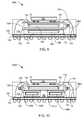
- FIG. 5therein is shown a cross-sectional view of an integrated circuit package system 500 in a third alternative embodiment of the present invention.
- the cross-sectional view of the integrated circuit package system 500depicts the first integrated circuit 114 mounted over the integrated circuit substrate 102 .
- An internal stacking module 502may include the flexible substrate 126 having the first side 128 and the second side 130 .
- the internal stacking module 502may be coupled to the active side of the first integrated circuit 114 by the chip interconnects 122 .
- the underfill material 124may be applied between the second side 130 of the flexible substrate 126 , the mold cap 138 , and the active side of the first integrated circuit 114 .
- the internal stacking module 502may be formed by the flexible substrate 126 having the first side 128 and the second side 130 .
- the first side 128 and the second side 130may provide an electrical connection path between the stacking module integrated circuit 132 , the discrete component 134 , the first integrated circuit 114 , the external integrated circuit 136 , or the combination thereof.
- the stacking module integrated circuit 132may be mounted, on the first side 128 of the flexible substrate 126 , by the adhesive 116 .
- the electrical interconnect 118may couple the active side of the stacking module integrated circuit 132 to the first side 128 of the flexible substrate 126 .
- the internal stacking module 502may be similar to the internal stacking module 120 , of FIG. 1 , but the position is inverted.
- the mold cap 138may be formed on the stacking module integrated circuit 132 , the electrical interconnect 118 , and the first side 128 of the flexible substrate 126 .
- the adhesive 116may be applied on the mold cap 138 , over the stacking module integrated circuit 132 , for sticking the first side 128 to the mold cap 138 .
- the discrete component 134may be electrically connected to the second side 130 of the flexible substrate 126 .
- the package body 140may be formed on the component side 104 , the first integrated circuit 114 , the electrical interconnect 118 , and the internal stacking module 502 .
- the package body 140does not cover the external component contacts 142 on the second side 130 of the flexible substrate 126 .
- the external integrated circuit 136may be electrically connected to the external component contacts 142 by the chip interconnects 122 .
- FIG. 6therein is shown a cross-sectional view of an integrated circuit package system 600 in a fourth alternative embodiment of the present invention.
- the cross-sectional view of the integrated circuit package system 600depicts the first integrated circuit 114 mounted over the integrated circuit substrate 102 .
- An internal stacking module 602may include the flexible substrate 126 having the first side 128 and the second side 130 .
- the internal stacking module 602may be coupled to the active side of the first integrated circuit 114 by the chip interconnects 122 .
- the underfill material 124may optionally be applied between the second side 130 of the flexible substrate 126 and the active side of the first integrated circuit 114 .
- the internal stacking module 602may be formed by the flexible substrate 126 having the first side 128 and the second side 130 .
- the first side 128 and the second side 130may provide an electrical connection path between the stacking module integrated circuit 132 , the discrete component 134 , the first integrated circuit 114 , the external integrated circuit 136 , or the combination thereof.
- the stacking module integrated circuit 132may be mounted, on the first side 128 of the flexible substrate 126 , by the adhesive 116 .
- the electrical interconnect 118may couple the active side of the stacking module integrated circuit 132 to the first side 128 of the flexible substrate 126 .
- the mold cap 138may be formed on the stacking module integrated circuit 132 , the electrical interconnect 118 , and the first side 128 of the flexible substrate 126 .
- the adhesive 116may be applied on the mold cap 138 , over the stacking module integrated circuit 132 , for sticking the first side 128 to the top of the mold cap 138 .
- the discrete component 134may be electrically connected to the second side 130 of the flexible substrate 126 .
- the package body 140may be formed on the component side 104 , the first integrated circuit 114 , the electrical interconnect 118 , and the internal stacking module 602 .
- the package body 140does not cover the external component contacts 142 on the second side 130 of the flexible substrate 126 .
- the external integrated circuit 136may be electrically connected to the external component contacts 142 by the chip interconnects 122 .
- FIG. 7therein is shown a cross-sectional view of an integrated circuit package system 700 in a fifth alternative embodiment of the present invention.
- the cross-sectional view of the integrated circuit package system 700depicts an internal stacking module 702 which may include the flexible substrate 126 having the first side 128 and the second side 130 .
- the internal stacking module 702may be coupled to the integrated circuit substrate 102 by the chip interconnects 122 .
- the underfill material 124may optionally be applied between the second side 130 of the flexible substrate 126 and the integrated circuit substrate 102 .
- the internal stacking module 702may be formed by the flexible substrate 126 having the first side 128 and the second side 130 .
- the first side 128 and the second side 130may provide an electrical connection path between the stacking module integrated circuit 132 , the discrete component 134 , a second stacking module integrated circuit 704 , the external integrated circuit 136 , or the combination thereof.
- the stacking module integrated circuit 132 and the second stacking module integrated circuit 704may be mounted, on the first side 128 of the flexible substrate 126 , by the adhesive 116 .
- the electrical interconnect 118may couple the active side of the stacking module integrated circuit 132 and the active side of the second stacking module integrated circuit 704 to the first side 128 of the flexible substrate 126 .
- the mold cap 138may be formed on the stacking module integrated circuit 132 , the electrical interconnect 118 , and the first side 128 of the flexible substrate 126 .
- a second mold cap 706may be formed on the second stacking module integrated circuit 704 , the electrical interconnect 118 , and the first side 128 of the flexible substrate 126 .
- the adhesive 116may be applied on the mold cap 138 , over the stacking module integrated circuit 132 , for sticking the top of the second mold cap 706 to the top of the mold cap 138 .
- This embodiment of the present inventionmay provide a vertical stack, of the stacking module integrated circuit 132 and the second stacking module integrated circuit 704 , within the internal stacking module 702 .
- the discrete component 134may be electrically connected to the second side 130 of the flexible substrate 126 .
- the package body 140may be formed on the component side 104 , the underfill material 124 , and the internal stacking module 702 . If the underfill material 124 is not present, the package body 140 will also be on the chip interconnects 122 .
- the package body 140does not cover the external component contacts 142 on the second side 130 of the flexible substrate 126 .
- the external integrated circuit 136may be electrically connected to the external component contacts 142 by the chip interconnects 122 .
- FIG. 8therein is shown a cross-sectional view of an integrated circuit package system 800 in a sixth alternative embodiment of the present invention.
- the cross-sectional view of the integrated circuit package system 800depicts an internal stacking module 802 which may include the flexible substrate 126 having the first side 128 and the second side 130 .
- the internal stacking module 802may be coupled to the integrated circuit substrate 102 by the chip interconnects 122 .
- the underfill material 124may optionally be applied between the second side 130 of the flexible substrate 126 and the integrated circuit substrate 102 .
- the internal stacking module 802may be formed by the flexible substrate 126 having the first side 128 and the second side 130 .
- the first side 128 and the second side 130may provide an electrical connection path between the stacking module integrated circuit 132 , the discrete component 134 , a second stacking module integrated circuit 804 , the external integrated circuit 136 , or the combination thereof.
- the stacking module integrated circuit 132 and the second stacking module integrated circuit 804may be mounted, on the first side 128 of the flexible substrate 126 , by the adhesive 116 .
- the electrical interconnect 118may couple the active side of the stacking module integrated circuit 132 and the active side of the second stacking module integrated circuit 804 to the first side 128 of the flexible substrate 126 .
- the mold cap 138may be formed on the stacking module integrated circuit 132 , the electrical interconnect 118 , and the first side 128 of the flexible substrate 126 .
- a second mold cap 806may be formed on the second stacking module integrated circuit 804 , the electrical interconnect 118 , and the first side 128 of the flexible substrate 126 .
- the adhesive 116may be applied on the mold cap 138 , over the stacking module integrated circuit 132 , for sticking the first side 128 to the top of the mold cap 138 .
- the adhesive 116may be applied on the second mold cap 806 , over the second stacking module integrated circuit 804 , for sticking the first side 128 to the top of the second mold cap 806 .
- This embodiment of the present inventionmay provide a horizontal mounting, of the stacking module integrated circuit 132 and the second stacking module integrated circuit 804 , within the internal stacking module 802 .
- An additional positionmay be provided for the discrete component 134 by positioning it in the opening of the flexible substrate 126 between the mold cap 138 and the second mold cap 806 . If the underfill material 124 is not used in this embodiment, the space would be filled by the package body 140 .
- the discrete component 134may be electrically connected to the second side 130 of the flexible substrate 126 .
- the package body 140may be formed on the component side 104 , the underfill material 124 , and the internal stacking module 802 .
- the package body 140does not cover the external component contacts 142 on the second side 130 of the flexible substrate 126 .
- the external integrated circuit 136may be electrically connected to the external component contacts 142 by the chip interconnects 122 .
- FIG. 9therein is shown a cross-sectional view of an integrated circuit package system 900 in a seventh alternative embodiment of the present invention.
- the cross-sectional view of the integrated circuit package system 900depicts an internal stacking module 902 which may include the flexible substrate 126 having the first side 128 and the second side 130 .
- the internal stacking module 902may be coupled to the integrated circuit substrate 102 by the electrical interconnects 118 .
- the internal stacking module 902may be formed by the flexible substrate 126 having the first side 128 and the second side 130 .
- the first side 128 and the second side 130may provide an electrical connection path between the stacking module integrated circuit 132 , the discrete component 134 , a second stacking module integrated circuit 904 , the external integrated circuit 136 , or the combination thereof.
- the stacking module integrated circuit 132may be mounted on the first side 128 of the flexible substrate 126 by the adhesive 116 .
- the second stacking module integrated circuit 904may be mounted on the second side 130 of the flexible substrate 126 by the adhesive 116 .
- the electrical interconnect 118may couple the active side of the stacking module integrated circuit 132 to the first side 128 of the flexible substrate 126 and the active side of the second stacking module integrated circuit 904 to the second side 130 .
- the mold cap 138may be formed on the stacking module integrated circuit 132 , the electrical interconnect 118 , and the first side 128 of the flexible substrate 126 .
- a second mold cap 906may be formed on the second stacking module integrated circuit 904 , the electrical interconnect 118 , and the second side 130 of the flexible substrate 126 .
- the adhesive 116may be applied on the mold cap 138 , over the stacking module integrated circuit 132 , for sticking the first side 128 to the top of the mold cap 138 .
- the adhesive 116may be applied on the second mold cap 906 , over the second stacking module integrated circuit 804 , for sticking the top of the second mold cap 906 to the component side 104 of the integrated circuit substrate 102 .
- This embodiment of the present inventionmay provide a vertical mounting, of the stacking module integrated circuit 132 and the second stacking module integrated circuit 904 , within the internal stacking module 902 .
- the discrete component 134may be electrically connected to the second side 130 of the flexible substrate 126 .
- the package body 140may be formed on the component side 104 , the electrical interconnects 118 , and the internal stacking module 902 .
- the package body 140does not cover the external component contacts 142 on the second side 130 of the flexible substrate 126 .
- the external integrated circuit 136may be electrically connected to the external component contacts 142 by the chip interconnects 122 .
- FIG. 10therein is shown a cross-sectional view of an integrated circuit package system 1000 in an eighth alternative embodiment of the present invention.
- the cross-sectional view of the integrated circuit package system 1000depicts an internal stacking module 1002 which may include the flexible substrate 126 having the first side 128 and the second side 130 .
- the internal stacking module 1002may be coupled to the integrated circuit substrate 102 by the electrical interconnects 118 .
- the internal stacking module 1002may be formed by the flexible substrate 126 having the first side 128 and the second side 130 .
- the first side 128 and the second side 130may provide an electrical connection path between the stacking module integrated circuit 132 , the discrete component 134 , a second stacking module integrated circuit 1004 , a third stacking module integrated circuit 1006 , the external integrated circuit 136 , or the combination thereof.
- the stacking module integrated circuit 132may be mounted on the first side 128 of the flexible substrate 126 by the adhesive 116 . While the second stacking module integrated circuit 1004 and the third stacking module integrated circuit 1006 may be mounted on the second side 130 of the flexible substrate 126 by the adhesive 116 .
- the electrical interconnect 118may couple the active side of the stacking module integrated circuit 132 to the first side 128 of the flexible substrate 126 and the active side of the second stacking module integrated circuit 1004 and the third stacking module integrated circuit 1006 to the second side 130 .
- the mold cap 138may be formed on the stacking module integrated circuit 132 , the electrical interconnect 118 , and the first side 128 of the flexible substrate 126 .
- a second mold cap 1008may be formed on the second stacking module integrated circuit 1004 , the electrical interconnect 118 , and the second side 130 of the flexible substrate 126 .
- a third mold cap 1010may be formed on the third stacking module integrated circuit 1006 , the electrical interconnect 118 , and the second side 130 of the flexible substrate 126 .
- the adhesive 116may be applied on the mold cap 138 for sticking the first side 128 to the top of the mold cap 138 .
- the adhesive 116may be applied on the second mold cap 1008 for sticking the top of the second mold cap 1008 to the component side 104 of the integrated circuit substrate 102 .
- the adhesive 116may be applied on the third mold cap 1010 for sticking the top of the third mold cap 1010 to the component side 104 of the integrated circuit substrate 102 .
- This embodiment of the present inventionmay provide a vertical mounting, of the stacking module integrated circuit 132 over the second stacking module integrated circuit 1004 and the third stacking module integrated circuit 1006 within the internal stacking module 1002 .
- the discrete component 134may be electrically connected to the second side 130 of the flexible substrate 126 .
- An additional positionmay be provided for the discrete component 134 by positioning it in the opening of the flexible substrate 126 between the second mold cap 1008 and the third mold cap 1010 . In this embodiment, the space would be filled by the package body 140 .
- the package body 140may be formed on the component side 104 , the electrical interconnects 118 , and the internal stacking module 1002 .
- the package body 140does not cover the external component contacts 142 on the second side 130 of the flexible substrate 126 .
- the external integrated circuit 136may be electrically connected to the external component contacts 142 by the chip interconnects 122 .
- the system 1100includes fabricating an integrated circuit substrate in a block 1102 ; forming an internal stacking module coupled to the integrated circuit substrate including: forming a flexible substrate, coupling a stacking module integrated circuit to the flexible substrate, and bending a flexible extension over the stacking module integrated circuit in a block 1104 ; molding a package body on the integrated circuit substrate and the internal stacking module in a block 1106 ; and coupling an external integrated circuit to the internal stacking module exposed through the package body in a block 1108 .
- An aspect of the present inventionis that it valuably supports and services the historical trend of reducing costs, simplifying systems, and increasing performance.
- the integrated circuit package system with internal stacking module of the present inventionfurnishes important and heretofore unknown and unavailable solutions, capabilities, and functional aspects for fabricating integrated circuit packages having a built-in package stacking capability.
- the resulting processes and configurationsare straightforward, cost-effective, uncomplicated, highly versatile and effective, can be surprisingly and unobviously implemented by adapting known technologies, and are thus readily suited for efficiently and economically manufacturing multi-function integrated circuit devices, such as system-in-package (SIP), fully compatible with conventional manufacturing processes and technologies.
- SIPsystem-in-package
- the resulting processes and configurationsare straightforward, cost-effective, uncomplicated, highly versatile, accurate, sensitive, and effective, and can be implemented by adapting known components for ready, efficient, and economical manufacturing, application, and utilization.
Landscapes
- Engineering & Computer Science (AREA)
- Microelectronics & Electronic Packaging (AREA)
- Power Engineering (AREA)
- Physics & Mathematics (AREA)
- Condensed Matter Physics & Semiconductors (AREA)
- General Physics & Mathematics (AREA)
- Computer Hardware Design (AREA)
- Health & Medical Sciences (AREA)
- Electromagnetism (AREA)
- Toxicology (AREA)
- Manufacturing & Machinery (AREA)
- Structures Or Materials For Encapsulating Or Coating Semiconductor Devices Or Solid State Devices (AREA)
Abstract
Description
Claims (19)
Priority Applications (2)
| Application Number | Priority Date | Filing Date | Title |
|---|---|---|---|
| US12/137,529US8278141B2 (en) | 2008-06-11 | 2008-06-11 | Integrated circuit package system with internal stacking module |
| US13/563,598US9030006B2 (en) | 2008-06-09 | 2012-07-31 | Integrated circuit package system with internal stacking module |
Applications Claiming Priority (1)
| Application Number | Priority Date | Filing Date | Title |
|---|---|---|---|
| US12/137,529US8278141B2 (en) | 2008-06-11 | 2008-06-11 | Integrated circuit package system with internal stacking module |
Related Child Applications (1)
| Application Number | Title | Priority Date | Filing Date |
|---|---|---|---|
| US13/563,598ContinuationUS9030006B2 (en) | 2008-06-09 | 2012-07-31 | Integrated circuit package system with internal stacking module |
Publications (2)
| Publication Number | Publication Date |
|---|---|
| US20090309197A1 US20090309197A1 (en) | 2009-12-17 |
| US8278141B2true US8278141B2 (en) | 2012-10-02 |
Family
ID=41413967
Family Applications (2)
| Application Number | Title | Priority Date | Filing Date |
|---|---|---|---|
| US12/137,529Active2029-04-03US8278141B2 (en) | 2008-06-09 | 2008-06-11 | Integrated circuit package system with internal stacking module |
| US13/563,598ActiveUS9030006B2 (en) | 2008-06-09 | 2012-07-31 | Integrated circuit package system with internal stacking module |
Family Applications After (1)
| Application Number | Title | Priority Date | Filing Date |
|---|---|---|---|
| US13/563,598ActiveUS9030006B2 (en) | 2008-06-09 | 2012-07-31 | Integrated circuit package system with internal stacking module |
Country Status (1)
| Country | Link |
|---|---|
| US (2) | US8278141B2 (en) |
Cited By (43)
| Publication number | Priority date | Publication date | Assignee | Title |
|---|---|---|---|---|
| US20060138649A1 (en)* | 2002-10-08 | 2006-06-29 | Chippac, Inc. | Semiconductor multi-package module having inverted second package stacked over die-up flip-chip ball grid array (BGA) package |
| US20120061846A1 (en)* | 2009-06-02 | 2012-03-15 | Hsio Technologies, Llc | Compliant printed circuit area array semiconductor device package |
| US20140192488A1 (en)* | 2009-09-08 | 2014-07-10 | Apple Inc. | Handheld device assembly |
| US8789272B2 (en) | 2009-06-02 | 2014-07-29 | Hsio Technologies, Llc | Method of making a compliant printed circuit peripheral lead semiconductor test socket |
| US8803539B2 (en) | 2009-06-03 | 2014-08-12 | Hsio Technologies, Llc | Compliant wafer level probe assembly |
| US8912812B2 (en) | 2009-06-02 | 2014-12-16 | Hsio Technologies, Llc | Compliant printed circuit wafer probe diagnostic tool |
| US8928344B2 (en) | 2009-06-02 | 2015-01-06 | Hsio Technologies, Llc | Compliant printed circuit socket diagnostic tool |
| US8955215B2 (en) | 2009-05-28 | 2015-02-17 | Hsio Technologies, Llc | High performance surface mount electrical interconnect |
| US8955216B2 (en) | 2009-06-02 | 2015-02-17 | Hsio Technologies, Llc | Method of making a compliant printed circuit peripheral lead semiconductor package |
| US8970031B2 (en) | 2009-06-16 | 2015-03-03 | Hsio Technologies, Llc | Semiconductor die terminal |
| US8981809B2 (en) | 2009-06-29 | 2015-03-17 | Hsio Technologies, Llc | Compliant printed circuit semiconductor tester interface |
| US8981568B2 (en) | 2009-06-16 | 2015-03-17 | Hsio Technologies, Llc | Simulated wirebond semiconductor package |
| US8984748B2 (en) | 2009-06-29 | 2015-03-24 | Hsio Technologies, Llc | Singulated semiconductor device separable electrical interconnect |
| US8988093B2 (en) | 2009-06-02 | 2015-03-24 | Hsio Technologies, Llc | Bumped semiconductor wafer or die level electrical interconnect |
| US8987886B2 (en) | 2009-06-02 | 2015-03-24 | Hsio Technologies, Llc | Copper pillar full metal via electrical circuit structure |
| US9076884B2 (en) | 2009-06-02 | 2015-07-07 | Hsio Technologies, Llc | Compliant printed circuit semiconductor package |
| US9093767B2 (en) | 2009-06-02 | 2015-07-28 | Hsio Technologies, Llc | High performance surface mount electrical interconnect |
| US9136196B2 (en) | 2009-06-02 | 2015-09-15 | Hsio Technologies, Llc | Compliant printed circuit wafer level semiconductor package |
| US9184527B2 (en) | 2009-06-02 | 2015-11-10 | Hsio Technologies, Llc | Electrical connector insulator housing |
| US9184145B2 (en) | 2009-06-02 | 2015-11-10 | Hsio Technologies, Llc | Semiconductor device package adapter |
| US9232654B2 (en) | 2009-06-02 | 2016-01-05 | Hsio Technologies, Llc | High performance electrical circuit structure |
| US9231328B2 (en) | 2009-06-02 | 2016-01-05 | Hsio Technologies, Llc | Resilient conductive electrical interconnect |
| US9276336B2 (en) | 2009-05-28 | 2016-03-01 | Hsio Technologies, Llc | Metalized pad to electrical contact interface |
| US9276339B2 (en) | 2009-06-02 | 2016-03-01 | Hsio Technologies, Llc | Electrical interconnect IC device socket |
| US9277654B2 (en) | 2009-06-02 | 2016-03-01 | Hsio Technologies, Llc | Composite polymer-metal electrical contacts |
| US9320133B2 (en) | 2009-06-02 | 2016-04-19 | Hsio Technologies, Llc | Electrical interconnect IC device socket |
| US9320144B2 (en) | 2009-06-17 | 2016-04-19 | Hsio Technologies, Llc | Method of forming a semiconductor socket |
| US9318862B2 (en) | 2009-06-02 | 2016-04-19 | Hsio Technologies, Llc | Method of making an electronic interconnect |
| US9350093B2 (en) | 2010-06-03 | 2016-05-24 | Hsio Technologies, Llc | Selective metalization of electrical connector or socket housing |
| US9414500B2 (en) | 2009-06-02 | 2016-08-09 | Hsio Technologies, Llc | Compliant printed flexible circuit |
| US9536815B2 (en) | 2009-05-28 | 2017-01-03 | Hsio Technologies, Llc | Semiconductor socket with direct selective metalization |
| US9559447B2 (en) | 2015-03-18 | 2017-01-31 | Hsio Technologies, Llc | Mechanical contact retention within an electrical connector |
| US9613841B2 (en) | 2009-06-02 | 2017-04-04 | Hsio Technologies, Llc | Area array semiconductor device package interconnect structure with optional package-to-package or flexible circuit to package connection |
| US9689897B2 (en) | 2010-06-03 | 2017-06-27 | Hsio Technologies, Llc | Performance enhanced semiconductor socket |
| US9699906B2 (en) | 2009-06-02 | 2017-07-04 | Hsio Technologies, Llc | Hybrid printed circuit assembly with low density main core and embedded high density circuit regions |
| US9761520B2 (en) | 2012-07-10 | 2017-09-12 | Hsio Technologies, Llc | Method of making an electrical connector having electrodeposited terminals |
| US9871012B2 (en) | 2012-08-31 | 2018-01-16 | Qualcomm Incorporated | Method and apparatus for routing die signals using external interconnects |
| US9930775B2 (en) | 2009-06-02 | 2018-03-27 | Hsio Technologies, Llc | Copper pillar full metal via electrical circuit structure |
| US20180106774A1 (en)* | 2016-10-19 | 2018-04-19 | Winbond Electronics Corp. | Sensor array, manufacturing method thereof, and sensing method |
| US10159154B2 (en) | 2010-06-03 | 2018-12-18 | Hsio Technologies, Llc | Fusion bonded liquid crystal polymer circuit structure |
| US20190067245A1 (en)* | 2017-08-22 | 2019-02-28 | Micron Technology, Inc. | Integrated semiconductor assemblies and methods of manufacturing the same |
| US10506722B2 (en) | 2013-07-11 | 2019-12-10 | Hsio Technologies, Llc | Fusion bonded liquid crystal polymer electrical circuit structure |
| US10667410B2 (en) | 2013-07-11 | 2020-05-26 | Hsio Technologies, Llc | Method of making a fusion bonded circuit structure |
Families Citing this family (21)
| Publication number | Priority date | Publication date | Assignee | Title |
|---|---|---|---|---|
| US8072058B2 (en)* | 2004-10-25 | 2011-12-06 | Amkor Technology, Inc. | Semiconductor package having a plurality input/output members |
| KR101078743B1 (en) | 2010-04-14 | 2011-11-02 | 주식회사 하이닉스반도체 | stack package |
| JP5614203B2 (en)* | 2010-09-24 | 2014-10-29 | 日本電気株式会社 | Semiconductor device and manufacturing method thereof |
| US9768102B2 (en)* | 2012-03-21 | 2017-09-19 | STATS ChipPAC Pte. Ltd. | Integrated circuit packaging system with support structure and method of manufacture thereof |
| FR3011978A1 (en)* | 2013-10-15 | 2015-04-17 | St Microelectronics Grenoble 2 | ELECTRONIC SYSTEM COMPRISING STACKED ELECTRONIC DEVICES COMPRISING INTEGRATED CIRCUIT CHIPS |
| JP6467640B2 (en)* | 2014-01-16 | 2019-02-13 | パナソニックIpマネジメント株式会社 | Semiconductor device |
| KR20160066311A (en)* | 2014-12-02 | 2016-06-10 | 삼성전기주식회사 | semi-conductor package and manufacturing method thereof |
| FR3038130B1 (en)* | 2015-06-25 | 2017-08-11 | 3D Plus | 3D ELECTRONIC MODULE COMPRISING A STACK OF BALL CASES |
| CN105118820B (en)* | 2015-07-21 | 2017-12-19 | 三星半导体(中国)研究开发有限公司 | Packaging part and its manufacture method, encapsulation stacking structure and its manufacture method |
| DE102015219190A1 (en)* | 2015-10-05 | 2017-04-06 | Fraunhofer-Gesellschaft zur Förderung der angewandten Forschung e.V. | Method for producing an electronic component and electronic component |
| US9842828B1 (en)* | 2016-06-13 | 2017-12-12 | Stmicroelectronics, Inc. | Stacked semiconductor package with compliant corners on folded substrate |
| JP7015691B2 (en)* | 2017-12-27 | 2022-02-03 | 新光電気工業株式会社 | Semiconductor device |
| US11145621B2 (en)* | 2018-06-06 | 2021-10-12 | Advanced Semiconductor Engineering, Inc. | Semiconductor package device and method of manufacturing the same |
| KR20200067607A (en)* | 2018-12-04 | 2020-06-12 | 삼성전기주식회사 | Printed circuit board |
| TWI692065B (en)* | 2019-09-04 | 2020-04-21 | 力成科技股份有限公司 | System package with high component density |
| US11652064B2 (en)* | 2019-12-06 | 2023-05-16 | Qualcomm Incorporated | Integrated device with electromagnetic shield |
| CN111739873B (en)* | 2020-08-11 | 2020-11-20 | 甬矽电子(宁波)股份有限公司 | Flexible substrate lamination packaging structure and flexible substrate lamination packaging method |
| TWI762058B (en)* | 2020-12-02 | 2022-04-21 | 恆勁科技股份有限公司 | Semiconductor package device |
| CN113823626B (en)* | 2021-09-23 | 2023-10-31 | 华东光电集成器件研究所 | Acceleration value recording device for penetration measurement based on fan-out technology |
| CN114156251B (en)* | 2021-11-03 | 2025-08-22 | 青岛歌尔智能传感器有限公司 | SIP packaging structure and electronic device |
| US20240105687A1 (en)* | 2022-09-23 | 2024-03-28 | Qualcomm Incorporated | Package comprising a flexible substrate |
Citations (36)
| Publication number | Priority date | Publication date | Assignee | Title |
|---|---|---|---|---|
| US5646446A (en)* | 1995-12-22 | 1997-07-08 | Fairchild Space And Defense Corporation | Three-dimensional flexible assembly of integrated circuits |
| US6683377B1 (en) | 2000-05-30 | 2004-01-27 | Amkor Technology, Inc. | Multi-stacked memory package |
| US6765288B2 (en) | 2002-08-05 | 2004-07-20 | Tessera, Inc. | Microelectronic adaptors, assemblies and methods |
| US20040209400A1 (en)* | 2002-08-26 | 2004-10-21 | Meyers John G. | Process and apparatus for packaging a tape substrate |
| US6841855B2 (en) | 2003-04-28 | 2005-01-11 | Intel Corporation | Electronic package having a flexible substrate with ends connected to one another |
| US6869825B2 (en) | 2002-12-31 | 2005-03-22 | Intel Corporation | Folded BGA package design with shortened communication paths and more electrical routing flexibility |
| US6884653B2 (en) | 2001-03-21 | 2005-04-26 | Micron Technology, Inc. | Folded interposer |
| US6924551B2 (en) | 2003-05-28 | 2005-08-02 | Intel Corporation | Through silicon via, folded flex microelectronic package |
| US6933598B2 (en) | 2002-10-08 | 2005-08-23 | Chippac, Inc. | Semiconductor stacked multi-package module having inverted second package and electrically shielded first package |
| US6940729B2 (en) | 2001-10-26 | 2005-09-06 | Staktek Group L.P. | Integrated circuit stacking system and method |
| US20050199971A1 (en)* | 2002-03-06 | 2005-09-15 | Anderson Richard S. | Integrated sensor and electronics package |
| US20060033217A1 (en) | 2004-08-10 | 2006-02-16 | Brian Taggart | Flip-chips on flex substrates, flip-chip and wire-bonded chip stacks, and methods of assembling same |
| US20060077644A1 (en)* | 2004-10-13 | 2006-04-13 | Nickerson Robert M | Folded substrate with interposer package for integrated circuit devices |
| US7033911B2 (en) | 2004-03-31 | 2006-04-25 | Intel Corporation | Adhesive of folded package |
| US7053478B2 (en) | 2001-10-26 | 2006-05-30 | Staktek Group L.P. | Pitch change and chip scale stacking system |
| US20060138630A1 (en) | 2004-12-28 | 2006-06-29 | Netlist, Inc. | Stacked ball grid array packages |
| US7115986B2 (en) | 2001-05-02 | 2006-10-03 | Micron Technology, Inc. | Flexible ball grid array chip scale packages |
| US20060226543A1 (en)* | 2003-03-05 | 2006-10-12 | Samsung Electronics Co., Ltd. | Ball grid array package stack |
| US7149095B2 (en) | 1996-12-13 | 2006-12-12 | Tessera, Inc. | Stacked microelectronic assemblies |
| US7154171B1 (en) | 2002-02-22 | 2006-12-26 | Amkor Technology, Inc. | Stacking structure for semiconductor devices using a folded over flexible substrate and method therefor |
| US7154175B2 (en) | 2004-06-21 | 2006-12-26 | Intel Corporation | Ground plane for integrated circuit package |
| US7183140B2 (en) | 2004-11-08 | 2007-02-27 | Intel Corporation | Injection molded metal bonding tray for integrated circuit device fabrication |
| US7205647B2 (en) | 2002-09-17 | 2007-04-17 | Chippac, Inc. | Semiconductor multi-package module having package stacked over ball grid array package and having wire bond interconnect between stacked packages |
| US20070114649A1 (en)* | 2001-10-26 | 2007-05-24 | Staktek Group L.P., A Texas Limited Partnership | Low Profile Stacking System and Method |
| US7230328B2 (en) | 2002-11-20 | 2007-06-12 | Nec Corporation | Semiconductor package and laminated semiconductor package |
| US7235870B2 (en) | 2004-12-30 | 2007-06-26 | Punzalan Jr Nelson V | Microelectronic multi-chip module |
| US20070187826A1 (en)* | 2006-02-14 | 2007-08-16 | Stats Chippac Ltd. | 3-d package stacking system |
| US20070194423A1 (en)* | 2006-02-17 | 2007-08-23 | Stats Chippac Ltd. | Stacked integrated circuit package-in-package system with recessed spacer |
| US20070194463A1 (en)* | 2006-02-21 | 2007-08-23 | Young Cheol Kim | Integrated circuit package system with l-shaped leadfingers |
| US20080009096A1 (en)* | 2006-07-10 | 2008-01-10 | Samsung Electronics Co., Ltd. | Package-on-package and method of fabricating the same |
| US20080029905A1 (en)* | 2006-08-04 | 2008-02-07 | Stats Chippac Ltd. | Integrated circuit package-in-package system |
| US20090016033A1 (en) | 2007-07-12 | 2009-01-15 | Seng Guan Chow | Integrated circuit package system with flexible substrate and mounded package |
| US20090016032A1 (en) | 2007-07-12 | 2009-01-15 | Seng Guan Chow | Integrated circuit package system with flexible substrate and recessed package |
| US20090115032A1 (en)* | 2007-11-07 | 2009-05-07 | Zigmund Ramirez Camacho | Integrated circuit package system with dual connectivity |
| US20090206461A1 (en)* | 2008-02-15 | 2009-08-20 | Qimonda Ag | Integrated circuit and method |
| US20090236753A1 (en)* | 2008-03-21 | 2009-09-24 | Moon Dongsoo | Integrated circuit package system for stackable devices |
Family Cites Families (4)
| Publication number | Priority date | Publication date | Assignee | Title |
|---|---|---|---|---|
| US7986043B2 (en)* | 2006-03-08 | 2011-07-26 | Stats Chippac Ltd. | Integrated circuit package on package system |
| US7288835B2 (en) | 2006-03-17 | 2007-10-30 | Stats Chippac Ltd. | Integrated circuit package-in-package system |
| US20090243069A1 (en)* | 2008-03-26 | 2009-10-01 | Zigmund Ramirez Camacho | Integrated circuit package system with redistribution |
| US8072047B2 (en)* | 2008-05-21 | 2011-12-06 | Stats Chippac Ltd. | Integrated circuit package system with shield and tie bar |
- 2008
- 2008-06-11USUS12/137,529patent/US8278141B2/enactiveActive
- 2012
- 2012-07-31USUS13/563,598patent/US9030006B2/enactiveActive
Patent Citations (38)
| Publication number | Priority date | Publication date | Assignee | Title |
|---|---|---|---|---|
| US5646446A (en)* | 1995-12-22 | 1997-07-08 | Fairchild Space And Defense Corporation | Three-dimensional flexible assembly of integrated circuits |
| US7149095B2 (en) | 1996-12-13 | 2006-12-12 | Tessera, Inc. | Stacked microelectronic assemblies |
| US6683377B1 (en) | 2000-05-30 | 2004-01-27 | Amkor Technology, Inc. | Multi-stacked memory package |
| US6884653B2 (en) | 2001-03-21 | 2005-04-26 | Micron Technology, Inc. | Folded interposer |
| US6982869B2 (en) | 2001-03-21 | 2006-01-03 | Micron Technology, Inc. | Folded interposer |
| US7115986B2 (en) | 2001-05-02 | 2006-10-03 | Micron Technology, Inc. | Flexible ball grid array chip scale packages |
| US6940729B2 (en) | 2001-10-26 | 2005-09-06 | Staktek Group L.P. | Integrated circuit stacking system and method |
| US20070114649A1 (en)* | 2001-10-26 | 2007-05-24 | Staktek Group L.P., A Texas Limited Partnership | Low Profile Stacking System and Method |
| US7053478B2 (en) | 2001-10-26 | 2006-05-30 | Staktek Group L.P. | Pitch change and chip scale stacking system |
| US7154171B1 (en) | 2002-02-22 | 2006-12-26 | Amkor Technology, Inc. | Stacking structure for semiconductor devices using a folded over flexible substrate and method therefor |
| US20050199971A1 (en)* | 2002-03-06 | 2005-09-15 | Anderson Richard S. | Integrated sensor and electronics package |
| US6765288B2 (en) | 2002-08-05 | 2004-07-20 | Tessera, Inc. | Microelectronic adaptors, assemblies and methods |
| US20040209400A1 (en)* | 2002-08-26 | 2004-10-21 | Meyers John G. | Process and apparatus for packaging a tape substrate |
| US7205647B2 (en) | 2002-09-17 | 2007-04-17 | Chippac, Inc. | Semiconductor multi-package module having package stacked over ball grid array package and having wire bond interconnect between stacked packages |
| US6933598B2 (en) | 2002-10-08 | 2005-08-23 | Chippac, Inc. | Semiconductor stacked multi-package module having inverted second package and electrically shielded first package |
| US7230328B2 (en) | 2002-11-20 | 2007-06-12 | Nec Corporation | Semiconductor package and laminated semiconductor package |
| US6869825B2 (en) | 2002-12-31 | 2005-03-22 | Intel Corporation | Folded BGA package design with shortened communication paths and more electrical routing flexibility |
| US20060226543A1 (en)* | 2003-03-05 | 2006-10-12 | Samsung Electronics Co., Ltd. | Ball grid array package stack |
| US6841855B2 (en) | 2003-04-28 | 2005-01-11 | Intel Corporation | Electronic package having a flexible substrate with ends connected to one another |
| US6924551B2 (en) | 2003-05-28 | 2005-08-02 | Intel Corporation | Through silicon via, folded flex microelectronic package |
| US7033911B2 (en) | 2004-03-31 | 2006-04-25 | Intel Corporation | Adhesive of folded package |
| US7154175B2 (en) | 2004-06-21 | 2006-12-26 | Intel Corporation | Ground plane for integrated circuit package |
| US20060033217A1 (en) | 2004-08-10 | 2006-02-16 | Brian Taggart | Flip-chips on flex substrates, flip-chip and wire-bonded chip stacks, and methods of assembling same |
| US7358444B2 (en) | 2004-10-13 | 2008-04-15 | Intel Corporation | Folded substrate with interposer package for integrated circuit devices |
| US20060077644A1 (en)* | 2004-10-13 | 2006-04-13 | Nickerson Robert M | Folded substrate with interposer package for integrated circuit devices |
| US7183140B2 (en) | 2004-11-08 | 2007-02-27 | Intel Corporation | Injection molded metal bonding tray for integrated circuit device fabrication |
| US20060138630A1 (en) | 2004-12-28 | 2006-06-29 | Netlist, Inc. | Stacked ball grid array packages |
| US7235870B2 (en) | 2004-12-30 | 2007-06-26 | Punzalan Jr Nelson V | Microelectronic multi-chip module |
| US20070187826A1 (en)* | 2006-02-14 | 2007-08-16 | Stats Chippac Ltd. | 3-d package stacking system |
| US20070194423A1 (en)* | 2006-02-17 | 2007-08-23 | Stats Chippac Ltd. | Stacked integrated circuit package-in-package system with recessed spacer |
| US20070194463A1 (en)* | 2006-02-21 | 2007-08-23 | Young Cheol Kim | Integrated circuit package system with l-shaped leadfingers |
| US20080009096A1 (en)* | 2006-07-10 | 2008-01-10 | Samsung Electronics Co., Ltd. | Package-on-package and method of fabricating the same |
| US20080029905A1 (en)* | 2006-08-04 | 2008-02-07 | Stats Chippac Ltd. | Integrated circuit package-in-package system |
| US20090016033A1 (en) | 2007-07-12 | 2009-01-15 | Seng Guan Chow | Integrated circuit package system with flexible substrate and mounded package |
| US20090016032A1 (en) | 2007-07-12 | 2009-01-15 | Seng Guan Chow | Integrated circuit package system with flexible substrate and recessed package |
| US20090115032A1 (en)* | 2007-11-07 | 2009-05-07 | Zigmund Ramirez Camacho | Integrated circuit package system with dual connectivity |
| US20090206461A1 (en)* | 2008-02-15 | 2009-08-20 | Qimonda Ag | Integrated circuit and method |
| US20090236753A1 (en)* | 2008-03-21 | 2009-09-24 | Moon Dongsoo | Integrated circuit package system for stackable devices |
Non-Patent Citations (2)
| Title |
|---|
| "McGraw Hill Dictionary of Scientific and Technical Terms. 5th Edition", ed. S. Parker, © 1994 McGraw Hill, Inc., p. 1027.* |
| "McGraw Hill, Dictionaly of Scientific and Technical Terms, 5th Edition", ed. S. Parker, © 1994 McGraw Hill.* |
Cited By (54)
| Publication number | Priority date | Publication date | Assignee | Title |
|---|---|---|---|---|
| US20060138649A1 (en)* | 2002-10-08 | 2006-06-29 | Chippac, Inc. | Semiconductor multi-package module having inverted second package stacked over die-up flip-chip ball grid array (BGA) package |
| US8955215B2 (en) | 2009-05-28 | 2015-02-17 | Hsio Technologies, Llc | High performance surface mount electrical interconnect |
| US9660368B2 (en) | 2009-05-28 | 2017-05-23 | Hsio Technologies, Llc | High performance surface mount electrical interconnect |
| US9536815B2 (en) | 2009-05-28 | 2017-01-03 | Hsio Technologies, Llc | Semiconductor socket with direct selective metalization |
| US9276336B2 (en) | 2009-05-28 | 2016-03-01 | Hsio Technologies, Llc | Metalized pad to electrical contact interface |
| US9699906B2 (en) | 2009-06-02 | 2017-07-04 | Hsio Technologies, Llc | Hybrid printed circuit assembly with low density main core and embedded high density circuit regions |
| US8789272B2 (en) | 2009-06-02 | 2014-07-29 | Hsio Technologies, Llc | Method of making a compliant printed circuit peripheral lead semiconductor test socket |
| US8928344B2 (en) | 2009-06-02 | 2015-01-06 | Hsio Technologies, Llc | Compliant printed circuit socket diagnostic tool |
| US20120061846A1 (en)* | 2009-06-02 | 2012-03-15 | Hsio Technologies, Llc | Compliant printed circuit area array semiconductor device package |
| US8955216B2 (en) | 2009-06-02 | 2015-02-17 | Hsio Technologies, Llc | Method of making a compliant printed circuit peripheral lead semiconductor package |
| US9613841B2 (en) | 2009-06-02 | 2017-04-04 | Hsio Technologies, Llc | Area array semiconductor device package interconnect structure with optional package-to-package or flexible circuit to package connection |
| US9414500B2 (en) | 2009-06-02 | 2016-08-09 | Hsio Technologies, Llc | Compliant printed flexible circuit |
| US9318862B2 (en) | 2009-06-02 | 2016-04-19 | Hsio Technologies, Llc | Method of making an electronic interconnect |
| US10609819B2 (en) | 2009-06-02 | 2020-03-31 | Hsio Technologies, Llc | Hybrid printed circuit assembly with low density main core and embedded high density circuit regions |
| US8988093B2 (en) | 2009-06-02 | 2015-03-24 | Hsio Technologies, Llc | Bumped semiconductor wafer or die level electrical interconnect |
| US8987886B2 (en) | 2009-06-02 | 2015-03-24 | Hsio Technologies, Llc | Copper pillar full metal via electrical circuit structure |
| US9054097B2 (en)* | 2009-06-02 | 2015-06-09 | Hsio Technologies, Llc | Compliant printed circuit area array semiconductor device package |
| US9076884B2 (en) | 2009-06-02 | 2015-07-07 | Hsio Technologies, Llc | Compliant printed circuit semiconductor package |
| US9093767B2 (en) | 2009-06-02 | 2015-07-28 | Hsio Technologies, Llc | High performance surface mount electrical interconnect |
| US9136196B2 (en) | 2009-06-02 | 2015-09-15 | Hsio Technologies, Llc | Compliant printed circuit wafer level semiconductor package |
| US9184527B2 (en) | 2009-06-02 | 2015-11-10 | Hsio Technologies, Llc | Electrical connector insulator housing |
| US9184145B2 (en) | 2009-06-02 | 2015-11-10 | Hsio Technologies, Llc | Semiconductor device package adapter |
| US9232654B2 (en) | 2009-06-02 | 2016-01-05 | Hsio Technologies, Llc | High performance electrical circuit structure |
| US9231328B2 (en) | 2009-06-02 | 2016-01-05 | Hsio Technologies, Llc | Resilient conductive electrical interconnect |
| US9930775B2 (en) | 2009-06-02 | 2018-03-27 | Hsio Technologies, Llc | Copper pillar full metal via electrical circuit structure |
| US9276339B2 (en) | 2009-06-02 | 2016-03-01 | Hsio Technologies, Llc | Electrical interconnect IC device socket |
| US9277654B2 (en) | 2009-06-02 | 2016-03-01 | Hsio Technologies, Llc | Composite polymer-metal electrical contacts |
| US9320133B2 (en) | 2009-06-02 | 2016-04-19 | Hsio Technologies, Llc | Electrical interconnect IC device socket |
| US8912812B2 (en) | 2009-06-02 | 2014-12-16 | Hsio Technologies, Llc | Compliant printed circuit wafer probe diagnostic tool |
| US8803539B2 (en) | 2009-06-03 | 2014-08-12 | Hsio Technologies, Llc | Compliant wafer level probe assembly |
| US8981568B2 (en) | 2009-06-16 | 2015-03-17 | Hsio Technologies, Llc | Simulated wirebond semiconductor package |
| US8970031B2 (en) | 2009-06-16 | 2015-03-03 | Hsio Technologies, Llc | Semiconductor die terminal |
| US9320144B2 (en) | 2009-06-17 | 2016-04-19 | Hsio Technologies, Llc | Method of forming a semiconductor socket |
| US8984748B2 (en) | 2009-06-29 | 2015-03-24 | Hsio Technologies, Llc | Singulated semiconductor device separable electrical interconnect |
| US8981809B2 (en) | 2009-06-29 | 2015-03-17 | Hsio Technologies, Llc | Compliant printed circuit semiconductor tester interface |
| US20140192489A1 (en)* | 2009-09-08 | 2014-07-10 | Apple Inc. | Handheld device assembly |
| US9386704B2 (en)* | 2009-09-08 | 2016-07-05 | Apple Inc. | Handheld device assembly |
| US20140192488A1 (en)* | 2009-09-08 | 2014-07-10 | Apple Inc. | Handheld device assembly |
| US9386705B2 (en)* | 2009-09-08 | 2016-07-05 | Apple Inc. | Handheld device assembly |
| US10159154B2 (en) | 2010-06-03 | 2018-12-18 | Hsio Technologies, Llc | Fusion bonded liquid crystal polymer circuit structure |
| US9689897B2 (en) | 2010-06-03 | 2017-06-27 | Hsio Technologies, Llc | Performance enhanced semiconductor socket |
| US9350093B2 (en) | 2010-06-03 | 2016-05-24 | Hsio Technologies, Llc | Selective metalization of electrical connector or socket housing |
| US9350124B2 (en) | 2010-12-01 | 2016-05-24 | Hsio Technologies, Llc | High speed circuit assembly with integral terminal and mating bias loading electrical connector assembly |
| US9761520B2 (en) | 2012-07-10 | 2017-09-12 | Hsio Technologies, Llc | Method of making an electrical connector having electrodeposited terminals |
| US10453789B2 (en) | 2012-07-10 | 2019-10-22 | Hsio Technologies, Llc | Electrodeposited contact terminal for use as an electrical connector or semiconductor packaging substrate |
| US9871012B2 (en) | 2012-08-31 | 2018-01-16 | Qualcomm Incorporated | Method and apparatus for routing die signals using external interconnects |
| US10506722B2 (en) | 2013-07-11 | 2019-12-10 | Hsio Technologies, Llc | Fusion bonded liquid crystal polymer electrical circuit structure |
| US10667410B2 (en) | 2013-07-11 | 2020-05-26 | Hsio Technologies, Llc | Method of making a fusion bonded circuit structure |
| US9755335B2 (en) | 2015-03-18 | 2017-09-05 | Hsio Technologies, Llc | Low profile electrical interconnect with fusion bonded contact retention and solder wick reduction |
| US9559447B2 (en) | 2015-03-18 | 2017-01-31 | Hsio Technologies, Llc | Mechanical contact retention within an electrical connector |
| US20180106774A1 (en)* | 2016-10-19 | 2018-04-19 | Winbond Electronics Corp. | Sensor array, manufacturing method thereof, and sensing method |
| CN107966478A (en)* | 2016-10-19 | 2018-04-27 | 华邦电子股份有限公司 | sensor array, manufacturing method thereof and sensing method |
| US20190067245A1 (en)* | 2017-08-22 | 2019-02-28 | Micron Technology, Inc. | Integrated semiconductor assemblies and methods of manufacturing the same |
| US10748872B2 (en)* | 2017-08-22 | 2020-08-18 | Micron Technology, Inc. | Integrated semiconductor assemblies and methods of manufacturing the same |
Also Published As
| Publication number | Publication date |
|---|---|
| US20090309197A1 (en) | 2009-12-17 |
| US20120292750A1 (en) | 2012-11-22 |
| US9030006B2 (en) | 2015-05-12 |
Similar Documents
| Publication | Publication Date | Title |
|---|---|---|
| US8278141B2 (en) | Integrated circuit package system with internal stacking module | |
| US8541872B2 (en) | Integrated circuit package system with package stacking and method of manufacture thereof | |
| US7288835B2 (en) | Integrated circuit package-in-package system | |
| US7501697B2 (en) | Integrated circuit package system | |
| US8273602B2 (en) | Integrated circuit package system with integration port | |
| US7312519B2 (en) | Stacked integrated circuit package-in-package system | |
| US7518226B2 (en) | Integrated circuit packaging system with interposer | |
| US7635913B2 (en) | Stacked integrated circuit package-in-package system | |
| US20070241441A1 (en) | Multichip package system | |
| US7741707B2 (en) | Stackable integrated circuit package system | |
| US8729687B2 (en) | Stackable integrated circuit package system | |
| US7687897B2 (en) | Mountable integrated circuit package-in-package system with adhesive spacing structures | |
| US7863732B2 (en) | Ball grid array package system | |
| US8043894B2 (en) | Integrated circuit package system with redistribution layer | |
| US8039942B2 (en) | Ball grid array package stacking system | |
| US8564125B2 (en) | Integrated circuit packaging system with embedded thermal heat shield and method of manufacture thereof | |
| US20090079091A1 (en) | Integrated circuit packaging system with interposer | |
| US20080029905A1 (en) | Integrated circuit package-in-package system | |
| US7710735B2 (en) | Multichip package system | |
| US7667314B2 (en) | Integrated circuit package system with mold lock subassembly | |
| US20120299168A1 (en) | Integrated circuit packaging system with vertical interconnects and method of manufacture thereof |
Legal Events
| Date | Code | Title | Description |
|---|---|---|---|
| AS | Assignment | Owner name:STATS CHIPPAC LTD., SINGAPORE Free format text:ASSIGNMENT OF ASSIGNORS INTEREST;ASSIGNORS:CHOW, SENG GUAN;KUAN, HEAP HOE;PAGAILA, REZA ARGENTY;REEL/FRAME:021150/0615 Effective date:20080611 | |
| STCF | Information on status: patent grant | Free format text:PATENTED CASE | |
| AS | Assignment | Owner name:CITICORP INTERNATIONAL LIMITED, AS COMMON SECURITY AGENT, HONG KONG Free format text:SECURITY INTEREST;ASSIGNORS:STATS CHIPPAC, INC.;STATS CHIPPAC LTD.;REEL/FRAME:036288/0748 Effective date:20150806 Owner name:CITICORP INTERNATIONAL LIMITED, AS COMMON SECURITY Free format text:SECURITY INTEREST;ASSIGNORS:STATS CHIPPAC, INC.;STATS CHIPPAC LTD.;REEL/FRAME:036288/0748 Effective date:20150806 | |
| FPAY | Fee payment | Year of fee payment:4 | |
| AS | Assignment | Owner name:STATS CHIPPAC PTE. LTE., SINGAPORE Free format text:CHANGE OF NAME;ASSIGNOR:STATS CHIPPAC LTD.;REEL/FRAME:038378/0252 Effective date:20160329 | |
| MAFP | Maintenance fee payment | Free format text:PAYMENT OF MAINTENANCE FEE, 8TH YEAR, LARGE ENTITY (ORIGINAL EVENT CODE: M1552); ENTITY STATUS OF PATENT OWNER: LARGE ENTITY Year of fee payment:8 | |
| AS | Assignment | Owner name:STATS CHIPPAC PTE. LTD. FORMERLY KNOWN AS STATS CHIPPAC LTD., SINGAPORE Free format text:RELEASE BY SECURED PARTY;ASSIGNOR:CITICORP INTERNATIONAL LIMITED, AS COMMON SECURITY AGENT;REEL/FRAME:052864/0057 Effective date:20190503 Owner name:STATS CHIPPAC, INC., CALIFORNIA Free format text:RELEASE BY SECURED PARTY;ASSIGNOR:CITICORP INTERNATIONAL LIMITED, AS COMMON SECURITY AGENT;REEL/FRAME:052864/0057 Effective date:20190503 | |
| AS | Assignment | Owner name:STATS CHIPPAC PTE. LTD., SINGAPORE Free format text:CORRECTIVE ASSIGNMENT TO CORRECT THE THE ASSIGNEE'S NAME PREVIOUSLY RECORDED AT REEL: 038378 FRAME: 0252. ASSIGNOR(S) HEREBY CONFIRMS THE ASSIGNMENT;ASSIGNOR:STATS CHIPPAC LTD.;REEL/FRAME:065236/0784 Effective date:20160329 | |
| MAFP | Maintenance fee payment | Free format text:PAYMENT OF MAINTENANCE FEE, 12TH YEAR, LARGE ENTITY (ORIGINAL EVENT CODE: M1553); ENTITY STATUS OF PATENT OWNER: LARGE ENTITY Year of fee payment:12 |