US8274110B2 - Vertically-oriented semiconductor selection device providing high drive current in cross-point array memory - Google Patents
Vertically-oriented semiconductor selection device providing high drive current in cross-point array memoryDownload PDFInfo
- Publication number
- US8274110B2 US8274110B2US12/469,563US46956309AUS8274110B2US 8274110 B2US8274110 B2US 8274110B2US 46956309 AUS46956309 AUS 46956309AUS 8274110 B2US8274110 B2US 8274110B2
- Authority
- US
- United States
- Prior art keywords
- mesa
- silicide
- mesas
- sidewall
- gate
- Prior art date
- Legal status (The legal status is an assumption and is not a legal conclusion. Google has not performed a legal analysis and makes no representation as to the accuracy of the status listed.)
- Active, expires
Links
- 239000004065semiconductorSubstances0.000titleclaimsabstractdescription38
- 230000015654memoryEffects0.000titleclaimsdescription77
- FVBUAEGBCNSCDD-UHFFFAOYSA-Nsilicide(4-)Chemical compound[Si-4]FVBUAEGBCNSCDD-UHFFFAOYSA-N0.000claimsabstractdescription90
- 229910021332silicideInorganic materials0.000claimsabstractdescription86
- 239000000463materialSubstances0.000claimsabstractdescription82
- 239000004020conductorSubstances0.000claimsabstractdescription32
- 239000000758substrateSubstances0.000claimsdescription29
- 239000012212insulatorSubstances0.000claimsdescription11
- 230000006870functionEffects0.000claims1
- 239000010410layerSubstances0.000description39
- 239000002184metalSubstances0.000description39
- 229910052751metalInorganic materials0.000description39
- XUIMIQQOPSSXEZ-UHFFFAOYSA-NSiliconChemical compound[Si]XUIMIQQOPSSXEZ-UHFFFAOYSA-N0.000description11
- 229910052710siliconInorganic materials0.000description11
- 239000010703siliconSubstances0.000description11
- OKTJSMMVPCPJKN-UHFFFAOYSA-NCarbonChemical compound[C]OKTJSMMVPCPJKN-UHFFFAOYSA-N0.000description4
- VYPSYNLAJGMNEJ-UHFFFAOYSA-NSilicium dioxideChemical compoundO=[Si]=OVYPSYNLAJGMNEJ-UHFFFAOYSA-N0.000description3
- 238000003491arrayMethods0.000description3
- 230000008859changeEffects0.000description3
- 230000003071parasitic effectEffects0.000description3
- 229910052814silicon oxideInorganic materials0.000description3
- JBRZTFJDHDCESZ-UHFFFAOYSA-NAsGaChemical compound[As]#[Ga]JBRZTFJDHDCESZ-UHFFFAOYSA-N0.000description2
- 229910001218Gallium arsenideInorganic materials0.000description2
- GPXJNWSHGFTCBW-UHFFFAOYSA-NIndium phosphideChemical compound[In]#PGPXJNWSHGFTCBW-UHFFFAOYSA-N0.000description2
- 230000004913activationEffects0.000description2
- 229910021389grapheneInorganic materials0.000description2
- 229910021417amorphous siliconInorganic materials0.000description1
- 229910052799carbonInorganic materials0.000description1
- 239000002041carbon nanotubeSubstances0.000description1
- 229910021393carbon nanotubeInorganic materials0.000description1
- 239000005387chalcogenide glassSubstances0.000description1
- 230000008878couplingEffects0.000description1
- 238000010168coupling processMethods0.000description1
- 238000005859coupling reactionMethods0.000description1
- 230000003247decreasing effectEffects0.000description1
- 238000010586diagramMethods0.000description1
- 230000000694effectsEffects0.000description1
- 230000005669field effectEffects0.000description1
- 239000011521glassSubstances0.000description1
- 239000011229interlayerSubstances0.000description1
- 230000005415magnetizationEffects0.000description1
- 238000000034methodMethods0.000description1
- 230000004048modificationEffects0.000description1
- 238000012986modificationMethods0.000description1
- 239000012811non-conductive materialSubstances0.000description1
- 230000002093peripheral effectEffects0.000description1
- 230000000704physical effectEffects0.000description1
- 229910021420polycrystalline siliconInorganic materials0.000description1
- 229920000642polymerPolymers0.000description1
- 229920005591polysiliconPolymers0.000description1
- 230000008569processEffects0.000description1
- 230000004044responseEffects0.000description1
- 230000000630rising effectEffects0.000description1
- 238000006467substitution reactionMethods0.000description1
Images


Classifications
- H—ELECTRICITY
- H10—SEMICONDUCTOR DEVICES; ELECTRIC SOLID-STATE DEVICES NOT OTHERWISE PROVIDED FOR
- H10B—ELECTRONIC MEMORY DEVICES
- H10B63/00—Resistance change memory devices, e.g. resistive RAM [ReRAM] devices
- H10B63/30—Resistance change memory devices, e.g. resistive RAM [ReRAM] devices comprising selection components having three or more electrodes, e.g. transistors
- H10B63/34—Resistance change memory devices, e.g. resistive RAM [ReRAM] devices comprising selection components having three or more electrodes, e.g. transistors of the vertical channel field-effect transistor type
- H—ELECTRICITY
- H10—SEMICONDUCTOR DEVICES; ELECTRIC SOLID-STATE DEVICES NOT OTHERWISE PROVIDED FOR
- H10B—ELECTRONIC MEMORY DEVICES
- H10B63/00—Resistance change memory devices, e.g. resistive RAM [ReRAM] devices
- H10B63/80—Arrangements comprising multiple bistable or multi-stable switching components of the same type on a plane parallel to the substrate, e.g. cross-point arrays
- H—ELECTRICITY
- H10—SEMICONDUCTOR DEVICES; ELECTRIC SOLID-STATE DEVICES NOT OTHERWISE PROVIDED FOR
- H10D—INORGANIC ELECTRIC SEMICONDUCTOR DEVICES
- H10D30/00—Field-effect transistors [FET]
- H10D30/60—Insulated-gate field-effect transistors [IGFET]
- H10D30/63—Vertical IGFETs
- H—ELECTRICITY
- H10—SEMICONDUCTOR DEVICES; ELECTRIC SOLID-STATE DEVICES NOT OTHERWISE PROVIDED FOR
- H10N—ELECTRIC SOLID-STATE DEVICES NOT OTHERWISE PROVIDED FOR
- H10N70/00—Solid-state devices having no potential barriers, and specially adapted for rectifying, amplifying, oscillating or switching
- H10N70/20—Multistable switching devices, e.g. memristors
- H10N70/231—Multistable switching devices, e.g. memristors based on solid-state phase change, e.g. between amorphous and crystalline phases, Ovshinsky effect
- H—ELECTRICITY
- H10—SEMICONDUCTOR DEVICES; ELECTRIC SOLID-STATE DEVICES NOT OTHERWISE PROVIDED FOR
- H10N—ELECTRIC SOLID-STATE DEVICES NOT OTHERWISE PROVIDED FOR
- H10N70/00—Solid-state devices having no potential barriers, and specially adapted for rectifying, amplifying, oscillating or switching
- H10N70/801—Constructional details of multistable switching devices
- H10N70/821—Device geometry
- H10N70/826—Device geometry adapted for essentially vertical current flow, e.g. sandwich or pillar type devices
Definitions
- the embodiments disclosed hereinrelate generally to the field of semiconductor selection devices and, more particularly, to access devices for semiconductor memory devices.
- a non-volatile memory deviceis capable of retaining stored information even when power to the memory device is turned off.
- non-volatile memory devicesoccupied large amounts of space and consumed large quantities of power.
- non-volatile memory deviceshave been widely used in systems where limited power drain is tolerable and battery-life is not an issue.
- improvements in non-volatile memory deviceshave been sought in order to make these devices more suitable for use in portable electronics or as substitutes for frequently-accessed volatile memory devices. Desired improvements include decreasing the size and power consumption of these memories and improving the memory access devices.
- resistive memory cellswhere resistance states can be programmably changed.
- Resistive memory cellsstore data by structurally or chemically changing a physical property of the memory cells in response to applied programming voltages, which in turn changes cell resistance.
- variable resistance memory devicesinclude memories using variable resistance polymers, perovskite materials, doped amorphous silicon, phase-changing glasses, and doped chalcogenide glass, among others.
- Phase change memory (“PCM”) cellshave varying resistances as a result of changes in the phase of the cell material.
- Spin-tunneling random access memory (“STRAM”) cellshave varying resistances as a result of changes in current induced magnetization of the cell material.
- changing the cell resistanceis accomplished by passing an electrical current of sufficient strength through the resistive memory cell.
- programming and reset currentsfor example, programming and reset currents of 50 to 100 ⁇ A are not uncommon.
- these high currentsresult in extremely high current densities as the size of the memory cells continues to shrink.
- the resulting current densityis of the order of 1 ⁇ 10 7 A/cm 2 or greater.
- improved memory access devicesare desired to provide high currents and low “off” state leakage.
- Improved access devicessuch as those desired for use with resistive memory cells could also be used to provide high currents to any type of memory or semiconductor circuit that requires a high current.
- FIG. 1illustrates a vertically-oriented semiconductor transistor device.
- FIGS. 2A and 2Billustrate a memory cell and a memory access device, according to one or more embodiments of the disclosure.
- FIGS. 3A , 3 B and 3 Cillustrate an array of memory cells and memory access devices, according to one or more embodiments of the disclosure.
- FIG. 4illustrates an array of memory cells and memory access devices, according to one or more embodiments of the disclosure.
- FIG. 5illustrates a processing system utilizing a memory array, according to one or more embodiments of the disclosure.
- the underlying structureincludes a substrate that is a base material and layers formed on the surface of the substrate.
- the substrate and overlaying layers on top of the substrateare flat or planar.
- the access devicesare formed within these layers so that the resulting devices are also laid out in a planar arrangement.
- a planar field-effect transistor (“FET”)is a FET with a conductive channel that is within the layers of the underlying structure. Planar access devices have a relatively large footprint and suffer from leakage currents or must be isolated from each other in order to avoid leakage currents.
- Non-planar access devicesare alternatives to planar devices.
- Non-planar access devicesare access devices that are not flat or planar and can be oriented in a vertical direction from a substrate. These devices include raised portions that extend above the planar surface of the underlying structure.
- An example of a non-planar access deviceis a fin-FET.
- a fin-FETis a FET that includes thin vertical “fins” of the underlying substrate material that act as the transistor body. The source and drain of the fin-FET are located at the ends of the fin, while one or more gates are located on a surface of the fin. Upon activation, current flows through the fin.
- the thin vertical structureresults in significant space savings over traditional planar access devices.
- FIG. 1illustrates a vertical FET 100 .
- the vertical FET 100includes a thin vertical fin or mesa 120 through which current flows vertically between a source 130 and a drain 140 .
- the mesa 120extends above a substrate 555 .
- the substrate 555 and the mesa 120are formed of silicon.
- the source 130 and drain 140 regionsare both either n-doped or p-doped, while a vertical current channel 125 is either p-doped or n-doped, accordingly.
- a gate 150is formed along a sidewall of the mesa 120 . Additional gates 150 may be formed. In the example of FIG.
- two gates 150are formed on opposite sidewalls of the mesa 120 , although vertical FET 100 may also be formed with only a single gate 150 .
- Gates 150are separated from the sidewalls of the mesa 120 by thin gate insulators 155 such as a gate oxide layer.
- the thin gate insulators 155are L-shaped in order to insulate the gates 150 from contact with the mesas 120 and the substrate 555 or any conductor on the substrate 555 .
- the gates 150may be formed of polysilicon, metal, or silicides, for example. When an appropriate bias is applied to one or more of the gates 150 , current flows vertically through the channel 125 from the source 130 to the drain 140 .
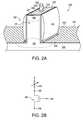
- the vertical FET 100may be used as a selection device such as a memory access device 200 for one or more electrical devices, as illustrated in the structure of FIG. 2A and the schematic diagram of FIG. 2B .
- a memory cell 220is electrically coupled to the vertical FET device 200 .
- the memory cell 220includes a top electrode 222 and a bottom electrode 224 .
- the bottom electrode 224is coupled to a contact 240 for the drain 140 .
- the source 130is coupled to a contact 230 .
- the vertical FET 100is turned “on” and current flows through the channel 125 and memory cell 220 . With appropriate biasing, the current flowing through the memory cell 220 is strong enough to be used as a programming or reset current for the memory cell 220 .
- the memory access device 200 and the memory cells 220are generally formed in an array of access devices 200 and memory cells 220 .
- the source contact 230may extend a relatively long distance from the source 130 of memory access device 200 to the nearest voltage source.
- source contacts 230may be shared by multiple access devices.
- the contacts 230are formed of metal silicide 250 .
- the substrate 555 surface near the bottom of the mesa 120is solicited with metal such as Ni, Co or Ti.
- the metal silicide 250(also known as a salicide) near the bottom of the mesa 120 (or the source metal silicide layer 252 ) acts to reduce the series resistance that results from using a common current source contact for each individual access device 200 in an array.
- the source contacts 230may also be formed of heavily doped silicon as long as the resistance of the doped silicon is low enough to carry the required current.
- the drain contact 240is also formed of a metal silicide 250 which helps to reduce contact resistance between the access device 200 and the bottom electrode 224 of the memory cell 220 .
- the metal silicide 250 formed on the upper portion of the access device 200is the drain metal silicide layer 251 .
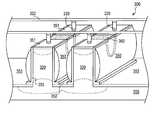
- the access devices 200 and the memory cells 220are arranged in an array 300 as illustrated in FIGS. 3A and 3B .
- a silicon substrate 555is shown. Rising from the silicon substrate 555 are one or more silicon mesas 320 . Each mesa 320 linearly extends in a single direction across the substrate 555 . Multiple mesas 320 are spaced apart from each other and are parallel to each other. In FIGS. 3A and 3B , only two mesas 320 are illustrated for purposes of simplicity. However, many more mesas 320 may be included in array 300 .
- Other substrate and mesa materialsuch as Ge, SiC, GaN, GaAs, InP, graphene and carbon nanotubes, for example, may be used instead of silicon.
- the mesas 320each include source 130 , drain 140 and gate 350 regions.
- the gate 350 regionsare formed on one or more sidewalls of the linearly extended mesas 320 .
- gates 350are formed on two opposite sides of each mesa 320 , thus forming double-gated vertical FETs.
- Single-gated vertical FETsi.e., only one gate 350 on a mesa 320
- surround-gated vertical FETsi.e., mesa 320 is surrounded by a gate 350
- the sidewall gates 350extend along the column of mesas 320 so that each column of mesas 320 includes one or two common sidewall gates 350 .
- the sidewall gates 350may also be solicited.
- the source 130 regions of each mesa 320are commonly shared by each mesa 320 and are electrically coupled with the source metal silicide layer 352 which, as shown in FIG. 3B , covers the surface of the silicon substrate 555 near the mesas 320 . In this way, source 130 regions for multiple mesas 120 are electrically coupled together to form shared sources 130 . Source 130 regions may also merge into a single common source 130 . It is also possible to use a source metal silicide layer 352 that does not cover the entire surface of the silicon substrate 555 near the mesas 320 as long as the source metal silicide layer 352 is still in contact with the sources 130 .
- narrow strips of source metal silicide layer 352could be formed only near the bases of the mesas 320 .
- the drain 140 regionsare electrically coupled to the drain metal silicide layer 351 which covers the upper level of the mesas 320 .
- the gates 350are insulated from the silicide layers 351 , 352 by the thin gate insulator 355 .
- the memory cells 220are electrically coupled via a bottom electrode 224 to the drain metal silicide layer 351 located on the upper surfaces of the mesas 320 .
- the top electrode 222 of each memory cell 220is electrically coupled to a conductor 322 and which may, for example, be formed of metal, and which extends horizontally in a direction perpendicular to the direction that the sidewall gates 350 extend.
- a known interlayer dielectric (“ILD”) material 390for example, silicon oxide, is used to fill-in the gaps between the mesas 320 , substrate 555 and the metal contacts 322 .
- each mesa 320is periodically interrupted by a recess 360 located in between adjacent memory cells 220 .
- the recess 360extends through the drain metal silicide layer 351 and into the mesa 320 .
- the recess 360interrupts the electrically conductive drain metal silicide layer 351 so as to isolate the individual coupling of memory cells 220 to the mesas 320 , thus reducing the occurrence of sneak paths for charge leakage in the array 300 .
- the recess 360is filled with an oxide material such as a spin-on dielectric (“SOD”) silicon oxide or a high density plasma (“HDP”) silicon oxide or some other non-conductive material.
- SODspin-on dielectric
- HDPhigh density plasma
- gate oxide 355does not extend from the recess 360 . Instead, in FIG. 3B , gate 350 directly bounds recess 360 . Other configurations may be used, however. For example, gate oxide 355 could extend across recess 360 and directly bound recess 360 .
- FIG. 3CA simplified top view of the array 300 is illustrated in FIG. 3C .
- the ILD material 390is not shown in the top view.
- each mesa 320and hence each memory cell 220 coupled to a single mesa 320 , share a common source metal silicide layer 352 that extends along the base of each mesa 320 .
- each memory cell 220 coupled to a same mesa 320shares a common gate 350 that also extends along the length of the sidewall of each mesa 320 .
- the upper level of each mesa 320is covered by the drain metal silicide layer 351 , which is periodically interrupted by the recesses 360 .
- Individual memory cells 220are activated (meaning that a desired current flows through the memory cell 220 ) by the appropriate biasing of the source 130 via the respective strip of source metal silicide layer 352 , the respective gate 350 and the respective conductor 322 . While biasing a strip of source metal silicide layer ( 352 or any one of the gates 350 or conductors 322 ) may affect multiple memory cells 220 , activation of a specific memory cell 220 is only accomplished through the appropriate biasing of that cell's connected source metal silicide layer 352 , gate 350 and conductor 322 .
- the occurrence of parasitic resistancesis reduced.
- the source metal silicide layer 352reduces the series resistance that arises from common current source contact to each individual device in the array 300 .
- a drain metal silicide layer 351 on the top surface of each mesa 320the contact resistance between the access device 200 and the bottom electrode 224 of each memory cell 220 is reduced.
- FIG. 4An additional embodiment of a memory array 400 is illustrated in the top view of FIG. 4 .
- the access devices 200 in array 400are formed on mesas 320 as in array 300 .
- the mesas 320have been divided so that gaps 320 exist in the mesas 320 and a single mesa 320 no longer linearly extends as a continuous mesa 320 .
- many mesas 420 of shorter lengthextend in a line across the substrate 555 .
- Gaps 370exist between the shortened mesas 420 within a line 365 .
- Multiple lines of mesas 420are spaced apart from each other and are arranged in parallel with each other.
- Shortened mesas 420 of different lengthscould also be used. For example, three or four memory cells 220 per mesa 420 could be used.
- gaps 370exist between the shortened mesas 420 in a line 365 , the sidewall gates 350 along one or more sides of the mesas 420 in a line still extend continuously for the length of the line 365 , bridging the gaps 370 . Thus, all mesas 420 in a line 365 still share at least one common gate 350 .
- the source metal silicide layer 352 in array 400covers all exposed surfaces of the substrate 555 . This means that the source metal silicide layer 352 covers the substrate 555 surface in strips between lines 365 of mesas 420 as well as in the gaps 370 between mesas 420 in a line 365 , effectively surrounding the bases of each mesa 420 . Additionally, the mesas 420 in adjacent lines 365 may be shifted so that gaps 370 between mesas 420 do not occur in the same linear place for each adjacent line 365 in the array 400 . For example, in the illustration of FIG. 4 , mesas 420 are arranged in a checkerboard-like pattern. Other arrangements are possible depending on the length of the mesas 420 (i.e., the number of memory cells 220 coupled to each mesa 420 ). Aligned or un-shifted mesas 420 may also be used.
- the parasitic resistance in the sourceis reduced.
- the source metal silicide layer 352provides additional current paths, resulting in higher current flow.
- a dedicated contactis not required for any specific strip of source metal silicide layer 352 .
- efficiency of current flow through the source metal silicide layer 352 to a specific mesa 420may be improved.
- a drain metal silicide layer 351 on the top surface of each mesa 420the contact resistance between the access device 200 and the bottom electrode 224 of each memory cell 220 is reduced.
- the silicon mesas 420 of array 400are not limited to being formed of silicon.
- Other materialssuch as Ge, SiC, GaN, GaAs, InP, graphene or carbon nanotubules, for example, may also be used to make the vertical FET devices as well as the underlying substrate.
- double-gated vertical FETsare illustrated, single-gated or surround-gated vertical FETs may also be used, thus providing additional space for a single thicker gate electrode that minimizes resistance.
- all gates on a mesaincluding gates on different sides of a mesa, may be all interconnected, or may be electrically separate.
- Gatesmay be interconnected either at the edge of a memory array or within the array. Additionally, source metal silicide layer 352 may completely cover the substrate near each mesa, or may be arranged in more narrow strips near each mesa. The narrow strips of source metal silicide layer 352 may be electrically interconnected in order to create multiple current paths to an individual mesa, or may be electrically insulated from each other, thus ensuring that a specific narrow strip of source metal silicide layer 352 is used to provide current to a corresponding specific mesa.
- the memory access devices of arrays 300 , 400are able to provide large amounts of current through any selected memory cell 220 .
- access devicesshare common sources 130 because of the source metal silicide layers 352 .
- every mesa 420 in the arrayshares a common source 130 .
- each mesa 320uses a respective source 130 for every memory cell 220 coupled to the mesa 320 .
- the source metal silicide layers 352help to facilitate a larger source current.
- the mesas 320 and the mesas 420 in each line of mesas 420share common gates 350 and drains 140 .
- the multiple current channels 125 available in each line of mesas 320 , 420also increases the amount of current available to be passed through a memory cell 220 .
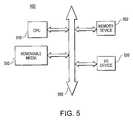
- FIG. 5illustrates a simplified processor system 500 which includes a memory device 502 that includes either array 300 or 400 in accordance with any of the above described embodiments.
- a processor systemsuch as a computer system, generally comprises a central processing unit (CPU) 510 , such as a microprocessor, a digital signal processor, or other programmable digital logic devices, which communicates with an input/output (I/O) device 520 over a bus 590 .
- the memory device 502communicates with the CPU 510 over bus 590 typically through a memory controller.
- the processor system 500may include peripheral devices such as removable media devices 550 (e.g., CD-ROM drive or DVD drive) which communicate with CPU 510 over the bus 590 .
- Memory device 502can be constructed as an integrated circuit, which includes one or more phase change memory devices. If desired, the memory device 502 may be combined with the processor, for example CPU 510 , as a single integrated circuit.
Landscapes
- Semiconductor Memories (AREA)
- Thin Film Transistor (AREA)
Abstract
Description
Claims (26)
Priority Applications (6)
| Application Number | Priority Date | Filing Date | Title |
|---|---|---|---|
| US12/469,563US8274110B2 (en) | 2009-05-20 | 2009-05-20 | Vertically-oriented semiconductor selection device providing high drive current in cross-point array memory |
| KR1020117029810AKR101255956B1 (en) | 2009-05-20 | 2010-05-14 | Vertically-oriented selection transistor structure for cross-point memory array |
| CN201080022032.1ACN102428562B (en) | 2009-05-20 | 2010-05-14 | Vertically-oriented select transistors for cross-point memory arrays |
| PCT/US2010/034840WO2010135172A1 (en) | 2009-05-20 | 2010-05-14 | Vertically-oriented selection transistor structure for cross-point memory array |
| TW099116162ATWI446536B (en) | 2009-05-20 | 2010-05-20 | Vertically-oriented semiconductor selection device for providing high drive current in cross-point array memory |
| US13/605,511US8723252B2 (en) | 2009-05-20 | 2012-09-06 | Vertically-oriented semiconductor selection device providing high drive current in cross-point array memory |
Applications Claiming Priority (1)
| Application Number | Priority Date | Filing Date | Title |
|---|---|---|---|
| US12/469,563US8274110B2 (en) | 2009-05-20 | 2009-05-20 | Vertically-oriented semiconductor selection device providing high drive current in cross-point array memory |
Related Child Applications (1)
| Application Number | Title | Priority Date | Filing Date |
|---|---|---|---|
| US13/605,511ContinuationUS8723252B2 (en) | 2009-05-20 | 2012-09-06 | Vertically-oriented semiconductor selection device providing high drive current in cross-point array memory |
Publications (2)
| Publication Number | Publication Date |
|---|---|
| US20100295120A1 US20100295120A1 (en) | 2010-11-25 |
| US8274110B2true US8274110B2 (en) | 2012-09-25 |
Family
ID=42726080
Family Applications (2)
| Application Number | Title | Priority Date | Filing Date |
|---|---|---|---|
| US12/469,563Active2030-12-11US8274110B2 (en) | 2009-05-20 | 2009-05-20 | Vertically-oriented semiconductor selection device providing high drive current in cross-point array memory |
| US13/605,511Active2029-07-10US8723252B2 (en) | 2009-05-20 | 2012-09-06 | Vertically-oriented semiconductor selection device providing high drive current in cross-point array memory |
Family Applications After (1)
| Application Number | Title | Priority Date | Filing Date |
|---|---|---|---|
| US13/605,511Active2029-07-10US8723252B2 (en) | 2009-05-20 | 2012-09-06 | Vertically-oriented semiconductor selection device providing high drive current in cross-point array memory |
Country Status (5)
| Country | Link |
|---|---|
| US (2) | US8274110B2 (en) |
| KR (1) | KR101255956B1 (en) |
| CN (1) | CN102428562B (en) |
| TW (1) | TWI446536B (en) |
| WO (1) | WO2010135172A1 (en) |
Cited By (15)
| Publication number | Priority date | Publication date | Assignee | Title |
|---|---|---|---|---|
| US20130049120A1 (en)* | 2011-08-23 | 2013-02-28 | Micron Technology, Inc. | Semiconductor device structures including vertical transistor devices, arrays of vertical transistor devices, and methods of fabrication |
| US9240317B2 (en) | 2013-03-28 | 2016-01-19 | Umm Al-Qura University | High temperature GaN based super semiconductor and fabrication process |
| US9299835B1 (en) | 2014-12-04 | 2016-03-29 | International Business Machines Corporation | Vertical field effect transistors |
| US9431305B1 (en) | 2015-12-18 | 2016-08-30 | International Business Machines Corporation | Vertical transistor fabrication and devices |
| US9437503B1 (en) | 2015-12-22 | 2016-09-06 | International Business Machines Corporation | Vertical FETs with variable bottom spacer recess |
| US9530700B1 (en) | 2016-01-28 | 2016-12-27 | International Business Machines Corporation | Method of fabricating vertical field effect transistors with protective fin liner during bottom spacer recess etch |
| US20170345829A1 (en)* | 2016-05-25 | 2017-11-30 | International Business Machines Corporation | High density programmable e-fuse co-integrated with vertical fets |
| US20180130713A1 (en)* | 2016-11-09 | 2018-05-10 | Samsung Electronics Co., Ltd. | Semiconductor devices |
| US10395988B1 (en) | 2018-04-10 | 2019-08-27 | International Business Machines Corporation | Vertical FET transistor with reduced source/drain contact resistance |
| US10658299B2 (en) | 2018-01-05 | 2020-05-19 | International Business Machines Corporation | Replacement metal gate processes for vertical transport field-effect transistor |
| US10672905B2 (en)* | 2018-08-21 | 2020-06-02 | International Business Machines Corporation | Replacement metal gate process for vertical transport field-effect transistor with self-aligned shared contacts |
| US10672670B2 (en)* | 2018-08-21 | 2020-06-02 | International Business Machines Corporation | Replacement metal gate process for vertical transport field-effect transistors with multiple threshold voltages |
| US10714399B2 (en)* | 2018-08-21 | 2020-07-14 | International Business Machines Corporation | Gate-last process for vertical transport field-effect transistor |
| US11081640B2 (en) | 2019-01-02 | 2021-08-03 | International Business Machines Corporation | Magnetic random access memory bottom electrode self-aligned to underlying interconnect structures |
| US12238919B2 (en) | 2020-09-14 | 2025-02-25 | Changxin Memory Technologies, Inc. | Semiconductor structure and semiconductor structure manufacturing method |
Families Citing this family (22)
| Publication number | Priority date | Publication date | Assignee | Title |
|---|---|---|---|---|
| US8853770B2 (en) | 2010-03-16 | 2014-10-07 | Vishay General Semiconductor Llc | Trench MOS device with improved termination structure for high voltage applications |
| KR101841445B1 (en) | 2011-12-06 | 2018-03-23 | 삼성전자주식회사 | Resist RAM device and method of manufacturing the same |
| US20130193400A1 (en)* | 2012-01-27 | 2013-08-01 | Micron Technology, Inc. | Memory Cell Structures and Memory Arrays |
| KR20140109741A (en) | 2013-03-06 | 2014-09-16 | 에스케이하이닉스 주식회사 | Vertical Type Semiconductor Device and Fabrication Method and Operating Method Thereof |
| US9276011B2 (en) | 2013-03-15 | 2016-03-01 | Micron Technology, Inc. | Cell pillar structures and integrated flows |
| US9306063B2 (en)* | 2013-09-27 | 2016-04-05 | Intel Corporation | Vertical transistor devices for embedded memory and logic technologies |
| US9431410B2 (en) | 2013-11-01 | 2016-08-30 | Micron Technology, Inc. | Methods and apparatuses having memory cells including a monolithic semiconductor channel |
| US9437604B2 (en) | 2013-11-01 | 2016-09-06 | Micron Technology, Inc. | Methods and apparatuses having strings of memory cells including a metal source |
| US20150340605A1 (en)* | 2014-05-21 | 2015-11-26 | Kabushiki Kaisha Toshiba | Integrated circuit device |
| KR102472673B1 (en) | 2016-03-21 | 2022-11-30 | 삼성전자주식회사 | Semiconductor device and method for manufacturing the same |
| EP3676878A4 (en) | 2017-08-31 | 2020-11-04 | Micron Technology, Inc. | SEMICONDUCTOR COMPONENTS, HYBRID TRANSISTORS AND RELATED PROCESSES |
| CN111052395A (en) | 2017-08-31 | 2020-04-21 | 美光科技公司 | Semiconductor device, transistor and related method for contacting metal oxide semiconductor device |
| WO2019209330A1 (en) | 2018-04-27 | 2019-10-31 | Hewlett Packard Enterprise Development Lp | Vertical jfet device for memristor array interface |
| US10504794B1 (en)* | 2018-06-25 | 2019-12-10 | International Business Machines Corporation | Self-aligned silicide/germanide formation to reduce external resistance in a vertical field-effect transistor |
| EP3667733A1 (en)* | 2018-12-13 | 2020-06-17 | IMEC vzw | Silicided fin junction for back-side connection |
| CN111146237B (en)* | 2019-12-18 | 2023-09-26 | 上海集成电路研发中心有限公司 | Resistive random access memory unit structure and preparation method |
| US11145816B2 (en) | 2019-12-20 | 2021-10-12 | International Business Machines Corporation | Resistive random access memory cells integrated with vertical field effect transistor |
| CN114188320A (en) | 2020-09-14 | 2022-03-15 | 长鑫存储技术有限公司 | Semiconductor structure and method of manufacturing the semiconductor structure |
| CN113611667B (en)* | 2021-07-02 | 2024-09-10 | 芯盟科技有限公司 | Transistor array and manufacturing method thereof, semiconductor device and manufacturing method thereof |
| CN113611666B (en)* | 2021-07-02 | 2024-09-10 | 芯盟科技有限公司 | Transistor array and manufacturing method thereof, semiconductor device and manufacturing method thereof |
| CN113611665B (en)* | 2021-07-02 | 2024-08-02 | 芯盟科技有限公司 | Transistor array and manufacturing method thereof, semiconductor device and manufacturing method thereof |
| CN115995421B (en)* | 2023-03-23 | 2023-05-23 | 江西兆驰半导体有限公司 | LED chip sorting method |
Citations (17)
| Publication number | Priority date | Publication date | Assignee | Title |
|---|---|---|---|---|
| US5107321A (en) | 1990-04-02 | 1992-04-21 | National Semiconductor Corporation | Interconnect method for semiconductor devices |
| US5824577A (en) | 1995-02-16 | 1998-10-20 | National Semiconductor Corporation | MOSFET with reduced leakage current |
| US5899735A (en) | 1997-09-19 | 1999-05-04 | Vanguard International Semiconductor Corporation | Method for making low-resistance contacts between polysilicon and metal silicide on semiconductor integrated circuits |
| US5918141A (en)* | 1997-06-20 | 1999-06-29 | National Semiconductor Corporation | Method of masking silicide deposition utilizing a photoresist mask |
| US6165826A (en) | 1994-12-23 | 2000-12-26 | Intel Corporation | Transistor with low resistance tip and method of fabrication in a CMOS process |
| US6218276B1 (en) | 1997-12-22 | 2001-04-17 | Lsi Logic Corporation | Silicide encapsulation of polysilicon gate and interconnect |
| US6300198B1 (en) | 1997-03-19 | 2001-10-09 | Siemens Aktiengesellschaft | Method for producing a vertical MOS-transistor |
| US6677204B2 (en)* | 2000-08-14 | 2004-01-13 | Matrix Semiconductor, Inc. | Multigate semiconductor device with vertical channel current and method of fabrication |
| US20040157353A1 (en)* | 2001-03-13 | 2004-08-12 | International Business Machines Corporation | Ultra scalable high speed heterojunction vertical n-channel MISFETs and methods thereof |
| WO2005079182A2 (en) | 2004-01-22 | 2005-09-01 | International Business Machines Corporation | Vertical fin-fet mos devices |
| US6940113B2 (en) | 2001-06-28 | 2005-09-06 | Sharp Laboratories Of America, Inc. | Trench isolated cross-point memory array |
| US20060017088A1 (en) | 2004-07-20 | 2006-01-26 | Abbott Todd R | DRAM layout with vertical FETS and method of formation |
| US20080035958A1 (en)* | 2006-08-09 | 2008-02-14 | Yoshiaki Asao | Magnetic random access memory |
| US20080049486A1 (en) | 2006-08-28 | 2008-02-28 | Qimonda Ag | Transistor, memory cell array and method for forming and operating a memory device |
| US20080099814A1 (en) | 2006-10-30 | 2008-05-01 | Qimonda Ag | Integrated circuit and method for production |
| US20090166703A1 (en)* | 2008-01-02 | 2009-07-02 | Nanya Technology Corporation | Memory device with a length-controllable channel |
| US20100295119A1 (en)* | 2009-05-20 | 2010-11-25 | Gurtej Sandhu | Vertically-oriented semiconductor selection device for cross-point array memory |
Family Cites Families (2)
| Publication number | Priority date | Publication date | Assignee | Title |
|---|---|---|---|---|
| US5460988A (en)* | 1994-04-25 | 1995-10-24 | United Microelectronics Corporation | Process for high density flash EPROM cell |
| US5885864A (en)* | 1996-10-24 | 1999-03-23 | Micron Technology, Inc. | Method for forming compact memory cell using vertical devices |
- 2009
- 2009-05-20USUS12/469,563patent/US8274110B2/enactiveActive
- 2010
- 2010-05-14CNCN201080022032.1Apatent/CN102428562B/enactiveActive
- 2010-05-14WOPCT/US2010/034840patent/WO2010135172A1/enactiveApplication Filing
- 2010-05-14KRKR1020117029810Apatent/KR101255956B1/enactiveActive
- 2010-05-20TWTW099116162Apatent/TWI446536B/enactive
- 2012
- 2012-09-06USUS13/605,511patent/US8723252B2/enactiveActive
Patent Citations (18)
| Publication number | Priority date | Publication date | Assignee | Title |
|---|---|---|---|---|
| US5107321A (en) | 1990-04-02 | 1992-04-21 | National Semiconductor Corporation | Interconnect method for semiconductor devices |
| US6165826A (en) | 1994-12-23 | 2000-12-26 | Intel Corporation | Transistor with low resistance tip and method of fabrication in a CMOS process |
| US5824577A (en) | 1995-02-16 | 1998-10-20 | National Semiconductor Corporation | MOSFET with reduced leakage current |
| US6300198B1 (en) | 1997-03-19 | 2001-10-09 | Siemens Aktiengesellschaft | Method for producing a vertical MOS-transistor |
| US5918141A (en)* | 1997-06-20 | 1999-06-29 | National Semiconductor Corporation | Method of masking silicide deposition utilizing a photoresist mask |
| US5899735A (en) | 1997-09-19 | 1999-05-04 | Vanguard International Semiconductor Corporation | Method for making low-resistance contacts between polysilicon and metal silicide on semiconductor integrated circuits |
| US6218276B1 (en) | 1997-12-22 | 2001-04-17 | Lsi Logic Corporation | Silicide encapsulation of polysilicon gate and interconnect |
| US6677204B2 (en)* | 2000-08-14 | 2004-01-13 | Matrix Semiconductor, Inc. | Multigate semiconductor device with vertical channel current and method of fabrication |
| US20040157353A1 (en)* | 2001-03-13 | 2004-08-12 | International Business Machines Corporation | Ultra scalable high speed heterojunction vertical n-channel MISFETs and methods thereof |
| US6940113B2 (en) | 2001-06-28 | 2005-09-06 | Sharp Laboratories Of America, Inc. | Trench isolated cross-point memory array |
| WO2005079182A2 (en) | 2004-01-22 | 2005-09-01 | International Business Machines Corporation | Vertical fin-fet mos devices |
| US20060017088A1 (en) | 2004-07-20 | 2006-01-26 | Abbott Todd R | DRAM layout with vertical FETS and method of formation |
| US20080035958A1 (en)* | 2006-08-09 | 2008-02-14 | Yoshiaki Asao | Magnetic random access memory |
| US20080049486A1 (en) | 2006-08-28 | 2008-02-28 | Qimonda Ag | Transistor, memory cell array and method for forming and operating a memory device |
| US20080099814A1 (en) | 2006-10-30 | 2008-05-01 | Qimonda Ag | Integrated circuit and method for production |
| US20090166703A1 (en)* | 2008-01-02 | 2009-07-02 | Nanya Technology Corporation | Memory device with a length-controllable channel |
| US20100295119A1 (en)* | 2009-05-20 | 2010-11-25 | Gurtej Sandhu | Vertically-oriented semiconductor selection device for cross-point array memory |
| US8076717B2 (en)* | 2009-05-20 | 2011-12-13 | Micron Technology, Inc. | Vertically-oriented semiconductor selection device for cross-point array memory |
Cited By (47)
| Publication number | Priority date | Publication date | Assignee | Title |
|---|---|---|---|---|
| US10002935B2 (en)* | 2011-08-23 | 2018-06-19 | Micron Technology, Inc. | Semiconductor devices and structures and methods of formation |
| US8969154B2 (en)* | 2011-08-23 | 2015-03-03 | Micron Technology, Inc. | Methods for fabricating semiconductor device structures and arrays of vertical transistor devices |
| US11652173B2 (en)* | 2011-08-23 | 2023-05-16 | Micron Technology, Inc. | Methods of forming a semiconductor device comprising a channel material |
| US9356155B2 (en) | 2011-08-23 | 2016-05-31 | Micron Technology, Inc. | Semiconductor device structures and arrays of vertical transistor devices |
| US20210273111A1 (en)* | 2011-08-23 | 2021-09-02 | Micron Technology, Inc. | Methods of forming a semiconductor device comprising a channel material |
| US11011647B2 (en)* | 2011-08-23 | 2021-05-18 | Micron Technology, Inc. | Semiconductor devices comprising channel materials |
| US20160276454A1 (en)* | 2011-08-23 | 2016-09-22 | Micron Technology, Inc. | Semiconductor devices and structures and methods of formation |
| US20200027990A1 (en)* | 2011-08-23 | 2020-01-23 | Micron Technology, Inc. | Semiconductor devices comprising channel materials |
| US10446692B2 (en)* | 2011-08-23 | 2019-10-15 | Micron Technology, Inc. | Semiconductor devices and structures |
| US20130049120A1 (en)* | 2011-08-23 | 2013-02-28 | Micron Technology, Inc. | Semiconductor device structures including vertical transistor devices, arrays of vertical transistor devices, and methods of fabrication |
| US20180301539A1 (en)* | 2011-08-23 | 2018-10-18 | Micron Technology, Inc. | Semiconductor devices and structures and methods of formation |
| US9240317B2 (en) | 2013-03-28 | 2016-01-19 | Umm Al-Qura University | High temperature GaN based super semiconductor and fabrication process |
| US10332801B2 (en) | 2014-12-04 | 2019-06-25 | International Business Machines Corporation | Vertical field effect transistors |
| US9570357B2 (en) | 2014-12-04 | 2017-02-14 | International Business Machines Corporation | Vertical field effect transistors |
| US9299835B1 (en) | 2014-12-04 | 2016-03-29 | International Business Machines Corporation | Vertical field effect transistors |
| US11024546B2 (en) | 2014-12-04 | 2021-06-01 | International Business Machines Corporation | Vertical field effect transistors |
| US10943831B2 (en) | 2014-12-04 | 2021-03-09 | International Business Machines Corporation | Vertical field effect transistors |
| US10896857B2 (en) | 2014-12-04 | 2021-01-19 | International Business Machines Corporation | Vertical field effect transistors |
| US10043715B2 (en) | 2014-12-04 | 2018-08-07 | International Business Machines Corporation | Vertical field effect transistors |
| US9653360B2 (en) | 2014-12-04 | 2017-05-16 | International Business Machines Corporation | Vertical field effect transistors |
| US10529627B2 (en) | 2014-12-04 | 2020-01-07 | International Business Machines Corporation | Vertical field effect transistors |
| US10622459B2 (en) | 2015-12-18 | 2020-04-14 | International Business Machines Corporation | Vertical transistor fabrication and devices |
| US10727316B2 (en) | 2015-12-18 | 2020-07-28 | International Business Machines Corporation | Vertical transistor fabrication and devices |
| US10388757B2 (en) | 2015-12-18 | 2019-08-20 | International Business Machines Corporation | Vertical transistor fabrication and devices |
| US9941411B2 (en) | 2015-12-18 | 2018-04-10 | International Business Machines Corporation | Vertical transistor fabrication and devices |
| US9431305B1 (en) | 2015-12-18 | 2016-08-30 | International Business Machines Corporation | Vertical transistor fabrication and devices |
| US9985115B2 (en) | 2015-12-18 | 2018-05-29 | International Business Machines Corporation | Vertical transistor fabrication and devices |
| US9793374B2 (en) | 2015-12-18 | 2017-10-17 | International Business Machines Corporation | Vertical transistor fabrication and devices |
| US9437503B1 (en) | 2015-12-22 | 2016-09-06 | International Business Machines Corporation | Vertical FETs with variable bottom spacer recess |
| US9530700B1 (en) | 2016-01-28 | 2016-12-27 | International Business Machines Corporation | Method of fabricating vertical field effect transistors with protective fin liner during bottom spacer recess etch |
| US9601491B1 (en)* | 2016-01-28 | 2017-03-21 | International Business Machines Corporation | Vertical field effect transistors having epitaxial fin channel with spacers below gate structure |
| US10164119B2 (en) | 2016-01-28 | 2018-12-25 | International Business Machines Corporation | Vertical field effect transistors with protective fin liner during bottom spacer recess etch |
| US10109535B2 (en) | 2016-01-28 | 2018-10-23 | International Business Machines Corporation | Method of fabricating vertical field effect transistors with protective fin liner during bottom spacer recess ETCH |
| US20170345829A1 (en)* | 2016-05-25 | 2017-11-30 | International Business Machines Corporation | High density programmable e-fuse co-integrated with vertical fets |
| US10438956B2 (en)* | 2016-05-25 | 2019-10-08 | International Business Machines Corporation | High density programmable e-fuse co-integrated with vertical FETs |
| US20180130713A1 (en)* | 2016-11-09 | 2018-05-10 | Samsung Electronics Co., Ltd. | Semiconductor devices |
| US10937700B2 (en)* | 2016-11-09 | 2021-03-02 | Samsung Electronics Co., Ltd. | Semiconductor devices |
| US10658299B2 (en) | 2018-01-05 | 2020-05-19 | International Business Machines Corporation | Replacement metal gate processes for vertical transport field-effect transistor |
| US10395988B1 (en) | 2018-04-10 | 2019-08-27 | International Business Machines Corporation | Vertical FET transistor with reduced source/drain contact resistance |
| US11257721B2 (en) | 2018-08-21 | 2022-02-22 | International Business Machines Corporation | Replacement metal gate process for vertical transport field-effect transistors with multiple threshold voltages |
| US10672905B2 (en)* | 2018-08-21 | 2020-06-02 | International Business Machines Corporation | Replacement metal gate process for vertical transport field-effect transistor with self-aligned shared contacts |
| US11145555B2 (en)* | 2018-08-21 | 2021-10-12 | International Business Machines Corporation | Gate-last process for vertical transport field-effect transistor |
| US10672670B2 (en)* | 2018-08-21 | 2020-06-02 | International Business Machines Corporation | Replacement metal gate process for vertical transport field-effect transistors with multiple threshold voltages |
| US11271106B2 (en)* | 2018-08-21 | 2022-03-08 | International Business Machines Corporation | Replacement metal gate process for vertical transport field-effect transistor with self-aligned shared contacts |
| US10714399B2 (en)* | 2018-08-21 | 2020-07-14 | International Business Machines Corporation | Gate-last process for vertical transport field-effect transistor |
| US11081640B2 (en) | 2019-01-02 | 2021-08-03 | International Business Machines Corporation | Magnetic random access memory bottom electrode self-aligned to underlying interconnect structures |
| US12238919B2 (en) | 2020-09-14 | 2025-02-25 | Changxin Memory Technologies, Inc. | Semiconductor structure and semiconductor structure manufacturing method |
Also Published As
| Publication number | Publication date |
|---|---|
| US20100295120A1 (en) | 2010-11-25 |
| TWI446536B (en) | 2014-07-21 |
| WO2010135172A1 (en) | 2010-11-25 |
| CN102428562B (en) | 2014-11-05 |
| KR20120011890A (en) | 2012-02-08 |
| KR101255956B1 (en) | 2013-04-23 |
| TW201110348A (en) | 2011-03-16 |
| US8723252B2 (en) | 2014-05-13 |
| US20120326242A1 (en) | 2012-12-27 |
| CN102428562A (en) | 2012-04-25 |
Similar Documents
| Publication | Publication Date | Title |
|---|---|---|
| US8274110B2 (en) | Vertically-oriented semiconductor selection device providing high drive current in cross-point array memory | |
| US8076717B2 (en) | Vertically-oriented semiconductor selection device for cross-point array memory | |
| US8648428B2 (en) | Memory cell array with semiconductor selection device for multiple memory cells | |
| US9698202B2 (en) | Parallel bit line three-dimensional resistive random access memory | |
| JP6280229B2 (en) | Field effect transistor structure and memory array | |
| US8878271B2 (en) | Vertical access device and apparatuses having a body connection line, and related method of operating the same | |
| US8890108B2 (en) | Memory device having vertical selection transistors with shared channel structure and method for making the same | |
| US20090034355A1 (en) | Integrated circuit including memory cells with tunnel fet as selection transistor | |
| US20080203469A1 (en) | Integrated circuit including an array of memory cells having dual gate transistors | |
| US8395139B1 (en) | 1T1R resistive memory device and fabrication method thereof | |
| EP2641248B1 (en) | Transistor driven 3d memory | |
| US12382642B1 (en) | Nonvolatile memory device including dual memory layers | |
| TW499678B (en) | Semiconductor-memory with a memory-cell-array | |
| US20240138153A1 (en) | Ferroelectric memory device and memory array |
Legal Events
| Date | Code | Title | Description |
|---|---|---|---|
| AS | Assignment | Owner name:MICRON TECHNOLOGY, INC., IDAHO Free format text:ASSIGNMENT OF ASSIGNORS INTEREST;ASSIGNORS:SANDHU, GURTEJ;ZAHURAK, JOHN K.;PARKS, JAY;SIGNING DATES FROM 20090508 TO 20090515;REEL/FRAME:022715/0192 | |
| FEPP | Fee payment procedure | Free format text:PAYOR NUMBER ASSIGNED (ORIGINAL EVENT CODE: ASPN); ENTITY STATUS OF PATENT OWNER: LARGE ENTITY | |
| STCF | Information on status: patent grant | Free format text:PATENTED CASE | |
| FPAY | Fee payment | Year of fee payment:4 | |
| AS | Assignment | Owner name:U.S. BANK NATIONAL ASSOCIATION, AS COLLATERAL AGENT, CALIFORNIA Free format text:SECURITY INTEREST;ASSIGNOR:MICRON TECHNOLOGY, INC.;REEL/FRAME:038669/0001 Effective date:20160426 Owner name:U.S. BANK NATIONAL ASSOCIATION, AS COLLATERAL AGEN Free format text:SECURITY INTEREST;ASSIGNOR:MICRON TECHNOLOGY, INC.;REEL/FRAME:038669/0001 Effective date:20160426 | |
| AS | Assignment | Owner name:MORGAN STANLEY SENIOR FUNDING, INC., AS COLLATERAL AGENT, MARYLAND Free format text:PATENT SECURITY AGREEMENT;ASSIGNOR:MICRON TECHNOLOGY, INC.;REEL/FRAME:038954/0001 Effective date:20160426 Owner name:MORGAN STANLEY SENIOR FUNDING, INC., AS COLLATERAL Free format text:PATENT SECURITY AGREEMENT;ASSIGNOR:MICRON TECHNOLOGY, INC.;REEL/FRAME:038954/0001 Effective date:20160426 | |
| AS | Assignment | Owner name:U.S. BANK NATIONAL ASSOCIATION, AS COLLATERAL AGENT, CALIFORNIA Free format text:CORRECTIVE ASSIGNMENT TO CORRECT THE REPLACE ERRONEOUSLY FILED PATENT #7358718 WITH THE CORRECT PATENT #7358178 PREVIOUSLY RECORDED ON REEL 038669 FRAME 0001. ASSIGNOR(S) HEREBY CONFIRMS THE SECURITY INTEREST;ASSIGNOR:MICRON TECHNOLOGY, INC.;REEL/FRAME:043079/0001 Effective date:20160426 Owner name:U.S. BANK NATIONAL ASSOCIATION, AS COLLATERAL AGEN Free format text:CORRECTIVE ASSIGNMENT TO CORRECT THE REPLACE ERRONEOUSLY FILED PATENT #7358718 WITH THE CORRECT PATENT #7358178 PREVIOUSLY RECORDED ON REEL 038669 FRAME 0001. ASSIGNOR(S) HEREBY CONFIRMS THE SECURITY INTEREST;ASSIGNOR:MICRON TECHNOLOGY, INC.;REEL/FRAME:043079/0001 Effective date:20160426 | |
| AS | Assignment | Owner name:JPMORGAN CHASE BANK, N.A., AS COLLATERAL AGENT, ILLINOIS Free format text:SECURITY INTEREST;ASSIGNORS:MICRON TECHNOLOGY, INC.;MICRON SEMICONDUCTOR PRODUCTS, INC.;REEL/FRAME:047540/0001 Effective date:20180703 Owner name:JPMORGAN CHASE BANK, N.A., AS COLLATERAL AGENT, IL Free format text:SECURITY INTEREST;ASSIGNORS:MICRON TECHNOLOGY, INC.;MICRON SEMICONDUCTOR PRODUCTS, INC.;REEL/FRAME:047540/0001 Effective date:20180703 | |
| AS | Assignment | Owner name:MICRON TECHNOLOGY, INC., IDAHO Free format text:RELEASE BY SECURED PARTY;ASSIGNOR:U.S. BANK NATIONAL ASSOCIATION, AS COLLATERAL AGENT;REEL/FRAME:047243/0001 Effective date:20180629 | |
| AS | Assignment | Owner name:MICRON TECHNOLOGY, INC., IDAHO Free format text:RELEASE BY SECURED PARTY;ASSIGNOR:MORGAN STANLEY SENIOR FUNDING, INC., AS COLLATERAL AGENT;REEL/FRAME:050937/0001 Effective date:20190731 | |
| AS | Assignment | Owner name:MICRON SEMICONDUCTOR PRODUCTS, INC., IDAHO Free format text:RELEASE BY SECURED PARTY;ASSIGNOR:JPMORGAN CHASE BANK, N.A., AS COLLATERAL AGENT;REEL/FRAME:051028/0001 Effective date:20190731 Owner name:MICRON TECHNOLOGY, INC., IDAHO Free format text:RELEASE BY SECURED PARTY;ASSIGNOR:JPMORGAN CHASE BANK, N.A., AS COLLATERAL AGENT;REEL/FRAME:051028/0001 Effective date:20190731 | |
| MAFP | Maintenance fee payment | Free format text:PAYMENT OF MAINTENANCE FEE, 8TH YEAR, LARGE ENTITY (ORIGINAL EVENT CODE: M1552); ENTITY STATUS OF PATENT OWNER: LARGE ENTITY Year of fee payment:8 | |
| MAFP | Maintenance fee payment | Free format text:PAYMENT OF MAINTENANCE FEE, 12TH YEAR, LARGE ENTITY (ORIGINAL EVENT CODE: M1553); ENTITY STATUS OF PATENT OWNER: LARGE ENTITY Year of fee payment:12 |