US8272770B2 - TIR switched flat panel display - Google Patents
TIR switched flat panel displayDownload PDFInfo
- Publication number
- US8272770B2 US8272770B2US12/319,171US31917109AUS8272770B2US 8272770 B2US8272770 B2US 8272770B2US 31917109 AUS31917109 AUS 31917109AUS 8272770 B2US8272770 B2US 8272770B2
- Authority
- US
- United States
- Prior art keywords
- light
- display device
- light guide
- output
- mask plate
- Prior art date
- Legal status (The legal status is an assumption and is not a legal conclusion. Google has not performed a legal analysis and makes no representation as to the accuracy of the status listed.)
- Expired - Fee Related, expires
Links
- 239000000463materialSubstances0.000claimsdescription34
- 230000003287optical effectEffects0.000claimsdescription23
- 238000000605extractionMethods0.000claims4
- 239000011358absorbing materialSubstances0.000claims3
- 239000003086colorantSubstances0.000abstractdescription14
- 238000005516engineering processMethods0.000description35
- 125000006850spacer groupChemical group0.000description20
- 230000008901benefitEffects0.000description8
- 239000000758substrateSubstances0.000description6
- 238000009792diffusion processMethods0.000description5
- 238000000034methodMethods0.000description5
- 238000009125cardiac resynchronization therapyMethods0.000description4
- 230000008859changeEffects0.000description4
- 239000004020conductorSubstances0.000description4
- 230000000694effectsEffects0.000description4
- 239000000284extractSubstances0.000description4
- 238000004519manufacturing processMethods0.000description4
- 239000000853adhesiveSubstances0.000description3
- 230000001070adhesive effectEffects0.000description3
- 230000007812deficiencyEffects0.000description3
- 230000033001locomotionEffects0.000description3
- 239000011159matrix materialSubstances0.000description3
- 239000012528membraneSubstances0.000description3
- QSHDDOUJBYECFT-UHFFFAOYSA-NmercuryChemical compound[Hg]QSHDDOUJBYECFT-UHFFFAOYSA-N0.000description3
- 229910052753mercuryInorganic materials0.000description3
- 230000008569processEffects0.000description3
- 239000011800void materialSubstances0.000description3
- NIXOWILDQLNWCW-UHFFFAOYSA-Nacrylic acid groupChemical groupC(C=C)(=O)ONIXOWILDQLNWCW-UHFFFAOYSA-N0.000description2
- 230000009286beneficial effectEffects0.000description2
- 230000005540biological transmissionEffects0.000description2
- 230000001413cellular effectEffects0.000description2
- 239000012141concentrateSubstances0.000description2
- 230000001419dependent effectEffects0.000description2
- 238000013461designMethods0.000description2
- 229920001971elastomerPolymers0.000description2
- 239000000806elastomerSubstances0.000description2
- 239000011521glassSubstances0.000description2
- 230000006872improvementEffects0.000description2
- 239000004973liquid crystal related substanceSubstances0.000description2
- 230000007246mechanismEffects0.000description2
- 230000010076replicationEffects0.000description2
- VYZAMTAEIAYCRO-UHFFFAOYSA-NChromiumChemical compound[Cr]VYZAMTAEIAYCRO-UHFFFAOYSA-N0.000description1
- 241000219492QuercusSpecies0.000description1
- 235000010724Wisteria floribundaNutrition0.000description1
- 238000010521absorption reactionMethods0.000description1
- 230000004075alterationEffects0.000description1
- 229910052782aluminiumInorganic materials0.000description1
- XAGFODPZIPBFFR-UHFFFAOYSA-NaluminiumChemical compound[Al]XAGFODPZIPBFFR-UHFFFAOYSA-N0.000description1
- 238000013459approachMethods0.000description1
- 238000003491arrayMethods0.000description1
- 238000005452bendingMethods0.000description1
- 239000003990capacitorSubstances0.000description1
- 239000006229carbon blackSubstances0.000description1
- 239000011248coating agentSubstances0.000description1
- 238000000576coating methodMethods0.000description1
- 238000004891communicationMethods0.000description1
- 238000001816coolingMethods0.000description1
- 230000007547defectEffects0.000description1
- 238000010586diagramMethods0.000description1
- 239000013013elastic materialSubstances0.000description1
- 238000005265energy consumptionMethods0.000description1
- 230000007613environmental effectEffects0.000description1
- 239000011152fibreglassSubstances0.000description1
- 238000001914filtrationMethods0.000description1
- 235000013305foodNutrition0.000description1
- 239000011810insulating materialSubstances0.000description1
- 230000001788irregularEffects0.000description1
- 230000005389magnetismEffects0.000description1
- 230000013011matingEffects0.000description1
- 229910052751metalInorganic materials0.000description1
- 239000002184metalSubstances0.000description1
- 238000012986modificationMethods0.000description1
- 230000004048modificationEffects0.000description1
- 238000000465mouldingMethods0.000description1
- 239000011368organic materialSubstances0.000description1
- 239000002245particleSubstances0.000description1
- 239000011295pitchSubstances0.000description1
- 239000004033plasticSubstances0.000description1
- 230000010287polarizationEffects0.000description1
- 229920000515polycarbonatePolymers0.000description1
- 239000004417polycarbonateSubstances0.000description1
- 229920000728polyesterPolymers0.000description1
- 230000009467reductionEffects0.000description1
- 238000012163sequencing techniqueMethods0.000description1
- 239000010703siliconSubstances0.000description1
- 229910052710siliconInorganic materials0.000description1
- 229910052709silverInorganic materials0.000description1
- 239000004332silverSubstances0.000description1
- 239000011343solid materialSubstances0.000description1
- 238000001228spectrumMethods0.000description1
Images


Classifications
- G—PHYSICS
- G09—EDUCATION; CRYPTOGRAPHY; DISPLAY; ADVERTISING; SEALS
- G09F—DISPLAYING; ADVERTISING; SIGNS; LABELS OR NAME-PLATES; SEALS
- G09F9/00—Indicating arrangements for variable information in which the information is built-up on a support by selection or combination of individual elements
- G09F9/30—Indicating arrangements for variable information in which the information is built-up on a support by selection or combination of individual elements in which the desired character or characters are formed by combining individual elements
- G—PHYSICS
- G02—OPTICS
- G02B—OPTICAL ELEMENTS, SYSTEMS OR APPARATUS
- G02B6/00—Light guides; Structural details of arrangements comprising light guides and other optical elements, e.g. couplings
- G02B6/0001—Light guides; Structural details of arrangements comprising light guides and other optical elements, e.g. couplings specially adapted for lighting devices or systems
- G02B6/0011—Light guides; Structural details of arrangements comprising light guides and other optical elements, e.g. couplings specially adapted for lighting devices or systems the light guides being planar or of plate-like form
- G02B6/0033—Means for improving the coupling-out of light from the light guide
- G02B6/005—Means for improving the coupling-out of light from the light guide provided by one optical element, or plurality thereof, placed on the light output side of the light guide
- G—PHYSICS
- G02—OPTICS
- G02B—OPTICAL ELEMENTS, SYSTEMS OR APPARATUS
- G02B6/00—Light guides; Structural details of arrangements comprising light guides and other optical elements, e.g. couplings
- G02B6/24—Coupling light guides
- G02B6/26—Optical coupling means
- G02B6/35—Optical coupling means having switching means
- G02B6/351—Optical coupling means having switching means involving stationary waveguides with moving interposed optical elements
- G02B6/3522—Optical coupling means having switching means involving stationary waveguides with moving interposed optical elements the optical element enabling or impairing total internal reflection
Definitions
- This inventionrelates generally to light display devices, and more particularly is a flat panel display in which the light is switched by enabling and disabling total internal reflection (TIR), and in which the switched light is directed by optics.
- TIRtotal internal reflection
- LCDsLiquid crystal displays
- plasma technologyAnother, less common technology used for flat panel displays is plasma technology.
- Other known display technologies used in thicker flat panel displaysare of the rear projection type. For very large displays, discrete arrays of LEDs are the dominant technology.
- CRT type displaysthat used to be the dominant technology, have almost vanished even though the performance of the newer technologies is not significantly greater than CRT.
- Some current art LCD displaysstill cannot match the refresh rate of CRTs.
- a first shortcoming of LCD display technologyis the high energy consumption.
- a 65′′ diagonal HDTV LCD TVtypically draws around a half of a kilowatt. This is a result of the poor efficiency of the technology.
- LCDsneed polarized light to function. However, approximately half of the light generated by the backlight is absorbed in the creation of polarized light. Many inventions have been devised to reduce this loss. In reality, little real improvement has been realized by manufactures due to cost or the reduction in other performance parameters.
- One product that is designed to recycle light not having the correct polarizationis called “DBEF” and is manufactured by 3M of Minneapolis, Minn.
- red, green, and blue filtersare used to create colors. These filters do not reflect unused light, but rather absorb it. For example: red filters absorb the green and blue light while only letting red light pass through. In theory, a perfect blue filter would let 33% of the light through. In reality filter materials perform significantly less than the theoretical 33%.
- Another place where light is absorbedis in the matrix between the color filters. This matrix area is required for circuitry and transistors used to control the pixels. The required area is significant in that one pixel requires three transistors, one transistor being required for each of the three colors. Also, additional circuitry is required to drive the transistors. The matrix area between the filters may absorb approximately half the overall light available.
- an LCD panelmay only be 8% efficient when all of the pixels are on.
- an imagehas approximately one half of the pixels turned on when creating an image, and with the half of the pixels that are off absorbing rather than reflecting, the resulting LCD efficiency is only in the 4% range.
- the quality of the colors from a LCD displayare limited by the wavelengths of light emitted from the light source and the properties of the color filters used in the display. Both of these factors result in displays that cannot accurately reproduce colors found in nature.
- LCD technologyAnother deficiency with LCD technology is their limited environmental operating range.
- the liquid crystal materialdoesn't function well at high and low temperatures. Displays that are used in extreme environments are often cooled or heated to keep them within a moderate operating range.
- Another problem with using LCDs in non-optimal environmentis that the polarizing films required for LCD displays degrade when exposed to high humidity. Measures must be taken to reduce the effect of this property. In displays that are used in extreme environments the displays and their polarizing films are encased in glass windows.
- Plasma thin panel displaysare the typical technology of choice for large screen TVs.
- the plasma displaysalso consume a significant amount of power.
- Plasma TVsdo not last as long as LCD TVs and experience “burn in”. Burn in occurs when the on pixels remain on for a long period of time. These pixels lose their strength and become washed out over time. Cost is another issue with plasma technology.
- the projectorIn TV applications the projector is often deployed in a rear projection configuration.
- the front projection modeis more commonly used.
- MEMS mirror arrayin disclosed in each of U.S. Pat. Nos. 4,566,935; 4,596,992; 4,615,595; 4,662,746; 4,710,732; 4,956,619; and 5,028,939; all by inventor Larry Hornbeck of Texas, and assigned to Texas Instruments (TI) of Texas.
- the TI technologyuses an array of MEMS mirrors that change their incidence angle to the light path to switch the light from an off position to an on position. When the mirror is in the on position, the mirror reflects the light through the optical path. When the mirror is in the off position, the light is reflected to a path that falls outside the projection optics. This in effect turns the light valve to an off state.
- the light transmissionis less than 70%.
- To allow for the change of angular orientation of the mirrorsthere must be a substantial space between adjacent mirrors. The required gap causes a lot of light to be wasted. Further, the reflected light is absorbed into the light valve. The absorbed energy makes cooling the switching devices that use this technology a challenge.
- U.S. Pat. No. 6,421,103by Akira Yamaguchi of Japan and assigned to Fuji Film, discloses a backlight for use with LCD panels.
- This patentdiscloses light sources, a substrate, apertures (not used as a light guide), and reflective regions on the substrate. The light is either reflected by the reflective surface or passes through the apertures. The light that passes through the apertures is captured by a lens and is used to control the direction of the light.
- the Yamaguchi referenceteaches a restricted angle of the light to concentrate more light directly at the viewer of an LCD type display.
- U.S. Pat. No. 5,396,350by Karl Beeson of Princeton, N.J., discloses a light guide with optical elements that are used to extract light from the light guide.
- the optical elementsare on the viewer's side of the panel and have limited ability to control the direction of the light.
- This inventionis intended to be used in conjunction with an LCD type panel to concentrate light towards the viewer.
- the present inventionis a light valve for use in thin flat panel displays.
- Flat panel displaysare used in cellular phones, laptop computers, computer monitors, TVs, and commercial displays.
- the light valve of the present inventioneither extracts light or allows light to travel up a light guide through the TIR process.
- Lightis initially injected into the light guide from the edges of the light guide. Light then travels up the light guide by reflecting off of the inside surfaces of the light guide. If the light reaches the top of the light guide, reflective material reflects the light back toward the bottom of the light guide.
- the lightwill typically find a point where an element of the TIR switch is in an on position, in contact with the light guide.
- a switch elementcontacts the light guide, light is extracted from the light guide and is directed to an optic system that redirects the light to the viewer.
- Switch elements that are not in contact with the surface of the light guidedo not extract light. Contacting switches create an “on” pixel, while a switch not in contact with the light guide will create an “off” pixel.
- Additional optics and maskscan be added to a given system to improve contrast ratios, viewing angle, and other parameters that are important to the display viewer.
- a full color displaycan be created with a minimal number of switches.
- sequenced switchingallows the colors to be presented to the viewer without filtering.
- An advantage of the present inventionis that it enables a flat panel display with far greater resolution than current art devices.
- Another advantage of the present inventionis that the technology is easily manufactured in a flat panel display.
- a still further advantage of the present inventionis that the device switches much faster than the prior art as it requires a very small movement of the optics to accomplish the switching.
- Yet another advantage of the present inventionis that it provides better color replication with a higher contrast ratio.
- Still another advantage of the present inventionis that the display functions well in non-ideal environments.
- FIG. 1shows a perspective view of the thin flat panel display with TIR switching technology.
- FIG. 2is an exploded view of the display shown in FIG. 1 .
- FIG. 3is a magnified section of the lower left corner of the display shown in FIG. 1 , with the display being rotated from a vertical orientation to horizontal.
- FIG. 4is a top perspective view of the electronics back plane component of the TIR display.
- FIG. 5is a bottom perspective view of the back plane component shown in FIG. 4 .
- FIG. 6is a detail view of the film component of the TIR display shown in FIG. 3 .
- FIG. 7shows the film component assembled with the electronics back plane component.
- FIG. 8is a magnified side view of the film component spaced away from the electronics back plane component.
- FIG. 9is a side view of the flat panel display. Some of the components of the display are not shown for clarity.
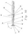
- FIG. 10is a side view of the display with several ray traces included.
- FIG. 11is a side view of the display with several ray traces included and the TIR light valves turned off.
- FIG. 12is a compressed broken section view of the light guide, LED, and light guide reflectors.
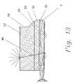
- FIG. 13is a side view of the flat panel display with all of the display components illustrated.
- FIG. 14is perspective view of a small section of the black mask.
- FIG. 15is a magnified side view of the TIR switch film component and the electronics back plane assembled together.
- FIG. 16is a schematic diagram of the control electronics required for color sequencing.
- FIG. 17illustrates the flat panel display utilizing a piezo or electroelastomer element.
- FIG. 18shows the flat panel display with a fixed reflector.
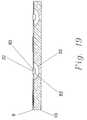
- FIG. 19shows the flat panel display with a hollow fixed reflector.
- the TIR switched thin flat panel display 1 of the present inventioncomprises a panel area 2 .
- the panel area 2has green LEDs 3 , blue LEDs 4 , and red LEDs 5 located along a lower edge.
- the number of LEDs 3 , 4 , 5 and the side where they are locatedis a function of the size, shape, and application of the desired display.
- the LEDs 3 , 4 , 5could be located on more than one edge should a specific application require it.
- the LEDs 3 , 4 , 5require driver electronics to drive them at the proper level and at the proper timing. A person skilled in the art of LED driver electronics could devise many different circuits to accomplish this task. In the embodiment illustrated in FIG.
- LEDs 3 , 4 , 5are shown generally equally spaced along the bottom edge. With the high efficiency inherent in the TIR technology, a display with this large number of LEDs would be intended for outdoor use, with high ambient light. A display intended for a use in low ambient light would require fewer LEDs 3 , 4 , 5 .
- FIG. 2is an exploded view of the panel area 2 , which comprises four major components.
- a mask and diffusion assembly 6forms a front layer of the panel area 2 .
- Behind the mask and diffusion assembly 6is a light guide 7 .
- Behind the light guide 7is a TIR switch film 8 .
- An electronics back plane 10is situated behind the TIR switch film 8 . All four of the major components 6 , 7 , 8 , 10 have the same area as a pixel area 11 . The number of pixels required is dependent on the display resolution.
- the four major components 6 , 7 , 8 , 10shown exploded in FIG. 2 , would in use be mated to one another as shown in FIG. 1 .
- a cross section of a small corner of the mated assemblyis shown enlarged in FIG. 3 .
- the green, blue, and red LEDs 3 , 4 , 5are shown in their true relationship to the light guide 7 .
- End reflector 9covers the same edge of the light guide 7 as do the LEDs 3 , 4 , 5 . (End reflector 9 is shown in greater detail in FIG. 12 , and its function will be discussed below.)
- the relative thicknesses of the major components 6 , 7 , 8 , 10can be seen in FIG. 12 .
- the relative thicknesses of the major components 6 , 7 , 8 , 10would change for different sizes and pitches of a given display.
- the substrate material for the electronics back plane 10should be an insulating material.
- a fiberglass reinforced PCB material or the likeis desirable as the substrate.
- the insulating substrate materialmay be glass, silicon, or plastic.
- the substrate materialdoes not need to be optically transparent, so there are many options for material selection.
- Electronic componentsmay be located on the planar surface 21 of the electronics back plane 10 .
- Annular rings 22are located near the centerline of the pixel areas.
- the annular rings 22are made of a conductive material, and are generally thin.
- the annular ring pocket 23is a recessed area for clearance from optical components (discussed below).
- the annular ring pockets 23are also made of conductive material and are thin. If any electronics were located on the backside of the electronics back plane 10 at least one feed through hole 24 would be required.
- the feed through holes 24are shown to be concentric to the annular ring 22 , but concentricity is not required.
- the feed through holes 24could be located anywhere on the electronics back plane 10 .
- the feed through holes 24have a thin layer of conductive material that connects the annular rings 22 to any electronics present on the backside of the electronics back plane 10 . It should be noted that any electronic components such as transistors, capacitors, or resistors that are required for the subject display application could be located either between the annular rings 22 or beneath the surface of the electronics back plane 10 .
- Bottom side annular rings 25are formed from a thin layer of conductive material to provide electrical conductivity with the feed through holes 24 .
- Conductive traces 26are used to connect the bottom side annular rings 25 to circuitry located elsewhere on the backside of the board.
- the bottom side annular rings 25can be connected to an electrical connector, which would put the bottom side annular rings 25 in communication with other electronic components on a remote PCB.
- One skilled in the art of electronic layout and manufacturingcould easily define the appropriate location and type of electronics to reduce the overall system cost while improving performance.
- the TIR switch film 8is shown in FIG. 6 .
- the TIR switch film 8is made of a transparent flexible type material such as polycarbonate, polyester, acrylic, or the like.
- the top surface 31 of the TIR switch film 8is situated in close proximity to the surface of the light guide 7 (not shown in FIG. 6 ), but there is a narrow gap between the top surface 31 of the TIR switch film 8 and the surface of the light guide 7 .
- the contact domes 32are ideally located in the center of the pixel area. (The contact domes 32 can be seen in more detail in FIG. 8 .)
- the contact domes 32preferably have a shallow taper and a flat region on a top surface. For very short contact domes 32 , the domes 32 may not have any taper at all.
- Each of the contact domes 32includes a reflector perimeter 33 .
- the reflector perimeter 33is positioned on the back side of the TIR switch film 8 , but is visible in FIG. 6 because the TIR switch film 8 is transparent.
- the TIR switch film 8is very thin to enable it to flex easily.
- the thickness of the TIR switch film 8is less than 1/10 the diameter of the reflector perimeter 33 .
- Spacer posts 34comprise another main element of the TIR switch film 8 .
- the spacer posts 34are located between the contact domes 32 .
- the spacer posts 34maintain the narrow gap 60 (visible in FIG. 15 ) between the TIR switch film 8 and the light guide 7 .
- the spacer posts 34are illustrated in FIGS. 6-8 as being square, but other shapes could be used as well.
- the spacer posts 34extend downward through the TIR switch film 8 and out the bottom side to form the bottom spacer posts 34 ′.
- the bottom spacer posts 34 ′can most easily be seen in FIG. 8 .
- FIG. 7shows the TIR switch film 8 assembled to the electronics back plane 10 .
- the annular rings 22 on the electronics back plane 10can be seen through the transparent TIR switch film 8 .
- the centerline of the pixel features of the TIR switch film 8 and the electronics back plane 10are generally in alignment.
- FIG. 8shows an exploded sectional side view of the electronics back plane 10 and the TIR switch film 8 .
- the annular ring pockets 23are shown in FIG. 8 as spherical in shape.
- the shape of the annular ring pockets 23could be rectangular, trapezoidal or an irregular shape.
- the shape of the annular ring pockets 23has no effect on the optical function of the invention.
- Reflectors 35are received in the annular ring pockets 23 .
- the shape of the reflector 35is depicted as generally spherical, a reflector shape that would be acceptable for many applications. However, in most display applications the ideal shape for the reflectors 35 would be aspheric.
- the specific optimal aspheric shape of the reflectors 35is a function of dome diameter, dome taper, dome position relative to the aspheric reflector, the index of refraction of the various components, and the diameter of the reflectors 35 . Additionally, manufacturing methods for the reflectors 35 may have a practical effect on the shape chosen for the reflectors 35 .
- One skilled in the art of the design of reflectorscould devise a reflector shape to meet the specific design goals of a given overall display.
- the bottom spacer posts 34 ′are formed from the lower end of the spacer posts 34 .
- the bottom surface of the bottom spacer posts 34 ′is in contact with and bonded to the planar surface 21 of the electronics back plane 10 .
- the top surface of the spacer post 34is bonded to the light guide 7 .
- the adhesive for this bondshould have a low index of refraction. If the adhesive has too high an index, the mating surface of the light guide 7 would need to be coated with a low index material.
- FIG. 9shows the TIR switch film 8 bonded to the light guide 7 .
- the contact domes 32are in contact with the light guide 7 . In those cases in which the light guide 7 is coated with a low index material, the areas where the contact domes 32 make contact with the light guide 7 must be void of the low index material.
- light rays 41originate from the green LED 3 .
- the light rays 41reflect off the film side surface 42 of the light guide 7 .
- This reflection of the light rays 41is total internal reflection, TIR.
- TIRoccurs when the angle from normal to the film side surface 42 to the direction of the ray, angle “A”, is less than the arcsine of the quotient of the index of refraction of the material adjacent to the surface of the light guide, “Ns”, to the index of refraction of the material of the light guide, “Nlg”.
- the internal angle Ais less than 41.8°, light reflects off of the internal surface. If the angle A is greater than 41.8°, the light passes through the surface and is refracted to a different angle.
- Case 1is when the light guide (index 1.5) is adjacent to air (index 1)
- Case 2is when the light guide (index 1.5) is adjacent a contact dome (index 1.5)
- Case 3is when the light guide (index 1.5) is adjacent a low index material (index 1.35)
- Case 1 and case 3are conditions where light would TIR. In case 2, the light does not TIR. The light passes through the surface of the light guide 7 and continues along its original path through the contact dome 32 .
- the light guide 7 and the contact dome 32may not have the same index of refraction. If the indexes of refraction are not equal, some refraction will take place at the interface of the light guide 7 and the contact dome 32 . The difference in the index of refraction between the materials determines the amount of the refraction. Preferably the index of refraction of the contact dome 32 is greater than that of the light guide 7 . If the index of refraction of the contact dome 32 is less than that of the light guide 7 , some of the light that is traveling at large angles normal to the surface of the light guide 7 would TIR and not pass through to the contact dome 32 .
- the reflection off the film side surface 42 using the air index of refractionis the first TIR reflection of light ray 41 .
- This reflectionwould be bound by the equation of case 1.
- the low index TIR reflection 44is a TIR reflection of the second light ray 43 , and is bound by the equation of case 3.
- the third internal light ray 45strikes the matched index point 46 and does not experience TIR.
- Third internal light rays 45pass through the light guide 7 and contact dome 32 materials without a reflection, assuming that when third internal light rays 45 impinge on this point, the contact dome 32 is in contact with the light guide 7 . It should be noted that the junction must be void of gaps. Even a small air gap would disrupt the passing of light.
- a small gapcan be created by a small variation in surface finish or even by a small foreign particle. Addition of a thin layer of transparent elastic material on either the surface of the light guide 7 or the surface of the contact domes 32 ensures that the disruptions will not occur and the light will pass as desired.
- the third internal light rays 45continue beyond the contact dome 32 and reflect off of the surface of the reflector 35 .
- the reflector 35is preferably coated with a high reflectance material such as aluminum, silver, or a dielectric coating.
- the contour of the reflector 35 surfacedetermines the direction of the reflected light 48 .
- the contoured reflectors 35are preferably aspheric in shape.
- FIG. 11shows the same elements as are shown in FIG. 10 , but in FIG. 1 the contact dome 32 is not in contact with the light guide 7 .
- the index of refraction at the surface of the light guide 7is that of air.
- case 1light TIRs off the surface of the light guide 7 .
- Light rays 49continue to TIR along the inside of the light guide 7 until the rays 49 impinge on a contact dome 32 that is in contact with the light guide 7 .
- a contact dome 32 associated with a particular pixelis in contact with the surface of the light guide 7 , that pixel is in an on state.
- the contact dome 32is not in contact with the light guide 7 , the pixel is off.
- FIG. 12shows the light guide 7 , LED 3 , and the end reflectors 9 and 9 ′ in side magnified view.
- End reflectors 9 , 9 ′are preferably formed from a material that has a high reflectance.
- End reflectors 9 , 9 ′can be interference type or metal reflectors, or the reflectors 9 , 9 ′ could be angled retro type reflectors.
- Lightwill often travel the length of the light guide 7 from the LED 3 and not strike a contact dome 32 that is in the on position.
- the lightwill therefore TIR and will not be extracted from the light guide 7 .
- the lightcontinues to travel along the full length of the light guide 7 until the light reaches the distal end of the light guide 7 , and is reflected off end reflector 9 ′. This reflection redirects the light in the opposite direction back through the light guide 7 .
- the lightthen travels back along the length of the light guide 7 , and assuming it strikes no activated contact domes 32 , will return to the first end of the light guide 7 , the end on which the LEDs 3 , 4 , 5 are located.
- the lightwill either strike the area between the LEDs 3 , 4 , 5 or it will strike the LEDs 3 , 4 , 5 .
- the lightwill be reflected by the end reflector 9 .
- the TIR switched thin flat panel display 1has only a few LEDs 3 , 4 , 5 , the light will almost always reflect off of the high reflectance end reflector 9 . In some cases the light will reflect off of an LED 3 , 4 , 5 .
- the LED 3 , 4 , 5will absorb a portion of the light, and the remainder of the light will be reflected. Light may travel up and down the light guide 7 a number of times before it is extracted by a contact dome 32 .
- the end reflectors 9 , 9 ′may have reflectance efficiencies of 98% or better, and good quality light guide material absorbs very little light.
- the mask and diffusion assembly 6is mounted above the panel area 2 .
- the mask and diffusion assembly 6is a multi-layered assembly, comprising a low index layer 51 , a spacer plate 52 , a mask plate 53 , a first diffuser 55 , a second spacer 56 , and a second diffuser 57 .
- the low index layer 51is thin and has a low index of refraction.
- An air gap or a vacuum layercould serve as the low index layer 51 , but forming the low index layer 51 from a low refraction index solid material is often beneficial to the assembly of the device.
- the low index layer 51will typically be an adhesive that affixes the spacer plate 52 to the light guide 7 .
- the low index layer 51 and the spacer plate 52can be combined into one element, a thicker low index layer 51 .
- the use of two different materials to form the low index layer 51 and the spacer plate 52is more beneficial.
- the mask plate 53contains multiple aperture holes 54 (see FIG. 15 ) to allow the reflected light 48 to pass through the mask plate 53 .
- the remaining area of the mask plate 53is preferably high absorbing black material. Black chrome, carbon black, or an organic material are three types of material that would serve as suitable materials for the mask plate 53 .
- the mask plate 53increases the contrast ratio of the display when ambient light is present.
- the mask plate 53absorbs light that would otherwise reflect from the TIR switch film 8 or any of its components. For inexpensive displays, where cost is more important than quality, the mask plate 53 can be eliminated. Also, the mask plate 53 may be eliminated where the display is only used in low ambient lighting conditions. An example of a low ambient light environment would be a motion picture cinema.
- the first diffuser 55is an optional diffuser to spread the light coming from the reflectors 35 .
- the first diffuser 55may not be required, but for displays with large pixels, the first diffuser 55 should be included. It should also be noted that the positions of the mask plate 53 and the first diffuser 55 could be reversed without affecting the function of the display.
- the second spacer 56allows the light transmitted from the reflectors 35 to begin to spread out.
- the second diffuser 57is used to spread the light still further so that the viewer can be at a position far from normal to the display and still see the light from the reflectors 35 .
- the amount and direction of diffusion that is incorporated into the second diffuser 57will vary for different types of displays. For example, small cell phone displays typically have a smaller viewing angle in both the vertical and horizontal directions. TVs typically have a large viewing angle in the horizontal direction and not as big a viewing angle in the vertical direction.
- the TIR switch film 8is assembled to the electronics back plane 10 .
- the annular rings 22 of the electronics back plane 10are in close proximity to the bottom surface of the TIR switch film 8 .
- the bottom surface of the TIR switch film 8is coated with a conductive layer 62 .
- the conductive layer 62may be a continuation of the surface of the reflector 35 .
- the contact domes 32can be driven against or removed from contact with the surface of the light guide 7 (not shown in FIG. 15 ).
- either one or both of the charged surfacesis coated with an insulating layer.
- electrostatic forceis not the only means that can be used to control the contact of the contact domes 32 with the surface of the light guide 7 .
- One alternate methodwould be the use of a piezoelectric material.
- actuation devicescould devise many ways to change the positions of the contact domes 32 .
- electronic circuitsthat could be devised to drive the actuator.
- FIG. 16depicts schematic representations of the circuitry used to create colors at the pixels.
- the switch for pixel n,mis moved to a state that has the contact dome 32 in contact with the light guide 7 , and the driver for the green LED 3 is turned on.
- the blue and red LEDs 4 , 5would not be on. (One exception to this case is if the display was only creating a black and white image. Then all three LEDs 3 , 4 , 5 would be on at the same time.
- the contact dome 32 associated with pixel n,mremains in contact with the light guide 7 for the appropriate period of time to allow the desired amount of light to exit the pixel to create to create the desired intensity for the viewer.
- the contact dome 32is placed in contact with the light guide 7 when the blue LED 4 is on.
- the contact dome 32remains in contact the amount of time required to create the particular intensity needed for the viewer. Red colors are created in a similar manner.
- the contact dome 32is placed in contact with the light guide for two or more periods when two or three of the LEDs 3 , 4 , 5 are on.
- the contact dome 32would extract light from the light guide 7 when the red LED 5 is on. After the red LED 5 goes off, the blue LED 4 is turned on. The contact dome 32 does not extract light during the time the blue LED 4 is on. The green LED 3 would be turned on after the blue LED 4 is turned off. When the green LED 3 is on, the contact dome 32 would again allow light to reach the viewer. This would happen hundreds of times per second resulting in the human eye integrating the red and green into yellow. The length of time that the contact dome 32 allows light to reach the viewer determines the brightness. By altering the individual time periods for the red and green the hue of the yellow can be controlled. Some blue light can be added to reduce the saturation of the yellow.
- LEDsdo not typically emit a wide range of wavelengths of light.
- a high quality displaymay include LEDs with wavelengths between the primary RGB LEDs. Examples are orange, cyan and yellow. By adding these extra wavelengths the spectrum output of the TIR display could be made to match what a viewer would see in the real world. Very little additional circuitry is required to add this improved performance.
- electronicsare required to control the switches and the LEDs of the present invention. Electronics are also required to relate the operation of the optics elements to a computer, TV, or other type of video signal. Control electronics of this type are created for display systems that create colors by multiplexing the colors in time. One skilled in the art would be able to devise many ways to accomplish this task.
- the innovative part of this inventionis the optical switching and optics, not the configuration of the electronic components.
- FIG. 17illustrates the device using a piezoelectric material 70 as the actuating mechanism.
- This embodimentshows the piezoelectric material 70 attached to the reflector surface 35 .
- the piezoelectric material 70is driven with the same type electronics back plane 10 as is used to drive the electrostatic force switching mechanism. By changing the height of the piezoelectric material 70 , the surface of the reflector 35 , and therefore the contact dome 32 , can be turned on and off.
- FIG. 18shows the contact domes 32 mounted on angled cones 80 on the TIR switch film 8 .
- This configurationis preferred when the reflector size is large.
- the reflector 35would be stationary and would have an angled cone relieved area 82 slightly larger than the angled cone 80 mounted on the TIR switch film 8 .
- the angled cone relieved area 82allows clearance for the contact dome 32 and the angled cone 80 to move into contact with, and away from, the light guide 7 .
- FIG. 19illustrates a configuration of the device in which the reflector area 35 ′ is void of material and would be air or a vacuum. The reflector area 35 ′ would still be employed to reflect light.
Landscapes
- Physics & Mathematics (AREA)
- General Physics & Mathematics (AREA)
- Optics & Photonics (AREA)
- Engineering & Computer Science (AREA)
- Theoretical Computer Science (AREA)
- Devices For Indicating Variable Information By Combining Individual Elements (AREA)
- Planar Illumination Modules (AREA)
Abstract
Description
AngleA=arcsine(1/1.5)=41.8° forNs=1 andNlg=1.5
A=arcsine(Ns/Nlg)
Claims (24)
Priority Applications (13)
| Application Number | Priority Date | Filing Date | Title |
|---|---|---|---|
| US12/319,171US8272770B2 (en) | 2009-01-02 | 2009-01-02 | TIR switched flat panel display |
| US13/143,342US8651724B2 (en) | 2009-01-02 | 2009-12-31 | TIR switched flat panel display |
| PCT/US2009/006763WO2010077367A2 (en) | 2009-01-02 | 2009-12-31 | Optic system for light guide with controlled output |
| EP09809010AEP2384455A2 (en) | 2009-01-02 | 2009-12-31 | Light guide system for extracting light with controlled output |
| JP2011544420AJP2012514835A (en) | 2009-01-02 | 2009-12-31 | Optical system for light guide with control output |
| JP2011544418AJP2012514761A (en) | 2009-01-02 | 2009-12-31 | Total reflection to switch flat panel display |
| KR1020117018090AKR20110139194A (en) | 2009-01-02 | 2009-12-31 | Total internal reflection switchable flat panel display |
| EP09799444AEP2384454A1 (en) | 2009-01-02 | 2009-12-31 | Total internal reflection switched flat panel display |
| PCT/US2009/006757WO2010077363A1 (en) | 2009-01-02 | 2009-12-31 | Total internal reflection switched flat panel display |
| US13/143,341US8641257B2 (en) | 2009-01-02 | 2009-12-31 | Optic system for light guide with controlled output |
| CN2009801562709ACN102341748A (en) | 2009-01-02 | 2009-12-31 | Light guide system with controlled output for light extraction |
| CN2009801562728ACN102395922A (en) | 2009-01-02 | 2009-12-31 | Total Internal Reflection Switching Flat Panel Display |
| KR1020117018088AKR20110139193A (en) | 2009-01-02 | 2009-12-31 | Light guide system extracts light at a controlled output |
Applications Claiming Priority (1)
| Application Number | Priority Date | Filing Date | Title |
|---|---|---|---|
| US12/319,171US8272770B2 (en) | 2009-01-02 | 2009-01-02 | TIR switched flat panel display |
Related Parent Applications (2)
| Application Number | Title | Priority Date | Filing Date |
|---|---|---|---|
| US12/319,172ContinuationUS8152352B2 (en) | 2009-01-02 | 2009-01-02 | Optic system for light guide with controlled output |
| US12/319,172Continuation-In-PartUS8152352B2 (en) | 2009-01-02 | 2009-01-02 | Optic system for light guide with controlled output |
Related Child Applications (4)
| Application Number | Title | Priority Date | Filing Date |
|---|---|---|---|
| US12/319,172ContinuationUS8152352B2 (en) | 2009-01-02 | 2009-01-02 | Optic system for light guide with controlled output |
| US13/143,341ContinuationUS8641257B2 (en) | 2009-01-02 | 2009-12-31 | Optic system for light guide with controlled output |
| US13/143,341Continuation-In-PartUS8641257B2 (en) | 2009-01-02 | 2009-12-31 | Optic system for light guide with controlled output |
| US13/143,342Continuation-In-PartUS8651724B2 (en) | 2009-01-02 | 2009-12-31 | TIR switched flat panel display |
Publications (2)
| Publication Number | Publication Date |
|---|---|
| US20100172138A1 US20100172138A1 (en) | 2010-07-08 |
| US8272770B2true US8272770B2 (en) | 2012-09-25 |
Family
ID=42311581
Family Applications (2)
| Application Number | Title | Priority Date | Filing Date |
|---|---|---|---|
| US12/319,171Expired - Fee RelatedUS8272770B2 (en) | 2009-01-02 | 2009-01-02 | TIR switched flat panel display |
| US13/143,341Expired - Fee RelatedUS8641257B2 (en) | 2009-01-02 | 2009-12-31 | Optic system for light guide with controlled output |
Family Applications After (1)
| Application Number | Title | Priority Date | Filing Date |
|---|---|---|---|
| US13/143,341Expired - Fee RelatedUS8641257B2 (en) | 2009-01-02 | 2009-12-31 | Optic system for light guide with controlled output |
Country Status (1)
| Country | Link |
|---|---|
| US (2) | US8272770B2 (en) |
Cited By (22)
| Publication number | Priority date | Publication date | Assignee | Title |
|---|---|---|---|---|
| US20110149595A1 (en)* | 2009-12-23 | 2011-06-23 | Global Lighting Technology Inc. | Light guide plate, backlight module and method of guiding light |
| US20110267838A1 (en)* | 2009-01-02 | 2011-11-03 | Richardson Brian E | Optic System for Light Guide with Controlled Output |
| US8651724B2 (en) | 2009-01-02 | 2014-02-18 | Rambus Delaware Llc | TIR switched flat panel display |
| US20140355302A1 (en)* | 2013-03-15 | 2014-12-04 | Cree, Inc. | Outdoor and/or Enclosed Structure LED Luminaire for General Illumination Applications, Such as Parking Lots and Structures |
| US9291320B2 (en) | 2013-01-30 | 2016-03-22 | Cree, Inc. | Consolidated troffer |
| US9366799B2 (en) | 2013-03-15 | 2016-06-14 | Cree, Inc. | Optical waveguide bodies and luminaires utilizing same |
| US9366396B2 (en) | 2013-01-30 | 2016-06-14 | Cree, Inc. | Optical waveguide and lamp including same |
| US9389367B2 (en) | 2013-01-30 | 2016-07-12 | Cree, Inc. | Optical waveguide and luminaire incorporating same |
| US9411086B2 (en) | 2013-01-30 | 2016-08-09 | Cree, Inc. | Optical waveguide assembly and light engine including same |
| US9442243B2 (en) | 2013-01-30 | 2016-09-13 | Cree, Inc. | Waveguide bodies including redirection features and methods of producing same |
| US9625638B2 (en) | 2013-03-15 | 2017-04-18 | Cree, Inc. | Optical waveguide body |
| US9690029B2 (en) | 2013-01-30 | 2017-06-27 | Cree, Inc. | Optical waveguides and luminaires incorporating same |
| US9798072B2 (en) | 2013-03-15 | 2017-10-24 | Cree, Inc. | Optical element and method of forming an optical element |
| US9869432B2 (en) | 2013-01-30 | 2018-01-16 | Cree, Inc. | Luminaires using waveguide bodies and optical elements |
| US9920901B2 (en) | 2013-03-15 | 2018-03-20 | Cree, Inc. | LED lensing arrangement |
| US10209429B2 (en) | 2013-03-15 | 2019-02-19 | Cree, Inc. | Luminaire with selectable luminous intensity pattern |
| US10234616B2 (en) | 2013-01-30 | 2019-03-19 | Cree, Inc. | Simplified low profile module with light guide for pendant, surface mount, wall mount and stand alone luminaires |
| US10416377B2 (en) | 2016-05-06 | 2019-09-17 | Cree, Inc. | Luminaire with controllable light emission |
| US10436970B2 (en) | 2013-03-15 | 2019-10-08 | Ideal Industries Lighting Llc | Shaped optical waveguide bodies |
| US10502899B2 (en)* | 2013-03-15 | 2019-12-10 | Ideal Industries Lighting Llc | Outdoor and/or enclosed structure LED luminaire |
| US11112083B2 (en) | 2013-03-15 | 2021-09-07 | Ideal Industries Lighting Llc | Optic member for an LED light fixture |
| US11719882B2 (en) | 2016-05-06 | 2023-08-08 | Ideal Industries Lighting Llc | Waveguide-based light sources with dynamic beam shaping |
Families Citing this family (29)
| Publication number | Priority date | Publication date | Assignee | Title |
|---|---|---|---|---|
| US7499206B1 (en)* | 2005-12-09 | 2009-03-03 | Brian Edward Richardson | TIR light valve |
| US20100214282A1 (en) | 2009-02-24 | 2010-08-26 | Dolby Laboratories Licensing Corporation | Apparatus for providing light source modulation in dual modulator displays |
| US8297818B2 (en) | 2009-06-11 | 2012-10-30 | Rambus International Ltd. | Optical system with reflectors and light pipes |
| US20100315836A1 (en)* | 2009-06-11 | 2010-12-16 | Brian Edward Richardson | Flat panel optical display system with highly controlled output |
| US8152318B2 (en)* | 2009-06-11 | 2012-04-10 | Rambus International Ltd. | Optical system for a light emitting diode with collection, conduction, phosphor directing, and output means |
| US8339028B2 (en)* | 2009-06-30 | 2012-12-25 | Apple Inc. | Multicolor light emitting diodes |
| KR20120095437A (en)* | 2009-11-18 | 2012-08-28 | 램버스 인터내셔널 리미티드 | Internal Acquisition Reflective Optics Using Light Emitting Diodes |
| TW201213970A (en)* | 2010-09-30 | 2012-04-01 | Global Lighting Technolog Inc | Backlight module and liquid crystal display |
| WO2012082825A2 (en) | 2010-12-17 | 2012-06-21 | Dolby Laboratories Licensing Corporation | Quantum dots for display panels |
| TW201300702A (en) | 2011-05-13 | 2013-01-01 | Rambus Inc | Lighting assembly |
| US20120320627A1 (en)* | 2011-05-17 | 2012-12-20 | Pixi Lighting Llc | Flat panel lighting device and driving circuitry |
| KR102118309B1 (en) | 2012-09-19 | 2020-06-03 | 돌비 레버러토리즈 라이쎈싱 코오포레이션 | Quantum dot/remote phosphor display system improvements |
| BR122017001987B1 (en) | 2013-03-08 | 2022-04-05 | Dolby Laboratories Licensing Corporation | Visualization system and apparatus for monitor techniques with dual modulation with light conversion |
| US9500328B2 (en) | 2013-04-17 | 2016-11-22 | Pixi Lighting, Inc. | Lighting assembly |
| US9546781B2 (en) | 2013-04-17 | 2017-01-17 | Ever Venture Solutions, Inc. | Field-serviceable flat panel lighting device |
| US9476552B2 (en) | 2013-04-17 | 2016-10-25 | Pixi Lighting, Inc. | LED light fixture and assembly method therefor |
| US10262462B2 (en) | 2014-04-18 | 2019-04-16 | Magic Leap, Inc. | Systems and methods for augmented and virtual reality |
| US20160131804A1 (en)* | 2013-07-22 | 2016-05-12 | Motorola Solutions, Inc. | Display system for a communication device |
| US9291340B2 (en) | 2013-10-23 | 2016-03-22 | Rambus Delaware Llc | Lighting assembly having n-fold rotational symmetry |
| CN111243533B (en) | 2014-03-26 | 2022-11-25 | 杜比实验室特许公司 | Global light compensation in various displays |
| EP3633663B1 (en) | 2014-08-21 | 2024-06-19 | Dolby Laboratories Licensing Corporation | Techniques for dual modulation with light conversion |
| US9557022B2 (en) | 2015-04-30 | 2017-01-31 | Ever Venture Solutions, Inc. | Non-round retrofit recessed LED lighting fixture |
| WO2017042699A1 (en) | 2015-09-07 | 2017-03-16 | Sabic Global Technologies B.V. | Molding of plastic glazing of tailgates |
| EP3347183B1 (en) | 2015-09-07 | 2020-12-16 | SABIC Global Technologies B.V. | Plastic glazing for a tailgate of a vehicle having a light assembly |
| US10434846B2 (en) | 2015-09-07 | 2019-10-08 | Sabic Global Technologies B.V. | Surfaces of plastic glazing of tailgates |
| US10597097B2 (en) | 2015-09-07 | 2020-03-24 | Sabic Global Technologies B.V. | Aerodynamic features of plastic glazing of tailgates |
| CN105158831B (en)* | 2015-10-23 | 2018-11-30 | 深圳市华星光电技术有限公司 | A kind of flexible board |
| KR102140566B1 (en) | 2015-11-23 | 2020-08-04 | 사빅 글로벌 테크놀러지스 비.브이. | Lighting system for windows having plastic glazing |
| US11280957B1 (en)* | 2020-11-05 | 2022-03-22 | TieJun Wang | Glass light guide plate |
Citations (86)
| Publication number | Priority date | Publication date | Assignee | Title |
|---|---|---|---|---|
| US223898A (en) | 1879-11-04 | 1880-01-27 | Thomas Alva Edison | Electric lamp |
| GB663840A (en) | 1946-12-18 | 1951-12-27 | Edgar Gretener | A regulable optical illumination system |
| US2673923A (en) | 1947-12-03 | 1954-03-30 | Duro Test Corp | Means for producing colored light beams |
| US2971083A (en) | 1958-11-14 | 1961-02-07 | Gen Electric | Low brightness louver |
| US4172631A (en) | 1975-01-07 | 1979-10-30 | Izon Corporation | Parallel optical fiber and strip illuminating arrays |
| US4392187A (en) | 1981-03-02 | 1983-07-05 | Vari-Lite, Ltd. | Computer controlled lighting system having automatically variable position, color, intensity and beam divergence |
| US4566935A (en) | 1984-07-31 | 1986-01-28 | Texas Instruments Incorporated | Spatial light modulator and method |
| US4596992A (en) | 1984-08-31 | 1986-06-24 | Texas Instruments Incorporated | Linear spatial light modulator and printer |
| US4615595A (en) | 1984-10-10 | 1986-10-07 | Texas Instruments Incorporated | Frame addressed spatial light modulator |
| US4662746A (en) | 1985-10-30 | 1987-05-05 | Texas Instruments Incorporated | Spatial light modulator and method |
| US4710732A (en) | 1984-07-31 | 1987-12-01 | Texas Instruments Incorporated | Spatial light modulator and method |
| US4956619A (en) | 1988-02-19 | 1990-09-11 | Texas Instruments Incorporated | Spatial light modulator |
| US4972306A (en) | 1989-01-23 | 1990-11-20 | Vari-Lite, Inc. | Compact variable diffuser for use in a luminaire |
| US5028939A (en) | 1988-08-23 | 1991-07-02 | Texas Instruments Incorporated | Spatial light modulator system |
| US5083252A (en) | 1990-04-19 | 1992-01-21 | Tailored Lighting Company, Inc. | Apparatus for producing light distributions |
| US5126886A (en) | 1989-04-10 | 1992-06-30 | Morpheus Lights, Inc. | Scrolling primary color changer |
| US5217285A (en) | 1991-03-15 | 1993-06-08 | The United States Of America As Represented By United States Department Of Energy | Apparatus for synthesis of a solar spectrum |
| US5221987A (en) | 1992-04-10 | 1993-06-22 | Laughlin Richard H | FTIR modulator |
| US5319491A (en) | 1990-08-10 | 1994-06-07 | Continental Typographics, Inc. | Optical display |
| US5396350A (en) | 1993-11-05 | 1995-03-07 | Alliedsignal Inc. | Backlighting apparatus employing an array of microprisms |
| US5467208A (en) | 1992-06-01 | 1995-11-14 | Sharp Kabushiki Kaisha | Liquid crystal display |
| US5631895A (en) | 1994-10-18 | 1997-05-20 | Nec Corporation | Optical information recording medium |
| EP0814300A1 (en) | 1996-06-21 | 1997-12-29 | Casio Computer Company Limited | Surface light source device and liquid crystal display device using the same |
| EP0867747A2 (en) | 1997-03-25 | 1998-09-30 | Sony Corporation | Reflective display device |
| US5825548A (en) | 1997-09-11 | 1998-10-20 | Vari-Lite, Inc. | Cross-fading color filter and system |
| US5936772A (en) | 1997-04-16 | 1999-08-10 | Oympus Optical Co., Ltd. | Light source optical system for endoscopes |
| US5953469A (en) | 1996-10-29 | 1999-09-14 | Xeotron Corporation | Optical device utilizing optical waveguides and mechanical light-switches |
| US5995690A (en) | 1996-11-21 | 1999-11-30 | Minnesota Mining And Manufacturing Company | Front light extraction film for light guiding systems and method of manufacture |
| EP0969306A1 (en) | 1998-01-20 | 2000-01-05 | Seiko Epson Corporation | Optical switching device and image display device |
| EP0969305A1 (en) | 1998-01-20 | 2000-01-05 | Seiko Epson Corporation | Optical switching device, image display and projection device |
| US6040937A (en) | 1994-05-05 | 2000-03-21 | Etalon, Inc. | Interferometric modulation |
| US6048081A (en) | 1998-06-15 | 2000-04-11 | Richardson; Brian Edward | Beam divergence and shape controlling module for projected light |
| US6350041B1 (en) | 1999-12-03 | 2002-02-26 | Cree Lighting Company | High output radial dispersing lamp using a solid state light source |
| US6360033B1 (en) | 1999-11-25 | 2002-03-19 | Electronics And Telecommunications Research Institute | Optical switch incorporating therein shallow arch leaf springs |
| US20020044720A1 (en) | 2000-10-17 | 2002-04-18 | Brophy Christopher P. | System for aligning connectors and optical devices |
| EP1215526A1 (en) | 2000-07-11 | 2002-06-19 | Mitsubishi Chemical Corporation | Surface light source device |
| US6421103B2 (en) | 1999-12-28 | 2002-07-16 | Fuji Photo Film Co., Ltd. | Liquid-crystal display apparatus including a backlight section using collimating plate |
| US6421104B1 (en) | 1999-10-22 | 2002-07-16 | Motorola, Inc. | Front illuminator for a liquid crystal display and method of making same |
| US20020105709A1 (en) | 1997-09-04 | 2002-08-08 | Whitehead Lorne A. | Optical switching by controllable frustration of total internal reflection |
| JP2002229017A (en) | 2001-02-07 | 2002-08-14 | Sharp Corp | Display device |
| US6438283B1 (en) | 1999-10-08 | 2002-08-20 | Optical Switch Corporation | Frustrated total internal reflection switch using double pass reflection and method of operation |
| US6502961B1 (en) | 2000-11-20 | 2003-01-07 | Brian Edward Richardson | Conical lens array to control projected light beam color, divergence, and shape |
| EP1291833A2 (en) | 2001-09-06 | 2003-03-12 | Ngk Insulators, Ltd. | Display system with cooling device |
| US6565233B1 (en) | 1999-08-17 | 2003-05-20 | Brian Edward Richardson | Color, size and distribution module for projected light |
| US6674562B1 (en) | 1994-05-05 | 2004-01-06 | Iridigm Display Corporation | Interferometric modulation of radiation |
| US20040076396A1 (en) | 2001-02-14 | 2004-04-22 | Yoshinori Suga | Light guiding body, light reflective sheet, surface light source device and liquid crystal display device using the light reflective sheet, and method of manufacturing the light reflective sheet |
| US6729734B2 (en) | 2002-04-01 | 2004-05-04 | Hewlett-Packard Development Company, L.P. | System for enhancing the quality of an image |
| US20040109105A1 (en) | 2002-11-29 | 2004-06-10 | Alps Electric Co., Ltd. | Backlight unit and liquid crystal display device |
| US6768572B2 (en) | 1997-10-29 | 2004-07-27 | Teloptics Corporation | Solid state free space switch array on a substrate |
| US6771325B1 (en) | 1999-11-05 | 2004-08-03 | Texas Instruments Incorporated | Color recapture for display systems |
| WO2004068183A2 (en) | 2003-01-27 | 2004-08-12 | 3M Innovative Properties Company | Phosphor based light sources having an polymeric long pass reflector |
| US6824270B2 (en) | 2002-08-29 | 2004-11-30 | Samsung Electronics Co., Ltd. | Single-panel color image display apparatus and scrolling method |
| US20050018147A1 (en) | 2003-06-10 | 2005-01-27 | Samsung Electronics Co., Ltd. | Compact LED module and projection display adopting the same |
| US20050057731A1 (en) | 2003-09-17 | 2005-03-17 | Young-Chol Lee | Projection display |
| US6924945B1 (en) | 2003-10-28 | 2005-08-02 | Brian Edward Richardson | Compact light collection system with improved efficiency and reduced size |
| US20050221473A1 (en) | 2004-03-30 | 2005-10-06 | Intel Corporation | Sensor array integrated circuits |
| US20050243570A1 (en) | 2004-04-23 | 2005-11-03 | Chaves Julio C | Optical manifold for light-emitting diodes |
| US20050248827A1 (en) | 2002-03-01 | 2005-11-10 | Starkweather Gary K | Reflective microelectrical mechanical structure (MEMS) optical modulator and optical display system |
| US20050270796A1 (en) | 2004-06-07 | 2005-12-08 | Mitsubishi Denki Kabushiki Kaisha | Planar light source device and display device using the same |
| US6974232B1 (en) | 2003-10-14 | 2005-12-13 | Brian Edward Richardson | Compact lighting system with improved light transmission and color filters |
| US20060070379A1 (en) | 2000-10-31 | 2006-04-06 | Microsoft Corporation | Microelectrical mechanical structure (MEMS) optical modulator and optical display system |
| US7080932B2 (en) | 2004-01-26 | 2006-07-25 | Philips Lumileds Lighting Company, Llc | LED with an optical system to increase luminance by recycling emitted light |
| US7123216B1 (en) | 1994-05-05 | 2006-10-17 | Idc, Llc | Photonic MEMS and structures |
| US7142744B2 (en) | 2001-05-14 | 2006-11-28 | Calient Networks | Wavelength power equalization by attenuation in an optical switch |
| US7144131B2 (en) | 2004-09-29 | 2006-12-05 | Advanced Optical Technologies, Llc | Optical system using LED coupled with phosphor-doped reflective materials |
| US7177498B2 (en) | 2002-03-13 | 2007-02-13 | Altera Corporation | Two-by-two optical routing element using two-position MEMS mirrors |
| US20070133224A1 (en) | 1995-06-27 | 2007-06-14 | Parker Jeffery R | Light emitting panel assemblies |
| US20070176887A1 (en) | 2006-01-31 | 2007-08-02 | Uehara Shin-Ichi | Display device, terminal device, and display panel |
| US20070211487A1 (en) | 2004-09-20 | 2007-09-13 | Koninklijke Philips Electronics, N.V. | Led collimator element with a semiparabolic reflector |
| US7345824B2 (en) | 2002-03-26 | 2008-03-18 | Trivium Technologies, Inc. | Light collimating device |
| WO2008060335A1 (en) | 2006-11-17 | 2008-05-22 | Rensselaer Polytechnic Institute | High-power white leds and manufacturing method thereof |
| US7380962B2 (en) | 2004-04-23 | 2008-06-03 | Light Prescriptions Innovators, Llc | Optical manifold for light-emitting diodes |
| US20080247169A1 (en) | 2004-03-16 | 2008-10-09 | Koninklijke Philips Electronics, N.V. | High Brightness Illumination Device With Incoherent Solid State Light Source |
| US7447397B1 (en) | 2004-06-14 | 2008-11-04 | Dynamic Method Enterprises Limited | Optical switch matrix |
| WO2009024952A2 (en) | 2007-08-23 | 2009-02-26 | Koninklijke Philips Electronics N.V. | Light source including reflective wavelength-converting layer |
| US7499206B1 (en) | 2005-12-09 | 2009-03-03 | Brian Edward Richardson | TIR light valve |
| US20090064993A1 (en) | 2007-09-10 | 2009-03-12 | Banyan Energy, Inc. | Solar energy concentrator |
| EP2045633A1 (en) | 2007-10-04 | 2009-04-08 | Samsung Electronics Co., Ltd. | All-in-one type light guide plate with protrusions of inverted truncated prisms and backlight apparatus employing the same |
| US20090262368A1 (en) | 2008-04-18 | 2009-10-22 | Avago Technologies Ecbu Ip (Singapore) Pte. Ltd. | Light pipe for low profile optical navigation systems |
| US20100085773A1 (en) | 2009-01-02 | 2010-04-08 | Brian Edward Richardson | Optic system light guide with controlled output |
| US20100135040A1 (en)* | 2002-12-12 | 2010-06-03 | Hitachi Displays, Ltd. | Light-Emitting Element and Display Device Using Same |
| US20100172138A1 (en) | 2009-01-02 | 2010-07-08 | Brian Edward Richardson | Tir switched flat panel display |
| US20100220492A1 (en) | 2009-06-11 | 2010-09-02 | Brian Edward Richardson | Optical system with reflectors and light pipes |
| US20100315836A1 (en) | 2009-06-11 | 2010-12-16 | Brian Edward Richardson | Flat panel optical display system with highly controlled output |
| US20100315802A1 (en) | 2009-06-11 | 2010-12-16 | Brian Edward Richardson | Optical system for a Light Emitting Diode with collection, conduction, phosphor directing, and output means |
| US8025434B2 (en)* | 2008-06-03 | 2011-09-27 | Nokia Corporation | Two-sided illumination device |
Family Cites Families (5)
| Publication number | Priority date | Publication date | Assignee | Title |
|---|---|---|---|---|
| JP4404174B2 (en) | 2000-04-19 | 2010-01-27 | ソニー株式会社 | Optical switching element, switching device using the same, and image display device |
| US6595652B2 (en)* | 2000-12-12 | 2003-07-22 | International Manufacturing And Engineering Services Co., Ltd. | Surface lighting device |
| US6864620B2 (en) | 2000-12-22 | 2005-03-08 | Ngk Insulators, Ltd. | Matrix type actuator |
| KR20050109579A (en) | 2003-03-18 | 2005-11-21 | 코닌클리케 필립스 일렉트로닉스 엔.브이. | Foil display with increased brightness using a retro reflector |
| JP2005249882A (en) | 2004-03-01 | 2005-09-15 | Miyakawa:Kk | Liquid crystal display device |
- 2009
- 2009-01-02USUS12/319,171patent/US8272770B2/ennot_activeExpired - Fee Related
- 2009-12-31USUS13/143,341patent/US8641257B2/ennot_activeExpired - Fee Related
Patent Citations (93)
| Publication number | Priority date | Publication date | Assignee | Title |
|---|---|---|---|---|
| US223898A (en) | 1879-11-04 | 1880-01-27 | Thomas Alva Edison | Electric lamp |
| GB663840A (en) | 1946-12-18 | 1951-12-27 | Edgar Gretener | A regulable optical illumination system |
| US2673923A (en) | 1947-12-03 | 1954-03-30 | Duro Test Corp | Means for producing colored light beams |
| US2971083A (en) | 1958-11-14 | 1961-02-07 | Gen Electric | Low brightness louver |
| US4172631A (en) | 1975-01-07 | 1979-10-30 | Izon Corporation | Parallel optical fiber and strip illuminating arrays |
| US4392187A (en) | 1981-03-02 | 1983-07-05 | Vari-Lite, Ltd. | Computer controlled lighting system having automatically variable position, color, intensity and beam divergence |
| US4566935A (en) | 1984-07-31 | 1986-01-28 | Texas Instruments Incorporated | Spatial light modulator and method |
| US4710732A (en) | 1984-07-31 | 1987-12-01 | Texas Instruments Incorporated | Spatial light modulator and method |
| US4596992A (en) | 1984-08-31 | 1986-06-24 | Texas Instruments Incorporated | Linear spatial light modulator and printer |
| US4615595A (en) | 1984-10-10 | 1986-10-07 | Texas Instruments Incorporated | Frame addressed spatial light modulator |
| US4662746A (en) | 1985-10-30 | 1987-05-05 | Texas Instruments Incorporated | Spatial light modulator and method |
| US4956619A (en) | 1988-02-19 | 1990-09-11 | Texas Instruments Incorporated | Spatial light modulator |
| US5028939A (en) | 1988-08-23 | 1991-07-02 | Texas Instruments Incorporated | Spatial light modulator system |
| US4972306A (en) | 1989-01-23 | 1990-11-20 | Vari-Lite, Inc. | Compact variable diffuser for use in a luminaire |
| US5126886A (en) | 1989-04-10 | 1992-06-30 | Morpheus Lights, Inc. | Scrolling primary color changer |
| US5083252A (en) | 1990-04-19 | 1992-01-21 | Tailored Lighting Company, Inc. | Apparatus for producing light distributions |
| US5319491A (en) | 1990-08-10 | 1994-06-07 | Continental Typographics, Inc. | Optical display |
| US5217285A (en) | 1991-03-15 | 1993-06-08 | The United States Of America As Represented By United States Department Of Energy | Apparatus for synthesis of a solar spectrum |
| US5221987A (en) | 1992-04-10 | 1993-06-22 | Laughlin Richard H | FTIR modulator |
| US5467208A (en) | 1992-06-01 | 1995-11-14 | Sharp Kabushiki Kaisha | Liquid crystal display |
| US5396350A (en) | 1993-11-05 | 1995-03-07 | Alliedsignal Inc. | Backlighting apparatus employing an array of microprisms |
| US6867896B2 (en) | 1994-05-05 | 2005-03-15 | Idc, Llc | Interferometric modulation of radiation |
| US7123216B1 (en) | 1994-05-05 | 2006-10-17 | Idc, Llc | Photonic MEMS and structures |
| US6674562B1 (en) | 1994-05-05 | 2004-01-06 | Iridigm Display Corporation | Interferometric modulation of radiation |
| US6040937A (en) | 1994-05-05 | 2000-03-21 | Etalon, Inc. | Interferometric modulation |
| US5631895A (en) | 1994-10-18 | 1997-05-20 | Nec Corporation | Optical information recording medium |
| US20070133224A1 (en) | 1995-06-27 | 2007-06-14 | Parker Jeffery R | Light emitting panel assemblies |
| EP0814300A1 (en) | 1996-06-21 | 1997-12-29 | Casio Computer Company Limited | Surface light source device and liquid crystal display device using the same |
| US5953469A (en) | 1996-10-29 | 1999-09-14 | Xeotron Corporation | Optical device utilizing optical waveguides and mechanical light-switches |
| US5995690A (en) | 1996-11-21 | 1999-11-30 | Minnesota Mining And Manufacturing Company | Front light extraction film for light guiding systems and method of manufacture |
| EP0867747A2 (en) | 1997-03-25 | 1998-09-30 | Sony Corporation | Reflective display device |
| US5936772A (en) | 1997-04-16 | 1999-08-10 | Oympus Optical Co., Ltd. | Light source optical system for endoscopes |
| US20020105709A1 (en) | 1997-09-04 | 2002-08-08 | Whitehead Lorne A. | Optical switching by controllable frustration of total internal reflection |
| US5825548A (en) | 1997-09-11 | 1998-10-20 | Vari-Lite, Inc. | Cross-fading color filter and system |
| US6768572B2 (en) | 1997-10-29 | 2004-07-27 | Teloptics Corporation | Solid state free space switch array on a substrate |
| US20020031294A1 (en) | 1998-01-20 | 2002-03-14 | Takashi Takeda | Optical switching device and image display device |
| EP0969305A1 (en) | 1998-01-20 | 2000-01-05 | Seiko Epson Corporation | Optical switching device, image display and projection device |
| EP0969306A1 (en) | 1998-01-20 | 2000-01-05 | Seiko Epson Corporation | Optical switching device and image display device |
| US6048081A (en) | 1998-06-15 | 2000-04-11 | Richardson; Brian Edward | Beam divergence and shape controlling module for projected light |
| US6565233B1 (en) | 1999-08-17 | 2003-05-20 | Brian Edward Richardson | Color, size and distribution module for projected light |
| US6438283B1 (en) | 1999-10-08 | 2002-08-20 | Optical Switch Corporation | Frustrated total internal reflection switch using double pass reflection and method of operation |
| US6421104B1 (en) | 1999-10-22 | 2002-07-16 | Motorola, Inc. | Front illuminator for a liquid crystal display and method of making same |
| US6771325B1 (en) | 1999-11-05 | 2004-08-03 | Texas Instruments Incorporated | Color recapture for display systems |
| US6360033B1 (en) | 1999-11-25 | 2002-03-19 | Electronics And Telecommunications Research Institute | Optical switch incorporating therein shallow arch leaf springs |
| US6350041B1 (en) | 1999-12-03 | 2002-02-26 | Cree Lighting Company | High output radial dispersing lamp using a solid state light source |
| US6421103B2 (en) | 1999-12-28 | 2002-07-16 | Fuji Photo Film Co., Ltd. | Liquid-crystal display apparatus including a backlight section using collimating plate |
| EP1215526A1 (en) | 2000-07-11 | 2002-06-19 | Mitsubishi Chemical Corporation | Surface light source device |
| US20020044720A1 (en) | 2000-10-17 | 2002-04-18 | Brophy Christopher P. | System for aligning connectors and optical devices |
| US20060070379A1 (en) | 2000-10-31 | 2006-04-06 | Microsoft Corporation | Microelectrical mechanical structure (MEMS) optical modulator and optical display system |
| US6502961B1 (en) | 2000-11-20 | 2003-01-07 | Brian Edward Richardson | Conical lens array to control projected light beam color, divergence, and shape |
| JP2002229017A (en) | 2001-02-07 | 2002-08-14 | Sharp Corp | Display device |
| US20040076396A1 (en) | 2001-02-14 | 2004-04-22 | Yoshinori Suga | Light guiding body, light reflective sheet, surface light source device and liquid crystal display device using the light reflective sheet, and method of manufacturing the light reflective sheet |
| US7142744B2 (en) | 2001-05-14 | 2006-11-28 | Calient Networks | Wavelength power equalization by attenuation in an optical switch |
| EP1291833A2 (en) | 2001-09-06 | 2003-03-12 | Ngk Insulators, Ltd. | Display system with cooling device |
| US20050248827A1 (en) | 2002-03-01 | 2005-11-10 | Starkweather Gary K | Reflective microelectrical mechanical structure (MEMS) optical modulator and optical display system |
| US7177498B2 (en) | 2002-03-13 | 2007-02-13 | Altera Corporation | Two-by-two optical routing element using two-position MEMS mirrors |
| US7345824B2 (en) | 2002-03-26 | 2008-03-18 | Trivium Technologies, Inc. | Light collimating device |
| US6729734B2 (en) | 2002-04-01 | 2004-05-04 | Hewlett-Packard Development Company, L.P. | System for enhancing the quality of an image |
| US6824270B2 (en) | 2002-08-29 | 2004-11-30 | Samsung Electronics Co., Ltd. | Single-panel color image display apparatus and scrolling method |
| US20040109105A1 (en) | 2002-11-29 | 2004-06-10 | Alps Electric Co., Ltd. | Backlight unit and liquid crystal display device |
| US20100135040A1 (en)* | 2002-12-12 | 2010-06-03 | Hitachi Displays, Ltd. | Light-Emitting Element and Display Device Using Same |
| WO2004068183A2 (en) | 2003-01-27 | 2004-08-12 | 3M Innovative Properties Company | Phosphor based light sources having an polymeric long pass reflector |
| US20050018147A1 (en) | 2003-06-10 | 2005-01-27 | Samsung Electronics Co., Ltd. | Compact LED module and projection display adopting the same |
| US20050057731A1 (en) | 2003-09-17 | 2005-03-17 | Young-Chol Lee | Projection display |
| US6974232B1 (en) | 2003-10-14 | 2005-12-13 | Brian Edward Richardson | Compact lighting system with improved light transmission and color filters |
| US6924945B1 (en) | 2003-10-28 | 2005-08-02 | Brian Edward Richardson | Compact light collection system with improved efficiency and reduced size |
| US7080932B2 (en) | 2004-01-26 | 2006-07-25 | Philips Lumileds Lighting Company, Llc | LED with an optical system to increase luminance by recycling emitted light |
| US20080247169A1 (en) | 2004-03-16 | 2008-10-09 | Koninklijke Philips Electronics, N.V. | High Brightness Illumination Device With Incoherent Solid State Light Source |
| US20050221473A1 (en) | 2004-03-30 | 2005-10-06 | Intel Corporation | Sensor array integrated circuits |
| US7380962B2 (en) | 2004-04-23 | 2008-06-03 | Light Prescriptions Innovators, Llc | Optical manifold for light-emitting diodes |
| US7286296B2 (en) | 2004-04-23 | 2007-10-23 | Light Prescriptions Innovators, Llc | Optical manifold for light-emitting diodes |
| US20050243570A1 (en) | 2004-04-23 | 2005-11-03 | Chaves Julio C | Optical manifold for light-emitting diodes |
| US20080170296A1 (en) | 2004-04-23 | 2008-07-17 | Light Prescriptions Innovators, Llc | Optical devices |
| US20050270796A1 (en) | 2004-06-07 | 2005-12-08 | Mitsubishi Denki Kabushiki Kaisha | Planar light source device and display device using the same |
| US7447397B1 (en) | 2004-06-14 | 2008-11-04 | Dynamic Method Enterprises Limited | Optical switch matrix |
| US20070211487A1 (en) | 2004-09-20 | 2007-09-13 | Koninklijke Philips Electronics, N.V. | Led collimator element with a semiparabolic reflector |
| US7144131B2 (en) | 2004-09-29 | 2006-12-05 | Advanced Optical Technologies, Llc | Optical system using LED coupled with phosphor-doped reflective materials |
| US7499206B1 (en) | 2005-12-09 | 2009-03-03 | Brian Edward Richardson | TIR light valve |
| US20100328748A1 (en) | 2005-12-09 | 2010-12-30 | Brian Edward Richardson | TIR Light Valve |
| US20090116099A1 (en) | 2005-12-09 | 2009-05-07 | Brian Edward Richardson | Tir light valve |
| US20070176887A1 (en) | 2006-01-31 | 2007-08-02 | Uehara Shin-Ichi | Display device, terminal device, and display panel |
| WO2008060335A1 (en) | 2006-11-17 | 2008-05-22 | Rensselaer Polytechnic Institute | High-power white leds and manufacturing method thereof |
| WO2009024952A2 (en) | 2007-08-23 | 2009-02-26 | Koninklijke Philips Electronics N.V. | Light source including reflective wavelength-converting layer |
| US20090064993A1 (en) | 2007-09-10 | 2009-03-12 | Banyan Energy, Inc. | Solar energy concentrator |
| EP2045633A1 (en) | 2007-10-04 | 2009-04-08 | Samsung Electronics Co., Ltd. | All-in-one type light guide plate with protrusions of inverted truncated prisms and backlight apparatus employing the same |
| US20090262368A1 (en) | 2008-04-18 | 2009-10-22 | Avago Technologies Ecbu Ip (Singapore) Pte. Ltd. | Light pipe for low profile optical navigation systems |
| US8025434B2 (en)* | 2008-06-03 | 2011-09-27 | Nokia Corporation | Two-sided illumination device |
| US20100085773A1 (en) | 2009-01-02 | 2010-04-08 | Brian Edward Richardson | Optic system light guide with controlled output |
| US20100172138A1 (en) | 2009-01-02 | 2010-07-08 | Brian Edward Richardson | Tir switched flat panel display |
| US8152352B2 (en)* | 2009-01-02 | 2012-04-10 | Rambus International Ltd. | Optic system for light guide with controlled output |
| US20100220492A1 (en) | 2009-06-11 | 2010-09-02 | Brian Edward Richardson | Optical system with reflectors and light pipes |
| US20100315836A1 (en) | 2009-06-11 | 2010-12-16 | Brian Edward Richardson | Flat panel optical display system with highly controlled output |
| US20100315802A1 (en) | 2009-06-11 | 2010-12-16 | Brian Edward Richardson | Optical system for a Light Emitting Diode with collection, conduction, phosphor directing, and output means |
Non-Patent Citations (22)
| Title |
|---|
| Decision on Petition to Make Special under the Green Technology Pilot Program (Dismissed) with mail date of Feb. 22, 2010, re Application No. 12/319,172. |
| Decision on Petition to Make Special under the Green Technology Pilot Program (Dismissed) with mail date of Jul. 13, 2010, re U.S. Appl. No. 12/319,172. |
| Decision on Petition to Make Special under the Green Technology Program (Denied) with mail date of Aug. 27, 2010, re U.S. Appl. No. 12/319,172. |
| Decision on Petition to Make Special under the Green Technology Program (Denied) with mail date of Oct. 14, 2010, re U.S. Appl. No. 12/319,172. |
| Information Disclosure Statement with mail date of Mar. 24, 2010, re U.S. Appl. No. 12/319,172. |
| Information Disclosure Statement with mail date of Mar. 25, 2010, re U.S. Appl. No. 12/319,171. |
| Information Disclosure Statement with mail date of Sep. 8, 2010, re U.S. Appl. No. 12/319,171. |
| Information Disclosure Statement with mail date of Sep. 8, 2010, re U.S. Appl. No. 12/319,172. |
| International Search Report and the Written Opinion with mail date of Feb. 18, 2011, re Int'l Application No. PCT/US2010/001673. |
| International Search Report and the Written Opinion with mail date of Feb. 7, 2011, re Int'l Application No. PCT/US2010/001661. |
| International Search Report and the Written Opinion with mail date of Mar. 4, 2011, re Int'l Application No. PCT/US2010/001674. |
| International Search Report and the Written Opinion with mail date of Sep. 13, 2010, re Int'l. Application No. PCT/US2009/006763. |
| Non-Final Office Action with mail date of Oct. 21, 2010, re U.S. Appl. No. 12/319,172. |
| Preliminary Amendment with mail date of Apr. 12, 2010, re U.S. Appl. No. 12/319,172. |
| Preliminary Amendment with mail date of Aug. 13, 2010, re U.S. Appl. No. 12/319,172. |
| Preliminary Amendment with mail date of Sep. 7, 2010, re U.S. Appl. No. 12/319,172. |
| Renewed Petition for Green Tech Pilot Program with mail date of Aug. 13, 2010, re U.S. Appl. No. 12/319,172. |
| Renewed Petition for Green Tech Pilot Program with mail date of Jun. 10, 2010, re U.S. Appl. No. 12/319,172. |
| Renewed Petition for Green Technology Pilot Program with mail date of Sep. 7, 2010, re U.S. Appl. No. 12/319,172. |
| Response to Office Action of Oct. 21, 2010 with mail date of Mar. 21, 2011, re U.S. Appl. No. 12/319,172. |
| Statement of Special Status in Support of Petition to Make Special under the Green Technology Pilot Program with mail date of Dec. 22, 2009, re U.S. Appl. No. 12/319,172. |
| Statement of Special Status in Support of Petition to Make Special under the Green Technology Pilot Program with mail date of Oct. 22, 2010, re U.S. Appl. No. 12/319,172. |
Cited By (35)
| Publication number | Priority date | Publication date | Assignee | Title |
|---|---|---|---|---|
| US20110267838A1 (en)* | 2009-01-02 | 2011-11-03 | Richardson Brian E | Optic System for Light Guide with Controlled Output |
| US8641257B2 (en)* | 2009-01-02 | 2014-02-04 | Rambus Delaware Llc | Optic system for light guide with controlled output |
| US8651724B2 (en) | 2009-01-02 | 2014-02-18 | Rambus Delaware Llc | TIR switched flat panel display |
| US20110149595A1 (en)* | 2009-12-23 | 2011-06-23 | Global Lighting Technology Inc. | Light guide plate, backlight module and method of guiding light |
| US8534894B2 (en)* | 2009-12-23 | 2013-09-17 | Global Lighting Technology Inc. | Light guide plate, backlight module and method of guiding light |
| US10436969B2 (en) | 2013-01-30 | 2019-10-08 | Ideal Industries Lighting Llc | Optical waveguide and luminaire incorporating same |
| US9291320B2 (en) | 2013-01-30 | 2016-03-22 | Cree, Inc. | Consolidated troffer |
| US11644157B2 (en) | 2013-01-30 | 2023-05-09 | Ideal Industries Lighting Llc | Luminaires using waveguide bodies and optical elements |
| US9366396B2 (en) | 2013-01-30 | 2016-06-14 | Cree, Inc. | Optical waveguide and lamp including same |
| US9389367B2 (en) | 2013-01-30 | 2016-07-12 | Cree, Inc. | Optical waveguide and luminaire incorporating same |
| US9411086B2 (en) | 2013-01-30 | 2016-08-09 | Cree, Inc. | Optical waveguide assembly and light engine including same |
| US9442243B2 (en) | 2013-01-30 | 2016-09-13 | Cree, Inc. | Waveguide bodies including redirection features and methods of producing same |
| US9519095B2 (en) | 2013-01-30 | 2016-12-13 | Cree, Inc. | Optical waveguides |
| US9581751B2 (en) | 2013-01-30 | 2017-02-28 | Cree, Inc. | Optical waveguide and lamp including same |
| US11070493B2 (en) | 2013-01-30 | 2021-07-20 | Ideal Industries Lighting Llc | Simplified low profile module with light guide for pendant, surface mount, wall mount and stand alone luminaires |
| US9690029B2 (en) | 2013-01-30 | 2017-06-27 | Cree, Inc. | Optical waveguides and luminaires incorporating same |
| US10234616B2 (en) | 2013-01-30 | 2019-03-19 | Cree, Inc. | Simplified low profile module with light guide for pendant, surface mount, wall mount and stand alone luminaires |
| US9823408B2 (en) | 2013-01-30 | 2017-11-21 | Cree, Inc. | Optical waveguide and luminaire incorporating same |
| US9869432B2 (en) | 2013-01-30 | 2018-01-16 | Cree, Inc. | Luminaires using waveguide bodies and optical elements |
| US10209429B2 (en) | 2013-03-15 | 2019-02-19 | Cree, Inc. | Luminaire with selectable luminous intensity pattern |
| US9625638B2 (en) | 2013-03-15 | 2017-04-18 | Cree, Inc. | Optical waveguide body |
| US9798072B2 (en) | 2013-03-15 | 2017-10-24 | Cree, Inc. | Optical element and method of forming an optical element |
| US10379278B2 (en)* | 2013-03-15 | 2019-08-13 | Ideal Industries Lighting Llc | Outdoor and/or enclosed structure LED luminaire outdoor and/or enclosed structure LED luminaire having outward illumination |
| US9366799B2 (en) | 2013-03-15 | 2016-06-14 | Cree, Inc. | Optical waveguide bodies and luminaires utilizing same |
| US20140355302A1 (en)* | 2013-03-15 | 2014-12-04 | Cree, Inc. | Outdoor and/or Enclosed Structure LED Luminaire for General Illumination Applications, Such as Parking Lots and Structures |
| US10436970B2 (en) | 2013-03-15 | 2019-10-08 | Ideal Industries Lighting Llc | Shaped optical waveguide bodies |
| US10502899B2 (en)* | 2013-03-15 | 2019-12-10 | Ideal Industries Lighting Llc | Outdoor and/or enclosed structure LED luminaire |
| US11112083B2 (en) | 2013-03-15 | 2021-09-07 | Ideal Industries Lighting Llc | Optic member for an LED light fixture |
| US9920901B2 (en) | 2013-03-15 | 2018-03-20 | Cree, Inc. | LED lensing arrangement |
| US10890714B2 (en) | 2016-05-06 | 2021-01-12 | Ideal Industries Lighting Llc | Waveguide-based light sources with dynamic beam shaping |
| US10527785B2 (en) | 2016-05-06 | 2020-01-07 | Ideal Industries Lighting Llc | Waveguide-based light sources with dynamic beam shaping |
| US11372156B2 (en) | 2016-05-06 | 2022-06-28 | Ideal Industries Lighting Llc | Waveguide-based light sources with dynamic beam shaping |
| US10416377B2 (en) | 2016-05-06 | 2019-09-17 | Cree, Inc. | Luminaire with controllable light emission |
| US11719882B2 (en) | 2016-05-06 | 2023-08-08 | Ideal Industries Lighting Llc | Waveguide-based light sources with dynamic beam shaping |
| US12353005B2 (en) | 2016-05-06 | 2025-07-08 | Cree Lighting Usa Llc | Waveguide-based light sources with dynamic beam shaping |
Also Published As
| Publication number | Publication date |
|---|---|
| US20110267838A1 (en) | 2011-11-03 |
| US8641257B2 (en) | 2014-02-04 |
| US20100172138A1 (en) | 2010-07-08 |
Similar Documents
| Publication | Publication Date | Title |
|---|---|---|
| US8272770B2 (en) | TIR switched flat panel display | |
| US8651724B2 (en) | TIR switched flat panel display | |
| US5353133A (en) | A display having a standard or reversed schieren microprojector at each picture element | |
| US7430355B2 (en) | Light emissive signage devices based on lightwave coupling | |
| EP2384454A1 (en) | Total internal reflection switched flat panel display | |
| CN1755494B (en) | System and method for illuminating an interferometric modulator display | |
| CN108897169B (en) | Light-emitting module, control method thereof and display device | |
| US9000661B2 (en) | Energy efficient light source comprising photoluminescent material and a selective mirror | |
| US20050270766A1 (en) | Liquid crystal display device and backlight module thereof | |
| CN101960355A (en) | Interferometric modulator in transmission mode | |
| US20050002204A1 (en) | Module for uniforming light | |
| JP2014123122A (en) | Liquid crystal display device and liquid crystal display device manufacturing method | |
| KR20060092905A (en) | Methods and devices for processing color on displays | |
| CN118408170A (en) | Light emitting device, display device, and lighting device | |
| CN101802678A (en) | Semi-transparent/transmission reflection type light-emitting interference modulator device | |
| JP2000321993A (en) | DISPLAY PANEL, METHOD OF MANUFACTURING THE SAME, DISPLAY METHOD, DISPLAY DEVICE USING THE SAME, DIGITAL CAMERA AND VIEW finder MOUNTING THE SAME, AND IMAGE PROCESSING METHOD | |
| CN110928036A (en) | Display device and display method and preparation method thereof | |
| KR100659454B1 (en) | LCD and mobile communication terminal having same | |
| US20100315836A1 (en) | Flat panel optical display system with highly controlled output | |
| TWI766677B (en) | Cholesteric lc composite display device | |
| CN102518981A (en) | Light source device and display device | |
| CN108319071A (en) | Display device | |
| JP2008525841A (en) | Liquid crystal display device and mobile communication terminal having the same | |
| US20170045673A1 (en) | Backlight unit and display apparatus | |
| CN112305811A (en) | Transparent display device and backlight module |
Legal Events
| Date | Code | Title | Description |
|---|---|---|---|
| AS | Assignment | Owner name:IMAGINE ILLUMINATION, LLC, CALIFORNIA Free format text:ASSIGNMENT OF ASSIGNORS INTEREST;ASSIGNORS:RICHARDSON, BRIAN E.;RICHARDSON, EILEEN H.;IMAGINE DESIGNS, INC.;REEL/FRAME:026137/0717 Effective date:20101223 Owner name:RAMBUS INTERNATIONAL LTD., CAYMAN ISLANDS Free format text:ASSIGNMENT OF ASSIGNORS INTEREST;ASSIGNOR:IMAGINE ILLUMINATION, LLC;REEL/FRAME:026137/0778 Effective date:20101223 | |
| STCF | Information on status: patent grant | Free format text:PATENTED CASE | |
| AS | Assignment | Owner name:RAMBUS DELAWARE, OHIO Free format text:ASSIGNMENT OF ASSIGNORS INTEREST;ASSIGNOR:RAMBUS INC.;REEL/FRAME:029967/0165 Effective date:20121001 Owner name:RAMBUS INC., CALIFORNIA Free format text:ASSIGNMENT OF ASSIGNORS INTEREST;ASSIGNOR:RAMBUS INTERNATIONAL LTD.;REEL/FRAME:029960/0421 Effective date:20101001 | |
| AS | Assignment | Owner name:RAMBUS DELAWARE LLC, OHIO Free format text:ASSIGNMENT OF ASSIGNORS INTEREST;ASSIGNOR:RAMBUS INTERNATIONAL LTD.;REEL/FRAME:033881/0001 Effective date:20121001 | |
| FPAY | Fee payment | Year of fee payment:4 | |
| FEPP | Fee payment procedure | Free format text:MAINTENANCE FEE REMINDER MAILED (ORIGINAL EVENT CODE: REM.); ENTITY STATUS OF PATENT OWNER: LARGE ENTITY | |
| LAPS | Lapse for failure to pay maintenance fees | Free format text:PATENT EXPIRED FOR FAILURE TO PAY MAINTENANCE FEES (ORIGINAL EVENT CODE: EXP.); ENTITY STATUS OF PATENT OWNER: LARGE ENTITY | |
| STCH | Information on status: patent discontinuation | Free format text:PATENT EXPIRED DUE TO NONPAYMENT OF MAINTENANCE FEES UNDER 37 CFR 1.362 | |
| FP | Lapsed due to failure to pay maintenance fee | Effective date:20200925 |